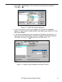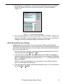
1
ISP Synario System
Design Tutorial
Technical Support Line: 1- 800-LATTICE or (408) 428-6414
ISPSYN-TT Rev 3.00
Copyright
This document may not, in whole or part, be copied, photocopied, reproduced,
translated, or reduced to any electronic medium or machine-readable form without
prior written consent from Lattice Semiconductor Corporation, (LSC).
The software described in this manual is copyrighted and all rights are reserved by
Lattice Semiconductor Corporation. Information in this document is subject to change
without notice.
The distribution and sale of this product is intended for the use of the original
purchaser only and for use only on the computer system specified. Lawful users of
this product are hereby licensed only to read the programs on the disks, cassettes, or
tapes from their medium into the memory of a computer solely for the purpose of
executing them. Unauthorized copying, duplicating, selling, or otherwise distributing
this product is a violation of the law.
Trademarks
The following trademarks are recognized by Lattice Semiconductor Corporation:
Generic Array Logic, ISP, ispATE, ispCODE, ispDOWNLOAD, ispGDS, ispStarter,
ispSTREAM, Latch-Lock, pDS+, RAL, RFT, and Twin GLB are trademarks of Lattice
Semiconductor Corporation.
E2CMOS, GAL, ispGAL, ispLSI, pDS, pLSI, Silicon Forest, and UltraMOS are
registered trademarks of Lattice Semiconductor Corporation.
Microsoft Windows and MS-DOS are registered trademarks of Microsoft Corporation.
IBM is a registered trademark of International Business Machines Corporation.
DATA I/O, and Synario are registered trademarks of Data I/O Corporation.
Lattice Semiconductor Corporation
5555 NE Moore Court
Hillsboro, OR 97124
(503) 681-0118
August 1996
ISP Synario System Design Tutorial
2
Limited Warranty
Lattice Semiconductor Corporation warrants the original purchaser that the Lattice
Semiconductor software shall be free from defects in material and workmanship for a
period of ninety days from the date of purchase. If a defect covered by this limited
warranty occurs during this 90-day warranty period, Lattice Semiconductor will repair
or replace the component part at its option free of charge.
This limited warranty does not apply if the defects have been caused by negligence,
accident, unreasonable or unintended use, modification, or any causes not related to
defective materials or workmanship.
To receive service during the 90-day warranty period, contact Lattice Semiconductor
Corporation at:
Phone: 1-800-LATTICE
Fax: 1 (408) 944-8450
E-mail: [email protected]
If the Lattice Semiconductor support personnel are unable to solve your problem over
the phone, we will provide you with instructions on returning your defective software
to us. The cost of returning the software to the Lattice Semiconductor Service Center
shall be paid by the purchaser.
Limitations on Warranty
Any applicable implied warranties, including warranties of merchantability and fitness
for a particular purpose, are hereby limited to ninety days from the date of purchase
and are subject to the conditions set forth herein. In no event shall Lattice
Semiconductor Corporation be liable for consequential or incidental damages
resulting from the breach of any expressed or implied warranties.
Purchaser’s sole remedy for any cause whatsoever, regardless of the form of action,
shall be limited to the price paid to Lattice Semiconductor Corporation for the Lattice
Semiconductor software.
The provisions of this limited warranty are valid in the United States only. Some states
do not allow limitations on how long an implied warranty lasts, or exclusion of
consequential or incidental damages, so the above limitation or exclusion may not
apply to you.
This warranty provides you with specific legal rights. You may have other rights which
vary from state to state.
ISP Synario System Design Tutorial
3
Table of Contents
Preface . . . . . . . . . . . . . . . . . . . . . . . . . . . . . . . . . . . . . . . . . . . . . . . . . . . . . . . . . . . . . . . . . . . . 5
What is in this Tutorial . . . . . . . . . . . . . . . . . . . . . . . . . . . . . . . . . . . . . . . . . . . . . . . . . . . . . . . .
Where to Look for Information . . . . . . . . . . . . . . . . . . . . . . . . . . . . . . . . . . . . . . . . . . . . . . .
Documentation Conventions . . . . . . . . . . . . . . . . . . . . . . . . . . . . . . . . . . . . . . . . . . . . . . . . . . .
Related Documentation . . . . . . . . . . . . . . . . . . . . . . . . . . . . . . . . . . . . . . . . . . . . . . . . . . . . . . .
Lattice Semiconductor . . . . . . . . . . . . . . . . . . . . . . . . . . . . . . . . . . . . . . . . . . . . . . . . . . . . .
Synario . . . . . . . . . . . . . . . . . . . . . . . . . . . . . . . . . . . . . . . . . . . . . . . . . . . . . . . . . . . . . . . . .
Software Support . . . . . . . . . . . . . . . . . . . . . . . . . . . . . . . . . . . . . . . . . . . . . . . . . . . . . . . . . . . .
Customer Hotline . . . . . . . . . . . . . . . . . . . . . . . . . . . . . . . . . . . . . . . . . . . . . . . . . . . . . . . . .
6
6
7
8
8
8
9
9
Chapter 1 Tutorial . . . . . . . . . . . . . . . . . . . . . . . . . . . . . . . . . . . . . . . . . . . . . . . . . . . . . . . . 10
Requirements. . . . . . . . . . . . . . . . . . . . . . . . . . . . . . . . . . . . . . . . . . . . . . . . . . . . . . . . . . . . . .
The Project Navigator . . . . . . . . . . . . . . . . . . . . . . . . . . . . . . . . . . . . . . . . . . . . . . . . . . . . . . .
Start ISP Synario . . . . . . . . . . . . . . . . . . . . . . . . . . . . . . . . . . . . . . . . . . . . . . . . . . . . . . . .
Add a Schematic to your Design . . . . . . . . . . . . . . . . . . . . . . . . . . . . . . . . . . . . . . . . . . . .
Complete the Design . . . . . . . . . . . . . . . . . . . . . . . . . . . . . . . . . . . . . . . . . . . . . . . . . . . . .
Add Design Attributes. . . . . . . . . . . . . . . . . . . . . . . . . . . . . . . . . . . . . . . . . . . . . . . . . . . . .
Create Simulation Test Vectors . . . . . . . . . . . . . . . . . . . . . . . . . . . . . . . . . . . . . . . . . . . . .
Compile Schematics and Test Vectors. . . . . . . . . . . . . . . . . . . . . . . . . . . . . . . . . . . . . . . .
Functional Simulation and Waveform Output . . . . . . . . . . . . . . . . . . . . . . . . . . . . . . . . . . .
Create a Symbol. . . . . . . . . . . . . . . . . . . . . . . . . . . . . . . . . . . . . . . . . . . . . . . . . . . . . . . . .
Fit the Design into a Lattice Semiconductor Part . . . . . . . . . . . . . . . . . . . . . . . . . . . . . . . .
Combine ABEL-HDL and Schematics . . . . . . . . . . . . . . . . . . . . . . . . . . . . . . . . . . . . . . . .
Create the ABEL-HDL Source File . . . . . . . . . . . . . . . . . . . . . . . . . . . . . . . . . . . . . . . . . . .
Compile ABEL-HDL . . . . . . . . . . . . . . . . . . . . . . . . . . . . . . . . . . . . . . . . . . . . . . . . . . . . . .
Simulate the Design . . . . . . . . . . . . . . . . . . . . . . . . . . . . . . . . . . . . . . . . . . . . . . . . . . . . . .
Fit the Design into a Lattice Part . . . . . . . . . . . . . . . . . . . . . . . . . . . . . . . . . . . . . . . . . . . .
ISP Synario System Design Tutorial
11
11
11
13
15
16
18
19
20
21
22
24
28
30
30
33
4
Preface
This preface contains sections about the following information:
■
■
■
■
What is in this Tutorial
Documentation Conventions
Related Documentation
Software Support
ISP Synario System Design Tutorial
5
What is in this Tutorial
What is in this Tutorial
This tutorial contains instruciton on the following:
■
■
■
■
■
■
■
■
Adding Schematics to Your Design
Adding Design Attributes
Creation of Simulation Test Vectors
Schematics and Test Vectors Compilation
Execution of Functional Simulation and Waveform Output
Symbol Creation
ABEL-HDL Creation and Compilation
Design Simulation
Where to Look for Information
Chapter 1, Installation – Lists what products you must have installed beore you can
use this tutorial. This chapter also contains operational notes and other information
that you might find useful before "Installation Requirements."
Chapter 2, Tutorial – Introduces the Synario Schematic tool and the provides
procedures to become adept at entering ABEL syntax, with a preview of the
Waveform viewer.
ISP Synario System Design Tutorial
6
Documentation Conventions
Documentation Conventions
The conventions in this tutorial are defined in the following table.
Convention
Italics
Definition and Usage
Italicized text represents variable input. For example:
design.1
This means you must replace design with the file name you used for all
the files relevant to your design.
Valuable information may be italicized for emphasis. Book titles also
appear in italics.
The beginning of a procedure appears in italics. For example:
To open a design:
Bold
Valuable information may be boldfaced for emphasis. Commands are
shown in boldface. For example:
edif2laf
Courier Font
Monospaced (Courier) font indicates file and directory names, and text
that the system displays. For example:
INPUT S2..S0,/SDI,Clock;
Bold Courier
Bold Courier font indicates text you type in response to system
prompts. For example:
dpm -if edif -of verilog
|...|
Vertical bars indicate options that are mutually exclusive; you can
select only one. For example:
-s [a|d]
“Quotes”
Titles of chapters or sections in chapters in this user manual are shown
in quotation marks. For example:
“Property File.”
✍ NOTE
Indicates a special note.
▲ CAUTION
Indicates a situation that could cause loss of data or other problems.
❖ TIP
Indicates a special hint that makes using the software easier.
⇒
Indicates a menu option leading to a submenu option. For example:
File ⇒ New
ISP Synario System Design Tutorial
7
Related Documentation
Related Documentation
In addition to this tutorial, the following documents are useful when using the ISP
Synario System.
Lattice Semiconductor
■
■
pDS+ Fitter User Manual
Lattice Semiconductor Data Book
Synario
■
■
■
■
■
ISP Synario System User Manual
Project Navigator User Manual
Equation & JEDEC Simulators User Manual
Schematic Entry User Manual
Waveform Tools Manual
ISP Synario System Design Tutorial
8
Software Support
Software Support
Customer Hotline
If you have any questions or problems with this software, please call Lattice
Semiconductor Applications Hotline at 1-800-LATTICE (1-800-528-8423) or
(408) 428-6414. The Hotline is available from 8:00 AM to 5:00 PM, Pacific Time.
Or, send e-mail to [email protected].
Information Need
ispLSI/pLSI
Applications Support
GAL/ispGAL/ispGDS
Applications Support
Literature
Customer Resource
USA & Canada
Other Locations
Telephone Hotline
1-800-LATTICE
1-800-528-8423
(408) 428-6414
Fax
(408) 944-8450
Bulletin Board
System
(408) 428-6417
E-mail
[email protected]
FTP Site
http://www.latticesemi.com/ftp/index.html
World Wide Web
http://www.latticesemi.com
Telephone Hotline
1-888-ISPPLDS
1-888-477-7537
Fax
(503) 681-3037
Bulletin Board
System
(503) 693-0215
E-mail
[email protected]
FTP Site
http://www.latticesemi.com/ftp/index.html
World Wide Web
http://www.latticesemi.com
Telephone Hotline
1-800-327-8425
Fax
(503) 681-3037
E-mail
[email protected]
FTP Site
http://www.latticesemi.com/ftp/index.html
ISP Synario System Design Tutorial
(503) 681-0118
(503) 681-0118
9
Chapter 1
Tutorial
The ISP Synario Tutorial, using a simple design example, will guide you through the
following:
■
■
■
■
■
■
■
■
■
■
■
■
■
■
Requirements
Start ISP Synario
Add a Schematic to Your Design
Complete the Design
Add Design Attributes
Create Simulation Test Vectors
Compile Schematics and Test Vectors
Execute Functional Simulation and Waveform Output
Create a Symbol
Combine ABEL-HDL and Schematics
Create the ABEL-HDL Source File
Compile ABEL-HDL
Simulate the Design
Fit the Design into a Lattice Semiconductor Part
ISP Synario System Design Tutorial
10
Requirements
Before you can proceed with this tutorial, you must have the following products
installed.
■
■
■
Synario Design Entry
ISP Synario Fitter
Win32s
Refer to the ISP Synario System User Manual for installation instructions.
The Project Navigator
From ISP Synario’s Project Navigator, you can perform a number of design functions
including accessing the components for your design and keeping track of the
necessary processing steps. You can open schematic and text editors, navigate
through your design hierarchy and more. This tutorial will familiarize you with the
Project Navigator and allow you to become adept at entering ABEL-HDL syntax, with
a preview of the Waveform viewer.
Start ISP Synario
1. Start the ISP Synario System by double-clicking on the ISP Synario icon in the
ISP Synario program group. The Synario Project Navigator window appears
(Figure 1-1).
Figure 1-1. Synario Project Navigator Window
ISP Synario System Design Tutorial
11
2. Select File ⇒ New Project... The Create New Project dialog box appears
(Figure 1-2).
Figure 1-2. Create New Project Dialog Box
3. In the C (home) drive, click to open synplsi, then highlight the examples
directory. In the Project File Name text box, type tutor.syn (Figure 1-2). Click
OK or press Enter.
4. In the Project Navigator, there are two sources: Untitled and Virtual Device. To
name your project, double-click on Untitled. A Project Title dialog box appears.
Type Demo Project in the Title field, then click OK (Figure 1-3).
Figure 1-3. Synario Project Navigator and Project Title Box
ISP Synario System Design Tutorial
12
5. Double-click on Virtual Device. You will see the Choose Device pop-up window.
Select ISP Synario Device list in the Device Kit field. A device list appears
(Figure 1-4).
Figure 1-4. Choose Device Window
6. Scroll through the device list until you find ispLSI 2032-150 TQFP44. Highlight this
device and click OK. You will be asked to confirm your choice since it will result in
changes in the Project Navigator design environment. Click Yes.
Add a Schematic to your Design
Design projects are made up of one or more sources, which can be schematics,
ABEL-HDL files, test vector files, or documentation files. In the following steps you will
add a blank schematic sheet source to your project, add several schematic symbols,
and connect them with nets.
7. With the 2032 device selected, notice the processes associated with this source.
From the menu bar, select Source ⇒ New...
8. In the New Source dialog box, select Schematic and click OK or press Enter. A
dialog box appears asking you to enter the name for a new schematic. Select the
path: c:\synplsi\examples and enter the file name demo.sch in the text field. Click
OK or press Enter.
NOTE: In order to avoid problems, it is a good idea to use a different name for
your source file than the project name.
9. The schematic editor appears with a blank schematic (Figure 1-5). From the menu
bar, select Add ⇒ Symbol.
ISP Synario System Design Tutorial
13
Figure 1-5. Schematic Editor Window
10. In the Symbol Libraries dialog box, select C:\...\generic\gates.lib from the library
list, then highlight the G_2AND symbol (Figure 1-6).
Figure 1-6. Symbol Libraries Window
11. Move the pointer back over the Schematic Editor; notice the AND gate attached to
your pointer. Place the gate by clicking on the schematic. Place another AND gate
below the first.
12. Move the cursor back to the Symbol Libraries dialog box and select the G_2OR
symbol. Place that gate to the right of the two AND gates.
13. From the Schematic Editor menu bar, select Add ⇒ Wire. Click on the output pin
of the top AND gate to start the wire. Each successive click will bend the wire (a
double-click will end the wire if it is not connected). Connect the wire to an input of
the OR gate with a single click. Repeat for the lower AND gate.
ISP Synario System Design Tutorial
14
14. Repeat the above procedure to add a g_d register from the REGS.LIB library and
a G_OUTPUT from the IOPADS.LIB. Connect them so that the schematic follows
the example (Figure 1-7).
Figure 1-7. Building the Schematic
Complete the Design
In this section, you will complete the schematic by adding the net names and I/O
Markers. When adding net names, you will use a feature of Synario that allows you to
add the net name and the net simultaneously. I/O Markers are the special symbols
that indicate what signals enter and leave a schematic. Nets cannot be left ‘dangling’,
they must have an I/O Marker. The markers assume the name of the net they are
attached to and are different from the I/O Pad symbols.
15. On the Schematic Editor menu bar, select Add ⇒ Net Name. The status bar at
the bottom of the screen will prompt you to enter the net name to add. Type A and
press Enter. The Net Name will be attached to your cursor.
16. Move the cursor to the uppermost input and click and hold on the unconnected
end of the net (i.e. the red box at the left end of the net) and drag to the left. This
will place the net name and create an input net simultaneously. The net name
should now be attached to the end of the net.
17. Repeat this procedure to add the net names ‘B’, ‘C’, ‘D’, and ‘CK’ to the inputs and
‘OUT’ to the output.
18. From the Schematic Editor menu bar, select Add ⇒ I/O Marker. The I/O Markers
dialog box appears. Choose Input.
ISP Synario System Design Tutorial
15
19. Move the cursor to the end of an input net (between the end of the net and the net
name) and click. An input marker appears with the net name inside of it. Move to
the next input and click again. Repeat until all inputs have I/O Markers.
20. Choose Output from the I/O Markers dialog box and click on the end of the output
net. The completed schematic should appear as shown in Figure 1-8.
Figure 1-8. Completed Schematic
Add Design Attributes
Attributes can be added to either symbols or nets. For this example, you will add a
LOCK attribute to the output pad symbol and a SCP/ECP (Start/End Critical Path)
attribute pair to an input path. Note that in Synario, pin attributes are actually added to
the I/O Pad symbols, not to the I/O Markers. Also note that I/O Pad symbols are only
necessary if you want to add attributes to a pin. Otherwise, you only need an I/O
Marker. The following procedure can also be used to lock an input pin, however it is
not shown.
21. From the Schematic Editor menu bar, select Add ⇒ Symbol Attribute. The
Symbol Attribute Editor dialog box appears. On the schematic, click on the I/O
Pad attached to the OUT net. A list of related attributes appears in the dialog box.
22. Select the SynarioPin=4 attribute and replace the * in the text box with the
number 4 as shown in Figure 1-9. Close the dialog box. Notice that the number 4
has been added in the I/O Pad symbol in the schematic.
ISP Synario System Design Tutorial
16
Figure 1-9. Symbol Attribute Editor
23. The steps are similar for adding a Net or Path attribute. From the Schematic Editor
menu bar, select Add ⇒ Net Attribute. The Net Attribute Editor dialog box
appears. On the schematic, click on the net that connects input C to the AND
gate. The list of related attributes appears in the dialog box.
24. Select the CriticalPath= attribute and type S,path1 in the text box as shown in
Figure 1-10. The S signifies that Start of the path and path1 comprise the unique
name for the path attribute. You will not see anything on your schematic for this
attribute.
Figure 1-10. Net Attribute Editor
25. On the schematic, click on the net that connects the OR gate with the D flip-flop.
In the Net Attribute Editor dialog box, enter E,path1. This will signify the end of
the critical path named ‘path1’. Close the dialog box.
26. From the Schematic Editor menu bar, select File ⇒ Save to save your design.
Select File ⇒ Exit to close the Schematic Editor window.
ISP Synario System Design Tutorial
17
Create Simulation Test Vectors
In ISP Synario, you can use one or more sets of test vectors to simulate the function
of a device. For the purposes of this tutorial, you will enter a simple test vector.
27. In the Synario Project Navigator, highlight the ispLSI 2032-150 TQFP44 device.
From the menu bar, select Source ⇒ New. A New Source dialog box appears.
Highlight Abel Test Vectors and click OK or press Enter.
28. The New File dialog box and a blank Synario Text Editor window appears. Enter
the file name demo as shown in Figure 1-11 for your test vector file name. Click
OK or press Enter.
Figure 1-11. Synario Text Editor with the New File Dialog Box
29. In the Synario Text Editor window, type the following, keeping aware of case
sensitivity (‘c’ versus ‘C’):
module demo;
c,x = .c.,.x.;
CK,A,B,C,D,OUT PIN;
TEST_VECTORS
([CK,A,B,C,D]->[OUT])
[c , 0 , 0 , 0 , 0]->[x];
[c , 0 , 0 , 1 , 0]->[x];
[c , 1 , 1 , 0 , 0]->[x];
[c , 0 , 1 , 0 , 1]->[x];
END
30. When finished, select File ⇒ Save from the Synario Text Editor menu bar to save
your test vector file. Select File ⇒ Exit. Synario returns you to the Project
Navigator, which appears as in Figure 1-12.
ISP Synario System Design Tutorial
18
Figure 1-12. Synario Project Navigator
Compile Schematics and Test Vectors
Now that you have created sources for your project, the next step is to execute the
processes associated with each source. By selecting each source, you can see the
different processes that can be executed. You will compile the schematic and the test
vectors separately.
31. In the Synario Project Navigator window, highlight the schematic source demo
(demo.sch) in the Sources in Project list. Double-click on Compile Schematic in
the Processes list. A status dialog box (Figure 1-13) appears briefly. When the
process is finished, the Compile Schematic process will have a green check mark
next to it indicating a successful compile.
Figure 1-13. Synario Process Status Dialog Box
32. In the Synario Project Navigator window, highlight the test vector source
demo.abv. Double-click on Compile Test Vectors in the Processes list. When
finished, Compile Test Vectors shows a green check mark next to it.
ISP Synario System Design Tutorial
19
Functional Simulation and Waveform Output
The ISP Synario System includes a functional simulator and waveform viewer. The
following steps will demonstrate how you can execute the process and have the
Navigator complete all the necessary steps to achieve the results. In this case, you
want to see the waveform output of your vector simulation. The Navigator will
simulate the vectors and open the waveform environment for you.
33. With the test vector source (demo.abv) highlighted, double-click on Equation
Simulation Waveform in the Processes list. Synario simulates the equations and
the Waveform Viewer window appears (Figure 1-14).
Figure 1-14. The Waveform Viewer
34. To see the waveforms, select Edit ⇒ Show from the Waveform Viewer menu bar.
A Show Waveforms Dialog Box (Figure 1-15) appears.
Figure 1-15. The Show Waveforms Dialog Box
35. One at a time, highlight each signal name that you want to see and press Show.
The waves you selected will appear in the Waveform Viewer window in the order
you chose them (Figure 1-16). Select File ⇒ Exit to close the Waveform Viewer.
A dialog box will appear, asking you to confirm changes to PLA.wav.
ISP Synario System Design Tutorial
20
Figure 1-16. A Completed Waveform
Create a Symbol
A useful feature of the Synario tool is the ability to quickly create a symbol for a
schematic. By doing this you create a reusable macro that can be placed on a higher
level schematic sheet.
a. Open the schematic file by double-clicking on the schematic source,
demo.sch.
b. In the schematic editor menu bar, select File ⇒ Matching Symbol.
c. Select File ⇒ Exit to close the schematic.
d. The symbol has been created and added to your symbol list. You will use this
symbol in the next section.
ISP Synario System Design Tutorial
21
Fit the Design into a Lattice Semiconductor Part
You have now completed the design and simulation of your example design. If you
plan to proceed to the next section, Combine ABEL-HDL and Schematics, you need
not complete the steps remaining in this section. Otherwise, the last process is to fit
the design into a Lattice Semiconductor pLSI part. Since you selected a part earlier in
this example, the remaining steps are straightforward.
36. Select the ispLSI 2032-150 TQFP44 source and observe the related processes.
Double click on the process Fit Design. A Synario Process dialog box appears
momentarily (Figure 1-17). The Navigator finishes compiling the source, then links
the source files together. Finally, the Navigator partitions and fits the design into
the LSC part.
Figure 1-17. Synario Process Dialog Box
37. When the process is complete, the Synario Project Navigator window returns
(Figure 1-18). Note that check marks have been added to Fit Design processes
that have been successfully completed.
Figure 1-18. Synario Project Navigator After the Fitter Process
ISP Synario System Design Tutorial
22
38. Double click on ISP Synario Fitter Report in the Processes list to see the statistics
related to the fitting of your design (Figure 1-19).
Figure 1-19. Design Statistics After Design Fitting
ISP Synario System Design Tutorial
23
Combine ABEL-HDL and Schematics
In this section, you will create a small ABEL-HDL design, then connect it to the
schematic from the previous steps on a top-level schematic. This complete design will
be simulated and compiled into an ispLSI device.
39. If you quit from ISP Synario after the last section, re-start by double-clicking on the
icon in the ISP Synario System Program Group. Your Navigator screen should
look like the one in Figure 1-20. If not, make sure all the previous steps were
completed correctly.
Figure 1-20. Synario Project Navigator
40. With the 2032 device selected, select Source ⇒ New from the Synario Project
Navigator menu bar. In the dialog box, select Schematic and click OK. Select the
path: c:\synplsi\examples and enter the file name top.sch in the text box. Click
OK. You are now in the Schematic Editor.
41. Add the symbol for the schematic you created in Section 1. Select Add ⇒
Symbol. The Symbol Libraries dialog box appears with the Local library selected.
Notice the demo symbol in the lower text box (Figure 1-21). Select the demo
symbol and place it on your schematic.
ISP Synario System Design Tutorial
24
Figure 1-21. Schematic Editor with Symbol Libraries Dialog box
The next step is to create a top level symbol for your ABEL-HDL design file. A symbol
can be created for any lower level design module as long as you know its interface.
The actual ABEL-HDL file for your design will be completed in a later step.
42. In the schematic editor, select Add ⇒ New Block Symbol... In the dialog box that
appears, type abeltop in the Block Name text box, IN1,IN2,IN3 in the Input
Pins text box, and OUT1,OUT2,OUT3,OUT4 in the Output Pins text box
(Figure 1-22). Click Run.
Figure 1-22. New Block Symbol Dialog Box
ISP Synario System Design Tutorial
25
43. A symbol will be added to your local library and the symbol will be attached to your
cursor. Place the symbol to the left of the demo symbol. Click with the right mouse
button to display the Symbol Libraries dialog box (Figure 1-23). Note the abeltop
symbol in the Local library. Close the dialog box.
Figure 1-23. Adding Symbols from the Local Library
44. Complete the top level schematic by adding the necessary wires, net names, and
I/O Markers to finish the design (Figure 1-24). Refer to the instructions for adding
nets and symbols (page 1-15) if you need assistance. When you are finished,
save your design and exit the schematic editor.
ISP Synario System Design Tutorial
26
Figure 1-24. Completed Abeltop Design
If you are interested in verifying the correctness and consistency of your top level
design, you can move through the design levels using the Hierarchy Navigator
feature. A number of editing functions are available through the Navigator.
45. In the Sources in Project list of the Synario Project Navigator window, highlight the
top level schematic (top.sch). In the Processes list, double-click on Navigate
Hierarchy. A Building Hierarchy message box will appear briefly, then the
Hierarchy Navigator window appears with your top level design.
46. Select View ⇒ Push/Pop. The cursor becomes a cross-hairs. Click on the
desired symbol. The Hierarchy Navigator will open the sheet for that symbol at the
next level. If you click on a symbol that is a primitive cell, a message at the bottom
of the Navigator window will prompt you.
47. Select File ⇒ Exit to close the Hierarchy Navigator. You will be asked to save
changes you made, if any.
ISP Synario System Design Tutorial
27
Create the ABEL-HDL Source File
Now you need to create the ABEL-HDL source file and link it to the symbol on the top
level schematic. The Project Navigator makes this simple.
48. Your Navigator should look like the one in Figure 1-25. The “?” icon for abeltop
means that the source is unknown since you have not created it yet. Also notice
the hierarchy indents the abeltop and demo sources under the top schematic.
Figure 1-25. Synario Project Navigator
49. To create the source, highlight the abeltop source, then select Source ⇒ New. In
the New Source dialog box, choose ABEL-HDL Module and click OK. A Synario
Text Editor appears with the New ABEL-HDL Source dialog box (Figure 1-26).
Figure 1-26. New ABEL-HDL Source Dialog Box
ISP Synario System Design Tutorial
28
In order for the file to be linked to the symbol, the Module Name must match the
symbol name. The File Name does not need to match the symbol name, but to make
things simple in this tutorial, you will make them the same. Fill in the text fields as
follows:
Module Name: abletop
File Name: abeltop.abl
Title: This is the Top Level ABEL file
Click OK. You will now be in the Synario Text Editor and will see the ABEL-HDL
framework already started for you.
50. Enter the code as follows. Make sure that you enter it between the TITLE
statement and the END statement as shown in Figure 1-27.
"Inputs
IN1,IN2,IN3 pin;
"Outputs
OUT1,OUT2,OUT3,OUT4
pin;
Equations
OUT1=IN1 & !IN3;
OUT2=IN1 & !IN2;
OUT3=!IN1 & IN2 & IN3;
OUT4=IN2 & IN3;
Figure 1-27. Synario Text Editor with Code Entered
51. Select File ⇒ Save, then File ⇒ Exit. Notice in the Project Navigator that the icon
next to the abeltop source has changed. This means you have an ABEL-HDL file
associated with this source and it is linked correctly.
ISP Synario System Design Tutorial
29
Compile ABEL-HDL
52. In the Sources in Project field of the Project Navigator, select the abeltop source
(abeltop.abl). In Processes for Current Source, double-click on Reduce Logic.
The Navigator will take care of running the Compile Logic process before it
executes the Reduce Logic process. When the process is finished, your Navigator
should match the one in Figure 1-28.
Figure 1-28. Synario Project Navigator after ABEL-HDL Compile
Simulate the Design
You will now simulate the entire design. To do this you need a test vector (.ABV) file.
For the purpose of this tutorial, you will just modify the one you created earlier.
53. Double-click on the demo.abv source. The Synario Text Editor appears with the
syntax you input in step 29. Modify the text as follows:
module demo;
c,x = .c.,.x.;
CLK,TOPIN1,TOPIN2,TOPIN3,TOPOUT PIN;
TEST_VECTORS
([CLK,TOPIN1,TOPIN2,TOPIN3]->[TOPOUT])
[c , 0 , 0 , 0]->[x];
[c , 0 , 0 , 1]->[x];
[c , 0 , 1 , 0]->[x];
[c , 0 , 1 , 1]->[x];
[c , 1 , 0 , 0]->[x];
[c , 1 , 0 , 1]->[x];
[c , 1 , 1 , 0]->[x];
[c , 1 , 1 , 1]->[x];
END
ISP Synario System Design Tutorial
30
Figure 1-29. Synario Text Editor with Text Vector Syntax
54. When you are finished, select File ⇒ Save, then File ⇒ Exit.
55. In the Navigator, with Compile Test Vectors still selected, double-click on the
Equation Simulation Waveform process. Since you edited the existing test vector
file instead of creating a new one, you will get an error message (Figure 1-30)
saying that the signal names you used earlier cannot be found. Accept the
message and close the Report Viewer.
ISP Synario System Design Tutorial
31
Figure 1-30. Synario Report Viewer and Error Message Window
56. The Waveform Viewer window appears. To see the waveforms, select
Edit ⇒ Show. The Show Waveforms dialog box appears with all your signal
names, as well as the intermediate ones, listed for you.
57.One at a time, select TOPIN1, TOPIN2, TOPIN3, TOPOUT, and CLK and click
Show. Each of these signals will be visible in the Waveform Viewer
(Figure 1-31). Close the Show Waveforms dialog box. Select File ⇒ Save in the
Waveform Viewer window, then File ⇒ Exit.
Figure 1-31. Show Waveforms dialog box and Waveform Viewer
ISP Synario System Design Tutorial
32
Fit the Design into a Lattice Part
You have completed the design and the simulation of your mixed schematic and
ABEL-HDL design. The only step remaining is to fit the design into a Lattice
Semiconductor ispLSI part. Since you selected a part in the beginning steps, the
remaining steps are straightforward.
58. From the Sources in Project portion of the Synario Project Navigator, select the
ispLSI 2032-150 TQFP44 source and observe the related processes that have
been created.
59. In the Processes for Current Source list, double-click on Fit Design. This will force
the Navigator to finish compiling the source and to link the source files together
before trying to partition and fit the design into a LSC part. The Synario Project
Navigator will add check marks to successfully completed processes (Figure
1-32).
Figure 1-32. Synario Project Navigator After Successful Design Fit
60. Note that the pDS+ Fitter has several user controls that can be accessed from the
Navigator; highlight Fit Design and click Properties at the bottom of the Navigator
window. You will see a dialog box with a list of pDS+ Fitter properties in it. See the
pDS+ Fitter User Manual for an explanation of these properties.
ISP Synario System Design Tutorial
33
61. To see all of the statistics related to the fitting of your design, double click on ISP
Synario Fitter Report. The tutor.rpt window appears within the Synario Report
Viewer (Figure 1-33). You can scroll through the report window for your design
data.
Figure 1-33. Synario Report Viewer and tutor.rpt windows
CONGRATULATIONS! You have completed the design example and are now familiar
with the major functions of the ISP Synario System.
ISP Synario System Design Tutorial
34