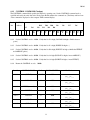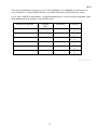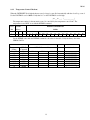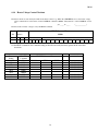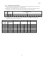
1
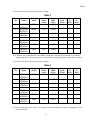
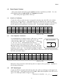
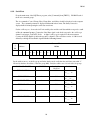
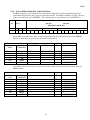
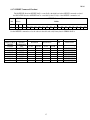
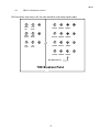
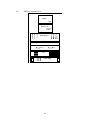
P0396
Relativity Mission / Gravity Probe B
Telescope Readout Electronics
P0396
Quality Assurance Test Procedure
For
Telescope Readout Electronics (TRE)
Ground Support Equipment Rack (GSE)
January 24, 2010
Prepared and Approved by:
Robert Fujimoto (REE)
Approval:
Paul Ehrensberger (TRE Manager)
Approval:
Bob Farley (REE)
Approval:
Ben Taller (QA)
Approval:
John Turneaure (Hardware Manager)
1
P0396
Contents
1.0
2.0
3.0
4.0
5.0
6.0
7.0
8.0
9.0
1.0
General Description ............................................................................... 2
Reference Documents ............................................................................ 2
Test Facilities ......................................................................................... 2
General Requirements ............................................................................ 2
Safety / Security Requirements .............................................................. 3
Hardware Under Test ............................................................................. 3
Power Level Checkout ........................................................................... 4
Data Acquisition Checkout..................................................................... 5
Digital Signal Checkout.......................................................................... 8
General Description
This document is the Quality Assurance Test Procedure for the Telescope Readout Electronics GROUND
SUPPORT EQUIPMENT (GSE). The purpose of the QA test is to provide traceability to test results
performed on the FWD TRE electronics and the Detector Package Assembly (DPA).
2.0
Reference Documentation
Functional Test Procedure For Fwd Flight Unit Subassemblies dated 09 February 1998.
LMMS Handbook on ESD - LMMS F03581
3.0
Test Location
Telescope Electronics Development Lab, Cedar Hall, Stanford University, Stanford, CA
4.0
General Requirements
4.1 Test will be performed under the environmental conditions existing in Cedar Hall.
4.2 Any red lines to the procedure shall require the approval and initial of the Stanford QA and RE.
4.3 In order to expedite test operations, unless specifically noted, the sequence in which major sections or
subsections are performed may be altered at the discretion of the REE or his representative. Rationale must
be documented and initialed by REE.
4.4 PA or their representative shall be present to witness and verify the test is performed as described in the test
procedure, and stamp each page of the procedure as it progresses. Notify Quality Assurance Engineering at
least 48 hrs., prior to the start of testing. In the event of a failure during the execution of testing Quality
Assurance shall be contacted. Any red lines made to this procedure shall be initialed by a program QA
Engineer prior to his/her final sign off..
4.5 Initial and date (
accomplished.
) the appropriate space in the test data sheet to verify each task has been
2
P0396
4.6 Serial numbers of test equipment used during this test shall be recorded in the “List of Equipment” log
sheet.
4.7 Test operators shall read this procedure in its entirety and resolve any apparent ambiguities prior to
beginning this test.
5.0
Safety / Security Requirements
5.1 Standard safety practices to insure safety to personal an and prevent damage to equipment shall be
observed during performance of this test.
5.2 Ensure that power is removed from cable assemblies before connecting and disconnecting cable connectors.
5.3 Examine all mating connectors before attempting to mate them and remove any foreign particles. Look
for any damaged pins or sockets. Ensure that key ways are aligned. Do not force the coupling action if
excessive resistance is encountered.
5.4 Protect all electrical connectors with Connector Savers or plastic caps when the connectors are not mated.
5.5 Care in handling electronic equipment shall be taken in accordance with the LMMS Handbook on
Electrostatic Discharge LMSC F03581 to prevent damage caused by electrostatic discharge.
6.0
Hardware Under Test
The hardware under test will consist of the Telescope Readout Electronics (TRE) Ground Support
Equipment(GSE) Test Rack.
6.1
The following items comprise the GSE Support Rack.
Name/Description
Rack Mount Oscilloscope
Rack Mount Computer with
Custom SRE Emulator Board
& A/D Converter Board
Rack Mount Monitor &
Keyboard
Custom Test Cables
Rack Mount Power Supply
Software
6.2
Manufacturer/Model No. Part No.
Tektronix TAS220 or TDS220
Rack Mount PC 500
Stanford / LMMS 8A01271
Computer Boards CIO-DAS1402
Qty.
1
1
1
Stanford / LMMS - 8A01272
Stanford / LMMS
SQUID.exe V3.51 or Higher
1
1
1
The following support equipment is required for QA Calibration of the GSE.
Name/Description
Manufacturer/Model No. Part No.
3
Qty.
P0396
TRE Engineering Unit
TRE Detector Simulator
TRE Rev. C Detector in LN2
Dewar
Rackqual Testaid
Voltage Calibrator
Precision Multimeter
Voltmeter
Digital Oscilloscope
Precision Function Generator
6.3
Stanford / LMMS
Stanford / LMMS
Stanford / LMMS
1
1
1
Stanford / LMMS
Datel - DVC 8500 or equivalent
HP - 3458A or equivalent
Fluke 87 or equivalent
Tektronics TDS 420A or equivalent
Wavetek Model 144 or equivalent
1
1
1
1
1
1
Calibration
Check to ensure the test equipment is calibrated prior to start of test. Record the calibration due dates
in the “List of Equipment” para. 13.0.
7.0
Power Level Checkout
For the GSE Rack checkout disconnect the Engineering Unit from the GSE(connector 15 and connector 17
open) and disconnect any Detector connected to the GSE. Turn the power supply on.(AC power switch,
+5v switch and +15v switch)
7.1.1 Connect the voltmeter (- terminal) to pin 12 of connector 15 , and the(+ terminal) to pin 11. Record the
value in table 1 below.
7.1.2 Connect the voltmeter(- terminal) to pin 31 of connector 15, and the (+ terminal) to pin 30. Record its
value in the table. Verify that the voltages are within the specified limits.
7.1.3 Connect the voltmeter (- terminal) to pin 12 of connector 17, and the (+ terminal) to pin 11. Record the
value in table 1 below.
7.1.4 Connect the voltmeter (-terminal) to pin 12 of connector 17, and the (+ terminal) to pin 13. Record its
value in the table.
7.1.5 Connect the voltmeter (-terminal) to pin 31 of connector 17 , and the (+ terminal) to pin 30. Record its
value in the table.
7.1.6 Connect the voltmeter (-terminal) to pin 31 of connector 17, and the (+ terminal) to pin 32. Record its
value.
Verify that all voltages are within the specified limits. Turn off the power supply.
4
P0396
Table 1
Para.
No.
Probe Point
Signal
Name
7.1.1
Connector 15
Pin 12-11
Connector 15
Pin 31-30
Connector 17
Pin 12-11
Connector 17
Pin 12-13
Connector 17
Pin 31-30
Connector 17
Pin 31-32
7.1.2
7.1.3
7.1.4
7.1.5
7.1.6
8.0
+5 V supply
Lower
Limit
(Volts)
+4.94V
Upper
Limit
(Volts)
+5.06V
+5 V supply
+4.94V
+5.06V
+15 V
supply
-15 V
supply
+15 V
supply
-15 V
supply
+14.8V
+15.2V
-15.2V
-14.8V
+14.85V
+15.2V
-15.2V
-14.8V
Actual
Value
(Volts)
Pass
or
Fail
Initials
&
Date
Data Acquisition Checkout
8.1 With no Engineering Unit or Detector connected to the GSE (Connector 15 and Connector 17 open), turn
on the power supply. From the SQUID directory on the computer, run squid.exe. From the command menu
note the display “GP-B SQUID and TELESCOPE Testing Vx.x. Record the SQUID program version
number.
Version No. ______ (__________)
Go to the Global Enable menu and enable all “A” side commands and telemetry. Return to the main
menu(ESC). Enter the command menu. Select TRE X.
8.2 (Connect XPSIGLO to XPSIGHI (shorted) with a BNC cable. Monitor the voltages on the telemetry
display. Read and record the voltage reading for XPSIG.
Table 2
Input
Signal
Output
Signal
XPSIGHI/
XPSIGLO
XPSIG
Lower
Limit
(Volts)
-0.01V
Upper
Limit
(Volts)
+0.01V
Actual
Value
(Volts)
Pass
or
Fail
Initials
&
Date
8.3.1With no Engineering Unit connected to the GSE. Connect the voltage calibrator to the voltage inputs on
the breakout panel labeled XPSIGHI and XPSIGLO. Set the voltage calibrator to 9.990
volts. Verify the setting using a calibrated voltmeter. Monitor the corresponding reading on the telemetry
page and record the value.
Repeat the voltage input and measure for each input designated in table 3. Monitor and record the
corresponding values from the telemetry display.
5
P0396
8.3.2 Reverse the input polarity and repeat the readings.
Table 3
Para.
No.
Input
Signal
Output
Signal
8.3.1
XPSIGHI/
XPSIGLO
XNSIGHI/
XNSIGLO
XHNSHI/
XHNSLO
8.3.1
8.3.1
8.3.2
8.3.2
8.3.2
XPSIGHI/
XPSIGLO
XNSIGHI/
XNSIGLO
XHNSHI/
XHNSLO
XPSIG
Lower
Limit
(Volts)
+9.99V
Upper
Limit
(Volts)
+10.00V
XNSIG
+9.99V
+10.00V
XHNS
+9.9V
+10.00V
XPSIG
-9.99V
-10.00V
XNSIG
-9.99V
-10.00V
XHNS
-9.99V
-10.00V
Actual
Value
(Volts)
Pass
or
Fail
Initials
&
Date
8.4.1 Return to the command menu. Select TRE Y. Repeat the voltage input and measure for each input
designated in table 3. Monitor and record voltages on the corresponding values on the telemetry display.
8.4.2 Reverse the input polarity and repeat the readings.
Table 4
Para.
No.
Input
Signal
Output
Signal
8.4.1
YPSIGHI/
YPSIGLO
YNSIGHI/
YNSIGLO
YHNSHI/
YHNSLO
YPSIGHI/
YPSIGLO
YNSIGHI/
YNSIGLO
YHNSHI/
YHNSLO
8.4.1
8.4.1
8.4.2
8.4.2
8.4.2
YPSIG
Lower
Limit
(Volts)
+9.99V
Upper
Limit
(Volts)
+10.00V
YPSIG
+9.99V
+10.00V
YHNS
+9.99V
+10.00V
YPSIG
-9.99V
-10.00V
YPSIG
-9.99V
-10.00V
YHNS
-9.99V
-10.00V
Actual
Value
(Volts)
Pass
or
Fail
Initials
&
Date
8.5 If any readings from para. 8.0 are out of range, perform the calibration procedure in Appendix A , then
repeat section 8.0.
6
P0396
8.6 Turn off the power supply. Disconnect the cables to the breakout panel.
7
P0396
9.0
Digital Signals Checkout
Turn on the computer and run the program squid.exe from the c:\squid directory in DOS.
[Global Enable] menu and enable all side “A” commands and telemetry.
Turn on the power supply and the oscilloscope.
9.1
Go to the
Clock Level Verification
Connect the oscilloscope in the test rack to be triggered by the rising edge of the ATC strobe, with the
time-base set to 1ms per division. Using a Microtip test probe connected to the oscilloscope input
through a banana to BNC adapter, verify that the voltage levels of the clock waveforms on the following
pins of connector 15 are between zero volts and +4 volts. (Low 0.2 ±0.4V and High +3.9 ±0.4V).
Pin
OK
Pin
OK
1
2
4
5
7
8
15
16
17
18
21
22
24
25
27
28
33
34
35
36
_____)
All pins are OK _____ (
9.2
Source Impedance Verification
Use the RACKQUAL test aid that contains a 1.5K resistor to verify the
Test Aid to Verify Source Impedance of
Digital Lines from TRE Test Rack.
source impedance of the clock lines. Connect the test aid to the
oscilloscope using a BNC cable. Connect the black
banana jack
on the test box to the black banana jack on the test
rack
5 volt power supply (lowest panel on the test rack). Connect the
Microtip test probe to the red banana jack on the test aid. Probe the
same pins of connector 15, and verify that the clock levels now swing
between zero and 1.8 volts. (Low 0.16 ±0.2V and High 1.74 ±0.2V).
(Each clock line should have a series resistor of the same size as the test box, hence the voltage measured is
half of the open circuit voltage.)
Red
Banana Jack
BNC
1.50K
Black
Banana Jack
Pin
OK
Pin
OK
1
2
4
5
7
8
15
16
17
18
21
22
24
25
27
28
33
34
35
36
All pins are OK _____ (
Monitor the voltage waveforms on the breakout panel, use a digital oscilloscope window
the following measurements:
9.4
_____)
capability for
ATC Strobe Signal
Connect the ATC Strobe signal on the breakout panel to the oscilloscope and trigger on that signal or the
DAC Strobe signal. Verify that the pulse period is 100ms.(10hz) and the amplitude of the ATC strobe is
approx. 5V. and the pulse width to be approx. 58 µS
Waveform is as described: yes___no___. (
_____)
8
P0396
9.5
DAC Strobe
Connect the DAC Strobe signal on the breakout panel to the oscilloscope and trigger on the ATC Strobe.
Verify that the frequency of the waveform is approx. 2.2 kHz.
Waveform is as described:
9.6
yes___no___. (
____)
68 kHz clk
The rising edge to rising edge of the 68.2 kHz clock determines the bit data in the SERIAL DATA
stream. The data is clocked in on the falling edge.
Connect the 68 kHz clk signal on the breakout panel to the oscilloscope and trigger on the ATC Strobe.
Verify that the frequency of the waveform is approx. 68.2 kHz.
Waveform is as described: yes___no___ (_______)
9.7
X Command Data Enable
Go to the command group menu select the TRE X command group. The X Data Enable signal gates the
serial data in the six TRE X commands. There are six corresponding pulses on the X DATA ENABLE
signal.
Connect the X Data Enable signal on the breakout panel to the oscilloscope and trigger on the ATC
Strobe. The X Data Enable goes true on a rising of the 68.2kHz clock and remains true for 20
cycles.Then it goes false on the rising edge of the next clock cycle.
Verify that there are six pulses each with a pulse width of approx. 293µS.
Waveform is as described: yes ___ no ___. (
9.8
_____)
Y Command Data Enable
Go to the command group menu select the TRE Y command group. The Y Data Enable signal gates the
serial data in the six TRE Y commands. There are six corresponding pulses on the Y DATA ENABLE
signal.
Connect the Y Data Enable signal on the breakout panel to the oscilloscope and trigger on the ATC
Strobe. Verify that there are six pulses each with a pulse width of approx. 293µS.
Waveform is as described:
9
yes ___
no ___. (
)
P0396
9.9.0 Serial Data
From the main menu of the SQUID test program, select [Commands] then [TRE X].
the X-axis command groups.
ENABLE each of
The six commands: Control, Etemp, Heat, Clamp, Bias, and Offsets should be displayed on the computer
screen. The command parameter is displayed underneath in hex format. The binary format also
displayedwill aid in interpreting the serial data waveforms.
Set the oscilloscope to observe the six X-axis enable pulses and the serial data which corresponds to each
of the six command groups. Connect the Serial Data signal on the break out panel to the oscilloscope
channel 1 and trigger on the ATC Strobe. A digital oscilloscope is required for this measurement.
Connect the X Data Enable of the breakout panel to channel 2. The serial data consists of a 20-bit word
defined bye the high X Data Enable signal with the following format.
Leadin
g
Command
Command Data
Address
16 bits
Bit
1
A2
A1
A0
D
D
D
D
D
D
15
14
13
12
11
10
HEX 3
D9
D8
D7
HEX 2
D6
D5
D4
D3
HEX 1
D2
D1
HEX 0
Set the window cursors on the first group and in the window mode verify that the serial data starts with “1”
followed by the three bit address of the first group (001). Verify the address word of each of the six groups.
COMMAND GROUPS
ADDRESS
TRE X CONTROL
1
Leading Bits
Observed
1001
Verification
yes ___ no
___
TRE X DTEMP
2
1010
TRE X HEATER
3
1011
yes ___ no ___
yes ___ no___
TRE X CLAMP
4
1100
yes ___ no
___
TRE X BIAS
5
1101
yes ___ no
___
TRE X OFFSETS
6
1110
yes ___ no
___
(
10
)
D0
P0396
9.9.1 CONTROL COMMAND Checkout
The CONTROL command field specifies the TRE axis operating state. Set the CONTROL command word as
specified and verify the serial data at the X axis Data Enable matches the command set. (The binary and hex form
of the command is displayed on the computer TRE command display.
Lead
CONTROL
Bit
Address
CONTROL Command Data
D5
0
1
9.9.1
0
1
X
D4
X
X
CO
LD
ON
D12
D11 D10
D9
D3
D2
D1
D0
INH
SIG
INH
CY
C
INV
GA
T
INV
RST
CTR
LHE
T
LO
WG
AIN
D8
CHA
NLC
K
D7
AM
UX
A4
AM
UX
A3
D6
AM
UX
A2
AM
UX
A1
AM
UX
A0
Set the CONTROL word to 0000h . Verify that all bits in the COMMAND data are low.
9.9.2 Set the CONTROL word to 1000h . Verify that bit 12 is high (COLDON bit high to Enable detector
power)
9.9.3
Set the CONTROL word to 0800h . Verify that bit 11 is high (INHSIG bit high to )
9.9.3 Set the CONTROL word to 0400h . Verify that bit 10 is high (INHCYC bit high to inhibit the FETRST
and AMPGAT pulses)
9.9.4
Set the CONTROL word to 0200h . Verify that bit 9 is high (INVGAT bit high to invert AMPGAT ).
9.9.5
Set the CONTROL word to 0100h . Verify that bit 8 is high (INVRST bit high to invert FETRST)
9.9.6
Return the CONTROL word to 0000h.
Para. No.
CONTROL WORD
Bit Set
9.9.1.1
(CLEAR)
NONE
COMMAND HEX
Verification
0000
yes___no___
9.9.1.2
COLDON
12
1000
yes___no___
9.9.1.3
INHSIG(not used)
11
0800
9.9.1.4
INHCYC
10
0400
9.9.1.5
INVGAT
9
0200
yes___no___
yes___no___
yes___no___
9.9.1.6
INVRST
8
0100
yes___no___
9.9.1.7
(CLEAR)
NONE
0000
yes___no___
(
11
)
P0396
Verify the Analog Multiplexer Sequencer control. Set the CONTROL word to 0020h(Monitored Channel Lock
true). Verify that bit 5 is high (CHANLCK high to load AMUX channel data and hold multiplexer counter).
9.9.1.8 Set the CONTROL word to 0021h to select monitored channel 1. Verify bit 0 and bit 8 (MUXA0) is high
Verify Monitored Channel selections using CONTROL word.
SELECTED CHANNEL
MUXA[0-4]
1
CONTROL
HEX
0021
9
0029
09
6
0026
06
Verification
01
yes___no___
yes___no___
yes___no___
22
0036
16
yes___no___
16
0030
10
0
0020
00
yes___no___
yes___no___
(_____________)
12
P0396
9.9.2
Temperature Control Checkout
When the CNTRLHET bit is high the heater control voltage is controlled automatically with the closed loop control.
Set the CONTROL word = 0080h. Verify that bit 7 on the CONTROL word is high.
yes __ no ___. (_____________)
The temperature setting for the automatic control is controlled by the temperature control DAC. The
temperature control DAC is set with the DTEMP command.
Lead
DTEMP
DTEMP Command Data
Bit
Address
16 bits
TEMPC0[0-11]
1
0
1
0
X
X
X
X
D11
D10
D9
D8
D7
D6
D5
D4
D3
D2
D1
Set the DTEMP value with the DTEMP command to the values in the table. Verify the binary data in the
SERIAL DATA.
Temperature
Setting
Decimal
240
273
1686
2056
3855
4095
0
DTEMP
Command
Hex
00F0h
0111h
0696h
0808h
0F0Fh
0FFFh
0850h
DTEMP Command Data
b11-b8
b7-b4
b3-b0
13
initial & date
(____________)
(____________)
(____________)
(____________)
(____________)
(____________)
(____________)
(____________)
D0
P0396
9.9.4 Heater Voltage Control Checkout
The heater current is controlled by the DAC in the heater control loop. When the CTRLHET bit is low, the heater voltage
can be commanded to a fixed value. Set the CONTROL command = 0000h. Verify that bit 7 of the CONTROL word is
low.
yes ____ no ____
(____________)
The fixed value of heater voltage is set by the HEAT command.
Lead
HEAT
HEAT Command Data
Bit
Address
16 bits
1
A2
A1
A0
0
1
1
HTRC[0-11]
X
X
X
X
D11
D10
D9
D8
D7
D6
D5
D4
D3
D2
D1
Set the HEAT command to the command setting in the table and verify the binary pattern in the serial data
waveform.
Heater
Setting
Decimal
240
273
1686
2056
3855
4095
0
HEATER
Command
Hex
00F0h
0111h
0696h
0808h
0F0Fh
0FFFh
0000h
HEATER Command Data
b11-b8
b7-b4
b3-b0
14
initial & date
(____________)
(____________)
(____________)
(____________)
(____________)
(____________)
(____________)
(____________)
D0
P0396
9.9.5 Clamp Voltage Control Checkout
During every 100ms period the feedback capacitor of the input charge amplifier is discharged and reset to an initial value
for the new cycle. The value at which it is set is controlled by the
CLAMP command. The CLAMP command data controls the voltage DACs for both the positive and negative channels.
The high byte of the 16 data bits controls the positive channel and the low byte controls the negative.
Lead
CLAMP
CLAMP Command Data
Bit
Address
16 bits
1
A2
A1
A0
1
0
0
POFFC[0-7]
D15
D14
D13
D12
D11
D10
NOFFC[0-7]
D9
D8
D7
D6
D5
D4
D3
D2
Set the CLAMP command to the settings in the table. Verify the binary values of the SERIAL DATA signal for the
CLAMP command correspond to the command sent.
High/Low Byte
CLAMP
Decimal
Decimal
15/15
105/105
127/127
128/128
240/240
255/255
0/0
CLAMP
COMMAND
Hex
0F0FH
6969H
7F7FH
8080H
F0F0H
FFFFh
0000h
POSITIVE
b7-b4
b3-b0
NEGATIVE
b7-b4
15
OK
b3-b0
initial & date
(____________)
(____________)
(____________)
(____________)
(____________)
(____________)
(____________)
(____________)
D1
D0
P0396
9.9.6 Gain and Photo Diode Bias Control Checkout
The BIAS command controls the photodiode cathode bias voltage DAC and the programmable gain in the
signal chain. The photodiode bias voltage is controlled by bits 0-7 of the BIAS command word. The + direction
gain is controlled by bits 8-11(GNSET0-3) . The - direction gain is controlled by bits 12-15(GNSET4-7).
Lead
Bit
BIAS
BIAS Command Data
Address
1
-dir gain
+dir gain
photodiode cathode bias
A2
A1
A0
1
0
0
GNSET[4-7]
D15
D14
D13
GNSET[0-3]
D12
D11
D10
D9
D8
DETBS[0-7]
D7
D6
D5
D4
D3
D2
D1
Set the BIAS command for the values of gain settings in the table and verify the binary data in the SERIAL
DATA . As in the table, in operation use the same for each direction.
High/Low Char
BIAS
BIAS
COMMAND
NEGATIVE
Decimal
1/1
3/3
7/7
15/15
0/0
Hex
1100h
3300h
7700h
FF00h
0000h
d15 - d12
POSITIVE
OK
d11 - d8
initial & date
(____________)
(____________)
(____________)
(____________)
(____________)
Set the BIAS command for the values of photodiode bias DAC settings in the table and verify the binary data in the
SERIAL DATA .
DAC
value
Decimal
15
105
127
128
240
255
0
BIAS
COMMAND
Hex
000FH
0069H
007FH
0080H
00F0H
00FFh
0000h
Photodiode DAC
b7-b0
OK
initial & date
(____________)
(____________)
(____________)
(____________)
(____________)
(____________)
(____________)
(____________)
16
D0
P0396
9.9.7 OFFSET Command Checkout
The POSITIVE direction OFFSET DAC is controlled by the high byte in the OFFSET command word and
the NEGATIVE direction OFFSET DAC is controlled bye the low byte of the OFFSET command word.
Lead
OFFSET
OFFSET Command Data
Bit
Address
16 bits
1
A2
A1
A0
1
1
0
SBP[0-7]
D15
D14
D13
D12
D11
D10
SBN[0-7]
D9
D8
D7
D6
D5
D4
D3
Set the OFFSET command word to the values in the table and verify binary data in SERIAL DATA.
High/Low Byte
OFFSET
Decimal
15/15
105/105
127/127
128/128
240/240
255/255
0/0
OFFSET
COMMAND
Hex
0F0FH
6969H
7F7FH
8080H
F0F0H
FFFFh
0000h
POSITIVE
b7-b4
b3-b0
NEGATIVE
b7-b4
17
OK
b3-b0
initial & date
(____________)
(____________)
(____________)
(____________)
(____________)
(____________)
(____________)
(____________)
D2
D1
D0
P0396
11.0
Completion of Procedure
The results obtained in the performance of this test procedure are acceptable.
Test Engineer _____________________
Date ______________
REE ____________________________
Date ______________
IDTL Leader _______________________
Date ______________
This is to certify that the information obtained under this test procedure is as represented and the documentation is
completed and correct.
Product Assurance _________________
Date ______________
18
P0396
12.0
Re-Run Documentation
Table on next page
Make copies of the “Re-Run Documentation” Table as required
13.0
List of Equipment
List of Equipment follows Re-Run Documentation table.
Make copies of the “List of Equipment” Table as required
14.0
Data Sheets
Data sheets follow List of Equipment table.
19
P0396
RE- Run Documentation
No
DR. No.
TP Page
No.
TP Para
No.
Retest
Title
20
Comments
P0396
List of Equipment
No.
Name
Description
Manufacturer
21
Model
Prop./Serial
No.
Cal. Due Date
P0396
15. Appendices
15.1
15.2
15.3
15.4
A/D Board Calibration Procedure
TRE Test Rack Breakout Panel
TRE Support Rack Layout
Commercial test cables
22
P0396
15.1
A/D CALIBRATION PROCEDURE
15.1.0.1
Running the INSTACAL Program
The Instacal program is used to install, calibrate, and test the CIO-DAS1402/16 A/D board. Run this program by
going to the c:\cb directory in DOS and type <instacal>. The installation menu should appear. Go to Install, and
verify that Board #0 is CIO-DAS1402/16, and Boards # 1-4 are not installed. Do not quit the program at this
time.
15.1.0.2
CI0-DAS1402/16 A/D BOARD SETTINGS
The following are jumper and switch settings used on the A/D board. These can be verified in the instacal
program. Click on board #0 under the install menu and verify that the settings are as shown below.
BOARD TYPE = CIO-DAS1402/16
BASE ADDRESS = 340H
INTERRUPT LEVEL = 7
DMA LEVEL = 1
CLOCK SPEED = 10MHz
NUMBER OF CHANNELS = 8-DIFFERENTIAL
WAIT STATE = DISABLED
A/D RANGE = BIPOLAR
TRIGGER EDGE = RISING
COUNTER #0 SOURCE = EXTERNAL
EXPANSION BOARD = NOT INSTALLED
Click on “Show Board’s Switch Settings” to see a picture of the board and verify each of the switch settings.
Press any key to return to the menu, then press [Esc] twice and exit the program.
15.1.1.0
CALIBRATING THE BOARD
A calibration sticker indicating when the board was last calibrated is located on the back of the computer.
sticker is not there, of if it has been one year or longer since the last calibration date, the board should be
recalibrated by following the steps below. For additional information, see the Computer Boards Inc.
CIO-DAS1400 User’s Manual Revision 3, June 1994 pages 8-12.
15.1.1.1
Tools and Equipment Required
Screwdriver (Philips and flat-head)
Plastic Pot adjustment screwdriver
22 Gauge Wire with 40 Mil sockets on one end (5 pieces min)
High precision digital volt meter
Voltage calibrator
15.1.1.2
Remove Computer from Rack
23
If this
P0396
In order to calibrate the board, the cover will have to be removed from the computer for access to adjustment
trimpots. Turn the power off of the computer, disconnect all cables from it, and remove the computer from the
rack mount.
15.1.1.3
Reconnect Computer for Calibration
Reconnect the computer and all peripherals with the cover off. Do not connect the data acquisition and interface
card cables (connectors 2 & 8) at this time. Run the Instacal program by changing to the c:\cb directory and type
<Instacal> at the DOS prompt. The Installation and Calibration menu should appear.
15.1.1.4
Calibrating the Analog Inputs
The A/D board is calibrated by shorting together the appropriate pins on the external D connector and adjusting
trimpots for offset and gain. There are three trimpots requiring adjustment to calibrate the analog inputs of the
CIO-DAS1402/16 board. These are the AMP INPUT ADJUST, AMP OUTPUT ADJUST, and GAIN ADJUST.
Page through the menu choosing [Calibrate] [Board #0] [+/- 10 Volts]. A picture of the A/D board should appear
with instructions on the screen below. Also, the center potentiometer labeled Amp Output should be blinking.
If one of the other potentiometers are blinking, you passed the first one(s) by pressing a key too soon. Press a key
until you get back to the menu and start over.
With the Amp Output Pot blinking, short pins 18, 19, & 37 together. Adjust this Pot until the source and target
count are equal. When they are, you will see OK displayed in the graph on top of the board. Press a key to go to
the next step. The Pot to the right labeled Amp Input should now be blinking. With pins 18, 19, & 37 still
shorted, adjust this Pot until the graph reads OK. Press a key to continue.
For the last step, you will need a high precision voltage source, and a high precision digital multimeter accurate to
within 100uV. Note before performing this step, the program may be displaying 9.998169 volts in the instructions
which is incorrect. Remove the shorting pins used in the previous step from the board. Apply 9.999695 volts to
A/D channel 0. (+) lead to pin 37, (-) lead to pins 18, and 19. The Pot labeled A/D Gain should be blinking.
Adjust this Pot until the source and target count are equal. When they are, the graph will read OK. Remove the
connections to the A/D board and press a key to return to the menu. The calibration is completed. Choose [exit]
from the menu to end the program.
15.1.1.5
Reinstall the Computer from Rack
Turn the power off of the computer, reinstall the cover on the computer. Reconnect all cables from it, and reinstall
the computer into the rack mount.
24
P0396
15.2
TRE Test Rack Breakout Panel
BNC connectors allow access to 5 volt clock waveforms and analog signal outputs.
68KHz
CLK
Serial
DATA
XPSIGHI
XNSIGHI
XHNSHI
X Data
Enable
Y Data
Enable
XPSIGLO
XNSIGLO
XHNSLO
DAC
Strobe
ATC
Strobe
YPSIGHI
YNSIGHI
YHNSHI
YPSIGLO
YNSIGLO
Eng. Data Chanels
TRE Breakout Panel
25
YHNSLO
15.3
TRE Support Rack Layout
Monitor
ACER
Oscilloscope
Tektronix
TAS220
Breakout Panel
Key board
Connector # 15
Connector # 17
(Digital)
(Analog)
P. C
Power supply
26
15.4
Commercial test cables
An assortment of standard test leads is required to complete the signal connections between
test points and meters, etc. The following table lists a number of such leads that might be
required.
Description
SMD Microtip* Test Probe, black
SMD Microtip* Test Probe, red
Dbl Banana/BNC cable
BNC Cables
BNC Cables
BNC Coaxial Adapter
BNC female to Dbl Banana Adapter
BNC Tees (f/m/f)
Stackup Banana plugs
Vendor Part number
Pomona 5144-48-0
Pomona 5144-48-2
Pomona 2BC-BNC-36
Pomona 2249-C-12
Pomona 2249-C-36
Pomona 4684
Pomona 1269
Pomona 3285
Pomona 1325-0
27
Qty
2
2
2
4
4
2
2
2
10