1
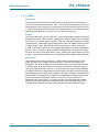
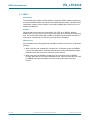
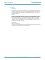
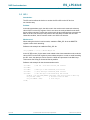
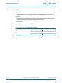
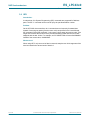
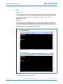
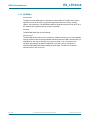
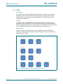
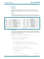
ES_LPC4370/50/30/20/10 Errata sheet LPC4370, LPC4350, LPC4330, LPC4320, LPC4310 Rev. 6.7 — 23 October 2015 Errata sheet Document information Info Content Keywords LPC4370FET100; LPC4370FET256; LPC4350FET256; LPC4350FET180; LPC4330FET256; LPC4330FET180; LPC4330FET100; LPC4330FBD144; LPC4320FET100; LPC4320FBD144; LPC4310FET100; LPC4310FBD144; Cortex-M4 flashless; Rev A, C errata Abstract This errata sheet describes both the known functional problems and any deviations from the electrical specifications known at the release date of this document. Each deviation is assigned a number and its history is tracked in a table. ES_LPC43x0 NXP Semiconductors Errata sheet LPC4370/50/30/20/10 Revision history Rev Date 6.7 20151023 6.6 20150911 6.5 20150904 6.4 20150827 6.3 20150417 6.2 20140814 6.1 20131122 6 20131021 5 20130715 4 20130125 3 20121203 2.2 Description 20120808 2.1 20120713 2 20120601 1.3 20120401 1.2 20120201 1.1 20120123 1 20120103 • • • Added RESET.3. • • • • • • • • • • • • • • • • • • • • • • • • • • • • • • Added OTP.2. Removed reference to LQFP208 package from Section 3.4 “EMC.2”. Added the word linear to the ramp-up time for the first work-around in OTP.2. For all packages, except BGA256, if the VDDREG, VDDIO, and VDDA pins are tied together, the supply voltage must have a linear ramp-up time of at least 2 ms. See Section 3.12. Added SD/MMC.1. Added EMC.2. Removed non-orderable parts LPC4350FBD208 and LPC4320FBD100. Added RESET.1. Added RESET.2. IAP.1 updated. See Section 3.6. IRC.1 removed. IRC specification changed in data sheet. Corrected retained memory location for SRAM.1 to 0x10088000. Added USBROM.2, USBROM.3, SRAM.1. Added LPC4370FET100 and LPC4370FET256. Added EMC.1, IRC.1, IDDA, USB.1, ISP.2. Renamed CDC.1 to USBROM.1. Document name changed from ES_LPC43X0_A to ES_LPC43X0. Added I2C.1. Updated C_CAN.1. Added Rev. C. Removed AES.1, ETM.1, RGU.1, SPIFI.2; documented in user manual. Added CDC.1. Updated workaround for IBAT.1. Added IBAT.2 and RGU.1. Corrected C_CAN0/C_CAN1 peripheral assignment. Added C_CAN.1. Added ISP.1, ETM.1, IAP.1, PMC.1 and IBAT.1. Updated SPIFI.1. Added SPIFI.2. Removed ADC.1 and USB0.1. Added OTP.1. Added ADC.1. Initial version. Contact information For more information, please visit: http://www.nxp.com For sales office addresses, please send an email to: [email protected] ES_LPC43X0 Errata sheet All information provided in this document is subject to legal disclaimers. Rev. 6.7 — 23 October 2015 © NXP B.V. 2015. All rights reserved. 2 of 35 ES_LPC43x0 NXP Semiconductors Errata sheet LPC4370/50/30/20/10 1. Product identification The LPC4370/50/30/20/10 devices (hereafter referred to as ‘LPC43x0’) typically have the following top-side marking: LPC43x0xxxxxx xxxxxxxx xxxYYWWxR[x] The last/second to last letter in the last line (field ‘R’) will identify the device revision. This Errata Sheet covers the following revisions of the LPC43x0: Table 1. Device revision table Revision identifier (R) Revision description ‘A’ Initial device revision ‘C’ Second device revision Field ‘YY’ states the year the device was manufactured. Field ‘WW’ states the week the device was manufactured during that year. 2. Errata overview Table 2. Functional problems table Functional problems Short description Revision identifier Detailed description BOOT.1 USB1 boot is not functional. ‘A’ Section 3.1 C_CAN.1 Writes to CAN registers write through to other peripherals. ‘A’, ‘C’ Section 3.2 EMC.1 External Memory Controller clock frequency divide by 2 ‘A’, ‘C’ mode limit. Section 3.3 EMC.2 Operating frequency of EMC lower than data sheet value. ‘A’, ‘C’ Section 3.4 I2C.1 In the slave-transmitter mode, the device set in the monitor mode must write a dummy value of 0xFF into the DAT register. ‘A’, ‘C’ Section 3.5 IAP.1 In-Application Programming API not present on flashless parts. ‘A’, ‘C’ Section 3.6 IDDA.1 Increased IDDA current in low power modes. ‘C’ Section 3.7 ISP.1 Part ID format incorrect. ‘A’, ‘C’ Section 3.8 ISP.2 ‘J’ command in ISP mode swaps last two items. ‘C’ (with a boot ROM version of 11.2) Section 3.9 MCPWM.1 MCPWM abort pin not functional. ‘A’, ‘C’ Section 3.10 OTP.1 OTP ROM driver may not program boot source. ‘A’, ‘C’ Section 3.11 OTP.2 Repeated power cycling of the device may cause erroneous programming of the OTP banks. ‘A’, ‘C’ Section 3.12 PMC.1 PMC.x power management controller fails to wake up from deep sleep, power down, or deep power down. ‘A’, ‘C’ Section 3.13 ES_LPC43X0 Errata sheet All information provided in this document is subject to legal disclaimers. Rev. 6.7 — 23 October 2015 © NXP B.V. 2015. All rights reserved. 3 of 35 ES_LPC43x0 NXP Semiconductors Errata sheet LPC4370/50/30/20/10 Table 2. Functional problems table …continued Functional problems Short description SPIFI.1 Rebooting from some SPIFI devices will be delayed by ‘A’ 60 seconds. Section 3.14 SRAM.1 Misconfigured parts. ‘A’, ‘C’ (with a date code 1315) Section 3.15 USB.1 USB0 unable to communicate with low-speed USB peripheral in host mode when using full-speed hub. ‘A’, ‘C’ Section 3.16 USBROM.1 The CDC class USB ROM drivers return a STALL condition. ‘A’ Section 3.17 USBROM.2 Nested NAK handling of EP0 OUT endpoint. ‘A’, ‘C’ Section 3.18 USBROM.3 Isochronous transfers. ‘A’, ‘C’ Section 3.19 SD/MMC.1 Data CRC error returned on CMD6 command. ‘A’, ‘C’ Section 3.20 RESET.1 Master Reset (MASTER_RST) and M4 Reset (M4_RST) are not functional. ‘A’, ‘C’ Section 3.21 RESET.2 PERIPH_RST is not functional. ‘A’, ‘C’ Section 3.22 RESET.3 Loss of device functionality on reset via nRESET in deep-sleep and power-down mode. ‘A’, ‘C’ Section 3.23 Table 3. Revision identifier Detailed description AC/DC deviations table AC/DC deviations Short description Revision identifier Detailed description IBAT.1 VBAT supply current higher than expected. ‘A’, ‘C’ Section 4.1 IBAT.2 VBAT supply current higher than expected. ‘A’ Section 4.2 PWR.1 Deep sleep and power-down mode consume more current than expected. ‘A’ Section 4.2 Table 4. Errata notes table Errata notes Short description Revision identifier Detailed description n/a n/a n/a n/a ES_LPC43X0 Errata sheet All information provided in this document is subject to legal disclaimers. Rev. 6.7 — 23 October 2015 © NXP B.V. 2015. All rights reserved. 4 of 35 ES_LPC43x0 NXP Semiconductors Errata sheet LPC4370/50/30/20/10 3. Functional problems detail 3.1 BOOT.1 Introduction: The internal ROM memory is used to store the boot code of the LPC43x0. After a reset, the ARM processor will start its code execution from this memory. The boot ROM memory includes the following features: • …Boot from USB1…. Problem: Boot from USB1 is not functional. This does not affect use of USB1 after boot-up. Work-around: USB0 can be used to boot the part. ES_LPC43X0 Errata sheet All information provided in this document is subject to legal disclaimers. Rev. 6.7 — 23 October 2015 © NXP B.V. 2015. All rights reserved. 5 of 35 ES_LPC43x0 NXP Semiconductors Errata sheet LPC4370/50/30/20/10 3.2 C_CAN.1 Introduction: Controller Area Network (CAN) is the definition of a high performance communication protocol for serial data communication. The C_CAN controller is designed to provide a full implementation of the CAN protocol according to the CAN Specification Version 2.0B. The C_CAN controller allows to build powerful local networks with low-cost multiplex wiring by supporting distributed real-time control with a very high level of security. Problem: On the LPC43x0, there is an issue with the C_CAN controller AHB bus address decoding that applies to both C_CAN controllers. It affects the C_CAN controllers when peripherals on the same bus are used. Writes to the ADC, DAC, I2C, and I2S peripherals can update registers in the C_CAN controller. Specifically, writes to I2C0, MCPWM, and I2S can affect C_CAN1. Writes to I2C1, DAC, ADC0, and ADC1 can affect C_CAN0. The spurious C_CAN controller writes will occur at the address offset written to the other peripherals on the same bus. For example, a write to ADC0 CR register which is at offset 0 in the ADC, will result in the same value being written to the C_CAN0 CNTL register which is at offset 0 in the C_CAN controller. Writes to the C_CAN controller will not affect other peripherals. Work-around: Work-arounds include: Using a different C_CAN peripheral. Peripherals I2C1, DAC, ADC0, and ADC1 can be used at the same time as C_CAN1 is active without any interference. The I2C0, MCPWM, and I2S peripherals can be used at the same time as C_CAN0 is active without any interference. Another workaround is to gate the register clock to the CAN peripheral in the CCU. This will prevent any writes to other peripherals from taking effect in the CAN peripheral. However, gating the CAN clock will prevent the CAN peripheral from operating and transmitting or receiving messages. This workaround is most useful if your application is modal and can switch between different modes such as an I2S mode and a CAN mode. Another workaround is to avoid writes to the peripherals while CAN is active. For example, the ADC could be configured to sample continuously or when triggered by a timer, before the CAN is configured. Afterwards, C_CAN0 can be used since the ADC will operate without requiring additional writes. ES_LPC43X0 Errata sheet All information provided in this document is subject to legal disclaimers. Rev. 6.7 — 23 October 2015 © NXP B.V. 2015. All rights reserved. 6 of 35 ES_LPC43x0 NXP Semiconductors Errata sheet LPC4370/50/30/20/10 3.3 EMC.1 Introduction: The LPC43x0 parts contain an External Memory Controller (EMC) capable of interfacing to external SDRAM, SRAM, and asynchronous parallel flash memories. The EMC can be configured to operate at the processor core frequency (BASE_M4_CLOCK) or the core frequency divided by 2. Problem: When operated in the divide by 2 mode (EMC_CLK_SEL, bit 16 CREG6, Address 0x4004.312C), the duty cycle of the clock is not the typical 50 % which shortens the setup time. This could impact designs with an EMC running faster than 100 MHz in divide by 2 mode (which corresponds to a maximum core frequency of 200 MHz). Work-around: If the external bus is running greater than 100 MHz in divide by 2 clock mode, consider the following: 1. When using only one external chip, use the CLK1 or CLK3 pin to drive the SDRAM clock for best performance. CLK0 and CLK2 pins are used for SDRAM read capture feedback clocks and must not be used for any other function. 2. When using two x16 SDRAMs, use the CLK1 pin to drive the clock on SDRAM D15:D0, and CLK3 pin to drive the SDRAM D31:D16. CLK0 and CLK2 pins are used for SDRAM read capture feedback clocks and must not be used for any other function. ES_LPC43X0 Errata sheet All information provided in this document is subject to legal disclaimers. Rev. 6.7 — 23 October 2015 © NXP B.V. 2015. All rights reserved. 7 of 35 ES_LPC43x0 NXP Semiconductors Errata sheet LPC4370/50/30/20/10 3.4 EMC.2 Introduction: The LPC43x0 parts contain an External Memory Controller (EMC) capable of interfacing to external SDRAM, SRAM, and asynchronous parallel flash memories. The EMC can be configured to operate at the processor core frequency (BASE_M4_CLOCK) or the core frequency divided by 2. Problem: For SDRAM, the electrical characteristic of the LQFP144 package limits the operating frequency of the EMC to a certain level, which is lower than the specified value in the data sheet. Choosing an SDRAM clock of 72MHz as the upper limit provides some safety margin. This frequency is either achieved by a core and EMC frequency of 72MHz, or by a 144MHz core and a 72MHz EMC frequency. However, SDRAM performance can vary depending on board design and layout. Work-around: There is no work-around. The upper limit of the SDRAM clock frequency is highly dependent on the PCB layout and the quality of the power supply and de-coupling circuitry. ES_LPC43X0 Errata sheet All information provided in this document is subject to legal disclaimers. Rev. 6.7 — 23 October 2015 © NXP B.V. 2015. All rights reserved. 8 of 35 ES_LPC43x0 NXP Semiconductors Errata sheet LPC4370/50/30/20/10 3.5 I2C.1 Introduction: The I2C monitor allows the device to monitor the I2C traffic on the I2C bus in a non-intrusive way. Problem: In the slave-transmitter mode, the device set in the monitor mode must write a dummy value of 0xFF into the DAT register. If this is not done, the received data from the slave device will be corrupted. To allow the monitor mode to have sufficient time to process the data on the I2C bus, the device may need to have the ability to stretch the I2C clock. Under this condition, the I2C monitor mode is not 100% non-intrusive. Work-around: When setting the device in monitor mode, enable the ENA_SCL bit in the MMCTRL register to allow clock stretching. Software code example to enable the ENA_SCL bit: LPC_I2C_MMCTRL |= (1<<1); //Enable ENA_SCL bit In the I2C ISR routine, for the status code related to the slave-transmitter mode, write the value of 0xFF into the DAT register to prevent data corruption. In order to avoid stretching the SCL clock, the data byte can be saved in a buffer and processed in the Main loop. This ensures the SI flag is cleared as fast as possible. Software code example for the slave-transmitter mode: case case case case case 0xA8: // Own SLA + R has been received, ACK returned 0xB0: 0xB8: // data byte in DAT transmitted, ACK received 0xC0: // (last) data byte transmitted, NACK received 0xC8: // last data byte in DAT transmitted, ACK received DataByte = LPC_I2C->DATA_BUFFER; //Save data. Data can be process in Main loop LPC_I2C->DAT = 0xFF; // Pretend to shift out 0xFF LPC_I2C->CONCLR = 0x08; // clear flag SI break; ES_LPC43X0 Errata sheet All information provided in this document is subject to legal disclaimers. Rev. 6.7 — 23 October 2015 © NXP B.V. 2015. All rights reserved. 9 of 35 ES_LPC43x0 NXP Semiconductors Errata sheet LPC4370/50/30/20/10 3.6 IAP.1 Introduction: The LPC43xx microcontrollers contain an API for In-Application Programming. This API also allows identification of the part. Problem: On the LPC43x0 microcontrollers, the IAP API is not present. Work-around: Use the ISP interface to identify the part ID externally (via the UART) or read the first word of the part ID directly from OTP memory at location 0x4004 5000. On flashless parts, the second word of the part ID is always 0. ES_LPC43X0 Errata sheet All information provided in this document is subject to legal disclaimers. Rev. 6.7 — 23 October 2015 © NXP B.V. 2015. All rights reserved. 10 of 35 ES_LPC43x0 NXP Semiconductors Errata sheet LPC4370/50/30/20/10 3.7 IDDA.1 Introduction: This part includes two 10-bit analog to digital converters that require a 3.3 V supply. Problem: While in deep sleep and power-down modes, analog domains show increased current. The table below shows the actual power drawn in these modes. Work-around: None. Table 5. Static characteristics Tamb = 40 C to +85C, unless otherwise specified Symbol IDDA [1] ES_LPC43X0 Errata sheet Parameter Conditions Min Typ Max Unit [1] - 4.2 - A power-down mode [1] - 4.2 - A deep power-down mode [1] - 0.007 - A analog supply current deep sleep mode VDDA(3V3) = 3.3 V; Tamb = 25C. All information provided in this document is subject to legal disclaimers. Rev. 6.7 — 23 October 2015 © NXP B.V. 2015. All rights reserved. 11 of 35 ES_LPC43x0 NXP Semiconductors Errata sheet LPC4370/50/30/20/10 3.8 ISP.1 Introduction: A reduced set of In-System-Programming (ISP) commands are supported for flashless parts. The ISP 'J' command can be used to query the part identification number. Problem: On the LPC43x0 microcontrollers, the J command returns incorrectly formatted data. Instead of returning two words (plus the return code) as specified in the User's Manual, IAP command 54 and ISP command 'J' only return a single word (plus return code). That single word contains the first word of the part identification number with the first 16 bits swapped with the last 16 bits. For example, an LPC4350FET256 will return 0x0830A000 instead of the correct value, 0xA0000830. Work-around: When using ISP, if only one word of data is returned, swap the two 16-bit segments of the word and assume the second word of data is 0. ES_LPC43X0 Errata sheet All information provided in this document is subject to legal disclaimers. Rev. 6.7 — 23 October 2015 © NXP B.V. 2015. All rights reserved. 12 of 35 ES_LPC43x0 NXP Semiconductors Errata sheet LPC4370/50/30/20/10 3.9 ISP.2 Introduction: All LPC43x0 parts include a feature called In-System Programming (ISP) which boots up over the UART port and provides a terminal-based communication mechanism to query certain characteristics of the part. One of these is the ability to retrieve the Part Identification number. Problem: The 'J' command in ISP mode should return an error code, followed by an ASCII string representation of the part ID, followed by a 0. However what is actually returned is the error code, followed by a 0, followed by an ASCII string representation of the part ID. The problem is the last two items returned are swapped. Incorrect example: Correct example: Work-around: There is no work-around for this problem. ES_LPC43X0 Errata sheet All information provided in this document is subject to legal disclaimers. Rev. 6.7 — 23 October 2015 © NXP B.V. 2015. All rights reserved. 13 of 35 ES_LPC43x0 NXP Semiconductors Errata sheet LPC4370/50/30/20/10 3.10 MCPWM.1 Introduction: The Motor Control PWM engine is optimized for three-phase AC and DC motor control applications, but can be used in many other applications that need timing, counting, capture, and comparison. The MCPWM contains a global Abort input that can force all of the channels into a passive state and cause an interrupt. Problem: The MCPWM Abort input is not functional. Work-around: The MCPWM Abort function can be emulated in software with the use of a non-maskable interrupt combined with an interrupt handler that shuts down the PWM. This will result in a small delay on the order of 50 main clock cycles or about 1/3 of a microsecond at 150 MHz. Alternatively, the State Configurable Timer (SCT) can be configured to implement MCPWM functionality including an Abort input. The SCT can respond to external inputs in one clock cycle. ES_LPC43X0 Errata sheet All information provided in this document is subject to legal disclaimers. Rev. 6.7 — 23 October 2015 © NXP B.V. 2015. All rights reserved. 14 of 35 ES_LPC43x0 NXP Semiconductors Errata sheet LPC4370/50/30/20/10 3.11 OTP.1 Introduction: The LPC43x0 contain OTP memory which can configure the boot source, as well as a set of routines in ROM to program the boot source into OTP memory. Problem: There is a problem in the OTP boot source programming code in ROM which requires registers to be initialized in order to ensure successful boot source OTP programming. Work-around: 1. Add this function to your program. void OTP_fix(volatile unsigned dummy0,volatile unsigned dummy1,volatile unsigned dummy2,volatile unsigned dummy3) { } 2. Call this function before calling otp_ProgBootSrc. rval = otp_Init(); OTP_fix(0,0,0,0); rval = otp_ProgBootSrc(OTP_BOOTSRC_SPIFI); This will be fixed in the next boot ROM revision. ES_LPC43X0 Errata sheet All information provided in this document is subject to legal disclaimers. Rev. 6.7 — 23 October 2015 © NXP B.V. 2015. All rights reserved. 15 of 35 ES_LPC43x0 NXP Semiconductors Errata sheet LPC4370/50/30/20/10 3.12 OTP.2 Introduction: The LPC43x0 parts contain OTP memory with four banks of 128 bits each. The first bank (OTP bank 0) is reserved. The other three OTP banks are programmable. The OTP banks can be programmed (0 1) via APIs provided in the ROM. Problem: On all packages, repeated power cycling of the device may cause erroneous programming of the OTP banks. During ramp-up, the VDDREG supply voltage does not have enough time to settle and initialize the OTP controller before valid programming voltage is reached on the VPP pin. This may cause accidental programming of the OTP banks. Accidental programming of the OTP banks does not occur during Power-down of the supply voltage. Work-around: There are two possible work-arounds to avoid accidental programming of the OTP banks: 1. Ensure supply ramp-up time of 2 ms or greater: a. For all packages, except BGA256, if the VDDREG, VDDIO, and VDDA pins are tied together, the supply voltage must have a linear ramp-up time of at least 2 ms. If the VDDREG, VDDA, and VDDIO pins are not tied together, follow the work-around in List item 2 “Delay VDDIO and RESETN pin:” b. On the BGA256 package, if OTP programming is required, the voltage on the VPP pin should be delayed by 2 ms after the power supply on the VDDREG, VDDA, and VDDIO pins reaches the operating voltage level. If the VPP pin is tied to VDDREG, VDDA, and VDDIO pins, the supply voltage must have a linear ramp-up time of at least 2 ms. If OTP programming is not required on the BGA256 package, the VPP pin should be left as No-Connect (NC) because the VPP and VDDIO pins are separate. 2. Delay VDDIO and RESETN pin: The power supplied to the VDDIO pin should be delayed by 2 ms after the power supply on the VDDREG and VDDA pins stabilizes at the operating voltage level. If booting from external sources (USARTx, SPIFI, EMC, USBx, SPI), the signal to the RESETN pin must also be delayed by 2 ms after the power supply on the VDDIO pin stabilizes at the operating voltage level. The following circuit diagram is an example that shows the P-channel MOSFET with the gate delayed and the R-C delay circuit connected to the RESETN pin. ES_LPC43X0 Errata sheet All information provided in this document is subject to legal disclaimers. Rev. 6.7 — 23 October 2015 © NXP B.V. 2015. All rights reserved. 16 of 35 ES_LPC43x0 NXP Semiconductors Errata sheet LPC4370/50/30/20/10 For this problem, there is no restriction on the VBAT supply. The following diagram shows the waveform for the work-around in List item 2 “Delay VDDIO and RESETN pin:” ES_LPC43X0 Errata sheet All information provided in this document is subject to legal disclaimers. Rev. 6.7 — 23 October 2015 © NXP B.V. 2015. All rights reserved. 17 of 35 ES_LPC43x0 NXP Semiconductors Errata sheet LPC4370/50/30/20/10 3.13 PMC.1 Introduction: The PMC implements the control sequences to enable transitions between different power modes and controls the power state of each peripheral. In addition, wake-up from any of the power-down modes based on hardware events is supported. Problem: When the chip is in a transition from active to deep Sleep, power down, or deep power down, wake-up events are not captured and they will block further wake-up events from propagating. The time window for this transition is 6 uS and is not affected by the chip clock speed. After a wake-up event is received during the PMC transition, the chip can only recover by using an external hardware reset or by cycling power. Work-around: Make sure that a wake-up signal is not received during the deep sleep, power down, or deep power down transition period. An example circuit to work around this could include an external 6 S one shot which could be triggered via software using a GPIO line when entering deep sleep, power down, or deep power down mode. The one-shot's output could be used to gate the wake-up signal(s) to prevent receiving a wake-up signal during the PMC transition period. Depending on the system design, it may also be needed to latch the wake-up signal(s) so that they will still be present after the one-shot's 6 S time-out. Run mode PMC transition period 6 us PMC state Keep-out area Low power mode PMC software trigger Wakeup signal asserted (ok) Fig 1. ES_LPC43X0 Errata sheet PMC wake-up keep-out area All information provided in this document is subject to legal disclaimers. Rev. 6.7 — 23 October 2015 © NXP B.V. 2015. All rights reserved. 18 of 35 ES_LPC43x0 NXP Semiconductors Errata sheet LPC4370/50/30/20/10 3.14 SPIFI.1 Introduction: The boot ROM includes a SPI Flash Interface (SPIFI) driver that allows low-cost serial flash memories to be connected to the ARM Cortex-M4 processor with little performance penalty compared to parallel flash devices with higher pin count. SPIFI provides a memory-mapped area where the contents of the external serial flash memory appear. Problem: The boot ROM does not properly re-initialize the external serial flash device if it is already set up for "no opcode" or "continuous read" mode. This affects use after unplanned resets such as a hardware reset or watchdog timer reset. Booting from SPIFI is affected and may not be successful until after the 60 second boot failure time-out if the external serial flash device is in "no opcode" or "continuous read" mode. Work-around: During a planned reboot, remove the external QSPI flash from no opcode mode before resetting the CPU by using the SPIFI driver library's cancel_mem_mode call. The SPIFI driver library is available from lpcware.com. In the event of an unplanned reset, the driver will initialize the flash device if it is called a second time so an external watchdog could be provided to reset the CPU in case of boot failure from SPIFI. Finally there is a built-in 60-second boot time-out which will result in a successful boot after one minute in the event of a failure. ES_LPC43X0 Errata sheet All information provided in this document is subject to legal disclaimers. Rev. 6.7 — 23 October 2015 © NXP B.V. 2015. All rights reserved. 19 of 35 ES_LPC43x0 NXP Semiconductors Errata sheet LPC4370/50/30/20/10 3.15 SRAM.1 Introduction: The LPC4320/10 parts all have an 8 kB region of internal SRAM that is retained during Sleep, deep-sleep, and power-down modes. This retained memory is located at 0x10088000. Problem: Parts with date codes marked 1315 locate the 8 kB of retained memory at 0x10090000. Also, the part numbers for these parts returned by the ISP Read Part Identification command is incorrect. The correct part numbers look like this: Fig 2. ES_LPC43X0 Errata sheet Correct part numbers All information provided in this document is subject to legal disclaimers. Rev. 6.7 — 23 October 2015 © NXP B.V. 2015. All rights reserved. 20 of 35 ES_LPC43x0 NXP Semiconductors Errata sheet LPC4370/50/30/20/10 The misconfigured parts discussed in this errata have part numbers that look like this: Fig 3. Misconfigured part numbers Work-around: There is no way to change the memory configuration of these parts. However it is advised that software check the value of the part number returned from the ISP Read Part Identification command and take the appropriate action based on what value is read. If bit 14 equals 0 then the part is misconfigured as described in this errata. ES_LPC43X0 Errata sheet All information provided in this document is subject to legal disclaimers. Rev. 6.7 — 23 October 2015 © NXP B.V. 2015. All rights reserved. 21 of 35 ES_LPC43x0 NXP Semiconductors Errata sheet LPC4370/50/30/20/10 3.16 USB.1 Introduction: The LPC43x0 parts include two USB 2.0 controllers that can operate in host mode at high-speed. One of these controllers, USB0, contains an on-chip high-speed UTMI+ compliant transceiver (PHY) which supports high-speed, full-speed, and low-speed USB-compliant peripherals. Problem: The USB controller called USB0 is unable to communicate with a low-speed USB peripheral in host mode when there is a full-speed hub directly connected to the USB0 port and a low-speed peripheral is connected in the tree somewhere below this full-speed hub. Only USB0 has this problem; the other USB controller, USB1 does not. Work-around: There is no work-around for this problem. It is suggested that the low-speed USB peripheral is either connected directly to USB0 or a high-speed hub is placed between that peripheral and USB0. Fig 4. ES_LPC43X0 Errata sheet Suggested USB0 to low-speed peripheral connections All information provided in this document is subject to legal disclaimers. Rev. 6.7 — 23 October 2015 © NXP B.V. 2015. All rights reserved. 22 of 35 ES_LPC43x0 NXP Semiconductors Errata sheet LPC4370/50/30/20/10 3.17 USBROM.1 Introduction: The CDC class USB ROM drivers have a bug that causes some Windows terminal emulation programs like Hyperterm to fail to connect. This bug only exists in revision 'A' parts. Problem: The CDC class USB ROM drivers return a STALL condition after the DATA stage of a Set Line Coding CONTROL transfer from the host. The correct behavior is to return an ACK. Fig 5. Incorrect Fig 6. Correct Work-around: The way to work around this bug is to override the default CDC class specific endpoint 0 handler and handle the processing of OUT packets in your application. Use the following source code in red to accomplish this. USB_EP_HANDLER_T g_defaultCdcHdlr; // default CDC handler ErrorCode_t CDC_ep0_override_hdlr(USBD_HANDLE_T hUsb, void* data, uint32_t event) { USB_CORE_CTRL_T* pCtrl = (USB_CORE_CTRL_T*)hUsb; USB_CDC_CTRL_T* pCdcCtrl = (USB_CDC_CTRL_T*) data; ErrorCode_t ret = ERR_USBD_UNHANDLED; if( (event == USB_EVT_OUT) && (pCtrl->SetupPacket.bmRequestType.BM.Type == REQUEST_CLASS) && (pCtrl->SetupPacket.bmRequestType.BM.Recipient == REQUEST_TO_INTERFACE) && ((pCtrl->SetupPacket.wIndex.WB.L == pCdcCtrl->cif_num) || /* IF number correct? */ (pCtrl->SetupPacket.wIndex.WB.L == pCdcCtrl->dif_num)) ) { pCtrl->EP0Data.pData -= pCtrl->SetupPacket.wLength; ret = pCdcCtrl->CIC_SetRequest(pCdcCtrl, &pCtrl->SetupPacket, &pCtrl->EP0Data.pData, pCtrl->SetupPacket.wLength); if ( ret == LPC_OK) { USBD_API->core->StatusInStage(pCtrl); /* send Acknowledge */ } ES_LPC43X0 Errata sheet All information provided in this document is subject to legal disclaimers. Rev. 6.7 — 23 October 2015 © NXP B.V. 2015. All rights reserved. 23 of 35 ES_LPC43x0 NXP Semiconductors Errata sheet LPC4370/50/30/20/10 } else { ret = g_defaultCdcHdlr(hUsb, data, event); } return ret; } void UsbdCdc_Init(void) { . . . USBD_API->cdc->init(UsbHandle, &cdc_param, &UsbdCdcHdlr); { // This code must be placed immediately after the call to USBD_API->cdc->init() USB_CORE_CTRL_T* pCtrl = (USB_CORE_CTRL_T*)UsbHandle; /* store the default CDC handler and replace it with ours */ g_defaultCdcHdlr = pCtrl->ep0_hdlr_cb[pCtrl->num_ep0_hdlrs - 1]; pCtrl->ep0_hdlr_cb[pCtrl->num_ep0_hdlrs - 1] = CDC_ep0_override_hdlr; } } ES_LPC43X0 Errata sheet All information provided in this document is subject to legal disclaimers. Rev. 6.7 — 23 October 2015 © NXP B.V. 2015. All rights reserved. 24 of 35 ES_LPC43x0 NXP Semiconductors Errata sheet LPC4370/50/30/20/10 3.18 USBROM.2 Introduction: The USB ROM drivers include a default endpoint 0 handler which acts on events generated by the USB controller as a result of traffic occurring over the control endpoint. The user has the option of overloading this default handler for the purpose of performing user specific processing of control endpoint traffic as required. One of the actions the default endpoint 0 handler performs is to prepare the DMA engine for data transfer after the controller has sent out a NAK packet to the host controller. This is done in preparation for the arrival of the next OUT request received from the host. Problem: Due to a race condition there is the chance that a second NAK event will occur before the default endpoint0 handler has completed its preparation of the DMA engine for the first NAK event. This can cause certain fields in the DMA descriptors to be in an invalid state when the USB controller reads them, thereby causing a hang. Work-around: Override the default endpoint 0 handler to add checks for and prevents nested NAK event processing activity. This is an example of how to do this: // Endpoint 0 patch that prevents nested NAK event processing static uint32_t g_ep0RxBusy = 0; /* flag indicating whether EP0 OUT/RX buffer is busy. */ static USB_EP_HANDLER_T g_Ep0BaseHdlr; /* variable to store the pointer to base EP0 handler */ /*---------------------------------------------------------------------------EP0_patch : *----------------------------------------------------------------------------*/ ErrorCode_t EP0_patch(USBD_HANDLE_T hUsb, void* data, uint32_t event) { switch (event) { case USB_EVT_OUT_NAK: if (g_ep0RxBusy) { /* we already queued the return LPC_OK; } else { /* Mark EP0_RX buffer as buffer. */ g_ep0RxBusy = 1; } break; case USB_EVT_SETUP: /* reset the case USB_EVT_OUT: /* we received the packet so g_ep0RxBusy = 0; ES_LPC43X0 Errata sheet buffer so ignore this NAK event. */ busy and allow base handler to queue the flag when new setup sequence starts */ clear the flag. */ All information provided in this document is subject to legal disclaimers. Rev. 6.7 — 23 October 2015 © NXP B.V. 2015. All rights reserved. 25 of 35 ES_LPC43x0 NXP Semiconductors Errata sheet LPC4370/50/30/20/10 break; } return g_Ep0BaseHdlr(hUsb, data, event); } // Install the endpoint 0 patch immediately after USB initialization via the hw->Init() call. *---------------------------------------------------------------------------usbd_init: usb subsystem init routine *----------------------------------------------------------------------------*/ ErrorCode_t usbd_init (void) { USBD_API_INIT_PARAM_T usb_param; USB_CORE_DESCS_T desc; ErrorCode_t ret = LPC_OK; USB_CORE_CTRL_T* pCtrl; … /* USB Initialization */ ret = USBD_API->hw->Init(&g_AdcCtrl.hUsb, &desc, &usb_param); if (ret == LPC_OK) { /* register EP0 patch */ pCtrl= (USB_CORE_CTRL_T*)g_AdcCtrl.hUsb; /* convert the handle to control structure */ g_Ep0BaseHdlr = pCtrl->ep_event_hdlr[0]; /* retrieve the default EP0_OUT handler */ pCtrl->ep_event_hdlr[0] = EP0_patch; /* set our patch routine as EP0_OUT handler */ …. } …. return LPC_OK; } ES_LPC43X0 Errata sheet All information provided in this document is subject to legal disclaimers. Rev. 6.7 — 23 October 2015 © NXP B.V. 2015. All rights reserved. 26 of 35 ES_LPC43x0 NXP Semiconductors Errata sheet LPC4370/50/30/20/10 3.19 USBROM.3 Introduction: The USB ROM drivers configure and manage data structures used by the USB controller's DMA engine to move data between the controller's internal fifos and system memory. The configuration of these data structures are based on many parameters including the type of transfer, control, bulk, interrupt, or isochronous, that is to be performed. These data structures reside in system RAM on a 2 kB boundary and are pointed to by the ENDPOINTLISTADDR register. Problem: The USB ROM drivers incorrectly configures the Endpoint Capabilities/Characteristics field of the device Queue Head (dQH) structure for isochronous endpoints. Specifically, the MULT member is set to 0 and the ZLT member is set to 1. Also if the maximum size of isochronous packets are 1024 bytes the Max_packet_length member will be set to 0. For any other packet size this member is set correctly. Work-around: To use isochronous transfers with the USB ROM drivers the Endpoint Capabilities/Characteristics field must be correctly configured for that endpoint's device Queue Head structure. The USB ROM driver always sets this field (incorrectly) when the host sends a Set Interface control packet and then it calls the USB_Interface_Event callback routine, so the field must be set with the proper value in this callback routine. This is the device Queue Head structure: typedef volatile struct { volatile uint32_t cap; volatile uint32_t curr_dTD; volatile uint32_t next_dTD; volatile uint32_t total_bytes; volatile uint32_t buffer0; volatile uint32_t buffer1; volatile uint32_t buffer2; volatile uint32_t buffer3; volatile uint32_t buffer4; volatile uint32_t reserved; volatile uint32_t setup[2]; volatile uint32_t gap[4]; } DQH_T; This is an Interface Event callback routine: ErrorCode_t USB_Interface_Event (USBD_HANDLE_T hUsb) { USB_CORE_CTRL_T* pCtrl = (USB_CORE_CTRL_T*)hUsb; uint16_t wIndex = pCtrl->SetupPacket.wIndex.W; // Interface number uint16_t wValue = pCtrl->SetupPacket.wValue.W; // Alternate setting number if (wIndex == isochronous_interface_number && wValue == 1) { ES_LPC43X0 Errata sheet All information provided in this document is subject to legal disclaimers. Rev. 6.7 — 23 October 2015 © NXP B.V. 2015. All rights reserved. 27 of 35 ES_LPC43x0 NXP Semiconductors Errata sheet LPC4370/50/30/20/10 DQH_T* ep_QH = *(DQH_T**)0x40006158; // ENDPOINTLISTADDR register int QH_idx = ((endpoint_address & 0x0F) << 1) + 1; ep_QH[QH_idx].cap = ((packets_executed_per_transaction_descriptor << 30) | (maximum_packet_size << 16)); } return LPC_OK; } The value of isochronous_interface_number should correspond to the interface number in the USB descriptor that holds the isochronous endpoint you wish to use. The value of maximum_packet_size should correspond to the wMaxPacketSize member of the isochronous endpoint descriptor The value of endpoint_address should correspond to the bEndpointAddress member of the isochronous endpoint descriptor ES_LPC43X0 Errata sheet All information provided in this document is subject to legal disclaimers. Rev. 6.7 — 23 October 2015 © NXP B.V. 2015. All rights reserved. 28 of 35 ES_LPC43x0 NXP Semiconductors Errata sheet LPC4370/50/30/20/10 3.20 SD/MMC.1 Introduction: The LPC43x0 parts have the SD/MMC interface. After power up, the SD memory card is in the default speed mode, and by using the Switch Function command (CMD6), Version 1.10 and higher, the SD memory cards can be placed in high-speed mode. In response to the CMD6 command, the SD card returns a 512-bit block of data containing the available features and actual settings. The SDIO interface is setup for 4-bit data and therefore, the 512 bits are returned on the four data lines in 128 clocks followed by 16 clocks of CRC data. Problem: The CMD6 returned status block always gets a data CRC error although the status data is correct. The data CRC error prevents the switching of the SD memory card from the default mode to high-speed mode. Work-around: Capture the 64 bits of CRC data that follow the 512 bits of data allowing the CRC data to be calculated in software. The DMA buffer length and SD/MMC BYTCNT must be set to 72 (versus 64). The CRC data consists of four interleaved 16-bit words, one for each of the four serialized SD data bits. If all four of the calculated CRCs match the captured CRCs, the software can clear the data CRC error flag bit. ES_LPC43X0 Errata sheet All information provided in this document is subject to legal disclaimers. Rev. 6.7 — 23 October 2015 © NXP B.V. 2015. All rights reserved. 29 of 35 ES_LPC43x0 NXP Semiconductors Errata sheet LPC4370/50/30/20/10 3.21 RESET.1 Introduction: The LPC43x0 parts contain a Reset Generation Unit (RGU) that generates various resets; Core Reset (CORE_RST), Peripheral Reset (PERIPH_RST), Master Reset (MASTER_RST), and M4 Reset (M4_RST). Problem: On the LPC43x0, MASTER_RST and M4_RST are not functional. Work-around: There is no work-around. To reset the entire chip use the CORE_RST instead of using MASTER_RST or M4_RST. ES_LPC43X0 Errata sheet All information provided in this document is subject to legal disclaimers. Rev. 6.7 — 23 October 2015 © NXP B.V. 2015. All rights reserved. 30 of 35 ES_LPC43x0 NXP Semiconductors Errata sheet LPC4370/50/30/20/10 3.22 RESET.2 Introduction: The LPC43x0 parts contain a Reset Generation Unit (RGU) that generates various resets; Core Reset (CORE_RST), Peripheral Reset (PERIPH_RST), Master Reset (MASTER_RST), and M4 Reset (M4_RST). Problem: On the LPC43x0, PERIPH_RST is not functional. CMSIS call NVIC_SystemReset() uses PERIPH_RST internally and is also non-functional. Work-around: There is no work-around. To reset the entire chip, use the CORE_RST instead of using CMSIS call NVIC_SystemReset() or PERIPH_RST. ES_LPC43X0 Errata sheet All information provided in this document is subject to legal disclaimers. Rev. 6.7 — 23 October 2015 © NXP B.V. 2015. All rights reserved. 31 of 35 ES_LPC43x0 NXP Semiconductors Errata sheet LPC4370/50/30/20/10 3.23 RESET.3 Introduction: The LPC43x0 devices are initialized after a reset. If a reset occurs via nRESET pin when the part is in deep-sleep or power-down mode, the initialization state of the device may be erroneous and some functionality of the device may be lost. Problem: When the part is in deep-sleep or power-down mode and if an external reset occurs via nRESET pin being activated, as the part comes out of reset, the reset state of some functional blocks may be incorrect. This may result in loss of functionality of the device. The actual functionality lost may vary from part to part depending on the erroneous reset state of the functional blocks. The possible affected blocks are: Ethernet, LCD controller, CAN0, CAN1, USB0, USB1, SGPIO, AES, Cortex-M0 coprocessor and Cortex-M0 subsystem (if present), 12-bit ADC, SRAM size at 0x1000 0000 may change to 32 kB, SRAM size at 0x1008 0000 may change to 40 kB, SRAM size at 0x2000 0000 may change to 16 kB, SRAM size at 0x2000 8000 may change to 0 kB, and SRAM size at 0x2000 C000 may change to 0 kB. Work-around: There are two possible work-arounds: 1. In the application software, before initializing peripherals, the code should assert a soft reset using the following steps: a. Read the value in Power-down modes register (PD0_SLEEP0_MODE). b. If the value in the PD0_SLEEP0_MODE0 register represents deep-sleep mode or power-down mode, then the user should check if a reset event occurred on the nRESET pin (bit ‘19’ in the Event Status register). c. If the reset event occurred, the software should set the PD0_SLEEP0_MODE register to deep power-down mode and assert a soft reset using the CORE_RST (bit ‘0’ in the RESET_CTRL0 register). /* Check if wake up event happens in deep sleep or power down mode */ if((LPC_PMC->PD0_SLEEP0_MODE == PMC_PWR_DEEP_SLEEP_MODE) || (LPC_PMC->PD0_SLEEP0_MODE == PMC_PWR_POWER_DOWN_MODE)) { /* Check if the wake up event is due to nRESET pin in Event router */ if(LPC_EVRT->STATUS & (1<<19)) { /* Set power state in PMC */ LPC_PMC->PD0_SLEEP0_MODE = PMC_PWR_DEEP_POWER_DOWN_MODE; /* Set CORE_RST in RGU */ LPC_RGU->RESET_CTRL0 = (1<<0); } } 2. To initialize the device correctly, assert a second external reset signal to the nRESET pin after 20 s from the first reset. ES_LPC43X0 Errata sheet All information provided in this document is subject to legal disclaimers. Rev. 6.7 — 23 October 2015 © NXP B.V. 2015. All rights reserved. 32 of 35 ES_LPC43x0 NXP Semiconductors Errata sheet LPC4370/50/30/20/10 4. AC/DC deviations detail 4.1 IBAT.1 Introduction: The LPC43x0 contain a Real-Time Clock which measures the passage of time. The RTC has an ultra-low power design to support battery powered systems with a dedicated battery supply pin. Problem: On the LPC43x0, high current consumption of about 70 A may occur on the VBAT power supply pin. Work-around: VBAT current consumption can be lowered significantly by configuring the RTC_ALARM pin as "Inactive" by setting the ALARMCTRL 7:6 field in CREG0 to 0x3. These bits persist through power cycles and reset while VBAT is present. For CREG0[13:12] reserved value 0x3 should be used; this value should be set once after a power on reset. 4.2 IBAT.2 Introduction: The LPC43x0 contain a Real-Time Clock which measures the passage of time. The RTC has an ultra-low power design to support battery powered systems with a dedicated battery supply pin. Problem: On the LPC43x0, high current consumption of about 15 A may occur on the VBAT power supply pin despite applying the workaround in IBAT.1. Work-around: The problem is caused by a design error and there is currently no work-around. 4.3 PWR.1 Introduction: The LPC43x0 contain several low-power modes. The PMC implements the control sequences to enable transitions between different power modes and controls the power state of each peripheral. Problem: A design error results in about 15 A higher current consumption during deep-sleep and power-down mode. Work-around: None. ES_LPC43X0 Errata sheet All information provided in this document is subject to legal disclaimers. Rev. 6.7 — 23 October 2015 © NXP B.V. 2015. All rights reserved. 33 of 35 ES_LPC43x0 NXP Semiconductors Errata sheet LPC4370/50/30/20/10 5. Legal information 5.1 Definitions Draft — The document is a draft version only. The content is still under internal review and subject to formal approval, which may result in modifications or additions. NXP Semiconductors does not give any representations or warranties as to the accuracy or completeness of information included herein and shall have no liability for the consequences of use of such information. 5.2 Disclaimers Limited warranty and liability — Information in this document is believed to be accurate and reliable. However, NXP Semiconductors does not give any representations or warranties, expressed or implied, as to the accuracy or completeness of such information and shall have no liability for the consequences of use of such information. NXP Semiconductors takes no responsibility for the content in this document if provided by an information source outside of NXP Semiconductors. In no event shall NXP Semiconductors be liable for any indirect, incidental, punitive, special or consequential damages (including - without limitation - lost profits, lost savings, business interruption, costs related to the removal or replacement of any products or rework charges) whether or not such damages are based on tort (including negligence), warranty, breach of contract or any other legal theory. Notwithstanding any damages that customer might incur for any reason whatsoever, NXP Semiconductors’ aggregate and cumulative liability towards customer for the products described herein shall be limited in accordance with the Terms and conditions of commercial sale of NXP Semiconductors. Right to make changes — NXP Semiconductors reserves the right to make changes to information published in this document, including without limitation specifications and product descriptions, at any time and without notice. This document supersedes and replaces all information supplied prior to the publication hereof. Suitability for use — NXP Semiconductors products are not designed, authorized or warranted to be suitable for use in life support, life-critical or safety-critical systems or equipment, nor in applications where failure or ES_LPC43X0 Errata sheet malfunction of an NXP Semiconductors product can reasonably be expected to result in personal injury, death or severe property or environmental damage. NXP Semiconductors and its suppliers accept no liability for inclusion and/or use of NXP Semiconductors products in such equipment or applications and therefore such inclusion and/or use is at the customer’s own risk. Applications — Applications that are described herein for any of these products are for illustrative purposes only. NXP Semiconductors makes no representation or warranty that such applications will be suitable for the specified use without further testing or modification. Customers are responsible for the design and operation of their applications and products using NXP Semiconductors products, and NXP Semiconductors accepts no liability for any assistance with applications or customer product design. It is customer’s sole responsibility to determine whether the NXP Semiconductors product is suitable and fit for the customer’s applications and products planned, as well as for the planned application and use of customer’s third party customer(s). Customers should provide appropriate design and operating safeguards to minimize the risks associated with their applications and products. NXP Semiconductors does not accept any liability related to any default, damage, costs or problem which is based on any weakness or default in the customer’s applications or products, or the application or use by customer’s third party customer(s). Customer is responsible for doing all necessary testing for the customer’s applications and products using NXP Semiconductors products in order to avoid a default of the applications and the products or of the application or use by customer’s third party customer(s). NXP does not accept any liability in this respect. Export control — This document as well as the item(s) described herein may be subject to export control regulations. Export might require a prior authorization from competent authorities. 5.3 Trademarks Notice: All referenced brands, product names, service names and trademarks are the property of their respective owners. All information provided in this document is subject to legal disclaimers. Rev. 6.7 — 23 October 2015 © NXP B.V. 2015. All rights reserved. 34 of 35 ES_LPC43x0 NXP Semiconductors Errata sheet LPC4370/50/30/20/10 6. Contents 1 2 3 3.1 3.2 3.3 3.4 3.5 3.6 3.7 3.8 3.9 3.10 3.11 3.12 3.13 3.14 3.15 3.16 3.17 3.18 3.19 3.20 3.21 3.22 3.23 4 4.1 4.2 4.3 5 5.1 5.2 5.3 6 Product identification . . . . . . . . . . . . . . . . . . . . 3 Errata overview . . . . . . . . . . . . . . . . . . . . . . . . . 3 Functional problems detail . . . . . . . . . . . . . . . . 5 BOOT.1 . . . . . . . . . . . . . . . . . . . . . . . . . . . . . . . 5 C_CAN.1 . . . . . . . . . . . . . . . . . . . . . . . . . . . . . 6 EMC.1. . . . . . . . . . . . . . . . . . . . . . . . . . . . . . . . 7 EMC.2. . . . . . . . . . . . . . . . . . . . . . . . . . . . . . . . 8 I2C.1 . . . . . . . . . . . . . . . . . . . . . . . . . . . . . . . . . 9 IAP.1 . . . . . . . . . . . . . . . . . . . . . . . . . . . . . . . . 10 IDDA.1 . . . . . . . . . . . . . . . . . . . . . . . . . . . . . . 11 ISP.1 . . . . . . . . . . . . . . . . . . . . . . . . . . . . . . . . 12 ISP.2 . . . . . . . . . . . . . . . . . . . . . . . . . . . . . . . . 13 MCPWM.1 . . . . . . . . . . . . . . . . . . . . . . . . . . . 14 OTP.1 . . . . . . . . . . . . . . . . . . . . . . . . . . . . . . . 15 OTP.2 . . . . . . . . . . . . . . . . . . . . . . . . . . . . . . . 16 PMC.1. . . . . . . . . . . . . . . . . . . . . . . . . . . . . . . 18 SPIFI.1 . . . . . . . . . . . . . . . . . . . . . . . . . . . . . . 19 SRAM.1 . . . . . . . . . . . . . . . . . . . . . . . . . . . . . 20 USB.1 . . . . . . . . . . . . . . . . . . . . . . . . . . . . . . . 22 USBROM.1 . . . . . . . . . . . . . . . . . . . . . . . . . . . 23 USBROM.2 . . . . . . . . . . . . . . . . . . . . . . . . . . . 25 USBROM.3 . . . . . . . . . . . . . . . . . . . . . . . . . . . 27 SD/MMC.1 . . . . . . . . . . . . . . . . . . . . . . . . . . . 29 RESET.1 . . . . . . . . . . . . . . . . . . . . . . . . . . . . . 30 RESET.2 . . . . . . . . . . . . . . . . . . . . . . . . . . . . . 31 RESET.3 . . . . . . . . . . . . . . . . . . . . . . . . . . . . . 32 AC/DC deviations detail . . . . . . . . . . . . . . . . . 33 IBAT.1 . . . . . . . . . . . . . . . . . . . . . . . . . . . . . . . 33 IBAT.2 . . . . . . . . . . . . . . . . . . . . . . . . . . . . . . . 33 PWR.1 . . . . . . . . . . . . . . . . . . . . . . . . . . . . . . 33 Legal information. . . . . . . . . . . . . . . . . . . . . . . 34 Definitions . . . . . . . . . . . . . . . . . . . . . . . . . . . . 34 Disclaimers . . . . . . . . . . . . . . . . . . . . . . . . . . . 34 Trademarks. . . . . . . . . . . . . . . . . . . . . . . . . . . 34 Contents . . . . . . . . . . . . . . . . . . . . . . . . . . . . . . 35 Please be aware that important notices concerning this document and the product(s) described herein, have been included in section ‘Legal information’. © NXP B.V. 2015. All rights reserved. For more information, please visit: http://www.nxp.com For sales office addresses, please send an email to: [email protected] Date of release: 23 October 2015 Document identifier: ES_LPC43X0