1
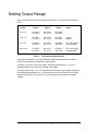
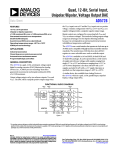
IP-16DAC
Three Channel 16-bit Digital to Analog
Converter for Instrumentation
IndustryPack™
User Manual
©SBS Technologies, Inc.
Subject to change without notice.
Part No. 89006170 Rev.1.0 20040914
Hardware Revision: C2
IP-16DAC
Three Channel Digital to Analog
Converter for Instrumentation
IndustryPack™
SBS Technologies, Inc.
1284 Corporate Center Drive
St. Paul, MN 55121-1245
Tel: (651) 905-4700
FAX: (651) 905-4701
www.sbs.com
©1999-2004 SBS Technologies, Inc.
IndustryPack is a registered trademark of SBS
Technologies, Inc. QuickPack, SDpacK and Unilin
are trademarks SBS Technologies, Inc. PC•MIP is a
trademark of SBS Technologies, Inc. and MEN
Micro Electronics.
SBS Technologies, Inc. acknowledges the
trademarks of other organizations for their respective
products mentioned in this document.
All rights are reserved. No one is permitted to
reproduce or duplicate, in any form, the whole or part
of this document without the express consent of SBS
Technologies, Inc.. This document is meant solely
for the purpose in which it was delivered.
SBS Technologies, Inc. reserves the right to make
any changes in the devices or device specifications
contained herein at any time and without notice.
Customers are advised to verify all information
contained in this document.
The electronic equipment described herein
generates, uses and may radiate radio frequency
energy, which can cause radio interference. SBS
Technologies, Inc. assumes no liability for any
damages caused by such interference.
SBS Technologies’ products are not authorized for
use as critical components in medical applications
such as life support equipment, without the express
consent of the General Manager of SBS
Technologies, Inc. Commercial Group.
This product has been designed to operate with
IndustryPack, PC•MIP or PMC modules or carriers
and compatible user-provided equipment.
Connection of incompatible hardware is likely to
cause serious damage. SBS Technologies, Inc.
assumes no liability for any damages caused by
such incompatibility.
Table of Contents
Product Description............................................................................................................... 5
Address Map for VMEbus ..................................................................................................... 6
AT (ISA) bus Addressing ...................................................................................................... 7
Address Map for NuBus........................................................................................................ 9
Programming......................................................................................................................... 10
ID PROM............................................................................................................................... 11
Calibration ............................................................................................................................. 13
Setting Output Range ........................................................................................................... 16
User Options ......................................................................................................................... 17
Construction and Reliability .................................................................................................. 18
IndustryPack Logic Interface Pin Assignment ...................................................................... 19
Interface Pin Assignment ...................................................................................................... 20
Specifications ........................................................................................................................ 21
List of Figures
Figure 1
Address Map of IP-16DAC for VMEbus...................................................... 6
Figure 2
AT bus Base Addressing ............................................................................ 7
Figure 3
Address Map of IP-16DAC for AT bus........................................................ 8
Figure 4
Address Map of IP-16DAC for NuBus RM1260.......................................... 9
Figure 5
Address Map of IP-16DAC for NuBus RM1270.......................................... 9
Figure 6
ID PROM Data (hex)................................................................................... 12
Figure 7
DAC Output Range Selection ..................................................................... 16
Figure 8
Power Supply Selection .............................................................................. 17
Product Description
IP-16DAC provides three independent channels of high resolution 16-bit digital to analog
conversion. Applications include instrumentation, precision positioning, calibration,
remote programming. Factory calibration and low drift produce high accuracy and high
repeatability for precision laboratory applications. Four output ranges, including bipolar
and unipolar, plus remote sense, provide direct interface to target hardware in most
cases.
Sophisticated features make the IP-16DAC versatile and easy to interface in demanding
jobs. The digital voltages (DAC registers) are readable by software. The DACs may be
cleared by software or reset to either bipolar or unipolar zero. External power supplies
may be used to minimize system noise. The DACs include internal de-glitching hardware
that produces a faster settling time.
Factory Calibration traceable to the National Bureau of Instruments is standard. Zero
offset is calibrated to ± 1LSB. Gain is calibrated to ±0.008%. Output is always
monotonic. Calibration consists of correction parameters burned into a custom PROM
on each IndustryPack. Driver software reads the calibration parameters to correct digital
data prior to writing to the DAC.
Worst case differential non-linearity over temperature is ±1 LSB. This exceptional
linearity may be used to digitally construct low-distortion waveforms. DC drift with
temperature is typically 2 ppm/°C for both the DAC and the on board voltage reference.
Since the average power dissipation for the fully loaded IndustryPack is less than one
watt, normal temperature drift is negligible.
A very high precision on board reference is used to provide exceptional stability.
Software autocalibration provides a continuous accuracy of plus or minus one LSB (least
significant bit).
The IP-16DAC conforms to the IndustryPack Interface Specification. This guarantees
compatibility with multiple carrier boards, busses and form factors. This compatibility
permits application code migration between otherwise incompatible systems. This
provides for a longer life of the customers’ software investment.
Connection to the IP-Precision ADC is via a standard 50-conductor ribbon cable. Four
parallel wires are used for each buffered output to reduce wiring resistance. Buffered
virtual ground connections exist between channels to reduce channel to channel
crosstalk. A low current sense input is provided to minimize total system error. This
cable may be terminated in a 50 position screw terminal block, available from SBS
Technologies, or any user-determined hardware. Provision is made to permit external
power supply connections if desired.
5
Address Map for VMEbus
IP-16DAC is accessed using 16-bit words only. It may be accessed in either the I/O
space or the memory space of the carrier board. The data written to each DAC may be
read back for software convenience, debugging, or calibration.
Shown below in Figure 1 is the memory map of the IP-16DAC for the VMEbus. See the
following sections for addressing in AT bus or NuBus systems.
VMEbus
Address
Access
Mode
Function
Base + 0
Base + 2
Base + 4
read/write
read/write
read/write
DAC A
DAC B
DAC C
Note: All accesses are word wide (16-bit).
Note: Base address is set on carrier board.
Figure 1
Address Map of IP-16DAC for VMEbus
The physical address of each DAC is the sum of the base address of the VMEbus carrier
board, plus the offset of the IndustryPack slot, plus the offset of the individual DAC.
Note that the standard IP-16DAC is accessible in both the I/O and memory space. Each
hardware write to the DAC initiates a sequence. The DAC is selected, its output is held
using the internal track and hold circuit, data is written to the DAC input buffer, then the
data is transferred the DAC itself. Finally the internal track and hold goes back to track
mode.
After this sequence, the output will settle to its final value. See the specification section
below for settling time information. Note also that even with the internal track and hold
there is some output glitching with each transition, even minor ones.
Some operating systems, such as OS-9, search for memory at reset. The IP-16DAC
must not appear in the memory search space (often A24, 00000 to 7FFFFF). The
readback capability will confuse the memory search into thinking that the IP-16DAC is
general purpose read/write memory. Placing the IP-16DAC in the I/O space and disabling
all memory accesses to the VMEbus IndustryPack carrier will in most cases provide a
safe and convenient location.
6
AT (ISA) bus Addressing
SBS’ ATC4 AT bus carrier permits up to four IndustryPacks to be installed into one PC
bus slot.
The ATC4 has a one-time set up program called ATCSETUP (previously called
SPSETUP) that is provided on floppy disk with each ATC4. This program has a “fill in the
blank” menu that the AT systems integrator uses to select the address location and mode
for the ATC hardware. When the ATCSETUP program terminates it creates and installs a
device driver called SOLUPACK.SYS in the CONFIG.SYS. This device driver programs
the control registers on the ATC4 for proper operation each time the system is booted.
After the driver is run at boot time, the ATC4 board is normally “transparent” to the user’s
software. Application software directly addresses the I/O registers on each IndustryPack.
The base address of the four IPs on the ATC4 is specified in the ATCSETUP menu.
Offsets from this base address are shown in hex in Figure 2. The additional offsets for
accessing each DAC are shown below in Figure 3. Note that the physical address of
each DAC is the sum of three numbers: the IP_Base_Address (from the ATCSETUP),
the IP Offset (from Figure 2), and the relay offset (from Figure 3).
IP Module
IP I/O Offset Addresses
IP A
IP B
IP C
IP D
IP_Base_Address + 0
IP_Base_Address + $80
IP_Base_Address + $100
IP_Base_Address + $180
Note: IP_Base_Address is set in the ATSETUP
menu.
Figure 2
AT bus Base Addressing
IP-16DAC is accessed using 16-bit words only. It may be accessed in either the “IOSel”
or “MEMSel” space of the ATC. (Note that this is different than programming the ATC4 to
be in the I/O space or memory space of the AT bus.) The IOSel space is recommended
as being standard. The data written to each DAC may be read back for software
convenience, debugging, or calibration. The ATC4 must be programmed for 16-bit
operation.
Shown below in Figure 3 is the map of the IP-16DAC for the AT bus.
VMEbus
Address
Access
Mode
Function
IP Offset + 0
IP Offset + 2
IP Offset + 4
read/write
read/write
read/write
DAC A
DAC B
DAC C
Note: All accesses are word wide (16-bit).
Note: IP Offset address is from Figure 2.
Figure 3
Address Map of IP-16DAC for AT bus
7
Note that the standard IP-16DAC is accessible in both the IOSel and the MemSel space
on the ATC4. IOSel access is standard.
Each hardware write to the DAC initiates a sequence. The DAC is selected, its output is
held using the internal track and hold circuit, data is written to the DAC input buffer, then
the data is transferred the DAC itself. Finally the internal track and hold goes back to
track mode.
After this sequence, the output will settle to its final value. See the Specifications Section
below for settling time information. Note also that even with the internal track and hold
there is some output glitching with each transition, even minor ones.
Software wishing to access the ID PROM must first access the ATC4 control register,
switching the mode from I/O read/write to ID read. (D4,D3 of Carrier_Base_Address
changes from 00 to 01). See the ATC4 User Manual for more information. Software
which accesses the ID PROM should restore the ATC4 control register when it
completes.
8
Address Map for NuBus
IP-16DAC is accessed using 16-bit words only. It may be accessed in either the I/O
space or the memory space of the carrier board. The data written to each DAC may be
read back for software convenience, debugging, or calibration.
Shown below in Figures 4 and 5 are the memory maps of the IP-16DAC for the RM1260
and RM1270. See the previous section for addressing in VMEbus systems.
RM1260
Address
Access
Mode
Function
base + 0
base + 4
base + 8
read/write
read/write
read/write
DAC A
DAC B
DAC C
Note: All accesses are word wide (16-bit).
Figure 4
Address Map of IP-16DAC for NuBus RM1260
RM1270
Address
Access
Mode
Function
base + 2
base + 6
base + A
read/write
read/write
read/write
DAC A
DAC B
DAC C
Note: All accesses are word wide (16-bit).
Figure 5
Address Map of IP-16DAC for NuBus RM1270
Each hardware write to the DAC initiates a sequence. The DAC is selected, its output is
held using the internal track and hold circuit, data is written to the DAC input buffer, then
the data is transferred the DAC itself. Finally, the internal track and hold goes back to
track mode.
After this sequence, the output will settle to its final value. See the specification section
below for settling time information. Note also that even with the internal track and hold
there is some output glitching with each transition, even minor ones.
9
Programming
Programming the DAC typically involves a simple 16-bit write. Sample drivers are
available for several host systems. Sample code for the 68020 is available in the form of
an Applications Note. Note that drivers should use the calibration information contained
in the on board PROM to meet specified accuracy. Information on how to use the
calibration parameters is contained in the Calibration section, below.
Because of the internal track and hold amplifier, each DAC has an effective maximum
update rate of 500 KHz. Tight loops that attempt to write to a DAC faster than this will
execute, but the DAC output will stay in the hold mode until the loop terminates. Only the
last value to be written to the DAC will make it to the analog output.
The three DACs are independent. That is, writing to one has no effect (including no
output glitch) on the other two.
The physical address of each DAC is the sum of the base address of the carrier board,
plus the offset of the IndustryPack slot, plus the offset of the individual DAC.
Some operating systems, such as OS-9, search for memory at reset. In these cases the
IP-16DAC must not appear in the memory search space. The readback capability will
confuse the memory search into thinking that the IP-16DAC is general purpose
read/write memory.
Contact SBS Technologies for more information.
10
ID PROM
Every IP contains an IP PROM, whose size is at least 32 x 8 bits. The ID PROM aids in
software auto configuration and configuration management. The user's software, or a
supplied driver, may verify that the device it expects is actually installed at the location it
expects, and is nominally functional. The ID PROM contains the manufacturing revision
level of the IP. If a driver requires that a particular revision be present, it may check for it
directly.
Standard Data for the ID PROM on the IP-16DAC is shown in Figure 6, below. For more
information on IP ID PROMs refer to the IndustryPack Interface Specification.
(The addresses in the Figure are for VMEbus systems. For raw PROMs—in a
programmer, for example—subtract one and divide the address by two. For NuBus
systems, subtract one and multiply by two, then add one for RM1260 or three for the
RM1270.)
The location of the ID PROM in the host's address space is dependent on which carrier is
used. Normally for VMEbus carriers, the ID PROM space is directly above the IP's I/O
space, or at IP-base + $80.
See the Calibration section below for more information on the stored calibration
parameters.
Accessing the ID PROM on ATC4 (AT bus) carrier requires writing to the control register
on the carrier board to select the ID PROM space of its IndustryPacks. See the ATC4
manual for more information.
The ID PROM used is an AMD 27LS19A or equivalent.
11
3F
(available for user)
31
2F
2D
2B
29
27
25
23
21
1F
1D
1B
19
17
15
13
11
0F
0D
0B
09
07
05
03
01
DAC C gain_error, low byte
DAC C gain_error, high byte
DAC B gain_error, low byte
DAC B gain_error, high byte
DAC A gain_error, low byte
DAC A gain_error, high byte
DAC C offset_error, low byte
DAC C offset_error, high byte
DAC B offset_error, low byte
DAC B offset_error, high byte
DAC A offset_error, low byte
DAC A offset_error, high byte
CRC
No of bytes used
Driver ID, high byte
Driver ID, low byte
reserved
Revision
Model No IP-16DAC
Manufacturer ID: SBS
ASCII "C"
ASCII "A"
ASCII "P"
ASCII "I"
Figure 6
ID PROM Data (hex)
12
(20)
(00)
(B1)
(25)
(F0)
(43)
(41)
(50)
(49)
Calibration
This section of the manual describes how to use the calibration data stored in the ID
PROM. If an existing driver routine is being used, then the information is this section has
already been incorporated, and the user need not worry about calibration further.
For detailed information on accuracy, drift and non-linearity the user is referred to the
manufacturer’s data sheets for the individual components.
For copy of the factory calibration procedure, which explains in detail how each
calibration number is derived, please contact SBS Technologies.
All errors are considered to be linear.
The calibration prom holds all correction numbers in units of 1/4 LSB. The correction
numbers are treated as a signed 16-bit word. In this section, all numbers shown are in
decimal, unless preceded by a dollar sign ($). All equations in this section are in units of
bits unless otherwise labeled.
When the units are bits the range of the DAC is $0000 to $FFFF.
To maintain necessary accuracy in the implementation of these algorithms it is
recommended that the programmer use 32-bit signed integers, where 24 bits represents
the equivalent ADC reading in bits, and 8 bits represents the fractional LSBs (least
significant bits). This permits the use of fast integer arithmetic, without worrying about
introduction computational rounding errors, limiting range, or missing overflow/underflow
conditions. an alternative is to do all computations in floating point. Note that since the
numbers stored in the calibration prom are in units of 1/4 LSB, they require normalization
prior to computation.
The numbers in the calibration prom are signed 16-bit integers with units of 1/4 LSB. To
normalize to the recommended 32-bit integer data format in the previous paragraph, (i)
sign extend from 16-bits to 32-bits, then (ii) shift left arithmetically (keeping the sign) 6
bits.
The Ideal Case
If there were no analog errors whatsoever, then the following would be true. The goal of
the correction factors and algorithm is to get as close to this ideal as possible.
1. The on board reference would produce +5.000 and –5.000 volts.
2. Full scale for the DAC is defined as 65,536 counts. For bipolar operation zero is
defined as 32,768 ($8000). Note that since the maximum sixteen bit number is
65,535 ($FFFF) that the maximum achievable output voltage is one LSB less than
the maximum voltage stated in the ideal range. An output of zero to the DAC
produces the most negative voltage in the range.
13
3. For the DAC, one LSB is defined as taking the voltage span of the full scale range
and dividing by 65,536.
Range
Span
One LSB
0 to +5 V
–5 to +5 V
0 to +10 V
–10 to +10 V
5V
10 V
10 V
20 V
76.2939 µV
152.5879 µV
152.5879 µV
305.1758 µV
DAC
The best way to understand the complete correction formula for the DAC is to follow the
process of correcting errors one at a time.
If the gain had no error, but the offset did, then the correction formula would be:
(1)
Data = Value – Offset,
where Data is the 16 bit number value written to the DAC, Value is the desired value (in
the range 0 to 65,535), and Offset is the correction factor in the PROM, normalized to
bits.
However, there is a gain error. The gain correction coefficient is stored as the number of
bits (if there were no offset) that the DAC must be corrected at full scale. The formula for
unipolar range would be:
(2)
Data = Value(1 + Gain/65536) - Offset,
Where Gain is the stored gain error parameter, normalized to bits.
The DAC is calibrated for one range only: –5 to +5V. Bipolar ranges have a zero offset
of 32,768. This offset must be subtracted before the gain is corrected, then added prior
to outputting the data. This is written:
(3)
Data = 32768+(Value-32768)(1 + Gain/32768)-Offset.
The above formula is complete, although a bit unwieldy, since all numbers must be
converted to bits. The formula below is restated, using non-normalized units.
(4)
Data = 32768 + (Voltage*32768/5)*
(1 + G_error/(4*32768)) - O_error/4.
Data is still the 16 bit number that will be sent to the DAC. Voltage is the desired output
voltage (in the range of -5 to +4.999847). G_error and O_error are the signed 16-bit
non-normalized integers stored in the calibration prom. See Figure 6 above for the
locations in the prom. The equation above assumes high (floating point) precision.
Finally, the Data must be range checked for under and overflow conditions. The formula
may produce a number less than 0 or more than 65535.
(5)
Final_Data = Data min 0 max 65535.
Final_Data is sent to the DAC.
14
Other Ranges
Although the ranges other than –5 to +5 are not calibrated, the calibration numbers may
be used to improve output accuracy over no calibration at all.
For 0 to +5 use in place of (4):
(6)
Data = (Voltage*65536/5)*
(1 + G_error/(4*32768)) - O_error/4.
For 0 to +10 use in place of (4):
(7)
Data = (Voltage*65536/10)*
(1 + G_error/(4*32768)) - O_error/4.
For –10 to +10 use in place of (4):
(8)
Data = 32768 + (Voltage*32768/10)*
(1 + G_error/(4*32768)) - O_error/4.
Note in all cases that the Data must be range checked (equation 5) before being sent to
the DAC.
Uncalibrated Accuracy
The uncalibrated accuracy is computed from the worst case error of the components
from their data sheets. It is nominally ±16 bits for the DAC, and ±2 bits for the op amp
buffer. The reference voltage is trimmed on the IndustryPack to ±4 bits.
15
Setting Output Range
Each of the three DACs has four possible output ranges. These are shown in Figure 7
below.
Range
DAC A
DAC B
DAC C
0 to +5 V
E4.1-E4.2
E5.2-E5.3
E6.1-E6.2
E7.2-E7.3
E8.1-E8.2
E9.2-E9.3
–5 to +5 V
E4.1-E4.2
E5.1-E5.2
E6.1-E6.2
E7.1-E7.2
E8.1-E8.2
E9.1-E9.2
Factory
Default
0 to +10 V
E4.2-E4.3
E5.2-E5.3
E6.2-E6.3
E7.2-E7.3
E8.2-E8.3
E9.2-E9.3
Ext. ±15V supply
recommended
–10 to +10 V
E4.2-E4.3
E5.1-E5.2
E6.2-E6.3
E7.1-E7.2
E8.2-E8.3
E9.1-E9.2
Ext. ±15V supply
recommended
Figure 7
Notes
DAC Output Range Selection
Users are encouraged to review the Calibration section above and the User Options
section below before they change DAC output ranges.
As shown in the notes in the Figure above, the factory default option is –5 to +5 V.
Calibration data for this range only is stored in the PROM.
The ranges that include –10 or +10 volts benefit from having a higher power supply than
the IndustryPack standard ±12 V. If the output drive current is kept low, and the power
supplies are at least 12.0 volts, then the 10 volt ranges are usable with the standard
supplies.
16
User Options
The primary user option is settling the output range options for each DAC. See the
previous section for this information.
Zero on Reset
If a shunt is installed in position E1, all three DAC channels will be reset to bipolar zero
($8000) during hardware reset. If the shunt at E1 is removed, hardware reset will have
no effect. If the shunt is removed the power-up state of the DACs is undefined. If the
shunt is installed at E1 and one or more DACs is set for a unipolar output range, the DAC
will be set to the midpoint of the output range.
External Supplies
External ±15 volt power supplies are recommended for the two output ranges that include
-10 and +10 volts. External supplies may also be used to minimize RF noise and drift on
the outputs due to noisy supplies.
Note that both carrier boards and the IP-16DAC have RF filters on the power lines. The
AD588 voltage reference is extremely immune to low frequency changes on the input
(±200 µV/V worst case). Nonetheless, if significant noise exists at certain frequencies
(10 KHz to 1 MHz, typically) on the standard ±12 volt supplies, better performance will be
obtained with dedicated external supplies.
See Figure 8 for shunt positions.
Source
E2
E3
Internal
E2-1 to E2-2
E3-1 to E3-2
±12 V typical from Logic Interface
External
E2-2 to E2-3
E3-2 to E3-3
±15 V recommended
Figure 8
Voltage
Power Supply Selection
Remote Sense
Remote sense does not require any shunts to be installed or removed. An internal 100 Ω
resistor connects the sense input to the analog output at the connector.
Users are encouraged to wire the remote sense line to the analog output line as far
“downstream” as possible to effectively prevent cabling resistance from decreasing
system accuracy.
Direct Outputs
Users may use the DAC output directly rather than the buffered output. Faster settling
time is possible using the direct output.
Remote sense is not available on the direct output. Current drawn from the direct output
should be kept very low (in the range of 1 nA) to minimize cabling resistance errors.
Note the one LSB is only 75 µV. Cabling must be kept short to avoid ringing.
17
Construction and Reliability
IndustryPacks were conceived and engineered for rugged industrial environments. The
IP-Precision ADC is constructed out of 0.062 inch thick FR4 material. The six copper
layers consist of a shield plane, an output plane, a ground plane, a power plane and two
digital signal planes.
The use of a shield plane directly under the ICs as well as full power and ground planes
significantly reduces digital noise on the analog outputs. The power and ground planes
are split to include both digital and analog portions. The analog and digital grounds are
connected at a single point to eliminate ground loops. Three solid copper planes also aid
in maintaining constant temperature across the IP. The output traces have their own
dedicated layer, with a ground plane on both sides. The output traces are particularly
wide to keep output impedance as low as possible. Four connector pins are wired in
parallel to reduce contact resistance. Solder mask covers exposed traces on both sides.
Both surface mount and through-hole components are used. Surface mount components
are limited to passive components. All ICs are socketed. These sockets are screwmachined pins, gold plated. Note that replacing or swapping positions of any IC requires
re-calibration. High insertion and removal forces are required, which assists in keeping
components in place. If the application requires unusually high reliability or is in an
environment subject to high vibration, the user may solder the four corner pins of each IC
into the socket, using a grounded soldering iron. Shunts may be replaced with wirewrap® wires if desired.
After burn-in, units are calibrated with semi-automated procedure using instrumentation
traceable to NBS standards. After calibration a custom PROM is made and installed.
Final tests are performed, verifying proper calibration and functionality.
The IndustryPack connectors are keyed, shrouded and gold plated on both contacts and
receptacles. They are rated at 1 Amp per pin, 200 insertion cycles minimum. These
connectors make consistent, correct insertion easy and reliable.
The IP is secured to the carrier with four metric M2 stainless steel screws. The heads of
the screws are countersunk into the IP. The four screws provide significant protection
against shock, vibration, and incomplete insertion. For most applications they are not
required.
The IndustryPack provides a low temperature coefficient of 0.89 W/°C for uniform heat.
This is based on the temperature coefficient of the base FR4 material of .31 W/m-°C, and
taking into account the thickness and area of the IP. This coefficient means that if 0.89
Watts is applied uniformly on the component side, that the temperature difference
between the component and the solder side is one degree Celsius.
18
IndustryPack Logic Interface Pin Assignment
GND
CLK
Reset*
D0
D1DMAreq0*
D2
D3n/c
D4
D5n/c
D6
D7n/c
D8
D9n/c
D10
D11
D12
D13
D14
D15
BS0*
BS1*
–12V
+12V
+5V
GND
GND
+5V
R/W*
IDSel*
5 30
MemSel*
7 32
n/c
9 34
IOSel*
11 36
A1
13 38
A2
n/c
A3
n/c
A4
n/c
A5
Strobe*
A6
Ack*
n/c (+5STBY)
GND
1
26
2
3 28
4
27
6
31
8
33
10
35
12
37
14
15 40
16
17 42
18
19 44
20
21 46
22
23 48
24
25 50
39
29
41
43
45
47
49
Note 1: The no-connect (n/c) signals above are defined by the IndustryPack Logic
Interface Specification, but not used by this IP. See the Specification for more
information.
Note 2: The layout of the pin numbers in this Figure corresponds to the physical
placement of pins on the IP connector. Thus this Figure may be used to easily locate the
physical pin corresponding to a desired signal. Pin 1 is marked with a square pad on the
IndustryPack.
19
Interface Pin Assignment
GND Drive
n/c
DAC A Output (buffered)
DAC A Sense input
n/c
GND Drive
n/c
DAC B Output (buffered)
DAC B Sense input
n/c
GND Drive
n/c
DAC C Output (buffered)
DAC C Sense input
n/c
GND Drive
n/c
DAC A Direct Output
n/c
GND Drive
n/c
DAC B Direct Output
n/c
GND Drive
n/c
DAC C Direct Output
n/c
GND Drive
V+ External Power (+15 typ)
GND (for External Power Return)
V– External Power (–15 typ)
GND Drive
n/c
1
2
3,4,5,6
7
8
9
10
11,12,13,14
15
16
17
18
19,20,21,22
23
24
25
26
27
28
29
30
31
32
33
34
35
36
37
38,39
40,41
42,43
44,45,46,47,48,49
50
20
Specifications
Logic Interface
IndustryPack logic Interface
Number of Channels
Three Digital to Analog Converters
Resolution
16 bits (65,536 codes)
Output Ranges
0 to 5V, 0 to 10V, –5 to +5V, –10 to +10V,
pin selectable
Output Options
Direct output (no buffer),
Buffer with remote sense
Digital Interface
16-bit write and read-back,
I/O and Memory spaces
DAC Clear
Bipolar or unipolar clear on reset
or software, pin selectable,
may be disabled
Monitonicity
Guaranteed over temperature
Differential Non-linearity
±1LSB maximum over temperature
Factory Calibration
Standard, using on board PROM
Correction coefficients stored ±1/8 LSB
Calibrated Accuracy
Zero: ±2 LSB
Gain: ±.012% of full scale
Drift
±2 ppm/°C for DAC
±2 ppm /°C for on board reference
Output Impedance
25 mΩ including trace
and connector, typical
with no carrier or ext wiring
Sense Current
5 nA
Slew Rate
.15 V/µsec, typical
Output Settling
70 µsec typ, large signal, slew rate limited
9 µsec max to .003% FSR, small signal,
DAC settling time limited,
20 µsec typ, driving 1.0 nF load.
Glitch Energy
400 nV-sec typical over temperature,
100 mV max peak height typical,
worst case transition
Wait States
DAC read and write: two,
DAC clear: one
ID read: zero
21
Cabling
Four parallel cable lines for each output,
One line each for sense inputs,
Buffered GND drive between all channels,
Direct output lines, GND reference,
Four lines external power input
External Power Supply
Pin selectable for external supplies,
±12 volts from logic interface, standard
Power Requirements
0.9 Watts power dissipation
+5 V, 90 mA
+12V, 16 mA
–12V, 16 mA
Test Conditions
Specifications with output range –5 to +5,
Values are typical at 25°C,
12V ±.25V supply, unless stated otherwise
Dimensions
1.800 by 3.900 by 0.340 inches maximum
Environmental
Operating temperature: 0 to 70°C
Humidity: 5 to 95% non-condensing
Storage: –10 to +85°C
22