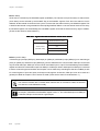
1
MICROCOMPUTER
MN102L00
MN102L59D/59C/F59D
LSI User’s Manual
Pub.No.22259-010E
PanaXSeries is a trademark of Matsushita Electric Industrial Co., Ltd.
The other corporation names, logotypes and product names written in this manual are trademarks or registered
trademarks of their corresponding corporations.
The MN102LF59D is manufactured and sold under the License Agreement with BULL CP8 Inc., and the use of
the MN102LF59D into the IC card is not allowed.
Request for your special attention and precautions in using the technical information and semiconductors described in this manual.
(1)
The approval of the Japanese Government is required for the export of any products and
technologies listed in this manual which are subjected to the provisions of the Foreign
Exchange and Foreign Trade Law.
(2)
The contents of this manual are subject to change without notice to improve design, function, or performance.
(3)
Matsushita Electronics assumes no responsibility or liability for damages or for infringements of patents or other rights arising from use of the information in this manual.
(4)
The contents of this manual may not be copied or reproduced without permission in writing from Matsushita Electronics.
(5)
This manual describes standard specifications. Obtain the latest product standard specifications before you design, purchase, or use.
For inquiries regarding this manual or any Matsushita semiconductor, please contact one of the sales offices listed
at the end of this manual or the sales department of Matsushita Electronics Corporation.
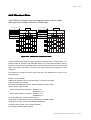
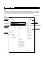
About This Man
ual
Manual
This manual is intended for assembly-language programming
engineers. It describes the internal configuration and hardware
functions of the MN102L59x series microcontrollers.
Text Con
ventions
Conventions
This manual contains titles, sub-titles, special notes and
warnings. Supplementary comments appear in the sidebar.
Key Information
This note describes key points of an operation.
Warning
Please read and follow these instructions to prevent damage
or reduced performance.
Finding Desired Inf
ormation
Information
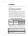
This manual provides four methods for finding desired information quickly and
easily.
(1) An index for the front of the manual for finding each section.
(2) A table of contents at the front of the manual for finding desired titles.
(3) Lists of figures and tables at the front of the manual for finding illustrations
and charts by names.
(4) A chapter name is located at the upper corner of each page.
Related Man
uals
Manuals
■ MN10200 Series Linear Addressing Version LSI User Manual
(Describes the MN10200 series specifications)
■ MN10200 Series Linear Addressing Version Instruction Manual
(Describes the instruction set)
■ MN10200 Series Linear Addressing Version C Compiler User Manual Usage
Guide (Describes the installation, commands, and options for the C complier)
■ MN10200 Series Linear Addressing Version C Compiler User Manual Language Description (Describes the syntax for the C complier)
■ MN10200 Series Linear Addressing Version C Compiler User Manual Library Reference (Describes the standard libraries for the C complier)
■ MN10200 Series Linear Addressing Version Cross Assembler User Manual
Language Description (Describes the assembler syntax and notation)
■ MN10200 Series Linear Addressing Version C Source Code Debugger User
Manual (Describes the use of the C source code debugger)
■ MN10200 Series Linear Addressing Version PanaXSeries Installation
Manual (Describes the installation of the C complier, cross-assembler, and C
source code debugger and the procedures for using the in-circuit emulator)
Questions and Comments
Please send your questions, comments and suggestions to your local semiconductor design center. See the last page of this manual for a list of addresses
and telephone numbers.
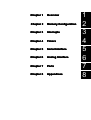
Chapter 1
Overview
Chapter 2
Memory Configuration
Chapter 3
Interrupts
Chapter 4
Timers
Chapter 5
Serial Interface
Chapter 6
Analog Interface
Chapter 7
Ports
Chapter 8
Appendices
1
2
3
4
5
6
7
8
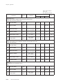
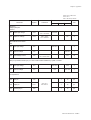
Contents
Chapter 1
1-1
Overview
Overview ...................................................................................................... I-2
1-1-1
Introduction ........................................................................... I-2
1-1-2
Features .................................................................................. I-2
1-1-3
Overview ............................................................................... I-5
1-2
Basic Specifications ..................................................................................... I-8
1-3
Block Diagram ........................................................................................... I-10
1-4
Pin Description ........................................................................................... I-12
1-4-1
List of Pin Functions ........................................................... I-13
1-5
Package Dimension .................................................................................... I-18
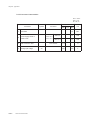
Chapter 2
2-1
Memory Configuration
Memory Configuration ............................................................................... II-2
2-1-1
Overview .............................................................................. II-2
2-1-2
Chapter 3
Interrupts
3-1
Interrupt Groups ........................................................................................ III-2
3-1-1
Overview ............................................................................ III-2
3-2
External Interrupts .................................................................................... III-4
3-2-1
External Pin Interrupts ....................................................... III-4
3-3
3-2-2
NMI Pin Interrupts ............................................................. III-4
3-2-3
External Pin Interrupt Noise Filter .................................... III-5
Interrupt Setup Examples ......................................................................... III-6
3-3-1
External Pin Interrupt Setup ............................................... III-6
3-3-2
Chapter 4
4-1
ii
Contents
Control Registers .................................................................. II-3
Watchdog Timer Interrupt ................................................. III-8
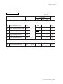
Timers
Timers ........................................................................................................ IV-2
4-1-1
Overview ............................................................................ IV-2
4-1-2
Timer Control Registers ..................................................... IV-9
4-1-3
Timer Block Diagrams ..................................................... IV-11
4-2
4-3
8-bit Timer (Timer 0 to Timer 5) Setup Examples ................................ IV-18
4-2-1
Event Counter Using 8-bit Timer .................................... IV-18
4-2-2
Clock Output Using 8-bit Timer ...................................... IV-20
4-2-3
Interval Timer Using 8-bit Timer .................................... IV-23
8 and 16-bit Timers (Timer 6 to Timer 10) Setup Examples ................ IV-26
4-3-1
Event Counter Using 8 and 16-bit Timers ....................... IV-26
4-3-2
PWM Output Using 8 and 16-bit Timers ........................ IV-28
4-3-3
One-phase Capture Input Using 8 and 16-bit Timers ...... IV-31
4-3-4
External Count Direction Control
Using 8 and 16-bit Timers ................................................ IV-33
4-3-5
Simplified Six-phase PWM Output
by 8-bit Timer (Timer 10) ................................................ IV-35
4-4
4-5
Chapter 5
5-1
Six-phase PWM for Motor Control (Timer 11) ..................................... IV-38
4-4-1
PWM ................................................................................. IV-38
4-4-2
Waveform Mode ............................................................... IV-39
4-4-3
The Polarity of Output Waveform ................................... IV-40
4-4-4
Double Buffer ................................................................... IV-41
4-4-5
Dead Time ........................................................................ IV-43
4-4-6
Fixed Output Setup ........................................................... IV-44
Buzzer Output ......................................................................................... IV-46
4-5-1
Buzzer Output Setup and Operation ................................ IV-46
Serial Interface
Overview ..................................................................................................... V-2
5-1-1
Functions .............................................................................. V-2
5-1-2
Block Diagram ..................................................................... V-3
5-2
Control Registers......................................................................................... V-5
5-2-1
Registers ............................................................................... V-5
5-3
Operation ..................................................................................................... V-6
5-3-1
Clock Synchronous Serial Interface .................................... V-6
5-3-2
Setup Example .................................................................... V-23
5-3-3
UART Serial Interface ....................................................... V-26
5-3-4
Setup Example .................................................................... V-39
iii
Contents
Chapter 6
6-1
Analog Interface
Analog Interface Overview ....................................................................... VI-2
6-1-1
Overview ............................................................................ VI-2
6-1-2
6-2
Control Registers ................................................................ VI-7
Setup Examples ......................................................................................... VI-8
6-2-1
One Channel A/D Conversion Using AN6 Pin ................. VI-8
6-2-2
Multiple Channels A/D Conversion
Using AN2 to AN0 Pins .................................................. VI-10
Chapter 7
7-1
Ports
Ports .......................................................................................................... VII-2
7-1-1
Overview ........................................................................... VII-2
7-1-2
7-2
Chapter 8
Contents
Pull-up/Pull-down Control Register ...................................................... VII-20
7-2-1
Overview ......................................................................... VII-20
Appendices
8-1
Electrical Characteristics ........................................................................ VIII-2
8-1-1
Electrical Characteristics ................................................. VIII-2
8-2
Data Appendices ................................................................................... VIII-17
8-2-1
Special Function Registers ............................................. VIII-17
8-3
iv
Control Registers ............................................................. VII-10
8-2-2
Control Register Address Map ....................................... VIII-96
8-2-3
List of Pin Functions ...................................................... VIII-98
MN10200 Series Linear Addressing Version Instructions ................ VIII-100
8-4
Flash EEPROM Version ..................................................................... VIII-110
8-4-1
Overview ...................................................................... VIII-110
8-4-2
Flash EEPROM Programming ..................................... VIII-111
8-4-3
PROM Programming Mode ......................................... VIII-111
8-4-4
Onboard Serial Programming Mode ............................ VIII-112
8-4-5
Hardware Used in Serial Programming Mode ............... VIII-112
8-4-6
Connecting at Onboard Serial Programming Mode ... VIII-114
8-4-7
System Configuration
at Onboard Serial Programming .................................. VIII-115
8-4-8
Onboard Serial Programming Mode Setup .................. VIII-117
8-4-9
Branch to the User Program ......................................... VIII-119
8-4-10
Serial Interface
Only for Onboard Serial Programming ....................... VIII-120
8-4-11
PROM Writer / Onboard Serial / Programming .......... VIII-121
v
Contents
List of
Figures
Chapter 1 Overview
Figure 1-1-1
Figure 1-1-2
Figure 1-1-3
Figure 1-3-1
Figure 1-4-1
Figure 1-4-2
Figure 1-4-3
Figure 1-5-1
Memory Mode ...................................................................................................... I-5
Interrupt Controller Configuration ....................................................................... I-7
Interrupt Serving Sequence .................................................................................. I-7
Block Diagram .................................................................................................... I-10
Pin Configuration ................................................................................................ I-12
OSCI and OSCO Connection Example .............................................................. I-17
Reset Connection Example ................................................................................. I-17
64-pin LQFP ........................................................................................................ I-18
Chapter 2 Memory Configuration
Figure 2-1-1
Address Space ...................................................................................................... II-2
Chapter 3 Interrupts
Figure 3-3-1
Figure 3-3-2
External Pin Interrupt Timing ........................................................................... III-7
Watchdog Timer Interrupt Timing ................................................................... III-9
Chapter 4 Timers
Figure 4-1-1
Figure 4-1-2
Figure 4-1-3
Figure 4-1-4
Figure 4-1-5
Figure 4-1-6
Figure 4-1-7
Figure 4-1-8
Figure 4-1-9
Figure 4-1-10
Figure 4-1-11
Figure 4-1-12
Figure 4-1-13
Figure 4-1-14
Figure 4-1-15
Figure 4-1-16
Figure 4-1-17
Figure 4-1-18
Figure 4-1-19
Figure 4-1-20
Figure 4-2-1
vi
Contents
Event Counter Timing (Timer 0 to Timer 2) .................................................... IV-5
Timer Output, Interval Timer Timing (Timer 0 to Timer 5) ........................... IV-5
PWM Output Timing (Timer 6 to Timer 9) ..................................................... IV-5
PWM Output Timing (Compensated at Data Write) (Timer 6 to Timer 9) .... IV-6
One-Phase Capture Input Timing (Timer 6 to Timer 9) .................................. IV-6
External Count Direction Control Timing (Timer 6 to Timer 9) .................... IV-6
PWM Output Timing (Timer 10) ...................................................................... IV-7
System Configuration ........................................................................................ IV-8
Timer 0 Block Diagram .................................................................................. IV-11
Timer 1 Block Diagram .................................................................................. IV-11
Timer 2 Block Diagram .................................................................................. IV-12
Timer 3 Block Diagram .................................................................................. IV-12
Timer 4 Block Diagram .................................................................................. IV-13
Timer 5 Block Diagram .................................................................................. IV-13
Timer 6 Block Diagram .................................................................................. IV-14
Timer 7 Block Diagram .................................................................................. IV-14
Timer 8 Block Diagram .................................................................................. IV-15
Timer 9 Block Diagram .................................................................................. IV-15
Timer 10 Block Diagram ................................................................................ IV-16
Timer 11 Block Diagram ................................................................................ IV-17
Event Counter Timing ..................................................................................... IV-19
Figure 4-2-2
Figure 4-2-3
Figure 4-2-4
Figure 4-2-5
Figure 4-3-1
Figure 4-3-2
Figure 4-3-3
Figure 4-3-4
Figure 4-3-5
Figure 4-3-6
Figure 4-3-7
Figure 4-4-1
Clock Output Configuration (1) ...................................................................... IV-20
Clock Output Timing ...................................................................................... IV-22
Clock Output Configuration (2) ...................................................................... IV-23
Interval Timer Timing ..................................................................................... IV-25
Event Counter Timing ..................................................................................... IV-27
PWM Timing ................................................................................................... IV-30
PWM Timing in Double Buffer Mode ........................................................... IV-30
One-phase Capture Timing ............................................................................. IV-32
External Count Direction Control Timing ...................................................... IV-34
PWM Timing ................................................................................................... IV-37
PWM Double Buffer Mode Timing ................................................................ IV-37
PWM (Timer 11) Waveform Mode ................................................................ IV-39
Chapter 5 Overview
Figure 5-1-1
Figure 5-1-2
Figure 5-3-1
Figure 5-3-2-1
Figure 5-3-2-2
Figure 5-3-3-1
Figure 5-3-3-2
Figure 5-3-4
Figure 5-3-5
Figure 5-3-6
Figure 5-3-7
Figure 5-3-8
Figure 5-3-9
Figure 5-3-10
Figure 5-3-11
Figure 5-3-12
Figure 5-3-13
Figure 5-3-14
Figure 5-3-15
Figure 5-3-16
Figure 5-3-17
Figure 5-3-18
Serial Interface 0 Block Diagram ....................................................................... V-3
Serial Interface 1 Block Diagram ....................................................................... V-4
Data Load Period and the Transfer Buffer Empty Flag Operation .................... V-7
Trasfer Bit Count and First Transfer Bit (Starting with MSB) .......................... V-8
Trasfer Bit Count and First Transfer Bit (Starting with LSB) ........................... V-8
Reception Bit Count and First Transfer Bit (Starting with MSB) ..................... V-8
Reception Bit Count and First Transfer Bit (Starting with LSB) ...................... V-8
Transmission Timing (Falling Edge, Start Condition Enabled) ...................... V-13
Transmission Timing (Falling Edge, Start Condition Disabled) ..................... V-13
Transmission Timing (Rising Edge, Start Condition Enabled) ....................... V-14
Transmission Timing (Rising Edge, Start Condition Disabled) ...................... V-14
Reception Timing (Rising Edge, Start Condition Enabled) ............................. V-15
Reception Timing (Rising Edge, Start Condition Disabled) ........................... V-15
Reception Timing (Rising Edge, Start Condition Enabled) ............................. V-16
Reception Timing (Rising Edge, Start Condition Disabled) ............................ V-16
Transmission/Reception Timing
(Reception: Rising Edge, Transmission : Falling Edge) .................................. V-17
Transmission/Reception Timing
(Reception: Falling Edge, Transmission : Rising Edge) .................................. V-17
UART Serial Interface Transmission/Reception Data Format ........................ V-28
Transmission Timing (Parity Bit is Enabled.) .................................................. V-32
Transmission Timing (Parity Bit is Disabled.) ................................................. V-32
Reception Timing (Parity Bit is Enabled.) ....................................................... V-33
Reception Timing (Parity Bit is Disabled.) ...................................................... V-33
vii
Contents
Chapter 6 Analog Interface
Figure 6-1-1
Figure 6-1-2
Figure 6-1-3
Figure 6-1-4
Figure 6-1-5
Figure 6-1-6
Figure 6-1-7
Figure 6-1-8
Figure 6-2-1
Figure 6-2-2
Figure 6-2-3
Analog Interface Configuration ........................................................................ VI-2
Connection of A/D Conversion Input Signal .................................................... VI-2
A/D Conversion Timing .................................................................................... VI-3
One Channel/Single Conversion Timing .......................................................... VI-4
Multiplu Channels/Single Conversion Timing ................................................. VI-4
One Channel/Continuous Conversion Timing.................................................. VI-5
Multiplu Channels/Continuous Conversion Timing ........................................ VI-5
Analog Interface Block Diagram ...................................................................... VI-6
Multiple Channel A/D Conversion ................................................................... VI-8
One Channel A/D Conversion ........................................................................ VI-10
A/D Conversion Timing
(Single Conversion Each of Channel 2 to Channel 0) ................................... VI-11
Chapter 8 Appendices
Figure 8-1
Figure 8-2
Figure 8-3
Figure 8-4
Figure 8-5
System Clock Timing .................................................................................... VIII-15
Reset Timing .................................................................................................. VIII-15
Interrupt Signal Timing ................................................................................. VIII-16
Serial Interface Signal Timing 1
(At Synchronous Serial Interface Falling Edge Transmission
: Timing during Transfer) ..............................................................................VIII-16
Serial Interface Signal Timing 2
(At Synchronous Serial Interface Rising Edge Reception) .......................... VIII-16
Figure 8-6
Timer Counter Signal Timing ........................................................................ VIII-16
Figure 8-4-1 Flash EEPROM Program Flow ................................................................... VIII-111
Figure 8-4-2 8-bit Serial Interface Block Diagram for Serial Writer .............................. VIII-112
Figure 8-4-3 Pin Configuration During Serial Programming .......................................... VIII-114
Figure 8-4-4 System Configuration for Onboard Serial Writer ...................................... VIII-115
Figure 8-4-5 Target Board-Serial Writer Connection ..................................................... VIII-115
Figure 8-4-6 Setup Timing for Onboard Serial Programming Mode .............................. VIII-117
Figure 8-4-7 Determination Flow of Serial Programming Mode .................................... VIII-118
Figure 8-4-8 Reset Service Routine Flow ........................................................................ VIII-119
Figure 8-4-9 Interrupt Service Routine Flow ................................................................... VIII-119
Figure 8-4-10 Data Transfer Timing .................................................................................. VIII-120
Figure 8-4-11 Programming Flow Chart ............................................................................ VIII-121
viii
Contents
List of
Tables
Chapter 1 Overview
Table 1-2-1
Table 1-2-1
Table 1-3-1
Table 1-4-1
Table 1-4-1
Table 1-4-1
Table 1-4-1
Basic Specification (1/2) ....................................................................................... I-8
Basic Specification (2/2) ....................................................................................... I-9
Basic Functions .................................................................................................... I-11
List of Pin Funactions (1/4) ................................................................................. I-13
List of Pin Funactions (2/4) ................................................................................. I-14
List of Pin Funactions (3/4) ................................................................................. I-15
List of Pin Funactions (4/4) ................................................................................. I-16
Chapter 2 Memory Configuration
Table 2-1-1
Control Registers .................................................................................................. II-3
Chapter 3 Interrupts
Table 3-1-1
List of Interrupt Control Registers ..................................................................... III-2
Chapter 4 Timers
Table 4-1-1
Table 4-1-1
Table 4-1-1
Table 4-1-2
Table 4-1-2
Timer Function (1/3) .......................................................................................... IV-2
Timer Function (2/3) .......................................................................................... IV-3
Timer Function (3/3) .......................................................................................... IV-4
Timer Control Registers (1/2) ............................................................................ IV-9
Timer Control Registers (2/2) .......................................................................... IV-10
Chapter 5 Overview
Table 5-1-1
Table 5-2-1
Table 5-3-1
Table 5-3-2
Table 5-3-3
Table 5-3-4
Table 5-3-5
Table 5-3-6
Table 5-3-7
Table 5-3-8
Table 5-3-9
Table 5-3-10
Table 5-3-11
Table 5-3-12
Table 5-3-13
Serial Interface Functions ..................................................................................... V-2
Serial Interface Control Registers ........................................................................ V-5
Synchronous Serial Interface Activation Factor .................................................. V-6
Input Edge and Output Edge of Transmission/Reception Data .......................... V-9
Synchronous Serial Interface Internal Clock Source ......................................... V-10
Last Bit Data Length of Transfer Data .............................................................. V-12
Other Control Flags ............................................................................................V-12
Setup for Synchronous Serial Interfacae Pins (3 Channels, at Transmission) .. V-18
Setup for Synchronous Serial Interfacae Pins (3 Channels, at Reception) ....... V-19
Setup for Synchronous Serial Interfacae Pins
(3 Channels, at Transmission/Reception) .......................................................... V-20
Setup for Synchronous Serial Interface Pins (2 Channels, at Transmission) .... V-21
Setup for Synchronous Serial Interface Pins (2 Channels, at Reception) ......... V-22
Setup for Synchronous Serial Interface Transmission/Reception ..................... V-23
UART Serial Interface Functions ....................................................................... V-26
UART Serial Interface Transmission/Reception Data ...................................... V-28
ix
Contents
Table 5-3-14
Table 5-3-15
Table 5-3-16
Table 5-3-17
Table 5-3-18
Table 5-3-19
Table 5-3-20
Table 5-3-21
Table 5-3-22
Table 5-3-23
Table 5-3-24
Table 5-3-25
Table 5-3-26
UART Serial Interface Frame Mode ................................................................. V-28
Parity Bit of UART Serial Interface ................................................................. V-29
Reception Error Source of UART Serial Interface ........................................... V-29
Other Control Flags ........................................................................................... V-30
Bit Rate Setting at Start-stop Transmission ...................................................... V-35
Bit Rate Setting at Start-stop Transmission ...................................................... V-35
Bit Rate Setting at Start-stop Transmission ...................................................... V-35
Bit Rate Setting at Start-stop Transmission ...................................................... V-35
UART Serial Interface Pins Setup
(1 Channel and 2 Channels, ar Transmission) .................................................. V-36
UART Serial Interface Pins Setup (2 Channels, at Reception) ........................ V-37
UART Serial Interface Pins Setup (1 Channel, at Reception) ......................... V-38
UART Interface Transmission Setup ................................................................ V-39
UART Interface Reception Setup ..................................................................... V-42
Chapter 6 Analog Interface
Table 6-1-1
Table 6-1-2
A/D Converter Functions ................................................................................... VI-3
List of A/D Conversion Control Registers ......................................................... VI-7
Chapter 7 Ports
Table 7-1-1
Table 7-1-1
Table 7-1-1
Table 7-1-1
Table 7-1-1
Table 7-1-1
Table 7-1-1
Table 7-1-2
Table 7-2-1
Port Function (1 of 7) ........................................................................................ VII-3
Port Function (2 of 7) ........................................................................................ VII-4
Port Function (3 of 7) ........................................................................................ VII-5
Port Function (4 of 7) ........................................................................................ VII-6
Port Function (5 of 7) ........................................................................................ VII-7
Port Function (6 of 7) ........................................................................................ VII-8
Port Function (7 of 7) ........................................................................................ VII-9
List of Port Control Registers .......................................................................... VII-10
Pull-up/Pull-down Control Register ................................................................ VII-20
Chapter 8 Appendices
Table 8-4-1
Table 8-4-2
x
Contents
Flash EEPROM Memory Space ................................................................... VIII-113
Clock Frequency ........................................................................................... VIII-116
Chapter 1
Overview
1
2
Chapter 1 Overview
1-1 Over
vie
w
Overvie
view
1-1-1 Intr
oduction
Introduction
The MN10200 series linear addressing version designs the new architecture for
C-language programming based on a detailed analysis for embedded applications. This improves the system architecture in speed and function to meet the
requirements in user systems including miniaturization and low power consumption.
The 16-bit MN102L (F) 59x series has three-phase inverter control function, which
realizes high-efficiency real-time control in motor control.
This series adapts a load/store architecture method for computing within registers and a harvard architecture method for separating instructions bus and operand bus. Using one byte/one machine cycle basic instructions minimizes code
size and improves compiler efficiency.
[Model Explanation]
MN102 L
F 59
D
ROM/RAM sizes
D: 64 k/2 k
C: 48 k/2 k
Model number
Internal ROM
F: Flash
None: Mask ROM
Core version
16-bit 10200 series
1-1-2 Features
This series contains a flexible and optimized hardware architecture as well as a
simple and efficient instruction set. It obtains economical efficiency and high
speed. This section describes the features of this series CPU.
1. Linear Addressing for Large Systems
The MN10200 series contains up to 16 Mbytes of linear address space. The CPU
provides an effective development environment without detecting borders between address spaces. The hardware architecture is also optimized for large
systems. The memory is not divided into instruction space and data space so
that operations can share instructions.
I-2
Overview
Chapter 1 Overview
2. Single-byte Basic Instruction Length
The MN10200 series has replaced general registers with eight internal
CPU registers divided four address registers (A0 to A3) and four data
registers (D0 to D3). The register specification fields are four bits or
less, and the code sizes of the frequently used basic instructions including register- to-register operations and load/store operations are
one byte.
Conventional register assignment
7
15
Register specification field
7
0
Register specification field
New register assignment
3. High-speed Pipeline Processing
The MN10200 series executes instructions in a 3-stage pipeline: fetch,
decode and execute. This allows the MN10200 series to execute instructions of single byte in one machine cycle.
0
1 cycle
Instruction 1
Fetch
Decode
Instruction 2
Address
calculation
Execute
Fetch
Decode
Address
calculation
Execute
4. Simple Instruction Set
The MN10200 series uses an instruction set of 36 instructions, designed specially for the programming model for embedded applications. To compress the
code size, instructions have a variable length of one byte to five bytes. The most
frequently used instructions in C-language compiler are single byte.
5. High-speed Interrupt Response
The MN10200 series can respond quickly to interrupt handling even
during the execution of the instruction with long execution cycles by
suspending it. After an interrupt occurs, the program moves to the interrupt handler within 11 cycles or less. The MN10200 series enhances
real-time control performance using the interrupt handler which adjusts
interrupt handling speed depending on user requirements.
Mainprogram
Instruction 1
Interrupt
processing
program
Instruction 2
Interrupt
request
Instruction 3
Instruction 4
Overview
I-3
Chapter 1 Overview
6. Flexible Interrupt Control Structure
The interrupt controller is divided into eight groups (Group 0 is reserved for NMI.)
and supports a maximum of four vectors for each group in total of 24 vectors.
Each group can be set to one of seven priority levels. This provides the software
design flexibility and accurate control. The CPU is compatible with software from
previous Panasonic peripheral modules.
7. C-Language Development Environment
The MN10200 series contains highly efficient C compiler and simple hardware
optimized for C-language programming. With this advantage, this series improves
development environment for C-language embedded applications without expanding the program size. The PanaXSeries development tools support the MN10200
series devices.
8. Outstanding Power Savings
The MN10200 series contains separate buses which distribute and reduce load
capacitance. This greatly reduces overall power consumption compared to our
conventional models. The MN10200 series also supports two modes of HALT
and STOP for power savings.
I-4
Overview
Chapter 1 Overview
1-1-3 Over
vie
w
Overvie
view
This section describes the basic configuration and function of this
series.
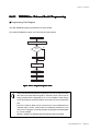
n Address Space
The memory contains up to 16-Mbyte linear address space. The instruction space
and data space are not separated so that internal RAM and special function
registers for internal peripheral functions are allocated into the first 64 KB in memory
as the basic configuration.
x'000000'
This is a general example of the
memory expansion mode.
External memory
x'008000'
Internal RAM
Both the start address and the
end address of internal RAM are
changed within x”008000” to
x”00FBFF” depending on models.
Max
31 KB
x'00FC00'
I/O control register
1 KB
x'010000'
External memory
Program start address
x'080000'
16 MB
x'080000'
Interrupt handler
start address
x'080008'
Max
496 KB
Internal ROM
x'0FC000'
The start address of internal ROM
is fixed at x”080000” while the end
address of internal ROM is
changed depending on sizes of internal ROM. (The end address in
this example is 496 KB.)
External memory
x'FFFFFF'
Figure 1-1-1 Ad
dress Space
Address
Tab
le 1-1-1 Memor
y Modes
able
Memory
Mode
Address bit width
Internal ROM capacity
single chip mode
Up to 24 bits
16 KB or more
External memory area can not be
used in this series. Please refer
to Chapter 2.
Overview
I-5
Chapter 1 Overview
n Internal Registers, Memory and Special Function Registers
Program Counter
23
0
PC
Address Registers
23
The program counter specifies the address (24 bits) of the program
during the execution.
0
The address registers specify the data location on the memory. A3 is
assigned as the stack pointer.
A0
A1
A2
A3
Data Registers
23
0
The data registers perform all arithmetic and logic operations. When the
byte (8-bit) data or the word (16-bit) data is transferred to memory or
another register, the instruction adds a zero or a sign extension.
D0
D1
D2
D3
Multiplication/Division Register
15
0
MDR
Processor Status Word
15
0
PSW
The multiplication/division register stores the upper 16 bits of the 32-bit
product of the multiplication operations. In division operations, this register stores the upper 16 bits of the 32-bit dividend before the execution
and the 16-bit remainder of the quotient after the execution.
The processor status word indicates the CPU status. This register stores
the operation result flags and interrupt mask levels.
Memory, Special Registers, I/O Ports
ROM
Memory (ROM and RAM), special registers for controlling peripheral
functions and I/O ports are assigned to the same address space.
RAM
CPUM, MEMCTR, IAGR
Internal Control Registers
SYSCTL
System Control Registers
GnICR, EXTMD, NFCTR, ...
Interrupt Control Registers
SCnMD0, SCnMD1, SCnMD2, ...
ANCTR, ANBUF
TMnMD, TMnBC, TMnBR, ...
PnMD, PnDIR, PnOUT, ...
I-6
Overview
Serial Interface
A/D Converter
Timers/Counters
I/O Ports
Chapter 1 Overview
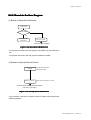
n Interrupt Controller
The interrupt controller (group 0 to group 7) allocated to the outside of the CPU
controls all nonmaskable interrupts and maskable interrupts except reset. Each
group contains up to four interrupt vectors and specifies any of seven priority
levels.
CPU Core
Maskable Interrupt
Receive
Non-maskable Interrupt
Receive
Reset
Receive
Reset
Interrupt Controller
Interrupt Enable
Non-maskable Interrupts
Non-maskable Interrupt Controller
Group 0 (G0ICR)
Interrupt Mask
6
5
4
3
2
1
3
0
Watchdog Timers
Execution of Undefined Instructions
External Pin NMI
4
Maskable Interrupt Controller
Group 1 (G1ICR)
Maskable Interrupts
21 Vectors
2
Maskable Interrupt Controller
Group 7 (G7ICR)
External Pin Interrupts
Peripheral Interrupts, etc.
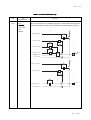
Figure 1-1-2 Interrupt Contr
oller Configuration
Controller
The CPU checks the processor status word to determine whether an interrupt
request is accepted or not. When an interrupt is accepted, automatic servicing by
hardware starts and the program counter and PSW are pushed to the stack.
Next, the program moves to the interrupt. After specifying the interrupt vector, it
branches to the entry address of the interrupt service for that interrupt.
Interrupt preprocessing
Push registers, branch to entry address, etc.
Main Program
x'080008'
Interrupt handling routine
Reset interrupt vectors
at the beginning
Hardware processing
Push PC, PSW
JMP, etc.
Interrupt
Max. of 4 machine cycles
7 machine cycles
Figure 1-1-3 Interrupt Ser
vicing Sequence
Servicing
Overview
I-7
Chapter 1 Overview
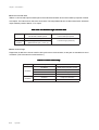
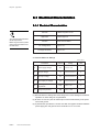
1-2 Basic Specifications
This section describes the basic specification of this series. Please
refer to Product Standards for details.
Tab
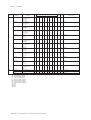
le 1-2-1 Basic Specifications (1/2)
able
CPU Structure
Load/store architecture
Eight registers: Four 24-bit data registers
Four 24-bit address registers
: 24-bit program counter
Others
16-bit processor status word
16-bit multiplication/division register
Instruction
36 instructions
6 addressing modes
One-byte primitive instruction length
Code assignment: 1 to 2 bytes (Basic) + 0 to 3 bytes (Extension)
Basic Performance
10 MHz internal operating frequency with a 5-MHz oscillator and internal 4x-speed
Clock cycles: For instruction execution, minimum 1 cycle (100 ns)
For register-to-register operations, minimum 1 cycle
For load/store operations, minimum 1 cycle
For conditional branching operations, 1 to 3 cycles
Pipeline
3 stages: Instruction fetch, decode, execute
Address Space
16-MB linear address space
Low-power Mode
STOP mode, HALT mode
Frequency Circuit
Outside: Up to 5 MHz (Inside 20 MHz : Internal 4x-speed)
Interrupt
24 vectors
3 non-maskable interrupts
21 maskable interrupts (7 interrupt priority level settings)
7 external interrupts
6 external interrupts (individual IRQ, edge specification)
1 external non-maskable interrupt
17 internal interrupts
12 timer interrupts, 2 serial interrupts, 1 A/D interrupt,
1 watchdog timer interrupt, 1 undefined instruction interrupt
I-8
Basic Specifications
Chapter 1 Overview
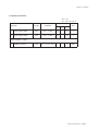
Tab
le 1-2-1 Basic Specifications (2/2)
able
Timer/Counter
Nine 8-bit timers
Reload timer
Cascading function
Timer output (duty of 1:1)
Internal clock source or external clock source
Serial interface clock generation
Start timing generation for A/D converter
Output 2 channels simplified PWM
Output 1 channel simplified 6-phase PWM
Three 16-bit timers
Compare registers
Internal clock source or external clock source
Timer output (duty of 1:1)
PWM
1 channel high-efficiency inverter control (output 6-phase PWM)
17-bit watchdog timer
Serial Interface
2 half duplex UART/synchronous (shared) serial interfaces
Analog Interface
A/D converter
Twelve 10-bit inputs (4 channels are shared.)
Auto scanning (0 to 7 channel settings)
I/O Port
52 I/O ports (All shared pins)
Package
64-pin LQFP
pitch: 0.8 mm
dimension: 14-mm-square
Basic Specifications
I-9
Chapter 1 Overview
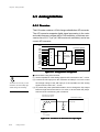
1-3 Bloc
k Dia
gram
Block
Diagram
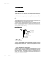
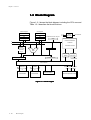
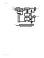
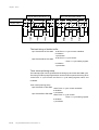
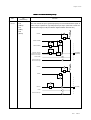
Figure 1-3-1 shows the block diagram including the CPU core and
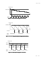
Table 1-3-1 describes the block functions.
Address Registers
Data Registers
A0
D0
A1
D1
A2
D2
Multiplication/Division Register
A3
D3
MDR
T1
T2
4x-speed
Clock
Generator
Clock Source
Instruction Execution
Controller
A
B
Instruction Decoder
Program
Counter
PSW
Increment
ALU
Instruction
Queue
Interrupt
Controller
Operand Address
Program Address
Interrupt Bus
Bus Controller
ROM Bus
RAM Bus
Internal ROM
Internal RAM
Peripheral Extension Bus
External Interface
Figure 1-3-1 Bloc
k Dia
gram
Block
Diagram
I - 10
Block Diagram
Internal Peripheral Function
Chapter 1 Overview
Tab
le 1-3-1 Bloc
k Functions
able
Block
Block
Functions
Clock Generator
The clock generator contains the clock oscillation circuit connected to an external
crystal and supplies the clock to all CPU blocks. (It has a built-in 4x-speed circuit.)
Program Counter
The program counter generates addresses for instruction queues. Normally, it
gets increments based on the sequencer indication, but for branch instructions
and interrupt acceptance, it sets the branch address or ALU operation results.
Instruction Queue
The instruction queue saves up to 4 bytes of prefetched instructions.
Instruction Decoder
The instruction decoder decodes the instruction queue content, generates control signals needed for the instruction execution, and executes the instruction by
controlling each block in the CPU.
Instruction Execution
Controller
The instruction execution controller controls the operations of each CPU function
based on results from the instruction decoder and interrupt requests.
ALU
The ALU calculates the operand addresses for arithmetic operations, logic operations, shift operations, register relative indirect, indexed addressing and register
indirect addressing mode.
Internal ROM, Internal RAM
Internal ROM and internal RAM are allocated as the execution program, data and
stack areas.
Address Registers
(An)
The address registers (An) store the addresses of memory accessed during data
transfer. They also store the base addresses in the register relative indirect,
indexed addressing and register indirect addressing mode.
Operation Registers
(Dn, MDR)
The data registers (Dn) store the operation results and transfer the data to memory.
They also store the offset addresses in indexed addressing and register indirect
addressing mode.
The multiplication/division register (MDR) stores the data for multiplication/division operations.
PSW
The processor status word (PSW) stores the flags that indicate the status of the
CPU interrupt controller and operation results.
Interrupt Controller
The interrupt controller detects the interrupt requests from the peripheral functions, and requests the CPU to move to the interrupt handling.
Bus Controller
The bus controller controls the connection between the CPU internal bus and the
CPU external bus. It also contains the bus arbitration function.
Internal Peripheral Function
This series contains the peripheral functions including timers, serial interface,
A/D converter and so on.
Block Diagram
I - 11
Chapter 1 Overview
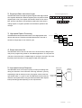
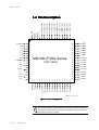
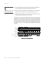
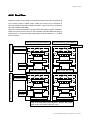
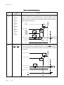
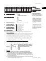
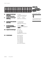
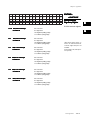
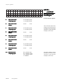
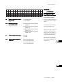
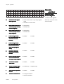
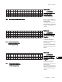
*
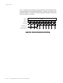
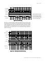
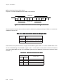
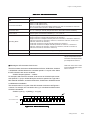
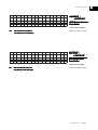
VDD
P65,TPWM5,SBO1
P64,TPWM4,SBI1
P63,TPWM3,SBT1
P62,TPWM2,SBO0
P61,TPWM1,SBI0
P60,TPWM0,SBT0
P45,PWM2,STOP
P44,PWM2,TM7IO
P43,PWM1,TM6IO
P42,PWM1,TM2IO
P41,PWM0,TM1IO
P40,PWM0,TM0IO
61
60
59
58
57
56
55
54
53
52
51
50
49
*
63
62
NMI
64
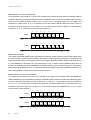
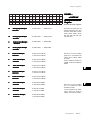
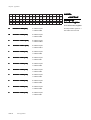
1-4 Pin Description
P70,BUZZ
1
48
P25,IRQ5
P71
2
47
P24,IRQ4
P72
3
46
P23,IRQ3
P73
4
45
P22,IRQ2
P74
5
44
P21,IRQ1
P75
6
43
P20,IRQ0
P76
7
42
P16,TM9IO
P77,WDOUT
8
41
P15,TM8IO
VSS
9
40
P14,TM7IO
RST
10
39
P13,TM6IO
VSS
11
38
P12,TM2IO
SYSCLK
12
37
P11,TM1IO
VDD
13
36
P10,TM0IO
OSCI
14
35
P02,SBO0
OSCO
15
34
P01,SBI0
VDD
16
33
P00,SBT0
MN102L(F)59x Series
17
18
19
20
21
22
23
24
25
26
27
28
29
30
31
32
P50
P51
P52
P53
P54,AN11
P55,AN10
P56,AN9
P57,AN8
P30,AN7
P31,AN6
P32,AN5
P33,AN4
P34,AN3
P35,AN2
P36,AN1
P37,AN0
(TOP VIEW)
*: Use 4.7 kΩ to 10 kΩ.
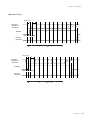
Figure 1-4-1 Pin Configuration
The unused input pins are connected to VDD/VSS, the unused output pins
are opened and the unused I/O pins are connected to V DD/VSS by setting
the direction in ports or opened.
I - 12
Pin Description
Chapter 1 Overview
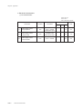
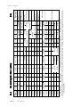
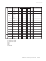
1-4-1 List of Pin Functions
Refer to “8-2-3 List of Pin Functions” for each pin’s input level, and Schmitt and
pull-up resistor availability. TTL in the input level column means that the input is
determined at TTL level. CMOS in the input level column means that the input is
determined at CMOS level. The column with “yes” sign shows Schmitt, while the
column with no mark shows no Schmidt. Pull-up and pull-down resistors are in
the column with “yes”. The column with “programmable” can be set by pull-up and
puill-down control registers (PPUP, PPDW). Please see “Chapter 7 Ports” for details.
Tab
le 1-4-1 List of Pin Functions (1/4)
able
Pin Name
Input/Output Shared Pin
Function
Power
VDD
Description
There are three VDD pins. Connect these three
pins to a power supply of 4.5 V to 5.5 V.
VSS
Power (Ground)
There are two VSS pins. Connect these two pins
to a power supply of 0 V.
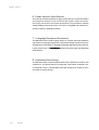
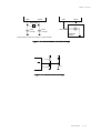
OSCI
Input
High-speed Oscillator
For a self-excited oscillator configuration, connect
OSCO
Output
Input (Max: 5 MHz)
High-speed Oscillator
crystal or ceramic oscillator across these two pins.
They have a built-in feedback resistor between
them. For stability, insert capacitor of 20 pF to 33
Output (Max: 5 MHz )
pF between the OSCI or OSCO pin and VSS pin.
(For the exact capacitance, consult the oscillator
manufacturer.) [
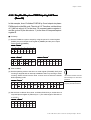
Figure 1-4-2 OSCI and
OSCO Connection Example]
For an external oscillator configuration, connect
the OSCI pin to an oscillator with an amplitude of
maximum 5 MHz at the width between VDD and
VSS. Leave the OSCO open.
Connecting the OSCO pin with the external circuit is not allowed. Select the SYSCLK pin as a
synchronous signal.
RST
Input
Reset Input
This pin resets the chip. With a 5-MHz oscillator, reset starts when the low level is input to this
pin for more than 200 ns. Reset may start even
when the noise is input to this pin for less than
200 ns, so please pay highly attention to noise.
Reset is released when the high level is input to
the pin. The oscillation waits of the high-speed
oscillation pin (OSCI) are performed (approximately 6 ms to 7 ms with a 5-MHz oscillator).
After that, the chip starts executing the instruction from x”080000”. [
Figure 1-4-3 Reset
Connection Example]
Pin Description
I - 13
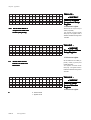
Chapter 1 Overview
Tab
le 1-4-1 List of Pin Functions (2/4)
able
Pin Name
SYSCLK
Input/Output Shared Pin
System Clock Output
Output
Description
Function
This pin provides the system clock. After reset
release, the oscillation waits of OSCI are always
performed and this pin outputs the clock of 10
MHz at a 5-MHz oscillation. Please keep in mind
that this pin holds the high level until the oscillation waits are released after the RST pin becomes
the low level.
P70
I/O
General-purpose Port 7 This pin can be used as a general-purpose input/
output port. [
Output
BUZZ
Buzzer Output
Chapter 7 Ports ]
This pis outputs the square wave that divides 1/
Chapter 4
211 to 1/214 of system clock. [
Timers ]
P76 to P71
I/O
General-purpose Port 7 These pins can be used as general-purpose input/output ports. [
Chapter 7 Ports ]
P77
I/O
General-purpose Port 7 This pin can be used as a general-purpose input/
output port. [
Output
P53 to P50
WDOUT
I/O
Watchdog Timer
Overflow Signal
When the watchdog timer is overflowed, pulse is
output.
When these pins are used as general-purpose
input/output ports, input/output direction control
General-purpose Port 5
is bit-oriented. [
P57 to P54
I/O
Chapter 7 Ports ]
Chapter 7 Ports ]
When these pins are used as general-purpose
General-purpose Port 5
input/output ports, input/output direction control
is bit-oriented.
Input
P37 to P30
I/O
Input
AN11 to
AN8
A/D Converter Input
These are input pins for A/D converter.
[
General-purpose Port 3 When these pins are used as general-purpose
input/output ports, input/output direction control
is bit-oriented.
AN7 to AN0 A/D Converter Input
These are input pins for A/D converter.
[
I - 14
Pin Description
Chapter 6 Analog interface ]
Chapter 6 Analog interface ]
Chapter 1 Overview
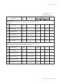
Tab
le 1-4-1 List of Pin Functions (3/4)
able
Pin Name
P00
Input/Output Shared Pin
P01
P02
I/O
Input
SBI0
General-purpose Port 0 These pins can be used as synchronous transfer
Serial Interface 0
clock signals, data input and data input/output for
Data Input
serial interface.
I/O
I/O
P16 to P10
SBT0
General-purpose Port 0 When this pin is used as a general-purpose inSerial Interface 0
put/output port, input/output direction control is
Clock Input/Output
bit-oriented. [
Chapter 7 Ports ]
I/O
I/O
Description
Function
SBO0
I/O
When these are unused, the input pins are fixed
General-purpose Port 0 as high level while the output pins are opened.
Serial Interface 0
[
Chapter 5 Serial Interface ]
Data Input/Output
General-purpose Port 1
When these pins are used as general-purpose
input/output ports, input/output direction control is bit-oriented. [
I/O
TM9IO to
TM6IO
Timer 9 to Timer 6
TM2IO to
Timer 2 to Timer 0
Input/Output
TM0IO
P25 to P20
I/O
Input/Output
General-purpose Port 2
These pins are timer 9 to timer 6 input/output
pins.
These pins are timer 2 to timer 0 input/output
pins.
[
Chapter 4 Timers ]
When these pins are used as general-purpose
input/output ports, input/output direction control
is bit-oriented. [
Input
IRQ5 to
Chapter 7 Ports ]
Chapter 7 Ports ]
External Interrupt
IRQ0
Pin Description
I - 15
Chapter 1 Overview
Tab
le 1-4-1 List of Pin Functions (4/4)
able
Pin Name
P45 to P40
Input/Output Shared Pin
General-purpose Port 4
I/O
Description
Function
When these pins are used as general-purpose
input/output ports, input/output direction control is bit-oriented. [
Output
Output
STOP
PWM2 to
PWM0
Chapter 7 Ports ]
STOP Status Signal
These pins become high level during STOP or
HOLT mode.
Timer 11 Output
These are output pins of timer 11 (6-phase
PWM wave form).
PWM2 to
PWM0
I/O
TM7IO,
TM6IO
TM2IO to
TM0IO
P65 to P60
I/O
Timer 7 and 6 Input/
Output
These are input/output pins of timer 7 and timer
6.
Timer 2 to 0 Input/Out-
These are input/output pins of timer 2 to 0.
put
[
General-purpose Port 6
When these pins are used as general-purpose
Chapter 4 Timers ]
input/output ports, input/output direction control is bit-oriented. [
Chapter 7 Ports ]
Output
I/O
Input
Output
NMI
Input
TPWM5 to
TPWM0
Timer 10 Output
SBT1 to 0
Serial Interface
Clock Input/Output
SBT1 to 0
SBO1 to 0
These are output pins of timer 10 (Simplified 6phase PWM waveform). [
Timers ]
Serial Interface
Data Input/Output
Chapter 4
These pins can be used as synchronous transfer clock signal, data input and data output for
serial interface.
When these are unused, the input pins are fixed
as high level while the output pins are opened.
[
Chapter 5 Serial interface ]
Serial Interface
Data Output
NMI
An NMI interrupt occurs on the falling edge to
low level at negative logic. (When reading the
Port 2, the pin value can be monitored at bit 6.)
I - 16
Pin Description
Chapter 1 Overview
l
OSCI
OSCO
OSCI
Max 5 MHz
OSCO
l
20 pF
to 33 pF
20 pF
to 33 pF
Max 5 MHz
Oscillation
Circuit
(Note)Capacity varies acoording to crystal oscillator.
Figure 1-4-2 OSCI and OSCO Connection Example
Di
10 kΩ to 50 kΩ
RST
+
10 µF to 100µF
SW
Figure 1-4-3 Reset Connection Example
Pin Description
I - 17
Chapter 1 Overview
1-5 P
ac
ka
ge Dimension
Pac
acka
kag
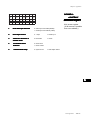
Package Code: LQFP064-P-1414
unit: mm
Body Material: Epoxy Resin, Lead Material: Cu Alloy, Lead Finish Method: Pd Plating
Figure 1-5-1
64-pin LQFP
The package dimension is subject to change. Before using this product, please obtain product specifications from the sales office.
I - 18
Overview
Chapter 2
Memory Configuration
1
2
3
Chapter 2 Memory Configuration
2-1 Memor
y Configuration
Memory
2-1-1 Over
vie
w
Overvie
view
This series operates at the single chip mode.
x'000000'
Access Prohibited Area
(56 KB)
x'00E000'
x'00E800'
x'00FC00'
x'010000'
Internal RAM Area
(2 KB)
Access Prohibited Area
(5 KB)
Special Registers Area
(1 KB)
Access Prohibited Area
(448 KB)
x'080000'
Internal ROM Area
(48 KB or 64 KB)
x'08C000'
or x'090000'
Access Prohibited Area
x'FFFFFF'
Figure 2-1-1 Ad
dress Space
Address
II-2
Memory Configuration
Chapter 2 Memory Configuration
2-1-2 Contr
ol Register
s
Control
Registers
Memory is controlled by the memory control register (MEMCTR) and the system control
register (SYSCTL).
Tab
le 2-1-1 Contr
ol Register
s
able
Control
Registers
Register Symbol
Address
R/W
Register Name
MEMCTR
X'00FC02'
R/W
Memory control register
SYSCTL
X'00FC32'
R/W
System control register
MEMCTR has to be set up to be agreeable to the system configuration in the initialization program.
MEMCTR register of this series sets up x’04n0’ (n=0 to 3: These are wait
number of the special register. 1 is usual.) in the initialization program.
Memory Configuration
II-3
Chapter 3
Interrupts
2
3
4
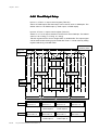
Chapter 3 Interrupts
3-1 Interrupt Gr
oups
Groups
3-1-1 Over
vie
w
Overvie
view
The interrupt controller contains eight groups. Each group has some
interrupt vectors . When an interrupt occurs, the CPU receives an
interrupt request. [
MN10200 Series LSI User’s Manual Linear
Addressing Version]
Tab
le 3-1-1 List of Interrupt Contr
ol Register
s
able
Control
Registers
Interrupt Vector
(Number is IDTn bit position)
Interrupt Group
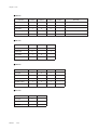
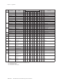
Group 0
2 Undefined Instruction Interrupt
1 Watchdog Timer Interrupt
0 NMI Interrupt
Non-maskable Interrupt Control Register 0
G0ICR: x'00FC40'
Group 1
3
2
1
0
Timer/Counter 0 Underflow
External Interrupt IRQ2
External Interrupt IRQ1
External Interrupt IRQ0
Maskable Interrupt Control Register 1
G1ICR: x'00FC42'
Group 2
3
2
1
0
A/D Conversion End
External Interrupt IRQ5
External Interrupt IRQ4
External Interrupt IRQ3
Maskable Interrupt Control Register 2
G2ICR: x'00FC44'
Group 3
3
2
1
0
Reserved
Serial Ch0 Transmission End
Timer/Counter 2 Underflow
Timer/Counter 1 Underflow
Maskable Interrupt Control Register 3
G3ICR: x'00FC46'
Group 4
3
2
1
0
Reserved
Serial Ch1 Transmission End
Timer/Counter 8 Underflow
Timer/Counter 3 Underflow
Maskable Interrupt Control Register 4
G4ICR: x'00FC48'
Group 5
3
2
1
0
Reserved
Timer/Counter 9 Underflow
Timer/Counter 5 Underflow
Timer/Counter 4 Underflow
Maskable Interrupt Control Register 5
G5ICR: x'00FC4A'
Group 6
3
2
1
0
Reserved
Reserved
Timer/Counter 6 Underflow
Timer/Counter 10 Overflow
Maskable Interrupt Control Register 6
G6ICR: x'00FC4C'
Group 7
3 Unavailable (Set the corresponding
enable flag always to 0.)
2 Unavailable (Set the corresponding
enable flag always to 0.)
1 Timer/Counter 7 Underflow
0 Timer/Counter 11 Underflow/Overflow
Reserved: A corresponding flag does not actually exist.
III-2
Control Register
Interrupt Groups
Maskable Interrupt Control Register 7
G7ICR: x'00FC4E'
Chapter 3 Interrupts
The control registers are assigned to each corresponding interrupt group except
Group 0 and control the assigned interrupt vectors. For example, in the MN102L(F)
59x, when timer 0 becomes underflow, the interrupt request flag (IRF3=TM0IR)
of the maskable interrupt control register 1 (G1ICR) becomes 1. At this point, an
interrupt request is output to the CPU core if the corresponding interrupt enable
flag (IEN3=TM0IE) is 1. Comparing the interrupt mask level (IM2 to 0 ) of the
processor status word (PSW) with the group interrupt level (ILVn=G1LV[2:0]) of
the G1ICR register and the interrupt enable flag (IE) of PSW determine whether
the CPU core receives the interrupt or not.
Change of G1ICR interrupt level
(ILVn) and interrupt enable flag
(IENn) should be executed when
PSW enable flag (IE) is 0.
G1ICR: x’00FC42’
15
14
13
12
G1
LV2
G1
LV1
G1
LV0
↓
11
9
10
8
7
6
5
4
3
2
1
0
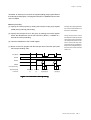
TM0 IRQ2 IRQ1 IRQ0 TM0 IRQ2 IRQ1 IRQ0 TM0 IRQ2 IRQ1 IRQ0
IE
IE
IR
ID
IE
IR
IE
IR
IR
ID
ID
ID
↓
↓
Group interrupt level Interrupt enable flag Interrupt demand flag
IENn
IRFn
ILVn
Occurrence of
Setup of interrupt level Setup of interrupt
permission
interrupt factor
↓
Interrupt detective
flag
IDTn
Detection of interrupt
demand
Please refer to “2-5 Interrupt Controller” in the MN10200 Series LSI User’s Manual
Linear Addressing Version for detail operations, and the MN10200 Series Instruction Manual Linear Addressing Version for interrupt handling flow and handler
programming.
Set the interrupt enable flags IEN [3:2] (bits [11:10]) of the G7ICR
always to 0.
Interrupt Groups
III-3
Chapter 3 Interrupts
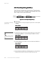
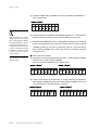
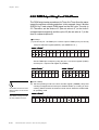
3-2 External Interrupts
3-2-1 External Pin Interrupts
Group 1 to Group 5 control external pin interrupts.
The EXTMD register sets the interrupt conditions.
The EXTMD register sets the interrupt levels and timing of external interrupts,
and specifies each pins’ level or edge.
EXTMD: x’00FC50’
15
14
13
12
11
10
9
8
7
6
5
4
3
2
1
0
IRQ5 IRQ5 IRQ4 IRQ4 IRQ3 IRQ3 IRQ2 IRQ2 IRQ1 IRQ1 IRQ0 IRQ0
TG1 TG0 TG1 TG0 TG1 TG0 TG1 TG0 TG1 TG0 TG1 TG0
↑
EIRQ5
↑
EIRQ4
↑
EIRQ3
↑
EIRQ2
↑
EIRQ1
↑
EIRQ0
00: An interrupt occurs at low level.
01: An interrupt occurs at high level.
10: An interrupt occurs at negative edge.
11: An interrupt occurs at positive edge.
3-2-2 NMI Pin Interrupts
This series supports an NMI interrupt. The NMI interrupt occurs on the negative
edge of NMI pin.
III-4
External Interrupts
Chapter 3 Interrupts
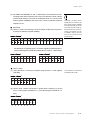
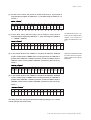
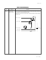
3-2-3 External Pin Interrupt Noise Filter
External interrupt pins IRQ0 to IRQ3 and NMI have the built-in noise
clearing circuit.
NFCTR: x’00FC52’
15
14
13
12
11
10
9
8
7
6
5
4
3
2
1
0
IRQ3 IRQ3 IRQ2 IRQ2 IRQ1 IRQ1 IRQ0 IRQ0 NMI NMI
FSE FEN FSE FEN FSE FEN FSE FEN SEL1 SEL0
↑
IRQ3
↑
IRQ2
↑
IRQ1
↑
IRQ0
↑
NMI
IRQnFEN 0: Noise filter is off.
1: Noise filter is on.
IRQnFSE 0: Sampling at 22 machine cycle
1: Sampling at 27 machine cycle
00: Sampling at 1 machine cycle
01: Sampling at 22 machine cycle
10: Sampling at 27 machine cycle
11: unavailable
The waveform that is input from the interrupt pins is sampled. As for IRQ0 to
IRQ3, when low level interrupt or negative edge interrupt is set, if low level is input
for more than 4 sampling periods, an interrupt signal is input inside of CPU.
When high level interrupt or positive edge interrupt is set, if high level is input for
more than 4 sampling periods, an interrupt signal is input inside of CPU.
The noise filter is unavailable at STOP mode and HALT mode.
External Interrupts
III-5
Chapter 3 Interrupts
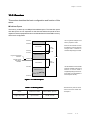
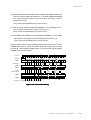
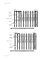
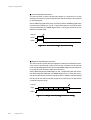
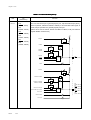
3-3 Interrupt Setup Examples
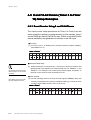
3-3-1 External Pin Interrupt Setup
An interrupt occurs on the negative (falling) edge from the external
interrupt pin IRQ0 (P20).
The external interrupt edge specification register (EXTMD) is set to the interrupt
request generation at low level after reset release, and the IRQ0IR bit of the
maskable interrupt control register 1 (G1ICR) becomes 0.
n Interrupt Enable Setup
(1) Set the interrupt conditions of the interrupt pin IRQ0 (P20). In this case, set
the IRQ0TG of the EXTMD register to 2 (bit string 10:negative edge).
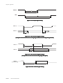
EXTMD: x’00FC50’
15
14
13
12
11
10
9
8
7
6
5
4
3
2
1
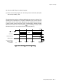
0
IRQ5 IRQ5 IRQ4 IRQ4 IRQ3 IRQ3 IRQ2 IRQ2 IRQ1 IRQ1 IRQ0 IRQ0
TG1 TG0 TG1 TG0 TG1 TG0 TG1 TG0 TG1 TG0 TG1 TG0
-
In this example, the interrupt level
is 4.
-
-
-
0
0
0
0
0
0
0
0
0
0
1
0
(2) Enable interrupts. At this point, clear all prior interrupt requests. To do this,
set G1LV[2:0], IRQ0IR and IRQ0IE of the maskable interrupt control register 1 (G1ICR) to an interrupt level, 0 and 1, respectively.
G1ICR: x’00FC42’
15
-
14
13
12
G1
LV2
G1
LV1
G1
LV0
0
0
1
11
10
9
8
7
6
5
4
3
2
1
0
TM0 IRQ2 IRQ1 IRQ0 TM0 IRQ2 IRQ1 IRQ0 TM0 IRQ2 IRQ1 IRQ0
IE
IE
IR
ID
IE
IR
IE
IR
IR
ID
ID
ID
0
0
0
1
0
0
0
0
0
0
0
0
(3) Enable interrupts by setting the interrupt enable flag (IE) of the processor
status Word (PSW) to 1 and the interrupt mask level (IMn) to 7 (bit string
111).
III-6
Interrupt Setup Examples
Chapter 3 Interrupts
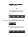
Thereafter, an interrupt occurs when the negative (falling) edge is generated on
the interrupt pin IRQ0 (P20). The program branches to x’080008’ when the interrupt is accepted.
n Interrupt Handling
(4) Specify the interrupt group by reading the interrupt accept group register
(IAGR) during interrupt prehandling.
(5) Specify the interrupt vector in the group by reading the G1ICR register.
Check the IRQ0ID with the bit test instruction (BTST). If IRQ0ID is 1,
execute the interrupt handling.
(6) Clear the IRQ0IR bit of the G1ICR register.
(7) Return to the main program with the interrupt return instruction (RTI) after
the interrupt handling ends.
Normally, the program generates
the interrupt start address and
branches to that address.
During interrupt service routine,
the IM and IE of PSW become the
interrupt level and 0 respectively.
The multiple interrupts are not allowed. It means that other interrupts except the non-maskable interrupt are not accepted during interrupt service routine unless the
PSW is set.
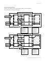
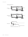
P20 (IRQ0)
EXTMD
Low Level
Negative Edge
IRQ0IE
IRQ0IR
Interrupt Handling
Registers [R/W]
Procedure
EXTMD(W) G1ICR(R)
(1)
(2)
G1ICR(R/W)
(3)(4)(5)(6)(7)
G1ICR(R/W)
(4)(5)(6)(7)
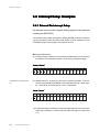
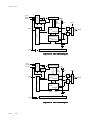
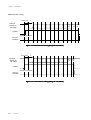
Figure 3-3-1 External Pin Interrupt Timing
Interrupt Setup Examples
III-7
Chapter 3 Interrupts
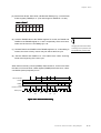
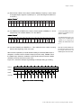
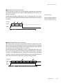
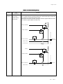
3-3-2 Watc
hdog Timer Interrupt
atchdog
An interrupt occurs by using the watchdog timer.
When the watchdog fanction is used, operation is started by setting the WDRST
flag of the CPU mode control register (CPUM) to enable (‘0’) after reset. The
watchdog timer needs to be cleared during the main program because a nonmaskable interrupt occurs when the watchdog counter overflows.
n Interrupt Enable Setup
When the watchdog timer counts
65536 cycles of SYSCLK (6.5536
ms with a 20-MHz oscillator), a
watchdog interrupt occurs. Watchdog interrupt occurring term can
be extended 8, 16 or 32 times by
the watchdog timer expansion
control register.
(1) Enable interrupts by setting the interrupt enable flag (IE) of the processor
status Word (PSW) to 1 and the interrupt mask level (IMn) to 7 (bit string
111).
(2) Clear the WDRST flag of the CPUM register. This starts the watchdog
timer.
CPUM: x’00FC00’
15
14
13
12
11
10
9
8
7
6
5
0
0
3
2
1
0
OSC STOP HALT OSC1 OSC2
ID
WD WD WD
RST LNG1 LNG0
0
4
-
-
-
-
-
-
-
-
0
0
0
0
0
n Watchdog Timer Clear
Normally, clear the watchdog
timer before an interrupt occurs.
Normally, the program generates
the interrupt start address and
branches to that address.
The IM of PSW becomes the highest level during interrupt handling
and other interrupts are not accepted.
III-8
Interrupt Setup Examples
(3) Set the WDRST flag of the CPUM register to 1 and then immediately clear
to 0. The watchdog timer is cleared to 0 when the WDRST flag is 1.
n Interrupt Handling
The program branches to x’080008’ when an interrupt is generated and accepted.
(4) Specify the interrupt group by reading the interrupt accept group register
(IAGR) during interrupt prehandling.
(5) Verify a watchdog interrupt by reading the nonmaskable interrupt control
register (G0ICR). Check the WDIF with the bit test instruction (BTST). If
WDIF is 1, execute the interrupt service routine.
Chapter 3 Interrupts
(6) Clear the WDIF flag of the G0ICR register.
(7) Return to the main program with the interrupt return instruction (RTI) after
the interrupt handling ends.
The watchdog timer and the oscillation stabilization wait counter are shared. The
watchdog timer operates as the oscillation stabilization wait counter when the
CPU returns from the STOP mode. Because of this, the WDIF flag is cleared to
0 when the CPU moves to the STOP mode. The WDIF flag is cleared to 0 again
after the CPU moves to the normal mode. [
“2-6 Standby Function” in the
MN10200 Series LSI User’s Manual Linear Addressing Version]
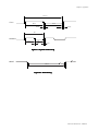
Overflow
RST Pin
Clear
WD Count
WDRST(CPUM)
WDIF(G0ICR)
Interrupt Handling
Registers [R/W]
Procedure
(1)
CPUM(W)
(2)
CPUM(W)
(3)
CPUM(W)
(3)
G0ICR(R/W)
(4)(5)(6)(7)
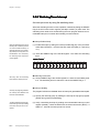
Figure 3-3-2 Watc
hdog Timer Interrupt Timing
atchdog
Interrupt Setup Examples
III-9
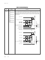
Chapter 4
Timers
3
4
5
Chapter 4 Timers
4-1 Timer
s
Timers
4-1-1 Over
vie
w
Overvie
view
This LSI series contains nine 8-bit timers (timer 0 to timer 5 and
timer 8 to timer 10) and three 16-bit timers (timer 6, timer 7 and
timer11).
Tab
le 4-1-1 Timer Function (1/3)
able
8-bit Timer
Timer
Function
Timer 0
Timer 1
Timer 2
Timer 3
Interrupt Request Destination
Group 1 (G1ICR)
- TM0IR
Group 3 (G2ICR)
- TM1IR
Group 3 (G3ICR)
- TM2IR
Group 4 (G4ICR)
- TM3IR
Interrupt Source
Timer 0 underflow
Timer 1 underflow
Timer 2 underflow
Timer 3 underflow
Clock Source
- TM0IO pin
- φ/128 *1
- φ *2
- φ/64 *3
- TM1IO pin
- φ/64
- Timer 0
-φ
- TM2IO pin
- Timer 1
- Timer 0
-φ
- φ/64
- φ/2 *4
- Timer 0
-φ
Counting Method
Down counting
Down counting
Down counting
Down counting
Interval Timer
√
√
√
√
Event Counter
√
√
√
-
Timer Output
√
√
√
-
PWM
-
-
-
-
One-phase Capture Input
-
-
-
-
External Count Direction Control
-
-
-
-
Serial Interface Transfer Clock
Generation
-
-
-
√
A/D Conversion Timing Generation
-
√
-
-
*1
*2
*3
*4
System Clock (10 MHz with 5-MHz external oscillation)/128
System Clock (10 MHz with 5-MHz external oscillation)
System Clock (10 MHz with 5-MHz external oscillation)/64
System Clock (10 MHz with 5-MHz external oscillation)/2
IV-2
Timers
Chapter 4 Timers
Tab
le 4-1-1 Timer Function (2/3)
able
8-bit Timer
Timer
Function
Timer 4
16-bit Timer
Timer 5
Timer 6
Timer 7
Interrupt Request Destination
Group 5 (G5ICR)
- TM4IR
Group 5 (G1ICR)
- TM5IR
Group 6 (G6ICR)
- TM6IR
Group 7 (G7ICR)
- TM7IR
Interrupt Source
Timer 4 underflow
Timer 5 underflow
Timer 6 underflow
Timer 7 underflow
Clock Source
- φ/128
- φ/64
- Timer 0
-φ
- φ/64
- Timer 4
- Timer 0
-φ
-φ
- Timer 0
- φ/128
- TM6IO pin
-φ
- Timer 0
- φ/128
- TM7IO pin
Counting Method
Down counting
Down counting
Up/down counting
Up/down counting
Interval Timer
√
√
√
√
Event Counter
-
-
√
√
Timer Output
-
-
√
√
PWM
-
-
Optional duty
Optional duty
One-phase Capture Input
-
-
√
√
External Count Direction Control
-
-
√
√
Serial Interface Transfer Clock
Generation
-
-
-
-
A/D Conversion Timing Generation
-
-
-
-
Timers
IV-3
Chapter 4 Timers
Tab
le 4-1-1 Timer Function (3/3)
able
8-bit Timer
Timer
Function
Timer 8
Timer 9
16-bit TIimer
Timer 10
Timer 11
Interrupt Request Destination
Group 4 (G4ICR)
- TM8IR
Group 5 (G5ICR)
- TM9IR
Group 6 (G6ICR)
- TM10IR
Group 7 (G7ICR)
- TM11IR
Interrupt Source
Timer 8 underflow
Timer 9 underflow
Timer 10 overflow
(According with Timer
10 compare A)
Timer 11
underflow/overflow
Clock Source
- Timer 0
- φ/8
- TM8IO pin
- φ/2
- Timer 0
- φ/8
- TM9IO pin
- φ/2
- Internal OSC clock
- φ/8
-φ
- φ/2
Counting Method
- Internal OSC clock
-φ
Up/down counting
Up/down counting
Up/down counting
Up/down counting
Interval Timer
√
√
√
√
Event Counter
√
√
-
-
Timer Output
√
√
√
√
Optional duty
Optional duty
Simplified 6-phase
output
6-phase output
One-phase Capture Input
√
√
-
-
External Count Direction Control
√
√
-
-
Serial Interface Transfer Clock
Generation
-
-
-
-
A/D Conversion Timing Generation
-
-
-
√
PWM
IV-4
Timers
Chapter 4 Timers
TMnBC Value
TMnBR Value
Time
TMnIO
(Input)
Figure 4-1-1 Event Counter Timing (Timer 0 to Timer 2)
TMnBC Value
TMnBR Value
Time
Interrupts
TMnIO
(Output)
Figure 4-1-2 Timer Output, Inter
val Timer* Timing (Timer 0 to Timer 5)
Interv
*Timer 3 to Timer 5 only have interval timer function.
TMnBC Value
TMnCA
TMnCB
Time
TMnIO
(Output)
Figure 4-1-3 PWM Output Timing (Timer 6 to Timer 9 )
Timers
IV-5
Chapter 4 Timers
TMnBC Value
Rewrite
the TMnCB value.
Keep in the current cycle.
Reflect the result after the next cycle.
TMnCA
TMnCB
Time
TMnIO
(Output)
Figure 4-1-4 PWM Output Timing (Compensated at Data Write) (Timer 6 to Timer 9)
TMnBC Value
FFFF
Time
TMnIO
(Input)
TMnCA
0033(Example)
(Regiter Value)
TMnCB
5A87(Example)
(Register Value)
Figure 4-1-5 One-phase Capture Input Timing (Timer 6 to Timer 9)
TMnBC Value
Time
Internal
Clock
TMnIO
(Input)
Figure 4-1-6 External Count Direction Contr
ol Timing (Timer 6 to Timer 9)
Control
IV-6
Timers
Chapter 4 Timers
TM10BC Value
TM10CA
TM10CB
Time
TPWM0 to 5
(Six-phase Output)
Figure 4-1-7 PWM Output Timing (Timer10)
■ Timer 0 to Timer 5
Timer 0 to Timer 5 are 8-bit timers. They are down counting and are divided by the
8-bit value, that is set in the base register (TMnBR), plus one. (Do not set 0 to
TMnBR). An interrupt occurs when each timer underflows (the binary counter
value changes from x’00’ to the 8-bit value). They can be used for interval timers,
event counters, clock output, base clock for serial interface and A/D conversion
start timing.
■ Timer 6 and Timer 7
Timer 6 and Timer 7 are 16-bit timers. They are up/down counting. Each timer has
two compare/capture registers (TMnCA and TMnCB) to capture the up/down
counter value, compare the binary counter value with the compare capture register value and generate PWM and interrupts. The timers contain the double buffer
mode that changes the cycle and transition after the next cycle at PWM generation. This prevents the PWM waveform losses and distorts during timing changes.
They can be used for interval timers, event counters (at clock oscillation), onephase PWM, one-phase capture and external count direction controllers.
Timer 1, timer 2, timer 4 and timer
5 can be connected in cascade
arrangement. Cascading timer 1
and timer 2 can form as a 16-bit
timer. Cascading timer 4 and timer
5 can form as a 16-bit timer. That
means these timers can form a
16-bit timer at most.
An underflow interrupt occurs only
when these timers are down
counting.
■ Timer 8 and Timer 9
Timer 8 and Timer 9 are 8-bit timers. They are up/down counting. Each timer has
two compare/capture registers (TMnCA and TMnCB) to capture the up/down
counter value, compare the binary counter value with the compare capture register value and generate PWM and interrupts. The timers contains the double buffer
mode that changes the cycle and transition after the next cycle at PWM generation. This prevents the PWM waveform losses and distorts during timing changes.
They can be used for interval timers, event counters (at clock oscillation), onephase PWM, one-phase capture and external count direction controllers.
Timers
IV-7
Chapter 4 Timers
■ Timer 10
Timer 10 is a 8-bit timer. This is up/down counting. It has two compare registers (TM10CA
and TM10CB) to compare the binary counter value with the compare capture register
value and generates six-phase PWM and interrupts. It contains the double buffer mode
that changes the cycle and transition after the next cycle at the six-phase PWM generation. This prevents the PWM waveform losses and distorts during timing changes. When
the six-phase PWM is output, fixed output to each pin is possible by port control.
■ Timer 11
Timer 11 is a 16-bit timer for inverter motor control. The three-phase (U-phase, V-phase
and W-phase) PWM output is possible. PWM cycle is set by 16-bit counter that is
synchronized with a microcontroller clock. PWM pulse width can be set by the threephase independent compare register. This contains the double buffer mode that prevents the PWM waveform losses and distorts during timing changes. Dead time can be
set.
The timer configuration is shown below. Combination of several timers offers various
kinds of interval timers. They are explained in Timer Setup Examples.
16-bit Timer
Timer 7
TM7IO
16-bit Timer
TM6IO
Timer 6
8-bit Timer
8-bit Timer
SYSCLK
SYSCLK/64
SYSCLK/128
Timer 0
Timer 9
TM9IO
8-bit Timer
Timer 8
TM8IO
8-bit Timer
Timer 1
8-bit Timer
Timer 2
TM2IO
TM1IO
A/D Start-up
TM0IO
8-bit Timer
Timer 4
SYSCLK
SYSCLK/2
SYSCLK/64
8-bit Timer
Timer 3
1/16
8-bit Timer
Timer 5
Clock Synchronization Serial
UART Baud Rate
Figure 4-1-8 System Configuration
IV-8
Timers
Chapter 4 Timers
4-1-2 Timer Contr
ol Register
s
Control
Registers
The following tables show timer control registers.
Tab
le 4-1-2 Timer Contr
ol Register
s (1/2)
able
Control
Registers
Register Symbol
Timer 0
Timer 1
Timer 2
Timer 3
Timer 4
Timer 5
Timer 6
Timer 7
Address
R/W
TM0MD
x'00FE20'
R/W
Timer 0 Mode Register
Register Name
TM0BC
x'00FE00'
R
Timer 0 Binary Counter
TM0BR
x'00FE10'
R/W
Timer 0 Base Register
TM1MD
x'00FE21'
R/W
Timer 1 Mode Register
TM1BC
x'00FE01'
R
Timer 1 Binary Counter
TM1BR
x'00FE11'
R/W
Timer 1 Base Register
TM2MD
x'00FE22'
R/W
Timer 2 Mode Register
TM2BC
x'00FE02'
R
Timer 2 Binary Counter
TM2BR
x'00FE12'
R/W
Timer 2 Base Register
TM3MD
x'00FE23'
R/W
Timer 3 Mode Register
TM3BC
x'00FE03'
R
Timer 3 Binary Couter
TM3BR
x'00FE13'
R/W
Timer 3 Base Register
TM4MD
x'00FE24'
R/W
Timer 4 Mode Register
TM4BC
x'00FE04'
R
Timer 4 Binary Counter
TM4BR
x'00FE14'
R/W
Timer 4 Base Register
TM5MD
x'00FE25'
R/W
Timer 5 Mode Register
TM5BC
x'00FE05'
R
Timer 5 Binary Counter
TM5BR
x'00FE15'
R/W
Timer 5 Base Register
TM6MD
x'00FE30'
R/W
Timer 6 Mode Register
TM6BC
x'00FE32'
R
Timer 6 Binary Counter
TM6CA
x'00FE34'
R/W
TM6CAX
x'00FE36'
-
TM6CB
x'00FE38'
R/W
TMCBX
x'00FE3A'
-
TM7MD
x'00FE40'
R/W
Timer 7 Mode Register
TM7BC
x'00FE42'
R
Timer 7 Binary Counter
TM7CA
x'00FE44'
R/W
TM7CAX
x'00FE46'
-
TM7CB
x'00FE48'
R/W
TM7CBX
x'00FE4A'
-
Timer 6 Compare/Capture Register A
Timer 6 Compare/Capture Register Set A
TM6CAX, TM6CBX, TM7CAX
and TM7CBX are dummy registers used for specifying double
buffer mode at PWM output. They
do not exist.
Timer 6 Compare/Capture Register B
Timer 6 Compare/Capture Register Set B
Timer 7 Compare/Capture Register A
Timer 7 Compare/Capture Register Set A
Timer 7 Compare/Capture Register B
Timer 7 Compare/Capture Register Set B
Timers
IV-9
Chapter 4 Timers
Tab
le 4-1-2 Timer Contr
ol Register
s (2/2)
able
Control
Registers
Register Symbol
Timer 8
Timer 9
Timer 10
TM8CAX, TM8CBX,
TM9CAX, TM9CBX,
TM10CAX and TM10CBX are
dummy registers used for
specifying double buffer mode
at PWM output. They do not
exist.
Timer 11
Buzzer
Output
IV-10
Timers
Address
R/W
TM8MD
x'00FE50'
R/W
Timer 8 Mode Register
Register Name
TM8BC
x'00FE52'
R
Timer 8 Binary Counter
TM8CA
x'00FE54'
R/W
TM8CAX
x'00FE56'
-
TM8CB
x'00FE58'
R/W
TM8CBX
x'00FE5A'
-
TM9MD
x'00FE60'
R/W
Timer 9 Mode Register
TM9BC
x'00FE62'
R
Timer 9 Binary Counter
TM9CA
x'00FE64'
R/W
TM9CAX
x'00FE66'
-
TM9CB
x'00FE68'
R/W
TM9CBX
x'00FE6A'
-
TM10MD
x'00FE70'
R/W
Timer 10 Mode Register
TM10BC
x'00FE72'
R
Timer 10 Binary Counter
TM10CA
x'00FE74'
R/W
TM10CAX
x'00FE76'
-
TM10CB
x'00FE78'
R/W
TM10CBX
x'00FE7A'
-
TM11MD
x'00FE80'
R/W
Timer 11 Mode Control Register
TM11EX
x'00FE82'
R/W
Timer 11 Output Polar Control Register
TM11SL
x'00FE84'
R/W
Timer 11 Output Control Register
TM11BR
x'00FE86'
R/W
Timer 11 Cycle Setting Register
TM11CA
x'00FE88'
R/W
Timer 11 U-phase Compare Setting Register
TM11CB
x'00FE8A'
R/W
Timer 11 V-phase Compare Setting Register
TM11CC
x'00FE8C'
R/W
Timer 11 W-phase Compare Setting Register
TM11DT
x'00FE8E'
R/W
Timer 11 Dead Time Setting Register
TM11CK
x'00FE90'
R/W
Timer 11 Clock Source Selection Register
WDREG
x'00FC54'
R/W
Watchdog Expansion and Buzzer Output Control Register
Timer 8 Compare/Capture Register A
Timer 8 Compare/Capture Register Set A
Timer 8 Compare/Capture Register B
Timer 8 Compare/Capture Register Set B
Timer 9 Compare/Capture Register A
Timer 9 Compare/Capture Register Set A
Timer 9 Compare/Capture Register B
Timer 9 Compare/Capture Register Set B
Timer 10 Compare/Capture Register A
Timer 10 Compare/Capture Regsiter Set A
Timer 10 Compare/Capture Register B
Timer 10Compare/Capture Register Set B
Chapter 4 Timers
4-1-3 Timer Bloc
k Dia
grams
Block
Diagrams
This section describes block diagrams of timer 0 to timer 11.
Data Bus
8
8
8
(x'00FE10')
Timer 0 Base Register
TM0BR
Load
Reload
8
(x'00FE20')
(x'00FE00')
TM0S0
TM0S1
TM0LD
TM0EN
Timer 0 Binary Counter
TM0BC
TM0MD
Underflow
Count
Interrupt
Controller
Clock Source for Timer1 to Timer 5
1/2
Reset
TM0IO pin
0
SYSCLK/128
1
TM0IO pin
2
SYSCLK
3
SYSCLK/64
Selector
Figure 4-1-9 Timer 0 Bloc
k Dia
gram
Block
Diagram
Data Bus
8
8
8
(x'00FE11')
Timer 1 Base Register
TM1BR
Load
A/D Conversion
Controller
Reload
8
(x'00FE21')
(x'00FE01')
TM1S0
TM1S1
TM1LD
TM1EN
Timer 1 Binary Counter
TM1BC
Underflow
TM1MD
Interrupt
Controller
Count
Timer 1 cascade signal
Reset
TM1IO pin
0
SYSCLK/64
1
Timer 0
2
SYSCLK
1/2
TM1IO pin
3
Selector
Figure 4-1-10 Timer 1 Bloc
k Dia
gram
Block
Diagram
Timers
IV-11
Chapter 4 Timers
Data Bus
8
8
8
(x'00FE12')
Timer 2 Base Register
TM2BR
Load
Reload
8
(x'00FE22')
(x'00FE02')
TM2S1
TM2S0
TM2LD
TM2EN
Timer 2 Binary Counter
TM2BC
Underflow
TM2MD
Interrupt
Controller
Count
Reset
TM2IO pin
0
Timer 1 cascade
1
Timer 0
2
1/2
TM2IO pin
3
SYSCLK
Selector
Figure 4-1-11 Timer 2 Bloc
k Dia
gram
Block
Diagram
Data Bus
8
8
8
(x'00FE13')
Timer 3 Base Register
TM3BR
Load
Reload
8
(x'00FE23')
TM3S0
TM3S1
TM3LD
TM3EN
TM3MD
0
SYSCLK/2
1
Timer 0
2
SYSCLK
1/16
Timer 3 Binary Counter
TM3BC
Count
SYSCLK/64
Serial I/F
Controller
(x'00FE03')
Underflow
3
Selector
Figure 4-1-12 Timer 3 Bloc
k Dia
gram
Block
Diagram
IV-12
Timers
Interrupt
Controller
Chapter 4 Timers
Data Bus
8
8
8
(x'00FE14')
Timer 4 Base Register
TM4BR
Load
Reload
(x'00FE04')
(x'00FE24')
TM4S0
TM4S1
TM4LD
TM4EN
Timer 4 Binary Counter
TM4BC
TM4MD
Underflow
Count
Interrupt
Controller
Timer 4 cascade signal
SYSCLK/128
0
SYSCLK/64
1
Timer 0
2
3
SYSCLK
Selector
Figure 4-1-13 Timer 4 Bloc
k Dia
gram
Block
Diagram
Data Bus
8
8
8
(x'00FE15')
Timer 5 Base Register
TM5BR
Reload
Load
8
(x'00FE25')
TM5S0
TM5S1
TM5LD
TM5EN
TM5MD
Count
SYSCLK/64
0
Timer 4 cascade
1
Timer 0
2
SYSCLK
(x'00FE05')
Timer 5 Binary Counter
TM5BC
Underflow
Interrupt
Controller
3
Selector
Figure 4-1-14 Timer 5 Bloc
k Dia
gram
Block
Diagram
Timers
IV-13
Chapter 4 Timers
Selector
Timer 0
SYSCLK/128
SYSCLK
TM6BC(x'00FE32')
[EN]
U/D
Control
Load
(When
TM6BC=0)
[S]
[LP]
[ASEL]
[UD]
T
R
TM6CAX
(x'00FE36')
Capture
Q
Control
R
Q
SR
Selector
TM6CA(x'00FE34')
TM6IO
TM6IO
TM6CB(x'00FE38')
Match
TM6CBX
(x'00FE3A')
[MD]
[ONE]
[NLD]
TM6MD(x'00FE30')
[TGE]
Figure 4-1-15 Timer 6 Bloc
k Dia
gram
Block
Diagram
Selector
Timer 0
SYSCLK/128
SYSCLK
[S]
TM7BC(x'00FE42')
[EN]
U/D
Control
Load
(When
TM7BC=0)
[ASEL]
[LP]
[UD]
T
TM7CA(x'00FE44')
Q
Capture
TM7CAX
(x'00FE46')
Control
R Q
S R
TM7CB(x'00FE48')
Match
TM7CBX
(x'00FE4A')
[MD]
[TGE]
[NLD]
[ONE]
TM7MD (x'00FE40')
Figure 4-1-16 Timer 7 Bloc
k Dia
gram
Block
Diagram
IV-14
Timers
Selector
R
TM7IO
TM7IO
Chapter 4 Timers
Selector
Timer 0
SYSCLK/8
SYSCLK/2
[S]
TM8BC(x'00FE52')
[EN]
U/D
Control
Load
(When
TM8BC=0)
[ASEL]
[LP]
[UD]
T
TM8CA(x'00FE54')
Q
Capture
TM8CAX
(x'00FE56')
Control
R Q
S R
Selector
R
TM8IO
TM8IO
TM8CB(x'00FE58')
Match
TM8CBX
(x'00FE5A')
[MD]
[ONE]
[NLD]
TM8MD (x'00FE50')
[TGE]
Figure 4-1-17 Timer 8 Bloc
k Dia
gram
Block
Diagram
Selector
Timer 0
SYSCLK/8
SYSCLK/2
TM9BC(x'00FE62')
[EN]
U/D
Control
Load
(When
TM9BC=0)
[S]
[ASEL]
[LP]
[UD]
T
TM9CA(x'00FE64')
Q
Capture
TM9CAX
(x'00FE66')
Control
R Q
S R
Selector
R
TM9IO
TM9IO
TM9CB(x'00FE68')
Match
TM9CBX
(x'00FE6A')
[MD]
[TGE]
[NLD]
[ONE]
TM9MD (x'00FE60')
Figure 4-1-18 Timer 9 Bloc
k Dia
gram
Block
Diagram
Timers
IV-15
Chapter 4 Timers
Internal OSC Clock
SYSCLK/2
[S]
Overflow
[EN]
TM10BC(x'00FE72')
U/D
Control
[LP]
(When
TM10BC=0)
l
[UD]
TM10CA(x'00FE74')
l
TM10CAX
(x'00FE76')
l
Control
S
Q
RS
Match
TM10CBX
(x'00FE7A')
l
[MD]
l
l
[NLD]
TM10MD(x'00FE70')
Figure 4-1-19 Timer 10 Bloc
k Dia
gram
Block
Diagram
IV-16
Timers
Interrupt
Load
TM10CB(x'00FE78')
[TGE]
Selector
SYSCLK
Selector
SYSCLK/8
[ONE]
TPWM5 to 0
(P65 to P60)
Chapter 4 Timers
PWM Cycle Buffer
TM11BR
Load Signal
PWM Cycle
TM11BR
Internal OSC
Clock
SYSCLK
PWM Mode Control
Positive Phase/
Negative Phase
TM11MD
Dead Time Status
W Buffer Selection
UP/UPDOWN
Count Start
Output Switch Control
TM11EX
TM11SL
16-bit Counter
Interrupt/Load Timing Control
Underflow Detection Overflow Detection
UDFIRQ
OVFIRQ
PWMST
(AD Start Signal)
Output Polar Control
Load Signal
Positive Phase/
Negative Phase
Port/PWM Switch
Port Output (H/L)
Output Polar Control
Output Switch Control
TM11EX
TM11SL
Positive Phase (U-phase, V-phase, W-phase)
Compare Register
TM11CA
TM11CB
Positive Logic/Negative Logic
Load Signal
Start
Compare Register Buffer
Positive
Phase
Selector
Edge Detection
Compare
Compare
Output
Control
TM11CC
Compare
Dead Time
Insertion
PWM
0 to 2
8-bit Counter
TM11CA
Positive Logic/Negative Logic
TM11CB
Start
Selector
Edge Detection
Output
Control
TM11CC
Negative
Phase
Dead Time
Insertion
NPWM
0 to 2
8-bit Counter
Positive Phase (/U-phase, /V-phase, /W-phase)
Dead Time
TM11DT
Load Signal
Dead Time Buffer
TM11DT
Figure 4-1-20 Timer 11 Bloc
k Dia
gram
Block
Diagram
Timers
IV-17
Chapter 4 Timers
4-2 8-bit Timer (Timer 0 to Timer 5)
Setup Examples
4-2-1 Event Counter Using 8-bit Timer
The event counter setup procedures for Timer 0 to Timer 2 are the
same. In this example, timer 2 counts the rising edge of the TM2IO
pin input four times and generates an interrupt at underflow.
(1) Set P12 of port 1 as TM2IO pin by multi-port selection register (PMSEL).
(Set PMSEL5 to ‘0’.)
PMSEL: x’00FF
A0’
x’00FFA0’
15
14
13
12
11
9
10
8
7
6
5
4
3
2
1
0
PM PM
PM PM
PM
PM PM
PM
PM PM
PM
PM
SEL11SEL10 SEL9 SEL8 SEL7 SEL6 SEL5 SEL4 SEL3 SEL2 SEL1 SEL0
0
0
0
0
0
0
0
0
0
0
0
0
(2) Set the interrupt enable flag (IE) of the processor status word (PSW) to ‘1’.
This verification is unnecessary
right after a reset.
(3) Verify that counting is stopped using the timer 2 mode register (TM2MD).
TM2MD: x’00FE22’
7
6
5
4
3
2
1
TM2 TM2
EN LD
0
0
0
TM2 TM2
S1 S0
-
-
-
-
0
0
(4) Enable interrupts. At the same time, clear all prior interrupt requests. Set
G3LV[2:0] bits of the maskable interrupt control register 3 (G3ICR) to the
interrupt level of 6 to 0, TM2IR and TM2IE to 0 and 1, respectively. For
example, write x’4200’ to the G3ICR register. Thereafter, an interrupt occurs when timer 2 underflows.
G3ICR: x’00FC46’
15
-
IV-18
14
13
12
G3
LV2
G3
LV1
G3
LV0
1
0
0
8-bit Timer (Timer 0 to Timer 5) Setup Examples
11
0
10
9
8
SC0
IE
TM2
IE
TM1
IE
0
1
0
7
0
6
5
4
SC0
IR
TM2
IR
TM1
IR
0
0
0
3
0
2
1
0
SC0
ID
TM2
ID
TM1
ID
0
0
0
Chapter 4 Timers
(5) Set the timer divisor. Since timer 2 divides the TM2IO pin by 4, set the timer
2 base register (TM2BR) to ‘3’. (The valid range for TM2BR is 1 to 255.)
TM2BR: x’00FE12’
7
6
5
4
3
2
1
0
TM2 TM2 TM2 TM2 TM2 TM2 TM2 TM2
BR7 BR6 BR5 BR4 BR3 BR2 BR1 BR0
0
0
0
0
0
0
1
1
(6) Load the TM2BR value to the TM2BC register. To do this, set TM2LD and
TM2EN of the TM2MD register to ‘1’ and ‘0’ respectively. At the same time,
select the clock source. Set TM2S[1:0] to ‘00’.
Changing the clock source while
controlling count operation will
corrupt the binary counter value.
(7) Set both TM2LD and TM2EN of the TM2MD register to ‘0’. If this setting is
omitted, the timer 2 binary counter may not start at the first cycle.
(8) Set both TM2LD and TM2EN to ‘0’. This makes timer 2 start. Counting
starts at the beginning of the next cycle.
When the timer 2 binary counter (TM2BC) value reaches ‘0’, as soon as it loads
the value of ‘3’ from the timer 2 base register (TM2BR) at the next count, a timer
2 underflow (interrupt request) occurs.
Interrupt Enable
TM2BR
00
TM2BC
03
00
03
02
01
00
03
Timer2
Underflow Interrupt
TM2IO (P12)
TM2MD(W)
G3ICR(W)
TM2BR(W)
(2)
(3)
(4)
TM2MD(W) TM2MD(W) TM2MD(W)
(5)
(6)
(7)
Figure 4-2-1 Event Counter Timing
8-bit Timer (Timer 0 to Timer 5) Setup Examples
IV-19
Chapter 4 Timers
4-2-2 Cloc
k Output Using 8-bit Timer
Clock
Timer 0 to timer 2 contain clock output functions. The setup procedures for timer 0 to timer 2 are same. In this example, timer 0 and
timer 1 output 12 clock cycles (SYSCLK/6).
8-bit Timer
SYSCLK
(10 MHz)
8-bit Timer
Timer 0
Timer 1
(Divided by 2)
(Divided by 3)
Clock Output
Figure 4-2-2 Cloc
k Output Configuration (1)
Clock
This verification is unnecessary
right after a reset.
■ Timer 0 Setup
(1) Verify that timer 0 counting is stopped using the timer 0 mode register
(TM0MD).
TM0MD: x’00FE20’
7
6
5
4
3
2
0
TM0 TM0
S0
S1
TM0 TM0
EN
LD
0
1
0
1
0
(2) Set the timer 0 divisor. Since timer 0 divides SYSCLK by 2, set the timer 0
base register (TM0BR) to ‘1’. (The valid range for TM0BR is 1 to 255.)
If setting 1 of divisor, write the
dummy value (for example, x’0F’)
once.
TM0BR: x’00FE10’
7
6
5
4
3
2
1
0
TM0 TM0 TM0 TM0 TM0 TM0 TM0 TM0
BR7 BR6 BR5 BR4 BR3 BR2 BR1 BR0
0
0
0
0
0
0
0
1
(3) Load the TM0BR value to TM0BC. To do this, set TM0LD and TM0EN to ‘1’
and ‘0’ respectively.
TM0MD: x’00FE20’
7
6
5
TM0 TM0
EN
LD
0
1
4
3
2
1
0
TM0 TM0
S0
S1
1
0
(4) Set both TM0LD and TM0EN of the TM0MD register to ‘0’. If this setting is
omitted, the timer 0 binary counter may not start at the first cycle.
IV-20
8-bit Timer (Timer 0 to Timer 5) Setup Examples
Chapter 4 Timers
(5) Set TM0LD and TM0EN to ‘0’ and ‘1’ respectively. This makes timer 0 start.
Counting starts at the beginning of the next cycle. When the timer 0 binary
counter value reaches ‘0’, as soon as it loads the value of ‘1’ from the timer
0 base register (TM0BR) at the next count, a timer 0 underflow (interrupt
request) occurs.
■ Pins Setup
(6) Use P11 of port 1 as TM1IO pin. Connect output of TM1IO pin to port P11
by multi-port selection register (PMSEL).
PMSEL: x’00FF
A0’
x’00FFA0’
15
14
13
12
11
9
10
8
7
6
5
4
3
2
1
If selecting ‘1’ for divisor, set the
dividing value ‘0’ of timer 0 to the
timer 0 base register (TM0BR)
once again after step (5). The first
count is the value set in step (2),
but after the second count it becomes ‘1’. For example, if ‘0’ is set
to TM0BR in step (2), the first
count is ‘257’ and the second
count becomes ‘1’.
0
PM PM
PM PM
PM
PM
PM
PM
PM
PM
PM
PM
SEL11SEL10 SEL9 SEL8 SEL7 SEL6 SEL5 SEL4 SEL3 SEL2 SEL1 SEL0
0
0
0
0
0
0
0
0
0
0
0
0
Set TM1IO pin to output by port 1 I/O control register (P1DIR) and port 1
output mode register A (P1MDA). (Rated value is ‘2’ and ‘4’, respectively.)
P1MD
A: x’00FFF2’
P1MDA:
P1DIR: x’00FFE1’
7
6
5
4
3
2
1
0
7
0
0
0
0
0
1
0
5
P1MD
A6
P1
P1
P1
P1
P1
P1
P1
DIR6 DIR5 DIR4 DIR3 DIR2 DIR1 DIR0
-
6
-
0
4
3
P1MD
A4
-
0
2
1
P1MD
A2
-
1
0
P1MD
A0
-
0
■ Timer 1 Setup
(7) Verify that timer 1 counting is stopped using the timer 1 mode register
(TM1MD).
This verification is unnecessary
immediately after a reset.
TM1MD: x’00FE21’
7
6
5
4
3
2
TM1 TM1
EN LD
0
1
0
TM1 TM1
S1
S0
0
1
0
(8) Set the timer 1 divisor. Since timer 1 divides timer 0 output by 3, set the
timer 1 base register (TM1BR) to ‘2’. (The valid range for TM1BR is 1 to
255.)
TM1BR: x’00FE11’
7
6
5
4
3
2
1
0
TM1 TM1 TM1 TM1 TM1 TM1 TM1 TM1
BR7 BR6 BR5 BR4 BR3 BR2 BR1 BR0
0
0
0
0
0
0
1
0
8-bit Timer (Timer 0 to Timer 5) Setup Examples
IV-21
Chapter 4 Timers
(9) Load the TM1BR value to TM1BC. To do this, set TM1LD and TM1EN to ‘1’
and ‘0’ respectively. At the same time, select the clock source.
Changing the clock source while
controlling count operation will
corrupt the binary counter value.
(10) Set both TM1LD and TM1EN of the TM1MD register to 0. If this setting is
omitted, the timer 0 binary counter may not start at the first cycle.
(11) Set TM1LD and TM1EN to ‘0’ and ‘1’ respectively. This makes timer 1 start.
Counting starts at the beginning of the next cycle.
When the timer 1 binary counter (TM1BC) value reaches ‘0’, TM1IO output is
inverted as soon as the value of 2 from the timer 1 base register (TM1BR) is
loaded at the next count. Right after TM1BC starts counting, the TM1IO output
pin outputs 0. The TM1IO output pin outputs 1 at the beginning of the next cycle
when TM1BC becomes 0. Then the TM1IO output pin outputs 0 again at the
beginning of the next cycle. This repeated operation realizes the clock output of
12 cycles.
SYSCLK
TM0BR
TM0BC
00
00
01
01
00 01 00 01 00 01 00 01 00 01 00 01 00 01 00 01 00 01
TM0 Output
TM1BR
00
TM1BC
00
02
02
01
00
02
TM1IO (P11) Output
Procedure
(1) (2) (3) (4) (5)(6)(7)(8) (9) (10)(11)
Figure 4-2-3 Cloc
k Output Timing
Clock
IV-22
8-bit Timer (Timer 0 to Timer 5) Setup Examples
01
00
02
Chapter 4 Timers
4-2-3 Inter
val Timer Using 8-bit Timer
Interv
The interval timer setup procedures for timer 0 to timer 5 are the
same. In this example, timer 0, timer 4 and timer 5 generate an interrupt at regular intervals (1 second). (To divide SYSCLK by 10,000,000,
timer 0 divides SYSCLK by 250 and timer 4 and timer 5 divide
SYSCLK by 40,000.)
SYSCLK
(10 MHz)
8-bit Timer
16-bit Timer
Timer 0
Timer 4
Timer 5
(Divided by 40000)
(Divided by 250)
Interrupt Request
Figure 4-2-4 Cloc
k Output Configuration (2)
Clock
(1) Set the interrupt enable flag (IE) of the processor status word (PSW) to ‘1’.
(2) Enable interrupts. At the same time, clear all prior interrupt requests. Set
G4LV[2:0] bits of the maskable interrupt control register 4 (G4ICR) to the
interrupt level of 6 to 0, TM3IR and TM3IE to ‘0’ and ‘1’, respectively. For
example, write x’4100’ to the G4ICR register. Thereafter, an interrupt occurs when timer 3 underflows.
G4ICR: x’00FC48’
15
-
14
13
12
G4
LV2
G4
LV1
G4
LV0
0
0
1
10
9
8
SC1
IE
TM8
IE
TM3
IE
0
0
1
11
0
7
0
6
5
4
SC1
IR
TM8
IR
TM3
IR
0
0
0
3
0
2
1
0
SC1
ID
TM8
ID
TM3
ID
0
0
0
■ Timer 0 Setup
(3) Verify that timer 0 counting is stopped using the timer 0 mode register
(TM0MD).
This verification is unnecessary
right after a reset.
TM0MD: x’00FE20’
7
6
5
4
3
2
0
TM0 TM0
S0
S1
TM0 TM0
EN
LD
0
1
0
1
0
(4) Set the timer 0 divisor. Since timer 0 divides SYSCLK by 250, set the timer
0 base register (TM0BR) to ‘249’. (The valid range for TM0BR is 1 to 255.)
TM0BR: x’00FE10’
7
6
5
4
3
2
1
0
TM0 TM0 TM0 TM0 TM0 TM0 TM0 TM0
BR7 BR6 BR5 BR4 BR3 BR2 BR1 BR0
1
1
1
1
1
0
0
If setting 1 for divisor, write the
dummy value (for example, x’0F’)
once.
1
8-bit Timer (Timer 0 to Timer 5) Setup Examples
IV-23
Chapter 4 Timers
(5) Load the TM0BR value to TM0BC. To do this, set TM0LD and TM0EN to ‘1’
and ‘0’ respectively.
TM0MD: x’00FE20’
6
7
5
4
3
2
TM0 TM0
S0
S1
TM0 TM0
EN
LD
0
Only when divisor is ‘1’, set the
dividing value ‘0’ of timer 0 to the
timer 0 base register (TM0BR)
once again after step (7). The first
count is the value set in step (4),
but after the second count it becomes ‘1’. For example, if ‘0’ is set
to TM0BR in step (4), the first
count is ‘257’ and the second
count becomes ‘1’.
This verification is unnecessary
right after a reset.
0
1
0
1
0
(6) Set both TM0LD and TM0EN of the TM0MD register to ‘0’. If this setting is
omitted, the timer 0 binary counter may not start at the first cycle.
(7) Set TM0LD and TM0EN to ‘0’ and ‘1’ respectively. This starts timer 0. Counting
starts at the beginning of the next cycle. When the timer 0 binary counter
(TM0BC) reaches 0, as soon as it loads the value of ‘1’ from the timer 0
base register (TM0BR) at the next count, a timer 0 underflow (interrupt
request) occurs.
■ Timer 4 and Timer 5 Setup
(8) Verify that counting is stopped using the timer 4 mode register (TM4MD)
and the timer 5 mode register (TM5MD).
(They can be set simultaneously by 16-bit access.)
TM5MD: x’00FE25’
TM4MD: x’00FE24’
7
6
5
4
3
2
0
TM4 TM4
S0
S1
TM4 TM4
EN
LD
0
1
0
1
0
6
7
5
4
3
2
0
0
1
TM5 TM5
S0
S1
TM5 TM5
EN
LD
0
0
1
(9) Set the timer divisor. Since the divisor is 40,000 (x’9C40’), set the timer 4
base register (TM4BR) and the timer 5 base register (TM5BR) to x’3F’ and
x’9C’ respectively. (The valid range is 1 to 255.)
TM5BR: x’00FE15’
TM4BR: x’00FE14’
7
6
5
4
3
2
1
0
TM4 TM4 TM4 TM4 TM4 TM4 TM4 TM4
BR7 BR6 BR5 BR4 BR3 BR2 BR1 BR0
0
IV-24
0
1
1
8-bit Timer (Timer 0 to Timer 5) Setup Examples
1
1
1
1
7
6
5
4
3
2
1
0
TM5 TM5 TM5 TM5 TM5 TM5 TM5 TM5
BR7 BR6 BR5 BR4 BR3 BR2 BR1 BR0
1
0
0
1
1
1
0
0
Chapter 4 Timers
(10) Load TM4BR value and TM5BR value to TM4BC and TM5BC respectively.
To do this, set both TM4LD and TM5LD to ‘1’, and both TM4EN and TM5EN
to ‘0’. At the same time, select clock source (timer 0 for timer 4, timer 4
cascade for timer 5).
(They can be set simultaneously by 16-bit access.)
(11) Set all TM4LD, TM5LD, TM4EN and TM5EN to ‘0’. If this setting is omitted, the binary counter may not start at the first cycle.
(They can be set simultaneously by 16-bit access.)
(12) Set TM4LD and TM5LD to 0, and TM4EN and TM5EN to ‘1’. This makes
the timer start. Counting starts at the beginning of the next cycle.
(They can be set simultaneously by 16-bit access.)
When the timer 4 binary counter (TM4BC) value and the timer 5 binary counter
(TM5BC) value reach ‘0’, a timer 5 underflow (interrupt request) occurs as soon
as the timer 4 base register (TM4BR) value x’3F’ and the timer 5 base register
(TM5BR) value x’9C’ are loaded.
SYSCLK
TM0BR
TM0BC
00
00
F9
F9
F8 F7 F6 F5 F4 F3
00 F9 F8 F7 00 F9 F8
00 F9 F8 F7
TM0 Output
TM4BR
00
TM4BC
00
3F
3F
00
FF
00
FF
00
3F
02
00
00
9C
Timer 4
Cascade Signal
TM5BR
00
TM5BC
00
9C
9C
9C
9B
01
Procedure (1)(2)(3)(4) (5) (6) (7) (8) (9) (10)(11) (12)
Figure 4-2-5 Inter
val Timer Timing
Interv
8-bit Timer (Timer 0 to Timer 5) Setup Examples
IV-25
Chapter 4 Timers
4-3 8 and 16-bit Timer
s (Timer 6 to Timer
Timers
10) Setup Examples
4-3-1 Event Counter Using 8 and 16-bit Timer
s
Timers
The event counter setup procedures for Timer 6 to Timer 9 are the
same except the up/down counting selection. In this example, timer 6
counts TM6IO pin input (SYSCLK/2 or less, 5 MHz or less with 20-MHz
internal oscillation) and generates an interrupt on the fifth cycle.
■ Pin Setup
(1) Set P13 of port 1 as TM6IO pin by multi-port selection register (PMSEL).
(Set PMSEL6 to ‘0’.)
PMSEL: x’00FF
A0’
x’00FFA0’
15
14
13
12
11
10
9
8
7
6
5
4
3
2
1
0
PM PM
PM PM
PM
PM PM
PM
PM PM
PM
PM
SEL11SEL10 SEL9 SEL8 SEL7 SEL6 SEL5 SEL4 SEL3 SEL2 SEL1 SEL0
0
Use the MOV instruction to set the
data and always use 16-bit write
operations.
Stop TM6BC counting and initialize (clear) TM6BC and RS.F.F.
0
0
0
0
0
0
0
0
0
0
0
■ Interrupt Enable Setup
(2) Enable interrupts. At the same time, clear all prior interrupt requests. Set
G6LV[2:0] bits of the G6ICR to the interrupt level of 6 to 0, TM6IR to ‘0’, and
TM6IE to ‘1’. For example, write x’4200’ to the G4ICR register. Thereafter, an
interrupt occurs when the timer 6 underflow occurs.
■ Timer 6 Setup
(3) Set the operating mode to the timer 6 mode register (TM6MD). Verify that
counting is stopped and an interrupt is disabled. Select up counting or down
counting. Select TM6IO as the timer 6 clock source.
TM6MD: x’00FE30’
15
14
13
12
TM6
UD1
TM6 TM6
EN NLD
0
IV-26
0
11
-
-
8 and 16-Bit Timers (Timer 6 to Timer 10) Setup Examples
0
10
9
8
TM6 TM6 TM6
UD0 TGE ONE
1
0
0
7
6
5
TM6 TM6
MD1 MD0
0
0
4
3
2
TM6 TM6
LP ASEL
-
1
0
-
1
0
TM6
S1
TM6
S0
1
0
Chapter 4 Timers
(4) Set the timer 6 divisor. Since timer 6 divides TM6IO pin input by 5, set the timer
6 compare/capture register A (TM6CA) to ‘4’. (The valid range for TM6CA is 1
to x’FFFE’.)
TM6CA: x’00FE34’
15
14
13
12
11
10
9
8
TM6 TM6 TM6 TM6 TM6 TM6 TM6 TM6
CA15 CA14 CA13 CA12 CA11 CA10 CA9 CA8
0
0
0
0
0
0
0
0
7
6
TM6
CA7
TM6
CA6
0
0
5
4
3
TM6 TM6 TM6
CA5 CA4 CA3
0
0
0
2
TM6
CA2
1
0
TM6 TM6
CA1 CA0
1
0
0
(5) Set TM6NLD and TM6EN of the timer 6 mode register (TM6MD) to ‘1’ and ‘0’
respectively. This enables TM6BC, T.F.F. and RS.F.F.
In the single buffer mode, both
TM6CA and TM6CB are compared to TM6BC.
TM6MD: x’00FE30’
15
14
13
12
TM6
UD1
TM6 TM6
EN NLD
0
1
11
-
-
0
10
9
8
7
TM6 TM6 TM6
UD0 TGE ONE
1
0
0
6
5
TM6 TM6
MD1 MD0
0
0
4
3
2
TM6 TM6
LP ASEL
-
1
0
-
1
0
TM6
S1
TM6
S0
1
0
The TM6CB value is set to ‘-1’ by
writing x’FFFF’ to TM6CB. When
TM6CB is not compared to
TM6BC, the TM6CB value is set
to ‘-1’.
(6) Set both TM6NLD and TM6EN to ‘1’. This makes the timer 6 start. Counting
starts at the beginning of the next cycle.
When SYSCLK operates (in normal and halt modes), the external TM6IO input is
sampled on SYSCLK. When SYSCLK stops (in STOP mode), TM6BC counts
the TM6IO input. Select the oscillation clock/4 (5 MHz with an internal 20-MHz
oscillator) or less as the event counter clock.
Figure 4-3-1 shows the example of generating an interrupt during up counting.
0004
TM6CA
TM6BC
If this step is omitted, TM6BC may
not count during the first cycle. Do
not change other bits in the
TM6MD register at the same time.
0004
0003 0002 0001 0000 0004 0003
0002 0001
0000
TM6IO
A
A
Interrupts
Figure 4-3-1 Event Counter Timing
8 and 16-Bit Timers (Timer 6 to Timer 10) Setup Examples
IV-27
Chapter 4 Timers
4-3-2 PWM Output Using 8 and 16-bit Timer
s
Timers
The PWM output setup procedures for Timer 6 to Timer 9 are the same
except the up/down counting selection. In this example, timer 6 divides
SYSCLK by 5 and outputs PWM signal on the fifth cycle. The duty is
2:3. Therefore, set the divisor of 5 (the set value is ‘4’) to the timer 6
compare/capture register A and the cycle of 2 (the set value is ‘1’) to the
timer 6 compare/capture B.
■ Pin Setup
(1) Use P13 of port 1 as TM6IO pin. Connect output of TM6IO pin to port P13 by
multi-port selection register (PMSEL). (Set PMSEL6 to ‘0’.)
PMSEL: x’00FF
A0’
x’00FFA0’
15
14
13
12
11
9
10
8
7
6
5
4
3
2
1
0
PM PM
PM PM
PM
PM PM
PM
PM PM
PM
PM
SEL11SEL10 SEL9 SEL8 SEL7 SEL6 SEL5 SEL4 SEL3 SEL2 SEL1 SEL0
0
0
0
0
0
0
0
0
0
0
0
0
Set the TM6IO pin to output by using the port 1 I/O control register (P1DIR)
and the port 1 output mode register A (P1MDA).
P1MD
A: x’00FFF2’
P1MDA:
P1DIR: x’00FFE1’
7
6
5
4
3
2
0
1
P1
P1
P1
P1
P1
P1
P1
DIR6 DIR5 DIR4 DIR3 DIR2 DIR1 DIR0
-
Use the MOV instruction to set the
data and always use 16-bit write
operations.
0
0
0
1
0
0
6
7
5
P1MD
A6
-
0
1
4
3
P1MD
A4
-
2
1
P1MD
A2
0
-
0
0
P1MD
A0
-
0
■ Timer 6 Setup
(2) Set the operating mode to the timer 6 mode register (TM6MD). Verify that
counting is stopped and an interrupt is disabled. Select up counting or down
counting. Select SYSCLK as the timer 6 clock source. Select the double buffer
for operating mode.
TM6MD: x’00FE30’
Stop TM6BC counting and initialize (clear) TM6BC and RS.F.F.
15
13
12
0
11
TM6
UD1
TM6 TM6
EN NLD
0
IV-28
14
-
-
8 and 16-Bit Timers (Timer 6 to Timer 10) Setup Examples
0
10
9
8
TM6 TM6 TM6
UD0 TGE ONE
0
0
0
7
6
5
TM6 TM6
MD1 MD0
0
1
4
3
2
TM6 TM6
LP ASEL
-
1
0
-
1
0
TM6
S1
TM6
S0
1
1
Chapter 4 Timers
(3) Set the timer 6 divisor. Since timer 6 divides SYSCLK by 5, set the timer 6
compare/capture register A (TM6CA) to ‘4’. (The valid range for TM6CA is 1 to
x’FFFE’.)
TM6CA: x’00FE34’
15
14
13
12
11
10
9
8
TM6 TM6 TM6 TM6 TM6 TM6 TM6 TM6
CA15 CA14 CA13 CA12 CA11 CA10 CA9 CA8
0
0
0
0
0
0
0
0
7
6
TM6
CA7
TM6
CA6
0
0
5
4
3
TM6 TM6 TM6
CA5 CA4 CA3
0
0
0
2
1
TM6
CA2
1
0
TM6 TM6
CA1 CA0
0
0
The TM6CB value is set to ‘-1’ by
writing x’FFFF’ to TM6CB. When
TM6CB is not compared to
TM6BC, the TM6CB value is set
to ‘-1’.
(4) Set the timer 6 duty. Since the duty is 2/5 of SYSCLK, set the timer 6
compare/capture register B (TM6CB) to ‘1’. (The valid range for TM6CB is
-1 ≤ TM6CB < TM6CA.)
TM6CB: x’00FE38’
15
14
13
12
11
10
9
8
TM6 TM6 TM6 TM6 TM6 TM6 TM6 TM6
CB15 CB14 CB13 CB12 CB11 CB10 CB9 CB8
0
0
0
0
0
0
0
0
7
6
TM6 TM6
CB7 CB6
0
0
5
4
3
TM6 TM6 TM6
CB5 CB4 CB3
0
0
0
2
TM6
CB2
0
1
0
TM6 TM6
CB1 CB0
0
1
(5) In the double buffer mode, TM6BC is compared to TM6CAX. TM6CAX
remains x’0000’ before TM6BC starts counting because the TM6CAX is
updated when TM6CAX = TM6BC. Therefore, to load the TM6CA value to
TM6CAX, write the dummy data to TM6CAX. (The dummy data can be any
values.)
TM6CAX and TM6CBX are valid
only when the timer 6 compare/
capture register is set to double
buffer mode.
TM6CAX: x’00FE36’
15
14
13
12
11
10
9
8
7
6
5
4
3
2
1
0
TM6 TM6 TM6 TM6 TM6 TM6 TM6 TM6 TM6 TM6 TM6 TM6
CAX15 CAX14 CAX13 CAX12 CAX11 CAX10 CAX9 CAX8 CAX7 CAX6 CAX5 CAX4 CAX3 CAX2 CAX1 CAX0
TM6
TM6 TM6 TM6
(6) In the double buffer mode, TM6BC is compared to TM6CBX. TM6CBX
remains x’0000’ before TM6BC starts counting because the TM6CBX is
updated when TM6CBX = TM6BC. Therefore, to load the TM6CA value to
TM6CBX, write the dummy data to TM6CBX. (The dummy data can be any
values.)
TM6CBX: x’00FE3A’
15
TM6
14
13
12
TM6 TM6 TM6
11
10
9
TM6 TM6 TM6
8
TM6
7
6
TM6 TM6
5
4
TM6 TM6
3
TM6
2
1
TM6 TM6
0
TM6
CBX15 CBX14 CBX13 CBX12 CBX11 CBX10 CBX9 CBX8 CBX7 CBX6 CBX5 CBX4 CBX3 CBX2 CBX1 CBX0
The setup steps after step (6) are the same as steps (5) and (6) in ‘4-3-1 Event
Counter Using 8 and 16-bit Timers’.
8 and 16-Bit Timers (Timer 6 to Timer 10) Setup Examples
IV-29
Chapter 4 Timers
TM6EN
TM6BC
0
0
0
0
1
2
3
4
0
1
2
3
4
0
1
2
3
SYSCLK
TM6CA
0004
TM6CB
0001
TM6IO (P13)
Figure 4-3-2 PWM Timing
When timer n changes the duty of PWM output waveforms dynamically, the PWM
output waveforms may corrupt depending on the timing of changing the TMnCB
value in the single buffer mode. In the double buffer mode, the corruption of PWM
output waveforms does not occur at any timing of changing the TMnCB value.
This corruption does not occur even when the output waveforms consist of 1s
and 0s.
TMnEN
TMnCB Write
TMnBC
0
0
1
2
3
4
0
1
2
3
4
0
1
2
3
SYSCLK
CLRBC
TMnCB
3
1
TMnCBX
3
1
S
R
TMnIOA
Figure 4-3-3 PWM Timing in Doub
le Buff
er Mode
Double
Buffer
IV-30
8 and 16-Bit Timers (Timer 6 to Timer 10) Setup Examples
4
0
1
2
3
Chapter 4 Timers
4-3-3 One-phase Capture Input Using 8 and 16-bit
Timer
s
Timers
The one-phase capture input setup procedures for Timer 6 to Timer 9
are the same except the up/down counting selection. In this example,
timer 7 divides SYSCLK by 65536 and measures the width of 1 interval
of TM7IO pin input. The width can be measured by calculating (TMnCBTMnCA) with software.
■ Pin Setup
(1) Set P14 of port 1 as TM7IO pin by multi-port selection register (PMSEL). (Set
PMSEL7 to ‘0’.)
PMSEL: x’00FF
A0’
x’00FFA0’
15
14
13
12
11
10
9
8
7
6
5
4
3
2
1
0
PM PM
PM PM
PM
PM PM
PM
PM PM
PM
PM
SEL11SEL10 SEL9 SEL8 SEL7 SEL6 SEL5 SEL4 SEL3 SEL2 SEL1 SEL0
0
0
0
0
0
0
0
0
0
0
0
Use the MOV instruction to set the
data and always use 16-bit write
operations.
0
■ Timer 7 Setup
(2) Set the operating mode to the timer 7 mode register (TM7MD). Verify that
counting is stopped and an interrupt is disabled. Select up counting or down
counting. Set TM7LP to ‘0’ and count 0 to x’FFFF’ repeatedly. Select SYSCLK
as the timer 7 clock source.
Stop TM7BC counting and initialize (clear) TM7BC and RS.F.F.
TM7MD: x’00FE40’
15
14
13
12
TM7
UD1
TM7 TM7
EN NLD
0
0
11
-
-
0
10
9
8
TM7 TM7 TM7
UD0 TGE ONE
0
0
0
7
6
5
TM7 TM7
MD1 MD0
1
0
4
3
2
TM7 TM7
LP ASEL
-
0
0
-
1
0
TM7
S1
TM7
S0
1
1
(3) Set TM7NLD to ‘1’ and TM7En to ‘0’. This enables TM7BC, T.F.F. and RS.F.F.
Do not change other bits in the TM7MD register at the same time.
If this step is omitted, TM7BC may
not count during the first cycle.
(4) Set both TM7NLD and TM7EN to ‘1’. This makes the timer 7 start. Counting
starts at the beginning of the next cycle.
8 and 16-Bit Timers (Timer 6 to Timer 10) Setup Examples
IV-31
Chapter 4 Timers
■ Compare/Capture Register Setup
(5) When TM7MDn = ‘10’ (the capture is selected), TM7CA and TM7CB are
reserved for read operations. When setting TM7CA and TM7CB is required,
first set TM7MDn to ‘00’.
TM7CA: x’00FE44’
15
14
13
12
11
9
10
8
7
TM7 TM7 TM7 TM7 TM7 TM7 TM7 TM7
CA15 CA14 CA13 CA12 CA11 CA10 CA9 CA8
6
TM7 TM7
CA7 CA6
5
4
3
2
TM7 TM7 TM7
CA5 CA4 CA3
1
TM7
CA2
0
TM7 TM7
CA1 CA0
TM7CB: x’00FE48’
15
14
13
12
11
9
10
8
7
TM7 TM7 TM7 TM7 TM7 TM7 TM7 TM7
CB15 CB14 CB13 CB12 CB11 CB10 CB9 CB8
6
TM7 TM7
CB7 CB6
5
4
3
2
TM7 TM7 TM7
CB5 CB4 CB3
1
TM7
CB2
0
TM7 TM7
CB1 CB0
TM7CA is captured on the rising edge of TM7IO, and TM7CB is
captured on the falling edge of TM7IO.
Load the TM7CA value and
TM7CB value during interrupt processing.
The width is calculated by ignoring flags even though the TM7CA
value is greater than the TM7CB
value.
■ Width Calculation
(6) Calculate the width. Store the TM7CA value and TM7CB value to the data
register and subtract TM7CA from TM7CB. Ignore C and V flags. The width is
calculated correctly by setting TM7LP to 0 even though the TM7CA value is
greater than the TM7CB value. The following figure shows 000A - 0007 =
0003 or 3 cycles.
TM7EN
TM7BC
0
0
1
2
3
4
5
6
7
8
9
A
B
C
D
SYSCLK
TM7CA
0
7
TM7CB
0
A
A-7=3
TM7IO (P14)
3 Cycles
Figure 4-3-4 One-phase Capture Timing
IV-32
8 and 16-Bit Timers (Timer 6 to Timer 10) Setup Examples
E
F 10 11 12
Chapter 4 Timers
4-3-4 External Count Direction Contr
ol Using 8 and 16-bit
Control
Timer
s
Timers
The external count direction control setup procedures for timer 6 to
timer 9 are the same. In this example, timer 7 counts SYSCLK and
controls the counting direction (up/down) using TM7IO.
■ Pin Setup
(1) Set P14 of port 1 as TM7IO pin by multi-port selection register (PMSEL). (Set
PMSEL7 to ‘0’.)
Use the MOV instruction to set the
data and always use 16-bit write
operations.
PMSEL: x’00FF
A0’
x’00FFA0’
15
14
13
12
11
10
9
8
7
6
5
4
3
2
1
0
PM PM
PM PM
PM
PM
PM
PM
PM
PM
PM
PM
SEL11SEL10 SEL9 SEL8 SEL7 SEL6 SEL5 SEL4 SEL3 SEL2 SEL1 SEL0
0
0
0
0
0
0
0
0
0
0
0
0
Stop TM7BC counting and initialize (clear) TM7BC and RS.F.F.
■ Timer 7 Setup
(2) Set the operating mode to the timer 7 mode register (TM7MD). Verify that
counting is stopped and an interrupt is disabled. The count direction is up
when TM7IO pin is ‘1’ while the count direction is down when TM7IO is ‘0’.
Select SYSCLK as the timer 7 clock source.
(3) When TM7CA is used for looping, set the timer 7 looping value (the valid
range is 1 to x’FFFF’). When writing x’1FFF’ to TM7CA, the TM7BC counts
from 0 to x’1FFF’.
TM7MD: x’00FE40’
15
14
13
12
TM7
UD1
TM7 TM7
EN NLD
0
0
11
-
-
1
10
9
8
TM7 TM7 TM7
UD0 TGE ONE
0
0
0
7
6
5
TM7 TM7
MD1 MD0
0
0
4
3
2
TM7 TM7
LP ASEL
-
1
0
-
1
0
TM7
S1
TM7
S0
1
1
(4) Set TM7NLD to ‘1’ and TM7EN to ‘0’. This enables TM7BC, T.F.F. and RS.F.F.
If this step is omitted, TM7BC may
not count during the first cycle.
(5) Set both TM7NLD and TM7EN to ‘1’. This makes the timer 7 start. Counting
starts at the beginning of the next cycle.
8 and 16-Bit Timers (Timer 6 to Timer 10) Setup Examples
IV-33
Chapter 4 Timers
Timer 7 controls the count direction by using TM7IO. The count direction becomes
the opposite edge of the count edge (shown as ¡ in Figure 4-3-5). Figure 4-3-5
shows the external count direction control timing and the example of becoming
down counting from up counting.
1FFF
TM7CA
TM7BC
SYSCLK
TM7IO (P14)
0000 1FFF 1FFE 1FFD 1FFE 1FFF 0000 0001 0002
¡ ¡ ¡ ¡ ¡ ¡ ¡ ¡ ¡
¡ ¡ ¡ ¡ ¡ ¡
¡ ¡ ¡
Count Direction
Down
Down
Up
Up
Up
Up
Up
Figure 4-3-5 External Count Direction Contr
ol Timing
Control
IV-34
8 and 16-Bit Timers (Timer 6 to Timer 10) Setup Examples
Up
Chapter 4 Timers
4-3-5 Simplified Six-phase PWM Output b
y 8-bit Timer
by
(Timer 10)
In this example, timer 10 divides SYSCLK by 5 and outputs six-phase
PWM signal on the fifth cycle. The duty is 2:3. Therefore, set the divisor
of 5 (the set value is ‘4’) to the timer 10 compare/capture register A,
and the cycle of 2 (the set value is ‘1’) to the timer 10 compare/capture
register B.
■ Pin Setup
(1) Set the TPWM0 to 5 pins to output by using the port 6 I/O control register
(P6DIR), the port 6 output mode register A (P6MDA) and the port 6 output
mode register B (P6MDB).
P6DIR: x’00FFE8’
6
7
5
4
3
2
0
1
P6
P6
P6
P6
P6
P6
DIR5 DIR4 DIR3 DIR2 DIR1 DIR0
-
-
1
1
1
1
1
1
P6MDB: x’00FFF
A’
x’00FFFA’
6
7
5
P6MD
A: x’00FFFB’
P6MDA:
4
3
2
0
1
7
P6MD P6MD
B1
B0
-
-
-
-
-
-
0
6
5
4
3
2
0
1
P6MD P6MD P6MD P6MD P6MD P6MD P6MD P6MD
A7
A6
A1
A5
A4
A3
A2
A0
1
1
0
1
0
1
1
0
1
■ Timer 10 Setup
(2) Set the operating mode to the timer 10 mode register (TM10MD). Verify that
counting is stopped and an interrupt is disabled. Select up counting or down
counting. Select SYSCLK as the timer 10 clock source. Select the double
buffer operating mode.
TM10MD: x’00FE70’
15
14
13
TM10 TM10
EN NLD
0
12
11
-
0
-
8
7
TM10
ONE
TM10
UD0
TM10
SEL
0
9
10
0
-
0
6
5
TM10
MD0
-
1
4
3
2
1
TM10
LP
-
1
0
Use the MOV instruction to set the
data and always use 16-bit write
operations.
Stop TM10BC counting and initialize (clear) TM10BC and RS.F.F.
TM10 TM10
S1
S0
-
-
1
0
(3) Set the timer 10 divisor. Since timer 10 divides SYSCLK by 5, set the timer 10
compare/capture register A (TM10CA) to ‘4’. (The valid range for TM10CA is 1
to x’FFFE’.)
TM10CA: x’00FE74’
7
6
5
4
3
2
1
0
TM10 TM10 TM10 TM10 TM10 TM10 TM10 TM10
CA7 CA6 CA5 CA4 CA3 CA2 CA1 CA0
0
0
0
0
0
1
0
0
8 and 16-Bit Timers (Timer 6 to Timer 10) Setup Examples
IV-35
Chapter 4 Timers
The TM10CB value is set to ‘-1’
by writing x’FFFF’ to TM10CB.
When TM10CB is not compared
to TM10BC, the TM10CB value is
set to ‘-1’.
(4) Set the timer 10 duty. Since the duty is 2/5 of SYSCLK, set the timer 10
compare/capture register B (TM10CB) to ‘1’. (The valid range for TM10CB
is -1 ≤ TM10CB < TM10CA.)
TM10CB: x’00FE78’
6
7
5
4
3
2
0
1
TM10 TM10 TM10 TM10 TM10 TM10 TM10 TM10
CB7 CB6 CB5 CB4 CB3 CB2 CB1 CB0
0
TM10CAX and TM10CBX are
valid only when the timer 10 compare/capture register is set to
double buffer mode.
0
0
0
0
0
0
1
(5) In the double buffer mode, TM10BC is compared to TM10CAX. TM10CAX
remains x’0000’ before TM10BC starts counting because the TM10CAX is
updated when TM10CAX = TM10BC. Therefore, to load the TM10CA value
to TM10CAX, write the dummy data to TM10CAX. (The dummy data can
be any values.)
TM10CAX: x’00FE76’
7
6
5
4
3
2
1
0
TM10 TM10 TM10 TM10 TM10 TM10 TM10 TM10
CAX7 CAX6 CAX5 CAX4 CAX3 CAX2 CAX1 CAX0
(6) In the double buffer mode, TM10BC is compared to TM10CBX. TM10CBX
remains x’0000’ before TM10BC starts counting because the TM10CBX is
updated when TM10CBX = TM10BC. Therefore, to load the TM10CA value
to TM10CBX, write the dummy data to TM10CBX. (The dummy data can
be any values.)
TM10CBX: x’00FE7A’
7
6
5
4
3
2
1
0
TM10 TM10 TM10 TM10 TM10 TM10 TM10 TM10
CBX7 CBX6 CBX5 CBX4 CBX3 CBX2 CBX1 CBX0
The setup steps after step (6) are the same as steps (5) and (6) in ‘4-3-1 Event
Counter Using 8 and 16-bit Timers’.
IV-36
8 and 16-Bit Timers (Timer 6 to Timer 10) Setup Examples
Chapter 4 Timers
TM10EN
TM10BC
0
0
0
0
1
2
3
4
0
1
2
3
4
0
1
2
3
SYSCLK
TM10CA
0004
TM10CB
0001
Output of TPWM0 to 5 is equivalent to the port 60 to 65. The output can be ‘H’ fixed or ‘L’ fixed by
the port 6 output register, the port
6 output mode A register and the
port 6 output mode B register.
TPWM0 to 5
A
A
Interrupts
Figure 4-3-6 PWM Timing
When timer n changes the duty of PWM output waveforms dynamically, the PWM
output waveforms or interrupts may corrupt at the timing of changing the TM10CB
value in the single buffer mode. In the double buffer mode, the corruption of PWM
output waveforms or interrupts does not occur at any timing of changing the
TM10CB value. This corruption does not occur even when the output waveforms
consist of 1s and 0s.
TMnEN
TMnCB Write
TMnBC
0
0
1
2
3
4
0
1
2
3
4
0
1
2
3
4
0
1
2
3
SYSCLK
CLRBC
TMnCB
3
1
TMnCBX
3
1
S
R
TPWM0 to 5
A
A
A
Interrupts
Figure 4-3-7 PWM Doub
le Buff
er Mode Timing
Double
Buffer
8 and 16-Bit Timers (Timer 6 to Timer 10) Setup Examples
IV-37
Chapter 4 Timers
4-4 Six-phase PWM ffor
or Motor Contr
ol
Control
(Timer 11)
4-4-1 PWM
This LSI contains complementary three-phase PWM for motor control.
Items
Functions
PWM for motor control
There is three-phase (U-phase, V-phase and W-phase) PWM output.
PWM cycle is set by 16-bit counter synchronized with the microcontroller clock.
PWM pulse width can be set by the three-phase independent compare register.
Regiser can be rewritten during PWM operation by double buffer.
Dead time can be set.
Waveform mode setup
Set 16-bit counter, which sets PWM cycle, to up-counter or up/down conter. That
sets waveform mode to saw tooth wave or triangular wave.
Dead time setup
Dead time is built-in.
Dead time is set by 8-bit counter cynchronized with the microcontoller clock.
PWM output during dead time can be set "L" or "H" by setting output logic.
This is double buffer.
Interrupt setup
An interrupt signal can be generated at PWM cycle overflow or underflow timing.
A/D synchronization
AD conversion can be started at PWM cycle comparison agreement or underflow
timing.
At the time when six output ports (PWM2 to 0 and PWM2 to 0) are selected by
the port 4 output mode registers (P4MDA and P4MDB), and bp1=1 of P4MDA
Inhibition of output at NMI register is set, if external NMI is generated, P4DIR register is forcibly gotten to be
ALL'0' and six PWM output ports above become Hi-Z (inhibition of output).
generation
Inhibition of output can be released by rewriting P4DIR register after NMI
interruption.
IV-38
Six-phase PWM for Motor Control (Timer 11)
Chapter 4 Timers
4-4-2 Wavef
orm Mode
veform
This PWM has triangular wave and saw tooth wave, and can output
solid signal to pins without reference to PWM output.
Count Value(max:FFFF)
Count Value(max:FFFF)
TM11WVM = 0
Positive Phase
PWM Cycle Setup(TM11BR)
TM11WVM = 1
Positive Phase
PWMCycle Setup(TM11BR)
PWM 0 Phase Compare Setup
(TM11CA)
PWM 0 Phase Compare Setup
(TM11CA)
PWM 1 Phase Compare Setup
(TM11CB)
PWM 1 Phase Compare Setup
(TM11CB)
PWM Count Value
PWM 2 Phase Compare Setup
(TM11CC)
Count Value(min:0000)
PWM 2 Phase Compare Setup
(TM11CC)
PWM0
NPWM0
PWM0
NPWM0
PWM1
NPWM1
PWM1
NPWM1
PWM2
NPWM2
PWM2
NPWM2
(0)
PWM Count Value
Count Value(min:0000)
(1)
(2)
(3)
(4)
(5)
(6)
(7)
(8)
(0)
(1)
(2)
(3)
(0)
(1)
(2)
(3)
(0)
Figure 4-4-1 PWM (Timer 11) Wavef
orm Mode
veform
Logical operational expression of output waveform: Compare value ≤ Counter value ⇒ ‘H’
Set the counter to up/down count (triangular wave) or up-count (saw tooth wave). Triangular wave counts each the cycle setting value and 0 twice at the end of each up-count and
down-count. Saw tooth wave up-counts to the cycle setting value, and gets to 0 after
reaching it.
Set waveform to triangular wave or saw tooth wave. The default value is set to ‘0’ for
triangular wave.
Notes to count operation
PWM block operation can be controlled at bp1:T11CEN of TM11MD.
Count is started at T11CEN=1.
The status of PWM block at count operation disable is shown below.
1) Each phase output is fixed.
When output polarity is positive. PWM0 to 2: ‘L’
NPWM0 to 2: ‘H’
When output polarity is negative. PWM0 to 2:’H’
NPWM0 to 2: ‘L’
2) 16-bit PWM cycle counter is fixed at reset.
3) The date of double buffer is directly downloaded to PWM register.
4) Dead time counter is fixed at reset after stabilization.
5) PWM control register can be read and written.
6) The date of double buffer is saved.
Six-phase PWM for Motor Control (Timer 11)
IV-39
Chapter 4 Timers
4-4-3 The P
olarity of Output Wavef
orm
Polarity
veform
Timer 11 output polarity control register (TM11EX) can control the polarity of PWM
waveform.
When each bit is ‘1’, the signals of PWMn and NPWMn counterchange.
Setting can be done per each PWM output pair.
{PWM0, NPWM0}
TM11EX bp0
{PWM1, NPWM1}
TM11EX bp1
{PWM2, NPWM2}
TM11EX bp2
The default value is ‘0’ of negative polarity.
Positive Polarity (Each Bit = 0)
Negative Polarity (Each Bit = 1)
Cycle Setup Value
Compare Value
PWM Count Value
PWM Count Value
PWM Output Waveform
PWM Output Waveform
PWMn
NPWMn
IV-40
Six-phase PWM for Motor Control (Timer 11)
Chapter 4 Timers
4-4-4 Doub
le Buff
er
Double
Buffer
Each register for Timer 11 has double buffer so that the date can be changed during
PWM operation. The register reading and writing from the microcontroller and the
register referred by PWM are separated, and the register value of the microcontroller
is downloaded to the register of Timer 11 at the timing synchronized with PWM cycle.
The mode control register (TM11MD) for Timer11 has only single buffer because it is
the basic register to control PWM operation. Except it, some control registers for
Timer 11 have only double buffer and others can switch double buffer and single
buffer to answer purposes. Verify each register configuration referring to Chapter 8.
The load timing of double buffer can be set at two points: the timing when 16-bit Timer
11 cycle counter and Timer 11 cycle setting register match, and underflow. The permission and inhibition of load can be set with Timer 11 mode control register ( TM11MD)
at both timing. All double buffer of control registers is loaded at the same timing.
When 16-bit Timer 11 cycle counter is not operated with counter operation disable,
the value of double buffer is directly loaded to the register of Timer 11.
The table of double buffer and single buffer of Timer 11 control registers
Double buffer
Single buffer
Remarks
TM11MD
-
√
Single only
TM11EX
√
√
Switchable
Note1)
TM11SL
√
√
Switchable
Note2)
TM11BR
√
-
Double only
TM11CA
√
-
Double only
TM11CB
√
-
Double only
TM11CC
√
-
Double only
TM11DT
√
-
Double only
Note 1) Switchable at bp9:TM11SDSA of TM11MD
Note 2) Switchable at bp8:TM11SDSB of TM11MD
Six-phase PWM for Motor Control (Timer 11)
IV-41
Chapter 4 Timers
Triangular Wave(TM11WVM = 0)
Saw Tooth Wave(TM11WVM = 1)
PWM Count Value
PWM Count Value
Cycle Setup Value
Compare Value
The load timing of double buffer
bp7:TM11PCRA of TM11MD
bp6:TM11PCRB of TM11MD
16-bit Timer 11 cycle counter underflow
0: inhibition
1: permission
16-bit Timer 11 cycle counter
=Timer 11 cycle setting register
0: inhibition
1: permission
Timer interrupt timing setup
The interrupt signal can be generated at the timing synchronizes with PWM cycle.
The timing of interrupt signal generation can be set at two points: the timing when
16-bit Timer 11 cycle counter and Timer 11 cycle setting register match, and
underflow.
Timer interrupt timing setup
bp5:TM11INTA of TM11MD 16-bit Timer 11 cycle counter underflow
0: inhibition
1: permission
bp4:TM11INTB of TM11MD 16-bit Timer 11 cycle counter
=Timer 11 cycle setting register
0: inhibition
1: permission
IV-42
Six-phase PWM for Motor Control (Timer 11)
Chapter 4 Timers
4-4-5 Dead Time
Dead time inserts on-time delay to up-phase and down-phase when a signal turns
over at each phase of PWM output. Dead time status can be selected at
bp3:TM11DTEN of TM11MD. At dead time insert, output logic can be selected at
bp2:TM11ORMD of TM11MD.
Delay time inserted at dead time is set at dead time setting register (TM11DT).
Delay time can be set from 00 to FF with 8-bit data. Calculate dead time delay by
setting value +1. That means when setting value is 00 with dead time, 1 clk dead
time is inserted.
Timer11 Output Polarity (Negative Phase)
Timer11 Output Polarity (Positive Phase)
Dead Time Insert Logic (TM11ORMD=0)
Dead Time Insert Logic (TM11ORMD=1)
TM11WVM = 0
Cycle Setup Value
Compare Value
PWM Count Value
PWM Count Value
PWM Basic Waveform
PWM Basic Waveform
PWM Output Waveform
PWM Output Waveform
PWM Count Value
PWM Count Value
PWMn
NPWMn
Cycle Setup Value
Compare Value
PWM Basic Waveform
PWM Basic Waveform
PWM Output Waveform
PWM Output Waveform
PWMn
NPWMn
Dead Time Insert Status (TM11DTEN=1: Insert/0: Non-insert)
Dead Time Count Value (TM11DT: 8 bit)
Six-phase PWM for Motor Control (Timer 11)
IV-43
Chapter 4 Timers
4-4-6 Fix
ed Output Setup
Fixed
bp6 to 11 of Timer 11 output control register (TM11SL)
Switch of PWM output and fixed output can be set for each six PWM pins. The
default value is ‘0’ for PWM output (1: fixed output, 0: PWM output).
bp0 to 5 of Timer 11 output control register (TM11SL)
Select ‘H’ or ‘L’ to fix output. Selection can be set for each PWM pin. The default
value is ‘0’ for ‘L’ fixing (1: ‘H’ fixing, 0: ‘L’ fixing).
TM11SL register has two choice: single buffer or double buffer. The output signal
can be switched at the timing synchronized with Timer 11 counter value by setting
register read timing of double buffer.
TM11WVM = 0
Positive phase
Cycle
Setup Value
Compare
Value
PWM Count Value
PWM Basic Waveform
Fixed output from here
PWM output from here
PWMn
NPWMn
Output Waveform
Setting Value Load
PWMn
TM11PSx = 0
TM11LVx = 1
Select PWM output
NPWMn
TM11PSNx = 0
TM11LVNx = 0
Select PWM output
IV-44
Six-phase PWM for Motor Control (Timer 11)
Setting Value Load
TM11PSx = 1
TM11LVx = 1
Setting Value Load
TM11PSx = 1
TM11LVx = 0
Select fixed output
Fixed output 'H'
Fixed output 'L'
TM11PSNx = 1
TM11LVNx = 0
TM11PSNx = 1
TM11LVNx = 1
Select fixed output
Fixed output 'L'
Fixed output 'H'
Setting Value Load
TM11PSx = 0
TM11LVx = 0
Select PWM output
TM11PSNx = 0
TM11LVNx = 1
Select PWM output
Chapter 4 Timers
Dead time insert at fixed output
Dead time is inserted as delay at signal switching timing, so it is also inserted
when PWM output is switched to fixed output.
Dead time Insert Logic TM11ORMD = 0
PWM Basic Waveform
Fixed output from here
PWMn
NPWMn
Output Switch
Fixed Output
TM11PSx = 1
TM11PSNx = 1
TM11LVx = 1
TM11LVNx = 0
Fixed Output
TM11PSx = 1
TM11PSNx = 1
TM11LVx = 0
TM11LVNx = 1
Dead time Insert Logic TM11ORMD = 1
PWM Basic Waveform
Fixed output from here
PWMn
NPWMn
Output Switch
Fixed Output
TM11PSx = 1
TM11PSNx = 1
TM11LVx = 1
TM11LVNx = 0
Fixed Output
TM11PSx = 1
TM11PSNx = 1
TM11LVx = 0
TM11LVNx = 1
Six-phase PWM for Motor Control (Timer 11)
IV-45
Chapter 4 Timers
4-5 Buzz
er Output
Buzzer
4-5-1 Buzz
er Output Setup and Operation
Buzzer
The square wave of system clock divided by 1/212 to 1/215 can be output
to (P70, BUZZ).
(1) Set watchdog expansion and BZEN of buzzer output control register (WDREG) to
‘0’ (Buzzer output is off.), and set buzzer output frequency by BZP1 and 0. For example here is 1/212 dividing selected.
14
13
9
8
WD
CLR
WD
P1
WD
P0
0
0
15
12
11
10
7
6
5
4
3
2
1
0
BZEN BZP1 BZP0
0
0
1
1
(2) Set BUZZ (P70) pin to output by the port 7 I/O control register (P7DIR) and the
port 7 output mode register (P7MD).
P7MD: x’00FFFC’
P7DIR: x’00FFE7’
7
6
5
4
3
2
1
0
7
P7
P7
P7
P7
P7
P7
P7 P7
DIR7 DIR6 DIR5 DIR4 DIR3 DIR2 DIR1 DIR0
0
0
0
0
0
0
0
1
6
5
4
3
2
1
P7
MD0
P7
MD6
-
0
-
-
-
-
-
(3) Buzzer output status (ON or OFF) is controlled by BZEN flag of WDREG.
IV-46
Buzzer Output
0
1
Chapter 5
Serial Interface
4
5
6
Chapter 5 Serial Interface
5-1 Over
vie
w
Overvie
view
This LSI serial interface has 2 channels, and it is used for both
communication types of clock synchronous and UART.
5-1-1 Functions
Table 5-1-1 shows functions of serial interface.
Tab
le 5-1-1 Serial Interface Functions
able
Communication style
Clock synchronous
UART (half-duplex)
Channel
ch0, 1
ch0, 1
Interrupt
Transfer complete interrupt
Transfer complete interrupt
3 channels type
√
-
2 channels type
√ (SBO, SBT)
√
-
√ (TXD)
1 to 8 btis
7 bits + 1 STOP
7 bits + 2 STOPs
8 bits + 1 STOP
8 bits + 2 STOPs
-
√
Parity bit control
-
0 parity
1 parity
odd parity
even parity
Selection of start condition
√
No selection
Start bit is always added.
Specification of the first
transfer bit
√
√
Specification of input edge
/ output edge
√
-
Continuous operation
√
√
Internal clock 1/8 dividing
√
Only 1/8 dividing is
available.
fs/2
fs/4
fs/16
Timer 3 output/2
External clock
fs/2
fs/4
fs/16
Timer 3 output/2
2.5 Mbps
300 kbps
(Timer 3 output)
1 channel type
Specification of transfer bit
count / flame selection
Parity bit status
Clock source
Maximum transfer rate
fs: System clock
When transmission and reception are operated at the same time at clock
synchronous communication, select "no start condition".
V-2
Overview
SBT0
(P00,P60)
SBO0/TXD0
(P02,P62)
SC0CE0
SC0CE1
P
O
L
Control
circuit
clock
SC0NPE
SC0PM0
SC0PM1
SC0SBIS SC0CMD
SC0IOM
M
U
X
SC0IOM
SC0SBIS
SC0MST
SC0CKM
7
SC0CE0
SC0CE1
7
SC0MD0 0
SC0LNG0
SC0LNG1
SC0LNG2
SC0STE
SC0DIR
SC0CMD
7
SC0BSY
7
SC0ERE
SC0ORE
SC0PEK
SC0FEF
SC0REMP
SC0TEMP
SC0NPE
SC0PM0
SC0PM1
SC0FM0
SC0FM1
SC0MD3 0
SC0MD2 0
Overrun
error
detection
Interrupt
control
Transmission
control
SC0BRKE
SC0BRKF
Break transmission
control circuit
SC0BRKE
Transfer bit
counter
Stop bit
generation circuit
Start condition
detector circuit
SC0DIR
SC0FM0
SC0FM1
SC0MD1 0
BUSY
generation
circuit
Break status
reception monitor
Stop bit
detector circuit
Parity bit
control circuit
Start condition
detector circuit
Shift register
SC0TRB
SC0STE
SC0CMD
SBI0/RXD0
(P01,P61)
Reception buffer Transmission buffer
TXBUF0
RXBUF0
SWAP MSB ↔ LSB
Read/Write
SC0IRQ
SBO0/TXD0
(P02,P62)
Chapter 5 Serial Interface
5-1-2 Bloc
k Dia
gram
Block
Diagram
n Serial interface 0 Block Diagram
Figure 5-1-1 Serial Interface 0 Bloc
k Dia
gram
Block
Diagram
Overview
V-3
SBT1(P63)
SBO1/TXD1
(P65)
SBI1/RXD1
(P64)
SC1CE0
SC1CE1
P
O
L
Control
circuit
clock
SC1NPE
SC1PM0
SC1PM1
SC1SBIS SC1CMD
SC1IOM
M
U
X
Figure 5-1-2 Serial Interface 1 Bloc
k Dia
gram
Block
Diagram
SC1IOM
SC1SBIS
SC1MST
SC1CKM
SC1CMD
SC1MD1
7
0
BUSY
generation
circuit
Break status
reception monitor
Stop bit
detector circuit
Parity bit
control circuit
Start condition
detector circuit
SC1CE0
SC1CE1
SC1LNG0
SC1LNG1
SC1LNG2
SC1STE
SC1DIR
SC1MD0
7
0
SC1NPE
SC1PM0
SC1PM1
SC1FM0
SC1FM1
SC1BRKE
SC1BRKF
SC1MD2
7
0
Break transmission
control circuit
SC1BRKE
Transfer bit
counter
Stop bit
generation circuit
Start condition
detector circuit
SC1DIR
SC1FM0
SC1FM1
Shift register
SC1TRB
SC1STE
SC1CMD
Reception buffer Transmission buffer
TXBUF1
RXBUF1
Overview
V-4
SWAP MSB ↔LSB
Read/Write
SC1BSY
SC1ERE
SC1ORE
SC1PEK
SC1FEF
SC1REMP
SC1TEMP
SC1MD3
Overrun
error
detection
Interrupt
control
Transmission
control
7
0
SC1IRQ
SBO1/TXD1
(P65)
Chapter 5 Serial Interface
n Serial interface 1 Block Diagram
Chapter 5 Serial Interface
5-2 Contr
ol Register
s
Control
Registers
5-2-1 Register
s
Registers
Table 5-2-1 shows registers to control serial interface.
[
Chapter 8 8-2-1 Special Function Register
s]
Registers]
Tab
le 5-2-1 Serial Interface Contr
ol Register
s
able
Control
Registers
Register
Address
R/W
Function
SC0MD0
X'00FD80'
R/W
Serial interface0 mode register 0
SC0MD1
X'00FD81'
R/W
Serial interface0 mode register 1
SC0MD2
Serial
SC0MD3
interface 0
SC0CKS
X'00FD82'
R/W
Serial interface0 mode register 2
X'00FD83'
R
Serial interface0 mode register 3
X'00FD84'
R/W
RXBUF0
X'00FD86'
R
TXBUF0
X'00FD87'
R/W
Serial interface0 transmission buffer
SC1MD0
X'00FD90'
R/W
Serial interface1 mode register 0
SC1MD1
X'00FD91'
R/W
Serial interface1 mode register 1
SC1MD2
Serial
SC1MD3
interface 1
SC1CKS
X'00FD92'
R/W
Serial interface1 mode register 2
X'00FD93'
R
Serial interface1 mode register 3
X'00FD94'
R/W
RXBUF1
X'00FD96'
R
TXBUF1
X'00FD97'
R/W
Serial interface0 clock source control register
Serial interface0 reception buffer
Serial interface1 clock source control register
Serial interface1 reception buffer
Serial interface1 transmission buffer
Control Registers
V-5
Chapter 5 Serial Interface
5-3 Operation
Serial interface can be used for both clock synchronous and halfduplex UART.
5-3-1 Cloc
k Sync
hr
onous Serial Interface
Clock
Synchr
hronous
n Activation Factor for Communication
Table 5-3-1 shows activation factors for communication. At master communication,
the transfer clock is generated by setting data to the transmission data buffer TXBUF0,
or by receiving a start condition. Except for during communication, signal input from
SBTO pin within serial interface is masked to prevent a malfunction by noise. This
mask is automatically cancelled by setting data to TXBUF0 (This means to access
TXBUF0 register.) or inputting a start condition to a data input pin. Therefore, at
slave communication, input the external clock after setting data to TXBUF0 or inputting a start condition. Be sure to input the external clock after waiting for more than
2.5 transfer clock from setting data to TXBUF0. This waiting time is for loading data
for internal shift register from TXBUF0. (These are the same for serial interface 1.)
Tab
le 5-3-1 Sync
hr
onous Serial Interface Activ
ation F
actor
able
Synchr
hronous
Activation
Factor
Activation factor
Transmission
Master communication
Set reception data
Slave communication
Input clock
after setting reception data
Reception
Set dummy data
Input start condition
Input clock
after setting dummy data
Input clock
after inputting start condition
n Transfer Bit Count
The transfer bit count is selected from 1 bit to 8 bits. Set it by the SC0LNG2 to 0
flags of the SC0MD0 register (at reset: 111). Until resetting, SC0LNG2 to 0 flags
maintain the previous setting value. (These are the same for serial interface 1.)
Except for during communication, SBT pin is masked within serial interface.
At slave communication, be sure to input clock to SBT pin after setting data
to TXBUF or inputting a start condition.
Before inputting external clock, wait for more than 2.5 transfer clock after
setting data to TXBUF.
V-6
Operation
Chapter 5 Serial Interface
n Start Condition
The SC0STE flag of the SC0MD0 register sets if a start condition is enabled or not.
If a start condition is enabled and is input during communication, a bit counter is
cleared to restart the communication. The start condition is regarded when a data
line (SBI0 pin (with 3 channels) or SBO0 pin (with 2 channels)) changes from ‘H’ to
‘L’ with a clock line (SBT0 pin) being ‘H’. When the reception and the transmission
should be operated at the same time, disable start condition for proper operation.
(These are the same for serial interface 1.)
n First Transfer Bit
The SC0DIR flag of the SC0MD0 register can set the first transfer bit. MSB first or
LSB first can be selected. (These are the same for serial interface 1.)
n Transmission Data Buffer
The transmission data buffer TXBUF0 is the sub-buffer to store data that is loaded
in the internal shift register. Set the transmission data to the transmission data
buffer TXBUF0. Data is automatically loaded in the internal shift register. The period
for 2.5 transfer clock is needed to load data. During loading data, if data is reset to
TXBUF0, it could not operate correctly. To confirm if data is being loaded or not,
monitor the transmission buffer empty flag SC0TEMP of the SC0MD3. When data
is set to TXBUF0, SC0TEMP flag is set to “1”, and after loading data it is automatically cleared to “0”. (These are the same for serial interface 1.)
q
(Set the data to TXBUF0)
Clock
(Prescaler output)
SC0TEMP
Clock
(SBT pin)
Data load period
Figure 5-3-1 Data Load P
eriod and the Transf
er Buff
er Empty Fla
g Operation
Period
ransfer
Buffer
Flag
On the clock synchronous communication, if start condition is enable,
the reception and transmission should not be operated at the same
time. It can lead a malfunction.
If start condition is input and reset during transmission, the transmission data is invalid. If retransmission is needed, set the transmission
data to TXBUF again.
RXBUF is overwritten every time transmission is over. For serial interface reception, read the data of RXBUF before next reception is completed.
Operation
V-7
Chapter 5 Serial Interface
n Transfer Bit Count and First Transfer Bit
On transmission, when transfer bit is 1 bit to 7 bits, the data storing method to the transmission data buffer TXBUF0
is different depending on the first transfer bit selection. At MSB first, use the upper bits of TXBUF0. When there are
6 bits to be transmitted, as shown on figure 5-3-2-1, if data “A” to “F” are stored to bp2 to bp7 of TXBUF0, the
transmission is started from “F” to “A”. At LSB first, use the lower bits of TXBUF0. When there are 6 bits to be
transmitted, as shown on figure 5-3-2-2, if data “A” to “F” are stored to bp5 to bp0 of TXBUF0, the transmission is
started from “A” to “F”. (These are the same for serial interface 1.)
TXBUF
7
6
5
4
3
2
F
E
D
C
B
A
1
0
Figure 5-3-2-1 Transf
er Bit Count and Fir
st Transf
er Bit (Star
ting with MSB)
ransfer
First
ransfer
(Starting
7
6
TXBUF
5
4
3
2
1
0
F
E
D
C
B
A
Figure 5-3-2-2 Transf
er Bit Count and Fir
st Transf
er Bit (Star
ting with LSB)
ransfer
First
ransfer
(Starting
n Received Data Buffer
The reception data buffer RXBUF0 is the sub-buffer that pushes the reception data in the internal shift register. After
the communication complete interrupt SC0IRQ is generated, the data (regardless transmission or reception) stored
in the internal shift register is automatically stored in the reception data buffer RXBUF0. RXBUF0 can store data up
to 1 byte. RXBUF0 is overwritten every time transmission is over, so read the data of RXBUF0 before the next
reception is completed. Only when SC0SBIS flag of SC0MD1 register is set to “serial interface input”, the reception
buffer empty flag SC0REMP is set to “1” at the same time when SC0IRQ is generated. SC0REMP is cleared to “0”
after reading RXBUF0. (These are the same for serial interface 1.)
n Received Bit Count and First Transfer Bit
On reception, when transfer bit is 1 bit to 7 bits, the data storing method to the reception data buffer RXBUF0 is
different depending on the first transfer bit selection. At MSB first, data is stored in the lower bits of RXBUF0. When
there are 6 bits to be transmitted, as shown on figure 5-3-3-1, data “A” to “F” are stored to bp0 to bp5 of RXBUF0
from “F” to “A”. At LSB first, data is stored to the upper bits of RXBUF0. When there are 6 transfer bits to be
transmitted, as shown on figure 5-3-3-2, data “A” to “F” are stored to bp2 to bp7 of RXBUF0 from “A” to “F”. (These
are the same for serial interface 1.)
7
6
RXBUF
5
4
3
2
1
0
F
E
D
C
B
A
Figure 5-3-3-1 Reception Bit Count and Fir
st Transf
er Bit (Star
ting with MSB)
First
ransfer
(Starting
RXBUF
7
6
5
4
3
2
F
E
D
C
B
A
1
0
Figure 5-3-3-2 Reception Bit Count and Fir
st Transf
er Bit (Star
ting with LSB)
First
ransfer
(Starting
V-8
Operation
Chapter 5 Serial Interface
n Contiguous communication
This serial interface has continued transmission function. During communication, if data is set to the transmission
data buffer TXBUF0, the transmission buffer empty flag SC0TEMP is set, and automatically and continuously
transmitted. Set data to TXBUF0 between loading data to the internal shift register and generating the communication complete interrupt SC0IRQ. At master communication, the communication blank from generating SC0IRQ to
the next transfer clock output is 3 transfer cycles. (These are the same for serial interface 1.)
n Input Edge/Output Edge Setup
SC0CE1 to 0 flags of SC0MD0 register set an output edge of the transmission data and an input edge of the
reception data. As the SC0CE1 flag = ”0”, the transmission data is output at the falling edge, and as “1”, output at
the rising edge. As SC0CE0 =”0”, the reception data is stored at the inversion edge to the output edge of the
transmission data, and as “1”, stored at the same edge with the output edge of the transmission data. (These are
the same for serial interface 1.)
Tab
le 5-3-2 Input Edg
e and Output Edg
e of Transmission/Reception Data
able
Edge
Edge
SC0CE1 SC0CE0 Transmission data output edge
0
0
0
1
1
0
1
1
Reception data input edge
Operation
V-9
Chapter 5 Serial Interface
n Clock Setup
Clock source is selected by the SC0CKS register (X’00FD84’). The internal clock (clock master) or external clock
(clock slave) can be selected by the SC0MST flag of the SC0MD1 register. Even when the external clock is
selected, set the internal clock whose clock cycle is not more than the external clock by the SC0CKS register. This
is because the internal clock generates the interrupt flag SC0IRQ. Table 5-3-3 shows internal clock source set by
the SC0CKS register. The SC0CKM flag of the SC0MD1 register can divide the internal clock by eight in addition.
(These are the same for serial interface 1.)
Tab
le 5-3-3 Sync
hr
onous Serial Interface internal Cloc
k Sour
ce
able
Synchr
hronous
Clock
Source
Serial interface 0 and 1
fs/2
fs/4
Clock source
(Internal clock)
fs/16
Timer 3 output/2
n Data Input Pin Setup
3 channels type (clock pin (SBT0 pin), data output pin (SBO0 pin) and data input pin (SBI0 pin)) or 2 channels type
(clock pin (SBT0 pin) and data I/O pin (SBO0 pin)) can be selected as the communication. SBI0 pin can be used
only for serial data input. SBO0 pin can be used for serial data input or output. The SC0IOM flag of the SC0MD1
register can select if the serial data is input from SBI0 pin or SBO0 pin. When “data input from SBO0 pin” is selected
to set the 2 channels type, transmission and reception can be switched by controlling the direction of SBO0 pin with
I/O control register of port0 and port6, and output mode register. At that time, SBI0 pin is free to be used as a
general port. Refer to Chapter 7 Port Function for detail. (These are the same for serial interface 1.)
The maximum transfer rate is 2.5 MHz. When transfer clock is more than 2.5 MHz, the transmission data can not be delivered normally.
At reception, if SC0IOM of the SC0MD1 register is set to “1” and “serial data input from SBO pin”
is selected, SBI pin can be used as a general port.
V-10
Operation
Chapter 5 Serial Interface
n Reception Buffer Empty Flag
When communication complete interrupt SC0IRQ is generated, data is automatically stored from the internal shift
register to RXBUF0. If data is stored to the shift register RXBUF0 with the SC0SBIS flag of the SC0MD1 register
set to “serial interface input”, the reception buffer empty flag SC0REMP of the SC0MD3 register is set to “1”. This
means the reception data is waiting to be read. SC0REMP is cleared to “0” by reading data of RXBUF0. (These are
the same for serial interface 1.)
n Transmission Buffer Empty Flag
When data is set to TXBUF0 during communication (between loading data to the internal shift register and generating communication complete interrupt SC0IRQ), the transmission buffer empty flag SC0TEMP of SC0MD3 is set
to “1”. This means the next transmission data is waiting to be loaded. Data is loaded from TXBUF0 to the internal
shift register by generating SC0IRQ. At the same time when SC0TEMP is cleared to “0”, the next communication
is automatically started. (These are the same for serial interface 1.)
n Overrun Error and Error Monitor Flag
After reception is completed, if the next data reception is completed before data of the reception data buffer
RXBUF0 starts to be read, overrun error occurs and the SC0ORE flag of SC0MD3 is set to “1”. At the same time,
the error monitor flag SC0ERE is set, it shows error occurred at reception. The SC0ORE flag stays the same unless
the data of RXBUF0 is read. SC0ERE is cleared at the same time when SC0ORE is cleared. These error flags do
not have influence to communication operation. (These are the same for serial interface 1.)
n BUSY flag
When data is set to TXBUF0 or start condition is recognized, the BUSY flag SC0BSY of the SC0MD3 register is set
to “1”. When communication complete interrupt SC0IRQ is generated, it is cleared to “0”. During contiguous communication, SC0BSY stays the same. When communication complete interrupt SC0IRQ is generated, if the transmission buffer empty flag SC0TEMP is cleared to “0”, SC0BSY flag is cleared to “0”. (These are the same for serial
interface 1.)
Operation
V-11
Chapter 5 Serial Interface
n Last bit of transfer data
Table 5-3-4 shows data output maintain period of last bit at transmission and minimum data input period of last bit
at reception. The internal clock has to be set at slave. This keeps data hold time at data transmission. After data
output maintain period of last bit, “H” is output.
Tab
le 5-3-4 Last Bit Data Length of Transf
er Data
able
ransfer
At transmission
Last bit data maintain period
At master
1 bit data length
At slave
[1 bit data length of external clock × 1/2]
+ [Internal clock cycle × 1/2 to 1)]
At reception
Last bit data input period
1 bit data length (minimum)
n Other Control Flags
Flags shown in table 5-3-5 are not used for clock synchronous communication, so they are not needed to be set or
monitored. (This is the same for serial interface 1.)
Tab
le 5-3-5 Other Contr
ol Fla
gs
able
Control
Flags
Register
SC0MD2
SC0MD3
V-12
Operation
Flag
Detail
SC0BRKF
Break status reception monitor
SC0NPE
Parity is enable.
SC0PM1 to 0
Added bit specification
SC0FM1 to 0
Frame mode specification
SC0PEK
Parity error detection
SC0FEF
Frame error detection
Chapter 5 Serial Interface
n Transmission Timing
(At master)
Tmax=2.5T T
(At slave)
Tmax=1.5T
T
Clock
(SBT pin)
Output pin
(SBO pin)
0
Transfer bit counter
1
2
3
4
5
6
7
SC0BSY
p
(Set data to TXBUF)
Interrupt
(SC0IRQ)
Figure 5-3-4 Transmission Timing (F
alling Edg
e, Star
led)
(Falling
Edge
Startt Condition Enab
Enabled)
(At master)
Tmax=3.5T T
(At slave)
Tmax=1.5T
Clock
(SBT pin)
Output pin
(SBO pin)
0
Transfer bit counter
1
2
3
4
5
6
7
SC0BSY
p
(Set data to TXBUF)
Interrupt
(SC0IRQ)
Figure 5-3-5 Transmission Timing (F
alling Edg
e, Star
led)
(Falling
Edge
Startt Condition Disab
Disabled)
Operation
V-13
Chapter 5 Serial Interface
(At master)
Tmax=2.5T
T
(At slave)
Tmax=1.5T
T
Clock
(SBT pin)
Output pin
(SBO pin)
Transfer bit counter
0
1
2
3
4
5
6
7
SC0BSY
p
(Set data to TXBUF)
Interrupt
(SC0IRQ)
Figure 5-3-6 Transmission Timing (Rising Edg
e, Star
led)
Edge
Startt Condition Enab
Enabled)
(At master)
Tmax=3.5T
(At slave)
Tmax=1.5T
T
Clock
(SBT pin)
Output pin
(SBO pin)
0
Transfer bit counter
1
2
3
4
5
6
7
SC0BSY
p
(Set data to TXBUF)
Interrupt
(SC0IRQ)
Figure 5-3-7 Transmission Timing (Rising Edg
e, Star
led)
Edge
Startt Condition Disab
Disabled)
V-14
Operation
Chapter 5 Serial Interface
n Reception Timing
(At master)
Tmax=2.5T
T
T
Clock
(SBT pin)
Input pin
(SBI pin)
0
Transfer bit counter
1
2
3
4
5
6
7
SC0BSY
p
(Set data to TXBUF)
Interrupt
(SC0IRQ)
Figure 5-3-8 Reception Timing (Rising Edg
e, Star
led)
Edge
Startt Condition Enab
Enabled)
(At master)
Tmax=3.5T
T
Clock
(SBT pin)
Input pin
(SBI pin)
0
Transfer bit counter
1
2
3
4
5
6
7
SC0BSY
p
(Set data to TXBUF)
Interrupt
(SC0IRQ)
Figure 5-3-9 Reception Timing (Rising Edg
e, Star
led)
Edge
Startt Condition Disab
Disabled)
Operation
V-15
Chapter 5 Serial Interface
(At master)
Tmax=2.5T
T
T
Clock
(SBT pin)
Input pin
(SBI pin)
0
Transfer bit counter
1
2
3
4
5
6
7
SC0BSY
p
(Set data to TXBUF)
Interrupt
(SC0IRQ)
Figure 5-3-10 Reception Timing (F
alling Edg
e, Star
led)
(Falling
Edge
Startt Condition Enab
Enabled)
(At master)
Tmax=3.5T
T
Clock
(SBT pin)
Input pin
(SBI pin)
0
Transfer bit counter
1
2
3
4
5
6
SC0BSY
p
(Set data to TXBUF)
Interrupt
(SC0IRQ)
Figure 5-3-11 Reception Timing (F
alling Edg
e, Star
led)
(Falling
Edge
Startt Condition Disab
Disabled)
V-16
Operation
7
Chapter 5 Serial Interface
n Transmission / Reception Simultaneous Timing
When transmission and reception are operated at the same time, set the SC0CE1 to 0 flags of the SC0MD0
register to “00” or “10”. Data is received at the opposite edge timing of the transmission clock, so that the reception
clock should be the opposite edge of the transmission clock from the other side.
(These are the same for serial interface 1.)
SBT pin
Data is received at the rising edge of clock.
SBI pin
Data is output at the falling edge of clock.
SBO pin
Figure 5-3-12 Transmission / Reception Timing
alling Edg
e)
e, Transmission: F
Edge
Falling
Edge)
(Reception: Rising Edg
SBT pin
Data is received at the falling edge of clock.
SBI pin
Data is output at the rising edge of clock.
SBO pin
Figure 5-3-13 Transmission / Reception Timing
e)
alling Edg
e, Transmission: Rising Edg
Falling
Edge
Edge)
(Reception: F
Operation
V-17
Chapter 5 Serial Interface
n Pins Setup (3 Channels, at Transmission)
Table 5-3-6 shows the setup for synchronous serial interface pins with 3 channels (SBO pin, SBI pin and SBT pin)
at transmission.
Tab
le 5-3-6 Setup ffor
or Sync
hr
onous Serial Interface Pins (3 Channels, at Transmission)
able
Synchr
hronous
Setup item
Data output pin
Data input pin
SBO pin
SBI pin
P02 (P62)
P01 (P61)
Clock I/O pin
SBT pin
Internal clock
External clock
Serial interface 0
Pin
SBI/SBO pin
P00 (P60)
SBI0/SBO0 independent
-
SC0MD1 (SC0IOM)
Input "1"
SBI input control
-
SC0MD1
(SC0SBIS)
SBT clock
-
-
Master
Style
Push-pull/
Nch open-drain
-
SC0CKS (SC0ODC1)
Port
Slave
SC0MD1 (SC0MST)
Push-pull/
Nch open-drain
Push-pull/
Nch open-drain
SC0CKS (SC0ODC0)
Refer to Chapter 7 Port Function about port I/O control, output mode control
and pull-up setup.
Serial interface 1
Pin
P65
P64
P63
SBI1/SBO1 independent
SBI/SBO pin
SC1MD1 (SC1IOM)
Input "1"
SBI input control
-
SC1MD1
(SC1SBIS)
SBT clock
-
-
Master
Style
Push-pull/
Nch open-drain
SC1CKS (SC1ODC1)
Port
V-18
Operation
-
Slave
SC1MD1 (SC0MST)
Push-pull/
Nch open-drain
Push-pull/
Nch open-drain
SC1CKS (SC1ODC0)
Refer to Chapter 7 Port Function about port I/O control, output mode control
and pull-up setup.
Chapter 5 Serial Interface
n Pins Setup (3 Channels, at Reception)
Table 5-3-7 shows the setup for synchronous serial interface pins with 3 channels (SBO pin, SBI pin and SBT pin)
at reception.
Tab
le 5-3-7 Setup ffor
or Sync
hr
onous Serial Interface Pins (3 Channels, at Reception)
able
Synchr
hronous
Data output pin
Data input pin
SBO pin
SBI pin
P02 (P62)
P01 (P61)
Clock I/O pin
Setup item
SBT pin
Internal clock
External clock
Serial interface 0
Pin
SBI/SBO pin
P00 (P60)
SBI0/SBO0 independent
-
SC0MD1 (SC0IOM)
Serial data input
SBI input control
-
SC0MD1
(SC0SBIS)
SBT clock
-
-
Style
-
-
Master
Slave
SC0MD1 (SC0MST)
Push-pull/
Nch open-drain
Push-pull/
Nch open-drain
SC0CKS (SC0ODC0)
Port
Refer to Chapter 7 Port Function about port I/O control, output mode
control and pull-up setup.
Serial interface 1
Pin
P65
P64
P63
SBI1/SBO1 independent
SBI/SBO pin
SC1MD1 (SC1IOM)
Serial data input
SBI input control
-
SC1MD1
(SC1SBIS)
SBT clock
-
-
Style
-
-
Master
Slave
SC1MD1 (SC0MST)
Push-pull/
Nch open-drain
Push-pull/
Nch open-drain
SC1CKS (SC1ODC0)
Port
Refer to Chapter 7 Port Function about port I/O control, output mode
control and pull-up setup.
Operation
V-19
Chapter 5 Serial Interface
n Pins Setup (3 Channels, at Transmission/Reception)
Table 5-3-8 shows the setup for synchronous serial interface pins with 3 channels (SBO pin, SBI pin and SBT pin)
at transmission/reception.
Tab
le 5-3-8 Setup ffor
or Sync
hr
onous Serial Interface Pins (3 Channels, at Transmission/Reception)
able
Synchr
hronous
Data output pin
Data input pin
SBO pin
SBI pin
P02 (P62)
P01 (P61)
Clock I/O pin
Setup item
SBT pin
Internal clock
External clock
Serial interface 0
Pin
SBI/SBO pin
P00 (P60)
SBI0/SBO0 independent
-
SC0MD1 (SC0IOM)
Serial data input
SBI input control
-
SC0MD1
(SC0SBIS)
SBT clock
-
-
Master
Slave
SC0MD1 (SC0MST)
Push-pull/
Nch open-drain
Style
Port
SC0CKS
(SC0ODC1)
Push-pull/
Nch open-drain
Push-pull/
Nch open-drain
SC0CKS (SC0ODC0)
Refer to Chapter 7 Port Function about port I/O control, output mode
control and pull-up setup.
Serial interface 1
Pin
P65
P64
P63
SBI1/SBO1 independent
SBI/SBO pin
SC1MD1 (SC1IOM)
Serial data input
SBI input control
-
SC1MD1
(SC1SBIS)
SBT clock
-
-
Master
Push-pull/
Nch open-drain
Style
Port
V-20
Operation
SC1CKS
(SC1ODC1)
Slave
SC1MD1 (SC0MST)
Push-pull/
Nch open-drain
Push-pull/
Nch open-drain
SC1CKS (SC1ODC0)
Refer to Chapter 7 Port Function about port I/O control, output mode
control and pull-up setup.
Chapter 5 Serial Interface
n Pins Setup (2 Channels, at Transmission)
Table 5-3-9 shows the setup for synchronous serial interface pins with 2 channels (SBO pin and SBI pin) at
transmission. SBI pin is free to be used as a general port.
Tab
le 5-3-9 Setup ffor
or Sync
hr
onous Serial Interface Pins (2 Channels, at Transmission)
able
Synchr
hronous
Data outptu pin
Serial unused pin
SBO pin
SBI pin
P02 (P62)
P01 (P61)
Clock I/O pin
Setup item
SBT pin
Internal clock
External clock
Serial interface 0
Pin
SBI/SBO pin
P00 (P60)
SBI0/SBO0 connected
-
SC0MD1 (SC0IOM)
Input "1"
SBI input control
-
SC0MD1
(SC0SBIS)
SBT clock
-
-
Push-pull/
Nch open-drain
Style
Port
SC0CKS
(SC0ODC1)
Master
Slave
SC0MD1 (SC0MST)
Push-pull/
Nch open-drain
Push-pull/
Nch open-drain
SC0CKS (SC0ODC0)
Refer to Chapter 7 Port Function about port I/O control, output mode
control and pull-up setup.
Serial interface1
Pin
P65
P64
P63
SBI1/SBO1 connected
SBI/SBO pin
SC1MD1 (SC1IOM)
Input "1"
SBI input control
-
SC1MD1
(SC1SBIS)
SBT clock
-
-
Master
Push-pull/
Nch open-drain
Style
Port
SC1CKS
(SC1ODC1)
Slave
SC1MD1 (SC0MST)
Push-pull/
Nch open-drain
Push-pull/
Nch open-drain
SC1CKS (SC1ODC0)
Refer to Chapter 7 Port Function about port I/O control, output mode
control and pull-up setup.
Operation
V-21
Chapter 5 Serial Interface
n Pins Setup (2 Channels, at Reception)
Table 5-3-10 shows the setup for synchronous serial interface pins with 2 channels (SBO pin and SBI pin) at
reception. SBI pin is free to be used as a general port.
Tab
le 5-3-10 Setup ffor
or Sync
hr
onous Serial Interface Pins (2 Channels, at Reception)
able
Synchr
hronous
Setup item
Data output pin
Serial unused pin
SBO pin
SBI pin
P02 (P62)
P01 (P61)
Clock I/O pin
SBT pin
Internal clock
External clock
Serial interface 0
Pin
SBI/SBO pin
P00 (P60)
SBI0/SBO0 connected
-
SC0MD1 (SC0IOM)
Seral data input
SBI input control
-
SC0MD1
(SC0SBIS)
SBT clock
-
-
Style
-
-
Master
Slave
SC0MD1 (SC0MST)
Push-pull/
Nch open-drain
Push-pull/
Nch open-drain
SC0CKS (SC0ODC0)
Port
Refer to Chapter 7 Port Function about port I/O control, output mode
control and pull-up setup.
Serial interface 1
Pin
P65
P64
P63
SBI1/SBO1 connected
SBI/SBO pin
SC1MD1 (SC1IOM)
Serial data input
SBI input control
-
SC1MD1
(SC1SBIS)
SBT clock
-
-
Style
-
-
Master
Slave
SC1MD1 (SC0MST)
Push-pull/
Nch open-drain
Push-pull/
Nch open-drain
SC1CKS (SC1ODC0)
Port
V-22
Operation
Refer to Chapter 7 Port Function about port I/O control, output mode
control and pull-up setup.
Chapter 5 Serial Interface
5-3-2 Setup Example
n Transmission/Reception Setup Example
The setup example for clock synchronous serial interface communication with serial interface 0 is shown. Table 53-11 shows the conditions at transmission/reception.
Tab
le 5-3-11 Setup Example ffor
or Sync
hr
onous Serial Interface Transmission/Reception
able
Synchr
hronous
Setup item
Set to
Setup item
Set to
SBI0/SBO0 pin
Independent
(with 3 channels)
Clock source
Transfer bit count
8 bit
Clock source 1/8 dividing
Start condition
None
SBT1/SBO1 pin style
First transfer bit
MSB
Serila pin pull-up resistor Added
Input clock edge
Falling edge
Output clock edge
Rising edge
Serial 0 communication
complete interrupt
Enable
Clock
Internal clock
Ports used for serial 0
P02 to P00
fs/2
Not divided by 8
Nch open-drain
An example setup procedure, with a description of each step is shown below.
Setup Procedure
Description
(1)
Set pins.
P0MD (x’00FFF0’)
bp3, 0
: P0MD3, 0 = 1, 1
P0DIR (x’00FFE0’)
bp2-0
: P0DIR2-0 = 101
PMSEL (x’00FFA0’)
bp2-0
: PMSEL2-0 = 000
(1) With the P0MD register, the P0DIR register
and the PMSEL register, set P02 to the serial data output pin SBO0, P01 to the serial
data input pin SBI0 and P00 to the serial interface clock output pin SBT0.
(2)
Set the interrupt.
G3ICR (x'00FC46')
bp14-12 : G3LV2-0
bp10
: SC0IE
bp6
: SC0IR
(bp15-0
(2) Enable the interrupt. At this time, erase all
former interrupt requests. That is set interrupt level (6 to 0) to G3LV2-0 of the maskable
interrupt control register (group) 3 (G3ICR),
and also set ‘1’ to SC0IE and ‘0’ to SC0IR.
For example, write x’4400’ to G3ICR. After
this, when transmission of serial interface 0 is
completed, the interrupt is occurred.
(3)
Select the clock source.
SC0CKS (x'00FD84')
bp1-0
: SC0CS1-0
= 100
=1
=0
= x’4400’)
= 00
(3) Set the SC0CS1-0 flags of the SC0CKS register to “00” and select fs/2 for the clock
source.
Operation
V-23
Chapter 5 Serial Interface
Setup Procedure
Description
(4)
Control the pin type.
SC0CKS (x'00FD84')
bp3-2 : SC0ODC1-0 = 11
PPUPA (x’00FFB0’)
bp7 : PPUPA7
=1
(4)
Set the SC0ODC1-0 flags of the SC0CKS register to “11" to select Nch open-drain for
SBO0/SBT0 pin type. Set the PPUPA7 flag of
the PPUPA register to “1” to select “add pullup resistor” for serial interface pin.
(5)
Select the transfer bit count.
SC0MD0 (x'00FD80')
bp2-0 : SC0LNG2-0 = 111
(5)
Set the SC0LNG2-0 of the serial interface 0
mode register (SC0MD0) to “111” to set the
transfer bit count to 8 bits.
(6)
Select the start condition.
SC0MD0 (x'00FD80')
bp3 : SC0STE
=0
(6)
Set the SC0STE flag of the SC0MD0 register
to “0” to disable start condition.
(7)
Select the first bit to be transferred.
SC0MD0 (x'00FD80')
bp4 : SC0DIR
=0
(7)
Set the SC0DIR flag of the SC0MD0 register
to “0” to select MSB as a transfer first bit.
(8) Select the transfer edge.
SC0MD0 (x’00FD80’)
bp6 : SC0CE0
=0
bp7 : SC0CE1
=1
(8)
Set the SC0CE1, 0 flags of the SC0MD0
register to “1, 0 “ to set the transmission data
output edge to “rising”, and the reception data
input edge to “falling”.
(9) Control the output data.
SC0MD2 (x’00FD82’)
bp0 : SC0BRKE = 0
(9)
Set the SC0BRKE flag of the SC0MD2 register to “0” to select serial data transmission.
(10) Set other mode register.
SC0MD2 (x’00FD82’)
bp7-3
(10) This is the setting flag for UART communication, not needed to be set for synchronous serial interface communication.
(11) Select the communication type.
SC0MD1 (x’00FD81’)
bp0
: SC0CMD = 0
(11) Set the SC0CMD flag of the SC0MD1 register
to “0” to select synchronous serial interface.
(12) Select the transfer clock.
SC0MD1 (x’00FD81’)
bp2
: SC0MST = 1
bp3
: SC0CKM = 0
(12) Set the SC0MST flag of the SC0MD1 register
to “1” to select clock master (internal clock).
Set the SC0CKM flag to “1” not to divide clock
source by 8.
V-24
Operation
Chapter 5 Serial Interface
Setup Procedure
Description
(13) Control the pin function.
SC0MD1 (x'00FD81')
bp5
: SC0SBIS = 1
bp7
: SC0IOM = 0
(13) Set the SC0SBIS flag of the SC0MD1 register
to “1” to set SBI0 pin to “serial data input” by
setting SC0IOM flag to “0”.
(14) Start the serial interface transmission.
Transmitted data → TXBUF0(x’00FD87’)
Received data
→ input it to SBI0 pin
(14) Set the transmission data to the serial interface transmission data buffer TXBUF0. The
internal clock is generated to start transmission and reception. After transmission is completed, serial interface 0 transfer complete interrupt SC0IRQ is generated.
Note: (5) to (8) can be set at the same time, so can (9) and (10), and (11) to (13).
When only reception with 3 channels is operated, SBO pin can be used as a general port.
When SBO/SBI pin are connected for communication with 2 channels, SBO pin inputs/outputs
serial data. The port direction control register switches input/output. At reception, set SC0SBIS
of the SC0MD1 register always to “1”, and select “serial data input”. SBI pin can be used as a
general port. (These are the same for serial interface 1.)
Set each flag as setup steps direct. Activate communication after setup of all control registers
(Table 5-2-1: except for TXBUF and RXBUF) is completed.
Set the transfer clock by the SC0CKS register at transfer rate less than 2.5 MHz. (This is the
same for serial interface 1.)
Operation
V-25
Chapter 5 Serial Interface
5-3-3 U
AR
T Serial Interface
UAR
ART
Serial interface 0, 1 can be used for half-duplex UART communication. Table 5-3-12 shows UART
serial interface functions.
Tab
le 5-3-12 U
AR
T Serial Interface Functions
able
UAR
ART
Communication style
Interrupt
Used pins
First transfer bit
Parity bit selection
V-26
Operation
UART (half-duplex)
Transmission, Reception
TXD (I/O, shared use with SBO)
RXD (I/O, shared use with SBI)
MSB/LSB
√
Parity bit control
0 parity
1 parity
Odd parity
Even parity
Frame selection
7 bits + 1 STOP
7 bits + 2 STOPs
8 bits + 1 STOP
8 btis + 2 STOPs
Continuous operation
√
Maximum transfer rate
300 kbps
(Baud rate timer (timer 3) is used.)
Chapter 5 Serial Interface
n Activation Factor for Communication
At transmission, if any data is written to the transmission data buffer TXBUF, start condition is generated to start
transfer. At reception, transfer is started by receiving start condition. If the data length of start bit “L” is longer
than 0.5 bit, that can be generated as a start condition.
n Transmission
Data transmission is automatically started by setting data to the transmission data buffer TXBUF. During transmission, reception and inputting start condition are impossible.
n Reception
If start condition is recognized, reception is started after the transfer bit counter that counts transfer bit count is
cleared. When start condition is received during communication, transfer bit counter is cleared. However, transmission is automatically restarted. Transmission is impossible during reception.
n Transfer Bit Count Setup
The transfer bit count is automatically set after the frame mode is specified by the SC0FM1 to 0 flags of the
SC0MD2 register. If the SC0CMD flag of the SC0MD1 register is set to “1” and UART communication is selected, setting of synchronous serial interface transfer bit count selection flags SC0LNG2 to 0 of the SC0MD0
register becomes disabled. (These are the same for serial interface 1.)
n Input Edge/Output Edge Setup
The SC0CE1 to 0 flags of the SC0MD2 register set an output edge of the transmission data and an input edge
of the reception data. Although transfer clock is not needed for UART communication, setting SC0CE1 to 0
flags is needed for determining the timing of data transmission/reception within this serial interface. At UART
communication, set SC0CE1 to 0 flags always to “00”, and select falling for the transmission data output edge
and rising for the reception data input edge. (These are the same for serial interface 1.)
Refer to Table 5-3-2 for detail about setting of input edge/output edge.
n Data Input Pin Setup
The communication mode can be selected from with 2 channels (data output pin (TXD pin ) and data input pin
(RXD pin)) and with 1 channel (data I/O pin (TXD pin)). The RXD pin can be used only for serial data input. The
TXD pin can be used for serial data input or output. The SC0IOM flag of the SC0MD1 register can specify which
pin, RXD or TXD to input the serial data from. When “data input from TXD pin “ is selected to communicate with
1 channel, transmission and reception is switched by controlling direction with port I/O control register. At that
time, the RXD pin is free to be used as a general port.
Set the SC0CS1 to 0 flags of the SC0MD0 register always to “00” in order to determine the timing
of data transmission/reception within serial interface.
Operation
V-27
Chapter 5 Serial Interface
n Frame Mode and Parity Check Setup
Figure 5-3-14 shows the data format at UART communication.
1 data frame
Start
bit
Parity Stop
bit
bit
Character bits
Figure 5-3-14 U
AR
T Serial Interface Transmission/Reception Data Format
UAR
ART
The transmission/reception data consists of start bit, character bit, parity bit and stop bit. Table 5-3-13 shows its
available kinds to be set.
Tab
le 5-3-13 U
AR
T Serial Interface Transmission/Reception Data
able
UAR
ART
Start bit
1 bit
Character bit
7, 8 bits
Parity bit
Fixed to 0, fixed to 1, even, odd, none
Stop bit
1, 2 bits
Frame mode is set by the SC0FM1 to 0 flags of the SC0MD2 register. Table 5-3-14 shows available kinds to be
set. If the SC0CMD flag of the SC0MD1 register is set to “1” and UART communication is selected, transfer bit
count of the SC0LNG2 to 0 flag of the SC0MD0 register becomes disabled. (These are the same for serial
interface 1.)
Tab
le 5-3-14 U
AR
T Serial Interface Frame Mode
able
UAR
ART
SC0MD2 register
Frame mode
SC0FM1 SC0FM0
V-28
Operation
0
0
Character bit 7 bits + Stop bit 1 bit
0
1
Character bit 7 bits + Stop bit 2 bit
1
0
Character bit 8 bits + Stop bit 1 bit
1
1
Character bit 8 bits + Stop bit 2 bit
Chapter 5 Serial Interface
Parity bit is to detect wrong bits of the transmission/reception data. Table 5-3-15 shows kinds of parity bit. Parity
bit is set by the SC0NPE flag and SC0PM1 to 0 flags of the SC0MD2 register. (These are the same for serial
interface 1.)
Tab
le 5-3-15 P
arity Bit of U
AR
T Serial Interface
able
Parity
UAR
ART
SC0MD2 register
Parity bit
Setup
SC0NPE SC0PM1 SC0PM0
0
0
0
Fixed to 0
Set parity bit to "0".
0
0
1
Fixed to1
Set parity bit to "1".
0
1
0
Odd parity
Control the total number of "1" of parity bit and
character bit to be odd.
0
1
1
Even parity
Control the total number of "1" of parity bit and
character bit to be even.
1
-
-
None
Do not add parity bit.
n Break Status Transmission Control Setup
The SC0BRKE flag of the SC0MD2 register can generate the break status. If set SC0BRKE to “1” to select the
break transmission, all bits from start bit to stop bit transfer “0”.
(These are the same for serial interface 1.)
n Reception Error
At reception, there are three types of errors: overrun error, parity error and framing error. Reception error can be
determined by the SC0ORE flag, the SC0PEK flag and the SC0FEF flag of the SC0MD3 register. When even
one of these errors is detected, the SC0ERE flag of the SC0MD3 register is set to “1”. The SC0PEK flag and the
SC0FEF flag of these reception error flags are renewed at generation of communication complete interrupt
SC0IRQ. Once the SC0ORE flag is set, it stays the same unless data of the reception data buffer RXBUF is
read. Determine reception error flags by the end of the next communication. These error flags do not influence
communication operation. Table 5-3-16 is the list of reception error source. (These are the same for serial
interface 1.)
Tab
le 5-3-16 Reception Err
or Sour
ce of U
AR
T Serial Interface
able
Error
Source
UAR
ART
Flag
Error
SC0ORE Overrun error
SC0PEK Parity error
Error source
Next data is received before the reception buffer is read.
Fixed to 0
When parity bit is "1"
Fixed to 1
When parity bit is "0"
Odd parity
The total "1" of character bit and parity
bit is even.
Even parity
The total "1" of character bit and parity
bit is odd.
SC0FEF Framing error Stop bit is not detected.
Operation
V-29
Chapter 5 Serial Interface
n Judgement of Break Status Reception
Reception of break status can be judged. If all received data from start bit to stop bit is “0”, the SC0BRKF flag
of the SC0MD2 register is set, which is judged to be break status. The SC0BRKF flag is set at generation of the
reception complete interrupt SC0IRQ.
(These are the same for serial interface 1.)
n Sequence Communication
This serial interface has sequence transfer function. If data is set to the transmission data buffer TXBUF during
communication, the transmission buffer empty flag SC0TEMP is set to automatically make sequence communication. In this case, communication blank does not occur. Set data to TXBUF between data load to internal
shift register and generation of communication complete interrupt SC0IRQ.
(These are the same for serial interface 1.)
n Other Control Flags
The fallowing flags are not used at UART communication, so there is no need to set them.
Tab
le 5-3-17 Other Contr
ol Fla
gs
able
Control
Flags
V-30
Operation
Register
Flag
SC0MD0
SC0LNG2 to 0
SC1MD0
SC1LNG2 to 0
SC0MD1
SC0MST
SC1MD1
SC1MST
Detail
Selection of the transfer bit count
Selection of clock master or clock slave
Chapter 5 Serial Interface
The following items are the same as in clock synchronous serial interface. Refer to Chapter 5 5-3-1 Clock
Synchronous Serial Interface.
n First Transfer Bit Setup
n Transmission Data Buffer
n Transmission Bit Count and First Transfer Bit
n Reception Data Buffer
n Reception Bit Count and First Transfer Bit
n Reception Buffer Empty Flag Operation
n Transmission Buffer Empty Flag Operation
n BUSY Flag Operation
Operation
V-31
Chapter 5 Serial Interface
n Transmission Timing
Tmax=3.5T
T
TXD0 pin
(shared use
with SBO0)
Parity
bit
Stop
bit
Stop
bit
Stop
bit
SC0BSY
p
Set data to TXBUF0
Interrupt
(SC0IRQ)
Figure 5-3-15 Transmission Timing (P
arity Bit is Enab
led.)
(Parity
Enabled.)
Tmax=3.5T
T
TXD0 pin
(shared use
with SBO0)
SC0BSY
p
Set data to TXBUF0
Interrupt
(SC0IRQ)
Figure 5-3-16 Transmission Timing (P
arity Bit is Disab
led.)
(Parity
Disabled.)
V-32
Operation
Stop
bit
Chapter 5 Serial Interface
n Reception Timing
Tmin=0.5T
T
RXD0 pin
(shared use
with SBI0)
Parity
bit
Stop
bit
Stop
bit
SC0BSY
p
Input start condition
Interrupt
(SC0IRQ)
Figure 5-3-17 Reception Timing (P
arity Bit is Enab
led.)
(Parity
Enabled.)
Tmin=0.5T
T
RXD0 pin
(shared use
with SBI0)
Stop
bit
Stop
bit
SC0BSY
p
Input start condition
Interrupt
(SC0IRQ)
Figure 5-3-18 Reception Timing (P
arity Bit is Disab
led.)
(Parity
Disabled.)
Operation
V-33
Chapter 5 Serial Interface
n Transfer Rate
Baud rate timer (Timer 3) can set any transfer rate. The setup example of the transfer rate is shown below. Refer
to Chapter 4 4-2 8 Bit Timer (Timer 0 to 5) Setup Example for detail of baud rate timer setup.
At start-stop transmission, set transfer clock of serial interface to 16 times of transfer baud rate clock. The
formula for baud rate is below.
baud rate (bps) = (original oscillation OSCI, OSCO × 4) Hz × 1/32 × 1/ Timer 3 dividing ratio
* System clock is used for Timer 3 source clock.
When the error in the above formula is within 2 %, communication is possible.
Baud rate settings at representative frequency are shown on the following page.
Set the transfer rate within 300 kbps.
At UART communication, set the SC0CKM flag of the SC0MD1 register to “1” and select “divided
by 8”. (This is the same for serial interface 1.)
V-34
Operation
Chapter 5 Serial Interface
Tab
le 5-3-18 Bit Rate Setting at Star
t-stop Transmission
able
Start-stop
(External ocsillation: 5 MHz, internal oscillation: 20 MHz)
Baud rate
TM dividing
1200 520 *Note)
2400 260 *Note)
4800 130
9600 65
19200 33
28800 22
31250 20
38400 16
48000 13
57600 11
76800 8
153600 4
Real time
1201.92
2403.85
4807.69
9615.38
18939.39
28409.09
31250.00
39062.50
48076.92
56818.18
78125.00
156250.00
Error
0.16
0.16
0.16
0.16
-1.36
-1.36
0.00
1.73
0.16
-1.36
1.73
1.73 (Maximum)
*Note) When divinding ratio is more than 256, combination
with Timer 0 or selection of clock source is needed.
Tab
le 5-3-19 Bit Rate Setting at Star
t-stop Transmission
able
Start-stop
(External ocsillation: 4 MHz, internal oscillation: 16 MHz)
Baud rate
TM dividing
1200 417 *Note)
2400 208
4800 104
9600 52
19200 26
28800 17
31250 16
38400 13
48000 10
57600 9
76800 7
153600 3
250000 2
Real time
1199.04
2403.85
4807.69
9615.38
19230.77
29411.76
31250.00
38461.54
50000.00
55555.56
71428.57
166666.67
250000.00
Error
-0.08
0.16
0.16
0.16
0.16
2.12
0.00
0.16
4.17
-3.55
-6.99
8.51
0.00 (Maximum)
*Note) When divinding ratio is more than 256, combination
with Timer 0 or selection of clock source is needed.
Tab
le 5-3-20 Bit Rate Setting at Star
t-stop Transmission
able
Start-stop
(External ocsillation: 3 MHz, internal oscillation: 12 MHz)
Baud rate
TM dividing
1200 312 *Note)
2400 156
4800 78
9600 39
19200 20
28800 13
31250 12
38400 10
48000 8
57600 7
76800 5
153600 3
187500 2
Real time
1201.92
2403.85
4807.69
9615.38
18750.00
28846.15
31250.00
37500.00
46875.00
53571.43
75000.00
125000.00
187500.00
Error
0.16
0.16
0.16
0.16
-2.34
0.16
0.00
-2.34
-2.34
-6.99
-2.34
-18.62
0.00
(Maximum)
*Note) When divinding ratio is more than 256, combination
with Timer 0 or selection of clock source is needed.
Tab
le 5-3-21 Bit Rate Setting at Star
t-stop Transmission
able
Start-stop
(External ocsillation: 3 MHz, internal oscillation: 8 MHz)
Baud rate
1200
2400
4800
9600
19200
28800
31250
38400
48000
57600
76800
125000
TM dividing
208
104
52
26
13
9
8
7
5
4
3
2
Real time
1201.92
2403.85
4807.69
9615.38
19230.77
27777.78
31250.00
35714.29
50000.00
62500.00
83333.33
125000.00
Error
0.16
0.16
0.16
0.16
0.16
-3.55
0.00
-6.99
4.17
8.51
8.51
0.00
(Maximum)
Operation
V-35
Chapter 5 Serial Interface
n Pin Setup (1 Channel and 2 Channels, at Transmission)
Table 5-3-22 shows the pins setup at UART serial interface transmission. The pins setup is common to the TXD
pin (shared use with the SBO pin) and the RXD pin (shared use with the SBI pin), regardless of independence
or connection of those pins.
Tab
le 5-3-22 U
AR
T Serial Interface Pins Setup (1 Channel and 2 Channels, at Transmission)
able
UAR
ART
Setup item
Data output pin
Data input pin
TXD pin
(shared use with SBO)
RXD pin
(shared use with SBI)
P02 (P62)
P01 (P61)
Serial interface 0
Pin
TXD/RXD pin
TXD0/RXD0 independent or connected
SC0MD1 (SC0IOM)
Input "1"
RXD input control
-
Style
Push-pull/
Nch open-drain
SC0MD1 (SC0SBIS)
-
SC0CKS (SC0ODC1)
Port
Refer to Chapter 7 Port Function about port I/O control,
output mode control and pull-up setup.
Serial interface 1
Pin
P65
P64
TXD1/RXD1 independent or connected
TXD/RXD pin
SC1MD1 (SC1IOM)
Input "1"
RXD input control
SC1MD1 (SC1SBIS)
Style
Push-pull/
Nch open-drain
-
SC1CKS (SC1ODC1)
Port
V-36
Operation
Refer to Chapter 7 Port Function about port I/O control,
output mode control and pull-up setup.
Chapter 5 Serial Interface
n Pin Setup (2 Channels, at Reception)
Table 5-3-23 shows the pins setup at UART serial interface reception with 2 channels (the TXD pin and the RXD
pin).
Tab
le 5-3-23 U
AR
T Serial Interface Pins Setup (2 Channels, at Reception)
able
UAR
ART
Setup item
Data output pin
Data input pin
TXD pin
(shared use with SBO)
RXD pin
(shared use with SBI)
P02 (P62)
P01 (P61)
Serial inteface 0
Pin
TXD0/RXD0 independent
TXD/RXD pin
SC0MD1 (SC0IOM)
RXD input control
-
Style
-
Port
Serial data input
SC0MD1 (SC0SBIS)
-
Refer to Chapter 7 Port Function about port I/O control,
output mode control and pull-up setup.
Serial interface 1
Pin
P65
TXD1/RXD1 independent
TXD/RXD pin
SC1MD1 (SC1IOM)
RXD input control
-
Style
-
Port
P64
Serial data input
SC1MD1 (SC1SBIS)
-
Refer to Chapter 7 Port Function about port I/O control,
output mode control and pull-up setup.
Operation
V-37
Chapter 5 Serial Interface
n Pin Setup (1 Channel, at Reception)
Table 5-3-24 shows the pins setup at UART serial interface reception with 1 channel (the TXD pin). The RXD pin
is free to be used as a port.
Tab
le 5-3-24 U
AR
T Serial Interface Pins Setup (1 Channel, at Reception)
able
UAR
ART
Setup item
Data output pin
Serial unused pin
TXD pin
(shared use with SBO)
RXD pin
(shared use with SBI)
P02 (P62)
P01 (P61)
Serial inteface 0
Pin
TXD0/RXD0 connected
TXD/RXD pin
SC0MD1 (SC0IOM)
RXD input control
-
Style
-
Port
Serial data input
SC0MD1 (SC0SBIS)
-
Refer to Chapter 7 Port Function about port I/O control,
output mode control and pull-up setup.
Serial inteface 1
Pin
P65
TXD1/RXD1 connected
TXD/RXD pin
V-38
Operation
SC1MD1 (SC1IOM)
RXD input control
-
Style
-
Port
P64
Serial data input
SC1MD1 (SC1SBIS)
-
Refer to Chapter 7 Port Function about port I/O control,
output mode control and pull-up setup.
Chapter 5 Serial Interface
5-3-4 Setup Example
n Transmission Setup
The setup example at UART transmission with serial interface 0 is shown. Table 5-3-25 shows the conditions at
transmission.
Tab
le 5-3-25 U
AR
T Interface Transmission Setup
able
UAR
ART
Setup item
Set to
TXD0/RXD0 pin
Connected (with 1 channel)
Frame mode specification
8 bits + 2 stop bits
First transfer bit
MSB
Clock source
Timer 3 output
TXD0 pin type
Nch open-drain
Pull-up resistor of serial pin
Added
Parity bit add/check
"0" add/check
Serial 0 communication complete interrupt
Enable
An example setup procedure with a description of each step is shown below.
Setup Procedure
(1)
(2)
(3)
Set pins.
P0MD (x’00FFF0’)
bp3
: P0MD3
P0DIR (x’00FFE0’)
bp2
: P0DIR2
PMSEL (x’00FFA0’)
bp2
: PMSEL2
Set the interrupt.
G3ICR (x'00FC46')
bp14-12 : G3LV2-0
bp10
: SC0IE
bp6
: SC0IR
(bp15-0
Select the clock source.
SC0CKS (x'00FD84')
bp2-0
: SC0CS1-0
Description
=1
(1) With the P0MD register, the P0DIR register
and the PMSEL register, set P02 to the UART
serial data output pin TXD0 (shared use with
the SBO0 pin).
=1
=0
= 100
=1
=0
= x’4400’)
= 11
(2) Enable the interrupt. At this time, erase all
prior interrupt requests. That is set interrupt
level (6 to 0) to G3LV2-0 of the maskable interrupt control register (group) 3 (G3ICR), and
also set ‘1’ to SC0IE and ‘0’ to SC0IR. For example, write x’4400’ to G3ICR. After this,
when transmission of serial interface 0 is completed, the interrupt is occurred.
(3) Set the SC0CS1-0 flags of the SC0CKS register to “11” and select 2 dividing of Timer 3 output for the clock source.
Operation
V-39
Chapter 5 Serial Interface
Setup Procedure
(4)
Control the pin type.
SC0CKS (x'00FD84')
bp3 : SC0ODC1
PPUPA (x’00FFB0’)
bp7 : PPUPA7
Description
=1
=1
(4) Set the SC0ODC1 flag of the SC0CKS register to “1" to select Nch open-drain for TXD0 pin
type. Set the PPUPA7 flag of the PPUPA register to “1” to select “add pull-up resistor” for serial interface pin.
(5)
Select the start condition.
SC0MD0 (x'00FD80')
bp3 : SC0STE
=1
(5) Set the SC0STE flag of the SC0MD0 register to “1" to enable start condition.
(6)
Select the first bit to be transferred.
SC0MD0 (x'00FD80')
bp4 : SC0DIR
=0
(6) Set the SC0DIR flag of the SC0MD0 register to
“0” to set MSB as a transfer first bit.
(7) Control the output data.
SC0MD2 (x’00FD82’)
bp0 : SC0BRKE = 0
(7) Set the SC0BRKE flag of the SC0MD2 register
to “0” to select serial data transmission.
(8) Select the added parity bit.
SC0MD2 (x’00FD82’)
bp3 : SC0NPE = 0
bp5-4 : SC0PM1-0 = 00
(8) Set the SC0PM1-0 flags of the SC0MD2
register to “00“ to select 0 parity, and set the
SC0NPE flag to “0” to add parity bit.
(9) Specify the frame mode.
SC0MD2 (x’00FD82’)
bp7-6 : SC0FM1-0 = 11
(9) Set the SC0FM1-0 flags of the SC0MD2 register to “11” to select 8 bits + 2 stop bits for the
frame mode.
(10) Select the communication type.
SC0MD1 (x’00FD81’)
bp0
: SC0CMD = 1
(10) Set the SC0CMD flag of the SC0MD1 register
to “1” to select half-duplex UART.
(11) Select the clock dividing.
SC0MD1 (x’00FD81’)
bp3
: SC0CKM = 1
(11) Set the SC0CKM flag of the SC0MD1 register
to “1” to divide the clock source by 8.
(12) Control the pin function.
SC0MD1 (x’00FD81’)
bp5
: SC0SBIS = 0
bp7
: SC0IOM = 1
(12) Set the SC0SBIS flag of the SC0MD1 register
to “0” and SC0IOM flag to “1”, which makes the
RXD0 pin serve as a general port.
V-40
Operation
Chapter 5 Serial Interface
Setup Procedure
Description
(13) Set the baud rate timer (Timer 3):1
TM3MD (x'00FE23')
bp7
: TM3EN = 0
bp6
: TM3LD = 0
bp1-0
: TM3S1-0 =11
(13)
Set both the TM3EN flag and the TM3LD flag
of the TM3MD register to “0” to stop the
count operation. Set the TM3S1-0 flags to
“11” to select SYSCLK for clock source.
(14) Set the baud rate timer (Timer 3):2
TM3BR (x'00FE13')
bp7-0 : TM3BR7-0 = 01000000
(x’40’)
(14)
Set baud rate 9600 bps original oscillation 5
MHz as an example here.
Baud rate = (original oscillation × 4) × (1/32)
× (1/divisor of Timer 3), which means that
9600 = (5M × 4) × (1/32) × (1/divisor of
Timer 3)
The divisor of Timer 3 is 65.10, so set 64
of 65-1 for the base register of the Timer 3.
(15) Set the baud rate timer (Timer 3):3
TM3MD (x'00FE23')
bp6
: TM3LD
=1
TM3MD (x’00FE23’)
bp6
: TM3LD
=0
TM3MD (x’00FE23’)
bp7
: TM3EN
=1
(15)
Set the TM3LD flag of the TM3MD register to
“1” to load the value of the base register.
Then clear the TM3LD flag to “0”, and set
the TM3EN flag to “1” to start the timer operation.
If this order is not kept, binary counter can
not be counted at the first count.
(16) Start the serial interface transmission.
Transmission data → TXBUF0(x’00FD87’)
(16)
When the transmission data is set to the serial interface transmission data buffer
(TXBUF0), transmission is started. When
transmission is completed, serial interface 0
transfer complete interrupt (SC0IRQ) is generated.
Note: (5) and (6) can be set at the same time, so can (7) to (9), and (10) to (12).
When the TXD/RXD pins are connected for communication with 1 channel, input and output
serial data from the TXD pin. The port direction control register switches input/output. The RXD
pin can be used as a general port.
Set each flag as setup steps direct. Activate communication after setup of all control registers
(Table 5-2-1: except for TXBUF and RXBUF) is completed.
Timer that can be used as a baud rate timer is only Timer 3.
Operation
V-41
Chapter 5 Serial Interface
n Reception Setup
The setup example at UART reception with serial interface 1 is described below. Table 5-3-26 shows the conditions
at reception.
Tab
le 5-3-26 U
AR
T Interface Reception Setup
able
UAR
ART
Setup item
Set to
TXD1/RXD1 pin
Connected (with 1 channel)
Frame mode specification
8 bits + 2 stop bits
First transfer bit
MSB
Clock source
Timer 3 output
TXD1 pin type
Nch open-drain
Pull-up resistor of serial pin
Added
Parity bit add/check
"0" add/check
Serial 1 communication complete interrupt Enable
An example setup procedure, with a description of each step is shown below.
Setup Procedure
Description
(1)
Set pins.
P6MDB (x’00FFFB’)
b1-0
: P6MDB1-1 = 10
P6DIR (x’00FFE6’)
bp5
: P6DIR5
=0
(1) With the P6MDB register and the P6DIR register, set P65 to the UART serial data input pin
TXD1 (shared use with the SBO1 pin).
(2)
Set the interrupt.
G4ICR (x'00FC48')
bp14-12 : G4LV2-0
bp10
: SC1IE
bp6
: SC1IR
(bp15-0
(2) Enable the interrupt. At this time, erase all
prior interrupt requests. That is set interrupt
level (6 to 0) to G4LV2-0 of the maskable interrupt control register (group) 4 (G4ICR), and
also set ‘1’ to SC1IE and ‘0’ to SC1IR. For example, write x’4400’ to G4ICR. After this,
when transmission of serial interface 1 is completed, the interrupt is occurred.
(3)
(4)
V-42
Select the clock source.
SC1CKS (x'00FD94')
bp2-0 :SC1CS1-0
Control the pin type.
SC1CKS (x’00FD94’)
bp3
: SC1ODC1
PPUPC (x’00FFB2’)
bp2
: PPUPC2
Operation
= 100
=1
=0
= x’4400’)
= 11
=1
=1
(3) Set the SC1ODC1 flag of the SC1CKS register to “1” and select 2 dividing of Timer 3 output for the clock source.
(4) Set the SC1ODC1 flag of the SC1CKS register to “1" to select Nch open-drain for TXD1 pin
type. Set the PPUPC2 flag of the PPUPC register to “1” to select “add pull-up resistor” for
serial interface pin.
Chapter 5 Serial Interface
Setup Procedure
Description
(5)
Select the start condition.
SC1MD0 (x'00FD90')
bp3 : SC1STE
=1
(5)
Set the SC1STE flag of the SC1MD0 register to “1" to enable start condition.
(6)
Select the first bit to be transferred.
SC1MD0 (x'00FD90')
bp4 : SC1DIR
=0
(6)
Set the SC1DIR flag of the SC1MD0 register
to “0” to set MSB as a transfer first bit.
(7) Select the added parity bit.
SC1MD2 (x’00FD92’)
bp3 : SC1NPE = 0
bp5-4 : SC1PM1-0 = 00
(7)
Set the SC1PM1-0 flags of the SC1MD2
register to “00“ to select 0 parity, and set the
SC1NPE flag to “0” to add parity bit.
(8) Specify the frame mode.
SC1MD2 (x’00FD92’)
bp7-6 : SC1FM1-0 = 11
(8)
Set the SC1FM1-0 flags of the SC1MD2 register to “11” to select 8 bits + 2 stop bits.
(9) Select the communication type.
SC1MD1 (x’00FD91’)
bp0
: SC1CMD = 1
(9)
Set the SC1CMD flag of the SC1MD1 register
to “1” to select half-duplex UART.
(10) Select the clock dividing.
SC1MD1 (x’00FD91’)
bp3
: SC1CKM = 1
(10) Set the SC1CKM flag of the SC1MD1 register
to “1” to divide the clock source by 8.
(11) Control the pin function.
SC1MD1 (x’00FD91’)
bp5
: SC1SBIS = 1
bp7
: SC1IOM = 1
(11) Set the SC1SBIS flag of the SC1MD1 register
to “1” to select serial data input. Set SC1IOM
flag to “1”, which makes the RXD1 pin serve as
a general port.
(12) Set the baud rate timer (Timer 3):1
TM3MD (x'00FE23')
bp7
: TM3EN = 0
bp6
: TM3LD = 0
bp1-0
: TM3S1-0 =11
(12) Set both the TM3EN flag and the TM3LD flag
of the TM3MD register to “0” to stop the count
operation. Set the TM3S1-0 flags to “11” to
select SYSCLK for clock source.
Operation
V-43
Chapter 5 Serial Interface
Setup Procedure
(13) Set the baud rate timer (Timer 3):2
TM3BR (x'00FE13')
bp7-0 : TM3BR7-0 = 01000000
(x’40’)
Description
(13) Set baud rate 9600 bps original oscillation 5
MHz as an example here.
Baud rate = (original oscillation × 4) × (1/32)
× (1/divisor of Timer 3), which means that
9600 = (5M × 4) × (1/32) × (1/divisor of
Timer 3)
The divisor of Timer 3 is 65.10, so set 64
of 65-1 for the base register of the Timer 3.
Set “01000000” (x’40’) to the TM3BR register.
(14) Set the baud rate timer (Timer 3):3
TM3MD (x'00FE23')
bp6
: TM3LD
=1
TM3MD (x’00FE23’)
bp6
: TM3LD
=0
TM3MD (x’00FE23’)
bp7
: TM3EN
=1
(14) Set the TM3LD flag of the TM3MD register to
“1” to load the value of the base register.
Then clear the TM3LD flag to “0”, and set the
TM3EN flag to “1” to start the timer operation. If this order is not kept, binary counter
can not be counted at the first count.
(15) Start the serial interface transmission.
Transmission data → Input to the TXD1 pin
(15) When serial data is input from the TXD1 pin
and start condition is recognized, the reception data is captured in the serial interface
reception data buffer RXBUF 1.
When transmission is completed, serial interface 1 transfer complete interrupt SC1IRQ is
generated.
Note: (5) and (6) can be set at the same time, so can (7) and (8), and (9) to (11).
When the TXD/RXD pins are connected for communication with 1 channel, input and output
serial data from the TXD pin. The port direction control register switches input/output. At reception, set SC1SBIS of the SC1MD1 register always to “1” and select “serial data input”. The RXD
pin can be used as a general port. (These are the same for serial interface 0.)
Set each flag as setup steps direct. Activate communication after setup of all control registers
(Table 5-2-1: except for TXBUF and RXBUF) is completed.
Timer that can be used as a baud rate timer is only Timer 3.
V-44
Operation
Chapter 6
Analog Interface
5
6
7
Chapter 6 Analog Interface
6-1 Analog Interface
6-1-1 Over
vie
w
Overvie
view
This LSI series contains a 10-bit charge redistribution A/D converter.
The A/D converter supports digital signal processing in the voice
and audio frequency ranges with a 10-bit resolution, a minimum conversion time of 11.2 µs (at 5 MHz external oscillation) and a low
current A/D converter.
VDD
AN0
AN1
AN2
AN3
AN4
AN8
AN5
AN9
AN6
AN10
AN7
AN11
M
U
MUX
X
MUX
S/H
10-bit
Successive
Aproximation
ADC
MUX
Converted registers
AN0BUF
AN1BUF
AN2BUF
AN3BUF
AN4BUF
AN5BUF
AN6BUF
AN7BUF
MUX
VSS
Figure 6-1-1 Analog Interface Configuration
To secure the accuracy of A/D
conversion, be sure to keep right
notices during A/D converting.
■ Notices When Using A/D Converter
(1) Set the impedance of the analog signal for A/D conversion to 8 kΩ or less.
(2) Connect the A/D input pin to the condenser of 2000 pF or more to control
the voltage change of the A/D input pin if the impedance of the analog
signal cannot be set to 8 kΩ or less.
(3) To prevent the power potential fluctuation, do not change the chip output
level from high level to low level or vice verse, or do not switch the peripheral load circuit on/off during A/D conversion.
Equivalent circuit blobk
outputs analog signal.
R
MN102L59X seriese
•
A/D input pin
C
(Vss)
R<8kΩ
or
C ≥ 2000 pF
Figure 6-1-2 Connection of A/D Con
ver
sion Input Signal
Conver
version
VI-2
Analog Interface
Chapter 6 Analog Interface
Tab
le 6-1-1 A/D Con
ver
ter Functions
able
Conver
verter
Feature
Description
S/H
Built-in
Conversion Resolution
10-bit ± 3 LSB (AN0 to AN3)
10-bit ± 4 LSB (AN4 to AN 11)
The A/D converter converts the voltage between VDD and VSS devided into 1024 and
this converted result is stored in AN7BUF to AN0BUF.
Conversion Time
11.2 µs or more per channel (sample time 800 ns with 5-MHz external oscillation)
Clock Source
Internal system clock SYSCLK divided by 1, 2, 4, 8, and 16
Operating Mode
30 operating mode:
Single conversion of single channel (channel 0 to channel 7)
Single conversion of multiple channels (channel 0 to channel 1, channel 0 to channel 2,
channel 0 to channel 3, channel 0 to channel 4, channel 0 to channel 5, channel 0 to
channel 6, channel 0 to channel 7)
Continuous conversion of single channel (channel 0 to channel 7)
Continuous conversion of multiple channels (channel 0 to channel 1, channel 0 to
channel 2, channel 0 to channel 3, channel 0 to channel 4, channel 0 to channel 5,
channel 0 to channel 6, channel 0 to channel 7)
Conversion Start
Timer 1 underflow, TM11 PWMST or register setting by instruction
Interrupt
An interrupt occures each time the conversion sequence ends.
ANn pin corresponds to the channel number. For example, the AN3
pin corresponds to channel 3.
■ Selecting the A/D Converter Clock Source
The A/D converter clock source is selected from SYSCLK, SYSCLK/2, SYSCLK/
4, SYSCLK/8 or SYSCLK/16 as the conversion speed is 11.2 µs or more. Select
the A/D converter clock source as follows:
SYSCLK frequency/divisor ≤ 2.5 MHz
For example, select the A/D converter clock source as SYSCLK/8 (the conversion speed of 11.2 µs) or SYSCLK/16 (the conversion speed of 22.4 µs) with 5MHz external oscillation, and select SYSCLK/4, SYSCLK/8 or SYSCLK/16 with
2.5-MHz external oscillation.
The conversion time is 14 cycles of the A/D converter clock source as Figure 6-13 shows. For example, the conversion time (s) is calculated as follows when
SYSCLK/4 is selected.
SYSCLK cycle (s) × 4 (dividing) × 14 (cycle)
Status
S/H
bit9
bit8
bit7
bit6
bit5
bit4
bit3
bit2
bit1
Select from AN4 to AN7 or AN8
to AN11 independently to connect
them to ch4 to ch7.
bit0 transfer
A/D Conversion Clock
Start
Figure 6-1-3 A/D Con
ver
sion Timing
Conver
version
Analog Interface
VI-3
Chapter 6 Analog Interface
■ One Channel/Single Conversion
The A/D converter converts one A/D input signal of 1 channel once. An A/D
interrupt occurs as soon as the conversion ends. Set the channel to be converted
to AN1CH[2:0] bits.
Set the ANST flag (that starts timer conversion) and the ANEN flag (that starts
and executes conversion) to ‘0’ and ‘1’ respectively when the conversion starts
using the ANEN flag. The ANEN flag becomes ‘1’ during the conversion and ‘0’
after the conversion ends.
Interrupt
Status
Ch n
Conversion
ANEN
Figure 6-1-4 One Channel/Single Con
ver
sion Timing
Conver
version
■ Multiple Channels/Single Conversion
The A/D converter converts A/D input signals of continuous channels from channel 0 once. An A/D interrupt occurs as soon as the conversion for all channels
ends. Set AN1CH[2:0] bits to channel 0 and the ANNCH flag to the last channel to
be converted. (The conversion starts from channel 0.)
Set the ANST flag and the ANEN flag to ‘0’ and ‘1’ respectively when the conversion starts using the ANEN flag. The ANEN flag becomes ‘1’ during the conversion and ‘0’ after all the conversion sequence ends. In addition, the AN1CH[2:0]
bits are set to the channel number during the conversion and ‘0’ after all the
conversion sequence ends.
Interrupt
Status
Ch5
Ch4
Ch0
Ch1
Ch2
Ch3
Conversion Conversion Conversion Conversion Conversion Conversion
ANEN
Figure 6-1-5 Multiple Channels/Single Con
ver
sion Timing
Conver
version
VI-4
Analog Interface
Chapter 6 Analog Interface
■ One Channel/Continuous Conversion
The A/D converter converts one A/D input signal continuously. An A/D interrupt
occurs each time the conversion ends. Set AN1CH[2:0] bits to the channel number to be converted.
Set the ANST flag and the ANEN flag to ‘0’ and ‘1’ respectively when the conversion starts using the ANEN flag. Setting forcibly the ANEN flag to ‘0’ ends the
conversion.
ANNCH is ignored.
AN1CH, ANNCH, ANEN and
ANST are the flags of the A/D conversion control register (ANCTR).
Interrupt
Ch n
Ch n
Ch n
Conversion Conversion Conversion
Status
ANEN
Figure 6-1-6 One Channel/Contin
uous Con
ver
sion Timing
Channel/Continuous
Conver
version
■ Multiple Channels/Continuous Conversion
The A/D converter converts A/D input signals of continuous channels from channel 0 continuously. An A/D interrupt occurs each time the continuous conversion
ends. Set AN1CH[2:0] bits to channel 0 and the ANNCH flag to the last channel to
be converted. (The conversion starts from channel 0.)
Set the ANST flag and the ANEN flag to ‘0’ and ‘1’ respectively when the conversion starts using the ANEN flag. Setting forcibly the ANEN flag to ‘0’ ends the
conversion. The ANEN flag becomes ‘1’ during the conversion and ‘0’ after all the
conversion sequence ends. The AN1CH[2:0] bits are set to the channel number
during the conversion and ‘0’ after all the conversion sequence ends.
Interrupts
Status
Ch0
Ch0
Ch1
Ch2
Ch0
Ch1
Ch2
Conversion Conversion Conversion Conversion Conversion Conversion Conversion
ANEN
Figure 6-1-7 Multiple Channels/Contin
uous Con
ver
sion Timing
Channels/Continuous
Conver
version
Analog Interface
VI-5
Chapter 6 Analog Interface
AN0
AN1
AN2
AN3
AN4
AN8
AN5
AN9
AN6
AN10
AN7
AN11
Mux
Mux
M
U
X
VDD
VSS
Mux
Mux
Storage for Data Conversion
Shift Registers for State Information
VDD
ANCTR
Data Bus
ANNCH
AN1CH
VSS
AN7BUF-AN0BUF
SYSCLK
Divider
comp
INC
Eight 10-bit
Registers
Figure 6-1-8 Analog Interface Bloc
k Dia
gram
Block
Diagram
VI-6
Analog Interface
Chapter 6 Analog Interface
6-1-2 Contr
ol Register
s
Control
Registers
The A/D converter contains the A/D conversion control register
(ANCTR) and the A/D conversion data registers (ANnBUF) corresponding to channel 7 to channel 0 (AN11 pin to AN0 pin).
Tab
le 6-1-2 List of A/D Con
ver
sion Contr
ol Register
s
able
Conver
version
Control
Registers
Control register
A/D control register
(ANCTR), x'00FDB0'
Data register
A/D 0 conversion data buffer (ch 0)
(AN0BUF), x'00FDC0'
A/D 4 conversion data buffer (ch 4)
(AN4BUF), x'00FDC8'
A/D 1 conversion data buffer (ch 1)
(AN1BUF), x'00FDC2'
A/D 5 conversion data buffer (ch 5)
(AN5BUF), x'00FDCA'
A/D 2 conversion data buffer (ch 2)
(AN2BUF), x'00FDC4'
A/D 6 conversion data buffer (ch 6)
(AN6BUF), x'00FDCC'
A/D 3 conversion data buffer (ch 3)
(AN3BUF), x'00FDC6'
A/D 7 conversion data buffer (ch 7)
(AN7BUF), x'00FDCE'
Port selection register
Analog port selection register
(ANSEL), x'00FFA2'
The A/D conversion control register (ANCTR) sets the A/D conversion operating
conditions.
The A/D conversion results for channel 7 to channel 0 (AN11 pin to AN0 pin) are
input to the A/D conversion data registers (ANnBUF), so writing is impossible.
The default value is unstable.
The port selection register (ANSEL) sets ports used as analog pins.
Analog Interface
VI-7
Chapter 6 Analog Interface
6-2 Setup Examples
6-2-1 One Channel A/D Con
ver
sion Using AN6 Pin
Conver
version
This section describes the one channel A/D conversion setup by
software. The AN6 pin inputs the analog voltage (0 V to 5 V) and
obtains the A/D conversion result.
MN102L(F)59x series
5V
P31/AN6
1000 pF
0V
Figure 6-2-1 One Channel A/D Con
ver
sion
Conver
version
■ Pins Setup
(1) Set port P31 as the analog input AN6 by the analog port selection register
(ANSEL) and the multi-port selection register (PMSEL). (Set ANSEL1 to ‘1’
and PMSEL10 to ‘0’.)
ANSEL: x’00FF
A2’
x’00FFA2’
15
14
13
12
11
10
9
8
7
6
5
4
3
2
1
0
AN
AN
AN
AN
AN
AN
AN
AN
AN
AN
AN
AN
SEL11SEL10 SEL9 SEL8 SEL7 SEL6 SEL5 SEL4 SEL3 SEL2 SEL1 SEL0
0
0
0
0
0
0
0
0
0
0
11
10
9
8
7
6
5
4
3
2
1
0
PMSEL: x’00FF
A0’
x’00FFA0’
15
14
13
12
1
0
PM PM
PM PM
PM
PM
PM
PM
PM
PM
PM
PM
SEL11SEL10 SEL9 SEL8 SEL7 SEL6 SEL5 SEL4 SEL3 SEL2 SEL1 SEL0
0
VI-8
Setup Examples
0
0
0
0
0
0
0
0
0
0
0
Chapter 6 Analog Interface
■ A/D Conversion Control Register Setup
(2) Set the operation mode to the A/D conversion control register (ANCTR).
Set ANMD to 1ch/single conversion and the clock source to SYSCLK/4
(10 MHz/4 with 5-MHz external oscillation). Set ANEN to ‘0’ and AN1CH[2:0]
to the channel number to be converted (ch6).
ANCTR: x’00FDB0’
15
14
13
12
ANNCH is ignored.
11
0
0
0
9
8
AN
AN
AN
1CH2 1CH1 1CH0
AN
AN AN
NCH2 NCH1 NCH0
-
10
-
1
1
0
7
6
5
AN
EN
AN
ST1
AN
ST0
AN
CK2
0
0
0
-
4
3
2
AN
CK1
AN
CK0
0
0
1
0
AN
AN
MD1 MD0
0
0
(3) Set the ANEN flag to ‘1’ to start the conversion. Conversion starts on the
rising edge of the first A/D conversion clock source that set ANEN to ‘1’.
The conversion time is 14 cycles of the A/D conversion clock source (5.6
µs, 5.6 µs to 6.0 µs after ANEN is set).
Set the ANEN flag to ‘1’ when
starting the A/D conversion by
software.
(4) Wait for the conversion to end. ANEN flag is ‘1’ during the conversion and
cleared to ‘0’ after the conversion ends. The program waits until the ANEN
flag is cleared to ‘0’.
The CPU can read the conversion
result by generating an interrupt.
In this case, the CPU does not
need to wait until the ANEN flag
is set because an interrupt occurs
after the conversion result is
stored in AN6BUF.
(5) Read the AN6 conversion data buffer (AN6BUF).
The converter divides 0 V to 5 V into 1024 and the conversion result is the
value from 0 to 1023.
AN6B
UF: x’00FDCC’
AN6BUF:
15
14
13
12
11
10
9
8
7
6
5
4
3
2
1
0
AN6 AN6 AN6 AN6 AN6 AN6 AN6 AN6 AN6 AN6
BUF9 BUF8 BUF7 BUF6 BUF5 BUF4 BUF3 BUF2 BUF1 BUF0
0
0
0
0
0
0
0/1 0/1 0/1
0/1 0/1 0/1 0/1
0/1 0/1 0/1
Setup Examples
VI-9
Chapter 6 Analog Interface
6-2-2 Multiple Channels A/D Con
ver
sion Using AN2
Conver
version
to AN0 Pins
The AN2, AN1 and AN0 pins input the analog voltage of 0 V to 5 V
and obtains the A/D conversion results. The converter performs periodically using timer 1.
Volume 1
Volume 2
Volume 3
10
10
10
5
5
5
0
0
0
MN102L(F)59x
ch0
ch1
ch2
A/D conversion data register
CPU
Underflow
Timer 1
Figure 6-2-2 Multiple Channel A/D Con
ver
sion
Conver
version
■ Pins Setup
(1) Set ports P35 to P37 as the analog input pins AN2 to AN0 by the analog
port selection register (ANSEL). (Set ANSEL7 to ANSEL5 to ‘1’.)
ANSEL: x’00FF
A2’
x’00FFA2’
15
14
13
12
11
10
9
8
7
6
5
4
3
2
1
0
AN
AN
AN
AN
AN
AN
AN
AN
AN
AN
AN
AN
SEL11SEL10 SEL9 SEL8 SEL7 SEL6 SEL5 SEL4 SEL3 SEL2 SEL1 SEL0
0
0
0
0
1
1
1
0
0
0
0
0
n A/D Conversion Control Register Setup
(2) Set the operation mode to the A/D conversion control register (ANCTR).
Set ANMD to multiple channel/single conversion and the ANCK[1:0] bits to
SYSCLK/4 (10 MHz/4 with 5-MHz external oscillation). Set ANEN and
ANST0 to ‘0’, and ANST1 to ‘1’. Set AN1CH[2:0] to the first channel number to be converted (channel 0) and ANNCH[2:0] to the last channel number to be converted (channel 2).
ANCTR: x’00FDB0’
15
14
13
12
11
VI-10
Setup Examples
0
1
0
9
8
AN
AN
AN
1CH2 1CH1 1CH0
AN
AN AN
NCH2 NCH1 NCH0
-
10
-
0
0
0
7
6
5
AN
EN
AN
ST1
AN
ST0
0
1
0
4
3
2
AN
CK2
AN
CK1
AN
CK0
0
1
0
1
0
AN
AN
MD1 MD0
0
1
Chapter 6 Analog Interface
■ Timer 1 Setup (Conversion Cycle Setup)
(3) Set the timer 1 divisor. When timer 1 divides SYSCLK by 256, set the timer
1 base register (TM1BR) to 255. (The valid range for TM1BR is 1 to 255.)
TM1BR: x’00FE11’
7
6
5
4
3
2
1
0
TM1 TM1 TM1 TM1 TM1 TM1 TM1 TM1
BR7 BR6 BR5 BR4 BR3 BR2 BR1 BR0
1
1
1
1
1
1
1
1
(4) Load the TM1BR value to TM1BC. To do this, set TM1LD and TM1EN of
Timer 1 mode register (TM1MD) to ‘1’ and ‘0’ respectively. At the same
time, select the clock source.
TM1MD: x’00FE21’
7
6
5
4
3
2
1
TM1 TM1
EN LD
0
1
Do not change the clock source
after this step. Changing the clock
source while controlling count operation will corrupt the binary
counter value.
0
TM1 TM1
S1
S0
-
-
-
-
1
0
(5) Set both TM1LD and TM1EN of the TM1MD register to ‘0’.
(6) Set both TM1LD and TM1EN to ‘0’. This starts timer 1. Counting starts at
the beginning of the next cycle.
When the timer 1 binary counter (TM1BC) reaches 0, as soon as it loads the
If this setting is omitted, the timer
1 binary counter may not start at
the first cycle.
The periodical A/D conversion
saves the power consumption
compared to the continuous conversion.
value of 255 from the timer 1 base register (TM1BR) at the next count, a timer 1
underflow interrupt request occurs. The A/D converter converts each ch2, ch1
and ch0 once when timer 1 underflows.
Timer 1
Underflow
Conversion
Ch0
Ch1
Ch2
Ch0
Ch1
Ch2
Interrupt
Figure 6-2-3 A/D Con
ver
sion Timing
Conver
version
(Single Con
ver
sion Eac
h of Channel 2 to Channel 0)
Conver
version
Each
Setup Examples
VI-11
Chapter 7
Ports
6
7
8
Chapter 7 Ports
7-1 P
or
ts
Por
orts
7-1-1 Over
vie
w
Overvie
view
This LSI series contains eight I/O ports. Ports 0 is 3 bits, port 1 is 7
bits, port 2, port 4 and port 6 are 6 bits, and port 3, port 5 and port 7
are 8 bits. All ports are bidirectional. All ports can control the I/O
direction in bit unit.
VII-2
Ports
Chapter 7 Ports
Tab
le 7-1-1 P
or
able
Por
ortt Functions (1 of 7)
Port
Port 0
Pin
(Shared Pin)
Function
P02
Port 0 is used as the port 0 general-purpose port or the serial interface signal. At
(SBO0)
P01
reset, this port operates as a general-purpose port input. (When this is used as a
serial interface signal, multi-port selection register PMSEL should be set.)
(SBI0)
P00
(SBT0)
PPUPA7
P0DIR2, P0DIR0
P0MD3, P0MD0
P0OUT2, P0OUT0
0
Serial I/F data output
Seria I/F clock output
1
P02(SBO0)
P00(SBT0)
MUX
P0IN2, P0IN0
Serial I/F data input
Seria I/F clock input
PPUPA7
P0DIR1
P01(SBI0)
P0OUT1
P0IN1
Serial I/F data input
Ports
VII-3
Chapter 7 Ports
Tab
le 7-1-1 P
or
able
Por
ortt Functions (2 of 7)
Port
Pin
(Shared Pin)
Port 1
P16
(TM9IO)
Port 1 is used as the port 1 general-purpose port or timer I/O (TM9IO to TM6IO,
TM2IO to TM0IO). At reset, this port operates as a general-purpose port input.
P15
(TM8IO)
(When this is used as TM7IO, TM6IO and TM2IO to TM0IO, multi-port selection
register PMSEL should be set.)
P14
(TM7IO)
Function
PPUPB1
PPUPB0
P13
(TM6IO)
P12
(TM2IO)
P11
(TM1IO)
P10
(TM0IO)
P1DIR6 to P1DIR0
P1MDA6
P1MDA4
P1MDA2
P1MDA0
P1MDB4
P1MDB2
P1MDB0
P1OUT6 to P1OUT0
Timer output
0
MUX
1
P16 to P13
(TM9IO to TM6IO)
P12 to P10
(TM2IO to TM0IO)
P1IN6 to P1IN0
Timer input
Port 2
P25 to P20
(IRQ5 to IRQ0)
Port 2 is used as the port 2 general-purpose port or external interrupt signal. At
reset, this port operates as a general-purpose port input. When NMI pin level is set
to port input (P2IN6) to be readable, it is possible to detect malfunction by chattering
with software.
PPUPB7 to PPUPB2
P2DIR5 to P2DIR0
P2OUT5 to P2OUT0
P25 to 20
(IRQ5 to IRQ0)
P2IN5 to P2IN0
External interrupt signal
P2IN6
NMI
VII-4
Ports
NMI
Chapter 7 Ports
Tab
le 7-1-1 P
or
able
Por
ortt Functions (3 of 7)
Port
Port 3
Pin
(Shared Pin)
P37 to P30
(AN0 to AN7)
Function
Port 3 is used as the port 3 general-purpose port or AD converter input. At reset, this
port operates as a general-purpose port input.
(When this is used as AD converter input, analog port selection register ANSEL
should be set.)
PPDWA7 to PPDWA0
P3DIR7 to P3DIR0
P37 to 30
(AN0 to AN7)
P3OUT7 to P3OUT0
P3IN7 to P3IN0
AD converter input
Ports
VII-5
Chapter 7 Ports
Tab
le 7-1-1 P
or
able
Por
ortt Functions (4 of 7)
Pin
(Shared Pin)
Port
Port 4
Function
P45
Port 4 is used as the port 4 general-purpose port, 6-phase PWM output (TM11),
(PWM2, STOP)
P44
timer I/O (TM7IO, TM6IO and TM2IO to TM0IO) or microcontroller status signal. At
reset, this port operates as a general-purpose port input.
(PWM2, TM7IO)
P43
(When this is used as TM7IO, TM6IO and TM2IO to TM0IO, multi-port selection
register PMSEL should be set.)
(PWM1, TM6IO)
P42
(PWM1, TM2IO)
P41
PPUPC0
(PWM0, TM1IO)
P40
(PWM0, TM0IO)
P4DIR5
P4MDB3
P4MDB2
P4OUT5
PWM2
STOP
00
01 MUX
P45
(PWM2, STOP)
10
P4IN5
PPUPC0
P4DIR4 to P4DIR0
P4MDA7 to P4MDA0
P4MDB1, P4MDB0
P4OUT4 to P4OUT0
6-phase PWM output (TM11)
Timer output
P4IN4 to P4IN0
Timer input
VII-6
Ports
00
01 MUX
10
P44
(PWM2, TM7IO)
P43
(PWM1, TM6IO)
P42
(PWM1, TM2IO)
P41
(PWM0, TM1IO)
P40
(PWM0, TM0IO)
Chapter 7 Ports
Tab
le 7-1-1 P
or
able
Por
ortt Functions (5 of 7)
Port
Pin
(Shared Pin)
Port 5
P57 to P54
(AN8 to AN11)
P53 to P50
Function
Port 5 is used as the port 5 general-purpose port or AD converter input. At reset, this
port operates as a general-purpose port input.
(When this is used as AD converter, analog port selection register ANSEL and multiport selection register PMSEL should be set.)
PPDWB3 to PPDWB0
P5DIR7 to P5DIR4
P57 to 54
(AN8 to AN11)
P5OUT7 to P5OUT4
P5IN7 to P5IN4
AD converter input
PPUPA5
P5DIR3 to P5DIR0
P53 to 50
P5OUT3 to P5OUT0
P5IN3 to P5IN0
Ports
VII-7
Chapter 7 Ports
Tab
le 7-1-1 P
or
able
Por
ortt Functions (6 of 7)
Pin
(Shared Pin)
Port
Port 6
Function
P65
Port 6 is used as the port 6 general-purpose port, simplified 6-phase PWM output or
(TPWM5, SBO1)
P64
serial interface signal. At reset, this port operates as a general-purpose port input.
(When this is used as serial interface signal ch0, multi-port selection register PMSEL
(TPWM4, SBI1)
P63
should be set.)
(TPWM3, SBT1)
P62
(TPWM2, SBO0)
P61
(TPWM1, SBI0)
P60
(TPWM0, SBT0)
PPUPC2, PPUPC1
P6DIR5, P6DIR3, P6DIR2, P6DIR0
P6MDA6, P6MDA5
P6MDA4, P6MDA3
P6MDA1, P6MDA0
P6MDB1, P6MDA0
P6OUT5, P6OUT3, P6OUT2, P6OUT0
00
Simplified 6-phase PWM output (TM10)
01 MUX
Serial I/F data output
Serial I/F clock output
10
P65
(TPWM5, SBO1)
P63
(TPWM3, SBT1)
P62
(TPWM2, SBO0)
P60
(TPWM0, SBT0)
P6IN5,P6IN3,P6IN2,P6IN0
Serial I/F data input
Serial I/F clock input
PPUPC2, PPUPC1
P6DIR4, P6DIR1
P6MD7, P6MD2
P6OUT4, P6OUT1
0
MUX
Simplified 6-phase PWM output (TM10)
P6IN4, P6IN1
Serial I/F data input
VII-8
Ports
1
P64
(TPWM4, SBI1)
P61
(TPWM1, SBI0)
Chapter 7 Ports
Tab
le 7-1-1 P
or
able
Por
ortt Functions (7 of 7)
Port
Port 7
Pin
(Shared Pin)
Function
P77
Port 7 is used as the port 7 general-purpose port, microcontroller status signal or
(WDOUT)
P76 to P71
buzzer output signal. At reset, this port operates as a general-purpose port input.
P70
(BUZZ)
PPUPA2, PPUPA0
P7DIR7, P7DIR0
P7MD6, P7MD0
P7OUT7, P7OUT0
0
WDOUT, BUZZ
1
MUX
P77(WDOUT)
P70(BUZZ)
P7IN7, P7IN0
PPUPA4 to PPUPA1
P7DIR6 to P7DIR1
P7OUT6 to P7OUT1
P76 to P71
P7IN6 to P7IN1
Ports
VII-9
Chapter 7 Ports
7-1-2 Contr
ol Register
s
Control
Registers
This section describes the port control registers.
Tab
le 7-1-2 List of P
or
ol Register
s
able
Por
ortt Contr
Control
Registers
Port0
Port0
Port0
Port0
Port0
output register
input register
I/O control register
output mode register
(P0OUT)
(P0IN)
(P0DIR)
(P0MD)
x'00FFC0'
x'00FFD0'
x'00FFE0'
x'00FFF0'
Port1
Port1
Port1
Port1
Port1
Port1
output register
input register
I/O control register
output mode register A
output mode register B
(P1OUT)
(P1IN)
(P1DIR)
(P1MDA)
(P1MDB)
x'00FFC1'
x'00FFD1'
x'00FFE1'
x'00FFF2'
x'00FFF3'
Port2
Port2 output register
Port2 input register
Port2 I/O control register
(P2OUT)
(P2IN)
(P2DIR)
x'00FFC2'
x'00FFD2'
x'00FFE2'
Port3
Port3
Port3
Port3
Port3
output register
input register
I/O control register
output mode register
(P3OUT)
(P3IN)
(P3DIR)
(P3MD)
x'00FFC3'
x'00FFD3'
x'00FFE3'
x'00FFF4'
Port4
Port4
Port4
Port4
Port4
Port4
output register
input register
I/O control register
output mode register A
output mode register B
(P4OUT)
(P4IN)
(P4DIR)
(P4MDA)
(P4MDB)
x'00FFC4'
x'00FFD4'
x'00FFE4'
x'00FFF6'
x'00FFF7'
Port5
Port5
Port5
Port5
Port5
output register
input register
I/O control register
output mode register
(P5OUT)
(P5IN)
(P5DIR)
(P5MD)
x'00FFC5'
x'00FFD5'
x'00FFE5'
x'00FFF8'
Port6
Port6
Port6
Port6
Port6
Port6
output register
input register
I/O control register
output mode register A
output mode register B
(P6OUT)
(P6IN)
(P6DIR)
(P6MDA)
(P6MDB)
x'00FFC6'
x'00FFD6'
x'00FFE6'
x'00FFFA'
x'00FFFB'
VII-10
Ports
Chapter 7 Ports
Port7
Port7
Port7
Port7
Port7
output register
input register
I/O control register
output mode register
Others
Multi-port selection register
Analog port selection register
Pull up control register A
Pull up control register B
Pull up control register C
Pull down control register A
Pull down control register B
(P7OUT)
(P7IN)
(P7DIR)
(P7MD)
x'00FFC7'
x'00FFD7'
x'00FFE7'
x'00FFFC'
(PMSEL)
(ANSEL)
(PPUPA)
(PPUPB)
(PPUPC)
(PPDWA)
(PPDWB)
x'00FFA0'
x'00FFA2'
x'00FFB0'
x'00FFB1'
x'00FFB2'
x'00FFB4'
x'00FFB5'
Ports
VII-11
Chapter 7 Ports
The port n output register (PnOUT) sets the data to be output. The port n input
register (PnIN) reads the pin values. The port n input/output control register (PnDIR)
sets the input or output of each bit. The port n output mode register (PnMD)
selects the port output. The port pull-up control register (PPUP) sets pull-up of
each pin. The port pull-down control register (PPDW) sets pull-down of each pin.
The multi-port selection register (PMSEL) selects multi-port of serial interface,
timer and analog. The analog port selection register (ANSEL) is selected in case
of using a port as an analog pin.
Port setup is shown below.
■ P02 pin
Selection
P0DIR2
P0MD3
PMSEL2
Remarks
Port input
0
0
-
-
Serial input
0
1
0
Port output
1
0
-
-
Serial output
1
1
0
-
P0DIR1
PMSEL1
Port input
0
-
Serial input
0
0
Port output
1
-
P0DIR0
P0MD0
PMSEL0
Port input
0
0
-
Serial clock input
0
1
0
Port output
1
0
-
Serial clock output
1
1
0
■ P01 Pin
Selection
■ P00 Pin
Selection
VII-12
Ports
At serial 2 channels
Chapter 7 Ports
■ P16 Pin
Selection
P1DIR6
P1MDB4
0
-
Port output
1
0
-
TM9IO output
1
1
-
P1DIR5
P1MDB2
Remarks
0
-
Port output
1
0
-
TM8IO output
1
1
-
P1DIR4
P1MDB0
PMSEL7
Port input
0
-
-
TM7IO input
0
-
0
Port output
1
0
-
TM7IO output
1
1
0
P1DIR3
P1MDA6
PMSEL6
Port input
0
-
-
TM6IO input
0
-
0
Port output
1
0
-
TM6IO output
1
1
0
Port input
TM9IO input
Remarks
When pin input function is used on TM9,
it is also operated as timer input pin.
■ P15 Pin
Selection
Port input
TM8IO input
When pin input function is used on TM8,
it is also operated as timer input pin.
■ P14 Pin
Selection
■ P13 Pin
Selection
Ports
VII-13
Chapter 7 Ports
■ P12 Pin
Selection
P1DIR2
P1MDA4
PMSEL5
Port input
0
-
-
TM2IO input
0
-
0
Port output
1
0
-
TM2IO output
1
1
0
P1DIR1
P1MDA2
PMSEL4
Port input
0
-
-
TM1IO input
0
-
0
Port output
1
0
-
TM1IO output
1
1
0
P1DIR0
P1MDA0
PMSEL3
Port input
0
-
-
TM0IO input
0
-
0
Port output
1
0
-
TM0IO output
1
1
0
■ P11 Pin
Selection
■ P10 Pin
Selection
■ P25 to P20 Pins
Selection
P2DIRn
(n=5 to 0)
Port input
0
Interrupt input
Port output
VII-14
Ports
1
Chapter 7 Ports
■ P37 to P30 Pins
P3DIRn
(n=7 to 0)
ANSELn
(n=7 to 0)
PMSELn
(n=11 to 8)
Remarks
Port input
0
0
-
-
Analog input
(AN0 to AN7)
0
1
0
Port output
1
-
-
P4DIR5
P4MDB3
P4MDB2
Port input
0
-
-
Port output
1
0
0
PWM2 output
1
0
1
STOP
1
1
0
P4DIR4
P4MDB1
P4MDB0
PMSEL7
Port input
0
-
-
-
TM7IO input
0
-
-
1
Port output
1
0
0
-
PWM2 output
1
0
1
-
TM7IO output
1
1
0
1
P4DIR3
P4MDA7
P4MDA6
PMSEL6
Port input
0
-
-
-
TM6IO input
0
-
-
1
Port output
1
0
0
-
PWM1 output
1
0
1
-
TM6IO output
1
1
0
1
Selection
When AN4 to AN7 are used, set
PMSEL.
-
■ P45 Pin
Selection
■ P44 Pin
Selection
■ P43 Pin
Selection
Ports
VII-15
Chapter 7 Ports
■ P42 Pin
Selection
P4DIR2
P4MDA5
P4MDA4
PMSEL5
Port input
0
-
-
-
TM2IO input
0
-
-
1
Port output
1
0
0
-
PWM1 output
1
0
1
-
TM2IO output
1
1
0
1
P4DIR1
P4MDA3
P4MDA2
PMSEL4
Port input
0
-
-
-
TM1IO input
0
-
-
1
Port output
1
0
0
-
PWM0 output
1
0
1
-
TM1IO output
1
1
0
1
P4DIR0
P4MDA1
P4MDA0
PMSEL3
Remarks
Port input
0
-
-
-
-
TM0IO input
0
-
-
1
-
Port output
1
0
0
-
-
PWM0 output
1
-
1
-
When P4MDA1 is 1, PWM output
is inhibited at NMI generation.
TM0IO output
1
1
0
1
-
P5DIRn
(n=7 to 4)
ANSELn
(n=11 to 8)
PMSELn
(n=11 to 8)
Port input
0
0
-
Analog input
(AN8 to AN11)
0
1
1
Port output
1
-
-
■ P41 Pin
Selection
■ P40 Pin
Selection
■ P57 to P54 Pins
Selection
VII-16
Ports
Chapter 7 Ports
■ P53 to P50 Pins
Selection
P5DIRn
(n=3 to 0)
Port input
0
Port output
1
■ P65 Pin
Selection
P6DIR5
P6MDB1
P6MDB0
Remarks
Port input
0
0
0
-
Serial input
0
1
0
Port output
1
0
0
-
TPWM5 output
1
0
1
-
Serial output
1
1
0
-
P6DIR4
P6MDA7
Port input
0
-
Serial input
0
-
Port output
1
0
TPWM4 output
1
1
P6DIR3
P6MDA6
P6MDA5
Port input
0
0
0
Serial clock input
0
1
0
Port output
1
0
0
TPWM3 output
1
0
1
Serial clock output
1
1
0
At serial 2 channels
■ P64 Pin
Selection
■ P63 Pin
Selection
Ports
VII-17
Chapter 7 Ports
■ P62 Pin
Selection
P6DIR2
P6MDA4
P6MDA3
PMSEL2
Remarks
Port input
0
0
0
-
-
Serial input
0
1
0
1
Port output
1
0
0
-
-
TPWM2 output
1
0
1
-
-
Serial output
1
1
0
1
-
P6DIR1
P6MDA2
PMSEL1
Port input
0
-
-
Serial input
0
-
1
Port output
1
0
-
TPWM1 output
1
1
-
P6DIR0
P6MDA1
P6MDA0
PMSEL0
Port input
0
0
0
-
Serial clock input
0
1
0
1
Port output
1
0
0
-
TPWM0 output
1
0
1
-
Serial clock output
1
1
0
1
P7DIR7
P7MD6
Port input
0
-
Port output
1
0
WDOUT output
1
1
■ P61 Pin
Selection
■ P60 Pin
Selection
■ P77 Pin
Selection
VII-18
Ports
At serial 2 channels
Chapter 7 Ports
■ P76 to P71 Pins
Selection
P7DIRn
(n=6 to 1)
Port input
0
Port output
1
■ P70 Pin
Selection
P7DIR0
P7MD0
Port input
0
-
Port output
1
0
BUZZ output
1
1
Ports
VII-19
Chapter 7 Ports
7-2 Pull-up/Pull-do
wn Contr
ol Register
Pull-up/Pull-down
Control
7-2-1 Over
vie
w
Overvie
view
This LSI series contains a pin which sets a pull-up/pull-down resistor
using the program.
Tab
le 7-2-1 Pull-up/Pull-do
wn Contr
ol Register
able
Pull-up/Pull-down
Control
Pull up
Register Bit
Relative
pin number
Pull down
Remarks
P02 to P00
Set always to '0'.
P53 to P50
P76
PPDWA
P75
P77, P74 to P72
P71
P70
PPUPA
7
6
5
4
3
2
1
0
33 to 35
reserved
17 to 20
7
6
3 to 5, 8
2
1
PPUPB
7
6
5
4
3
2
1
0
48
47
46
45
44
43
41, 42
36 to 40
P25
P24
P23
P22
P21
P20
P16, P15
P14 to P10
PPUPC
7
6
5
4
3
2
1
0
reserved
58 to 60
55 to 57
49 to 54
Set always to '0'.
P65 to P63
P62 to P60
P45 to P40
VII-20
Pull-up/Pull-down Control Register
Relative
pin number
Remarkes
7
6
5
4
3
2
1
0
32
31
30
29
28
27
26
25
P37
P36
P35
P34
P33
P32
P31
P30
7
6
5
4
3
2
1
0
24
23
22
21
P57
P56
P55
P54
Regsiter Bit
PPDWB
Chapter 8
Appendices
7
8
Chapter 8 Appendices
8-1 Electrical Characteristics
8-1-1 Electrical Characteristics
Structure
Application
This LSI manual describes about
standard specification.
Before using this manual, please
obtain product specifications from
the sales office.
Function
CMOS integrated circuit
General purpose
16-bit microcontroller
Pin Configuration
Figure 1-4-1
Package Dimension
Figure 1-5-1
A. Absolute Maximum Ratings
VSS = 0 V
Parameter
Symbol
A1
Power supply voltage
VDD
A2
Input pin voltage
A3
Rating
Unit
-0.3 to +7.0
V
VI
-0.3 to VDD+0.3
V
output pin voltage
VO
-0.3 to VDD+0.3
V
A4
Input /output pin voltage
VIO
-0.3 to VDD+0.3
V
A5
Operating ambient
temperature
Topr
-20 to +70
°C
A6
Storage temperature
Tstg
-55 to +125
°C
Notes)
(1) Absolute Maximum Ratings are stress ratings not to cause damage to the device.
Operation at these ratings is not guaranteed.
(2) All of the VDD and VSS pins are external pins. Connect them directly to the power
source and ground.
(3) To prevent latch-up tolerance, connect more than one bypass condenser between
power supply pins and ground. Use a condenser of 0.2 µF or more.
VIII-2
Electrical Characteristics
Chapter 8 Appendices
B. Operating Conditions
VSS = 0 V
Ta = -20 °C to +70 °C
Capacitance
Parameter
Symbol
Conditions
Unit
Min
Typ
Max
B1
Power supply voltage
VDD1
Fosc1 ≤ 5 MHz
4.5
5.5
V
B2
Power supply voltage
VDD2
Fosc1 = 4 MHz
3.9
5.5
V
Fosc1
VDD = 4.5 V to 5.5 V
5
MHz
Crystal Oscillator 1 (OSCI)
B3
Oscillator frequency
Electrical Characteristics
VIII-3
Chapter 8 Appendices
C. Electrical Characteristics
(1) DC Characteristics
VDD = 5.0 V
VSS = 0 V
Ta = -20 °C to +70 °C
Capacitance
Parameter
Symbol
Conditions
Unit
Min
VIII-4
Typ
Max
C1
Power supply current
during operation
IDD1
VI = VDD or VSS
Fosc1 = 5 MHz
Output pins open
75
mA
C2
Power supply current
in STOP mode
IDD2
Oscillator stop
All functions stop
50
µA
C3
Power supply current
in HALT0 mode
IDD3
Fosc1 = 5 MHz
30
mA
Electrical Characteristics
Chapter 8 Appendices
VDD = 4.5 V to 5.5 V
VSS = 0 V
Ta = -20 °C to +70 °C
Capacitance
Parameter
Symbol
Conditions
Unit
Min
Typ
Max
Input/Output Pins 1
<Output push pull/input CMOS level schmitt trigger /with programmable pull up>:
P74 to P77
VDD×0.8
V
C4
Input high voltage
VIH1
C5
Input low voltage
VIL1
C6
Output high voltage
VOH1
VDD = 5.0 V
IOH = -4.0 mA
C7
Output low voltage
VOL1
VDD = 5.0 V
IOL = 4.0 mA
0.4
V
C8
Output leakage current
ILO1
VO = Hi-Z
±10
µA
C9
Pull-up resistor
RPU1
VDD = 5.0 V
VI = 0.0 V
75
kΩ
VDD×0.2
VDD-0.6
12
V
V
30
Input/Output Pins 2
<Output push pull/input CMOS level schmitt trigger /with programmable pull up>:
P15, P16, P20 to P25, P40 to P45, P60 to P65, P70 to P73
VDD×0.8
V
C10
Input high voltage
VIH2
C11
Input low voltage
VIL2
C12
Output high voltage
VOH2
VDD = 5.0 V
IOH = -2.0 mA
C13
Output low voltage
VOL2
VDD = 5.0 V
IOL = 4.0 mA
0.4
V
C14
Output leakage current
ILO2
VO = Hi-Z
±10
µA
C15
Pull-up resistor
RPU2
VDD = 5.0 V
VI = 0.0 V
75
kΩ
VDD×0.2
VDD-0.6
12
V
V
30
Electrical Characteristics
VIII-5
Chapter 8 Appendices
VDD = 4.5 V to 5.5 V
VSS = 0 V
Ta = -20 °C to +70 °C
Capacitance
Parameter
Symbol
Conditions
Unit
Min
Typ
Max
Input/Output Pins 3
<Output push pull/input CMOS level/with programmable pull up>:
P00 to P02, P10 to P14, P50 to P52
VDD×0.8
C16
Input high voltage
VIH3
C17
Input low voltage
VIL3
C18
Output high voltage
VOH3
VDD = 5.0 V
IOH = -2.0 mA
C19
Output low voltage
VOL3
VDD = 5.0 V
IOL = 4.0 mA
0.4
V
C20
Output leakage current
ILO3
VO = Hi-Z
±10
µA
C21
Pull-up resistor
RPU3
VDD = 5.0 V
VI = 0.0 V
75
kΩ
V
VDD×0.2
VDD-0.6
12
V
V
30
Input/Output Pins 4
<Output push pull/input TTL level/analog input/with programmable pull down>:
P30 to P37, P53 to P57
C22
Input high voltage
VIH4
C23
Input low voltage
VIL4
C24
Output high voltage
VOH4
VDD = 5.0 V
IOH = -2.0 mA
C25
Output low voltage
VOL4
VDD = 5.0 V
IOL = 4.0 mA
0.4
V
C26
Output leakage current
ILO4
VO = Hi-Z
±10
µA
C27
Pull-down resistor
RPU1
VDD = 5.0 V
VI = 5.0 V
50
kΩ
2.4
V
0.8
VDD-0.6
8
V
V
20
Input Pin 1
<Input CMOS level schmitt/with pull up>:
/RST
C28
Input high voltage
VIH5
C29
Input low voltage
VIL5
C30
Pull-up resistor
RPU4
VIII-6
Electrical Characteristics
VDD×0.9
VDD = 5.0 V
VI = 0.0 V
12
V
30
VDD×0.1
V
75
kΩ
Chapter 8 Appendices
VDD = 4.5 V to 5.5 V
VSS = 0 V
Ta = -20 °C to +70 °C
Capacitance
Parameter
Symbol
Conditions
Unit
Min
Typ
Max
Output Pin
<Output push pull>:
SYSCLK
C31
Output high voltage
VOH5
VDD = 5.0 V
IOH = -4.0 mA
C32
Output low voltage
VOL5
VDD = 5.0 V
IOL = 4.0 mA
VDD-0.6
V
0.4
V
Input Pin 2
<Input CMOS level schmitt>:
/NMI
C33
Input high voltage
VIH6
C34
Input low voltage
VIL6
C35
Input leakage current
ILO5
VDD×0.9
V
VDD = 5.5 V
VI = VSS to VDD
VDD×0.1
V
±10
µA
OSCI pin (at external clock input ): in case of self-excited oscillation by crystal or ceramic
C36
Input high voltage
VIH7
VDD×0.8
VDD
V
C37
Input low voltage
VIL7
VSS
VDD×0.2
V
7
15
pF
7
15
pF
7
15
pF
Pin capacitance
C38
Input pin
C39
Output pin
C40
Input/output pin
C IN
COUT
CI/O
VIN = 0 V
Ta = 25 °C
Electrical Characteristics
VIII-7
Chapter 8 Appendices
D. A/D Converter Characteristics
VDD = 5.0 V
VSS = 0 V
Ta = 25 °C
Capacitance
Parameter
Symbol
Conditions
Unit
Min
VIII-8
D1
Resolution
D2
Power supply current in
STOP mode
D3
A/D Conversion Time
D4
Analog input voltage
Electrical Characteristics
VDD = 5 V
VSS = 0 V
Max
10
Bits
AN3 to 0
±3
LSB
AN11 to 4
±4
LSB
Fosc=5 MHz
VIA
Typ
µs
11.2
VSS
VDD
V
Chapter 8 Appendices
E. AC Characteristics (Input)
Input Timing Conditions
VDD = 4.5 V to 5.5 V
VSS = 0 V
Ta = -20 °C to +70 °C
Capacitance
Parameter
Symbol
Conditions
Unit
Min
Typ
Max
External Clock Input Timing (Fosc1 = 5 MHz)
E1
External clock input cycle time
tEXCcyc
200
ns
E2
External clock input high pulse width
tEXCH
tEXCcyc
-5
2
ns
E3
External clock input low pulse width
tEXCL
tEXCcyc
2
ns
E4
External clock input rising time
tEXCR
5
ns
E5
External clock input falling time
tEXCF
5
ns
Fig 8-1
-5
Reset input timing
E6
Reset signal pulse width (/RST)
tRSTW
Fig 8-2
1
tEXCcyc
Electrical Characteristics
VIII-9
Chapter 8 Appendices
Input Timing Conditions
VDD = 4.5 V to 5.5 V
VSS = 0 V
Ta = -20 °C to +70 °C
Capacitance
Parameter
Symbol
Conditions
Unit
Min
Typ
Max
Interrupt signal input timing
E7
Non-maskable interrupt
signal pulse width (NMI)
tNMIW
5
(Note1)
tcyc
2
(Noter2)
tcyc
Fig 8-3
E8
External interrupt
signal pulse width (/IRQ5 to 0)
tIRQW
(Note1) When sampling cycle of noise filter is 'tcyc', even if the noise of the specified time or less is input,
an interrupt may occur.
(Note2) When sampling cycle of noise filter is 'tcyc', even if the noise of the specified time or less is input,
an interrupt may occur.
It is when the noise filter of /IRQ3 to 0 is disabled.
VIII-10
Electrical Characteristics
Chapter 8 Appendices
Input Timing Conditions
VDD = 4.5 V to 5.5 V
VSS = 0 V
Ta = -20 °C to +70 °C
Capacitance
Parameter
Symbol
Conditions
Unit
Min
Typ
Max
Serial Interface Related Signal Timing (Synchronous Serial Reception)
E9
Reception data setup time
(SBI1 to 0)
tRXDS
E10
Reception data hold time
(SBI1 to 0)
tRXDH
25
ns
25
ns
Fig 8-5
E11
Serial clock input high pulse width
(SBT1 to 0)
tSCH
tcyc+100
ns
E12
Serial clock input low pulse width
(SBT1 to 0)
tSCL
tcyc+100
ns
tTCCLKL
tcyc
ns
tcyc
ns
Timer/Counter signal input timing
E13
Timer external inptu clock low pulse
width (TMnIO:n = 9 to 6 and 2 to 0)
E14
Timer external input clock high pulse
width (TMnIO:n = 9 to 6 and 2 to 0)
Fig 8-6
tTCCLKH
Electrical Characteristics
VIII-11
Chapter 8 Appendices
F. AC Characteristics (Output)
Output Signal Characteristics
VDD = 4.5 V to 5.5 V
VSS = 0 V
Ta = -20 °C to +70 °C
CL = 70 pF
Capacitance
Parameter
Symbol
Conditions
Unit
Min
Typ
Max
System Clock Output Timing
F1
System clock output cycle time
(SYSCLK)
tcyc
100
ns
F2
System clock output low pulse width
(SYSCLK)
tCL
45
ns
F3
System clock output high pulse width
(SYSCLK)
tCH
35
ns
F4
Sytem clock output rising time
(SYSCLK)
tCR
10
ns
F5
System clock outptu falling time
(SYSCLK)
tCF
10
ns
VIII-12
Electrical Characteristics
Fig 8-1
Chapter 8 Appendices
Output Signal Characteristics
VDD = 4.5 V to 5.5 V
VSS = 0 V
Ta = -20 °C to +70 °C
CL = 70 pF
Capacitance
Parameter
Symbol
Conditions
Unit
Min
Typ
Max
Serial Interface Signal Output Timing 1 (at Synchronous Serial Transmission)
F6
Transfer data delay time
(SBO1 to 0)
tTXDD
Fig 8-4
F7
Transfer data hold time (transfer in
progress) (SBO1 to 0)
tTXDH1
Fig 8-4
tcyc
2
10
ns
ns
Electrical Characteristics
VIII-13
Chapter 8 Appendices
AC Timing Voltage Level
Cycle Time
Input Signal
VDD × 0.1
VDD × 0.9
VDD × 0.9
VDD × 0.1
High Pulse Width
VDD × 0.1
VDD × 0.9
Low Pulse Width
Falling Time
Rising Time
Cycle Time
Output Signal
VDD × 0.1
VDD × 0.9
VDD × 0.9
VDD × 0.1
High Pulse Width
VDD × 0.1
Low Pulse Width
Falling Time
VDD × 0.5
Output Signal
Delay Time
VDD × 0.5
(Both setup time and hold time are VDD × 0.5)
VIII-14
Electrical Characteristics
VDD × 0.9
Rising Time
Chapter 8 Appendices
t EXCcyc
FOSC1
tEXCH
t EXCL
t EXCR
t EXCF
t cyc
SYSCLK
t CH
tCL
tCF
tCR
Figure 8-1 System Cloc
k Timing
Clock
NRST
t RSTW
Figure 8-2 Reset Timing
Electrical Characteristics
VIII-15
Chapter 8 Appendices
IRQ5-0
t IRQW
NMI
t NMIW
Figure 8-3 Interrupt Signal Timing
SBT1-0
SBO1-0
t TXDH 1
tTXDD
Figure 8-4 Serial Interface Signal Timing 1
(At Sync
hr
onous Serial Interface F
alling Edg
e Transmission: Timing during Transf
er)
Falling
Edge
ransfer)
Synchr
hronous
SBT1-0
tSCL
t SCH
SBI1-0
t RXDS
t RXDH
Figure 8-5 Serial Interface Signal Timing 2
(At Sync
e Reception)
Synchr
hronous
Edge
hr
onous Serial Interface Rising Edg
TMnIO
(n = 9-6, 2-0)
tTCCLKL
t TCCLKH
Figure 8-6 Timer Counter Signal Timing
VIII-16
Electrical Characteristics
Chapter 8 Appendices
A
B
8-2
Data Appendices
C
D
8-2-1
E
Special Function Registers
F
G
H
I
J
K
L
M
N
O
P
Q
R
S
T
U
V
W
X
Y
Z
Data Appendices
VIII-17
Chapter 8 Appendices
About This Section
■ Description of Each Page
Each page of this chapter describes one or more registers. Each page lists the register
name, address, register access, bit map, flag explanation of each bit number and supplementary explanation. The following is the layout and definition of this section.
Register Name
Bit Map
Bit Number
Flag Name
Chapter 9 Appendix
Access
A
B
R: Read only
15
W: Write only
AT3
EN
R/W: Read/Write
R/W
14
13
12
11
10
9
8
7
6
5
4
3
2
1
0
AT3 AT3
MD1 MD0
AT3
BW
AT3
DB8
AT3
DI
AT3
SB8
AT3
SI
-
-
-
-
AT3
IQ3
AT3
IQ2
AT3
IQ1
AT3
IQ0
R/W
R/W
R/W
R/W
R/W
R/W
R/W
R/W
R/W
R/W
R
R
R
R
0
0
0
0
0
0
0
0
0
0
0
0
0
0
0
0
0/1
0/1
R/W
0/1
0/1
0/1
0/1
0/1
0/1
0
0
0
0
0/1
0/1
0/1
0/1
Value at reset
Transfer Busy/Start Flag
0: Disable
1: Transfer start/transfer in progress
0: Always 0
x'00FD30'
14,13 Transfer Mode
1: Always 1
00: One byte/word transfer
01: Burst transfer
10: Two bytes/words transfer
11: Reserved
12
Transfer Units
0: Byte
C
E
Sets the ATC3 operating control
conditions.
Selecting the two bytes/words
transfer mode is valid only in
byte access. The LSB of the
address in the first word forcibly
becomes 0, and the LSB of the
address in the second word
forcibly becomes 1.
Selecting word as the unit is not
11
Flag Description
10
Destination Bus Width
0: 16-bit
1: 8-bit
Destination Pointer
0: Fixed
Increment
1: Increment
to 0 by the ATC3 transfer end
9
Source Bus Width
0: 16-bit
1: 8-bit
8
Source Pointer Increment
0: Fixed
1: Increment
3-0
ATC Activation Factor Setup
0000: Software Initialization
allowed when 8-bit bus width is
allowed in the external memory
space.
G
H
Supplemental
I
Explanation
J
0010: External interrupt 2
L
M
width or 8-bit source bus width
is allowed only when 8-bit bus
width is selected in the external
memory space.
N
O
When destination pointer increment or source pointer increment is selected, the pointer increments by 1 in byte access
and by 2 in word access.
Q
The AT3IQ0 ~ 3 bits are cleared
R
0011: External interrupt 3
0100: Timer 2 underflow interrupt
K
Selecting 8-bit desitination bus
0001: /DMAREQ1 pin input
P
S
interrupt.
0101: Timer 6 underflow interrupt
T
0110: Timer 8 capture B interrupt
0111: Timer 10 underflow interrupt
U
1000: Timer 11 capture A interrupt
1001: Timer 12 capture B interrupt
V
1010: Serial 2 transmission end interrupt
1011: Serial 2 reception end interrupt
W
1100: Serial 3 transmission end interrupt
1101: Serial 3 reception end interrupt
X
1110: A/D conversion end interrupt
1111: Key interrupt
Y
Z
MN102H55D/55G/F55G
VIII-18
Data Appendices
9-69
Register Access
F
1: Word
Bit Number
Address
D
ATC 3 Control
Register
16-bit access register
15
Read value
AT3CTR :
Chapter 8 Appendices
15
14
13
WD
WD
WD
RST
1ng1
1ng0
R/W
R/W
1
0
0/1
0/1
12
11
10
9
8
7
6
5
4
OSC
3
2
1
0
STOP
HALT
OSC1
OSC0
R/W
-
-
-
-
-
-
-
-
R/W
R
R
R
R
R
R
R
R
R
R/W
R/W
R/W
0
0
0
1
1
1
0
0
1
1
0
1
1
1
0/1
0
0
0
0
0
0
0
0
0/1
0/1
0/1
0/1
0/1
ID
CPUM :
x'00FC00'
CPU Mode Control
Register
16-bit access register
15
Watchdog Timer Enable
0: Enable
1: Disable and clear (at reset)
14:13 Watchdog Timer Count
00: 216
01: 24
10: 28
11: Reserved
4
System Clock Monitor
0: High-speed
3
CPU Operating Control
(STOP transfer request)
0000: NORMAL mode
1: Low-speed
0001: IDLE mode
0011: Reserved
2
CPU Operating Control
(HALT transfer request)
0100: HALT0 mode
0111: Reserved
1000: STOP0 mode
1:0
Oscillator Control
Setting WDRST to '0' after setting it to '1' clears the watchdog
timer counting value and starts
counting.
The watchdog timer consists of a
17-bit binary counter counting on
the oscillation clock. Therefore,
clear the watchdog timer counting value within 216 (65,536) machine cycles.
Changing the set value shortens
the stabilization wait time when
returning from STOP mode. (At
reset release, the stabilization
wait time is fixed to 216 (65,536)
machine cycles.
1011: Reserved
The following describes programming rules and precautions in the STOP/HALT mode.
Points for Programming
(1) After setting the CPUM address in the address register in advance, use the register
indirect addressing mode for the MOV instruction of the CPUM register setup.
(2) Immediately after the MOV instruction, locate three NOPs consecutively.
(3) Immediately before the MOV instruction, locate the JMP instruction and align to
the even address. This avoids the effects by the differences of the bus widths in
the memory mode or expansion mode, and provides the same result when
operating in any conditions.
Programming Coding Example in Assembler (as 102 Ver.1.0, Ver.2.0)
MOV
CPUM, A0 ; Set the CPUM address to A0.
MOV
(A0), D0
OR
x'000*', D0 ; Generate the data to set the STOP/HALT mode.
JMP
STP_HLT
ALIGN 2
STP_HLT
MOV
D0, (A0)
; Transfer the contents of CPUM to D0.
; Branch unconditionally to the even address to
eliminate the difference of operating conditions.
; Set CPUM to the STOP/HALT mode.
NOP
; Dummy
NOP
; Dummy
NOP
; Dummy
Precautions
(1) * of OR instruction varies depending on the STOP mode or HALT mode.
(2) Set the ALIGN value to '2' or more in the file that describes the above examples
when the ALIGN value is set using SECTION dummy instruction before this programming coding described. If the ALIGN value is set to '1', an error occurs in the
line of the ALIGN instruction .
(3) Code the above programming in the assembler source file of another file when the
program is developed with C complier cc 102.
Data Appendices
VIII-19
C
Chapter 8 Appendices
15
14
13
12
11
10
9
8
7
NWAI
TIOE
WAIT
SET
6
5
4
3
2
ARBSZ
-
WAIT
IO1
WAIT
IO0
-
WAIT2
1
0
-
-
-
-
-
HSWT
IOE
R
R
R
R
R
R/W
R/W
R/W
R/W
R
R/W
R/W
R
R/W
R/W
0
0
0
0
0
1
1
1
0
0
1
1
0
1
1
1
0
0
0
0
0
0/1
0/1
0/1
0/1
0
0/1
0/1
0
0/1
0/1
0/1
WAIT1 WAIT0
R/W
MEMCTR :
x'00FC02'
Memory Control
Register
16-bit access register
10
9
8
Peripheral Fixed Wait Cycle
Enable Flag
0: No Wait
During Handshake Mode
(Always set '1' in this series.)
Peripheral Fixed Wait Cycle
Enable Flag
0: Enable
Fixed Wait Mode/ Handshake
Mode Switch
0: Handshake Mode
1: Peripheral Fixed Wait Cycle
1: Disable
(Always set '0' in this series.)
1: Fixed Wait Mode
(Always set '0' in this series.)
7
Bus Width Setup Flag
for Fixed Area (x'040000' to
x'07FFFF')
5:4
Peripheral Fixed Wait Cycle
0: Based on WORD pin
1: 8-bit Bus Access regardless of
WORD pin
00: No wait
01: 1 wait cycle
10: 2 wait cycles
11: 3 wait cycles
(Always set '01' in this series.)
2:0
Fixed Wait Cycle
000: No wait cycle
001: 1 wait cycle
010: 2 wait cycles
011: 3 wait cycles
100: 4 wait cycles
101: 5 wait cycles
110: 6 wait cycles
111: 7 wait cycles
(Don't care in this series.)
VIII-20
Data Appendices
In this LSI register series, set
MEMCTR to x'0410' or x'0490'.
Chapter 8 Appendices
15
14
13
12
11
10
9
8
7
6
5
4
3
2
1
0
-
-
-
-
-
-
-
-
-
-
GN4
GN3
GN2
GN1
GN0
-
R
R
R
R
R
R
R
R
R
R
R
R
R
R
R
R
0
0
0
0
0
0
0
0
0
0
0
0
0
0
0
0
0
0
0
0
0
0
0
0
0
0
0/1
0/1
0/1
0/1
0/1
0
IAGR :
x'00FC0E'
Interrupt Accept
Group Register
8/16-bit access register
5:1
Group Number of Accepted
Interrupt
IAGR is a read-only register.
I
M
Data Appendices
VIII-21
Chapter 8 Appendices
7
6
5
4
3
2
1
0
SYS
SYS
SYS
SYS
SYS
SYS
SYS
SYS
C7
C6
C5
C4
C3
C2
C1
C0
R/W
R/W
R/W
R/W
R/W
R/W
R/W
R/W
0
1
1
1
1
1
0
1
0/1
0/1
0/1
0/1
0/1
0/1
0/1
0/1
SYSCTL :
x'00FC32'
System Control
Register
8-bit access register
7:0
Inhibitation of Rewriting
Registers Related System
7D: All registers can be rewritten.
Except for 7D: Registers below are inhibited
to rewrite.
Internal control
CPUM
Memory control
MEMMD
EXMCTR
Port control
P0MD
P1MDA, P1MDB
P3MD
P4MDA, P4MDB
P5MD
P6MDA, P6MDB
P7MD
VIII-22
Data Appendices
Not rewrite registers related system.
Chapter 8 Appendices
15
14
13
12
11
10
9
8
7
6
5
4
3
2
1
0
-
-
-
-
-
-
-
-
-
-
-
-
-
UNIF
WDIF
NMIF
R
R
R
R
R
R
R
R
R
R
R
R
R
R/W
R/W
R/W
0
0
0
0
0
0
0
0
0
0
0
0
0
0
0
0
0
0
0
0
0
0
0
0
0
0
0
0
0
0/1
0/1
0/1
G0ICR :
x'00FC40'
Non-maskable interrupt
control register 0
8/16-bit access register
2
Non-maskable Interrupt
Request Flag by Executing
0: No interrupt requested
1: Interrupt requested
G
an Undefined Instruction
1
Non-maskable Interrupt
Request Flag by Overflow of
0: No interrupt requested
1: Interrupt requested
Watchdog Timer
0
Non-maskable Interrupt
Request Flag by NMI Pin
0: No interrupt requested
1: Interrupt requested
S
Data Appendices
VIII-23
Chapter 8 Appendices
15
14
13
12
11
10
9
8
7
6
5
4
3
2
1
0
-
G1
LV2
G1
LV1
G1
LV0
TM0
IE
IRQ2
IE
IRQ1
IE
IRQ0
IE
TM0
IR
IRQ2
IR
IRQ1
IR
IRQ0
IR
TM0
ID
IRQ2
ID
IRQ1
ID
IRQ0
ID
R
R/W
R/W
R/W
R/W
R/W
R/W
R/W
R/W
R/W
R/W
R/W
R
R
R
R
0
0
0
0
0
0
0
0
0
0
0
0
0
0
0
0
0
0/1
0/1
0/1
0/1
0/1
0/1
0/1
0/1
0/1
0/1
0/1
0/1
0/1
0/1
0/1
G1ICR :
x'00FC42'
Maskable Interrupt
Control Register 1
8/16-bit access register
14:12 Group 1 Interrupt
Priority Level
000 (level 0) to 110 (level 6)
11
Timer 0 Underflow
Interrupt Enable Flag
0: Disable
1: Enable
10
IRQ2 Interrupt Enable Flag
0: Disable
1: Enable
9
IRQ1 Interrupt Enable Flag
0: Disable
1: Enable
8
IRQ0 Interrupt Enable Flag
0: Disable
1: Enable
7
Timer 0 Underflow
Interrupt Request Flag
0: No interrupt requested
IRQ2 Interrupt Request Flag
0: No interrupt requested
6
1: Interrupt requested
1: Interrupt requested
5
IRQ1 Interrupt Request Flag
0: No interrupt requested
1: Interrupt requested
4
IRQ0 Interrupt Request Flag
0: No interrupt detected
1: Interrupt detected
3
2
Timer 0 Underflow
Interrupt Detect Flag
0: No interrupt detected
IRQ2 Interrupt Detection Flag
0: No interrupt detected
1: Interrupt detected
1: Interrupt detected
1
IRQ1 Interrupt Detection Flag
0: No interrupt detected
1: Interrupt detected
0
IRQ0 Interrupt Detection Flag
0: No interrupt detected
1: Interrupt detected
VIII-24
Data Appendices
'1' is set when timer 0
underflows.
'1' is set when an external interrupt occurs from IRQ0 pin.
'1' is set when an external interrupt occurs from IRQ1 pin.
'1' is set when an external interrupt occurs from IRQ2 pin.
Chapter 8 Appendices
15
14
13
12
11
10
9
8
7
6
5
4
3
2
1
0
-
G2
LV2
G2
LV1
G2
LV0
AN
IE
IRQ5
IE
IRQ4
IE
IRQ3
IE
AN
IR
IRQ5
IR
IRQ4
IR
IRQ3
IR
AN
ID
IRQ5
ID
IRQ4
ID
IRQ3
ID
R
R/W
R/W
R/W
R/W
R/W
R/W
R/W
R/W
R/W
R/W
R/W
R
R
R
R
0
0
0
0
0
0
0
0
0
0
0
0
0
0
0
0
0
0/1
0/1
0/1
0/1
0/1
0/1
0/1
0/1
0/1
0/1
0/1
0/1
0/1
0/1
0/1
G2ICR :
x'00FC44'
Maskable Interrupt
Control Register 2
8/16-bit access register
14:12 Group 2 Interrupt
Priority Level
000 (level 0) to 110 (level 6)
11
A/D Conversion End
Interrupt Enable Flag
0: Disable
1: Enable
10
IRQ5 Interrupt Enable Flag
0: Disable
1: Enable
9
IRQ4 Interrupt Enable Flag
0: Disable
1: Enable
8
IRQ3 Interrupt Enable Flag
0: Disable
1: Enable
7
A/D Conversion End
Interrupt Request Flag
0: No interrupt requested
IRQ5 Interrupt Request Flag
0: No interrupt requested
6
G
1: Interrupt requested
1: Interrupt requested
5
IRQ4 Interrupt Request Flag
0: No interrupt requested
'1' is set when the A/D conversion ends.
'1' is set when an external interrupt occurs from IRQ3 pin.
'1' is set when an external interrupt occurs from IRQ4 pin.
'1' is set when an external interrupt occurs from IRQ5 pin.
1: Interrupt requested
4
IRQ3 Interrupt Request Flag
0: No interrupt requested
1: Interrupt requested
3
2
A/D Conversion End
Interrupt Detection Flag
0: No interrupt detected
IRQ5 Interrupt Detection Flag
0: No interrupt detected
1: Interrupt detected
1: Interrupt detected
1
IRQ4 Interrupt Detection Flag
0: No interrupt detected
1: Interrupt detected
0
IRQ3 Interrupt Detection Flag
0: No interrupt detected
1: Interrupt detected
Data Appendices
VIII-25
Chapter 8 Appendices
15
14
13
12
11
10
9
8
-
G3
LV2
G3
LV1
R
R/W
0
0
0
0/1
7
6
5
4
G3
LV0
-
SC0
IE
TM2
IE
R/W
R/W
R
R/W
0
0
0
0
0/1
0/1
0
0/1
3
2
1
0
TM1
IE
-
SC0
IR
TM2
IR
TM1
IR
-
SC0
ID
TM2
ID
TM1
ID
R/W
R/W
R
R/W
0
0
0
0
R/W
R/W
R
R
R
R
0
0
0
0
0
0/1
0/1
0
0/1
0
0/1
0/1
0
0/1
0/1
0/1
G3ICR :
x'00FC46'
Maskable Interrupt
Control Register 3
8/16-bit access register
14:12 Group 3 Interrupt
Priority Level
000 (level 0) to 110 (level 6)
10
0: Disable
1: Enable
Serial Interface 0 Transmission End
Interrupt Enable Flag
9
Timer 2 Underflow
Interrupt Enable Flag
0: Disable
1: Enable
8
Timer 1 Underflow
Interrupt Enable Flag
0: Disable
1: Enable
6
Serial Interface 0 Transmission End
0: No interrupt requested
1: Interrupt requested
Interrupt Request Flag
5
4
2
Timer 2 Underflow
Interrupt Request Flag
0: No interrupt requested
Timer 1 Underflow
Interrupt Request Flag
0: No interrupt requested
Serial Interface 0 Transmission End
0: No interrupt detected
1: Interrupt requested
1: Interrupt requested
1: Interrupt detected
Interrupt Detection Flag
1
0
Timer 2 Underflow
Interrupt Detection Flag
0: No interrupt detected
Timer 1 Underflow
Interrupt Detection Flag
0: No interrupt detected
VIII-26
Data Appendices
1: Interrupt detected
1: Interrupt detected
'1' is set when the serial 0 reception ends.
'1' is set when timer 2
underflows.
'1' is set when timer 1
underflows.
Chapter 8 Appendices
15
14
13
12
11
10
9
8
-
G4
LV2
G4
LV1
R
R/W
0
0
0
0/1
7
6
5
4
G4
LV0
-
SC1
IE
TM8
IE
R/W
R/W
R
R/W
0
0
0
0
0/1
0/1
0
0/1
3
2
1
0
TM3
IE
-
SC1
IR
TM8
IR
TM3
IR
-
SC1
ID
TM8
ID
TM3
ID
R/W
R/W
R
R/W
0
0
0
0
R/W
R/W
R
R
R
R
0
0
0
0
0
0/1
0/1
0
0/1
0
0/1
0/1
0
0/1
0/1
0/1
G4ICR :
x'00FC48'
Maskable Interrupt
Control Register 4
8/16-bit access register
14:12 Group 4 Interrupt
Priority Level
000 (level 0) to 110 (level 6)
10
Serial Interface 1 Transmission End
Interrupt Enable Flag
0: Disable
1: Enable
9
Timer 8 Underflow
Interrupt Enable Flag
0: Disable
1: Enable
8
Timer 3 Underflow
Interrupt Enable Flag
0: Disable
1: Enable
6
Serial Interface 1 Transmission End
0: No interrupt requested
G
1: Interrupt requested
Interrupt Request Flag
5
4
2
Timer 8 Underflow
Interrupt Request Flag
0: No interrupt requested
Timer 3 Underflow
Interrupt Request Flag
0: No interrupt requested
Serial Interface 1 Transmission End
0: No interrupt detected
1: Interrupt requested
'1' is set when the serial 1 reception ends.
'1' is set when timer 8
underflows.
'1' is set when timer 3
underflows.
1: Interrupt requested
1: Interrupt detected
Interrupt Detection Flag
1
0
Timer 8 Underflow
Interrupt Detection Flag
0: No interrupt detected
Timer 3 Underflow
Interrupt Detection Flag
0: No interrupt detected
1: Interrupt detected
1: Interrupt detected
Data Appendices
VIII-27
Chapter 8 Appendices
15
14
13
12
11
10
9
8
-
G5
LV2
G5
LV1
R
R/W
0
0
0
0/1
7
6
5
4
G5
LV0
-
TM9
IE
TM5
IE
R/W
R/W
R
R/W
0
0
0
0
0/1
0/1
0
0/1
3
2
1
0
TM4
IE
-
TM9
IR
TM5
IR
TM4
IR
-
TM9
ID
TM5
ID
TM4
ID
R/W
R/W
R
R/W
0
0
0
0
R/W
R/W
R
R
R
R
0
0
0
0
0
0/1
0/1
0
0/1
0
0/1
0/1
0
0/1
0/1
0/1
G5ICR :
x'00FC4A'
Maskable Interrupt
Control Register 5
8/16-bit access register
14:12 Group 5 Interrupt
Priority Level
000 (level 0) to 110 (level 6)
10
Timer 9 Underflow
Interrupt Enable Flag
0: Disable
1: Enable
9
Timer 5 Underflow
Interrupt Enable Flag
0: Disable
1: Enable
8
Timer 4 Underflow
Interrupt Enable Flag
0: Disable
1: Enable
6
Timer 9 Underflow
Interrupt Request Flag
0: No interrupt requested
Timer 5 Underflow
Interrupt Request Flag
0: No interrupt requested
Timer 4 Underflow
Interrupt Request Flag
0: No interrupt requested
Timer 9 Underflow
Interrupt Detection Flag
0: No interrupt detected
Timer 5 Underflow
Interrupt Detection Flag
0: No interrupt detected
Timer 4 Underflow
Interrupt Detection Flag
0: No interrupt detected
5
4
2
1
0
VIII-28
Data Appendices
1: Interrupt requested
1: Interrupt requested
1: Interrupt requested
1: Interrupt detected
1: Interrupt detected
1: Interrupt detected
'1' is set when timer 9
underflows.
'1' is set when timer 5
underflows.
'1' is set when timer 4
underflows.
Chapter 8 Appendices
15
14
13
12
-
G6
LV2
G6
LV1
G6
LV0
R
R/W
R/W
0
0
0
0
0/1
0/1
11
10
9
8
7
6
5
4
-
-
TM6
IE
TM10
IE
-
-
TM6
IR
TM10
IR
R/W
R
R
R/W
0
0
0
0
R/W
R
R
R/W
0
0
0
0
0/1
0
0
0/1
0/1
0
0
0/1
3
2
1
0
-
-
TM6
ID
TM10
ID
R/W
R
R
R
R
0
0
0
0
0
0/1
0
0
0/1
0/1
G6ICR :
x'00FC4C'
Maskable Interrupt
Control Register 6
8/16-bit access register
14:12 Group 6 Interrupt
Priority Level
000 (level 0) to 110 (level 6)
9
Timer 6 Underflow
Interrupt Enable Flag
0: Disable
1: Enable
9
Timer 10 Overflow
Interrupt Enable Flag
0: Disable
1: Enable
5
Timer 6 Underflow
Interrupt Request Flag
0: No interrupt requested
Timer 10 Overflow
Interrupt Request Flag
0: No interrupt requested
Timer 6 Underflow
Interrupt Detection Flag
0: No interrupt detected
Timer 10 Overflow
Interrupt Detection Flag
0: No interrupt detected
4
1
0
G
1: Interrupt requested
1: Interrupt requested
'1' is set when timer 6
underflows.
'1' is set when timer 10 overflows.
1: Interrupt detected
1: Interrupt detected
Data Appendices
VIII-29
Chapter 8 Appendices
15
14
13
12
-
G7
LV2
G7
LV1
G7
LV0
R
R/W
R/W
0
0
0
0
0/1
0/1
11
10
9
8
7
6
5
4
*Note
*Note
TM7
IE
TM11
IE
*Note
*Note
TM7
IR
TM11
IR
R/W
R
R
R/W
0
0
0
0
R/W
R
R
R/W
0
0
0
0
0/1
0
0
0/1
0/1
0
0
0/1
3
2
1
0
-
-
TM7
ID
TM11
ID
R/W
R
R
R
R
0
0
0
0
0
0/1
0
0
0/1
0/1
G7ICR :
x'00FC4E'
Maskable Interrupt
Control Register 7
* Note) Set always '0'.
8/16-bit access register
14:12 Group 7 Interrupt
Priority Level
000 (level 0) to 110 (level 6)
9
Timer 7 Underflow
Interrupt Enable Flag
0: Disable
1: Enable
8
Timer 11 Under/Overflow
Interrupt Enable Flag
0: Disable
1: Enable
5
Timer 7 Underflow
Interrupt Request Flag
0: No interrupt requested
Timer 11 Under/Overflow
Interrupt Request Flag
0: No interrupt requested
Timer 7 Underflow
Interrupt Detection Flag
0: No interrupt detected
Timer 11 Under/Overflow
Interrupt Detection Flag
0: No interrupt detected
4
1
0
VIII-30
Data Appendices
1: Interrupt requested
1: Interrupt requested
1: Interrupt detected
1: Interrupt detected
'1' is set when timer 7
underflows.
'1' is set when timer 11 under/
overflows.
Chapter 8 Appendices
15
14
13
12
11
10
9
8
7
6
5
4
3
2
1
0
IRQ5
TG0
IRQ4
TG1
IRQ4
TG0
IRQ3
TG1
IRQ3
TG0
IRQ2
TG1
IRQ2
TG0
IRQ1
TG1
IRQ1
TG0
IRQ0
TG1
IRQ0
TG0
R/W
-
-
-
-
IRQ5
TG1
R
R
R
R
R/W
R/W
R/W
R/W
R/W
R/W
R/W
R/W
R/W
R/W
R/W
0
0
0
0
0
0
0
0
0
0
0
0
0
0
0
0
0
0
0
0
0/1
0/1
0/1
0/1
0/1
0/1
0/1
0/1
0/1
0/1
0/1
0/1
EXTMD :
x'00FC50'
External Interrupt
Edge Setup Register
E
8/16-bit access register
11:10 IRQ 5 Pin Interrupt
Conditions
00: Low level
01: High level
G
10: Negative (falling) edge
11: Positive (rising) edge
9:8
IRQ 4 Pin Interrupt
Conditions
00: Low level
01: High level
10: Negative (falling) edge
11: Positive (rising) edge
7:6
IRQ 3 Pin Interrupt
Conditions
00: Low level
01: High level
10: Negative (falling) edge
When this is used at STOP, "L"
level or "R" level should be set.
At STOP, edge interrupt is not
available.
(Even if edge is set, interrupt occurs by level.)
11: Positive (rising) edge
5:4
IRQ 2 Pin Interrupt
Conditions
00: Low level
01: High level
10: Negative (falling) edge
11: Positive (rising) edge
3:2
IRQ 1 Pin Interrupt
Conditions
00: Low level
01: High level
10: Negative (falling) edge
11: Positive (rising) edge
1:0
IRQ 0 Pin Interrupt
Conditions
00: Low level
01: High level
10: Negative (falling) edge
11: Positive (rising) edge
Data Appendices
VIII-31
Chapter 8 Appendices
15
14
13
12
11
10
9
8
7
6
5
4
3
2
1
0
IRQ3
FEN
IRQ2
FSE
IRQ2
FEN
IRQ1
FSE
IRQ1
FEN
IRQ0
FSE
IRQ0
FEN
NMI
SEL1
NMI
SEL0
R/W
-
-
-
-
-
-
IRQ3
FSE
R
R
R
R
R
R
R/W
R/W
R/W
R/W
R/W
R/W
R/W
R/W
R/W
0
0
0
0
0
0
0
0
0
0
0
0
0
0
0
0
0
0
0
0
0
0
0/1
0/1
0/1
0/1
0/1
0/1
0/1
0/1
0/1
0/1
NFCTR :
x'00FC52'
Interrupt Noise Filter
Control Register
8/16-bit access register
9
8
7
IRQ 3 Noise Filter
Sampling Cycle
IRQ 3 Noise Filter
Enable
0: 22 machine cycles
1: 27 machine cycles
0: OFF
1: ON
2
IRQ 2 Noise Filter
Sampling Cycle
0: 2 machine cycles
6
IRQ 2 Noise Filter
Enable
0: OFF
5
IRQ 1 Noise Filter
Sampling Cycle
0: 22 machine cycles
4
IRQ 1 Noise Filter
Enable
0: OFF
3
IRQ 0 Noise Filter
Sampling Cycle
0: 22 machine cycles
2
IRQ 0 Noise Filter
Enable
0: OFF
1:0
NMI Noise Filter
Sampling Cycle
00: 1 machine cycle
1: 27 machine cycles
1: ON
1: 27 machine cycles
1: ON
1: 27 machine cycles
1: ON
01: 22 machine cycles
10: 27 machine cycles
11: Inhibited
VIII-32
Data Appendices
When noise filter enable is ON,
waveform input from interrupt pin
is sampled. This is sent to within
CPU when "L" level more than
sampling 4 cycles is input.
Noise filter of NMI pin is always
operating. This is sent to within
CPU when "L" level more than
sampling 5 cycles is input.
Chapter 8 Appendices
15
WD
14
13
12
11
10
9
8
WD
WD
P1
P0
7
6
5
4
3
2
1
0
-
-
-
-
-
BZEN
BZP1
BZP0
R/W
-
-
-
-
-
R/W
R
R
R
R
R
R/W
R/W
R
R
R
R
R
R/W
R/W
0
0
0
0
0
0
0
0
0
0
0
0
0
0
0
0
0/1
0
0
0
0
0
0/1
0/1
0
0
0
0
0
0/1
0/1
0/1
CLR
WDREG :
x'00FC54'
Watchdog Expansion and
Buzzer Output Control Register
16-bit access register
15
9:8
Clear the Expansion Watchdog Counter
0: Not clear/enable
Watchdog Interrupt
Occurrence Period
00: Watchdog period set by CPUM
1: Clear/disable
register × 1
01: Watchdog period set by CPUM
Extend the watchdog interrupt
occurrence period set by CPUM
register.
In this period, count is done by
expansion watchdog counter.
register × 8
10: Watchdog period set by CPUM
register × 16
11: Watchdog period set by CPUM
register × 32
2
1:0
Buzzer Output Permission
Buzzer Output Frequency
Selection
When the counter value of
watchdog is cleared, be sure to
clear the 15th bit of CPUM. At
expansion, the 15th bit of
WDREG also should be cleared.
0: Disable
1: Enable
Before selecting expansion period × 8, × 16, × 32 of WDREG,
00: 1/215 of system clock
set always WDCLR of
WDREG15 to '1'.
14
01: 1/2 of system clock
10: 1/213 of system clock
N
11: 1/212 of system clock
W
Data Appendices
VIII-33
Chapter 8 Appendices
7
6
5
SC0
SC0
CE1
CE0
R/W
R/W
R
0
0
0
0/1
0/1
0
-
4
3
2
1
0
SC0
SC0
SC0
SC0
SC0
DIR
STE
LNG2
LNG1
LNG0
R/W
R/W
R/W
R/W
R/W
0
0
1
1
1
0/1
0/1
0/1
0/1
0/1
SC0MD0 :
x'00FD80'
Serial 0 Mode Register 0
8/16-bit access register
7:6
Transfer Timing Selection
Transfer data
output edge
Reception data
input edge
00: Falling
Rising
01: Falling
Falling
10: Rising
Falling
11: Rising
Rising
1: From LSB
4
Deliver Bit Order
0: From MSB
3
Synchronous Serial Start
Condition Selection
0: Disabled
2:0
Synchronous Serial
Transfer Bit Count
000: 1 bit
001: 2 bits
010: 3 bits
011: 4 bits
100: 5 bits
101: 6 bits
110: 7 bits
111: 8 bits
VIII-34
Data Appendices
1: Enabled
Chapter 8 Appendices
7
SC0
IOM
7
6
-
5
SC0
SBIS
4
3
2
1
0
-
SC0
CKM
SC0
MST
-
SC0
CMD
R/W
R/W
R
R/W
R
R/W
R/W
R
0
0
0
0
0
0
0
0
0/1
0
0/1
0
0/1
0/1
0
0/1
Serial Data Input Selection
SC0MD1 :
x'00FD81'
Serial 0 Mode Register 1
0: Serial input from SBI0 (RXD0)
8-bit access register
(16-bit access is possible
from even address.)
1: Serial Input from SBO0 (TXD0)
5
Serial Input Control
0: 1 input
1: Serial input
3
1/8 Division Selection of
Transfer Clock
0: Not divide
1: divide
2
Clock Master Slave
Selection
0: Clock slave
Transfer Mode Setup
0: Synchronous
0
1: Clock master
1: Half-duplex UART
S
Data Appendices
VIII-35
Chapter 8 Appendices
7
6
5
4
3
2
SC0
SC0
SC0
SC0
SC0
FM1
FM0
PM1
PM0
NPE
R/W
R/W
R/W
R/W
R/W
R
0
0
0
0
0
0
0
0
0/1
0/1
0/1
0/1
0/1
0
0/1
0/1
-
1
0
SC0
SC0
BRKF
BRKE
R/W
R/W
SC0MD2 :
x'00FD82'
Serial 0 Mode Register 2
8/16-bit access
register
7:6
Flame Mode Specification
00: Data 7 bits × Stop 1 bit
01: Data 7 bits × Stop 2 bits
10: Data 8 bits × Stop 1 bit
11: Data 8 bits × Stop 2 bits
5:4
Parity Additional Bit
Specification
00: 0
01: 1
10: Even
11: Odd
3
Parity Enable
0: Enable
1
Break Status Reception
Monitor
0: Data reception
Break Status Deliver Control
0: Data transmission
0
1: Disable
1: Break reception
1: Break transmission
VIII-36
Data Appendices
Chapter 8 Appendices
7
SC0
BSY
7
6
-
5
4
3
2
1
0
SC0
SC0
SC0
SC0
SC0
SC0
TEMP
REMP
FEF
PEK
ORE
ERE
R
R
R
R
R
R
R
R
0
0
0
0
0
0
0
0
0/1
0
0/1
0/1
0/1
0/1
0/1
0/1
Serial Bus Use Status
SC0MD3 :
x'00FD83'
Serial 0 Mode Register 3
0: Except during serial transfer
8-bit access register
(16-bit access is possible
from even address.)
1: During serial transfer
5
4
Transmission Buffer Empty
Flag
0: Transmission buffer empty
Reception Buffer Empty Flag
0: Reception buffer empty
1: Transmission buffer full
1: Reception buffer full
3
Flaming Error Detection
0: Error does not occur.
1: Error occurs.
2
Parity Error Detection
0: Error does not occur.
1: Error occurs.
1
Overrun Error Detection
0: Error does not occur.
1: Error occurs.
0
Error Monitor Flag
0: Error does not occur.
1: Error occurs.
S
Data Appendices
VIII-37
Chapter 8 Appendices
7
6
5
4
3
2
1
0
SC0
ODC1
SC0
ODC0
SC0
CS1
SC0
CS0
R/W
-
-
-
SC0
TNF
R
R
R
R/W
R/W
R/W
R/W
0
0
0
0
0
0
0
0
0
0
0
0/1
0/1
0/1
0/1
0/1
SC0CKS :
x'00FD84'
Serial 0 Clock Source
Control Register
8/16-bit access register
4
SBT0 Noise Filter Control
0: OFF
1: ON
3
2
SBO0 Nch Open-drain
Control
0: OFF
SBT0 Nch Open-drain
Control
0: OFF
1:0
Clock Source Selection
1: ON
1: ON
00: 2 dividing of system clock
01: 4 dividing of system clock
10: 16 dividing of system clock
11: 2 dividing of TM3 output clock
VIII-38
Data Appendices
If Nch open-drain control is ON,
be sure to select SBT0 output or
SBO0 output by port output
mode register.
At clock slave, select a clock
witch is not beyond external
clock.
Chapter 8 Appendices
7
6
5
4
3
2
1
0
RX
RX
RX
RX
RX
RX
RX
RX
BUF07 BUF06 BUF05 BUF04 BUF03 BUF02 BUF01 BUF00
R
R
R
R
R
R
R
0
0
0
0
0
0
0
R
0
0/1
0/1
0/1
0/1
0/1
0/1
0/1
0/1
RXBUF0 :
x'00FD86'
Serial 0 Reception
Buffer
8/16-bit access register
7:0
7
Serial Reception Data
6
5
4
3
2
1
0
TX
TX
TX
TX
TX
TX
TX
TX
BUF07 BUF06 BUF05 BUF04 BUF03 BUF02 BUF01 BUF00
R/W
R/W
R/W
R/W
R/W
R/W
R/W
0
0
0
0
0
0
0
0
0/1
0/1
0/1
0/1
0/1
0/1
0/1
0/1
7:0
Serial Transmission Data
R/W
TXBUF0 :
x'00FD87'
Serial 0 Transmission
Buffer
8-bit access register
(16-bit access is possible
from even address.)
R
S
T
Data Appendices
VIII-39
Chapter 8 Appendices
7
6
5
SC1
SC1
CE1
CE0
R/W
R/W
R
0
0
0
0/1
0/1
0
-
4
3
2
1
0
SC1
SC1
SC1
SC1
SC1
DIR
STE
LNG2
LNG1
LNG0
R/W
R/W
R/W
R/W
R/W
0
0
1
1
1
0/1
0/1
0/1
0/1
0/1
SC1MD0 :
x'00FD90'
Serial 1 Mode Register 0
8/16-bit access register
7:6
Transfer Timing Selection
Transfer data
output edge
00: Falling
Reception data
input edge
Rising
01: Falling
Falling
10: Rising
Falling
11: Rising
Rising
4
Deliver Bit Order
0: From MSB
1: From LSB
3
Synchronous Serial Start
Condition Selection
0: Disabled
1: Enabled
2:0
Synchronous Serial Transfer
Bit Count
000: 1 bit
001: 2 bits
010: 3 bits
011: 4 bits
100: 5 bits
101: 6 bits
110: 7 bits
111: 8 bits
VIII-40
Data Appendices
Chapter 8 Appendices
7
7
6
5
4
3
2
1
0
SC1
IOM
-
SC1
SBIS
-
SC1
CKM
SC1
MST
-
SC1
CMD
R/W
R
R/W
R
R/W
R/W
R
R/W
0
0
0
0
0
0
0
0
0/1
0
0/1
0
0/1
0/1
0
0/1
Serial Data Input Selection
SC1MD1 :
x'00FD91'
Serial 1 Mode Register 1
0: Serial input from SBI1 (RXD1)
8-bit access register
(16-bit access is possible
from even address.)
1: Serial input from SBO1 (TXD1)
5
Serial Input Control
0: 1 input
1: Serial input
3
1/8 Dividing Selection of
Transfer Clock
0: Not divided
1: Divided
2
Clock Master Slave
Selection
0: Clock slave
Transfer Mode Setup
0: Synchronous
0
1: Clock master
1: Half-duplex UART
S
Data Appendices
VIII-41
Chapter 8 Appendices
7
6
5
4
3
2
SC1
SC1
SC1
SC1
SC1
FM1
FM0
PM1
PM0
NPE
R/W
R/W
R/W
R/W
R/W
R
0
0
0
0
0
0
0
0
0/1
0/1
0/1
0/1
0/1
0
0/1
0/1
-
1
0
SC1
SC1
BRKF
BRKE
R/W
R/W
SC1MD2 :
x'00FD92'
Serial 1 Mode Register 2
8/16-bit access register
7:6
Flame Mode Specification
00: Data 7 bits × Stop 1 bit
01: Data 7 bits × Stop 2 bits
10: Data 8 bits × Stop 1 bit
11: Data 8 bits × Stop 2 bits
5:4
Parity Additional Bit
Specification
00: 0
01: 1
10: Odd
11: Even
3
Parity Enable
0: Enable
1
Break Status Reception
Monitor
0: Data reception
Break Status Deliver
Control
0: Data transmission
0
VIII-42
Data Appendices
1: Disable
1: Break reception
1: Break transmission
Chapter 8 Appendices
7
SC1
BSY
7
6
-
5
4
3
2
1
0
SC1
SC1
SC1
SC1
SC1
SC1
TEMP
REMP
FEF
PEK
ORE
ERE
R
R
R
R
R
R
R
R
0
0
0
0
0
0
0
0
0/1
0
0/1
0/1
0/1
0/1
0/1
0/1
Serial Bus Use Status
SC1MD3 :
x'00FD93'
Serial 1 Mode Register 3
0: Except during serial transfer
8-bit access register
(16-bit access is possible
from even address.)
1: During serial transfer
5
Transfer Buffer Empty Flag
0: Transmission buffer empty
1: Transmission buffer full
4
Reception Buffer Empty Flag
0: Reception buffer empty
1: Reception buffer full
3
Flaming Error Detection
0: Error does not occur.
1: Error occurs.
2
Parity Error Detection
0: Error does not occur.
1: Error occurs.
1
Overrun Error Detection
0: Error does not occur.
1: Error occurs.
0
Error Monitor Flag
0: Error does not occur.
1: Error occurs.
S
Data Appendices
VIII-43
Chapter 8 Appendices
7
6
5
4
3
2
1
0
SC1
ODC1
SC1
ODC0
SC1
CS1
SC1
CS0
R/W
-
-
-
SC1
TNF
R
R
R
R/W
R/W
R/W
R/W
0
0
0
0
0
0
0
0
0
0
0
0/1
0/1
0/1
0/1
0/1
SC1CKS :
x'00FD94'
Serial 1 Clock Source
Control Register
8/16-bit access register
4
SBT1 Noise Filter Control
0: OFF
1: ON
3
2
1:0
SBO1 Nch Open-drain
Control
0: OFF
SBT1 Nch Open-drain
Control
0: OFF
Clock Source Selection
00: 2 dividing of system clock
1: ON
1: ON
01: 4 dividing of system clock
10: 16 dividing of system clock
11: 2 dividing of TM3 output clock
VIII-44
Data Appendices
If Nch open-drain control is ON,
be sure to select SBT1 output or
SBO1 output by port output
mode register.
At clock slave, select a clock
witch is not beyond external
clock .
Chapter 8 Appendices
7
6
5
4
3
2
1
0
RX
RX
RX
RX
RX
RX
RX
RX
BUF17 BUF16 BUF15 BUF14 BUF13 BUF12 BUF11 BUF10
R
R
R
R
R
R
R
0
0
0
0
0
0
0
R
0
0/1
0/1
0/1
0/1
0/1
0/1
0/1
0/1
RXBUF1 :
x'00FD96'
Serial 1
Reception Buffer
8/16-bit access register
7:0
7
Serial Reception Data
6
5
4
3
2
1
0
TX
TX
TX
TX
TX
TX
TX
TX
BUF17 BUF16 BUF15 BUF14 BUF13 BUF12 BUF11 BUF10
R/W
R/W
R/W
R/W
R/W
R/W
R/W
0
0
0
0
0
0
0
0
0/1
0/1
0/1
0/1
0/1
0/1
0/1
0/1
7:0
Serial Transmission Data
R/W
TXBUF1 :
x'00FD97'
Serial 1
Transmission Buffer
8/16-bit access register
(16-bit access is possible
from even address.)
R
S
T
Data Appendices
VIII-45
Chapter 8 Appendices
15
14
13
12
11
10
9
8
7
6
5
4
3
2
1
0
-
AN
NCH2
AN
NCH1
AN
NCH0
-
AN
ICH2
AN
ICH1
AN
ICH0
AN
EN
AN
ST1
AN
ST0
AN
CK2
AN
CK1
AN
CK0
AN
MD1
AN
MD0
R
R/W
R/W
R/W
R
R/W
R/W
R/W
R/W
R/W
R/W
R/W
R/W
R/W
R/W
R/W
0
0
0
0
0
0
0
0
0
0
0
0
0
0
0
0
0
0/1
0/1
0/1
0
0/1
0/1
0/1
0/1
0/1
0/1
0/1
0/1
0/1
0/1
0/1
ANCTR :
x'00FDB0'
AD Conversion
Control Register
8/16-bit access register
14:12 Ch Number at
Multi-channels Conversion
000: ch0
001: ch0, 1
010: ch0, 1, 2
011: ch0, 1, 2, 3
100: ch0, 1, 2, 3, 4
101: ch0, 1, 2, 3, 4, 5
110: ch0, 1, 2, 3, 4, 5, 6
Multi port selection register
PMSEL selects AN4 to AN7 or
AN8 to AN11 to connect it to ch 4
to ch7.
111: ch0, 1, 2, 3, 4, 5, 6, 7
10:8 Ch Number at
a Channel Conversion
000 (ch0) to 111 (ch7)
7
0: Inhibited
6:5
Conversion Start and
Execution Flag
Conversion Start
Selection
1: Conversion starts or during conversion
00: Start by conversion start and execution
flag
01: Start by conversion start and execution
flag
10: Start by underflow of TM1
11: Start by PWMST of TM11
4:2
000: SYSCLK
Clock
001: 2 dividing of SYSCLK
010: 4 dividing of SYSCLK
011: 8 dividing of SYSCLK
100: 16 dividing of SYSCLK
101: reserved
110: reserved
111: reserved
1:0
Operation Mode
00: 1 ch, 1 conversion
01: Multi-channels, 1 conversion for each
10: 1 ch, continuous conversion
11: Multi-channels, continuous conversion
VIII-46
Data Appendices
At 2.5 MHz to 5 MHz oscillation,
011 and 100 are possible. At 1.25
MHz to 2.5 MHz oscillation, 010,
011 and 100 are possible.
Chapter 8 Appendices
15
14
13
12
11
10
9
8
7
6
5
4
3
2
1
0
-
-
-
-
-
-
AN0
BUF9
AN0
BUF8
AN0
BUF7
AN0
BUF6
AN0
BUF5
AN0
BUF4
AN0
BUF3
AN0
BUF2
AN0
BUF1
AN0
BUF0
R
R
R
R
R
R
R
R
R
R
R
R
R
R
R
R
0
0
0
0
0
0
0
0
0
0
0
0
Undefined Undefined Undefined Undefined Undefined Undefined Undefined Undefined Undefined Undefined
0/1
0/1
0/1
0/1
0/1
0/1
0/1
0/1
0/1
0/1
AN0BUF :
x'00FDC0'
AN0 Conversion
Data Buffer
16-bit access register
9:0
15
AN0BUF is a read-only register.
A/D Conversion Result of
ch0 (AN0 pin)
14
13
12
11
10
-
-
-
-
-
-
R
R
R
R
R
R
0
0
0
0
0
0
0
0
0
0
0
0
9
8
7
6
5
4
3
2
1
0
AN1
AN1
AN1
AN1
AN1
AN1
AN1
AN1
AN1
AN1
BUF9
BUF8
BUF7
BUF6
BUF5
BUF4
BUF3
BUF2
BUF1
BUF0
R
R
R
R
R
R
R
R
R
R
Undefined Undefined Undefined Undefined Undefined Undefined Undefined Undefined Undefined Undefined
0/1
0/1
0/1
0/1
0/1
0/1
0/1
0/1
0/1
0/1
AN1BUF :
x'00FDC2'
AN1 Conversion
Data Buffer
16-bit access register
9:0
15
AN1BUF is a read-only register.
A/D Conversion Result of
ch1 (AN1 pin)
14
13
12
11
10
9
8
7
6
5
4
3
2
1
0
AN2
BUF9
AN2
BUF8
AN2
BUF7
AN2
BUF6
AN2
BUF5
AN2
BUF4
AN2
BUF3
AN2
BUF2
AN2
BUF1
AN2
BUF0
R
R
R
R
R
R
R
R
R
R
-
-
-
-
-
-
R
R
R
R
R
R
0
0
0
0
0
0
0
0
0
0
0
0
Undefined Undefined Undefined Undefined Undefined Undefined Undefined Undefined Undefined Undefined
0/1
0/1
0/1
0/1
0/1
0/1
0/1
0/1
0/1
0/1
AN2BUF :
x'00FDC4'
AN2 Conversion
Data Buffer
16-bit access register
9:0
A/D Conversion Result of
ch2 (AN2 pin)
AN2BUF is a read-only register.
Data Appendices
VIII-47
A
Chapter 8 Appendices
15
14
13
12
11
10
9
8
7
6
5
4
3
2
1
0
-
-
-
-
-
-
AN3
BUF9
AN3
BUF8
AN3
BUF7
AN3
BUF6
AN3
BUF5
AN3
BUF4
AN3
BUF3
AN3
BUF2
AN3
BUF1
AN3
BUF0
R
R
R
R
R
R
R
R
R
R
R
R
R
R
R
R
0
0
0
0
0
0
0
0
0
0
0
0
Undefined Undefined Undefined Undefined Undefined Undefined Undefined Undefined Undefined Undefined
0/1
0/1
0/1
0/1
0/1
0/1
0/1
0/1
0/1
0/1
AN3BUF :
x'00FDC6'
AN3 Conversion
Data Buffer
16-bit access register
9:0
AN3BUF is a read-only register.
A/D Conversion Result of
ch3 (AN3 pin)
15
14
13
12
11
10
-
-
-
-
-
-
R
R
R
R
R
R
0
0
0
0
0
0
0
0
0
0
0
0
9
8
7
6
5
4
3
2
1
0
AN4
AN4
AN4
AN4
AN4
AN4
AN4
AN4
AN4
AN4
BUF9
BUF8
BUF7
BUF6
BUF5
BUF4
BUF3
BUF2
BUF1
BUF0
R
R
R
R
R
R
R
R
R
R
Undefined Undefined Undefined Undefined Undefined Undefined Undefined Undefined Undefined Undefined
0/1
0/1
0/1
0/1
0/1
0/1
0/1
0/1
0/1
0/1
AN4BUF :
x'00FDC8'
AN4 Conversion
Data Buffer
16-bit access register
9:0
15
AN4BUF is a read-only register.
A/D Conversion Result of
ch4 (AN4 pin and AN8 pin)
14
13
12
11
10
9
8
7
6
5
4
3
2
1
0
AN5
BUF9
AN5
BUF8
AN5
BUF7
AN5
BUF6
AN5
BUF5
AN5
BUF4
AN5
BUF3
AN5
BUF2
AN5
BUF1
AN5
BUF0
R
R
R
R
R
R
R
R
R
R
-
-
-
-
-
-
R
R
R
R
R
R
0
0
0
0
0
0
0
0
0
0
0
0
Undefined Undefined Undefined Undefined Undefined Undefined Undefined Undefined Undefined Undefined
0/1
0/1
0/1
0/1
0/1
0/1
0/1
0/1
0/1
0/1
AN5BUF :
x'00FDCA'
AN5 Conversion
Data Buffer
16-bit access register
9:0
VIII-48
A/D Conversion Result of
ch2 (AN5 pin and AN9 pin)
Data Appendices
AN5BUF is a read-only register.
Chapter 8 Appendices
15
14
13
12
11
10
9
8
7
6
5
4
3
2
1
0
-
-
-
-
-
-
AN6
BUF9
AN6
BUF8
AN6
BUF7
AN6
BUF6
AN6
BUF5
AN6
BUF4
AN6
BUF3
AN6
BUF2
AN6
BUF1
AN6
BUF0
R
R
R
R
R
R
R
R
R
R
R
R
R
R
R
R
0
0
0
0
0
0
0
0
0
0
0
0
Undefined Undefined Undefined Undefined Undefined Undefined Undefined Undefined Undefined Undefined
0/1
0/1
0/1
0/1
0/1
0/1
0/1
0/1
0/1
0/1
AN6BUF :
x'00FDCC'
AN6 Conversion
Data Buffer
16-bit access register
9:0
15
AN6BUF is a read-only register.
A/D Conversion Result of
ch6 (AN6 pin and AN10 pin)
14
13
12
11
10
-
-
-
-
-
-
R
R
R
R
R
R
0
0
0
0
0
0
0
0
0
0
0
0
9
8
7
6
5
4
3
2
1
0
AN7
AN7
AN7
AN7
AN7
AN7
AN7
AN7
AN7
AN7
BUF9
BUF8
BUF7
BUF6
BUF5
BUF4
BUF3
BUF2
BUF1
BUF0
R
R
R
R
R
R
R
R
R
R
Undefined Undefined Undefined Undefined Undefined Undefined Undefined Undefined Undefined Undefined
0/1
0/1
0/1
0/1
0/1
0/1
0/1
0/1
0/1
0/1
AN7BUF :
x'00FDCE'
AN7 Conversion
Data Buffer
16-bit access register
9:0
A/D Conversion Result of
ch7 (AN7 pin and AN11 pin)
AN7BUF is a read-only register.
Data Appendices
VIII-49
A
Chapter 8 Appendices
7
6
5
4
3
2
1
0
TM0
TM0
TM0
TM0
TM0
TM0
TM0
TM0
BC7
BC6
BC5
BC4
BC3
BC2
BC1
BC0
R
R
R
R
R
R
R
R
0
0
0
0
0
0
0
0
0/1
0/1
0/1
0/1
0/1
0/1
0/1
0/1
TM0BC :
x'00FE00'
Timer 0
Binary Counter
8/16-bit access register
7:0
TM0BC is a read-only register.
Counter Value of Timer 0
7
6
5
4
3
2
1
0
TM1
BC7
TM1
BC6
TM1
BC5
TM1
BC4
TM1
BC3
TM1
BC2
TM1
BC1
TM1
BC0
R
R
R
R
R
R
R
R
0
0
0
0
0
0
0
0
0/1
0/1
0/1
0/1
0/1
0/1
0/1
0/1
TM1BC :
x'00FE01'
Timer 1
Binary Counter
8/16-bit access register
7:0
Counter Value of Timer 1
TM1BC is a read-only register.
7
6
5
4
3
2
1
0
TM2
BC7
TM2
BC6
TM2
BC5
TM2
BC4
TM2
BC3
TM2
BC2
TM2
BC1
TM2
BC0
R
R
R
R
R
R
R
R
0
0
0
0
0
0
0
0
0/1
0/1
0/1
0/1
0/1
0/1
0/1
0/1
TM2BC :
x'00FE02'
Timer 2
Binary Counter
8/16-bit access register
7:0
VIII-50
Counter Value of Timer 2
Data Appendices
TM2BC is a read-only register.
Chapter 8 Appendices
7
6
5
4
3
2
1
0
TM3
TM3
TM3
TM3
TM3
TM3
TM3
TM3
BC7
BC6
BC5
BC4
BC3
BC2
BC1
BC0
R
R
R
R
R
R
R
R
0
0
0
0
0
0
0
0
0/1
0/1
0/1
0/1
0/1
0/1
0/1
0/1
7:0
TM3BC :
x'00FE03'
Timer 3
Binary Counter
8-bit access register
(16-bit access is possible
from even address.)
Counter Value of Timer 3
TM3BC is a read-only register.
7
6
5
4
3
2
1
0
TM4
BC7
TM4
BC6
TM4
BC5
TM4
BC4
TM4
BC3
TM4
BC2
TM4
BC1
TM4
BC0
R
R
R
R
R
R
R
R
0
0
0
0
0
0
0
0
0/1
0/1
0/1
0/1
0/1
0/1
0/1
0/1
7:0
TM4BC :
x'00FE04'
Timer 4
Binary Counter
8-bit access register
(16-bit access is possible
from even address.)
Counter Value of Timer 4
TM4BC is a read-only register.
7
6
5
4
3
2
1
0
TM5
BC7
TM5
BC6
TM5
BC5
TM5
BC4
TM5
BC3
TM5
BC2
TM5
BC1
TM5
BC0
R
R
R
R
R
R
R
R
0
0
0
0
0
0
0
0
0/1
0/1
0/1
0/1
0/1
0/1
0/1
0/1
7:0
Counter Value of Timer 5
TM5BC :
x'00FE05'
Timer 5
Binary Counter
8-bit access register
(16-bit access is possible
from even address.)
TM5BC is a read-only register.
Data Appendices
VIII-51
T
Chapter 8 Appendices
7
6
5
4
3
2
1
0
TM0
TM0
TM0
TM0
TM0
TM0
TM0
TM0
BR7
BR6
BR5
BR4
BR3
BR2
BR1
BR0
R/W
R/W
R/W
R/W
R/W
R/W
R/W
R/W
0
0
0
0
0
0
0
0
0/1
0/1
0/1
0/1
0/1
0/1
0/1
0/1
TM0BR :
x'00FE10'
Timer 0
Base Register
8/16-bit access register
7:0
Count cycle (2 to 256) is set. Setting value
Timer 0 Count Cycle
+1 is counted. Set between 1 to 255.
7
6
5
4
3
2
1
0
TM1
BR7
TM1
BR6
TM1
BR5
TM1
BR4
TM1
BR3
TM1
BR2
TM1
BR1
TM1
BR0
R/W
R/W
R/W
R/W
R/W
R/W
R/W
R/W
0
0
0
0
0
0
0
0
0/1
0/1
0/1
0/1
0/1
0/1
0/1
0/1
7:0
Timer 1 Count Cycle
Count cycle (2 to 256) is set. Setting value
+1 is counted. Set between 1 to 255.
It is possible to set 0 after activation. For detail, refer to "4-2 8-bit
Timer Setup Examples"
TM1BR :
x'00FE11'
Timer 1
Base Register
8-bit access register
(16-bit access is possible
from even address.)
It is possible to set 0 after activation. For detail, refer to "4-2 8-bit
Timer Setup Examples"
7
6
5
4
3
2
1
0
TM2
BR7
TM2
BR6
TM2
BR5
TM2
BR4
TM2
BR3
TM2
BR2
TM2
BR1
TM2
BR0
R/W
R/W
R/W
R/W
R/W
R/W
R/W
R/W
0
0
0
0
0
0
0
0
0/1
0/1
0/1
0/1
0/1
0/1
0/1
0/1
TM2BR :
x'00FE12'
Timer 2
Base Register
8/16-bit access register
7:0
Timer 2 Count Cycle
VIII-52
Data Appendices
Count cycle (2 to 256) is set. Setting value
+1 is counted. Set between 1 to 255.
It is possible to set 0 after activation. For detail, refer to "4-2 8-bit
Timer Setup Examples"
Chapter 8 Appendices
7
6
5
4
3
2
1
0
TM3
TM3
TM3
TM3
TM3
TM3
TM3
TM3
BR7
BR6
BR5
BR4
BR3
BR2
BR1
BR0
R/W
R/W
R/W
R/W
R/W
R/W
R/W
R/W
0
0
0
0
0
0
0
0
0/1
0/1
0/1
0/1
0/1
0/1
0/1
0/1
7:0
Count cycle (2 to 256) is set. Setting value
Timer 3 Count Cycle
+1 is counted. Set between 1 to 255.
7
6
5
4
3
2
1
0
TM4
BR7
TM4
BR6
TM4
BR5
TM4
BR4
TM4
BR3
TM4
BR2
TM4
BR1
TM4
BR0
R/W
R/W
R/W
R/W
R/W
R/W
R/W
R/W
0
0
0
0
0
0
0
0
0/1
0/1
0/1
0/1
0/1
0/1
0/1
0/1
TM3BR :
x'00FE13'
Timer 3
Base Register
8-bit access register
(16-bit access is possible
from even address.)
It is possible to set 0 after activation. For detail, refer to "4-2 8-bit
Timer Setup Examples"
TM4BR :
x'00FE14'
Timer 4
Base Register
8/16-bit access register
7:0
Count cycle (2 to 256) is set. Setting value
Timer 4 Count Cycle
+1 is counted. Set between 1 to 255.
It is possible to set 0 after activation. For detail, refer to "4-2 8-bit
Timer Setup Examples"
T
7
6
5
4
3
2
1
0
TM5
BR7
TM5
BR6
TM5
BR5
TM5
BR4
TM5
BR3
TM5
BR2
TM5
BR1
TM5
BR0
R/W
R/W
R/W
R/W
R/W
R/W
R/W
R/W
0
0
0
0
0
0
0
0
0/1
0/1
0/1
0/1
0/1
0/1
0/1
0/1
7:0
Timer 5 Count Cycle
Count cycle (2 to 256) is set. Setting value
+1 is counted. Set between 1 to 255.
TM5BR :
x'00FE15'
Timer 5
Base Register
8-bit access register
(16-bit access is possible
from even address.)
It is possible to set 0 after activation. For detail, refer to "4-2 8-bit
Timer Setup Examples"
Data Appendices
VIII-53
Chapter 8 Appendices
7
6
TM0
TM0
EN
LD
R/W
5
4
3
2
1
0
TM0
TM0
-
-
-
-
S1
S0
R/W
R
R
R
R
R/W
R/W
0
0
0
0
0
0
0
0
0/1
0/1
0
0
0
0
0/1
0/1
TM0MD :
x'00FE20'
Timer 0
Mode Register
8/16-bit access register
7
Timer 0 Count Operation
Control
0: Count stops
6
Timer 0 Base Register
Setup
0: Do nothing
1: Operation
1: Set TM0BR to TM0BC
2 dividing circuit reset
Fix TMIO output to 0
1:0
00: TM0IO pin clock (event timer)
Clock Source
01: 128 dividing clock of system clock
10: System clock
11: 64 dividing clock of system clock
7
6
5
4
TM1
EN
TM1
LD
-
-
R/W
R/W
R
0
0
0
0/1
0/1
0
3
2
1
0
-
-
TM1
S1
TM1
S0
R
R
R
R/W
R/W
0
0
0
0
0
0
0
0
0/1
0/1
7
Timer 1 Count Operation
Control
0: Count stops
6
Timer 1 Base Register
Setup
0: Do nothing
TM1MD :
x'00FE21'
Timer 1
Mode Register
1: Operation
1: Set TM1BR to TM1BC
2 dividing circuit reset
Fix TMIO output to 0
1:0
Clock Source
00: TM1IO pin clock (event timer)
01: 64 dividing clock of system clock
10: Timer 0 output clock
11: System clock
VIII-54
Data Appendices
8-bit access register
(16-bit access is possible
from even address.)
Chapter 8 Appendices
7
6
TM2
TM2
EN
LD
R/W
5
4
3
2
1
0
TM2
TM2
-
-
-
-
S1
S0
R/W
R
R
R
R
R/W
R/W
0
0
0
0
0
0
0
0
0/1
0/1
0
0
0
0
0/1
0/1
TM2MD :
x'00FE22'
Timer 2
Mode Register
8/16-bit access register
7
Timer 2 Count Operation
Control
0: Count stops
6
Timer 2 Base Register
Setup
0: Do nothing
1: Operation
1: Set TM2BR to TM2BC
2 dividing circuit reset
Fix TMIO output to 0
1:0
00: TM2IO pin clock (event timer)
Clock Source
01: Timer 1 cascade connection
10: Timer 0 output clock
11: System clock
7
6
5
4
TM3
EN
TM3
LD
-
-
R/W
R/W
R
0
0
0
0/1
0/1
0
3
2
1
0
-
-
TM3
S1
TM3
S0
R
R
R
R/W
R/W
0
0
0
0
0
0
0
0
0/1
0/1
7
Timer 3 Count Operation
Control
0: Count stops
6
Timer 3 Base Register
Setup
0: Do nothing
TM3MD :
x'00FE23'
Timer 3
Mode Register
1: Operation
8-bit access register
(16-bit access is possible
from even address.)
1: Set TM3BR to TM3BC
T
2 dividing circuit reset
1:0
Clock Source
00: 64 dividing clock of system clock
01: 2 dividing clock of system clock
10: Timer 0 output clock
11: System clock
Data Appendices
VIII-55
Chapter 8 Appendices
7
6
TM4
TM4
EN
LD
R/W
5
4
3
2
1
0
TM4
TM4
-
-
-
-
R/W
R
R
R
R
0
0
0
0
0
0
0
0
0/1
0/1
0
0
0
0
0/1
0/1
S1
S0
R/W
R/W
TM4MD :
x'00FE24'
Timer 4
Mode Register
8/16-bit access register
7
Timer 4 Count Operation
Control
0: Count stops
6
Timer 4 Base Register
Setup
0: Do nothing
1: Operation
1: Set TM4BR to TM4BC
2 dividing circuit reset
1:0
00: 128 dividing clock of system clock
Clock Source
01: 64 dividing clock of system clock
10: Timer 0 output clock
11: System clock
7
6
5
4
TM5
EN
TM5
LD
-
-
R/W
R/W
R
0
0
0
0/1
0/1
0
3
2
1
0
-
-
TM5
S1
TM5
S0
R
R
R
R/W
R/W
0
0
0
0
0
0
0
0
0/1
0/1
7
Timer 5 Count Operation
Control
0: Count stops
6
Timer 5 Base Register
Setup
0: Do nothing
TM5MD :
x'00FE25'
Timer 5
Mode Register
1: Operation
1: Set TM5BR to TM5BC
2 dividing circuit reset
1:0
Clock Source
00: 64 dividing clock of system clock
01: Timer 4 cascade connection
10: Timer 0 output clock
11: System clock
VIII-56
Data Appendices
8-bit access register
(16-bit access is possible
from even address.)
Chapter 8 Appendices
15
14
TM6
TM6
EN
NLD
R/W
0
0/1
13
12
11
10
9
8
7
6
TM6
TM6
TM6
TM6
TM6
TM6
UD1
UD0
TGE
ONE
MD1
MD0
5
4
3
2
1
0
-
TM6
LP
TM6
ASEL
-
TM6
S1
TM6
S0
R/W
-
-
R/W
R
R
R/W
R/W
R/W
R/W
R/W
R/W
R
R/W
R/W
R
R/W
0
0
0
0
0
0
0
0
0
0
0
0
0
0
0
0/1
0
0
0/1
0/1
0/1
0/1
0/1
0/1
0
0/1
0/1
0
0/1
0/1
TM6MD :
x'00FE30'
Timer 6
Mode Register
16-bit access register
15
Timer 6BC Count
Operation Control
0: Disable
1: Enable
14
Operation Selection of
TM6BC, T.F.F, RS.F.F
0: Clear
1: Operation
11:10 Up/down Operation
00: Up counter
01: Down counter
10: Up at TM6IO=1, down at TM6IO=0
11: Setup is inhibited.
9
Count Start External
Enable
0: Inhibited
1:External trigger *
8
Iteration/
One Shot Operation
0: Iteration
1: One shot operation
7:6
TM6CA, B Operation
Mode
00: Use compare register (single buffer)
* Set TM6EN at TM6IO (↓) (Set to
'1' only at interval timer).
Clear TM6EN at TM6BC=TM6CA.
01: Use compare register (double buffer)
10: Use capture register
TM6IO (↑): capture A
TM6IO (↓): capture B
11: Setup is inhibited.
4
Clear TM6BC or Reload
TM6CA Value
On up-counter setup at TM6BC=TM6CA
0: Not clear TM6BC value
1: Clear TM6BC value *
* Used for PWM output
On down-counter setup at TM6BC=0
0: Not reload TM6CA
1: Reload TM6CA *
3
Output to TM6IO
0: RS.F.F
1: T.F.F
1:0
Clock Source
00: Timer 0 output clock
01: 128 dividing clock of system clock
10: TM6IO pin clock
11: System clock
* Used for 16-bit reload timer.
At TM6LP=1 on up-counter, if
TM6BC matches TM6CA, or
count to x'FFFF', TM6BC is
cleared to '0' at the next cycle. At
down-counter, if TM6BC gets to
'0', TM6BC is set to the value of
TM6CA at the next cycle regardless of operation setup.
Data Appendices
VIII-57
T
Chapter 8 Appendices
15
14
13
12
11
10
9
8
7
6
5
4
3
2
1
0
TM6
TM6
TM6
TM6
TM6
TM6
TM6
TM6
TM6
TM6
TM6
TM6
TM6
TM6
TM6
TM6
BC15
BC14
BC13
BC12
BC11
BC10
BC9
BC8
BC7
BC6
BC5
BC4
BC3
BC2
BC1
BC0
R
R
R
R
R
R
R
R
R
R
R
R
R
R
R
R
0
0
0
0
0
0
0
0
0
0
0
0
0
0
0
0
0/1
0/1
0/1
0/1
0/1
0/1
0/1
0/1
0/1
0/1
0/1
0/1
0/1
0/10
0/1
0/1
TM6BC :
x'00FE32'
Timer 6
Binary Counter
16-bit access register
15:0
TM6BC is a read-only register.
Timer 6 Count Value
15
14
13
12
11
10
9
8
7
6
5
4
3
2
1
0
TM6
CA15
TM6
CA14
TM6
CA13
TM6
CA12
TM6
CA11
TM6
CA10
TM6
CA9
TM6
CA8
TM6
CA7
TM6
CA6
TM6
CA5
TM6
CA4
TM6
CA3
TM6
CA2
TM6
CA1
TM6
CA0
R/W
R/W
R/W
R/W
R/W
R/W
R/W
R/W
R/W
R/W
R/W
R/W
R/W
R/W
R/W
R/W
0
0
0
0
0
0
0
0
0
0
0
0
0
0
0
0
0/1
0/1
0/1
0/1
0/1
0/1
0/1
0/1
0/1
0/1
0/1
0/1
0/1
0/1
0/1
0/1
TM6CA :
x'00FE34'
Timer 6
Compare Capture
Register A
16-bit access register
15:0
15
14
13
12
11
The value that was captured can
be read at capture setup. Set
PWM cycle at compare setup.
Set count cycle -1
Timer 6 Count Cycle
10
9
TM6
TM6
TM6
TM6
TM6
TM6
TM6
CAX15 CAX14 CAX13 CAX12 CAX11 CAX10 CAX9
8
7
6
5
4
3
2
1
0
TM6
CAX8
TM6
CAX7
TM6
CAX6
TM6
CAX5
TM6
CAX4
TM6
CAX3
TM6
CAX2
TM6
CAX1
TM6
CAX0
-
-
-
-
-
-
-
-
-
-
-
-
-
-
-
-
0
0
0
0
0
0
0
0
0
0
0
0
0
0
0
0
-
-
-
-
-
-
-
-
-
-
-
-
-
-
-
-
TM6CAX :
x'00FE36'
Timer 6
Compare Capture
Register Set A
16-bit access register
This can not be read or written as a register,
but gets to be available only when compare
15:0
register is set to double buffer.
VIII-58
Data Appendices
When compare register is set to
double buffer, the value of TM6CA
is read by write-signal of this register, and PWM cycle is determined by TM6CAX. When
TM6BC matches the value of
TM6CAX, the value of TM6CA is
read.
Chapter 8 Appendices
15
14
13
12
11
10
9
8
7
6
5
4
3
2
1
0
TM6
TM6
TM6
TM6
TM6
TM6
TM6
TM6
TM6
TM6
TM6
TM6
TM6
TM6
TM6
TM6
CB15
CB14
CB13
CB12
CB11
CB10
CB9
CB8
CB7
CB6
CB5
CB4
CB3
CB2
CB1
CB0
R/W
R/W
R/W
R/W
R/W
R/W
R/W
R/W
R/W
R/W
R/W
R/W
R/W
R/W
R/W
R/W
0
0
0
0
0
0
0
0
0
0
0
0
0
0
0
0
0/1
0/1
0/1
0/1
0/1
0/1
0/1
0/1
0/1
0/1
0/1
0/1
0/1
0/1
0/1
0/1
TM6CB :
x'00FE38'
Timer 6 Compare
Capture Register B
16-bit access register
15:0
15
The value that was captured can
be read at capture setup. Set
PWM duty at compare setup.
Change of PWM
14
13
12
11
10
9
TM6
TM6
TM6
TM6
TM6
TM6
TM6
CBX15 CBX14 CBX13 CBX12 CBX11 CBX10 CBX9
8
7
6
5
4
3
2
1
0
TM6
CBX8
TM6
CBX7
TM6
CBX6
TM6
CBX5
TM6
CBX4
TM6
CBX3
TM6
CBX2
TM6
CBX1
TM6
CBX0
-
-
-
-
-
-
-
-
-
-
-
-
-
-
-
-
0
0
0
0
0
0
0
0
0
0
0
0
0
0
0
0
-
-
-
-
-
-
-
-
-
-
-
-
-
-
-
-
TM6CBX :
x'00FE3A'
Timer 6 Compare
Capture Register
Set B
16-bit access register
15:0
This can not be read or written as a register,
but gets to be available only when compare
register is set to double buffer.
When compare register is set to
double buffer, the value of TM6CB
is read by write-signal of this register, and PWM duty is determined
by TM6CBX. When TM6BC
matches the value of TM6CAX,
the value of TM6CB is read.
Data Appendices
VIII-59
T
Chapter 8 Appendices
15
14
TM7
TM7
EN
NLD
R/W
0
0/1
13
12
11
10
9
8
7
6
TM7
TM7
TM7
TM7
TM7
TM7
UD1
UD0
TGE
ONE
MD1
MD0
5
4
3
2
1
0
-
TM7
LP
TM7
ASEL
-
TM7
S1
TM7
S0
-
-
R/W
R
R
R/W
R/W
R/W
R/W
R/W
R/W
R
R/W
R/W
R
R/W
R/W
0
0
0
0
0
0
0
0
0
0
0
0
0
0
0
0/1
0
0
0/1
0/1
0/1
0/1
0/1
0/1
0
0/1
0/1
0
0/1
0/1
TM7MD :
x'00FE40'
Timer 7
Mode Register
16-bit access register
15
Count Operation Control
of TM7BC
0: Disable
14
Operation Selection of
TM7BC, T.F.F, RS.F.F
0: Clear
11:10 Up/Down Operation
1: Enable
1: Operation
00: Up counter
01: Down counter
10: Up at TM7IO=1, down at TM7IO=0
11: Setup is inhibited.
9
Count Start External
Enable
0: Inhibited
1: External trigger *
8
Iteration/One shot
Operation
0: Iteration
1: One shot operation
7:6
TM7CA, B Operation
Mode
00: Use compare register (single buffer)
* Set TM7EN at TM7IO (↓) (Set to
'1' only at interval timer).
Clear TM7EN at TM7BC=TM7CA.
01: Use compare register (double buffer)
10: Use capture register
TM7IO (↑): capture A
TM7IO (↓): capture B
11: Setup is inhibited.
4
Clear TM7BC or Reload
the Value of TM7CA
On up-counter setup at TM7BC=TM7CA
0: Not clear TM7BC
1: Clear TM7BC *
* Used for PWM output
On down-counter setup at TM7BC=0
0: Not reload TM7CA value
1: Reload TM7CA value *
3
Output to TM7IO
0: RS.F.F
1: T.F.F
1:0
Clock Source
00: Timer 0 output clock
01: 128 dividing clock of system clock
10: TM7IO pin clock
11: System clock
VIII-60
Data Appendices
* Used for 16-bit reload timer.
At TM7LP=1 on up-counter, if
TM7BC matches TM7CA, or
count to x'FFFF', TM7BC is
cleared to '0' at the next cycle. At
down-counter, if TM7BC gets to
'0', TM7BC is set to the value of
TM7CA at the next cycle regardless of operation setup.
Chapter 8 Appendices
15
14
13
12
11
10
9
8
7
6
5
4
3
2
1
0
TM7
TM7
TM7
TM7
TM7
TM7
TM7
TM7
TM7
TM7
TM7
TM7
TM7
TM7
TM7
TM7
BC15
BC14
BC13
BC12
BC11
BC10
BC9
BC8
BC7
BC6
BC5
BC4
BC3
BC2
BC1
BC0
R
R
R
R
R
R
R
R
R
R
R
R
R
R
R
R
0
0
0
0
0
0
0
0
0
0
0
0
0
0
0
0
0/1
0/1
0/1
0/1
0/1
0/1
0/1
0/1
0/1
0/1
0/1
0/1
0/1
0/1
0/1
0/1
TM7BC :
x'00FE42'
Timer 7
Binary Counter
16-bit access register
15:0
Timer 7 Count Value
TM7BC is a read-only register.
15
14
13
12
11
10
9
8
7
6
5
4
3
2
1
0
TM7
CA15
TM7
CA14
TM7
CA13
TM7
CA12
TM7
CA11
TM7
CA10
TM7
CA9
TM7
CA8
TM7
CA7
TM7
CA6
TM7
CA5
TM7
CA4
TM7
CA3
TM7
CA2
TM7
CA1
TM7
CA0
R/W
R/W
R/W
R/W
R/W
R/W
R/W
R/W
R/W
R/W
R/W
R/W
R/W
R/W
R/W
R/W
0
0
0
0
0
0
0
0
0
0
0
0
0
0
0
0
0/1
0/1
0/1
0/1
0/1
0/1
0/1
0/1
0/1
0/1
0/1
0/1
0/1
0/1
0/1
0/1
TM7CA :
x'00FE44'
Timer 7 Compare
Capture Register A
16-bit access register
15:0
15
Timer 7 Count Cycle
14
13
12
11
Set count cycle -1
10
9
TM7
TM7
TM7
TM7
TM7
TM7
TM7
CAX15 CAX14 CAX13 CAX12 CAX11 CAX10 CAX9
The value that was captured can
be read at capture setup. Set
PWM cycle at compare setup.
8
7
6
5
4
3
2
1
0
TM7
CAX8
TM7
CAX7
TM7
CAX6
TM7
CAX5
TM7
CAX4
TM7
CAX3
TM7
CAX2
TM7
CAX1
TM7
CAX0
-
-
-
-
-
-
-
-
-
-
-
-
-
-
-
-
0
0
0
0
0
0
0
0
0
0
0
0
0
0
0
0
-
-
-
-
-
-
-
-
-
-
-
-
-
-
-
-
TM7CAX :
x'00FE46'
Timer 7 Compare
Capture Register
Set A
16-bit access register
15:0
This can not be read or written as a register,
but gets to be available only when compare
register is set to double buffer.
When compare register is set to
double buffer, the value of TM7CA
is read by write-signal of this register, and PWM cycle is determined by TM7CAX. When
TM7BC matches the value of
TM7CAX, the value of TM7CA is
read.
Data Appendices
VIII-61
T
Chapter 8 Appendices
15
14
13
12
11
10
9
8
7
6
5
4
3
2
1
0
TM7
TM7
TM7
TM7
TM7
TM7
TM7
TM7
TM7
TM7
TM7
TM7
TM7
TM7
TM7
TM7
CB15
CB14
CB13
CB12
CB11
CB10
CB9
CB8
CB7
CB6
CB5
CB4
CB3
CB2
CB1
CB0
R/W
R/W
R/W
R/W
R/W
R/W
R/W
R/W
R/W
R/W
R/W
R/W
R/W
R/W
R/W
R/W
0
0
0
0
0
0
0
0
0
0
0
0
0
0
0
0
0/1
0/1
0/1
0/1
0/1
0/1
0/1
0/1
0/1
0/1
0/1
0/1
0/1
0/1
0/1
0/1
TM7CB :
x'00FE48'
Timer 7 Compare
Capture Register B
16-bit access register
15:0
The value that was captured can
be read at capture setup. Set
PWM duty at compare setup.
Change of PWM
15
14
13
12
11
10
9
TM7
TM7
TM7
TM7
TM7
TM7
TM7
CBX15 CBX14 CBX13 CBX12 CBX11 CBX10 CBX9
8
7
6
5
4
3
2
1
0
TM7
CBX8
TM7
CBX7
TM7
CBX6
TM7
CBX5
TM7
CBX4
TM7
CBX3
TM7
CBX2
TM7
CBX1
TM7
CBX0
-
-
-
-
-
-
-
-
-
-
-
-
-
-
-
-
0
0
0
0
0
0
0
0
0
0
0
0
0
0
0
0
-
-
-
-
-
-
-
-
-
-
-
-
-
-
-
-
TM7CBX :
x'00FE4A'
Timer 7 Compare
Capture Register
Set B
16-bit access register
This can not be read or written as a register,
15:0
but gets to be available only when compare
register is set to double buffer.
VIII-62
Data Appendices
When compare register is set to
double buffer, the value of TM7CB
is read by write-signal of this register, and PWM duty is determined
by TM7CBX. When TM7BC
matches the value of TM7CAX,
the value of TM7CB is read.
Chapter 8 Appendices
15
14
TM8
TM8
EN
NLD
R/W
0
0/1
13
12
11
10
9
8
7
6
TM8
TM8
TM8
TM8
TM8
TM8
UD1
UD0
TGE
ONE
MD1
MD0
5
4
3
2
1
0
-
TM8
LP
TM8
ASEL
-
TM8
S1
TM8
S0
R/W
-
-
R/W
R
R
R/W
R/W
R/W
R/W
R/W
R/W
R
R/W
R/W
R
R/W
0
0
0
0
0
0
0
0
0
0
0
0
0
0
0
0/1
0
0
0/1
0/1
0/1
0/1
0/1
0/1
0
0/1
0/1
0
0/1
0/1
TM8MD :
x'00FE50'
Timer 8
Mode Register
16-bit access register
15
Count Operation Control
of TM8BC
0: Disable
14
Operation Selection of
TM8BC, T.F.F, RS.F.F
0: Clear
11:10 Up/Down Operation
1: Enable
1: Operation
00: Up counter
01: Down counter
10: Up at TM8IO=1, down at TM8IO=0
11: Setup is inhibited.
9
Count Start External
Enable
0: Inhibited
1: External trigger *
8
Iteration/One shot
Operation
0: Iteration
1: One shot operation
7:6
TM8CA, B Operation
Mode
00: Use compare register (single buffer)
* Set TM8EN at TM8IO (↓) (Set to
'1' only at interval timer).
Clear TM8EN at TM8BC=TM8CA.
01: Use compare register (double buffer)
10: Use capture register
TM8IO (↑): capture A
TM8IO (↓): capture B
11: Setup is inhibited.
4
Clear TM8BC or Reload
the Value of TM8CA
On up-counter setup at TM8BC=TM8CA
0: Not clear TM8BC
1: Clear TM8BC *
* Used for PWM output
On down-counter setup at TM8BC=0
0: Not reload TM8CA value
1: Reload TM8CA value *
3
Output to TM8IO
0: RS.F.F
1: T.F.F
1:0
Clock Source
00: Timer 0 output clock
01: 8 dividing clock of system clock
10: TM8IO pin clock
11: System clock 2 dividing
* Used for 8 bit reload timer.
At TM8LP=1 on up-counter, if
TM8BC matches TM8CA, or
count to x'FFFF', TM8BC is
cleared to '0' at the next cycle. At
down-counter, if TM8BC gets to
'0', TM8BC is set to the value of
TM8CA at the next cycle regardless of operation setup.
Data Appendices
VIII-63
T
Chapter 8 Appendices
7
6
5
4
3
2
1
0
TM8
TM8
TM8
TM8
TM8
TM8
TM8
TM8
BC7
BC6
BC5
BC4
BC3
BC2
BC1
BC0
R
R
R
R
R
R
R
R
0
0
0
0
0
0
0
0
0/1
0/1
0/1
0/1
0/1
0/1
0/1
0/1
TM8BC :
x'00FE52'
Timer 8
Binary Counter
8-bit access register
7:0
Timer 8 Count Value
TM8BC is a read-only register.
7
6
5
4
3
2
1
0
TM8
CA7
TM8
CA6
TM8
CA5
TM8
CA4
TM8
CA3
TM8
CA2
TM8
CA1
TM8
CA0
R/W
R/W
R/W
R/W
R/W
R/W
R/W
R/W
0
0
0
0
0
0
0
0
0/1
0/1
0/1
0/1
0/1
0/1
0/1
0/1
TM8CA :
x'00FE54'
Timer 8 Compare
Capture Register A
8-bit access register
7:0
Timer 8 Count Cycle
Set count cycle -1
7
6
5
4
3
2
1
0
TM8
CAX7
TM8
CAX6
TM8
CAX5
TM8
CAX4
TM8
CAX3
TM8
CAX2
TM8
CAX1
TM8
CAX0
-
-
-
-
-
-
-
-
0
0
0
0
0
0
0
0
-
-
-
-
-
-
-
-
The value that was captured can
be read at capture setup. Set
PWM cycle at compare setup.
TM8CAX :
x'00FE56'
Timer 8 Compare
Capture Register
Set A
8-bit access register
This can not be read or written as a register,
7:0
but gets to be available only when compare
register is set to double buffer.
VIII-64
Data Appendices
When compare register is set to
double buffer, the value of TM8CA
is read by write-signal of this register, and PWM cycle is determined by TM8CAX. When
TM8BC matches the value of
TM8CAX, the value of TM8CA is
read.
Chapter 8 Appendices
7
6
5
4
3
2
1
0
TM8
TM8
TM8
TM8
TM8
TM8
TM8
TM8
CB7
CB6
CB5
CB4
CB3
CB2
CB1
CB0
R/W
R/W
R/W
R/W
R/W
R/W
R/W
R/W
0
0
0
0
0
0
0
0
0/1
0/1
0/1
0/1
0/1
0/1
0/1
0/1
TM8CB :
x'00FE58'
Timer 8 Compare
Capture Register B
8-bit access register
7:0
The value that was captured can
be read at capture setup. Set
PWM duty at compare setup.
Change of PWM
7
6
5
4
3
2
1
0
TM8
CBX7
TM8
CBX6
TM8
CBX5
TM8
CBX4
TM8
CBX3
TM8
CBX2
TM8
CBX1
TM8
CBX0
-
-
-
-
-
-
-
-
0
0
0
0
0
0
0
0
-
-
-
-
-
-
-
-
TM8CBX :
x'00FE5A'
Timer 8 Compare
Capture Register
Set B
8-bit access register
7:0
This can not be read or written as a register,
but gets to be available only when compare
register is set to double buffer.
When compare register is set to
double buffer, the value of TM8CB
is read by write-signal of this register, and PWM duty is determined
by TM8CBX. When TM8BC
matches the value of TM8CAX,
the value of TM8CB is read.
Data Appendices
VIII-65
T
Chapter 8 Appendices
15
14
TM9
TM9
EN
NLD
R/W
0
0/1
13
12
11
10
9
8
7
6
TM9
TM9
TM9
TM9
TM9
TM9
UD1
UD0
TGE
ONE
MD1
MD0
5
4
3
2
1
0
-
TM9
LP
TM9
ASEL
-
TM9
S1
TM9
S0
R/W
-
-
R/W
R
R
R/W
R/W
R/W
R/W
R/W
R/W
R
R/W
R/W
R
R/W
0
0
0
0
0
0
0
0
0
0
0
0
0
0
0
0/1
0
0
0/1
0/1
0/1
0/1
0/1
0/1
0
0/1
0/1
0
0/1
0/1
TM9MD :
x'00FE60'
Timer 9
Mode Register
16-bit access register
15
Count Operation Control
of TM9BC
0: Disable
14
Operation Selection of
TM9BC, T.F.F, RS.F.F
0: Clear
11:10 Up/Down Operation
1: Enable
1: Operation
00: Up counter
01: Down counter
10: Up at TM9IO=1, down at TM9IO=0
11: Setup is inhibited.
9
Count Start External
Enable
0: Inhibited
1: External trigger *
8
Iteration/One shot
Operation
0: Iteration
1: One shot operation
7:6
TM9CA, B Operation
Mode
00: Use compare register (single buffer)
* Set TM9EN at TM9IO (↓) (Set to
'1' only at interval timer).
Clear TM9EN at TM9BC=TM9CA.
01: Use compare register (double buffer)
10: Use capture register
TM9IO (↑): capture A
TM9IO (↓): capture B
11: Setup is inhibited.
4
Clear TM9BC or Reload
the Value of TM9CA
On up-counter setup at TM9BC=TM9CA
0: Not clear TM9BC
1: Clear TM9BC *
* Used for PWM output
On down-counter setup at TM9BC=0
0: Not reload TM9CA value
1: Reload TM9CA value*
3
Output to TM9IO
0: RS.F.F
1: T.F.F
1:0
Clock Source
00: Timer 0 output clock
01: 8 dividing clock of system clock
10: TM9IO pin clock
11: System clock 2 dividing
VIII-66
Data Appendices
* Used for 8 bit reload timer.
At TM9LP=1 on up-counter, if
TM9BC matches TM9CA, or
count to x'FFFF', TM9BC is
cleared to '0' at the next cycle. At
down-counter, if TM9BC gets to
'0', TM9BC is set to the value of
TM9CA at the next cycle regardless of operation setup.
Chapter 8 Appendices
7
6
5
4
3
2
1
0
TM9
TM9
TM9
TM9
TM9
TM9
TM9
TM9
BC7
BC6
BC5
BC4
BC3
BC2
BC1
BC0
R
R
R
R
R
R
R
R
0
0
0
0
0
0
0
0
0/1
0/1
0/1
0/1
0/1
0/1
0/1
0/1
TM9BC :
x'00FE62'
Timer 9
Binary Counter
8-bit access register
7:0
Timer 9 Count Value
TM9BC is a read-only register.
7
6
5
4
3
2
1
0
TM9
CA7
TM9
CA6
TM9
CA5
TM9
CA4
TM9
CA3
TM9
CA2
TM9
CA1
TM9
CA0
R/W
R/W
R/W
R/W
R/W
R/W
R/W
R/W
0
0
0
0
0
0
0
0
0/1
0/1
0/1
0/1
0/1
0/1
0/1
0/1
TM9CA :
x'00FE64'
Timer 9 Compare
Capture Register A
8-bit access register
7:0
Timer 9 Count Cycle
Set count cycle -1
7
6
5
4
3
2
1
0
TM9
CAX7
TM9
CAX6
TM9
CAX5
TM9
CAX4
TM9
CAX3
TM9
CAX2
TM9
CAX1
TM9
CAX0
-
-
-
-
-
-
-
-
0
0
0
0
0
0
0
0
-
-
-
-
-
-
-
-
The value that was captured can
be read at capture setup. Set
PWM cycle at compare setup.
TM9CAX :
x'00FE66'
Timer 9 Compare
Capture Register
Set A
8-bit access register
7:0
This can not be read or written as a register,
but gets to be available only when compare
register is set to double buffer.
When compare register is set to
double buffer, the value of TM9CA
is read by write-signal of this register, and PWM cycle is determined by TM9CAX. When
TM9BC matches the value of
TM9CAX, the value of TM9CA is
read.
Data Appendices
VIII-67
T
Chapter 8 Appendices
7
6
5
4
3
2
1
0
TM9
TM9
TM9
TM9
TM9
TM9
TM9
TM9
CB7
CB6
CB5
CB4
CB3
CB2
CB1
CB0
R/W
R/W
R/W
R/W
R/W
R/W
R/W
R/W
0
0
0
0
0
0
0
0
0/1
0/1
0/1
0/1
0/1
0/1
0/1
0/1
TM9CB :
x'00FE68'
Timer 9 Compare
Capture Register B
8-bit access register
7:0
The value that was captured can
be read at capture setup. Set
PWM duty at compare setup.
Change of PWM
7
6
5
4
3
2
1
0
TM9
CBX7
TM9
CBX6
TM9
CBX5
TM9
CBX4
TM9
CBX3
TM9
CBX2
TM9
CBX1
TM9
CBX0
-
-
-
-
-
-
-
-
0
0
0
0
0
0
0
0
-
-
-
-
-
-
-
-
TM9CBX :
x'00FE6A'
Timer 9 Compare
Capture Register
Set B
8-bit access register
This can not be read or written as a register,
7:0
but gets to be available only when compare
register is set to double buffer.
VIII-68
Data Appendices
When compare register is set to
double buffer, the value of TM9CB
is read by write-signal of this register, and PWM duty is determined
by TM9CBX. When TM9BC
matches the value of TM9CAX,
the value of TM9CB is read.
Chapter 8 Appendices
15
14
13
TM10
TM10
EN
NLD
R/W
R/W
R
0
0
0
0/1
0/1
0
-
12
9
8
-
TM10
UD0
R/W
R
0
0
0/1
0
TM10
SEL
11
10
7
6
5
4
-
TM10
ONE
-
TM10
MD0
-
TM10
LP
R/W
R
0
0
R/W
R
R/W
R
0
0
0
0
0/1
0
0/1
0
0/1
0
3
2
1
0
-
-
TM10
S1
TM10
S0
R/W
R
R
R/W
R/W
0
0
0
0
0
0/1
0
0
0/1
0/1
TM10MD :
x'00FE70'
Timer 10
Mode Register
16-bit access register
15
Count Operation Control
of TM10BC
0: Disable
14
Operation Selection of
TM10BC, T.F.F, RS.F.F
0: Clear
12
PWM Cycle, Interrupt
Selection
0: Compare register A match
10
Up/Down Operation
0: Up counter
1: Down counter
8
Iteration/One shot
Operation
0: Iteration
1: One shot operation
6
TM10CA, B Operation
Mode
0: Use compare register (single buffer)
Clear TM10BC or Reload
the Value of TM10CA
On up-counter setup at TM10BC=TM10CA
4
1: Enable
1: Operation
1: TM10BC overflow
1: Use compare register (double buffer)
0: Not clear TM10BC
1: Clrea TM10BC *
* Used for PWM output
On down-counter setup at TM10BC=0
0: Not reload TM10CA value
1: Reload TM10CA value *
1:0
Clock Source
00: Internal OSC clock
01: 8 dividing clock of system clock
10: System clock
11: 2 dividing clock of system clock
* Used for 8 bit reload timer.
At TM10LP=1 on up-counter, if
TM10BC matches TM10CA, or
count to x'FFFF', TM10BC is
cleared to '0' at the next cycle. At
down-counter, if TM10BC gets to
'0', TM10BC is set to the value of
TM10CA at the next cycle regardless of operation setup.
Data Appendices
VIII-69
T
Chapter 8 Appendices
7
6
5
4
3
2
1
0
TM10
TM10
TM10
TM10
TM10
TM10
TM10
TM10
BC7
BC6
BC5
BC4
BC3
BC2
BC1
BC0
R
R
R
R
R
R
R
R
0
0
0
0
0
0
0
0
0/1
0/1
0/1
0/1
0/1
0/1
0/1
0/1
TM10BC :
x'00FE72'
Timer 10
Binary Counter
8-bit access register
7:0
Timer 10 Count Value
TM10BC is a read-only register.
7
6
5
4
3
2
1
0
TM10
CA7
TM10
CA6
TM10
CA5
TM10
CA4
TM10
CA3
TM10
CA2
TM10
CA1
TM10
CA0
R/W
R/W
R/W
R/W
R/W
R/W
R/W
R/W
0
0
0
0
0
0
0
0
0/1
0/1
0/1
0/1
0/1
0/1
0/1
0/1
TM10CA :
x'00FE74'
Timer 10 Compare
Capture Register A
8-bit access register
7:0
Timer 10 Count Cycle
Set count cycle -1
7
6
5
4
3
2
1
0
TM10
CAX7
TM10
CAX6
TM10
CAX5
TM10
CAX4
TM10
CAX3
TM10
CAX2
TM10
CAX1
TM10
CAX0
-
-
-
-
-
-
-
-
0
0
0
0
0
0
0
0
-
-
-
-
-
-
-
-
Set PWM cycle at compare setup.
TM10CAX :
x'00FE76'
Timer 10 Compare
Capture Register
Set A
8-bit access register
This can not be read or written as a register,
but gets to be available only when compare
7:0
register is set to double buffer.
VIII-70
Data Appendices
When compare register is set to
double buffer, the value of
TM10CA is read by write-signal of
this register, and PWM cycle is
determined by TM10CAX. When
TM10BC matches the value of
TM10CAX, the value of TM10CA
is read.
Chapter 8 Appendices
7
6
5
4
3
2
1
0
TM10
TM10
TM10
TM10
TM10
TM10
TM10
TM10
CB7
CB6
CB5
CB4
CB3
CB2
CB1
CB0
R/W
R/W
R/W
R/W
R/W
R/W
R/W
R/W
0
0
0
0
0
0
0
0
0/1
0/1
0/1
0/1
0/1
0/1
0/1
0/1
TM10CB :
x'00FE78'
Timer 10 Compare
Capture Register B
8-bit access register
7:0
Set PWM duty at compare setup.
Change of PWM
7
6
5
4
3
2
1
0
TM10
CBX7
TM10
CBX6
TM10
CBX5
TM10
CBX4
TM10
CBX3
TM10
CBX2
TM10
CBX1
TM10
CBX0
-
-
-
-
-
-
-
-
0
0
0
0
0
0
0
0
-
-
-
-
-
-
-
-
TM10CBX :
x'00FE7A'
Timer 10 Compare
Capture Register
Set B
8-bit access register
7:0
This can not be read or written as a register,
but gets to be available only when compare
register is set to double buffer.
When compare register is set to
double buffer, the value of
TM10CB is read by write-signal of
this register, and PWM duty is determined by TM10CBX. When
TM10BC matches the value of
TM10CAX, the value of TM10CB
is read.
Data Appendices
VIII-71
T
Chapter 8 Appendices
15
14
13
12
11
10
9
8
7
6
5
4
3
2
1
0
TM11
SDSA
TM11
SDSB
TM11
PCRA
TM11
PCRB
TM11
INTA
TM11
INTB
TM11
DTEN
TM11
ORMD
TM11
CEN
TM11
WVM
R/W
-
-
-
-
-
TM11
ADS
R
R
R
R
R
R/W
R/W
R/W
R/W
R/W
R/W
R/W
R/W
R/W
R/W
0
0
0
0
0
0
0
0
0
0
0
0
0
0
0
0
0
0
0
0
0
0/1
0/1
0/1
0/1
0/1
0/1
0/1
0/1
0/1
0/1
0/1
TM11MD :
x'00FE80'
Timer 11 Mode
Control Register
16-bit access register
10
Selection of A/D Signal
Start-up Factor
0: 16-bit counter value = cycle setup register
value
1: Underflow of 16-bit counter
9
Buffer Mode Selection of
TM11EX (Output Polarity
0: Single buffer
1: Double buffer
Control Register)
8
Buffer Mode Selection of
TM11SL (Output Control
0: Single buffer
1: Double buffer
Setup Register)
7
Load Timing Permission of Double Buffer (at
Underflow of 16-bit
0: Disable
1: Enable
0: Disable
1: Enable
0: Disable
1: Enable
0: Disable
1: Enable
1: Enable
Counter)
6
Load Timing Permission of Double Buffer (at
16-bit Counter Value =
Cycle Setup Register
Value)
5
Underflow Interrupt
Permission of 16-bit
Counter
4
Unison Interrupt Permission of 16-bit Counter
and Cycle Setup Register
3
Permission of Dead
Time Insert
0: Disable
2
Switch of Output Logic
(At Dead Time Insert)
0: Positive logic 1: Negative logic
1
16-bit Counter Operation
Control
0: Disable
0
Selection of Waveform
0: Triangular waveform
1: Enable
1: Sawtooth waveform
VIII-72
Data Appendices
Mode setup of 6-phase inverter
motor control block
Chapter 8 Appendices
15
14
13
12
11
10
9
8
7
6
5
4
3
2
1
0
TM11
VS
TM11
US
R/W
-
-
-
-
-
-
-
-
-
-
-
-
-
TM11
WS
R
R
R
R
R
R
R
R
R
R
R
R
R
R/W
R/W
0
0
0
0
0
0
0
0
0
0
0
0
0
0
0
0
0
0
0
0
0
0
0
0
0
0
0
0
0
0/1
0/1
0/1
TM11EX :
x'00FE82'
Timer 11 Output
Polarity Control
Register
16-bit access register
2
W-phase Output Polarity
Selection (PWM2)
0: Positive phase
1: Negative phase
1
V-phase Output Polarity
Selection (PWM1)
0: Positive phase
1: Negative phase
0
U-phase Output Polarity
Selection (PWM0)
0: Positive phase
1: Negative phase
TM11MD register can select the
switch of double buffer or single
buffer.
When double buffer is selected,
the register value is loaded at the
timing set at TM11MD.
When counter is stopped, the
value of double buffer is equal to
the register value regardless of
setup of load timing.
T
Data Appendices
VIII-73
Chapter 8 Appendices
15
14
13
12
11
10
9
8
7
6
5
4
3
2
1
0
TM11
PSW
TM11
PSNV
TM11
PSV
TM11
PSNU
TM11
PSU
TM11
LVNW
TM11
LVW
TM11
LVNV
TM11
LVV
TM11
LVNU
TM11
LVU
R/W
-
-
-
-
TM11
PSNW
R
R
R
R
R/W
R/W
R/W
R/W
R/W
R/W
R/W
R/W
R/W
R/W
R/W
0
0
0
0
0
0
0
0
0
0
0
0
0
0
0
0
0
0
0
0
0/1
0/1
0/1
0/1
0/1
0/1
0/1
0/1
0/1
0/1
0/1
0/1
TM11SL :
x'00FE84'
Timer 11 Output
Control Register
16-bit access register
11
Output Source Selection
of NW (PWM2)
0: PWM output 1: Fixed output
10
Output Source Selection
of W (PWM2)
0: PWM output 1: Fixed output
9
Output Source Selection
of NV (PWM1)
0: PWM output 1: Fixed output
8
Output Source Selection
of V (PWM1)
0: PWM output 1: Fixed output
7
Output Source Selection
of NU (PWM0)
0: PWM output 1: Fixed output
6
Output Source Selection
of U (PWM0)
0: PWM output 1: Fixed output
5
Level Selection of NW
(PWM2) fixed Output
0: Fixed to 'L'
1: Fixed to 'H'
4
Level Selection of W
(PWM2) fixed Output
0: Fixed to 'L'
1: Fixed to 'H'
3
Level Selection of NV
(PWM1) fixed Output
0: Fixed to 'L'
1: Fixed to 'H'
2
Level Selection of V
(PWM1) fixed Output
0: Fixed to 'L'
1: Fixed to 'H'
1
Level Selection of NU
(PWM0) fixed Output
0: Fixed to 'L'
1: Fixed to 'H'
0
Level Selection of U
(PWM0) fixed Output
0: Fixed to 'L'
1: Fixed to 'H'
VIII-74
Data Appendices
Select output mode from PWM
output or fixed output. When fixed
output is selected, 'H' or 'L' can be
selected to be fixed.
Chapter 8 Appendices
15
14
13
12
11
10
9
8
7
6
5
4
3
2
1
0
TM11
TM11
TM11
TM11
TM11
TM11
TM11
TM11
TM11
TM11
TM11
TM11
TM11
TM11
TM11
TM11
BR15
BR14
BR13
BR12
BR11
BR10
BR09
BR08
BR07
BR06
BR05
BR04
BR03
BR02
BR01
BR00
R/W
R/W
R/W
R/W
R/W
R/W
R/W
R/W
R/W
R/W
R/W
R/W
R/W
R/W
R/W
R/W
0
0
0
0
0
0
0
0
0
0
0
0
0
0
0
0
0/1
0/1
0/1
0/1
0/1
0/1
0/1
0/1
0/1
0/1
0/1
0/1
0/1
0/1
0/1
0/1
TM11BR :
x'00FE86'
Timer 11 Cycle
Setup Register
16-bit access register
15:0
Set the cycle of PWM 16-bit counter
Set the cycles of PWM0 (Uphase), PWM1 (V-phase) and
PWM2 (W-phase).
This register is double buffer
setup only. The register value is
loaded to PWM at the timing set at
TM11MD.
15
14
13
12
11
10
9
8
7
6
5
4
3
2
1
0
TM11
CA15
TM11
CA14
TM11
CA13
TM11
CA12
TM11
CA11
TM11
CA10
TM11
CA09
TM11
CA08
TM11
CA07
TM11
CA06
TM11
CA05
TM11
CA04
TM11
CA03
TM11
CA02
TM11
CA01
TM11
CA00
R/W
R/W
R/W
R/W
R/W
R/W
R/W
R/W
R/W
R/W
R/W
R/W
R/W
R/W
R/W
R/W
0
0
0
0
0
0
0
0
0
0
0
0
0
0
0
0
0/1
0/1
0/1
0/1
0/1
0/1
0/1
0/1
0/1
0/1
0/1
0/1
0/1
0/1
0/1
0/1
TM11CA :
x'00FE88'
Timer 11 U-phase
Comparison Setup
Register
16-bit access register
15:0
Determine the output duty of
PWM 0 (U-phase).
This register is double buffer
setup only. The register value is
loaded to PWM at the timing set at
TM11MD.
Set the Value Which is
Compared to PWM 16-bit
Counter (Duty Setup)
15
14
13
12
11
10
9
8
7
6
5
4
3
2
1
0
TM11
CB15
TM11
CB14
TM11
CB13
TM11
CB12
TM11
CB11
TM11
CB10
TM11
CB09
TM11
CB08
TM11
CB07
TM11
CB06
TM11
CB05
TM11
CB04
TM11
CB03
TM11
CB02
TM11
CB01
TM11
CB00
R/W
R/W
R/W
R/W
R/W
R/W
R/W
R/W
R/W
R/W
R/W
R/W
R/W
R/W
R/W
R/W
0
0
0
0
0
0
0
0
0
0
0
0
0
0
0
0
0/1
0/1
0/1
0/1
0/1
0/1
0/1
0/1
0/1
0/1
0/1
0/1
0/1
0/1
0/1
0/1
TM11CB :
x'00FE8A'
Timer 11 V-phase
Comparison Setup
Register
16-bit access register
15:0
Set the Value Which is
Compared to PWM 16-bit
Counter (Duty Setup)
Determine the output duty of
PWM1 (V-phase).
This register is double buffer
setup only. The register value is
loaded to PWM at the timing set at
TM11MD.
Data Appendices
VIII-75
T
Chapter 8 Appendices
15
14
13
12
11
10
9
8
7
6
5
4
3
2
1
0
TM11
TM11
TM11
TM11
TM11
TM11
TM11
TM11
TM11
TM11
TM11
TM11
TM11
TM11
TM11
TM11
CC15
CC14
CC13
CC12
CC11
CC10
CC09
CC08
CC07
CC06
CC05
CC04
CC03
CC02
CC01
CC00
R/W
R/W
R/W
R/W
R/W
R/W
R/W
R/W
R/W
R/W
R/W
R/W
R/W
R/W
R/W
R/W
0
0
0
0
0
0
0
0
0
0
0
0
0
0
0
0
0/1
0/1
0/1
0/1
0/1
0/1
0/1
0/1
0/1
0/1
0/1
0/1
0/1
0/1
0/1
0/1
TM11CC :
x'00FE8C'
Timer 11 W-phase
Comparison Setup
Register
16-bit access register
15:0
Set the Value Which is
Compared to PWM 16-bit
Counter (Duty Setup)
15
14
13
12
11
10
Determine the output duty of
PWM 1 (W-phase).
This register is double buffer
setup only. The register value is
loaded to PWM at the timing set at
TM11MD.
9
8
7
6
5
4
3
2
1
0
TM11
TM11
TM11
TM11
TM11
TM11
TM11
TM11
-
-
-
-
-
-
-
-
DT07
DT06
DT05
DT04
DT03
DT02
DT01
DT00
R
R
R
R
R
R
R
R
R/W
R/W
R/W
R/W
R/W
R/W
R/W
R/W
0
0
0
0
0
0
0
0
0
0
0
0
0
0
0
0
0/1
0/1
0/1
0/1
0/1
0/1
0/1
0/1
0/1
0/1
0/1
0/1
0/1
0/1
0/1
0/1
TM11DT :
x'00FE8E'
Timer 11 Dead Time
Setup Register
16-bit access register
7:0
Set the dead time of PWM0 (Uphase), PWM1 (V-phase) and
PWM2 (W-phase).
This register is double buffer
setup only. The register value is
loaded to PWM at the timing set at
TM11MD.
Set the Value of 8-bit
Counter for Dead Time
Generation
15
14
13
12
11
10
9
8
7
6
5
4
3
2
1
0
-
-
-
-
-
-
-
-
-
-
-
-
-
-
-
TM11
CK0
R
R
R
R
R
R
R
R
R
R
R
R
R
R
R
R/W
0
0
0
0
0
0
0
0
0
0
0
0
0
0
0
0
0
0
0
0
0
0
0
0
0
0
0
0
0
0
0
0/1
TM11CK :
x'00FE90'
Timer 11 Clock
Source Selection
Register
16-bit access register
0: Internal clock
0
1: System clock
VIII-76
Data Appendices
Chapter 8 Appendices
15
14
13
12
11
10
PM
PM
SEL11 SEL10
9
8
7
6
5
4
3
2
1
0
PM
SEL9
PM
SEL8
PM
SEL7
PM
SEL6
PM
SEL5
PM
SEL4
PM
SEL3
PM
SEL2
PM
SEL1
PM
SEL0
-
-
-
-
R
R
R
R
R/W
R/W
R/W
R/W
R/W
R/W
R/W
R/W
R/W
R/W
R/W
R/W
0
0
0
0
0
0
0
0
0
0
0
0
0
0
0
0
0
0
0
0
0/1
0/1
0/1
0/1
0/1
0/1
0/1
0/1
0/1
0/1
0/1
0/1
PMSEL:
x'00FFA0'
Multi-port Selection
Register
8/16-bit access register
11
Analog Input Multiple
Selection
0: Select AN7
1: Select AN11
10
Analog Input Multiple
Selection
0: Select AN6
1: Select AN10
9
Analog Input Multiple
Selection
0: Select AN5
1: Select AN9
8
Analog Input Multiple
Selection
0: Select AN4
1: Select AN8
7
Timer Pin Multiple
Selection
0: Use P14 as TM7IO
Timer Pin Multiple
Selection
0: Use P13 as TM6IO
Timer Pin Multiple
Selection
0: Use P12 as TM2IO
Timer Pin Multiple
Selection
0: Use P11 as TM1IO
Timer Pin Multiple
Selection
0: Use P10 as TM0IO
Serial Pin Multiple
Selection
0: Use P02 as SBO0
Serial Pin Multiple
Selection
0: Use P01 as SBI0
Serial Pin Multiple
Selection
0: Use P00 as SBT0
6
5
4
3
2
1
0
1: Use P44 as TM7IO
1: Use P43 as TM6IO
Use always this register when the
registers following are used. They
are SBT0, SBI0, SBO0, TM0IO,
TM1IO, TM2IO, TM6IO, TM7IO,
AN4, AN5, AN6, AN7, AN8, AN9,
AN10 and AN11.
When each 7 to 0 bits of PMSEL
register are '0', it is inhibited to set
TM0IO, TM1IO, TM2IO, TM6IO
by P4MDA.
It is also inhibited to set TM7IO by
P4MDB, and SBT0 and SBO0 by
P6MDA.
1: Use P42 as TM2IO
P
1: Use P41 as TM1IO
1: Use P40 as TM0IO
1: Use P62 as SBO0
1: Use P61 as SBI0
When each 7 to 0 bits of PMSEL
are '1', it is inhibited to set SBT0
and SBO0 by P0MD.
It is also inhibited to set TM0IO,
TM1IO, TM2IO and TM6IO by
P1MDA, and TM7IO by P1MDB.
1: Use P60 as SBT0
Data Appendices
VIII-77
T
Chapter 8 Appendices
15
14
13
12
11
10
AN
AN
SEL11 SEL10
9
8
7
6
5
4
3
2
1
0
AN
SEL9
AN
SEL8
AN
SEL7
AN
SEL6
AN
SEL5
AN
SEL4
AN
SEL3
AN
SEL2
AN
SEL1
AN
SEL0
R/W
-
-
-
-
R
R
R
R
R/W
R/W
R/W
R/W
R/W
R/W
R/W
R/W
R/W
R/W
R/W
0
0
0
0
0
0
0
0
0
0
0
0
0
0
0
0
0
0
0
0
0/1
0/1
0/1
0/1
0/1
0/1
0/1
0/1
0/1
0/1
0/1
0/1
ANSEL:
x'00FFA2'
Analog Port
Selection Register
8/16-bit access register
11
Selection of AN8 (P57)
0: Used as a port
1: Used as AN8
10
Selection of AN9 (P56)
0: Used as a port
1: Used as AN9
9
Selection of AN10 (P55)
0: Used as a port
1: Used as AN10
8
Selection of AN11 (P54)
0: Used as a port
1: Used as AN11
7
Selection of AN0 (P37)
0: Used as a port
1: Used as AN0
6
Selection of AN1 (P36)
0: Used as a port
1: Used as AN1
5
Selection of AN2 (P35)
0: Used as a port
1: Used as AN2
4
Selection of AN3 (P34)
0: Used as a port
1: Used as AN3
3
Selection of AN4 (P33)
0: Used as a port
1: Used as AN4
2
Selection of AN5 (P32)
0: Used as a port
1: Used as AN5
1
Selection of AN6 (P31)
0: Used as a port
1: Used as AN6
0
Selection of AN7 (P30)
0: Used as a port
1: Used as AN7
VIII-78
Data Appendices
Set always ANSEL register to '1'
when AN0 to AN11 are used.
Chapter 8 Appendices
7
PPUP
A7
6
*Note
5
4
3
2
1
0
PPUP
PPUP
PPUP
PPUP
PPUP
PPUP
A5
A4
A3
A2
A1
A0
R/W
R/W
R/W
R/W
R/W
R/W
R/W
R
0
0
0
0
0
0
0
0
0/1
0
0/1
0/1
0/1
0/1
0/1
0/1
A
PPUPA:
x'00FFB0'
Port Pull-up
Control A Register
* Note) Set always '0'.
8/16-bit access register
7
Pull-up of P02 to P00 Pins
0: None
1: Pull-up
5
Pull-up of P53 to P50 Pins
0: None
1: Pull-up
4
Pull-up of P76 Pin
0: None
1: Pull-up
3
Pull-up of P75 Pin
0: None
1: Pull-up
2
Pull-up of P77, P74 to P72
Pins
0: None
1: Pull-up
1
Pull-up of P71 Pin
0: None
1: Pull-up
0
Pull-up of P70 (Buzz) Pin
0: None
1: Pull-up
Set bit 6 always to '0'.
P
Data Appendices
VIII-79
Chapter 8 Appendices
7
6
5
4
3
2
1
0
PPUP
PPUP
PPUP
PPUP
PPUP
PPUP
PPUP
PPUP
B7
B6
B5
B4
B3
B2
B1
B0
R/W
R/W
R/W
R/W
R/W
R/W
R/W
R/W
0
0
0
0
0
0
0
0
0/1
0/1
0/1
0/1
0/1
0/1
0/1
0/1
PPUPB:
x'00FFB1'
Port Pull-up
Control B Register
7
Pull-up of P25 (IRQ5) Pin
0: None
1: Pull-up
6
Pull-up of P24 (IRQ4) Pin
0: None
1: Pull-up
5
Pull-up of P23 (IRQ3) Pin
0: None
1: Pull-up
4
Pull-up of P22 (IRQ2) Pin
0: None
1: Pull-up
3
Pull-up of P21 (IRQ1) Pin
0: None
1: Pull-up
2
Pull-up of P20 (IRQ0) Pin
0: None
1: Pull-up
1
Pull-up of P16 and P16
Pins
0: None
1: Pull-up
0
Pull-up of P14 to P10
Pins
0: None
1: Pull-up
VIII-80
Data Appendices
8-bit access register
(16-bit access is possible
from even address.)
Chapter 8 Appendices
7
6
5
4
3
2
1
0
PPUP
C1
PPUP
C0
R/W
-
-
-
-
*Note
PPUP
C2
R
R
R
R
R
R/W
R/W
0
0
0
0
0
0
0
0
0
0
0
0
0
0/1
0/1
0/1
PPUPC:
x'00FFB2'
Port Pull-up
Control C Register
* Note) Set always '0'.
8/16-bit access register
2
Pull-up of P65 to P63
(Serial) Pins
0: None
1: Pull-up
1
Pull-up of P62 to P60
(Serial) Pins
0: None
1: Pull-up
0
Pull-up of P45 to P40
Pins
0: None
1: Pull-up
Set bit 3 always to '0'.
P
Data Appendices
VIII-81
Chapter 8 Appendices
7
6
5
4
3
2
1
0
PPDWA:
x'00FFB4'
PPDW PPDW PPDW PPDW PPDW PPDW PPDW PPDW
A7
A6
A5
A4
A3
A2
A1
A0
R/W
R/W
R/W
R/W
R/W
R/W
R/W
R/W
0
0
0
0
0
0
0
0
0/1
0/1
0/1
0/1
0/1
0/1
0/1
0/1
Port Pull-down
Control A Register
8/16-bit access register
7
Pull-down of P37 (AN0)
Pin
0: None
1: Pull-down
6
Pull-down of P36 (AN1)
Pin
0: None
1: Pull-down
5
Pull-down of P35 (AN2)
Pin
0: None
1: Pull-down
4
Pull-down of P34 (AN3)
Pin
0: None
1: Pull-down
3
Pull-down of P33 (AN4)
Pin
0: None
1: Pull-down
2
Pull-down of P32 (AN5)
Pin
0: None
1: Pull-down
1
Pull-down of P31 (AN6)
Pin
0: None
1: Pull-down
0
Pull-down of P30 (AN7)
Pin
0: None
1: Pull-down
VIII-82
Data Appendices
Chapter 8 Appendices
7
6
5
4
3
2
1
0
-
-
-
-
R
R
R
R
R/W
R/W
R/W
0
0
0
0
0
0
0
0
0
0
0
0
0/1
0/1
0/1
0/1
PPDWB:
x'00FFB5'
PPDW PPDW PPDW PPDW
B3
B2
B1
B0
R/W
Port Pull-down
Control B Register
3
Pull-down of P57 (AN8)
Pin
0: None
1: Pull-down
2
Pull-down of P56 (AN9)
Pin
0: None
1: Pull-down
1
Pull-down of P55 (AN10)
Pin
0: None
1: Pull-down
0
Pull-down of P54 (AN11)
Pin
0: None
1: Pull-down
8-bit access register
(16-bit access is possible
from even address.)
P
Data Appendices
VIII-83
Chapter 8 Appendices
7
6
5
4
3
2
1
0
-
-
-
-
R
R
R
R
R/W
R/W
R/W
R/W
0
0
0
0
1
0
0
0
0
0
0
0
0/1
0/1
0/1
0/1
P0OUT3 P0OUT2 P0OUT1P0OUT0
P0OUT :
x'00FFC0'
Port 0
Output Register
8/16-bit access register
3:0
Port 0 Output Data
7
-
6
5
4
3
Software reset is possible at bit
3=0. After reset, the value is initialized.
2
1
0
P1OUT6 P1OUT5 P1OUT4 P1OUT3 P1OUT2 P1OUT1P1OUT0
R
R/W
R/W
R/W
R/W
R/W
R/W
0
0
0
0
0
0
0
0
0
0/1
0/1
0/1
0/1
0/1
0/1
0/1
7:0
R/W
4
3
Port 1
Output Register
8-bit access register
(16-bit access is possible
from even address.)
Port 1 Output Data
5
P1OUT :
x'00FFC1'
7
6
2
1
0
-
-
R
R
R/W
R/W
R/W
R/W
R/W
0
0
0
0
0
0
0
0
0
0
0/1
0/1
0/1
0/1
0/1
0/1
P2OUT5 P2OUT4 P2OUT3 P2OUT2 P2OUT1P2OUT0
R/W
P2OUT :
x'00FFC2'
Port 2
Output Register
8/16-bit access register
5:0
Port 2 Output Data
7
6
5
4
3
2
1
0
P3OUT7 P3OUT6 P3OUT5 P3OUT4 P3OUT3 P3OUT2 P3OUT1P3OUT0
R/W
R/W
R/W
R/W
R/W
R/W
R/W
R/W
0
0
0
0
0
0
0
0
0/1
0/1
0/1
0/1
0/1
0/1
0/1
0/1
7:0
Port 3 Output Data
VIII-84
Data Appendices
P3OUT :
x'00FFC3'
Port 3
Output Register
8-bit access register
(16-bit access is possible
from even address.)
Chapter 8 Appendices
7
6
5
4
3
2
1
0
-
-
R
R
R/W
R/W
R/W
R/W
R/W
0
0
0
0
0
0
0
0
0
0
0/1
0/1
0/1
0/1
0/1
0/1
P4OUT5 P4OUT4 P4OUT3 P4OUT2 P4OUT1P4OUT0
R/W
P4OUT :
x'00FFC4'
Port 4
Output Register
8/16-bit access register
5:0
7
Port 4 Output Data
6
5
4
3
2
1
0
P5OUT7 P5OUT6 P5OUT5 P5OUT4 P5OUT3 P5OUT2 P5OUT1P5OUT0
R/W
R/W
R/W
R/W
R/W
R/W
R/W
R/W
0
0
0
0
0
0
0
0
0/1
0/1
0/1
0/1
0/1
0/1
0/1
0/1
7:0
7
6
-
-
R
R
R/W
R/W
R/W
R/W
R/W
0
0
0
0
0
0
0
0
0
0
0/1
0/1
0/1
0/1
0/1
0/1
5:0
7
4
3
2
1
0
P6OUT5 P6OUT4 P6OUT3 P6OUT2 P6OUT1P6OUT0
R/W
5
4
3
2
1
0
P7OUT7 P7OUT6 P7OUT5 P7OUT4 P7OUT3 P7OUT2 P7OUT1P7OUT0
R/W
R/W
R/W
R/W
R/W
R/W
R/W
R/W
0
0
0
0
0
0
0
0
0/1
0/1
0/1
0/1
0/1
0/1
0/1
0/1
7:0
Port 7 Output Data
P6OUT :
x'00FFC6'
Port 6
Output Register
8/16-bit access register
Port 6 Output Data
6
Port 5
Output Register
8-bit access register
(16-bit access is possible
from even address.)
Port 5 Output Data
5
P5OUT :
x'00FFC5'
P7OUT :
x'00FFC7'
Port 7
Output Register
8-bit access register
(16-bit access is possible
Data Appendices
VIII-85
P
Chapter 8 Appendices
7
6
5
4
3
2
1
0
-
-
-
-
P0IN3
P0IN2
P0IN1
P0IN0
R
R
R
R
R
R
R
R
0
0
1
1
Port
Port
Port
Port
0
0
1
1
0/1
0/1
0/1
0/1
P0IN :
x'00FFD0'
Port 0
Input Register
8/16-bit access register
3:0
The value of Port 0 Pin
7
6
5
4
3
2
1
0
-
P1IN6
P1IN5
P1IN4
P1IN3
P1IN2
P1IN1
P1IN0
R
R
R
R
R
R
R
R
0
Port
Port
Port
Port
Port
Port
Port
0
0/1
0/1
0/1
0/1
0/1
0/1
0/1
6:0
P1IN :
x'00FFD1'
Port 1
Input Register
8-bit access register
(16-bit access is possible
from even address.)
The value of Port 1 Pin
7
6
5
4
3
2
1
0
-
NMI
P2IN5
P2IN4
P2IN3
P2IN2
P2IN1
P2IN0
R
R
R
R
R
R
R
R
0
NMI
Port
Port
Port
Port
Port
Port
0
0/1
0/1
0/1
0/1
0/1
0/1
0/1
P2IN :
x'00FFD2'
Port 2
Input Register
8/16-bit access register
5:0
The value of Port 2 Pin
The 6th bit is on the level of NMI
pin.
7
6
5
4
3
2
1
0
P3IN7
P3IN6
P3IN5
P3IN4
P3IN3
P3IN2
P3IN1
P3IN0
R
R
R
R
R
R
R
R
Port
Port
Port
Port
Port
Port
Port
Port
0/1
0/1
0/1
0/1
0/1
0/1
0/1
0/1
7:0
The value of Port 3 Pin
VIII-86
Data Appendices
P3IN :
x'00FFD3'
Port 3
Input Register
8-bit access register
(16-bit access is possible
from even address.)
Chapter 8 Appendices
7
6
5
4
3
2
1
0
-
-
P4IN5
P4IN4
P4IN3
P4IN2
P4IN1
P4IN0
R
R
R
R
R
R
R
R
0
0
Port
Port
Port
Port
Port
Port
0
0
0/1
0/1
0/1
0/1
0/1
0/1
P4IN :
x'00FFD4'
Port 4
Input Register
8/16-bit access register
5:0
The value of Port 4 Pin
7
6
5
4
3
2
1
0
P5IN7
P5IN6
P5IN5
P5IN4
P5IN3
P5IN2
P5IN1
P5IN0
R
R
R
R
R
R
R
R
Port
Port
Port
Port
Port
Port
Port
Port
0/1
0/1
0/1
0/1
0/1
0/1
0/1
0/1
7:0
P5IN :
x'00FFD5'
Port 5
Input Register
8-bit access register
(16-bit access is possible
from even address.)
The value of Port 5 Pin
7
6
5
4
3
2
1
0
-
-
P6IN5
P6IN4
P6IN3
P6IN2
P6IN1
P6IN0
R
R
R
R
R
R
R
R
0
0
Port
Port
Port
Port
Port
Port
0
0
0/1
0/1
0/1
0/1
0/1
0/1
P6IN :
x'00FFD6'
Port 6
Input Register
8/16-bit access register
5:0
The value of Port 6 Pin
7
6
5
4
3
2
1
0
P7IN7
P7IN6
P7IN5
P7IN4
P7IN3
P7IN2
P7IN1
P7IN0
R
R
R
R
R
R
R
R
Port
Port
Port
Port
Port
Port
Port
Port
0/1
0/1
0/1
0/1
0/1
0/1
0/1
0/1
7:0
The value of Port 7 Pin
P7IN :
x'00FFD7'
Port 7
Input Register
8-bit access register
(16-bit access is possible
from even address.)
Data Appendices
VIII-87
P
Chapter 8 Appendices
7
6
5
4
3
2
1
-
-
*Note
*Note
-
R
R
R
R
R
R/W
R/W
R/W
0
0
0
0
0
0
0
0
0
0
0
0
0
0/1
0/1
0/1
P0DIR :
x'00FFE0'
0
P0DIR2 P0DIR1 P0DIR0
Port 0 I/O
Control Register
* Note) Set always '0'.
2:0
Each Bit I/O of Port 0
7
-
6
5
4
3
0: Input pin
2
1
1: Output pin
P1DIR :
x'00FFE1'
0
P1DIR6 P1DIR5 P1DIR4 P1DIR3 P1DIR2 P1DIR1 P1DIR0
R
R/W
R/W
R/W
R/W
R/W
R/W
R/W
0
0
0
0
0
0
0
0
0
0/1
0/1
0/1
0/1
0/1
0/1
0/1
6:0
8/16-bit access register
Each Bit I/O of Port 1
0: Input pin
7
6
1
-
-
R
R
R/W
R/W
R/W
R/W
R/W
0
0
0
0
0
0
0
0
0
0
0/1
0/1
0/1
0/1
0/1
0/1
5
4
3
2
Port 1 I/O
Control Register
1: Output pin
0
8-bit access register
(16-bit access is possible
from even address.)
P2DIR :
x'00FFE2'
P2DIR5 P2DIR4 P2DIR3 P2DIR2 P2DIR1 P2DIR0
R/W
Port 2 I/O
Control Register
8/16-bit access register
5:0
7
Each Bit I/O of Port 2
0: Input pin
6
1
5
4
3
2
1: Output pin
P3DIR :
x'00FFE3'
0
P3DIR7 P3DIR6 P3DIR5 P3DIR4 P3DIR3 P3DIR2 P3DIR1 P3DIR0
R/W
R/W
R/W
R/W
R/W
R/W
R/W
R/W
0
0
0
0
0
0
0
0
0/1
0/1
0/1
0/1
0/1
0/1
0/1
0/1
7:0
Each Bit I/O of Port 3
VIII-88
Data Appendices
0: Input pin
Port 3 I/O
Control Register
1: Output pin
8-bit access register
(16-bit access is possible
from even address.)
Chapter 8 Appendices
7
6
5
4
3
2
1
-
-
R
R
R/W
R/W
R/W
R/W
R/W
0
0
0
0
0
0
0
0
0
0
0/1
0/1
0/1
0/1
0/1
0/1
P4DIR :
x'00FFE4'
0
P4DIR5 P4DIR4 P4DIR3 P4DIR2 P4DIR1 P4DIR0
R/W
Port 4 I/O
Control Register
8/16-bit access register
5:0
7
Each Bit I/O of Port 4
6
5
4
3
2
0: Input pin
1
1: Output pin
P5DIR :
x'00FFE5'
0
P5DIR7 P5DIR6 P5DIR5 P5DIR4 P5DIR3 P5DIR2 P5DIR1 P5DIR0
R/W
R/W
R/W
R/W
R/W
R/W
R/W
0
0
0
0
0
0
0
0
0/1
0/1
0/1
0/1
0/1
0/1
0/1
0/1
7:0
R/W
Each Bit I/O of Port 5
0: Input pin
7
6
1
-
-
R
R
R/W
R/W
R/W
R/W
R/W
0
0
0
0
0
0
0
0
0
0
0/1
0/1
0/1
0/1
0/1
0/1
5
4
3
2
Port 5 I/O
Control Register
1: Output pin
0
8-bit access register
(16-bit access is possible
from even address.)
P6DIR :
x'00FFE6'
P6DIR5 P6DIR4 P6DIR3 P6DIR2 P6DIR1 P6DIR0
R/W
Port 6 I/O
Control Register
8/16-bit access register
5:0
7
Each Bit I/O of Port 6
0: Input pin
6
1
5
4
3
2
1: Output pin
P7DIR :
x'00FFE7'
0
P7DIR7 P7DIR6 P7DIR5 P7DIR4 P7DIR3 P7DIR2 P7DIR1 P7DIR0
R/W
R/W
R/W
R/W
R/W
R/W
R/W
0
0
0
0
0
0
0
0
0/1
0/1
0/1
0/1
0/1
0/1
0/1
0/1
7:0
Each Bit I/O of Port 7
R/W
0: Input pin
Port 7 I/O
Control Register
1: Output pin
8-bit access register
(16-bit access is possible
from even address.)
Data Appendices
VIII-89
P
Chapter 8 Appendices
7
6
5
4
3
-
-
-
*Note
R
R
R
R
R/W
0
0
0
0
0
0
0
0
0
0/1
2
1
0
*Note
P0MD0
R
R
R/W
0
0
0
0
0
0/1
P0MD3 *Note
* Note) Set always '0'.
3
Port 0 Output
Port 0 Output
*Note
R
6
P1MD
A6
5
4
*Note
R/W
R
0
0
0
0/1
P1MD
A4
8/16-bit access register
* Set bit 2 of PMSEL to '0'.
0: P00 output
1: SBT0 I/O*
7
Port 0 Output
Mode Register
0: P02 output
1: SBO0 I/O *
0
P0MD :
x'00FFF0'
3
*Note
R/W
R
0
0
0
0/1
2
P1MD
A2
1
*Note
0
P1MD
A0
R/W
R
R/W
0
0
0
0
0
0/1
0
0/1
* Set bit 0 of PMSEL to '0'.
P1MDA :
x'00FFF2'
Port 1 Output Mode
A Register
* Note) Set always '0'.
8/16-bit access register
6
Port 1 Output
0: P13 output
1: TM6IO output *
4
Port 1 Output
0: P12 output
1: TM2IO output *
2
Port 1 Output
Port 1 Output
Data Appendices
* Set bit 4 of PMSEL to '0'.
0: P10 output
1: TM0IO output *
VIII-90
* Set bit 5 of PMSEL to '0'.
0: P11 output
1: TM1IO output *
0
* Set bit 6 of PMSEL to '0'.
* Set bit 3 of PMSEL to '0'.
Chapter 8 Appendices
7
6
5
4
3
2
1
0
*Note
P1MD
B2
*Note
P1MD
B0
R/W
-
-
*Note
P1MD
B4
R
R
R
R/W
R
R/W
R
0
0
0
0
0
0
0
0
0
0
0
0/1
0
0/1
0
0/1
* Note) Set always '0'.
4
Port 1 Output
0: P16 output
P1MDB :
x'00FFF3'
Port 1 Output Mode
B Register
8-bit access register
(16-bit access is possible
from even address.)
1: TM9IO output
2
Port 1 Output
0: P15 output
1: TM8IO output
0
Port 1 Output
0: P14 output
1: TM7IO output *
7
6
5
4
3
2
1
0
P3MD7 P3MD6 P3MD5 P3MD4 P3MD3 P3MD2 P3MD1 P3MD0
R/W
R/W
R/W
R/W
R/W
R/W
R/W
R/W
0
0
0
0
0
0
0
0
0/1
0/1
0/1
0/1
0/1
0/1
0/1
0/1
* Set bit 7 of PMSEL to '0'.
P3MD :
x'00FFF4'
Port 3 Output
Mode Register
8/16-bit access register
7:0
Port 3 Output
0: P37 to P30 output
Set all to '0' always.
1: Inhibited
Data Appendices
VIII-91
P
Chapter 8 Appendices
7
6
5
4
3
2
1
0
P4MD
P4MD
P4MD
P4MD
P4MD
P4MD
P4MD
P4MD
A7
A6
A5
A4
A3
A2
A1
A0
R/W
R/W
R/W
R/W
R/W
R/W
R/W
R/W
0
0
0
0
0
0
0
0
0/1
0/1
0/1
0/1
0/1
0/1
0/1
0/1
P4MDA :
x'00FFF6'
Port 4 Output Mode
A Register
8/16-bit access register
7:6
Port 4 Output
00: P43 output
01: PWM1 output
10: TM6IO output *
* Set bit 6 of PMSEL to '1'.
11: Inhibited
5:4
Port 4 Output
00: P42 output
01: PWM1 output
10: TM2IO output *
* Set bit 5 of PMSEL to '1'.
11: Inhibited
3:2
Port 4 Output
00: P41 output
01: PWM0 output
10: TM1IO output *
* Set bit 4 of PMSEL to '1'.
11: Inhibited
1:0
Port 4 Output
00: P40 output
01: PWM0 output
10: TM0IO output *
11: PWM0 output
(While NMI is generated, PWM2 to 0
and PWM2 to 0 are prohibited to
output.)
VIII-92
Data Appendices
* Set bit 3 of PMSEL to '1'.
Chapter 8 Appendices
7
6
5
4
3
2
1
0
P4MD
B2
P4MD
B1
P4MD
B0
R/W
-
-
-
-
P4MD
B3
R
R
R
R
R/W
R/W
R/W
0
0
0
0
0
0
0
0
0
0
0
0
0/1
0/1
0/1
0/1
3:2
Port 4 Output
00: P45 output
P4MDB :
x'00FFF7'
Port 4 Output Mode
B Register
8-bit access register
(16-bit access is possible
from even address.)
01: PWM2 output
10: STOP output
11: Inhibited
1:0
Port 4 Output
00: P44 output
01: PWM2 output
10: TM7IO output *
* Set bit 7 of PMSEL to '1'.
11: Inhibited
7
6
5
4
3
2
1
0
P5MD7 P5MD6 P5MD5 P5MD4 P5MD3 P5MD2 P5MD1 P5MD0
R/W
R/W
R/W
R/W
R/W
R/W
R/W
0
0
0
0
0
0
0
R/W
0
0/1
0/1
0/1
0/1
0/1
0/1
0/1
0/1
P5MD :
x'00FFF8'
Port 5 Output
Mode Register
8/16-bit access register
7:0
Port 5 Output
0: P57 to P50 output
Set all to '0' always.
1: Inhibited
Data Appendices
VIII-93
P
Chapter 8 Appendices
7
6
5
4
3
2
1
0
P6MD
P6MD
P6MD
P6MD
P6MD
P6MD
P6MD
P6MD
A7
A6
A5
A4
A3
A2
A1
A0
R/W
R/W
R/W
R/W
R/W
R/W
R/W
R/W
0
0
0
0
0
0
0
0
0/1
0/1
0/1
0/1
0/1
0/1
0/1
0/1
P6MDA :
x'00FFFA'
Port 6 Output Mode
A Register
8/16-bit access register
7
Port 6 Output
0: P64 output
1: TPWM4 output
6:5
Port 6 Output
00: P63 output
01: TPWM3 output
10: SBT1 I/O
11: Inhibited
4:3
Port 6 Output
00: P62 output
01: TPWM2 output
10: SBO0 I/O *
* Set bit 2 of PMSEL to '1'.
11: Inhibited
2
Port 6 Output
0: P61 output
1: TPWM1 output
1:0
Port 6 Output
00: P60 output
01: TPWM0 output
10: SBT0 I/O *
11: Inhibited
VIII-94
Data Appendices
* Set bit 0 of PMSEL to '1'.
Chapter 8 Appendices
7
6
5
4
3
2
1
0
P6MD
B0
R/W
-
-
-
-
-
-
P6MD
B1
R
R
R
R
R
R
R/W
0
0
0
0
0
0
0
0
0
0
0
0
0
0
0/1
0/1
1:0
Port 6 Output
00: P65 output
P6MDB :
x'00FFFB'
Port 6 Output Mode
B Register
8-bit access register
(16-bit access is possible
from even address.)
01: TPWM5 output
10: SBO1 I/O
11: Inhibited
7
*Note
6
5
P7MD6 *Note
4
3
2
1
0
*Note
*Note
*Note
*Note
P7MD0
R
R/W
R
R
R
R
R
R/W
0
0
0
0
0
0
0
0
0
0/1
0
0
0
0
0
0/1
P7MD :
x'00FFFC'
Port 7 Output
Mode Register
* Note) Set always '0'.
8/16-bit access register
6
Port 7 Output
0: P77 output
1: WDOUT output
0
Port 7 Output
0: P70 output
1: BUZZ output
Data Appendices
VIII-95
P
VIII-96
Lower
4 bits
Data Appendices
IAGR
E
♦
D
C
B
A
9
8
7
6
5
4
♦
2
MEMCTR
3
AN6BUF
¡
¡
See Note
CPUM
0
Internal
Control Register
System
Control Register
Remarks
¡
¡
¡
TM7CB
TM6CB
AN4BUF
¡
¡
¡
TM7CAX
TM6CAX
AN3BUF
¡
¡
¡
♦
*
♦ Serial Interface
*
♦
*
♦ Serial Interface
♦
♦
♦
♦
TM7CA
TM6CA
¡
¡
TM5MD* TM4MD
TM5BR* TM4BR
TM7BC
TM6BC
¡
¡
*
TM3MD TM2MD
TM3BR* TM2BR
♦
¡
TM3BC* TM2BC
AN1BUF
♦
¡
TM5BC* TM4BC
AN2BUF
♦
¡
TM7MD
TM6MD
¡
¡
♦
TM1MD* TM0MD
TM1BR* TM0BR
♦
TM1BC* TM0BC
AN0BUF
ANCTR ♦
Timer 12 Channels
A/D Converter
SC1CKS SC1MD3 SC1MD2 SC1MD1 SC1MD0 Channel 1
♦
*
No Access
See Note
Control Register
EXTMD ♦
SC0CKS SC0MD3 SC0MD2 SC0MD1 SC0MD0 Channel 0
♦
See Note
No Access
NFCTR
No symbol = 8-bit access
* = 8-bit access (16-bit access is possible from an even address.)
Note) x'00FC30', x'00FC31', x'00FD00', x'00FD01', x'00FD72' and x'00FD73' are the system reserve area. It is inhibited to access these addresses. If accessing them, the system operation
cannot be guaranteed.
♦ = 8/16-bit access
TM7CBX
AN5BUF
x'00FE40'
¡ = 16-bit access
¡
TM6CBX
AN7BUF
♦
*
TXBUF1 RXBUF1
♦
*
TXBUF0 RXBUF0
WDREG
♦
¡
1
(1/2)
SYSCTL No Access
♦ G4ICR
♦ G3ICR
♦ G2ICR
♦
♦ G6ICR
♦ G5ICR
♦ G1ICR
♦ G0ICR
G7ICR
Interrupt
(VCT=2)
(VCT=10)
(VCT=0)
(VCT=6)
(VCT=4)
(VCT=8)
(VCT=14)
(VCT=12)
F
Control Register Address Map
x'00FE30'
x'00FE20'
x'00FE10'
x'00FE00'
x'00FDC0'
x'00FDB0'
x'00FD90'
x'00FD80'
x'00FD70'
x'00FD00'
x'00FC50'
x'00FC40'
x'00FC30'
x'00FC00'
Upper
20 bits
8-2-2
Chapter 8
Appendices
Lower
4 bits
♦
P7MD
¡
C
TM11CC
D
¡ = 16-bit access
¡
E
TM11DT
F
♦ = 8/16-bit access
x'00FFF0'
x'00FFE0'
x'00FFD0'
x'00FFC0'
x'00FFB0'
x'00FFA0'
x'00FE90'
x'00FE80'
x'00FE70'
x'00FE60'
x'00FE50'
Upper
20 bits
*
♦
♦
¡
TM10CA
TM9CA
PPDWB PPDWA
*
4
TM8CA
TM11SL
5
*
♦
♦
♦
*
PMSEL
♦
♦
♦
¡
¡
TM9MD
TM10MD ¡
TM11MD ¡
TM11CK ¡
0
TM8MD
1
PPUPC PPUPB PPUPA
ANSEL
¡
TM10BC
TM9BC
TM8BC
2
TM11EX
3
P7IN*
P6IN
♦
P5IN*
P4IN
♦
P3IN*
P2IN
♦
P1IN*
♦
Timer 12 Channels
Remarks
P0IN
♦ I/O Port
*
*
P7OUT P6OUT P5OUT P4OUT P3OUT P2OUT P1OUT P0OUT
♦
¡
TM8
CAX
TM9
CAX
TM10
CAX
6
TM11BR
7
No symbol = 8-bit access
♦
♦
♦
*
*
P7DIR* P6DIR P5DIR P4DIR P3DIR P2DIR P1DIR* P0DIR
♦
♦
♦
♦
♦
* P4MDA
* P1MDA
P3MD P1MDB
P5MD P4MDB
P0MD
¡
TM10CB
TM9CB
TM8CB
8
TM11CA
9
* = 8-bit access (16-bit access is possible from an even address.)
♦
*
P6MDB P6MDA
¡
TM8
CAX
TM9
CAX
TM10
CAX
A
TM11CB
B
(2/2)
Chapter 8
Data Appendices
Appendices
VII-97
Chapter 8
Appendices
8-2-3
List of Pin Functions
EE = External excitation
Pin name
Input Level
Output level
Schmitt
trigger
Pull-up/down register
Reset
STOP/HALT
1
P70, BUZZ
CMOS
CMOS
Yes
Programmable (up)
Hi-Z
∗
2
P71
CMOS
CMOS
Yes
Programmable (up)
Hi-Z
∗
3
P72
CMOS
CMOS
Yes
Programmable (up)
Hi-Z
∗
4
P73
CMOS
CMOS
Yes
Programmable (up)
Hi-Z
∗
5
P74
CMOS
CMOS
Yes
Programmable (up)
Hi-Z
∗
6
P75
CMOS
CMOS
Yes
Programmable (up)
Hi-Z
∗
7
P76
CMOS
CMOS
Yes
Programmable (up)
Hi-Z
∗
8
P77, WDOUT
CMOS
CMOS
Yes
Programmable (up)
Hi-Z
∗
9
VSS
-
-
-
-
-
-
10
RST
CMOS
-
Yes
Always
LOW input
High
11
VSS
-
-
-
-
-
-
12
SYSCLK
-
CMOS
-
No
High
∗1
13
VDD
-
-
-
-
-
-
14
OSCI
-
-
-
-
-
-
15
OSCO
-
-
-
-
High (EE)
∗1
16
VDD
-
-
-
-
-
∗
17
P50
CMOS
CMOS
No
Programmable (up)
Hi-Z
∗
18
P51
CMOS
CMOS
No
Programmable (up)
Hi-Z
∗
19
P52
CMOS
CMOS
No
Programmable (up)
Hi-Z
∗
20
P53
TTL
CMOS
No
Programmable (down)
Hi-Z
∗
21
P54, AN11
Analog/TTL
CMOS
No
Programmable (down)
Hi-Z
∗
22
P55, AN10
Analog/TTL
CMOS
No
Programmable (down)
Hi-Z
∗
23
P56, AN9
Analog/TTL
CMOS
No
Programmable (down)
Hi-Z
∗
24
P57, AN8
Analog/TTL
CMOS
No
Programmable (down)
Hi-Z
∗
25
P30, AN7
Analog/TTL
CMOS
No
Programmable (down)
Hi-Z
∗
26
P31, AN6
Analog/TTL
CMOS
No
Programmable (down)
Hi-Z
∗
27
P32, AN5
Analog/TTL
CMOS
No
Programmable (down)
Hi-Z
∗
28
P33, AN4
Analog/TTL
CMOS
No
Programmable (down)
Hi-Z
∗
29
P34, AN3
Analog/TTL
CMOS
No
Programmable (down)
Hi-Z
∗
30
P35, AN2
Analog/TTL
CMOS
No
Programmable (down)
Hi-Z
∗
31
P36, AN1
Analog/TTL
CMOS
No
Programmable (down)
Hi-Z
∗
32
P37, AN0
Analog/TTL
CMOS
No
Programmable (down)
Hi-Z
∗
33
P00, SBT0
CMOS
CMOS
No
Programmable (up)
Hi-Z
∗
34
P01, SBI0
CMOS
CMOS
No
Programmable (up)
Hi-Z
∗
35
P02, SBO0
CMOS
CMOS
No
Programmable (up)
Hi-Z
∗
36
P10, TM0IO
CMOS
CMOS
No
Programmable (up)
Hi-Z
∗
37
P11, TM1IO
CMOS
CMOS
No
Programmable (up)
Hi-Z
∗
38
P12, TM2IO
CMOS
CMOS
No
Programmable (up)
Hi-Z
∗
39
P13, TM6IO
CMOS
CMOS
No
Programmable (up)
Hi-Z
∗
40
P14, TM7IO
CMOS
CMOS
No
Programmable (up)
Hi-Z
∗
VIII-98
Data Appendices
Chapter 8
Appendices
41
P15, TM8IO
CMOS
CMOS
Yes
Programmable (up)
Hi-Z
∗
42
P16, TM9IO
CMOS
CMOS
Yes
Programmable (up)
Hi-Z
∗
43
P20, IRQ0
CMOS
CMOS
Yes
Programmable (up)
Hi-Z
∗
44
P21, IRQ1
CMOS
CMOS
Yes
Programmable (up)
Hi-Z
∗
45
P22, IRQ2
CMOS
CMOS
Yes
Programmable (up)
Hi-Z
∗
46
P23, IRQ3
CMOS
CMOS
Yes
Programmable (up)
Hi-Z
∗
47
P24, IRQ4
CMOS
CMOS
Yes
Programmable (up)
Hi-Z
∗
48
P25, IRQ5
CMOS
CMOS
Yes
Programmable (up)
Hi-Z
∗
49
V40, PWM0, TM0IO
CMOS
CMOS
Yes
Programmable (up)
Hi-Z
∗
50
P41, PWM0, TM1IO
CMOS
CMOS
Yes
Programmable (up)
Hi-Z
∗
51
P42, PWM1, TM2IO
CMOS
CMOS
Yes
Programmable (up)
Hi-Z
∗
52
P43, PWM1.,TM6IO
CMOS
CMOS
Yes
Programmable (up)
Hi-Z
∗
53
P44, PWM2, TM7IO
CMOS
CMOS
Yes
Programmable (up)
Hi-Z
∗
54
P45, PWM2, STOP
CMOS
CMOS
Yes
Programmable (up)
Hi-Z
∗
55
P60, TPWM0, SBT0
CMOS
CMOS
Yes
Programmable (up)
Hi-Z
∗
56
P61, TPWM1, SBI0
CMOS
CMOS
Yes
Programmable (up)
Hi-Z
∗
57
P62, TPWM2, SBO0
CMOS
CMOS
Yes
Programmable (up)
Hi-Z
∗
58
P63, TPWM3, SBT1
CMOS
CMOS
Yes
Programmable (up)
Hi-Z
∗
59
P64, TPWM4, SBI1
CMOS
CMOS
Yes
Programmable (up)
Hi-Z
∗
60
P65, TPWM5, SBO1
CMOS
CMOS
Yes
Programmable (up)
Hi-Z
∗
61
VDD
-
-
-
-
-
-
62
PULUP
-
-
-
-
-
-
63
PULUP
-
-
-
-
-
-
64
NMI
CMOS
-
Yes
No
NMI
NMI
∗: Depends on pin setting.
∗1: High at STOP mode
Data Appendices
VII-99
Chapter 8
Appendices
8-3 MN10200 Series Linear Addressing Version Instructions
MN102 L00 SERIES INSTRUCTION SET
Instruction
MOV
MOVX
MOVB
Mnemonic
Operation
OP
EX.
-
MOV Dm, An
Dm → An
MOV An, Dm
An → Dm
MOV Dn, Dm
Dn → Dm
MOV An, Am
An → Am
MOV PSW, Dn
PSW → Dn
0
MOV Dn, PSW
Dn → PSW
-
MOV MDR, Dn
MDR → Dn
0
MOV Dn, MDR
Dn → MDR
-
MOV (An), Dm
mem16 (An) → Dm
S
MOV (d8, An), Dm
mem16 (An+d8) → Dm
S
MOV (d16, An), Dm
mem16 (An+d16) → Dm
S
MOV (d24, An), Dm
mem16 (An+d24) → Dm
S
MOV (Di, An), Dm
mem16 (An+Di) → Dm
S
MOV (abs16), Dn
mem16 (abs16) → Dn
S
MOV (abs24), Dn
mem16 (abs24) → Dn
S
MOV (An), Am
mem24 (An) → Am
MOV (d8, An), Am
mem24 (An+d8) → Am
MOV (d16, An), Am
mem24 (An+d16) → Am
MOV (d24, An), Am
mem24 (An+d24) → Am
MOV (Di, An), Am
mem24 (An+Di) → Am
MOV (abs16), An
mem24 (abs16) → An
MOV (abs24), An
mem24 (abs24) → An
MOV Dm, (An)
Dm → mem16 (An)
MOV Dm, (d8, An)
Dm → mem16 (An+d8)
MOV Dm, (d16, An)
Dm → mem16 (An+d16)
MOV Dm, (d24, An)
Dm → mem16 (An+24)
MOV Dm, (Di, An)
Dm → mem16 (An+Di)
MOV Dn, (abs16)
Dm → mem16 (abs16)
MOV Dn, (abs24)
Dm → mem16 (abs24)
MOV Am, (An)
Am → mem24 (An)
MOV Am, (d8, An)
Am → mem24 (An+d8)
MOV Am, (d16, An)
Am → mem24 (An+d16)
MOV Am, (d24, An)
Am → mem24 (An+d24)
MOV Am, (Di, An)
Am → mem24 (An+Di)
MOV An, (abs16)
Am → mem24 (abs16)
MOV An, (abs24)
Am → mem24 (abs24)
-
MOV imm8, Dn
imm8 → Dn
S
MOV imm16, Dn
imm16 → Dn
S
MOV imm24, Dn
imm24 → Dn
-
MOV imm16, An
imm16 → An
0
MOV imm24, An
imm24 → An
MOVX (d8, An), Dm
mem24 (An+d8) → Dm
MOVX (d16, An), Dm
mem24 (An+d16) → Dm
MOVX (d24, An), Dm
mem24 (An+d24) → Dm
MOVX Dm, (d8, An)
Dm → mem24 (An+d8)
MOVX Dm, (d16, An)
Dm → mem24 (An+d16)
MOVX Dm, (d24, An)
Dm → mem24 (An+d24)
-
MOVB (An), Dm
mem8 (An) → Dm
S
MOVB (d8, An), Dm
mem8 (An+d8) → Dm
S
MOVB (d16, An), Dm
mem8 (An+d16) → Dm
S
MOVB (d24, An), Dm
mem8 (An+d24) → Dm
S
MOVB (Di, An), Dm
mem8 (An+Di) → Dm
S
MOV (abs16), Dn
mem8 (abs16) → Dn
S
MOVB (abs24), Dn
mem8 (abs24) → Dns
S
MOVB Dm, (An)
Dm → mem8 (An)
MOVB Dm, (d8, An)
Dm → mem8 (An+d8)
MOVB Dm, (d16, An)
Dm → mem8 (An+d16)
MOVB Dm, (d24, An)
Dm → mem8 (An+d24)
MOVB Dm, (Di, An)
Dm → mem8 (An+Di)
i
-
Flag
VX
CX
NX
ZX
VF
CF
NF
ZF
-
-
-
-
-
-
-
-
l l l l l l l l
-
-
-
-
-
-
-
-
Code
Size
Cycle
2
2
F2:30+Dm<<2+An
2
2
F2:F0+An<<2+Dm
1
1
80+Dn<<2+Dm
2
2
F2:70+An<<2+Am
2
2
F3:F0+Dn
2
3
F3:D0+Dn<<2
2
2
F3:E0+Dn
2
2
F3:C0+Dn<<2
1
1
20+An<<2+Dm
2
1
60+An<<2+Dm:d8
Machine Code
4
2
F7:C0+An<<2+Dm:d16-l:d16-h
5
3
F4:80+An<<2+Dm:d24-l:d24-m:d24-h
2
2
F1:40+Di<<4+An<<2+Dm
3
1
C8+Dn:abs16-l:abs16-h
5
3
F4:C0+Dn:abs24-l:abs24-m:abs24-h
2
2
2
2
∗1
∗2
70+An<<2+Am:d8
4
3
F7:B0+An<<2+Am:d16-l:d16-h
5
4
F4:F0+An<<2+Am:d24-l:d24-m:d24-h
F1:00+Di<<4+An<<2+Am
2
3
4
3
F7:30+An:abs16-l:abs16-h
5
4
F4:D0+An:abs24-l:abs24-m:d24-h
00+An<<2+Dm
1
1
2
1
40+An<<2+Dm:d8
4
2
F7:80+An<<2+Dm:d16-l:d16-h
5
3
F4:00+An<<2+Dm:d24-l:d24-m:abs24-h
2
2
F1:C0+Di<<4+An<<2+Dm
3
1
C0+Dn:abs16-l:abs16-h
5
3
F4:40+Dn:abs24-l:abs24-m:abs24-h
2
2
2
2
∗3
50+An<<2+Am:d8
4
3
F7:A0+An<<2+Am:d16-l:d16-h
5
4
F4:10+An<<2+Am:d24-l:d24-m:d24-h
F1:80+Di<<4+An<<2+Am
2
3
4
3
F7:20+An:abs16-l:abs16-h
5
4
F4:50+An:abs24-l:abs24-m:abs24-h
2
1
80+Dn<<2+Dn:imm8
3
1
F8+Dn:imm16-l:imm16-h
5
3
F4:70+Dn:imm24-l:imm24-m:imm24-h
3
1
DC+An:imm16-l:imm16-h
5
3
F4:74+An:imm24-l:imm24-m:imm24-h
3
3
F5:70+An<<2+Dm:d8
4
3
F7:70+An<<2+Dm:d16-l:d16-h
5
4
F4:B0+An<<2+Dm:d24-l:d24-m:d24-h
F5:50+An<<2+Dm:d8
3
3
4
3
F7:60+An<<2+Dm:d16-l:d16-h
5
4
F4:30+An<<2+Dm:d24-l:d24-m:d24-h
2
2
3
2
∗4
F5:20+An<<2+Dm:d8
4
2
F7:D0+An<<2+Dm:d16-l:d16-h
5
3
F4:A0+An<<2+Dm:d24-l:d24-m:d24-h
F0:40+Di<<4+An<<2+Dm
2
2
4
2
5
3
F4:C4+Dn:abs24-l:abs24-m:abs24-h
∗5
1
1
10+Dm<<2+An
3
2
F5:10+An<<2+Dm:d8
4
2
F7:90+An<<2+Dm:d16-l:d16-h
5
3
F4:20+An<<2+Dm:d24-l:d24-m:d24-h
2
2
F0:C0+Di<<4+An<<2+Dm
Notes: ∗1 It is not possible to specify that Dn=Dm.
,
∗2 This instruction is supported by the aseembler. For "MOV
(d8, An), Am" the assembler will generate a bit pattern d8=0.
∗3 This instruction is supported by the assembler. For "MOV Am, (d8, An)" the assembler will generate a bit pattern d8=0.
∗4 This instruction is supported by the assembler. The assembler generates bit patterns
for the two instructions "MOVBU (An), Dm" and "EXTXB Dm".
r
∗5 This instruction is supported by the assembler. The assembler generates bit patterns for the two instructions "MOVBU (abs16), Dn" and "EXTXB Dn".
VIII-100
MN10200 Series Linear Addressing Version Instructions
Chapter 8
Instruction
Mnemonic
Operation
OP
EX.
Dm → mem8 (abs24)
-
NX
ZX
VF
CF
NF
ZF
-
-
-
-
-
-
-
Code
Size
Cycle
Machine Code
MOVBU (d16, An), Dm
mem8 (An+d16) → Dm
0
MOVBU (d24, An), Dm
mem8 (An+d24) → Dm
0
MOVBU (Di, An), Dm
mem8 (An+Di) → Dm
0
MOVBU (abs16), Dn
mem8 (abs16) → Dn
0
MOVBU (abs24), Dn
mem8 (abs24) → Dn
0
EXT
EXT Dn
If Dn.bp15=0,
x'0000' → MDR
If Dn.bp15=1,
x'FFFF' → MDR
S
EXTX
EXTX Dn
If Dn.bp15=0,
Dn&x'00FFFF' → Dn
If Dn.bp15=1,
Dn|x'FFFF' → Dn
S
-
-
-
-
-
-
-
-
1
1
B0+Dn
∗7
MOVBU
Dm → mem8 (abs16)
MOVB Dn, (abs24)
CX
-
MOVB
MOVB Dn, (abs16)
Flag
VX
Appendices
MOVBU (An), Dm
mem8 (An) → Dm
0
MOVBU (d8, An), Dm
mem8 (An+d8) → Dm
0
3
1
C4+Dn:abs16-1:abs16-h
5
3
F4:44+Dn:abs24-l:abs24-m:abs24-h
1
1
30+An<<2+Dm
3
2
F5:30+An<<2+Dm:d8
4
2
F7:50+An<<2+Dm:d16-l:d16-h
5
3
F4:90+An<<2+Dm:d24-l:d24-m:d24-h
2
2
F0:80+Di<<4+An<<2+Dm
3
1
CC+Dn:abs16-l:abs16-h
5
3
F4:C8+Dn:abs24-l:abs24-m:abs24-h
2
3
F3:C1+Dn<<2
∗6
EXTXU
EXTXU Dn
Dn&x'00FFFF' → Dn
0
-
-
-
-
-
∗8
S
-
B4+Dn
If Dn.bp7=0,
Dn&x'0000FF' → Dn
If Dn.bp7=1,
Dn|x'FFFF00' → Dn
-
1
EXTXB Dn
-
1
EXTXB
1
1
B8+Dn
∗9
EXTXBU
EXTXBU Dn
Dn&x'0000FF → Dn
0
-
-
-
-
-
-
-
-
1
1
BC+Dn
∗10
ADD
ADD Dn, Dm
Dm+Dn → Dm
1
90+Dn<<2+Dm
ADD Dm, An
An+Dm → An
2
2
F2:Dm<<2+An
ADD An, Dm
Dm+An → Dm
2
2
F2:C0+An<<2+Dm
ADD An, Am
Am+An → Am
-
1
2
2
F2:40+An<<2+Am
ADD imm8, Dn
Dn+imm8 → Dn
S
ADD imm16, Dn
Dn+imm16 → Dn
S
ADD imm24, Dn
Dn+imm24 → Dn
-
ADD imm8, An
An+imm8 → An
S
ADD imm16, An
An+imm16 → An
S
ADD imm24, An
An+imm24 → An
ADDC
ADDC Dn, Dm
Dm+Dn+CF → Dm
-
ADDNF
ADDNF imm8, An
An+imm8 → An
S
SUB
SUB Dn, Dm
Dm-Dn → Dm
SUB Dm, An
An-Dm → An
SUB An, Dm
Dm-An → Dm
l
l
l
l
l
l
l
l
l
l
l
l
l
l
l
l
l
l
l
l
l
l
l
l
l
l
l
l
l
l
l
l
l
l
l
l
l
l
l
l
l
l
l
l
l
l
l
l
l
l
l
l
l
l
l
l
l
l
l
l
l
l
l
l
l
l
l
l
l
l
l
l
l
l
l
l
l
l
l
l
l
l
l
l
l
l
l
l
2
1
D4+Dn:imm8
4
2
F7:18+Dn:imm16-l:imm16-h
5
3
D4:60+Dn:imm24-l:imm24-m:imm24-h
2
1
D0+An:imm8
4
2
F7:08+An:imm16-l:imm16-h
5
3
F4:64+An:imm24-l:imm24-m:imm24-h
2
2
F2:80+Dn<<2+Dm
-
-
-
-
-
-
-
-
3
2
F5:0C+An:imm8
1
1
A0+Dn<<2+An
2
2
F2:10+Dn<<2+An
2
2
F2:D0+An<<2+Dm
l
l
l
l
l
l
l
l
l
l
l
l
l
l
l
l
l
l
l
l
l
l
l
l
l
l
l
l
l
l
l
l
l
l
l
l
l
l
l
l
l
l
l
l
l
l
l
l
l
l
l
l
l
l
?
?
?
?
0
?
?
?
0
?
0/1
?
SUB An, Am
Am-An → Am
-
SUB imm16, Dn
Dn-imm16 → Dn
S
SUB imm24, Dn
Dn-imm24 → Dn
-
SUB imm16, An
An-imm16 → An
S
SUB imm24, An
An-imm24 → An
SUBC
SUBC Dn, Dm
Dm-Dn → Dm
MUL
MUL Dn, Dm
Dm*Dn → Dm
(Dm*Dn)>>16 → MDR
-
MULU
MULU Dn, Dm
Dm*Dn → Dm
(Dm*Dn)>>16 → MDR
-
?
?
DIVU
DIVU Dn, Dm
(MDR<<16+Dm)Dn → Dm
...MDR
-
?
?
Notes: ∗6
∗7
∗8
∗9
∗10
∗11
∗12
∗13
∗14
l l
/?
/?
l
l
l
l
l
l
l
l
l
l
l
l
/?
l
l
l
l
l
l
l
l
l
l
l
l
/?
∗11
2
2
F2:50+An<<2+Am
4
2
F7:1C+Dn:imm16-l:imm16-h
5
3
F4:68+Dn:imm24-l:imm24-m:imm24-h
4
2
F7:0C+An:imm16-l:imm16-h
5
3
F4:6C+An:imm24-l:imm24-m:imm24-h
2
2
F2:90+Dn<<2+Dm
2
12
F3:40+Dn<<2+Dm
∗12
2
12
F3:50+Dn<<2+Dm
∗13
2
13
F3:60+Dn<<2+Dm
∗14
32-bit sign extended word data
24-bit sign extended word data
24-bit zero extended word data
24-bit sign extended byte data
24-bit zero extended byte data
Addition without changing flag
16 × 16=32 (signed)
16 × 16=32 (unsigned)
32 ÷ 16=16...16 (unsigned)
MN10200 Series Linear Addressing Version Instructions
VIII-101
Chapter 8
Instruction
Appendices
Mnemonic
Operation
OP
EX.
Flag
VX
ZF
Cycle
2
2
F3:90+Dn<<2+Dm
2
2
D2:20+Dm<<2+An
2
2
F2+E0+An<<2+Dm
2
2
F2:60+An<<2+Am
2
1
D8+Dn:imm8
4
2
F7:48+Dn:imm16-l:imm16-h
5
3
F4:78+Dn:imm24-l:imm24-m:imm24-h
3
1
EC+An:imm16-l:imm16-h
5
3
F4:7C+An:imm24-l:imm24-m:imm24-h
2
2
F3:00+Dn<<2+Dm
3
2
F5:00+Dn:imm8
∗15
4
2
F7:00+Dn:imm16-l:imm16-h
∗15
Machine Code
0
OR imm16, Dn
Dn|imm16 → Dn
OR imm16, PSW
PSW|imm16 → PSW
XOR Dn, Dm
Dm^(x'00FFFF'&Dn) → Dm
XOR imm16, Dn
Dn^imm16 → Dn
NOT
NOT Dn
Dn^x'00FFFF' → Dn
ASR
ASR Dn
Dn.lsb → CF
Dn.bp → Dn.bp-1 (bp15 to 1)
Dn.bp15 → Dn.bp15
-
LSR
LSR Dn
Dn.lsb → CF
Dn.bp → Dn.bp-1 (bp15 to 1)
0 → Dn.bp15
-
-
-
-
-
0
l
l
2
2
F3:3C+Dn
∗15
ROR
ROR Dn
Dn.lsb → temp
Dn.bp → Dn.bp-1 (bp15 to 1)
CF → Dn.bp15
temp → CF
-
-
-
-
-
0
l l l
2
2
F3:34+Dn
∗15
ROL
ROL Dn
Dn.bp15 → temp
Dn.bp → Dn.bp+1 (bp14 to 0)
CF → Dn.lsb
temp → CF
-
-
-
-
-
0
l l l
2
2
F3:30+Dn
∗15
BTST
BTST imm8, Dn
Dn&imm8...PSW
0
0
mem8(An)&Dm...PSW
mem8(An)|Dm → mem8(An)
0
-
0
BSET Dm, (An)
-
0
BSET
-
0
Dn&imm16...PSW
-
0
BTST imm16, Dn
0
0
BCLR
BCLR Dm, (An)
mem8(An)&Dm...PSW
mem8(An)&(˜Dm → mem8(An)
0
-
-
-
-
0
0
Bcc
BEQ label
If ZF=1,
PC+2+d8(label) → PC
If ZF=0,
PC+2 → PC
-
-
-
-
-
-
-
-
BNE label
If ZF=0,
PC+2+d8(label) → PC
If ZF=1,
PC+2 → PC
-
-
-
-
-
-
-
BLT label
If (VF^NF)=1,
PC+2+d8(label) → PC
If (VF^NF)=0,
PC+2 → PC
-
-
-
-
-
-
-
XOR
CMP An, Am
Am-An
CMP imm8, Dn
Dn-imm8
S
CMP imm16, Dn
Dn-imm16
S
CMP imm24, Dn
Dn-imm24
-
CMP imm16, An
An-imm16
0
CMP imm24, An
An-imm24
AND Dn, Dm
Dm&(x'FF0000'|Dn') → Dm
-
AND imm8, Dn
Dn&(x'FF0000'|imm8) → Dn
0
AND imm16, Dn
Dn&(x'FF0000'|imm16) → Dn
AND imm16, PSW
PSW&imm16 → PSW
Notes: ∗15
∗16
∗17
∗18
∗19
0
0
0
0
0
0
0
0
0
0
0
0
0
0
0
0
0
0
16-bit computation
Performed under the condition of bus lock and disabled interrupt.
src=dest (lower 16 bits)
src≠dest (lower 16 bits)
src>dest (lower 16 bits, signed)
VIII-102
0
MN10200 Series Linear Addressing Version Instructions
0
l
l
l
l
l
l
l
l
l
l
l
l
l
l
l
l
l
l
l
l
l
Code
Size
Dm|(Dn&x'00FFFF') → Dm
Dm-An
l
l
l
l
l
l
l
l
l
NF
Dn|imm8 → Dn
CMP An, Dm
-
l
l
l
l
l
l
l
l
l
CF
OR Dn, Dm
An-Dm
l
l
l
l
l
l
l
l
l
VF
OR imm8, Dn
OR
Dm-Dn
CMP Dm, An
l
l
l
l
l
l
l
l
l
ZX
-
AND
CMP Dn, Dm
l
l
l
l
l
l
l
l
l
NX
l
l
l
l
l
l
l
l
l
- - - l
- - - l
- - - l
l l l l l l l
- - - l
- - - l
- - - l
l l l l l l l
- - - l
- - - l
- - - l
- - - l l
CMP
l
l
l
l
l
l
l
l
l
CX
l
l l
l
l
∗15
4
3
F7:10:imm16-l:imm16-h
∗15
2
2
F3:10+Dn<<2+Dm
∗15
3
2
F5:08+Dn:imm8
∗15
4
2
D7:40+Dn:imm16-l:imm16-h
∗15
4
3
F7:14:imm16-l:imm16-h
∗15
2
2
F3:20+Dn<<2+Dm
∗15
4
2
D7:4C+Dn:imm16-l:imm16-h
∗15
2
2
F3:E4+Dn
∗15
2
2
F3:38+Dn
∗15
3
2
F5:04+Dn:imm8
4
2
F7:04+Dn:imm16-l:imm16-h
0
2
5
F0:20+An<<2+Dm
∗16
0
2
5
F0:30+An<<2+Dm
∗16
-
2
2/1
E8:d8
∗17
-
-
2
2/1
E9:d8
∗18
-
-
2
2/1
E0:d8
∗19
0
Chapter 8
Instruction
Bcc
Bccx
Mnemonic
Operation
Flag
OP
EX.
CX
NX
ZX
VF
CF
NF
ZF
Code
Size
Cycle
VX
Appendices
Machine Code
BLE label
If ((VF^NF)|ZF)=1,
PC+2+d8(label) → PC
If ((VF^NF)|ZF)=0,
PC+2 → PC
-
-
-
-
-
-
-
-
-
2
2/1
E3:d8
∗20
BGE label
If (VF^NF)=0,
PC+2+d8(label) → PC
If (VF^NF)=1,
PC+2 → PC
-
-
-
-
-
-
-
-
-
2
2/1
E2:d8
∗21
BGT label
If ((VF^NF)|ZF)=0,
PC+2+d8(label) → PC
If ((VF^NF)|ZF)=1,
PC+2 → PC
-
-
-
-
-
-
-
-
-
2
2/1
E1:d8
∗22
BCS label
If CF=1,
PC+2+d8(label) → PC
If CF=0,
PC+2 → PC
-
-
-
-
-
-
-
-
-
2
2/1
E4:d8
∗23
BLS label
If (CF|ZF)=1,
PC+2+d8(label) → PC
If (CF|ZF)=0,
PC+2 → PC
-
-
-
-
-
-
-
-
-
2
2/1
E7:d8
∗24
BCC label
If CF=0,
PC+2+d8(label) → PC
If CF=1,
PC+2 → PC
-
-
-
-
-
-
-
-
-
2
2/1
E6:d8
∗25
BHI label
If (CF|ZF)=0,
PC+2+d8(label) → PC
If (CF|ZF)=1,
PC+2 → PC
-
-
-
-
-
-
-
-
-
2
2/1
E5:d8
∗26
BVC label
If VF=0,
PC+3+d8(label) → PC
If VF=1,
PC+3 → PC
-
-
-
-
-
-
-
-
-
3
3/2
E5:FC:d8
∗27
BVS label
If VF=1,
PC+3+d8(label) → PC
If VF=0,
PC+3 → PC
-
-
-
-
-
-
-
-
-
3
3/2
E5:FD:d8
∗28
BNC label
If NF=0,
PC+3+d8(label) → PC
If NF=1,
PC+3 → PC
-
-
-
-
-
-
-
-
-
3
3/2
E5:FE:d8
∗29
BNS label
If NF=1,
PC+3+d8(label) → PC
If NF=0,
PC+3 → PC
-
-
-
-
-
-
-
-
-
3
3/2
E5:FF:d8
∗30
-
-
-
-
-
-
-
-
-
2
2
3
3/2
E5:E8:d8
∗31
-
-
-
-
-
-
-
-
-
3
3/2
E5:E9:d8
∗32
BRA label
PC+2+d8(label) → PC
BEQX label
If ZX=1,
PC+3+d8(label) → PC
If ZX=0,
PC+3 → PC
BNEX label
If ZX=0,
PC+3+d8(label) → PC
If ZX=1,
PC+3 → PC
EA:d8
Notes: ∗20 src≥dest (lower 16 bits, signed)
∗21 src≤dest (lower 16 bits, signed)
∗22 src<dest (lower 16 bits, signed)
∗23 src>dest (lower 16 bits, unsigned)
∗24 src≥dest (lower 16 bits, unsigned)
∗25 src≤dest (lower 16 bits, unsigned)
∗26 src<dest (lower 16 bits, unsigned)
∗27 VF=0
∗28 VF=1
∗29 NF=0
∗30 NF=1
∗31 src=dest (24 bits)
∗32 src≠dest (24 bits)
MN10200 Series Linear Addressing Version Instructions
VIII-103
Chapter 8
Instruction
Bccx
JMP
Appendices
Mnemonic
Operation
Flag
OP
EX.
CX
NX
ZX
VF
CF
NF
ZF
Code
Size
Cycle
VX
Machine Code
BLTX label
If (VX^NX)=1,
PC+3+d8(label) → PC
If (VX^NX)=0,
PC+3 → PC
-
-
-
-
-
-
-
-
-
3
3/2
F5:E0:d8
∗33
BLEX label
If ((VX^NX)|ZX)=1,
PC+3+d8(label) → PC
If ((VX^NX)|ZX)=0,
PC+3 → PC
-
-
-
-
-
-
-
-
-
3
3/2
F5:E3:d8
∗34
BGEX label
If (VX^NX)=0,
PC+3+d8(label) → PC
If (VX^NX)=1,
PC+3 → PC
-
-
-
-
-
-
-
-
-
3
3/2
F5:E2:d8
∗35
BGTX label
If ((VX^NX)|ZX)=0,
PC+3+d8(label) → PC
If ((VX^NX)|ZX)=1,
PC+3 → PC
-
-
-
-
-
-
-
-
-
3
3/2
F5:E1:d8
∗36
BCSX label
If CX=1,
PC+3+d8(label) → PC
If CX=0,
PC+3 → PC
-
-
-
-
-
-
-
-
-
3
3/2
F5:E4:d8
∗37
BLSX label
If (CX|ZX)=1,
PC+3+d8(label) → PC
If (CX|ZX)=0,
PC+3 → PC
-
-
-
-
-
-
-
-
-
3
3/2
F5:E7:d8
∗38
BCCX label
If CX=0,
PC+3+d8(label) → PC
If CX=1,
PC+3 → PC
-
-
-
-
-
-
-
-
-
3
3/2
F5:E6:d8
∗39
BHIX label
If (CX|ZX)=0,
PC+3+d8(label) → PC
If (CX|ZX)=1,
PC+3 → PC
-
-
-
-
-
-
-
-
-
3
3/2
F5:E5:d8
∗40
BVCX label
If VX=0,
PC+3+d8(label) → PC
If VX=1,
PC+3 → PC
-
-
-
-
-
-
-
-
-
3
3/2
F5:EC:d8
∗41
BVSX label
If VX=1,
PC+3+d8(label) → PC
If VX=0,
PC+3 → PC
-
-
-
-
-
-
-
-
-
3
3/2
F5:ED:d8
∗42
BNCX label
If NX=0,
PC+3+d8(label) → PC
If NX=1,
PC+3 → PC
-
-
-
-
-
-
-
-
-
3
3/2
F5:EE:d8
∗43
BNSX label
If NX=1,
PC+3+d8(label) → PC
If NX=0,
PC+3 → PC
-
-
-
-
-
-
-
-
-
3
3/2
F5:EF:d8
∗44
JMP label16
PC+3+d16(label16) → PC
-
-
-
-
-
-
4
F4:E0:d24-l:d24-m:d24-h
An → PC
-
5
JMP (An)
-
2
PC+5+d24(label24) → PC
-
3
JMP label24
2
3
F0:An<<2
Notes: ∗33 src>dest (24 bits, signed)
∗34 src≥dest (24 bits, signed)
∗35 src≤dest (24 bits, signed)
∗36 src<dest (24 bits, signed)
∗37 src>dest (24 bits, unsigned)
∗38 src≥dest (24bits, unsigned)
∗39 src≤dest (24 bits, unsigned)
∗40 src<dest (24 bits, unsigned)
∗41 VX=0
∗42 VX=1
∗43 NX=0
∗44 NX=1
VIII-104
MN10200 Series Linear Addressing Version Instructions
FC:d16-l:d16-h
Chapter 8
Instruction
JSR
Mnemonic
Operation
Flag
OP
EX.
VX
CX
NX
ZX
VF
CF
NF
ZF
Code
Size
Cycle
Machine Code
JSR label16
A3-4 → A3
PC+3 → mem24 (A3)
PC+3+d16 (label16) → PC
-
-
-
-
-
-
-
-
-
3
4
FD:d16-l:d16-h
JSR label24
A3-4 → A3
PC+5 → mem24 (A3)
PC+5+d24 (label24) → PC
-
-
-
-
-
-
-
-
-
5
5
F4:E1:d24-l:d24-m:d24-h
JSR (An)
A3-4 → A3
PC+2 → mem24 (A3)
An → PC
-
-
-
-
-
-
-
-
-
2
5
F0:01+An<<2
-
-
-
-
-
-
-
-
-
1
1
F6
1
5
FE
-
l l l l l l l l
1
6
EB
NOP
NOP
PC+1 → PC
RTS
RTS
mem24 (A3) → PC
A3+4 → A3
RTI
RTI
mem16 (A3) → PSW
mem16 (A3+2) → PC
A3+6 → A3
Appendices
How to Read INSTRUCTION SET
n Expression of symbols used in the chart
Dn, Dm, Di
An, Am
MDR, PSW, PC
imm8, imm16, imm16-I, imm16-h
imm24, imm24-I, imm24-m, imm24-h
d8, d16, d16-I, d16-h
d24, d24-I, d24-m, d24-h
abs16, abs16-I, abs16-h
abs24, abs24-I, abs24-m, abs24-h
mem8 (An), mem8 (abs16), mem8 (abs24)
mem16 (An), mem16 (abs16), mem16 (abs24)
mem24 (Am), mem24 (abs16), mem24 (abs24)
.bp, .lsb, .msb
&, |, ^
, <<
VX, CX, NX, ZX,
VF, CF, NF, ZF
temp
→, ...
Data register
Address register
Multiplications and division register, program status word, program counter
Constant
Displacement
Absolute address
8-bit memory data referred at the address enclosed in parenthesis
16-bit memory data referred at the address enclosed in parenthesis
24-bit memory data referred at the address enclosed in parenthesis
Bit specification
Logical AND, logical OR, exclusive OR
Bit reversal, bit shift
Extended overflow flag, extended carry flag, extended negative flag, extended zero flag
Overflow flag, carry flag, negative flag, zero flag
Temporary register inside of CPU
Assignment, reflection of computation result
n OP EX. (Operand Extension)
0
zero extension
S
sign extension
not applicable
n Flag
n Cycle
The minimum number of cycles are specified.
Unit: machine cycle
a/b : There are branches in the 'a' cycle.
There are no branches in the 'b' cycle.
n Machine code
[:] separates the byte unit.
[<<2] indicates a 2-bit shift.
Dn, Dm, Di, An, Am: register numbers
D0
00
A0
00
D1
01
A1
01
D2
10
A2
10
D3
11
A3
11
l
0
1
?
change
no change
normally 0
normally 1
undefined
n Code Size
Unit: byte
n Notes
- Instructions that access 16-bit data and 24-bit data must use an even memory address.
- All 8-bit displacement (d8) and 16-bit displacement (d16) are sign extended.
MN10200 Series Linear Addressing Version Instructions
VIII-105
Chapter 8
Appendices
MN102L00 SERIES INSTRUCTION MAP
First Byte
Upper/Lower
0
1
2
3
4
5
6
0
MOV Dm, (An)
1
MOVB Dm, (An)
2
MOV (An), Dm
3
MOVBU (An), Dm
4
MOV Dm, (d8, An)
5
MOV Am (d8, An)
6
MOV (d8, An), Dm
7
MOV (d8, An), Am
8
MOV Dn, Dm (When src=dest, MOV imm8, Dn)
9
ADD Dn, Dm
A
SUB Dn, Dm
7
8
9
A
B
C
D
E
B
EXTX Dn
EXTXU Dn
EXTXB Dn
EXTXBU Dn
C
MOV Dn, (abs16)
MOVB Dn, (abs16)
MOV (abs16), Dn
MOVBU (abs16), Dn
CMP imm8, Dn
MOV imm16, An
ADD imm8, An
D
BLT
label
E
BGT
label
BGE
label
ADD imm8, Dn
BLE
label
BHI
label
Code extended Code extended
Code extended (2 bytes)
F
BCS
label
(5 bytes)
(3 bytes)
4
5
BCC
label
NOP
BLS
label
BEQ
label
Code extended
BNE
label
BRA
label
CMP imm16, An
RTI
MOV imm16, Dn
(4 bytes)
F
JMP
label16
JSR
label16
RTS
C
D
E
Two-Byte Instructions (First byte: F0)
Second Byte
Upper/Lower
0
0
1
2
3
JMP (A0) JSR (A0)
6
7
JMP (A1) JSR (A1)
1
2
BSET Dm, (An)
3
BCLR Dm, (An)
4
5
MOVB (Di, An), Dm
6
7
8
9
MOVBU (Di, An), Dm
A
B
C
D
MOVB Dm, (Di, An)
E
F
VIII-106
MN10200 Series Linear Addressing Version Instructions
8
9
JMP (A2) JSR (A2)
A
B
JMP (A3) JSR (A3)
F
Chapter 8
Appendices
Two-Byte Instructions (First byte: F1)
Second Byte
Upper/Lower
0
1
2
3
4
5
6
7
8
9
A
B
C
D
E
F
4
5
6
7
8
9
A
B
C
D
E
F
0
1
MOV (Di, An), Am
2
3
4
5
MOV (Di, An), Dm
6
7
8
9
MOV Am, (Di, An)
A
B
C
D
MOV Dm, (Di, An)
E
F
Two-Byte Instructions (First byte: F2)
Second Byte
Upper/Lower
0
1
2
0
ADD Dm, An
1
SUB Dm, An
2
CMP Dm, An
3
MOV Dm, An
4
ADD An, Am
5
SUB An, Am
6
CMP An, Am
7
MOV An, Am
8
ADDC Dn, Dm
9
SUBC Dn, Dm
3
A
B
C
ADD An, Dm
D
SUB An, Dm
E
CMP An, Dm
F
MOV An, Dm
MN10200 Series Linear Addressing Version Instructions
VIII-107
Chapter 8
Appendices
Two-Byte Instructions (First byte: F3)
Second Byte
Upper/Lower
0
2
1
0
AND Dn, Dm
1
OR Dn, Dm
2
XOR Dn, Dm
3
4
4
MUL Dn, Dm
5
MULU Dn, Dm
6
DIVU Dn, Dm
6
7
8
9
ROR Dn
ROL Dn
3
5
A
B
C
ASR Dn
D
E
F
E
F
LSR Dn
7
8
CMP Dn, Dm
9
A
B
C
MOV D0,
MDR
D
MOV D0,
PSW
MOV D1,
MDR
EXT D0
MOV D2,
MDR
EXT D1
MOV D1,
PSW
E
MOV MDR, Dn
F
MOV PSW, Dn
MOV D3,
MDR
EXT D2
MOV D2,
PSW
EXT D3
MOV D3,
PSW
NOT Dn
Five-Byte Instructions (First byte: F4)
Second Byte
Upper/Lower
0
1
2
3
0
MOV Dm, (d24, An)
1
MOV Am, (d24, An)
2
MOVB Dm, (d24, An)
3
MOVX Dm, (d24, An)
4
5
6
7
8
9
A
B
C
D
MOVB Dn, (abs24)
4
MOV Dn, (abs24)
5
MOV An, (abs24)
6
ADD imm24, Dn
ADD imm24, An
SUB imm24, Dn
SUB imm24, An
7
MOV imm24, Dn
MOV imm24, An
CMP imm24, Dn
CMP imm24, An
MOVB (abs24), Dn
MOVBU (abs24), Dn
8
MOV (d24, An), Dm
9
MOVBU (d24, An), Dm
A
MOVB (d24, An), Dm
B
MOVX (d24, An), Dm
C
MOV (abs24), Dn
D
MOV (abs24), An
E
JSR
JMP
label24 label24
F
VIII-108
MOV (d24, An), Am
MN10200 Series Linear Addressing Version Instructions
Chapter 8
Appendices
Three-Byte Instructions (First byte: F5)
Second Byte
Upper/Lower
0
1
2
3
4
AND imm8, Dn
0
5
6
7
8
BTST imm8, Dn
1
MOVB Dm, (d8, An)
2
MOVB (d8, An), Dm
3
MOVBU (d8, An), Dm
9
A
B
C
OR imm8, Dn
D
E
F
ADDNF imm8, An
4
MOVX Dm, (d8, An)
5
6
MOVX (d8, An), Dm
7
8
9
A
B
C
D
BLTX
label
E
BGTX
label
BGEX
label
BLEX
label
BCSX
label
BHIX
label
BCCX
label
BLSX
label
BEQX
label
BNEX
label
F
BVCX
label
BVSX
label
BNCX
label
BNSX
label
BVC
label
BVS
label
BNC
label
BNS
label
C
D
E
F
Four-Byte Instructions (First byte: F7)
Second Byte
Upper/Lower
0
2
3
4
AND imm16
PSW
OR imm16
PSW
2
MOV An, (abs16)
3
MOV (abs16), An
4
OR imm16, Dn
5
MOVBU (d16, An), Dm
6
MOVX Dm,(d16, An)
7
MOVX (d16, An), Dm
8
MOV Dm,(d16, An)
9
MOVB Dm,(d16, An)
A
MOV Am,(d16, An)
B
MOV (d16, An), Am
C
MOV (d16, An), Dm
D
MOVB (d16, An), Dm
5
6
BTST imm16, Dn
AND imm16, Dn
0
1
1
7
8
9
A
B
ADD imm16, An
SUB imm16, An
ADD imm16, Dn
SUB imm16, Dn
CMP imm16, Dn
XOR imm16, Dn
E
F
MN10200 Series Linear Addressing Version Instructions
VIII-109
Chapter 8 Appendices
8-4 Flash EEPR
OM Ver
sion
EEPROM
ersion
8-4-1 Over
vie
w
Overvie
view
The MN102LF59D replaces the MN102L59X mask ROM with the
64-KB flash EEPROM which is an electrically programmable/erasable memory.
The MN102LF59D has two modes: PROM programming mode which
uses a dedicated writer (a DATA-I/O LabSite writer) and onboard
serial programming mode which uses the CPU controls.
The 64-KB flash memory is divided into two areas as follows:
1. Load program area (6 KB: x'80000' to x'817FF')
This area stores the load program for serial programming.
It is used only in PROM programming mode.
2. Firm area (58 KB: x'81800' to x'8FFFF')
This area stores the user program.
It can be programmed in PROM writer/onboard serial programming mode.
1 cycle of “erase → program” is counted as one of programming regardless of areas. Even if programming a certain area only one time, when
multiple areas are programmed separately, a number of programming is
added.
Programming multiple areas should be done at a time to reduce the number of programming.
VIII-110
Flash EEPROM Version
Chapter 8 Appendices
8-4-2 Flash EEPR
OM Pr
ogramming
EEPROM
Programming
The following figure shows the steps of flash memory programming (erase/write).
Write '0' to entire memory
Erase Routine
Erase
(ERASE Process)
User Data Program
Figure 8-4-1 Flash EEPR
OM Pr
ogram Flo
w
EEPROM
Program
Flow
As the above figure shows, programming starts after erasing is completed. The
whole erase routine consists of two steps:
1. Programming process which writes x’0000' to flash EEPROM before the actual
erase process occurs
2. Erase process which operates the actual erasing
8-4-3 PR
OM Pr
ogramming Mode
PROM
Programming
In this mode, the MN102LF59D allows a PROM writer to program the flash
EEPROM.
The MN102LF59D uses a dedicated writing adaptor, which connects to the DATAI/O's LabSite PROM writer. (Using the dedicated writing adaptor selects PROM
programming mode automatically.)
Flash EEPROM Version
VIII-111
Chapter 8 Appendices
8-4-4 Onboar
d Serial Pr
ogramming Mode
Onboard
Programming
The serial programming mode is used to program the flash ROM in the
MN102LF59D that is installed on the board by using CPU.
The following sections describe the MN102LF59D hardware, system configuration and protocol for this programming mode.
When using YDC dedicated writer, please follow its user manual. The load program is attached to the serial writer.
8-4-5 Har
dware Used in Serial Pr
ogramming Mode
Hard
Programming
(1) Interface
The MN102LF59D has the following functions as interface for serial programming.
l One 8-bit Serial Interface
- Data transmission/reception synchronizing external clock
- Bit order: LSB first
- Maximum clock speed: 10 MHz
- Positive input/output logic
l Two Input/Output Pins
- SBT and SBD reserved for serial interface
(2) Interface Block Diagram
RXD
TXD
SBD
(63 pins)
SBT
(62 pins)
8-bit Serial Interface
RXC, TXC
Figure 8-4-2 8-bit Serial Interface Bloc
k Dia
gram ffor
or Serial Writer
Block
Diagram
VIII-112
Flash EEPROM Version
Chapter 8 Appendices
(3) Memory Space of Internal Flash EEPROM
Address
Size
Contents
0x80000
|
0x817FF
6 KB
Serial writer
Load storage space
0x81800
|
0x81807
8 Bytes
Reserved space
0x81808
8 Bytes
Branch instruction
to reset start service routine
0x81810
8 Bytes
Branch instruction
to interrupt service routine
0x81818
|
0x8FFFF
57 KB
User program space
Tab
le 8-4-1 Flash EEPR
OM Memor
y Space
able
EEPROM
Memory
l Serial Writer Load Storage Space
- The 6-KB space from x'80000' stores the load program for serial writer.
- In onboard serial programming mode, the erasing/programming in this
space is protected. (Programming is possible by using the parallel writer.)
l Branch Instruction to Reset Start Service Routine
- The reset start address is normally x'80000', but the program branches
into x'81808' with the soft branch instruction in the serial writer loader. In
this area, the JMP instruction to the actual reset service routine is stored.
l Branch Instruction to Interrupt Service Routine
- The jump address at interrupt is normally x'80008', but the program
branches into x'81810' with the soft branch instruction in the serial writer
loader. In this area, the JMP instruction to the actual interrupt service
routine is stored.
l User Program Space
- This space stores the user program.
Flash EEPROM Version
VIII-113
Chapter 8 Appendices
8-4-6 Connecting at Onboar
d Serial Pr
ogramming Mode
Onboard
Programming
Use YDC serial writer for flash microcontroller.
All input/output pins must be set to input at reset release.
Pins 62 and 63 must be connected to
pull-up resistors even though writer is not used.
64
63
62
61
60
59
58
57
56
55
54
53
52
51
50
49
/NMI
SBD
SBT
VDD
P65
P64
P63
P62
P61
P60
P45
P44
P43
P42
P41
P40
SBD (To Writer)
SBT (To Writer)
1
2
3
4
5
6
7
8
9
10
11
12
13
14
15
16
MN102LF59DBL
(TOP VIEW)
64-Pin LQFP
48
47
46
45
44
43
42
41
40
39
38
37
36
35
34
33
P25
P24
P23
P22
P21
P20
P16
P15
P14
P13
P12
P11
P10
P02
P01
P00
P50
P51
P52
P53
P54
P55
P56
P57
P30
P31
P32
P33
P34
P35
P36
P37
17
18
19
20
21
22
23
24
25
26
27
28
29
30
31
32
/RESET
(To Writer)
P70
P71
P72
P73
P74
P75
P76
P77
VSS
/RST
VSS
SYSCLK
VDD
OSCI
OSCO
VDD
Self-excited or External-excited (2 MHz - 5 MHz)
Figure 8-4-3 Pin Configuration During Serial Pr
ogramming
Programming
Switch the connection of pins 10, 62 and 63 to the serial writer.
Connect VDD and Vss to the external power sources of 5 V and 0 V respectively.
In addition, the level is detected by the writer, VDD and Vss must be output to the
writer also.
OSCI and OSCO must be set to the self-excited oscillation or external excited
oscillation.
The input pins with no specifications in the above figure are 'don't care'. Fix them
to VDD or Vss.
The output pins with no specifications in the above figure must be open.
VIII-114
Flash EEPROM Version
Chapter 8 Appendices
8-4-7 System Configuration at Onboar
d Serial Pr
ogramming
Onboard
Programming
(1) System Configuration
AC Adaptor
Power Source
VDD
Target Board
RS232C
Serial Writer
Figure 8-4-4 System Configuration ffor
or Onboar
d Serial Writer
Onboard
- The PC sends the program data to the serial writer through RS-232C.
- The serial writer programs the flash memory through serial communication between the serial writer and the MN102L59D on the target board.
- The power is required only when the power source is supplied to the target.
(2) Pin Connection for Target Board
Target Board
VDD
Serial Writer
VDD (for level detection)
/RST
SBT
SBD
GND
4.7 k to 10 k
External Power
4.5 V to 5.5 V
/RST
SCL1
SDA1
Chip
GND
Figure 8-4-5 Tar
get Boar
d-Serial Writer Connection
arg
Board-Serial
(3) Pin Description
l VDD
: 4.5 V to 5.5 V external power supply
l VDD (for level detection) : VDD level detection pin for target board
l /RST
: Reset
l SBT
: Serial interface clock supply
l SBD
: Serial interface data supply
l GND
: Ground
- /RST outputs microcontroller reset.
- Connect pull-up resistors to /RST, SBT and SBD on the target board. The pull-up
resistor value is 4.7 kΩ ± 10 % to 10 kΩ ± 10 %.
- /RST, SBT and SBD are output from the serial writer through an open collector.
Flash EEPROM Version
VIII-115
Chapter 8 Appendices
(4) MN102LF59D Clock on the Target Board
- Use the existing clock on the target board for the clock supply to the MN102LF59D
on the target board. Because of this, the clock frequency of the MN102LF59D
differs depending on each user purpose.
- The following table shows the clock frequency for the MN102LF59D during serial programming. The clock frequency for the MN102LF59D is assumed to be 5
MHz if it is not specified in the manual. If the clock frequency for the MN102LF59D
is different from one on the target board, the value should be calculated proportionately depending on the clock frequency of the MN102LF59D.
Tab
le 8-4-2 Cloc
k Frequenc
y
able
Clock
Frequency
VIII-116
Flash EEPROM Version
Max. Clock Frequency
Min. Clock Frequency
5 MHz
(Internal: 20 MHz)
2 MHz
(Internal: 8 MHz)
Chapter 8 Appendices
8-4-8 Onboar
d Serial Pr
ogramming Mode Setup
Onboard
Programming
(1) Programming Mode Setup Timing
To set serial programming mode, the microcontroller must be in write mode.
This section describes the pin setup for the serial writer.
A
B
C
Normal Timing Waveform
D
VDD
/RST
SBT
SBD
Timing Waveform
during Onboard Serial Programming
VDD
/RST
SBT
SBD
T1
T2
T3
Figure 8-4-6 Setup Timing ffor
or Onboar
d Serial Pr
ogramming Mode
Onboard
Programming
Flash EEPROM Version
VIII-117
Chapter 8 Appendices
l Setup Steps
1. Serial writer supplies VDD at Timing A. At this point, output /RST = SBD = Low.
2. The serial writer drives /RST for T2 term from Timing B when SBT goes
high from low at ramp-up period. The MN102LF59D is initialized.
3. The serial writer drives SBD for T3 term from Timing C when /RST goes
high from low at ramp-up period. This informs that the MN102LF59D is connected to the serial writer.
4. During T3 term, the serial writer makes SBD pin to input low level longer
enough than the MN102LF59D stabilization wait time.
l Judgement at Loader
Reset Start
SBT pin == High
&&
SBD pin == Low ?
No
Yes
Wait tWAIT1
SBT pin == High
&&
SBD pin == Low ?
No
Yes
Has tWAIT2 passed?
Yes
No
No
SBT pin == High
&&
SBD pin == High ?
Yes
Start Serial Writer
load program
Execute user program
Figure 8-4-7 Determination Flo
w of Serial Pr
ogramming Mode
Flow
Programming
Conditions for Loader Activation
1. When the load program initializes a reset start, SBD = low and SBT = high are
must be confirmed.
2. The program waits for tWAIT1.
3. SBD must still be low and SBT high.
4. Wait that both SBD and SBT become high during tWAIT2.
If any above conditions are not met, the program returns to the user program
activation.
VIII-118
Flash EEPROM Version
Chapter 8 Appendices
8-4-9 Branc
h to the User Pr
ogram
Branch
Program
(1) Branch to Reset Service Routine
Reset Start
Serial Writer?
No
Yes
Start serial writer
load program
Branch to x'81808'
Execute User Program
Figure 8-4-8 Reset Ser
vice Routine Flo
w
Service
Flow
- At reset start, the serial writer load program is activated only when SBD pin is
low.
- The program branches to the user program at address x'81808'.
(2) Branch to Interrupt Service Routine
Interrupt Start Address jmp x'81810' Instruction
x'80008'
(3 bytes/2 cycles)
Branch to x'81810'
Write a branch instruction to x'81810'
Execute User Interrupt Service Routine
(Generate 2 cycles delay)
Figure 8-4-9 Interrupt Ser
vice Routine Flo
w
Service
Flow
- Only the branch instruction to address x'81810' is written at the interrupt start
address (x'80008').
Flash EEPROM Version
VIII-119
Chapter 8 Appendices
8-4-10 Serial Interface Onl
y ffor
or Onboar
d Serial Pr
ogramming
Only
Onboard
Programming
■ Features
[Fixed-length Serial Interface]
- Character length
Fixed to 8 bits
- Transmission bit order Fixed to LSB
- Clock source
External clock
- Maximum transfer rate 5 Mbps (at external 5 MHz oscillation
= internal 20-MHz oscillation)
- Error detection
Overrun error
- Buffer
Transmit/reception shared buffer
Single transmit buffer, Double reception buffer
■ Data Timing
SBD
LSB
SBT
Figure 8-4-10 Data Transf
er Timing
ransfer
The 8-bit serial data is transferred with LSB first bit order.
VIII-120
Flash EEPROM Version
MSB
Chapter 8 Appendices
8-4-11
PR
OM Writer / Onboar
d Serial / Pr
ogramming
PROM
Onboard
Programming
■ Programming Flow Diagram
The flash EEPROM program (erase/write) is shown below.
First, flash EEPROM is erased, and User Data Program follows.
START
VDD = 5.0 V Power ON Sequence
Erase
Check
OK
NG
Erase
User Data
Program
Read / Standby
Power OFF Sequence
END
Figure 8-4-11 Pr
ogramming Flo
w Char
Programming
Flow
Chartt
When internal flash EEPROM is programmed, be sure to erase it first and
after that, write (User Data Program) it. However, some of them are already erased that were shipped from us, so it is possible to write directly.
As for others that are unknown where they are from, be sure to erase them
first.
Even if the result of “blank check” function that is set on PROM writer or
onboard writer is “Pass”, erase level is not satisfying sometimes. In this
case, even if a program is normally finished, the programmed data reliability can be doubtful.
Writing in addition the address that has already written is inhibited.
Flash EEPROM Version
VIII-121
MN102L59D/59C/F59D
LSI User's Manual
January, 2001 1st Edition
Issued by Matsushita Electric Industrial Co., Ltd.
Matsushita Electronics Corporation
©
©
Matsushita Electric Industrial Co., Ltd.
Matsushita Electronics Corporation
Semiconductor Company, Matsushita Electronics Corporation
Nagaokakyo, Kyoto, 617-8520 Japan
Tel: (075) 951-8151
http://www.mec.panasonic.co.jp
SALES OFFICES
■ U.S.A. SALES OFFICE
■ HONG KONG SALES OFFICE
Panasonic Industrial Company
[PIC]
● New Jersey Office:
2 Panasonic Way, Secaucus, New Jersey 07094
Tel: 201-392-6173
Fax: 201-392-4652
● Milpitas Office:
1600 McCandless Drive, Milpitas, California 95035
Tel: 408-945-5630
Fax: 408-946-9063
● Chicago Office:
1707 N. Randall Road, Elgin, Illinois 60123-7847
Tel: 847-468-5829
Fax: 847-468-5725
● Atlanta Office:
1225 Northbrook Parkway, Suite 1-151,
Suwanee, Georgia 30174
Tel: 770-338-6940
Fax: 770-338-6849
● San Diego Office:
9444 Balboa Avenue, Suite 185
San Diego, California 92123
Tel: 619-503-2940
Fax: 619-715-5545
■ CANADA SALES OFFICE
Panasonic Canada Inc.
[PCI]
5700 Ambler Drive Mississauga, Ontario, L4W 2T3
Tel: 905-624-5010
Fax: 905-624-9880
■ GERMANY SALES OFFICE
Panasonic Industrial Europe G.m.b.H.
● Munich Office:
Hans-Pinsel-Strasse 2 85540 Haar
Tel: 89-46159-156
Fax: 89-46159-195
[PIEG]
Panasonic Industrial Europe Ltd.
[PIEL]
● Electric component Group:
Willoughby Road, Bracknell, Berkshire RG12 8FP
Tel: 1344-85-3773
Fax: 1344-85-3853
■ FRANCE SALES OFFICE
[PIEG]
[PSSA]
■ MALAYSIA SALES OFFICE
Panasonic Industrial Company (Malaysia) Sdn. Bhd.
● Head Office:
[PICM]
Tingkat 16B Menara PKNS PJ No.17,Jalan Yong
Shook Lin 46050 Petaling Jaya Selangor Darul Ehsan
Malaysia
Tel: 03-7516606
Fax: 03-7516666
● Penang Office:
Suite 20-17,MWE PLAZA No.8,Lebuh Farquhar,10200
Penang Malaysia
Tel: 04-2625550
Fax: 04-2619989
● Johore Sales Office:
39-01 Jaran Sri Perkasa 2/1,Taman Tampoi
Utama,Tampoi 81200 Johor Bahru,Johor Malaysia
Tel: 07-241-3822
Fax: 07-241-3996
Panasonic SH Industrial Sales (Shenzhen)
Co., Ltd.
[PSI(SZ)]
7A-107, International Business & Exhibition Centre,
Futian Free Trade Zone, Shenzhen 518048
Tel: 755-359-8500
Fax: 755-359-8516
Panasonic Industrial (Shanghai) Co., Ltd.
[PICS]
1F, Block A, Development Mansion, 51 Ri Jing Street,
Wai Gao Qiao Free Trade Zone, Shanghai 200137
Tel: 21-5866-6114
Fax: 21-5866-8000
Panasonic Industrial (Thailand) Ltd.
[PICT]
252/133 Muang Thai-Phatra Complex Building,31st
Fl.Rachadaphisek Rd.,Huaykwang,Bangkok 10320
Tel: 02-6933407
Fax: 02-6933423
[PIEG]
■ TAIWAN SALES OFFICE
Panasonic Industrial Sales Taiwan Co.,Ltd.
[PIST]
● Head Office:
6th Floor, Tai Ping & First Building No.550. Sec.4,
Chung Hsiao E. Rd. Taipei 10516
Tel: 2-2757-1900
Fax: 2-2757-1906
● Kaohsiung Office:
6th Floor, Hsien 1st Road Kaohsiung
Tel: 7-223-5815
Fax: 7-224-8362
Matsushita Electronics Corporation 2000
Panasonic Semiconductor of South Asia
300 Beach Road # 16-01
The Concourse Singapore 199555
Tel: 390-3688
Fax: 390-3689
■ THAILAND SALES OFFICE
■ ITALY SALES OFFICE
Panasonic Industrial Europe G.m.b.H.
● Milano Office:
Via Lucini N19, 20125 Milano
Tel: 2678-8266
Fax: 2668-8207
■ SINGAPORE SALES OFFICE
■ CHINA SALES OFFICE
■ U.K. SALES OFFICE
Panasonic Industrial Europe G.m.b.H.
● Paris Office:
270, Avenue de President Wilson
93218 La Plaine Saint-Denis Cedex
Tel: 14946-4413
Fax: 14946-0007
Panasonic Shun Hing Industrial Sales (Hong Kong)
Co., Ltd.
[PSI(HK)]
11/F, Great Eagle Centre, 23 Harbour Road,
Wanchai, Hong Kong.
Tel: 2529-7322
Fax: 2865-3697
■ KOREA SALES OFFICE
Panasonic Industrial Korea Co., Ltd.
[PIKL]
Hanil Group Bldg.11th Fl.,191 Hangangro 2ga,
Youngsans-ku,Seoul 140-702,Korea
Tel: 82-2-795-9600
Fax: 82-2-795-1542
■ PHILIPPINES SALES OFFICE
National Panasonic Sales Philippines
[NPP]
102 Laguna Boulevard Laguna Technopark Sta.
Rosa. Laguna 4026 Philippines
Tel: 02-520-3150
Fax: 02-843-2778
080600
Printed in JAPAN