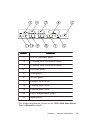
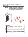
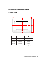
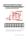
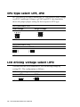
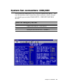
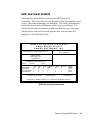
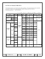
1
TOP-2000
Industrial Panel PC
User’s Manual
CONTENTS
I.
General Information
(i) Product brief
(ii) Specification
(iii) Ordering information for TOP-2000 & spare parts
II.
Panel PC Installation
(i) General information
(ii) System installation
III.
Main board
(i)
(ii)
(iii)
(iv)
(v)
(vi)
IV.
(i)
(ii)
(iii)
(iv)
(v)
General information
Installation
Ethernet
Flat Panel/CRT controller display drivers and utility
Award BIOS setup
Appendix A: Programming the Watchdog Timer
Spare part specification
LCD
Touch screen
Power supply
HDD
FDD
APPENDIX A:
APPENDIX B:
Environmental test report
Spare parts maintenance schedule
PROFESSIONAL FLAT PANEL COMPUTER
DESIGNED TO MEET THE EXTREMELY HIGH
INDUSTRIAL STANDARDS
TOP-2000 Flat Panel Computer is designed to operate in industrial environment which is
characterized by extreme temperature, contaminants, shock, vibration and wide fluctuations
of input power.
HIGHLIGHTS
! Intelligent Temperature Control
! Shock-proof hard disk mobile
module
! Galvanic isolation on I/O ports
! Impact-resistance mechanism
! High protection against corrosion
! Liquid-proof front panel to meet IP-65,
NEMA 4/12
INTELLIGNET TEMPERATURE CONTROL
Intelligent Temperature Control regulates the system temperature in an advanced way.
Temperature is always controlled at a normal level. In the situation of excessive heat, the
system itself will recover quickly from abnormal temperature without system halt.
! Alarm and self-recovery from abnormal temperature
! Automatic turn on of spare fan and slowing down of CPU
! Temperature upper limit setting and monitoring for both system and CPU
SHOCK-PROOF HARD DISK MOBILE MODULE(patented)
Shock-proof hard disk mobile module includes one anti-vibration container and one mobile
carrier. The anti-vibration container with numbers of leaf springs resolves vibration from all
directions – top, bottom, front, rear, right and left. The mobile carrier allows easy
maintenance, easy upgrade and fast access to the system. Two Springs-loaded Panel
Fasteners sitting on the door of Shock-proof hard disk mobile module grant quick access to
LED INDICATOR
! Keep track of the system status including Power, CPU fan, Aux. fans,
Temperature and LAN .
INDIVIDUAL GALVANIC ISOLATION ON I/O PORTS
! 8KV ESD Protection.
! High protection against electrical shocks and transients.
Specification
TOP-2000
Processor
System Memory
Video Controller
Display Memory
Cache
LCD
Expansion Slots
Operating
PC Unit
Temperature LCD Panel
Relative Humidity
EMC, Safety
Industrial Front Panel
Pentium MMX 133-233 or compatible
8-128MB SIMM or DIMM
PCI based SVGA controller C&T 65554
2MB
on-board 512KB
10.4" color TFT 640x480 250 cd/m2
12.1" color TFT 800x600 250 cd/m2
15" color TFT 1024x768 200 cd/m2
Infrared (Citron), Resistive(MicroTouch)
2xRS-232, 2xRS-232/422/485 configurable
galvanic isolation individually
one multi-mode SPP/ECP/EPP parallel port with galvanic isolation
10/100BaseT auto-sensing fast ethernet port
2 USB ports.
One PS/2 mouse and one keyboard ports.
2.5" industrial grade HDD.
M-system DiskOnChip 2MB-72MB
3.5" slim line FDD
90W power 90-264VAC input, +5V@12A, +12V@1A, [email protected]
100W power 18-36VDC input, +5V@15A, +12V@2A
2xISA or 1xPCI, 1xISA
-25
0
5-85% non-condensing
CE
IP65, NEMA 4/12
Construction
Vibration (Operating)
Shock (Operating)
Inside/outside heavy stainless steel.
1G peak(5-500Hz)
20G, 11ms, Half sine wave, 6-axis.
Dimension(WxHxD) (mm)
Model
T2-10AIC, T2-10ARC
T2-10DIC, T2-10DRC
T2-12AIC, T2-12ARC
T2-12DIC, T2-12DRC
T2-15AIC
T2-15DIC
Touch Screen(Optional)
COM port
Parallel port
LAN
USB
PS/2 port
HDD
Solid State Disk(Optional)
FDD
Power Supply
Dimension
378.6x315.6x188.0
378.6x315.6x171.0
404.0x329.6x188.0
404.0x329.6x171.0
508.0x398.0x188.0
508.0x398.0x171.0
TOP-2000 Panel PCs part number list
Part no.
Part no.
Part no.
Part no.
T2-10ARO-1
T2-10AIO-1
T2-10DRO-1
T2-10DIO-1
T2-12ARO-1
T2-12AIO-1
T2-12DRO-1
T2-12DIO-1
T2-15DIO-1
T2-10ARC-1
T2-10AIC-1
T2-10DRC-1
T2-10DIC-1
T2-12ARC-1
T2-12AIC-1
T2-12DRC-1
T2-12DIC-1
T2-15DIC-1
T2-10ARO-2
T2-10AIO-2
T2-10DRO-2
T2-10DIO-2
T2-12ARO-2
T2-12AIO-2
T2-12DRO-2
T2-12DIO-2
T2-15DIO-2
T2-10ARC-2
T2-10AIC-2
T2-10DRC-2
T2-10DIC-2
T2-12ARC-2
T2-12AIC-2
T2-12DRC-2
T2-12DIC-2
T2-15DIC-2
Pre-loaded software
Description
Part no.
E-WIN95
E-WIN98
E-WINNT40
Pre-loaded EWin95/98 and TOP-2000 drivers
Pre-loaded EWin95/98 and TOP-2000 drivers
Pre-loaded EWinNT 4.0 and TOP-2000 drivers
Ordering information
T2
TOP-2000
10
10: 10.4"TFT
12: 12.1"TFT
15: 15.1"TFT
A
R
A: AC power R: Res touch
D: DC power I: IR touch
C
C: close frame
O: open frame
1
( Part number )
config.1: Pentium233, RAM64MB, HDD3.2GB
config.2: Pentium233, RAM128MB,HDD3.2GB
***** CPU, RAM, HDD, Expansion module are optional only when single shipment is above 20 units ******
Spare part list for TOP-2000 PANEL PCs
Part number
T2-LCD-1
T2-LCD-2
T2-LCD-3
T2-INV-1
T2-INV-2
T2-INV-3
T2-CAB-1
T2-CAB-2
T2-CAB-3
T2-IRT-1
T2-IRT-2
T2-IRT-3
T2-MB-1
T2-DCP-1
T2-ACP-1
T2-FAN-1
T2-HDD-1
T2-HDD-2
T2-FDD-1
T2-CPU-1
T2-RAM-1
T2-120-1
Other
Description
10.4" TFT LCD
12.1" TFT LCD
15.1" TFT LCD
10.4" inverter
12.1" inverter
15.1" inverter
10.4" LCD cable
12.1" LCD cable
15.1" LCD cable
10.4" IR touch
12.1" IR touch
15.1" IR touch
Main board MB-564
DC power module
AC power supply
Fan module (3 pcs of Fan + Fan metal holder)
HDD 3.2GB 2.5"
HDD 3.2GB 2.5" with holder
FDD slim line
CPU Pentium-233+ Heat sink + FAN
RAM 128MB
LS-120 drive
Remark
TOP-2000
Installation Manual
Contents
Chapter 1: General Informaion............. 1
Overview ................................................................................ 2
Features .................................................................................. 3
General specifications .......................................................... 3
Power supply .......................................................................... 5
AC input ................................................................................... 5
DC input ................................................................................... 5
Environmental specifications .............................................. 6
Touch screens ........................................................................ 6
Infrared touch type ................................................................... 6
Analog Resistive type ............................................................... 6
Front panel ............................................................................. 7
system staturs indicator ............................................................ 7
Touch screen Driver and user's manual ................................... 8
Cooling system ...................................................................... 9
Power input and power switch ................................................ 10
(1) For DC nput model ............................................................ 10
(2) For AC input model ........................................................... 11
I/O ports and peripherals ................................................... 12
Chapter 2: System Installation .......... 15
Install Add-on Card in TOP-2000 .................................... 16
Step A : Remove the following items ...................................... 17
Step B : Insert your add-on card in system .............................17
Step C : Secure your add-on card ........................................... 17
Replacing filters .................................................................. 18
Install/Maintain hard disk drive ....................................... 19
Outside view of TOP-2000 ................................................ 20
TOP-2000 without aluminum frame (open frame) .................. 20
(1) Front view .......................................................................... 20
(2) Back view .......................................................................... 21
(3) Bottom view ...................................................................... 22
TOP-2000 with aluminum frame ....................................... 23
(1) Front view .......................................................................... 23
(2) Back view .......................................................................... 24
(3) Bottom view ...................................................................... 25
Install TOP-2000 with aluminim frame in your system .....
................................................................................................ 26
Cut-out for TOP-2000 with aluminum frame in your panel ... 26
Installation ............................................................................... 27
Install TOP-2000 without (open frame) aluminim frame
in your system ...................................................................... 29
Cut-out for TOP-2000 with aluminum frame in your panel .... 29
Installation ............................................................................... 30
CHAPTER
General
Information
1
Chapter 1 General Information
1
Overview
Item
1
2
3
2
Name
Display Unit.
PC Unit.
Expansion Unit.
TOP-2000 Installation Manual
Features
• Intelligent System Temperature Control.
• • Infrared/Resistive touch screen.
• • Shockproof hard disk mobile module.
• • Isolation on I/O ports.
• • Liquid-proof and dust-proof in front panel. Meet IP65/NEMA 4/12
standard.
• • Expansion capabilities: two ISA or one PCI , one ISA.
• • Networking: On-board 10/100BaseT auto-sensing Fast Ethernet port.
General specifications
• Construction:
Inside/outside heavy duty stainless steel.
• Cooling system: Three 11.5 CFM(flow-out) fans.
• CPU :
Pentium MMX 133-233 or compatible.
• System Memory: 8-128MB SIMM or DIMM.
• LCD display panel:
Si z e
10.4"
12.1"
15"
Display Type
Color TFT
Color TFT
Color TFT
Resolution
640 x 480
800 x 600
1024 x 768
250
250
200
Luminance (cd/m2)
Chapter 1 General Information
3
• I/O ports:
Four COM ports (2xRS-232, 2x232/422/ 485).
One parallel port.
Two USB ports.
One PS/ 2 mouse and keyboard interface.
One VGA output connector.
10/100MHz fast LAN.
• HDD: EIDE HDD interface (2.5" industrial grade).
• FDD: 3.5" slim line FDD.
• Expansion capabilities: two ISA or one PCI, one ISA.
• Dimensions (WxHxD) (mm):
Mo d el
4
D i m en s i o n
T2-10AIC , T2-10ARC
378.6 x 315.6 x 188.0
T2-10D IC , T2-10D RC
378.6 x 315.6 x 171.0
T2-12AIC , T2-12ARC
404.0 x 329.6 x 188.0
T2-12D IC , T2-12D RC
404.0 x 329.6 x 171.0
T2-15AIC
508.0 x 398.0 x 188.0
T2-15D IC
508.0 x 398.0 x 171.0
TOP-2000 Installation Manual
Power supply
AC input:
Input Voltage: 90-264Vac@47-63HZ.
OutputVoltage: +5V@12A, +12V@1A, [email protected]
Output Power: 90W(MAX)
Safety: Meets UL, CSA, CE
EMC: Meets CE/FCC Class B
MTBF: 100,000 hrs.
DC input:
Input voltage: 18-36Vdc
Output voltage: +5v@15A, +12V@2A
Output power: 100W(max)
MTBF: 100,000 hrs.
Chapter 1 General Information
5
Environmental specifications
•
•
•
•
•
Operating temperature: 0 to 50 OC.
Relative humidity: 5-85% non-condensing.
EMC: CE.
Shock (Operating): 20G, 11ms, Half sine wave, 6-axis.
Vibration (Operating): 1G peak(5-500Hz).
Touch screens
Infrared touch type
• Touch-point density: 16tps/cm2 physical, 64tps/cm2
interpolated.
• Response time: 2.5-6.5ms(software programmable).
• Light Transmission: 100%.
• Touch sensor life: unlimited.
• MTBF-controller: >500000 hrs.
• Controller: RS-232 interface.
• Power consumption: 5V@219mA(max).
Analog resistive type
• Resolution: 1024 touch points per axis within the
calibrated area.
• Response time: 8-15ms.
• Light Transmission: 80%.
• Touch sensor life: >35 million touches.
• MTBF-controller: >500000 hrs.
• Controller: RS-232 interface.
• Power consumption: 5V@70mA(typical).
6
TOP-2000 Installation Manual
Front panel
Item
1
*2
3
Name
LCD panel and Touch screen
System status indicator
Aluminum panel
* For further information, please read section " System
status indicator".
System status indicator
Chapter 1 General Information
7
It em
N am e
Ac t i v e
Co lo r
S t at u s
1
Power
Green System Power On
2
C P U F an
Green Operating
3
AUX Fan
Green Operating
4
HDD
Green Operating
*5
Low Temp.
Green
*6
High Temp.
Red
Lan
Flash Operating
7
System temperature is in
normal temperature level
System temperature is in
abnormal temperature level
* The warning temperature is determined in CMOS setup,
Please refer to "Chipset feature setup" in TOP-2000 Main
Board User's Manual.
Touch screen driver and user's manual
(1) Infrared type touch screen:
For further information, please see the user's manual in \CITRON
directory of the TOP-2000 driver and utility disk CD-ROM for
detail.
(2) Resistive type touch screen:
For further information, please see the user's manual in \MICROTOUCH directory of the TOP-2000 driver and utility disk CD-ROM
for detail.
8
TOP-2000 Installation Manual
Cooling system
It em
N am e
N o r m al S t at u s
1,3
System Fan
Operating
*2
Auxiliary Fan
Controlled by BIOS setting
* For further information, please see the TOP-2000 Main Board
User's Manual for detail.
Chapter 1 General Information
9
Power input and power switch
It em
*1
2
3, 4
N am e
Power i nput connector
Power swi tch
Fi lter
* (1) For DC input model:
Pin 1, 2 : Ground
Pin 4, 5 : DC 18-36 Volts
10
TOP-2000 Installation Manual
* (2) For AC input model:
Pin 1, 3 : AC line in
Pin 2
: Earth ground
Chapter 1 General Information
11
I/O ports and peripherals
It em
12
N am e
1
Floppy disk drive
2
Hard disk drive
3
I/O ports
4
Add-on card slot in expansion unit
TOP-2000 Installation Manual
It em
1
N am e
PS/2 mouse port
*2
C OM4 RS-422/RS-485
*3
C OM3 RS-422/RS-485
4
Pri nter port
5
Lan port
6
VGA port
7
C OM1 RS-232
*8
C OM3 RS-232
*9
C OM4 RS-232
10
PS/2 keyboard port
11
USB port
* For further information, please see the TOP-2000 Main Board
User's Manual for detail.
Chapter 1 General Information
13
14
TOP-2000 Installation Manual
CHAPTER
2
System Installation
Chapter 2 System Installation 15
Install Add-on Card in TOP-2000
Step A : Remove the following items.
Step B : Insert your add-on card in
system
16 TOP-2000 Installation Manual
Step C : Secure your add-on card
Chapter 2 System Installation 17
Replace filters
* You can find four filters in the TOP-2000 accessory box.
18 TOP-2000 Installation Manual
Install / Maintain hard disk drive in
TOP-2000
Warring
Disclaimer : HDD is a highly sensitive device,
thus installation can only be handled by authorized personnel. Any damage results from
improper installation by unauthorized personnel is
not claimbable”.
C omments
A
HD D module should be installed carefully wtih
correct orientation.
B
HD D door can be removed / closed manually or by
screw driver.
C
Slide HD D module along the rail in HD D bay until
the end is reached. Push two black plastic ejectors
toward the unit by both hands gently and carefully to
set HD D in final position.
Chapter 2 System Installation 19
Outside view of TOP-2000
TOP-2000 without aluminum frame (open
frame)
(1) Front view
Si z e
A
B
15.1"
490.0
380.0
12.1"
386.6
311.6
10.4"
360.6
297.6
(Unit: mm)
20 TOP-2000 Installation Manual
(2) Back view
D
E
F
G
H
I
15.1"
178.0
178.0 233.0
233.0
312.0
432.0
12.1"
146.5
146.5
184.0
184.0 264.0
341.0
10.4"
139.5
139.5
171.0
171.0 240.0
315.0
(Unit: mm)
Chapter 2 System Installation 21
(3) Bottom view
J
K
L
M
N
O
15.1"
52.0
AC=94.0
DC=77.0
38.0
AC=184.0
DC=167.0
265.0
83.6
12.1"
52.0
AC=94.0
DC=77.0
38.0
AC=184.0
DC=167.0
265.0
63.0
10.4"
52.0
AC=94.0
DC=77.0
38.0
AC=184.0
DC=167.0
265.0
50.0
(Unit: mm)
22 TOP-2000 Installation Manual
TOP-2000 with aluminum frame
(1) Front view
A
B
15.1"
508.0
398.0
12.1"
404.0
329.6
10.4"
378.6
315.6
(Unit: mm)
Chapter 2 System Installation 23
(2) Back view
D
E
F
G
H
I
15.1"
178.0
178.0 233.0
233.0
312.0
432.0
12.1"
146.5
146.5
184.0
184.0 264.0
341.0
10.4"
139.5
139.5
171.0
171.0 240.0
315.0
(Unit: mm)
24 TOP-2000 Installation Manual
(3) Bottom view
J
K
L
M
N
O
15.1"
52.0
AC=94.0
DC=77.0
38.0
AC=184.0
DC=167.0
265.0
83.6
12.1"
52.0
AC=94.0
DC=77.0
38.0
AC=184.0
DC=167.0
265.0
63.0
10.4"
52.0
AC=94.0
DC=77.0
38.0
AC=184.0
DC=167.0
265.0
50.0
(Unit: mm)
Chapter 2 System Installation 25
Install TOP-2000 with aluminum frame
in your system
Cut-out for a TOP-2000 with aluminum frame
in your panel.
A
B
C
D
E
F
F1
G
H
15.1" 233.0 233.0 178.0 178.0 435.0 327.0
157.5
446.0
164.0
80.0
Φ 6.0
Φ 8.0
80.0
12.1"
184.0 184.0 146.5 146.5 344.0 275.0
133.5
351.0
137.0
70.0
Φ 6.0
Φ 8.0
60.0
10.4"
171.0 171.0 139.5 139.5 318.0 252.0
121.5
325.0
125.0
70.0
Φ 6.0
Φ 8.0
60.0
H1 - H4 J (x8) K (x11) W1 - W4
(Unit: mm)
26 TOP-2000 Installation Manual
Installation
(1)
(2)
Chapter 2 System Installation 27
C o m m en t s
A
(1) #10 washer, M4 nut.
(2) You can fi nd them i n the TOP-2000
accessory box.
28 TOP-2000 Installation Manual
Install TOP-2000 without aluminum
frame (open frame) in your system
Cut-out for a TOP-2000 without aluminum
frame (open frame) in your panel.
A
B
C
D
E
F
G*
233.0
233.0
178.0
178.0
345.0
268.0
M4x30
12.1"
184.0
184.0
146.5
146.5
284.0
223.0
M4x30
10.4"
171.0
171.0
139.5
139.5
249.0
196.0
M4x30
15.1"
(Unit: mm)
* To mount open frame TOP-2000, you need to plant M4x30 bolts
with thread in the wall as shown in the cut-out drawing.
Chapter 2 System Installation 29
Installation
(1)
(2)
30 TOP-2000 Installation Manual
C o m m en t s
A
(1) #10 washer, M4 nut.
(2) You can fi nd them i n the TOP-2000
accessory box.
(3)
Chapter 2 System Installation 31
(4)
C o m m en t s
A
The gap between TOP-2000 and wall must be sealed
carefully to repel water and dust.
32 TOP-2000 Installation Manual
TOP-2000 Main Board
User's Manual
FCC STATEMENT
THIS DEVICE COMPLIES WITH PART 15 FCC RULES. OPERATION IS SUBJECT TO THE FOLLOWING TWO CONDITIONS:
(1) THIS DEVICE MAY NOT CAUSE HARMFUL INTERFERENCE. (2) THIS DEVICE MUST ACCEPT ANY INTERFERENCE
RECEIVED, INCLUDING INTERFERENCE THAT MAY CAUSE
UNDESIRED OPERATION.
THIS EQUIPMENT HAS BEEN TESTED AND FOUND TO
COMPLY WITH THE LIMITS FOR A CLASS "A" DIGITAL
DEVICE, PURSUANT TO PART 15 OF THE FCC RULES.
THESE LIMITS ARE DESIGNED TO PROVIDE REASONABLE PROTECTION AGAINST HARMFUL INTERFERENCE
WHEN THE EQUIPMENT IS OPERATED IN A COMMERCIAL ENVIRONMENT. THIS EQUIPMENT GENERATES,
USES, AND CAN RADIATE RADIO FREQUENCY ENERGY
AND , IF NOT INSTALLED AND USED IN ACCORDANCE
WITH THE INSTRUCTION MANUAL, MAY CAUSE
HARMFUL INTERFERENCE TO RADIO COMMUNICATIONS. OPERATION OF THIS EQUIPMENT IN A RESIDENTIAL AREA IS LIKELY TO CAUSE HARMFUL INTERFERENCE IN WHICH CASE THE USER WILL BE REQUIRED
TO CORRECT THE INTERFERENCE AT HIS OWN EXPENSE.
Copyright Notice
This document is copyrighted, 1999. All rights are reserved. The
original manufacturer reserves the right to make improvements to
the products described in this manual at any time without notice.
No part of this manual may be reproduced, copied, translated or
transmitted in any form or by any means without the prior written
permission of the original manufacturer. Information provided in
this manual is intended to be accurate and reliable. However, the
original manufacturer assumes no responsibility for its use, nor for
any infringements upon the rights of third parties which may result
from its use.
Acknowledgements
VIA is a trademark of VIA Technology, Inc.
AMD is a trademark of Advanced Micro Devices, Inc.
Award is a trademark of Award Software International, Inc.
Cyrix is a trademark of Cyrix Corporation.
IBM, PC/AT, PS/2 and VGA are trademarks of International
Business Machines Corporation.
Intel Pentium and MMX are trademarks of Intel Corporation.
Microsoft Windows ® is a registered trademark of Microsoft Corp.
SMC is a trademark of Standard Microsystems Corporation.
RTL is a trademark of Realtek Semi-Conductor Co., Ltd.
C&T is a trademark of Chips and Technologies, Inc.
UMC is a trademark of United Microelectronics Corporation.
All other product names or trademarks are properties of their
respective owners.
TOP-2000 Main Board User's Manual 1nd Edition
April 1999
Contents
Chapter 1: General Information ........... 1
Introduction ........................................................................... 2
Features .................................................................................. 3
Specifications ......................................................................... 4
Board dimensions ................................................................. 6
Chapter 2: Installation ...................... 7
Jumpers and connectors ...................................................... 8
Locating jumpers and connectors .................................... 10
Setting jumpers ................................................................... 11
CPU installing and upgrading ............................................ 12
System clock setting (SW1-1, 2, 3) ......................................... 13
CPU frequency ratio (SW1-4, 5, 6) ........................................ 13
CPU voltage setting (SW2) ..................................................... 14
Installing DRAM (SIMM1, SIMM2, DIMM1) ............. 15
Installing SIMM & DIMM ...................................................... 15
DiskOnChip memory address select (SW3) ................... 16
Clear CMOS (JP1) ............................................................. 17
PCI clock setting (JP2) ...................................................... 17
CPU type select (JP3, JP4) ............................................... 18
LCD driving voltage select (JP5) ..................................... 18
USB connector (USB1, USB2)(CN1) ............................... 19
Power connectors (CN2) .................................................... 19
Keyboard and PS/2 mouse connector (CN3) .................. 20
IDE hard drive connector (CN5, CN4) ............................ 21
Serial ports (CN11, CN23, CN10, CN6) .......................... 22
System fan connector (CN8, CN9) ................................... 23
Display connectors (CN11, CN20) ................................... 24
CPU fan connector (CN12) ................................................ 26
Ethernet configuration (CN26) ......................................... 27
Ethernet 100/10BASE-T connector (CN13) ........................... 27
Reset switch (CN14) .......................................................... 28
IrDA connector (CN16) ..................................................... 28
Digital I/O connector (CN17) ............................................ 29
LCD backlight control (CN19) .......................................... 29
System speaker (CN21) ..................................................... 30
Floppy drive connector (CN24, CN25) ............................ 31
Connecting the floppy drive .....................................................31
DiskOnChip socket (U11) ................................................. 32
Chapter 3: Ethernet........................... 33
Ethernet Driver Disk ......................................................... 34
Chapter 4: Flat Panel/CRT Controller
Display Drivers and Utilities .......... 35
Software driversand utilities .............................................. 36
Chapter 5: Award BIOS setup ............ 37
System test and initialization ............................................. 38
System configuration verification ............................................ 38
AWARD BIOS setup ........................................................... 39
Entering setup .......................................................................... 39
Standard CMOS setup ....................................................... 40
BIOS features setup................................................................ 41
Virus warning .......................................................................... 41
CHIPSET features setup ........................................................ 44
Power management setup ....................................................... 48
PnP/PCI configuration ............................................................ 52
Integrated Peripherals ............................................................. 54
Load BIOS defaults / Load setup defaults .............................. 56
Change password .................................................................... 57
Auto detect hard disk .............................................................. 58
HDD low level format............................................................. 59
Save & exit setup .................................................................... 60
Exit without saving .................................................................. 60
Appendix A: Programming the Watchdog
Timer ............................................. 61
Programming the watchdog timer .................................... 62
CHAPTER
General
Information
1
This chapter gives background information on the TOP-2000 Main Board.
Sections include:
• Specifications
• Layout and dimensions
Chapter 1 General Information
1
Introduction
The TOP-2000 Main Board is an all-in-one LPX Pentium MMX
computer with an on-board PCI SVGA controller, a PCI Ethernet
interface and a PISA expansion slot (one dedicated EISA slot for PCI/
ISA riser card option). Equipped with 64 bits and local bus architecture, the TOP-2000 Main Board releases Pentium's full potential and
provides unprecedented performance compared to current 32-bit
processor boards. Supports Intel Pentium P54C/P55C(MMX), AMD
K5/K6, and Cyrix M1/M2 CPUs. The TOP-2000 Main Board offers all
the functions of an industrial computer on a single board, but fits in
the space of LPX form factor (only 225mm x 220mm). For maximum
performance, the TOP-2000 Main Board also supports 2nd level cache
sized 512 KB.
On-board features include four serial ports (Two RS-232 and two RS232/422/485), one multi-mode parallel (ECP/EPP/SPP) port, a floppy
drive controller, a keyboard and a PS/2 mouse interface. The built-in
high-speed PCI IDE controller supports both PIO bus master and Ultra
DMA/33 modes. Up to four IDE devices can be connected, including
hard disks, CD-ROM drives, tape backup drives, and other IDE
devices.
The TOP-2000 Main Board also features power management to
minimize power consumption. It complies with the Green Function”
standard and supports three types of power-saving features: Doze
mode, Standby mode, and Suspend mode. In addition, the board’s
watchdog timer can automatically reset the system or generate an
interrupt in case the system stops due to a program bug or EMI.
On-board peripherals with true PCI
performance
The TOP-2000 Main Board is a highly integrated, all-in-one LPX
computer. All on-board peripherals (including PCI flat panel/VGA
interface, PCI Ethernet, and PCI IDE) adopt PCI technology and
operate through an internal PCI bus. Integrating a Pentium board with
PCI architecture has unleashed a revolutionary level of performance.
2
TOP-2000 Main Board User's Manual
Features
• Accepts Intel Pentium P54C/P55C 75-233 MHz, AMD K5 PR75~166, K6 PR2
166~300, Cyrix/IBM/SGS 6x86 PR100+~166+ and M2 CPUs
• Award Flash BIOS, Flat-Panel configured by programming Flash chip
• 2nd level cache: supports Pipeline burst RAM module, 512 KB cache
memory
• 32-bit PCI-bus SVGA controller, supports flat panel (TFT, STN, mono and
EL) and CRT displays
• 10/100 Mbps auto-sense Ethernet LAN controller RTL8139A
• One PISA slot for PCI/ISA riser card
• Built-in, bus-master PCI IDE controller supports both PIO bus master and
Ultra DMA/33 mode up to four IDE devices (hard disk, CD-ROM, tape
backup, etc.)
• Supports both common and EDO type DRAM, from 8 MB to 128 MB of
DRAM
• One 168-pin SDRAM socket
• Two USB ports on board
• One 32-pin DIP socket supports M-system Disk-On-Chip 2000 series,
memory capacity from 2 MB to 72 MB
• One enhanced multi-mode SPP/EPP/ECP parallel port, four serial ports: two
RS-232 and two RS-232/422/485 selectable
• Green function: supports doze/standby/suspend modes
• Intel ligent temperature control
• LCD backlight control
• Dimensions: 225mm x 220mm
Chapter 1 General Information
3
Specifications
Standard MB functions
CPU: Intel Pentium P54C/P55C(MMX) 75-233 MHz,
Cyrix / IBM / SGS 6X86 100+~166+, M2,
AMD K5 PR75~166, K6 PR2 166 ~300 MHz
BIOS: Award 256KB FLASH BIOS
Chipset: SiS 5582
Super I/O: UM8663, UM8661
Cache memory: On board 512 KB pipeline burst RAM 2nd level cache
RAM memory: 8MB to 128MB. Two 72-pin SIMM socket on board,
one 168-pin SDRAM socket
IDE hard disk drive interface: Supports both PIO bus master and Ultra
DMA/33 mode up to four IDE (AT bus) drives. BIOS auto-detect.
(44 pin, patch 2.0mm connector x 1; 40 pin, pitch 2.54mm connector x 1)
Floppy disk drive interface: Supports up to two floppy disk drives,
5.25" (360KB and 1.2MB) and/or 3.5" (720KB, 1.44MB, and 2.88MB)
Multi-mode parallel port: Configured to LPT1, LPT2, LPT3 or disabled.
Supports SPP, ECP, and EPP.
Serial ports: Two RS-232 and two RS-232/422/485 serial ports. Ports
can be configured as COM1, COM2, COM3, COM4, or disabled
individually. Four 16C550 serial UARTs.
DMA channels: 7
Interrupt levels: 15
Keyboard/mouse connector: 6 pin mini DIN connector x 2, support
standard keyboard and P/S2 mouse.
USB ports: Two USB ports on board.
Real Time Clock/Calendar: quartz oscillator, powered by lithium
battery for data retention of up to 10 years.
Power management: I/O peripheral devices support power saving and
Doze/Standby/Suspend modes. AMP 1.2 compliant.
4
TOP-2000 Main Board User's Manual
Flat panel VGA interface (PCI Bus)
Chipset: C&T 65554
Display memory: 2MB
Display type: Supports CRT and flat panel (TFT, DSTN, mono and EL)
display. Can display both CRT and flat panel simultaneously.
Resolution: 1024x768@64K colors
Ethernet interface (PCI Bus)
Chipset: Realtek 8139A PCI bus Ethernet controller.
SSD interface
One 32-pin DIP socket supports M-system Disk-On-Chip 2000 series,
memory capacity from 2MB to 72MB.
Expansion slots
PISA slot: One dedicated PISA slot for PCI/ISA riser card
Mechanical and environmental
Power supply voltage: +5V (4.75V to 5.25V)
Max. power requirements:
Bare Board: +5V @ 1.5A
Pentium MMX: +5V @ 6A
AMD K6-233: +5V @ 10A
Operating temperature: 32 to 140o F (0 to 60o C)
Board Size: 225mm (L) x 220mm (W)
Weight: 1.1 lb. (0.5 Kg)
Chapter 1 General Information
5
Board dimensions
41.63
43.38
30.23
180.3
8.65
139.5
Dimensions in mm
TOP-2000 Main Board dimensions
6
TOP-2000 Main Board User's Manual
CHAPTER
Installation
2
This chapter describs how to set up the
mainboard hardware, including instructions on setting jumpers and connecting
peripherals, switches, and indicators. Be
sure to read all the safety precautions
before you begin the installation procedure.
Chapter 2 Installation 7
Jumpers and connectors
Connectors on the board link them to external devices such as hard
disk drives, a keyboard, or floppy drives. In addition, the board has a
number of jumpers that allow you to configure your system to suit
your application.
The table below lists the function of each of the board's jumpers and
connectors.
DIP Switches
Label
SW1 (1,2,3)
SW1 (4,5,6)
SW2 (1,2)
SW2 (3,4)
SW2 (5,6,7)
SW4
Function
System clock setting
CPU frequency ratio
RS-232,422,485 selection for COM3
RS-232,422,485 selection for COM4
DiskOnChip memory address setting
CPU voltage setting
Jumpers
label
JP1
JP2
JP3,JP4
JP5
Function
Clear CMOS
PCI clock setting
CPU type selection
LCD 5V/3.3V selection
8 TOP-2000 Main Board User's Manual
Connectors
label
CN1
CN2
CN3
CN4
CN5
CN6
CN7
CN8,9
CN10
CN11
CN12
CN26
CN14
CN16
CN17
CN18
CN19
CN20
CN21
CN22
CN23
CN24
CN25
Function
USB
POWER
Keyboard / Mouse
Secondary IDE
Primary IDE
COM4
EISA bus ( ISA/PCI )
System fans
COM3
COM1/ Printer port/ VGA
CPU fan
10/100BaseT Ethernet RJ-45
Reset
IrDA
Digital I/O (bit 0~3)
System status LED
Back light control
LCD interface
Buzzer / speaker
Keyboard lock
COM2
slim FDD
FDD
Chapter 2 Installation 9
Locating jumpers and connectors
JP1
CN2
SIMM1
CN1
SIMM2
DIMM1
CN4
CN3
BIOS
U11
CN6
CN5
SiS
5582
1 2 3 4 5 6
CN9
CN10
ON
ON
SW1
SW1
1 2 3 4
CN8
SW1
ON
SW1
1 2 3 4
CN11
JP3
Socket
Digital
21143
CHIPS
B65554
CN26
JP4
CN12
CN18
CN15
CN14
CN24
SW2
CN16 CN17
CN19 JP5
SW4
10 TOP-2000 Main Board User's Manual
JP2
CN20 CN22
CN21 CN23
CN25
Setting jumpers
You configure your card to match the needs of your application by
setting jumpers. A jumper is the simplest kind of electric switch. It
consists of two metal pins and a small metal clip (often protected by a
plastic cover) that slides over the pins to connect them. To close a
jumper, you connect the pins with the clip. To open a jumper, you
remove the clip. Sometimes a jumper will have three pins, labeled 1, 2,
and 3. In this case, you would connect either pins 1 and 2 or 2 and 3.
1
Open
Closed
2
3
Closed 2-3
The jumper settings are schematically depicted in this manual as
follows:
1 2 3
Open
Closed
Closed 2-3
A pair of needle-nose pliers may be helpful when working with
jumpers.
If you have any doubts about the best hardware configuration for
your application, contact your local distributor or sales representative
before you make any changes.
Generally, you simply need a standard cable to make most connections.
Chapter 2 Installation 11
CPU installing and upgrading
You can upgrade to a higher power Pentium CPU at
any time. Simply remove the old CPU, install the new
one, and set the jumpers for the new CPU type and
speed.
Warning! Always disconnect the power cord from your chassis
when you are working on it. Do not make connections
while the power is on, as sensitive electronic components can be damaged by the sudden rush of power.
Only experienced electronics personnel should open
the PC chassis.
Caution!
Always ground yourself to remove any static charge
before touching the PC board. Modern electronic
devices are very sensitive to static electric charges. Use a grounding wrist strap at all times. Place
all electronic components on a static-dissipative
surface or in a static-shielded bag when they are
not in the chassis.
When you install a new CPU, be sure to adjust the board settings,
such as CPU type and CPU clock. Improper settings may damage
the CPU.
12 TOP-2000 Main Board User's Manual
System clock setting (SW1-1, 2, 3)
SW1-1, 2, 3 are used to sychronize the system clock with the CPU
type. You may need to adjust the CPU clock according to the base
CPU speed.
System clock select
50MHz
55MHz
60MHz
66MHz*
75MHz
83MHz
SW1-1
ON
ON
OFF
ON
OFF
ON
SW1-2
ON
ON
ON
OFF
ON
OFF
SW1-3
ON
OFF
ON
ON
OFF
OFF
* Default
CPU frequency ratio (SW1-4, 5, 6)
System frequency
2x
2x
2.5x
3x *
3.5x
4x
4x
4.5x
5.0x
5.5x
SW1-4
ON
ON
OFF
OFF
ON
ON
OFF
OFF
SW1-5
OFF
ON
ON
OFF
OFF
ON
ON
OFF
SW1-6
OFF
OFF
OFF
OFF
ON
ON
ON
ON
Chapter 2 Installation 13
CPU voltage setting (SW4)
SW4 must be set to match the CPU type. The chart below shows the
proper jumper settings for their respective Vcc.
CPU voltage setting (SW4-1, SW4-2, SW4-3, SW4-4)
CPUVcc
SW4-1 SW4-2 SW4-3 SW4-4
2.0V
2.1V
2.2V
2.3V
2.4V
2.5V
2.6V
2.7V
2.8V*
2.9V
3.0V
3.1V
3.2V
3.3V
3.4V
3.5V
* Default
OFF
OFF
OFF
OFF
OFF
OFF
OFF
OFF
ON
ON
ON
ON
ON
ON
ON
ON
14 TOP-2000 Main Board User's Manual
OFF
OFF
OFF
OFF
ON
ON
ON
ON
OFF
OFF
OFF
OFF
ON
ON
ON
ON
OFF
OFF
ON
ON
OFF
OFF
ON
ON
OFF
OFF
ON
ON
OFF
OFF
ON
ON
OFF
ON
OFF
ON
OFF
ON
OFF
ON
OFF
ON
OFF
ON
OFF
ON
OFF
ON
Installing DRAM (SIMM1, SIMM2, DIMM1)
The TOP-2000 Main Board provides two 72-pin SIMM (Single In-line
Memory Module) sockets and one 168-pin DIMM (Dual-in-line
Memory Module). The SIMM supports either Fast Page Mode (FPM)
or Extended Data Output (EDO) DRAM with a speed of at least 70 ns.
The DIMM supported by this mainboard are always 64-bit wide
SDRAM (Synchronous DRAM). Unlike most other CPU cards, the
MB-564 supports both single and dual insertion into the memory bank.
Depending on the combination of modules you use, you can install
from 8 MB to 128 MB of RAM. Please always insert two SIMM or one
DIMM for correct operation. Don't use SIMM and DIMM modules in
one system.
Installing SIMMs & DIMM
NOTE:
The modules can only fit into a socket one way. Their chips
must face the CPU, and their gold pins must point down into
the SIMM socket.
1. Ensure that all power sources are disconnected.
2. Slip the memory module into the socket at a 45 degree angle.
3. Push the module toward the vertical posts at both ends of the
socket until the module is upright and the retaining clips at both
ends of the module click into place. When positioned correctly, the
pins on top of the vertical posts should correspond to the circular
holes on the ends of the module.
4. Repeat steps 2 and 3 for each module you install.
Chapter 2 Installation 15
DiskOnChip memory address select
(SW2)
The DiskOnChip 2000 occupies a 8 Kbyte window in the upper
memory address range of CC00 to E000. You should ensure this dose
not conflict with any other device's memory address.
DiskOnChip 2000 memory address (SW2)
Memory address (HEX)
5
6
CC00
ON
OFF
D000*
ON
OFF
D400
OFF
ON
D800
OFF
ON
DC00
OFF
OFF
E000
OFF
OFF
7
ON
OFF
ON
OFF
ON
OFF
* Default
These addresses might conflict with the ROM BIOS on some of other
peripheral boards. Please select appropriate memory address to avoid
memory conflict.
16 TOP-2000 Main Board User's Manual
Clear CMOS (JP1)
You can connect an external switch to clear CMOS. This switch closes
JP1 and turns on the power, at which time the CMOS setup can be
cleared.
Clear CMOS (JP1)
Protect*
1
2
Clear CMOS
3
1
2
3
* default
PCI clock setting (JP2)
JP2 is used to sychronize the system clock with the CPU clock and PCI
clock. You may need to adjust the CPU clock according to the base
CPU speed.
PCI clock setting (JP2)
PCI clock
32 MHz
1
2
3
1/2 CPU clock*
1
2
3
* Default
Chapter 2 Installation 17
CPU type select (JP3, JP4)
JP3, JP4 must be set both to match the CPU type between Dual-Voltage
(e.g.P55C) and Single-Voltage (e.g.P54C) type CPU. the chart below
shows the proper jumper setting for their respective CPU type.
CPU type select (JP3)
Dual-Voltage*
Single-Voltage
6
4
2
5
3
1
6
4
2
5
3
1
* Default
CPU type select (JP4)
P55C*
1
2
P54C
3
1
2
3
* Default
LCD driving voltage select (JP5)
You can select the LCD connector LCD CON driving voltage by
setting JP5. The configuration as follows:
LCD driving voltage select (JP5)
5V*
3.3V
1 2
3
* Default
18 TOP-2000 Main Board User's Manual
1 2 3
USB connector (USB1, USB2)(CN1)
You can connect your USB (Universal Serial Bus) devices to USB
connector. With USB, there is no need to have separate connectors for
keyboards, modems, and mice. USB provides a common interface for
all your perpherals.
USB connector (USB1, USB2)(CN1)
Pin
Function
Pin
1
Vcc
5
2
UV16
3
UN1 +
7
4
GND
8
Function
Vcc
UV0UV0+
GND
Power connectors (CN2)
AT power connector (CN2)
The following table lists the pin assignments for the Power Connector:
Power Connector (CN2)
pin
Signal
1
PG
2
+5V
3
+12V
4
-12V
5
GND
6
GND
pin
7
8
9
10
11
12
Signal
GND
GND
-5V
+5V
+5V
+5V
Power LED (D1)
The power LED to indicate when the mainboard is on.
Chapter 2 Installation 19
Keyboard and PS/2 mouse connector
(CN3)
The TOP-2000 Main Board provide a keyboard connector and a PS/2
style mouse connector. In most cases, especially in embedded applications, a keyboard is not used. The standard PC/AT BIOS will report an
error or fail during power-on self test (POST) after a reset if the
keyboard is not present. The TOP-2000 Main Board's BIOS standard
setup menu allows you to select "All, But Keyboard" under the "Halt
On" selection. This allows no-keyboard operation in embedded system
applications without the system halting under POST (power-on-selftest).
The upper connector of CN3 is for mouse, the lower one is for keyboard.
20 TOP-2000 Main Board User's Manual
IDE hard drive connector (CN5, CN4)
You can attach one to four Enhanced Integrated Device Electronics
hard disk drives to the TOP-2000 Main Board internal controller. The
TOP-2000 Main Board's IDE controller uses a PCI local-bus interface.
This advanced interface supports faster data transfer and allows the
IDE hard drive to exceed 528 MB.
Connecting the hard drive
Connecting drives is done in a daisy-chain fashion and requires one
of two cables, depending on the drive size. 1.8" and 2.5" drives need a
44-pin to flat-cable connector for CN5(Primary IDE). 3.5" drives use a
40-pin flat-cable for CN4(Secondary IDE).
Wire number 1 on the cable is red or blue, and the other wires are gray.
1. Connect one end of the cable to CN5 or CN4. Make sure that the
red (or blue) wire corresponds to pin 1 on the connector, which is
labeled on the board (on the right side).
2. Plug the other end of the cable to the Enhanced IDE hard drive,
with pin 1 on the cable corresponding to pin 1 on the hard drive.
(See your hard drive's documentation for the location of the
connector.)
Connect a second drive as described above.
Unlike floppy drives, IDE hard drives can connect to either end of the
cable. If you install two drives through one cable, you will need to set
one as the master and one as the slave by using jumpers on the drives.
If you install just one drive, set it as the master.
PIN1
IDE connector
Chapter 2 Installation 21
Serial ports (CN11, CN23, CN10, CN6)
The TOP-2000 Main Board offers four serial ports: two RS-232 (COM1
,COM2, ) and two RS-232/422/485(COM3, COM4). These ports let you
connect to serial devices (a mouse, printers, etc.) or a communication
network.
Configure RS-232/422/485 for COM3, COM4
SW2
1
2
COM3
OFF x
ON OFF
ON ON
x : Don't care
3
4
COM4
OFF x
ON OFF
ON ON
* : Default
RS-232
COM 1,2,3,4 RS-232 ports
pin
Signal
pin
1
DCD
6
2
RX
7
3
TX
8
4
DTR
9
5
GND
Signal
DSR
RTS
CTS
RI
RS-422/485
COM 3,4 RS-422/485 ports
pin
Signal
pin
1
TXD+
6
2
TXD7
3
RXD+
8
4
RXD9
5
GND
22 TOP-2000 Main Board User's Manual
Signal
NC
NC
NC
GND
Function
RS-232*
RS-422
RS-485
System fan connectors (CN8,CN9)
Two system fan connectors (CN8, CN9) are controlled by BIOS. System fan interfaces can be turned on when overheat or can be always
on” which is pre-set in the CMOS SETUP – CHIPSET FEATURES
SETUP.
System fan connectors (CN8,CN9)
Pin
1
2
3
Function
GND (FAN ON/OFF CONTROL)
+12
RPM (ROTATION DETECT SIGNAL)
Chapter 2 Installation 23
Display connectors (CN11, CN20)
The TOP-2000 Main Board's PCI SVGA interface can drive conventional CRT displays through CN11and is capable of driving a wide range of
flat panel displays including electroluminescent (EL), gas plasma,
passive LCD and active LCD displays. The card has two connectors to
support these displays, one for standard CRT VGA monitors and one
for flat panel displays.
The TOP-2000 Main Board's SVGA connector (VGA) with PCI bus
supports monochrome display as well as high resolution color
displays. The card also features a LCD connector (CN20), which allows
you to connect various flat panel displays. The following table lists
pin assignments of CN20:
LCD connector (CN20)
Pin
Function
1
+12VDC
3
GND
5
+5VDC(or 3.3V)
7
EN LCD ( ENAVEE)
9
P0
11
P2
13
P4
15
P6
17
P8
19
P10
21
P12
23
P14
25
P16
27
P18
29
P20
31
P22
33
P24
35
LCD clock (SHFCLK)
37
M
39
GND
41
P26
43
P28
24 TOP-2000 Main Board User's Manual
Pin
2
4
6
8
10
12
14
16
18
20
22
24
26
28
30
32
34
36
38
40
42
44
Function
+12VDC
GND
+5VDC (or 3.3V)
GND
P1
P3
P5
P7
P9
P11
P13
P15
P17
P19
P21
P23
P25
FLM (V SYN)
LP (H SYN)
-blank (ENABKL)
P27
P29
Pin
45
47
49
Function
P30
P32
P34
Pin
46
48
50
Function
P31
P33
P35
SVGA connector (CN11)
Pin
Finction
1
Red video
2
Green video
3
Blue video
4
Not used
5
GND
6
Red return (GND)
7
Green return (GND)
8
Blue return (GND)
9
Key (no pin)
10
Sync return (GND)
11
Monitor ID (not used)
12
Monitor ID
13
Horizontal sync
14
Vertical sync
15
Not used
Chapter 2 Installation 25
CPU fan connector ( CN12 )
CPU fan connectors (CN12)
Pin
1
2
3
Function
GND (FAN ON/OFF CONTROL)
+12V
RPM (ROTATION DETECT SIGNAL)
26 TOP-2000 Main Board User's Manual
Ethernet configuration (CN26)
The mainboard is equipped with a high performance 32-bit PCI-bus
Ethernet interface which is fully compliant with IEEE 802.3 10/100Mbps
CSMA/CD standards. It is supported by all major network operating
systems.
Configuration is very simple and is done via the BIOS setup. The
medium type can be configured via the program included on the utility
disk.
Ethernet 100/10BASE-T connector (CN26)
100/10BASE-T connects to the aminboard via a RJ-45 connector
(CN26).
Ethernet 100/10BASE-T connector (CN26)
Pin
1
2
3
4
5
6
7
8
Signal
TX+
TXRX+
GND
GND
RXGND
GND
Chapter 2 Installation 27
Reset switch (CN14)
You can connect an external switch to easily reset your computer.
This switch restarts your computer as if you had turned off the power
then turned it back on. The following table shows the pin assignments
for RESET SW.
Reset switch (CN14)
Pin
1
2
Function
GND
Reset
IrDA connector (CN16)
The IrDA connector can be configured to support wireless infrared
modul, with this module and application software such as Laplink, user
can transfer file to or form laptops, note book, PDA and printers. The
pin assignment as follows:
IrDA connector (CN16)
Pin
1
2
3
4
5
Function
Vcc
FIR RX
IR Rx
GND
IR Tx
28 TOP-2000 Main Board User's Manual
Digital I/O connector (CN17)
The digital I/O connector provides 4 TTL level input and output pins
for general purpose.
Digital I/O connector (CN17)
Pin
1
2
3
4
294H (I/O port address)
bit 0
bit 1
bit 2
bit 3
LCD backlight control (CN19)
The CN19 is a 5-pin invertor connector which could provide the power
for LCD invertor. The following table is the pin assignment of CN19.
The pin-5 "BKL_ON" is normally active "high". Please refer to "Power
Management Setup" in the BIOS SETUP Menu and select "LCD off
Option" to enable power management.
CN19 offers LCD backlight control signals for your applications. The
pin assignment is as follows:
LCD backlight control (CN19)
PIN
1
2
3
4
5
Function
+12V ENB
GND
VCC
NC
BKL_ON
Chapter 2 Installation 29
System speaker (CN21)
The CPU card has its own buzzer. You can disable the internal buzzer
and connect an external speaker to SPK.
System speaker (CN21)
Pin
Function
1
Vcc
2
Speaker output
3
Buzzer in *
4
Speaker output *
*default: connect a jumper between pin 3 and pin 4 for internal buzzer
output.
30 TOP-2000 Main Board User's Manual
Floppy drive connector (CN24, CN25)
You can attach up to two floppy disks to the TOP-2000 Main Board's onboard controller. You can use any combination of 5.25" (360 KB and 1.2
MB) and/or 3.5" (720 KB, 1.44 MB, and 2.88 MB) drives.
A 34-pin daisy-chain drive connector cable is required for a dual-drive
system. On one end of the cable is a 34-pin flat-cable connector. On the
other end are two sets of floppy disk drive connectors. Each set consists
of a 34-pin flat-cable connector (usually used for 3.5"drives) and a
printed-circuit board connector (usually used for 5.25" rives).
CN24 is for a slim floppy drive. PIN1 of CN24 is shown on the M/B.
Connecting the floppy drive
1. Plug the 34-pin flat-cable connector into CN25 make sure that the red
wire corresponds to pin one on the connector.
2. Attach the appropriate connector on the other end of the cable to the
floppy drive(s). You can use only one connector in the set. The set on
the end (after the twist in the cable) connects to the B: drive. The set
in the middle connects to the A: drive.
3. If you are connecting a 5.25" floppy drive, line up the slot in the
printed circuit board with the blocked-off part of the cable connector.
If you are connecting a 3.5" floppy drive, you may have trouble
determining which pin is pin number one. Look for a number printed
on the circuit board indicating pin number one. Also, the connector
on the floppy drive connector may have a slot. When the slot is up,
pin number one should be on the right. Check the documentation that
came with the drive for more information.
Chapter 2 Installation 31
DiskOnChip socket (U11)
The DiskOnChip 2000 family of products provides a single chip
solid-state flash disk in a standard 32-pin DIP package. The
DiskOnChip 2000 is a solid-state disk with no moving parts,
resulting in a significant reduction in power consumption and an
increase in reliability. The DiskOnChip is small, plug and play Flash
disk. It is easy to use and saves integration overhead.
The DiskOnChip 2000 family of products is available in capacities
ranging from 2MB up to 72 MB, unformatted. This way, the same
socket on the target platform will not have to be changed. In order
to manage the disk, the DiskOnChip 2000 includes the TrueFFS, MSystems' Flash File System proprietary software. The DiskOnChip
2000 package is pin-to-pin compatible with standard 32-pin EPROM
device.
pin
Name
Descr iption
Pin N umber
Dir ection
A0-A12
Addr ess bus
4- 12,23,25-27
Inputs
A13-A16
Addr ess bus
2,3,28,29
Inputs
D0- D7
Data bus
13- 15,17-21
I/O
CE/
C hip Enable
22
Input
OE/
Output Enable
24
Input
WE/
Wr ite Enable
31
Input
NC
Not connected
1.30
VCC
Pow er
32
GND
Ground
16
Note
1
OE /
Figure1-MD2200 Pin-out
Note 1:Pins A13 through A16 are not used
by the MD2200. They are kept for socket
backward compatibility with ED 1100
(DiskOnChip 1000)
Note 2:Pins 1 and 30 are not used by
MD2200
32 TOP-2000 Main Board User's Manual
2
CHAPTER
Ethernet
3
This chapter shows what is inside the
Ethernet disk and which web site to
connect for more information or driver
download.
Chapter 3 Software Configuration
33
Ethernet Driver in TOP-2000 Driver CD
The TOP-2000 Driver CD includes Microsoft network drivers for
--- Windows for Workgroups 3.1
--- Windows 95 & OSR2
--- Windows NT 3.5, 3.51, 4.0
The Ethenet drivers are in the directory
\TOP2000_driver&utilities\Main board\Ethernet chip
For other information or to download other drivers,please connect
http:///www.realtek.com.tw/cn/driver/8139-driver.htm
34
TOP-2000 Main Board User's Manual
CHAPTER
4
Flat Panel/CRT
Controller Display
Drivers and Utilities
This chapter provides information about:
• Driver types and installation
• Software utility installation and use
Chapter 5 Flat Panel/ CRT Controller
35
Software drivers and utilities
TOP-2000 Driver CD includes VGA drivers and utilities for Windows3.1
, Windows95, NT and OS2.
The drivers are in the directory \TOP2000_driver&utility\Main
board\VGA chip\Driver.
The utilities are in the directory \TOP2000_driver&utilities\Main
board\VGA chip\Tools
For other information or to update drivers, please connect http://
www.chips.com.
36
TOP-2000 Main Board User's Manual
CHAPTER
5
Award BIOS Setup
This chapter describes how to set BIOS
configuration data.
Chapter 5 Award BIOS Setup
37
System test and initialization
These routines test and initialize board hardware. If the routines
encounter an error during the tests, you will either hear a few short
beeps or see an error message on the screen. There are two kinds of
errors: fatal and non-fatal. The system can usually continue the boot
up sequence with non-fatal errors. Non-fatal error messages usually
appear on the screen along with the following instructions:
press <F1> to RESUME
Write down the message, and press the F1 key to continue the bootup
sequence.
System configuration verification
These routines check the current system configuration against the
values stored in the card’s CMOS memory. If they don’t match, the
program outputs an error message. You will then need to run the BIOS
setup program to set the configuration information in memory.
There are three situations in which you will need to change the CMOS
settings:
1. You are starting your system for the first time.
2. You have changed the hardware attached to your system.
3. The CMOS memory has lost power and the configuration information has been erased.
The mainboard CMOS memory has an integral lithium battery backup.
The battery backup should last ten years in normal service, but when it
finally runs down, you will need to replace the complete unit.
38
TOP-2000 Main Board User's Manual
AWARD BIOS setup
Setup program initial screen
Award’s BIOS ROM has a built-in Setup program that allows users to
modify the basic system configuration. This type of information is
stored in battery-backed CMOS RAM so that it retains the Setup
information when the power is turned off.
Entering setup
Power up the computer and press <Del> immediately. This will allow
you to enter Setup.
Chapter 5 Award BIOS Setup
39
Standard CMOS setup
When you choose the STANDARD CMOS SETUP option from the
INITIAL SETUP SCREEN menu, the screen shown below is displayed.
This standard Setup Menu allows users to configure system components such as date, time, hard disk drive, floppy drive, display, and
memory. Once a field is highlighted, on-line help information is displayed in the left bottom of the Menu screen.
CMOS setup screen
40
TOP-2000 Main Board User's Manual
BIOS features setup
By choosing the BIOS FEATURES SETUP option from the INITIAL
SETUP SCREEN menu, the screen below is displayed. The following
configurations are based on the SETUP DEFAULTS settings.
BIOS features setup
Virus Warning
When this item is enabled, the Award BIOS will monitor the boot
sector and partition table of the hard disk drive for any attempt at
modification. If an attempt is made, the BIOS will halt the system and
the following error message will appear. Afterward, if necessary, you
will be able to run an anti-virus program to locate and remove the
problem before any damage is done.
! WARNING !
Disk boot sector is to be modified
Type "Y" to accept write or "N" to abort write
Award Software, INC.
Chapter 5 Award BIOS Setup
41
CPU Internal Cache/External Cache
These two categories speed up memory access. However, it depends
on CPU/chipset design.
Quick Power-On Self-Test
This category speeds up Power-On Self-Test(POST) after you power
up the computer. If it is set to Enable, BIOS will shorten or skip some
check items during POST.
Boot Sequence
This category determines which drive to search first for the disk
operating system (i.e., DOS).
Swap Floppy Drive
This item allows you to determine whether you want to swap floppy
drive or not.
Boot Up Floppy Seek
During POST, BIOS will determine if the floppy disk drive installed is
40 or 80 tracks. 360K type is 40 tracks while 760K, 1.2M and 1.44M are
all 80 tracks.
Boot Up NumLock Status
This allows you to determine the default state of the numeric keypad.
By default, the system boots up with NumLock on.
Boot Up System Speed
This allows you to determine the Boot Up Speed. The choice : High /
Low.
Gate A20 Option
This entry allows you to select how the gate A20 is handled. The gate
A20 is a device used to address memory above 1 Mbytes. Initially, the
gate A20 was handled via a pin on the keyboard. Today, while
keyboards still provide this support, it is more common, and much
faster, for the system chipset to provide support for gate A20.
42
TOP-2000 Main Board User's Manual
Memory Parity Check
Set this option to Enabled to Check the Parity of all system memory.
Security Option
This category allows you to limit access to the system.
Chapter 5 Award BIOS Setup
43
CHIPSET features setup
By choosing the CHIPSET FEATURES SETUP option from the
INITIAL SETUP SCREEN menu, the screen below is displayed. The
following configurations are based on the SETUP DEFAULTS settings.
Chipset Features Setup
This section allows you to configure the system based on the specific
features of the installed chipset. This chipset manages bus speeds
and access to system memory resources, such as DRAM and the
external cache. It also coordinates communications between the
conventional ISA bus and the PCI bus. It must be stated that these
items should never need to be altered. The default settings have been
chosen because they provide the best operating conditions for your
system.
The only time you might consider making any changes would be if you
discovered that data was being lost while using your system.
44
TOP-2000 Main Board User's Manual
Auto Configuration
Set this item to Enabled to pre-defined values for DRAM, cache
timing according to CPU type & system clock. Thus, each item value
may display differently depending on your system configurations.
When this item is enabled, the pre-defined items will become SHOWONLY.
NA# Enable
This item allows you to select between two methods of chipset NA#
asserted during CPU write cycle/CPU line fills, Enabled and Disabled.
RAS Precharge Time
DRAM must continually be refreshed or it will lose its data. Normally,
DRAM is refreshed entirely as the result of a single request. This
option allows you to determine the number of CPU clocks allocated for
the Row Address Strobe to accumulate its charge before the DRAM is
refreshed. If insufficient time is allowed, refresh may be incomplete
and data lost.
RAS to CAS Delay
When DRAM is refreshed, both rows and columns are addressed
separately. This setup item allows you to determine the timing of the
transition from Row Address Strobe (RAS) to Column Address Strobe
(CAS).
CPU to PCI Post Write
Set this option to Enabled to give priority to posted messages from the
CPU to PCI bus.
CPU to PCI Burst Men_WR
Set this option to Enabled to allow write instructions to be combined in
PCI burst mode. The settings are Enabled or Disabled.
ISA Bus Clock Frequency
This item allows you to select the ISA bus clock PCICLK/3 OR
PCICLK/4.
Chapter 5 Award BIOS Setup
45
System BIOS Cacheable
When enabled, accesses to the system BIOS ROM addressed at
F0000H-FFFFFH are cached, provided that the cache controller is
enabled.
Video BIOS Cacheable
As with caching the System BIOS above, enabling the Video BIOS
cache will cause access to video BIOS addressed at C0000H to
C7FFFH to be cached, if the cache controller is also enabled.
Memory Hole at 15M-16M
In order to improve performance, certain space in memory can be
reserved for ISA cards. The memory must be mapped into the memory
space below 16 MB.
Boot ROM Function
This item allows you to set the Enabled or Disabled Ethernet Boot
ROM function.
CPU Warning Temperature
CPU Warning Temperature setting determines at which temperature
level and above on CPU will Intelligent Temperature Control System
start to give alarm, speed down CPU and/or turn on auxiliary fans until
its recovery.
Current CPU Temperature
Current CPU Temperature is measured in real time and shown here.
SYS Waning Temperature
System Warning Temperature setting determines at which temperature
level and above in system will Intelligent Temperature Control
System start to give alarm, speed down CPU and/or turn on auxiliary
fans until its recovery.
Current Sys Temperature
Current System Temperature is measured in real time and shown here.
46
TOP-2000 Main Board User's Manual
CPU SPEED OVERHEAT
When the temperature is overheated (higher than the CPU Warning
Temperature or SYS Warning Temperature), CPU speed will follow
this setting to speed down to its 1/2, 1/3, 1/4 or remain full speed.
SPEAKER ALARM OVERHEAT
You must enable the setting to give alarm when CPU or system is
overheated.
SYSTEM FAN WORK CONTROL
System fans can be controlled by on board Intelligent Temperature
Control System through CN8, CN9. To turn on the fans when overheated, you must select “Overheat” other than ”Always on” in the
setting.
Chapter 5 Award BIOS Setup
47
Power management setup
By choosing the POWER MANAGEMENT SETUP option from the
INITIAL SETUP SCREEN menu, the screen below is displayed. The
following configurations are based on SETUP DEFAULTS settings.
Power management setup
48
TOP-2000 Main Board User's Manual
Power Management
There are four selections for Power Management: Disabled, Min
Saving, Max Saving, User Define. Except Disabled, three of the above
selections have fixed mode settings. When PM is set Disabled, the
pre-defined items will become show only.
PM Control by APM
When enabled, an Advanced Power Management device will be
activated to enhance the Max Power Saving mode and stop the CPU
internal clock.
Video Off Option
User can selct All ModesàOff , Always On, SuspendàOff, or Susp,
StbyàOff to execute the PM mode.
Video Off Method
This determines the manner in which the monitor is blanked.
Blank screen
This option only writes blanks to the vide buffer.
DPMS
Initial display power management signaling.
LCD Off Option
You can set up LCD Off Options by selecting All ModesàOff, Always
On, SuspendàOff, or Susp, StbyàOff. For detailed setup, you can
select saving mode for switch function, time interval for Doze, Stdby,
and MODEN, and Hot Key Power Off. When LCD off is executed, the
LCD's backlight will be turned off and save system power consumption. The on-board 5-pin invertor power connector CN19 allows user
to use this PM function and truly increase the life of backlight. The
item of Hot Key SMI allows user to use "Ctl-Alt-Back Space" to enter
Suspend Mode, and press any key to wake-up.
Chapter 5 Award BIOS Setup
49
PM Timers
The following four modes are Green PC power-saving functions which
are only user configurable when User Defined Power Management has
been selected. See above for available selections.
HDD Off After
When enabled and after the set time of system inactivity, the hard disk
drive will be powered down while all other devices remain active.
Doze Mode
When enabled and after the set time of system inactivity, the CPU
clock will run at slower speed while all other devices still operate at full
speed.
Standby Mode
When enabled and after the set time of system inactivity, the fixed disk
drive and the video will be shut off while all other devices still operate
at full speed.
Suspend Mode
When enabled and after the set time of system inactivity, all devices
except the CPU will be shut off.
PM Events
PM events are I/O events whose occurrence can prevent the system
from entering a power-saving mode or can awaken the system from
such a mode. In effect, the system remains alert for anything which
occurs to a device which is configured as Enabled, even when the
system is in a power down mode.
The following is a list of IRQ, Interrupt ReQuests, which can be
exempted much as the COM ports and LPT ports above can. When an
I/O device wants to gain the attention of the operating system, it
signals this by causing an IRQ to occur. When the operating system
is ready to respond to the request, it interrupts itself and performs the
service.
50
TOP-2000 Main Board User's Manual
• IRQ3 (COM 2)
• IRQ4 (COM 1)
• IRQ5 (LPT 2)
• IRQ6 (Floppy Disk)
• IRQ7 (LPT 1)
• IRQ8 (RTC Alarm)
• IRQ9 (IRQ2 Redir)
• IRQ10 (Reserved)
• IRQ11 (Reserved)
• IRQ12 (PS/2 mouse)
• IRQ13 (Coprocessor)
• IRQ14 (Hard Disk)
• IRQ15 (Reserved)
Chapter 5 Award BIOS Setup
51
PnP/PCI Configuration
By choosing the PCI CONFIGURATION SETUP option from the
INITIAL SETUP SCREEN menu, the screen below is displayed. This
section describes configuring the PCI bus system. PCI, or Personal
Computer Interconnect, is a system which allows I/O devices to
operate at speeds nearing the speed the CPU itself uses when communicating with its own special components. This section covers some
very technical items, and it is strongly recommended that only
experienced users should make any changes to the default settings.
The following configurations are based on SETUP DEFAULTS
Settings.
PnP/PCI Configuration setup
52
TOP-2000 Main Board User's Manual
Resource Controlled by
The Award Plug and Play BIOS has the capacity to automatically
configure all of the boot and Plug and Play compatible devices.
However, this capability means absolutely nothing unless you are
using a Plug and Play operating system such as Windows® 95.
Reset Configuration data
This item allows you to reset the configuration data or not.
IRQ3/4/5/7/9/10/11/12/14/15, DMA0/1/3/5/6/7 assigned to
This item allows you to determine the IRQ/DMA assigned to the ISA
bus and is not available to any PCI slot.
PCI IRQ Activated by
This sets the method by which the PCI bus recognizes that an IRQ
service is being requested by a device. Under all circumstances, you
should retain the default configuration unless advised otherwise by
your system manufacturer.
Choices are Level and Edge.
PCI IDE IRQ Map to
This allows you to configure your system to the type of IDE disk
controller in use. The more apparent difference is the type of slot
being used.
If you have equipped your system with a PCI controller, changing this
allows you to specify which slot has the controller and which PCI
interrupt (A, B, C, or D) is associated with the connected hard drives.
Remember that this setting refers to the hard disk drive itself, rather
than individual partitions. Since each IDE controller supports two
separate hard drives, you can select the INT# for each. Again, you
will note that the primary has a lower interrupt than the secondary.
Selecting PCI Auto allows the system to automatically determine how
your IDE disk system is configured.
Primary/Secondary IDE INT#
Refer to the above description of PCI IDE IRQ.
Chapter 5 Award BIOS Setup
53
Integrated Peripherals
IDE Primary/Secondary Master/Slave PIO
These four lines set the hard disk PIO transfer mode, which affects
the hard disk data transfer rate. The system will auto-detect the
PIO mode of a device in any of these positions when they are set to
'Auto', the recommended setting. Alternatively, you can set the
mode manually. Modes 0 to 4 are supported.
Primary/Secondary Master/Slave UltraDMA
These four lines enable hard disk UltraDMA transfer mode, which
requires a drive that supports this data transfer method. The
system will auto-detect an UltraDMA device in any of these four
positions when they are set to 'Auto', the recommended setting.
The other setting is 'Disabled'. You can leave these set to Auto
without effect if there are no UltraDMA devices installed.
IDE Burst Mode
When this item is Enabled, the system will support burst data
transfer mode to increase HDD transfer speed.
54
TOP-2000 Main Board User's Manual
IDE Data Port Post Write
This item allows users to select Enabled to use data port post write for
IDE drive.
IDE HDD Block Mode
Set this item to Enabled to use HDD block transfer mode.
Onboard FDD Controller
Enables or Disables the onboard Floppy Drive controllers.
Onboard Parallel Port
Sets the I/O address for the onboard parallel port. The setting options
are:
378H/IRQ7 (default)
Disabled
278H/IRQ5
38CH/IRQ7
Onboard Serial Port 3/4
Sets the I/O address for serial ports 3/4. The system will auto-detect
the COM port address when this item is set Auto, the default setting.
COM1/3F8
COM2/2F8
COM3/3E8
COM4/2E8
USB Controller/ USB Keyboard Support
Enables or Disables the onboard USB port controller and USB Keyboard support.
Chapter 5 Award BIOS Setup
55
Load BIOS defaults / Load setup defaults
Load BIOS defaults loads the default system values directly from
ROM. The BIOS Defaults provide the most stable settings, though
they do not provide optimal performance. Loat setup defaults, on the
other hand, provide for maximum system performance. If the stored
record created by the Setup program becomes corrupted (and therefore
unusable), BIOS defaults will load automatically when you turn on the
mainboard .
Load BIOS defaults screen
56
TOP-2000 Main Board User's Manual
Change password
To change the password, choose the PASSWORD SETTING
option from the Setup main menu and press <Enter>.
1. If the CMOS is bad or this option has never been used, there is
default password which is stored in the ROM. The screen will
display the following messages:
Enter Password:
Press <Enter>.
2. If the CMOS is good or this option has been used to change
the default password, the user is asked for the password stored
in the CMOS. The screen will display the following message:
Confirm Password:
Enter the current password and press <Enter>.
3. After pressing <Enter> (ROM password) or the current password (user-defined), you can change the password stored in
the CMOS. The password can be at most 8 characters long.
Remember - to enable this feature, you must first select either Setup
or System in the BIOS FEATURES SETUP.
Chapter 5 Award BIOS Setup
57
Auto detect hard disk
The IDE HDD AUTO DETECTION utility can automatically detect the
IDE hard disk installed in your system. You can use it to self-detect
and/or correct the hard disk type configuration.
ROM PCI/ISA BIOS (2A5IIAK9)
CMOS SETUP UTILITY
AWARD SOFTWARE, INC.
CYLS.
Drive C
: (
HEADS PRECOMP LANDZONE
SECTORS MODE
Mb)
Select Drive C Option (N=Skip) : N
Options SIZE
1(Y)
CYLS.
0
NORMAL
HEADS
0
PRECOMP LANDZONE SECTORS MODE
0
0
ESC = SKIP
IDE HDD auto detection screen
58
TOP-2000 Main Board User's Manual
0
0
HDD low level format
Selecting this utility allows you to execute HDD low level
formatting. This Award Low-Level-Format Utility is designed as a tool
to save your time formatting your hard disk. The Utility automatically
looks for the necessary information of the drive you selected. The
Utility also searches for bad tracks and lists them for your reference.
Shown below is the menu which appears after you enter into the
Award Low-Level-Format Utility.
ROM PCI/ISA BIOS (2A5IIAK9)
CMOS SETUP UTILITY
AWARD SOFTWARE, INC.
BAD TRACKS TABLE
NO. CYLS HEAD
HARD DISK LOW LEVEL FORMAT UTILITY
SELECT DRIVE
BAD TRACK LIST
PREFORMAT
CURRENT SELECT DRIVE IS: C
Drive: C
Cylinder:
Primary Master:
Primary Slave:
Secondary Master:
Secondary Slave:
SIZE
54
0
0
0
Head:
CYLS
996
0
0
0
ßàáâ: SELECT ITEM
HEAD
16
0
0
0
PRECOMP
65535
0
0
0
LANDZ
995
0
0
0
ENTER: ACCEPT
SECTOR
63
0
0
0
MODE
NORMAL
AUTO
AUTO
AUTO
ESC: Exit/Abort
Copyright (c) Award Software, Inc. 1992-1994 All Rights reserved
HDD low level format screen
Chapter 5 Award BIOS Setup
59
Save & exit setup
If you select this option and press <Enter>, the values entered in the
setup utilities will be recorded in the chipset's CMOS memory. The
microprocessor will check this every time you turn on your system
and compare this to what it finds as it checks the system. This record
is required for the system to operate.
Exit without saving
Selecting this option and pressing <Enter> lets you exit the Setup
program without recording any new values or changing old ones.
60
TOP-2000 Main Board User's Manual
APPENDIX
A
Programming the
Watchdog Timer
The mainboard is equipped with a watchdog
timer that resets the CPU or generates an
interrupt if processing comes to a standstill
for whatever reason. This feature ensures
system reliability in industrial stand-alone
and unmanned environments.
Programming the watchdog timer
How to program the WATCHDOG TIMER
1. To set the time-out interval of watchdog timer:
-- output the desired value to port 0x443. Since the data is of 1
byte, the maximum value will be 255. In our design 1 ~ 127 will
denote 1sec ~ 127sec, though 129 ~ 255 will denote lmin ~
127min. e.g.
outportb(0x443, 30); // set interval to 30 seconds
outportb(0x443, 0x85); // set interval to 5 minutes
2. To set the time-out event:
-- output data to prot 0x444,
• 0: reset system
• 1, 2, 3: IRQ 10, 15, 11 respectively
• 4: NMI
e.g.
outportb(0x444, 0); // set time-out event to reset-system
3. To disable watchdog timer:
-- output any value to port 0x80, e.g.
outportb(0x80, data); // disable watchdog timer
4. To ebable or refresh watchdog timer(the watchdog timer will
return to its initial value, then count down):
-- access the I/O port 0x443, e.g.
outportb(0x80, 0); // disable watchdog timer
inportb(0x443); // refresh watchdog timer
* note: if you want to refresh the watchdog timer, you have to
disable it first.
62
TOP-2000 Main Board User's Manual
Demo program
outportb(0x444, 0):
// set time-out event to reset-system
outportb(0x443x 10);
// set time-out interval to 10 seconds
iutportb(0x443);
// enable watchdog timer
customer_job();
// execute your job here, be sure your
job will finished within 10 seconds
outportb(0x80, 0);
// refresh watchdog timer, otherwise
the system will reset after time-out
outputb(0x443, 20);
// set time-out interval to 20 seconds
inportb(0x443);
// enable watchdog timer
another_job();
// another job finished in 20 seconds
outportb(0x80, 0)
// disable watchdog timer
...
...
Appendix A Programming the Watchdog Timer
63
64
TOP-2000 Main Board User's Manual
TOSHIBA
LTM10C209A
FEATURES
(1) High Luminance and ling life, Twin CCFL Backlight.
(2) Low reflection and clear 256K-colors (K=1024).
(3) Thin and light weight design.
(4) Full compatible with LTM10C273(SVGA).
(5) 640x480 pixels color display.
(6) Lamp replaceable structure.
(7) Fast response.
APPLICATIONS
(1) LCD monitor.
(2) FA,OA Equipment.
(3) Display terminal.
(4) Measuring Instrument.
(5) New Media Equipment.
MECHANICAL SPECIFICATIONS
Item
Specifications
Dimensional Outline 265.0
(W) x 188.8 (H) x 12.0max
Number of Pixels
640
(W) x 480
(H) Pixels
Active Area
211.2
(W) x 158.4
(H) mm
Pixel Pitch
0.33
(W) x 0.33
(H) mm
Weight(Applox.)
590 g
Backlight
Twin-CCFLs, Side-light type
ABSOLUTE MAXIMUM RATINGS
Item
Min.
Supply Voltage
(VDD)
-0.3
(VFL)
0
FL Driving Frequency (fFL)
0
Input Signal Voltage (VIN)
-0.3
Operating
0
Temperature
Storage Temperature
-20
Storage Humidity
10
(Max. Wet bulb temp = 39C)
Max.
7.0
2000
100
VDD+0.3
50
Unit.
V
Vrms
KHz
V
60
90
%RH
(D) mm
ELECTRICAL SPECIFICATIONS(Ta=25C)
Item
Min. Typ.
Supply Voltage
Max.
Unit.
V
Vrms
Vrms
V
(VDD)
(VFL)
FL Start Voltage(Ta=0C) (VFLS)
High Level Input Voltage (VIH)
4.75
500
1500
3.5
5.0
550
-
5.25
600
1800
VDD
Low Level Input Voltage (VIL)
Current Consumption
*1 (IDD)
(IFL)
Power Consumption *1,
(P)
0
3.0
-
125
6.0
7.2
1.5
250
7.0
-
OPTICAL SPECIFICATIONS(Ta=25C)
Item
Min. Typ.
Max.
Unit.
50
50
50
50
deg.
deg.
cd/m2
ms
ms
*1: 8 Color Bars Pattern.
*2: Except the efficiency of FL Inverter.
100
200
-
250
-
Ifl=6.0mArms
V
mA
mArms Each CCFL
W
IFL=6.0mArms
*2
Contrast Ratio
(CR)
View Angle
(Upper+Lower)
(Left+Right)
(CR
Luminance
(L)
Response Time
(ton)
(toff)
Remarks
TOSHIBA
LTM12C275A
FEATURES
(1)12.1" SVGA for FA and LCD monitor use.
(2)High Brightness 250cd/m2 with twin ccFLs sidelight.
(3)Wide Viewing angle(Vertical direction:90 degree, horizontal one:110 degree)
(4)Long life CCFLs (Average life time:25000hours).
APPLICATIONS
(1) LCD monitor.
(2) FA Equipment.
(3) Display terminal.
(4) Measuring Instrument.
MECHANICAL SPECIFICATIONS
Item
Specifications
Dimensional Outline 290.0
(W) x 220.0 (H) x 15.0max
Number of Pixels
800
(W) x 600
(V) Pixels
Active Area
246.0
(W) x 184.5
(H) mm
Pixel Pitch
0.3075 (W) x 0.3075 (H) mm
Weight(Applox.)
840 g
Backlight
Twin-CCFLs, Side-light type
ABSOLUTE MAXIMUM RATINGS
Item
Min.
Supply Voltage
(VDD)
-0.3
(VFL)
0
FL Driving Frequency (fFL)
0
Input Signal Voltage (VIN)
-0.3
Operating
0
Temperature
Storage Temperature
-20
Storage Humidity
10
(Max. Wet bulb temp = 39C)
Max.
7.0
2000
100
VDD+0.3
50
Unit.
V
Vrms
KHz
V
60
90
%RH
(D) mm
ELECTRICAL SPECIFICATIONS(Ta=25C)
Item
Min.
Typ.
Supply Voltage
(VDD)
(VFL)
FL Start Voltage(Ta=0C) (VFLS)
High Level Input Voltage (VIH)
4.75
580
1400
0.8 VDD
Low Level Input Voltage (VIL)
Current Consumption
*1 (IDD)
(IFL)
Power Consumption *1,
(P)
0
3.0
-
5.0
630
-
Max.
Unit.
5.25
680
1900
VDD
V
Vrms
Vrms
V
Ifl=6.0mArms
0.2 VDD
V
170
270
mA
6.0
6.5
mArms Each CCFL
8.4
W
IFL=6.0mArms
*2
*1: Toshiba standard pattern (Color Bars Pattern)
*2: Except the efficiency of FL Inverter.
OPTICAL SPECIFICATIONS(Ta=25C)
Item
Min. Typ.
Contrast Ratio
View Angle
(CR
Response
Time
Response
Time
Luminance
Remarks
Max.
Unit.
(CR)
(Upper+Lower)
(Left+Right)
L:1090%
100
70
90
-
250
90
110
40
70
deg.
deg.
ms
L:9010%
-
10
20
ms
(L)
200
250
-
cd/m2
TOSHIBA
LTM15C151A
FEATURES
(1)15.0" XGA for Monitor use.
(2)High Brightness 200cd/m2 with twin-ccFLs sidelight.
(3)Wide Viewing angle(Vertical direction:90 degree, horizontal one:110 degree)
(4)Long life CCFLs (Average life time:25000hours).
APPLICATIONS
(1) LCD monitor.
(2) FA Equipment.
(3) Display terminal.
(4) New media equipment.
MECHANICAL SPECIFICATIONS
Item
Specifications
Dimensional Outline 350.0
(W) x 266.5 (H) x 15.0max
Number of Pixels
1024
(W) x 768
(H) Pixels
Active Area
304.128 (W) x 228.096 (H) mm
Pixel Pitch
0.297
(W) x 0.297 (H) mm
Weight(Applox.)
1320 g
Backlight
twin-CCFLs, Side-light type
ABSOLUTE MAXIMUM RATINGS
Item
Min.
Supply Voltage
(VDD)
-0.3
(VFL)
0
FL Driving Frequency (fFL)
0
Input Signal Voltage (VIN)
-0.3
Operating
0
Temperature
Storage Temperature
-20
Storage Humidity
10
(Max. Wet bulb temp = 39C)
Max. Unit.
6.0
V
2100 Vrms
100 KHz
3.6
V
50
60
90
%RH
(D) mm
ELECTRICAL SPECIFICATIONS(Ta=25C)
Item
Min. Typ.
Supply Voltage
(VDD)
(VFL)
FL Start Voltage(Ta=0C) (VFLS)
High Level Input Voltage (VIH)
Low Level Input Voltage
Current Consumption *1
Power Consumption *1,
*2
(VIL)
(IDD)
(IFL)
(P)
Max.
Unit.
V
Vrms
Vrms
V
4.75
1700
2.64
5.0
710
-
5.25
3.3
0
-
300
6.0
10.0
0.66
V
mA
mArms Each CCFL
W
IFL=6.0mArms
*1: Toshiba standard pattern (Color Bars Pattern)
*2: Except the efficiency of FL Inverter.
OPTICAL SPECIFICATIONS(Ta=25C)
Item
Min. Typ.
Contrast Ratio
View Angle
(CR
Response
Time
Response
Time
Luminance
Remarks
Max.
Unit.
(CR)
(Upper+Lower)
(Left+Right)
L:1090%
100
70
90
-
250
90
110
40
70
deg.
deg.
ms
L:9010%
-
10
20
ms
(L)
150
200
-
cd/m2
Ifl=6.0mArms
TO
:
DATE
:
98.04.30
SAMSUNG
SAMSUNGTFT-LCD
TFT-LCD
MODEL
MODEL NO.
NO. :: LT150X1-151
LT150X1-151
NOTE :
The information described in this SPEC is preliminary and can be changed without prior notice.
PREPARED BY : AMLCD Application Engineering Group
SAMSUNG ELECTRONICS CO., LTD.
Doc.No.
LT150X1-151
Rev.No
04 - 002 - G - 980415
Page
1
/26
GENERAL DESCRIPTION
DESCRIPTION
LT150X1-151 is a color active matrix TFT (Thin Film Transistor) liquid crystal display (LCD)
that uses amorphous silicon TFT as a switching devices. This model is composed of a TFT
LCD panel, a driver circuit and a back-light system. The resolution of a 15.0” contains
1024 x 768 pixels and can display up to 262,144 colors. 6 o'clock direction is the optimum
viewing angle.
FEATURES
• High contrast ratio, High aperture structure
• Wide viewing angle
• High speed response
• XGA(1024x768 pixels) resolution
• Low power consumption
• 2 dual CCFTs(Cold Cathode Fluorescent Tube)
• SYNC & DE(Data Enable) Mode and DE only Mode
• TTL Interface with 2pixels / clock
APPLICATIONS
• Desktop monitors
• Display terminals for AV application products
• Monitors for Industrial machine
General Information
ITEM
Display area
SPECIFICATION
UNIT
304.128(H) x228.096(V) (15 inch diagonal )
Driver element
a-si TFT active matrix
Display colors
262,144
Number of pixel
1024 x 768
Pixel arrangement
RGB vertical stripe
Pixel pitch
0.297(H) x 0.297(W)
Display Mode
Normally white
Surface treatment
Haze 13 , Hard - Coating (3H)
Doc.No.
LT150X1-151
Rev.No
NOTE
mm
pixel
04 - 002 - G - 980415
mm
Page
1
/26
Mechanical Information
ITEM
MAX.
NOTE
MIN.
TYP.
Horizontal (H)
367.5
368.0
368.5
mm
Vertical (V)
274.5
275.0
275.5
mm
Depth (D)
-
-
20
mm
Weight
(Without inverter)
-
-
1550
g
Module
size
1. ABSOLUTE MAXIMUM RATINGS
1.1 ABSOLUTE RATINGS OF ENVIRONMENT
SYMBOL
ITEM
MIN.
MAX.
UNIT
NOTE
Storage temperature
TSTG
-20
60
OC
Operating temperature
(Ambient Temperature)
TOPR
0
50
OC
Shock ( non-operating )
Snop
-
50
G
(2),(4)
Vibration (non-operating)
Vnop
-
1.0
G
(3),(4)
(1),(5)
(1),(5,(6))
Note (1) Temperature and relative humidity range are shown in the figure below.
95 % RH Max. ( 40 OC ≥ Ta)
Maximum wet - bulb temperature at 39 OC or less. (Ta > 40 OC) No condensation.
(2) 6ms, sine wave, one time for ¡Ó
X,¡Ó
Y,¡Ó
Z.
(3) 10 - 55 - 10 Hz, Sweep rate 2.5 min, 120 min for X,Y,Z.
(4) At testing Vibration and Shock, the fixture in holding the Module to be tested have to be
hard and rigid enough so that the Module would not be twisted or bent by the fixture.
(5) If product is used for extended time excessively or exposed to high temperatures for extended time,
there is a possibility of wide viewing angle film damage which could affect visual characteristics.
(6) Compensation film may be discolored when surrounding temperature over 40 OC
but panel operate in 50 OC.
Relative Humidity ( %RH)
100
( 40, 93.8 )
95
80
Operating
Range
60
40
( 60,27.7)
20
Storage Range
5
0
-40
-20
0
20
40
60
80
O
Temperature ( C)
Doc.No.
LT150X1-151
Rev.No
04 - 002 - G - 980415
Page
1
/26
1.2 ELECTRICAL ABSOLUTE RATINGS
(1) TFT LCD MODULE
ITEM
Power Supply Voltage
(Vss = GND = 0 V)
SYMBOL
VDD
MIN.
MAX.
UNIT
NOTE
GND-0.3
6.0
V
(1)
NOTE (1) Within Ta ( 25 ¡¾
2 OC )
(2) BACK-LIGHT UNIT
ITEM
Ta = 25 ¡Ó
2 OC
SYMBOL
MIN.
MAX.
Lamp current
IL
4.0
12.0
Lamp frequency
fL
30
80
UNIT.
mArms
KHz
NOTE
(1),(2)
(1)
NOTE (1) Permanent damage to the device may occur if maximum values are exceeded.
Functional operation should be restricted to the conditions described under Normal Operating
Conditions.
(2) Specified values are for a dual lamp(Refer to the Note (1) in the page 13 for further information).
Doc.No.
LT150X1-151
Rev.No
04 - 002 - G - 980415
Page
1
/26
2. OPTICAL CHARACTERISTICS
The following items are measured under stable conditions. The optical characteristics should be
measured in a dark room or equivalent state with the methods shown in Note (4).
Measuring equipment : TOPCON BM-5A
* Ta = 25¡Ó
2oC , VDD=5V, fv= 60Hz, fDCLK=32.5 MHz, IL = 11.2 mArms
ITEM
SYMBOL CONDITION
MIN.
TYP.
MAX.
CR
150
200
-
Rising
TR
-
20
-
Falling
TF
-
30
-
Luminance of White
( Center of screen)
YL
170
200
-
Contrast Ratio
(Center of screen)
Response
Time at Ta
Red
Green
Color
Chromaticity
( CIE )
φ = 0,
RX
θ= 0
0.589
0.619
0.649
RY
Normal
Viewing
Angle
0.313
0.343
0.373
0.268
0.298
0.328
GY
0.565
0.595
0.625
BX
0.116
0.146
0.176
BY
0.074
0.104
0.134
0.264
0.294
0.324
WY
0.295
0.325
0.355
θL
60
-
-
θR
60
-
-
55
-
-
55
-
-
-
-
20
GX
Blue
WX
White
Hor.
Viewing
Angle
φH
Ver.
Brightness Uniformity
Doc.No.
LT150X1-151
BUNI
Rev.No
NOTE
(1), (2), (4)
msec
(1), (3)
cd/m2
(1), (4)
CR > 5
φL
UNIT
Degrees
04 - 002 - G - 980415
(5)
%
Page
1
/26
3. ELECTRICAL CHARACTERISTICS
3.1 TFT LCD MODULE
Ta= 25 ¡Ó
2 oC
ITEM
SYMBOL
MIN
TYP
MAX
Voltage of Power Supply
VDD
4.75
5.0
5.25
V
2.64
-
VDD
V
0.6
V
High
Input
Voltage
VIH
NOTE
(1)
Input
Current
Low
VIL
GND
-
High
VIH
-
-
¡Ó
10
µA
(1),VIH=VDD
Low
VIL
-
-
¡Ó
10
µA
(1),VIL=GND
-
360
-
mA
(2)(4)*a
-
380
-
mA
(2)(4)*b
-
590
640
mA
(2)(4)*c
White
Current of
Power Supply
UNIT
Mosaic
IDD
V.stripe
Vsync Frequency
fV
-
60
75
Hz
Hsync Frequency
fH
-
48.3
60.0
kHz
Main Frequency
fDCLK
-
32.5
39.4
MHz
(3)
Rush Current
Irush
-
-
2.5
A
(5)
Note (1) MCLK , Vsync , Hsync , DE , RA0 ~ RA5 , GA0 ~ GA5 , BA0 ~ BA5 , RB0 ~ RB5 ,
GB0 ~ GB5 , BB0 ~ BB5
(2) fV=60Hz, fDCLK =32.5MHZ, VDD = 5.0V, DC Current.
(3) 2 Pixels/clock
(4) Power dissipation check pattern
*a) White Pattern
*b) Mosaic Pattern
VIEW AREA
Display Brightest Gray Level
Display Darkest Gray Level
Doc.No.
LT150X1-151
Rev.No
04 - 002 - G - 980415
Page
1
/26
*c) Vertical stripe pattern
R G B
R
G
B
B R G B
R
G
B
B
R
G B
R G
R G
B R
R
R
B R
G B
(5) Measurement Conditions
VDD rising time : 470 µA
5V
M1
2SK1059
VDD ( LCD
FUSE
R1
47K
INPUT)
C1
1uF
R2
CONTROL SIGNAL
(HIGH to LOW)
M2
2SK1399
1K
12V
R3
C3
1uF
C2
47K
10000pF
Note : Control Signal : High(+5V) -->Low(Ground)
All Signal lines to panel except for power 5V : Ground
The rising time of supplied voltage is controlled to 470us by R3 and C2 value.
5V
0.9 VDD
GND
0.1 VDD
Rising Time
Doc.No.
LT150X1-151
Rev.No
04 - 002 - G - 980415
Page
1
/26
3.2 BACK-LIGHT UNIT
The back-light system is an edge - lighting type with 2 dual CCFTs ( Cold Cathode Fluorescent Tube ).
The characteristics of two dual lamps are shown in the following tables.
INVERTER : SIC-141
Ta=25 ¡Ó
2 oC
ITEM
SYMBOL
MIN
TYP
MAX
UNIT
NOTE
Lamp Current
IL
4.0
11.2
11.6
mArms
(1)
Lamp Voltage
VL
-
690
-
Vrms
Frequency
fL
40
-
60
KHz
(2)
Hr
25,000
-
-
Hour
(3)
VS
-
-
Vrms
(4)
Operating Life Time
1100 (25 oC)
Startup Voltage
1420 (0
oC)
Note) The waveform of the inverter output voltage must be area symmetric and the design of the
inverter must have specifications for the modularized lamp.
The performance of the back-light, for example life time or brightness, is much influenced by the
characteristics of the DC-AC inverter for the lamp. So all the parameters of an inverter should be carefully
designed so as not to produce too much leakage current from high-voltage output of the inverter.
When you design or order the inverter, please make sure that a poor lighting caused by the mismatch of
the back-light and the inverter(miss lighting, flicker, etc.) never occur. When you confirm it, the module
should be operated in the same condition as it is installed in your instrument.
Dual lamp current is measured with current meter for high frequency as shown below.
Note (1) ¢º
¢º
Refer to the block diagram of the back-light unit in the next page for more information.
¢º
Specified values are for a dual lamp.
LCD
MODULE
1
2
4
HOT 1 ( Pink )
HOT 2 ( Pink )
A
COLD ( White )
INVERTER
(SIC -141)
(2) Lamp frequency may produce interference with horizontal synchronous frequency and this
may cause line flow on the display. Therefore lamp frequency shall be detached from the
horizontal synchronous frequency and its harmonics as far as possible in order to avoid interference.
(3) Life time (Hr) of a lamp is defined as the time in which it continues to operate under the
condition of Ta = 25 ¡Ó
2 oC and IL = 10 mArms until the brightness becomes 50% or lower than
it’s original value.
(4) The voltage above this value should be applied to the lamps for more than 1 second to startup.
Otherwise the lamps may not to be turned on.
Doc.No.
LT150X1-151
Rev.No
04 - 002 - G - 980415
Page
1
/26
4. BLOCK DIAGRAM
4.1 TFT LCD MODULE
Timing Signal
Display Data
Data Driver
Timing
Converter
Gate
Driver
DC Power
supply
TFT-LCD
LCD
Drive
Analog
Circuit
4.2 BACK-LIGHT UNIT
Doc.No.
LT150X1-151
Rev.No
04 - 002 - G - 980415
Page
1
HOT 1
2
HOT 2
3
4
NC
COLD
1
HOT 1
2
HOT 2
3
4
NC
COLD
1
/26
IRT10I4-V4.1
REV: A1
Creative Industrial Electronic
Systems
Electrical Specs
Voltage
Current (typical operating)
Current (worst case)
Communication Specs
Communication
Baud Rate, Parity
Protocol
Operational Specs
Active Touch Area
Touchpoint Density
Response time
Touch Points
Stylus Diameter
Touch Modes
Software Drivers
Diagnostics
Environmental Specs
Operating Temperature
Storage Temperature
Humidity
Altitude
Shock (MIL-STD-810E)
Vibration (MIL-STD-810E)
Sealing (EN 60529)
Peak Output Wavelenght
Ambient light
Transmissivity
MTBF (@25)
MIL-HDBK-217F
EMI
ESD
Erstellt: GKOE
Gepr t: TTHA
Datum: 98-09-09 Datum: 98-09-10
Datum: 07.07.1999
Specifications
Seite 1 von 2
+5,0V (±5%)
204mArms
250mArms
Bi-directional, asynchronous,
EIA-232-D and TTL
2400 to 38400 bps.
Automatic baud rate and parity detection
XON/XOFF
208,3 x 157,5mm
16 tps/cm²
64 tps/cm² interpolated
19 - 24ms
Simultaneous tracking of two touchpoints
≥ 6mm, >8mm for interpolation
Up to 1009 rectangular areas with individual touch modes:
enter, exit, tracking, continuous, Z-Press.
Up to 256 area pages
MS-DOS, Windows 3.11, Windows 95/98, Windows NT 4.0, OS/2
(on request)
Complete system test at power-on, cyclic beam test during operation
0 to +50
-20 to +85
90% RH @ 70, non-condensing
tbd
tbd
tbd
>IP65
950nm, infrared
Unaffected
Up to 100%, depending on filter screen
>500.000h
EN 50081-1,2
EN 55022, Class B
EN 50082-1,2
Freigabe:
Datei:
irtg2_specs_10i4.doc
Datum:
© 1995-98 CITRON GmbH
IRT10I4-V4.1
REV: A1
Creative Industrial Electronic
Systems
Mechanical Specs
Total size Controller & Bezel
Maximum component height
Maximum IR-Element height
Weight Controller
Weight Bezel (no filter screen)
Bezel material
Connectors
Peripherals
Options
Z-axis:
Audio amplifier (key click):
Specifications
Seite 2 von 2
W 262,8 x H 220,0 x D 10,3 mm
2.5mm
5.5mm
88g
82g
PMMA (acrylic glass)
X1: 15-pin, Hirose DF13-15P-1.25DS
X2: 10-pin, Hirose DF13-10P-1.25DS
1 opto-isolated PWM output for backlight dimming.
1 opto-isolated output for touch saver indication or GP use.
1 opto-isolated input for touchpoint validation or GP use.
256 levels
0.5W @ 8Ohm
Connector Pinout:
X1/
1
2
3
4
5
+5V
+5V
GND
GND
GND
6
7
8
9
10
RxD_TTL
TxD_TTL
RxD_RS232
TxD_RS232
COM_EMIT
X2/
1
2
3
4
5
n.c.
n.c.
n.c.
n.c.
LOUDSP2
6
7
8
9
10
LOUDSP1
n.c.
/BURN-IN
/RESEXT
GND
[irtg2_specs_10i4.doc]
Datum: 07.07.1999
11
12
13
14
15
OC_PWM
+Uh
/OC_SSAVE
GP_IN+
GP_IN-
IRT12I1-V2.2
REV: A1
Creative Industrial Electronic
Systems
Electrical Specs
Voltage
Current (dozing)
Current (typical operating)
Current (worst case)
Communication Specs
Communication
Baud Rate, Parity
Protocol
Operational Specs
Active Touch Area
Touchpoint Density
Response time
Touch Points
Stylus Diameter
Touch Modes
Software Drivers
Diagnostics
Environmental Specs
Operating Temperature
Storage Temperature
Humidity
Altitude
Shock (MIL-STD-810E)
Vibration (MIL-STD-810E)
Sealing (EN 60529)
Peak Output Wavelenght
Ambient light
Transmissivity
MTBF (@25)
MIL-HDBK-217F
EMI
ESD
Erstellt: GKOE
Gepr t: TTHA
Datum: 98-09-09 Datum: 98-09-10
Datum: 22.06.1999
Specifications
Seite 1 von 2
+5,0V (±5%)
234mArms
356mArms
396mArms
Bi-directional, asynchronous,
EIA-232-D and TTL
75 to 125000 bps.
Automatic baud rate and parity
detection
XON/XOFF
243,8 x 182,9mm
16 tps/cm²
64 tps/cm² interpolated
2,5 - 6,5ms
Simultaneous tracking of two
touchpoints
≥ 6mm, >8mm for interpolation
Up to 1141 polygonal areas with
individual touch modes:
enter, exit, tracking, continuous, ZPress.
Up to 256 area pages
MS-DOS, Windows 3.11, Windows
95/98, Windows NT 4.0, OS/2,
Linux
Complete system test at power-on,
cyclic beam test during operation
0to +70
-20 to +85 (optional)
-20 to +85
90% RH @ 70, non-condensing
Tbd
Tbd
Tbd
>IP65
950nm, infrared
Unaffected
Up to 100%, depending on filter
screen
>500.000h
EN 50081-1,2
EN 55022, Class B
EN 50082-1,2
Freigabe:
Datei:
irtg2_specs_12i1.doc
Datum:
© 1995-98 CITRON GmbH
Datum: 22.06.1999
IRT12I1-V2.2
REV: A1
Creative Industrial Electronic
Systems
Mechanical Specs
Total size Controller & Bezel
Maximum component height
Maximum IR-Element height
Weight Controller
Weight Bezel (no filter screen)
Bezel material
Connectors
Peripherals
Options
USB-Interface:
Voltage internal
Current (worst case)
Device type
USB-Drivers
Specifications
Seite 2 von 2
W 300,6 x H 249,0 x D 10,3 mm
2.5mm
5.5mm
105g
93g
PMMA (acrylic glass)
X1: 20-pin,JAE,LZ-20P-SL-SMT
X2: 5-pin, JAE,LZ-5P-SL-SMT
1 opto-isolated PWM output for
backlight dimming.
1 opto-isolated output for touch
saver indication or GP use.
1 opto-isolated input for touchpoint
validation or GP use.
+3.3VDC
90mArms
Full speed, 12Mbit/s
Windows 95 OSR2.1,
Windows 98 / NT 5.0
64 levels
0.5W @ 8Ohm
Z-axis:
Audio amplifier (key click):
Connector Pinout:
X1/
1
2
3
4
5
+5V
+5V
GND
GND
GND
X2/
1
2
3
4
5
USB_GND
USB_DATA+
USB_DATAUSB_VCC
n.c.
[irtg2_specs_12i1.doc]
6
7
8
9
10
RxD_TTL
TxD_TTL
RxD_RS232
TxD_RS232
COM_EMIT
11
12
13
14
15
OC_PWM
+Uh
/GP_OUT
GP_IN+
GP_IN-
16
17
18
19
20
GND
/RESEXT
/BOOT
LOUDSP1
LOUDSP2
IRT15I1-V1.0
REV: A1
Creative Industrial Electronic
Systems
Electrical Specs
Voltage
Current (dozing)
Current (typical operating)
Current (worst case)
Communication Specs
Communication
Baud Rate, Parity
Protocol
Operational Specs
Active Touch Area
Touchpoint Density
Response time
Touch Points
Stylus Diameter
Touch Modes
Software Drivers
Diagnostics
Environmental Specs
Operating Temperature
Storage Temperature
Humidity
Altitude
Shock (MIL-STD-810E)
Vibration (MIL-STD-810E)
Sealing (EN 60529)
Peak Output Wavelenght
Ambient light
Transmissivity
MTBF (@25)
MIL-HDBK-217F
EMI
ESD
Erstellt: GKOE
Gepr t: TTHA
Datum: 98-09-09 Datum: 98-09-10
Datum: 07.07.1999
Specifications
Seite 1 von 2
+5,0V (±5%)
275mArms
366mArms
410mArms
Bi-directional, asynchronous,
EIA-232-D and TTL
75 to 125000 bps.
Automatic baud rate and parity
detection
XON/XOFF
309,9 x 233,7mm
16 tps/cm²
64 tps/cm² interpolated
4 - 11ms
Simultaneous tracking of two
touchpoints
≥ 6mm, >8mm for interpolation
Up to 1141 polygonal areas with
individual touch modes:
enter, exit, tracking, continuous, ZPress.
Up to 256 area pages
MS-DOS, Windows 3.11, Windows
95/98, Windows NT 4.0, OS/2,
Linux
Complete system test at power-on,
cyclic beam test during operation
0 to +70
-20 to +85 (optional)
-20 to +85
90% RH @ 70, non-condensing
Tbd
Tbd
Tbd
>IP65
950nm, infrared
Unaffected
Up to 100%, depending on filter
screen
>500.000h
EN 50081-1,2
EN 55022, Class B
EN 50082-1,2
Freigabe:
Datei:
irtg2_specs_15i1.doc
Datum:
© 1995-98 CITRON GmbH
Datum: 07.07.1999
IRT15I1-V1.0
REV: A1
Creative Industrial Electronic
Systems
Mechanical Specs
Total size Controller & Bezel
Maximum component height
Maximum IR-Element height
Weight Controller
Weight Bezel (no filter screen)
Bezel material
Connectors
Peripherals
Options
USB-Interface:
Voltage internal
Current (worst case)
Device type
USB-Drivers
Specifications
Seite 2 von 2
W 361,8 x H 295,0 x D 10,3 mm
2.5mm
5.5mm
132g
117g
PMMA (acrylic glass)
X1: 20-pin,JAE,LZ-20P-SL-SMT
X2: 5-pin, JAE,LZ-5P-SL-SMT
1 opto-isolated PWM output for
backlight dimming.
1 opto-isolated output for touch
saver indication or GP use.
1 opto-isolated input for touchpoint
validation or GP use.
+3.3VDC
90mArms
Full speed, 12Mbit/s
Windows 95 OSR2.1,
Windows 98 / NT 5.0
64 levels
0.5W @ 8Ohm
Z-axis:
Audio amplifier (key click):
Connector Pinout:
X1/
1
2
3
4
5
+5V
+5V
GND
GND
GND
X2/
1
2
3
4
5
USB_GND
USB_DATA+
USB_DATAUSB_VCC
n.c.
[irtg2_specs_15i1.doc]
6
7
8
9
10
RxD_TTL
TxD_TTL
RxD_RS232
TxD_RS232
COM_EMIT
11
12
13
14
15
OC_PWM
+Uh
/GP_OUT
GP_IN+
GP_IN-
16
17
18
19
20
GND
/RESEXT
/BOOT
LOUDSP1
LOUDSP2
TouchTek5
5-WIRE ANALOG RESISTIVE TOUCHSCREENS
TouchTek™5, MicroTouch Systems’ 5-wire touchscreen, offers the highest level of durability of
any resistive touchscreen. TouchTek5 is constructed of a hard-coated polyester topsheet that is
overlaid on a conductively-coated glass layer. Voltage is applied to the topsheet. As the user
touches the screen, the topsheet compresses into contact with the glass layer, and current flows
to the four corners in proportion to the distance from the edge. The TouchTek5 controller then
calculates the position of the finger or stylus, based on the current flows.
Because 5-wire technology derives both the “X” and “Y” touch coordinates from the stable glass
layer, the accuracy and operation of TouchTek5 is unaffected by damage to the topsheet caused
by extended use or neglect.
TouchTek5 Touchscreen
TouchTek5 Resistive Technology Components
TouchTek5 Technical Specifications
OPTICAL1
Topsheet Finish
Ideal4
Industrial5
Polished 6
Transmissivity 2
Flat
Curved
78%
70%
78%
70%
78%
70%
These are typical values, but can change based on customer design.
Representative values at 550 nm
3
Gloss measured at 60º angle
4
Very good optical resolution; superior anti-glare properties
5
Lowest optical resolution; greatest anti-glare properties
6
Highest optical resolution; no anti-glare properties
1
2
Gloss3
108.0
83.9
189.0
Haze
10.3
11.5
1.76
Clarity
78.1
59.2
99.7
TouchTek5 Technical Specifications
ELECTRICAL
ITO Topsheet Resistance
Within One Screen
Variation Sensor-to-Sensor
ITO Glass Resistance
Within One Screen
All values in any 12”x12” square must be within 10% of the average
value in that square
325 to 500 ohms/sq.
Variation Sensor-to-Sensor
All values in any 12”x12” square must be within 10% of the average
value in that square
400 to 600 ohms/sq.
Glass Conductive Uniformity
<_ 1% defined by
Linearity
MECHANICAL
Input Method
Switch Travel
Touch Activation Force
Surface Hardness
Abrasion Resistance
Tail Bending Resistance
Tail Thickness
Cable Harness Strength
Flat Sensors
Curved Sensors
Nominal Sensor Thickness
Humidity Resistance
Finger Touch Durability
Tapping Test
Sealing Test
Steel Ball Test
x
100
diagonal
Greater than 99% (less than 1% accuracy error) when used in conjunction with a
MicroTouch controller and NovRAM cable.
Finger
Nominally 0.0035” (0.0889 mm)
Less than 127 grams / 5 ounces
Scratch hardness 3H, per ASTM 3363-92A
Taber Abrasion Test showed less than 5% change in haze values. Abrasion was
created in a circular motion with a 500 gram weight on Taber abrasion wheel, per
ASTM 1044-90.
Do not bend to less than 1/8” radius
Nominally 4 mils
The heat sealed flexible printed cable can withstand a pull of 8 pounds when
pulled at a 90° angle.
The soldiered flat cable harness can withstand a pull of 10 pounds when
pulled at a 90° angle.
Base Glass Thickness
Nominal Sensor Thickness
0.043”
0.063”
0.079”
0.125”
RELIABILITY
Operating Environment
Storage Temperature
Temperature Cycle Test
max – min
2 x average
(1.1mm)
(1.6mm)
(2.0mm)
(3.175mm)
0.054” ±0.01” (1.37mm ±0.25mm)
0.074” ±0.01” (1.88mm ±0.25mm)
0.09” ±0.01” (2.28mm ±0.25mm)
0.136” ±0.01” (3.45mm ±0.25mm)
0°C to 50°C (in accordance with Method 501.1 and 502.1 of MIL-STD-810C)
-40°C to 71°C (MIL-STD-810C Method 501.1)
Ramped to -40°C at a rate of 1-2°C per minute hold for 23 hours. Ramped to
71°C at 1-2°C per minute hold for 23 hours. Repeat cycle 4 times for a total of
ten days. (MTS-5808339, rev 1.1)
+35°C, 90%RH (in accordance with paragraph 3.3 and 4.5 of MTS-5808339,
rev.1.1)
Greater than 35 million touches in a single location
Finger like stylus - durometer 60, “A” shore hardness, 0.5” diameter
load 4.9 ± 0.1 ounces
(Repeated tapping at a single point on the touch panel 35,000,000 times at a rate of
4 times per second).
No evidence of water penetration in accordance with NEMA 250-1991,
paragraph 6.
No evidence of possible penetration into the enclosure in accordance with
paragraph 4.4.4 or UL 1950 specification
TouchTek5 Test Measurements
Liquids Test
Touchscreens are exposed to various environments where chemicals, household cleaners, or industrial cleaners come in contact with the screen. A typical MicroTouch resistive product is constructed using a glass substrate and a polyester topsheet. The .007” thick polyester has a hardcoat material on the touch surface which resists scratches and can be configured with a polished or anti-glare
finish. The liquids test measures the resistance of TouchTek5 to a variety of chemicals.
Test Objective. The silicone-based hardcoat has been tested to resist the following chemicals.
Test Goal. To document which chemicals are compatible with and which chemicals are abusive to
the polyester topsheet.
Test Method. The polyester was initially tested by immersing a portion of the film in a specific
chemical for a designated amount of time. This method is not entirely satisfactory for long test
durations with volatile solvents due to the difficulty of preventing solvent evaporation. The
supplier's method therefore involves an initial screening by total immersion, followed by re-testing
any reagents giving failure. The secondary test is a spot test, where a drop of the reagent is applied
to the center of the polyester which is then covered by a paper tissue and a watch glass. Results are
entirely compatible with those achieved by strict adherence to the DIN 42 115 Part 2 method.
Test 1
The polyester film will withstand 24-hour exposure to the following reagents at 50° C without visible staining:
Top Job
Grape Juice
Ajax
Jet Dry
Milk
Vim
Gumption
Ariel
Domestos
Fantastic
Persil
Vortex
Formula 409
Wish Lenor
Windex
Mustard
Downey
Test 2
The polyester film has been found to withstand exposure for a period longer than 24 hours to the
following chemicals, without visible changes:
1.1.1. Trichloroethane
Acetaldehyde
Acetic acid <50%
Acetone
Aliphatic hydrocarbons
(Kerosene, Hexane,
VMP Naptha)
Alkalicarbonate
Ammonia <2%
Benzene
Bichromate
Blown castor oil
Caustic soda <2%
Cutting oil
Cyclohexanol
Diesel oil
Dietryl ether
Dioxan
Ethanol (Ethyl Alcohol)
Ethylacetate
Fabric conditioner
Fluorochlorohydrocarbons
Formic acid <50%
Glycerine
Glycol (Ethyl Glycol)
Hydrochloric acid <10%
Hydrogen peroxide <25%
Isopropanol
Linseed oil
Methanol
Methyl ethyl ketone (MEK)
Mineral spirits
Nitric acid <10%
Test 3
The polyester film is not resistant to the following chemicals:
Concentrated miner acids
Concentrated caustic solution
Methylene chloride
Benzyl alcohol
Paraffin oil
Perchloroethylene
Petrol (Gasoline)
Phosphoric acid <30%
Plurchloroethylene
Potassium ferrocyanide/
femcyanide
Potassium carbonate
Silicone oil
Sodium hypochlotrite <20%
Toluene (Toluol)
Trichloroethylene
Turpentine spirits
Washing powders
Xylene
PPS100-1X/2X/3X/4X
U CHANNEL
KEY FEATURES
*Universal input
*Built-in EMI filter
*Optional Power Factor Corrector (PFC)
*Optional remote sense on main output
*Optional constant current charger
*Optional+12VDC/+24VDC/+48VDC input
*Optional cover
APPLICATIONS
*Telecommunications/Business machines
*Computer peripherals/Medical instruments
*Test & industrial equipments
ELECTRICAL SPECIFICATIONS
EMI & EMC
INPUT
*FCC part 15, Class B
*CISPR 22 / EN55022, Class B
*VCCI ,Class 2
*CE
*Input range-----------90~264 VAC
*Frequency------------47~63Hz
*Inrush current--------38A Max. Cold start @250C
*Efficiency------------75% typical at full load
*EMI filter------------ FCC Class B conducted, CISPR 22
Class B conducted, EN55022 class B
Conducted
*Line regulation----- +/- 0.5%
OUTPUT
*Maximum power----90W convection
*Hold-up time --------10ms at full load and 115 VAC
nominal line
*Overload protection-Short circuit protection
*Overvoltage
protection ----------Main output 20% to 40% above
nominal output
*Ripple/Noise -------- +/- 1% Max. @full load
(Optional +/-0.5 % per inquiry)
ORDERING INFORMATION
PPS X- X X
Model extension
1 for single output, 2 for dual outputs , 3 for triple outputs,
4 for quad outputs
Output wattage
Series Name
POWER ADD,INC.
TEL: 886-2-22181510
SAFETY APPROVAL
*UL1950 / c UL
*Optional CSA 22.2, LEVEL 3
*TUV EN60950
*Optional UL 2601
ENVIRONMENTAL
*Operating temperature :
0 to 500C ambient; derate each output at 2.5% per
degree from 500C to 700C
*Electromagnetic susceptibility:
Designed to meet IEC 801-2,-3,-4,-5,Level 3
*Humidity:
Operating; non-condensing, 5% to 95%
*Vibration :
10~55 Hz at 1G 3 minutes period, 30 minutes along
X, Y and Z axis
*Storage temperature:
-40 to 850C
*Temperature coefficient:
+/- 0.05% per degree C
*MTBF demonstrated:
>100,000 hours at full load and 250C ambient
conditions
FAX: 886-2-22181512
-29-
E-mail:[email protected]
A
SWITCHING MODE 90W POWER SUPPLIES
OUTPUT SPECIFICATION
PPS100-1X
PPS100-3X
MODEL
PPS100-10
PPS100-11
PPS100-12
PPS100-13
PPS100-14
PPS100-15
PPS100-16
PPS100-17
PPS100-18
5V
18
12V
OUTPUT CURRENT (A)
15V 24V 48V 13.5V 56V
MODEL
3.3V 18V
PPS100-30
PPS100-31
PPS100-32
PPS100-33
PPS100-34
PPS100-35
PPS100-36
PPS100-37
7.5
6
3.8
1.9
6.6
1.6
5
3.5
3.5
OUTPUT CURRENT (A)
-5V -12V 15V -15V 24V
0.6
0.6
2.8
0.6
0.5
2
0.6
2
0.6
2
0.6
0.6
12V
3.5
3
2
2.5
1
2
OUTPUT CURRENT (A)
-5V -12V 15V -15V 24V
0.5
0.5
1
1
1
1
1
1
1
1
1.5
12V
4
4
48V
3.3V
48V
3.3V
25
PPS100-2X
PPS100-4X
MODEL
PPS100-20
PPS100-21
PPS100-22
PPS100-23
PPS100-24
PPS100-25
PPS100-26
5V
10
10
10
14
13
9
9
9
5V
10
10
10
12V
4.2
OUTPUT CURRENT (A)
-5V -12V 15V -15V 24V
MODEL
48V
3.3V
PPS100-40
PPS100-41
PPS100-42
PPS100-43
PPS100-44
PPS100-45
2.2
10
4.2
4.2
3.4
3.4
1
17
1
5V
10
10
10
6
6
6
1
2
NOTES
*120% Peak current lasting <30 seconds with a maximum 10% duty cycle.
*Detailed engineering specification of each model is available for inquiry.
*Special output voltage /current inquiry is welcomed.
*Specifications subject to change without notice.
*25% derated if it is with a cover.
*25% derated if 24VDC input version; 50% derated if 12 VDC input version.
MECHANICAL DRAWING
POWER ADD, INC.
TEL:886-2- 22181510
FAX:886-2- 22181512
-30-
E-MAIL : [email protected]
A
12
VI-J00
MiniMod
DC-DC Converters
25 to 100 Watts
Features
■
■
■
■
■
■
■
■
■
■
Up to 50W/Cubic Inch
UL, CSA, TÜV, BSI, VDE, BABT
CE Marked
80-90% Efficiency
Size: 2.28" x 2.4" x 0.5"
(57,9 x 61,0 x 12,7)
Remote Sense and Current Limit
Logic Disable
Wide Range Output Adjust
ZCS Power Architecture
Low Noise FM Control
Product Highlights
The VI-J00 MiniMod family
establishes a new standard in
component-level DC-DC converters.
This “junior” size complement to the
higher power VI-200 family offers up
to 100 Watts of isolated and regulated
power in a board mounted package.
At one-half the size and twice the
power density of previous 100W
modules, and with a maximum
operating temperature rating of
100˚C, the MiniMod opens new
horizons for board-mounted
(distributed) power architectures.
Utilizing Vicor’s “zero-currentswitching” forward converter
technology, proven by an installed
base of over 8 million units, the
MiniMod family combines state of
the art power density with the
efficiency, low noise and reliability
required by next generation power
systems.
Converter Selection Chart
VI-J
Nominal
0 =
1 =
W=
2 =
3 =
N =
4 =
T =
5 =
6 =
7 =
Brownout /
Transient*
Range
12V
10 - 20V(1) n/a
24V
21 - 32V(2) 18V
24V
18 - 36V(2) n/a
36V
21 - 56V(1) 18V
48V
42 - 60V(2) 36V
48V
36 - 76V(2) n/a
72V
55 - 100V(4) 45V
110V
66 - 160V(2) n/a
150V
100 - 200V(2) 85V
300V
200 - 400V(3) 170V
150/300V 100 - 375V(1) 90V
Product Grade/
Operating Temp.
E =
C =
I =
M=
-10°C
-25°C
-40°C
-55°C
to
to
to
to
+100°C
+100°C
+100°C
+100°C
Z
Y
0
M
1
2
3
L
4
22V
36V
n/a
60V
72V
n/a
110V
n/a
215V
425V
n/a
Product Grade/
Storage Temp.
E
C
I
M
=
=
=
=
-20°C
-40°C
-55°C
-65°C
=
=
=
=
=
=
=
=
=
2V
3.3V
5V
10V
12V
15V
24V
28V
48V
1 to 95V, consult factory.
Output Power/Current
VOUT ≥ 5V
Z
=
25W
Y
=
50W
X
=
75W
W
= 100W
to +105°C
to +105°C
to +105°C
to +105°C
Max. Output For 5V Outputs > 5V Outputs < 5V Outputs
(1)
50W
50W
10A
(2)
75W
100W
20A
Z
Y
X
W
VOUT < 5V
=
5A
=
10A
=
15A
=
20A
Max. Output For 5V Outputs > 5V Outputs < 5V Outputs
(3)
100W
100W
20A
(4)
75W
75W
15A
*Brownout 75% of rated load; transient voltage for 1 second.
Mechanical Drawing
2.28 (57,9)
.49
(12,4)
.30 (7,6)
±.015 (0,38)
.080 Dia (2) places
Solder plate
over copper alloy
1.30 (33,0)
.65
(16,5)
Pin #
1
4
9
3
8
VI-J00
2.10
(53,4)
2
.15 (3,8)
7
6
1
5
FULL R
.15 (3,8)
SlimMod: Option suffix: - S
Example: VI - JXX - XX - S
FinMod: Option suffix: - F1 and - F2
Examples:
VI - JXX - XX -F1, 0.75" height
VI - JXX - XX -F2, 1.00" height
4-98
Output Voltage
Input Voltage
Packaging Options
SlimMods™, high power density,
flangeless packages and FinMods™,
featuring integral finned heatsinks.
-
1.40
1.00 (35,6)
.70 (25,4)
.40 (17,8)
(10,2)
.35 (8,9)
± .015 (0,38)
Function
+In
2
Gate In
3
Gate Out
4
-In
5
+Out
6
+Sense
7
Trim
8
–Sense
9
–Out
.040 (1,0) Dia (7) places
Solder plate
over copper alloy
Product ID
this surface
2.40 (61,0)
1.90 (48,3)
.30 (7,6) Min.
1.75 (44,4) Max.
.22 (5,6) Min.
(0,76)
.50 (12,7) +.030
-.000 (0)
.01
.12 (3,0)
Aluminum Base
Converter Specifications
(typical at TBP = 25°C, nominal line and 75% load, unless otherwise specified)
VI-J00 E-Grade
PARAMETER
MIN.
■ Input Characteristics
Inrush charge
Input reflected ripple current – pp
Input ripple rejection
TYP.
( )
MAX.
UNITS
TEST CONDITIONS
60x10 -6
10%
100x10-6
Coulombs
IIN
Nominal line
Nominal line, full load
dB
120 Hz, nominal line
dB
2400 Hz, nominal line
30+20Log Vin
Vout
20+20Log Vin
Vout
1.35
2
1.35
2
Watts
1.0%
2.0%
0.5%
0.5%
0.05%
1.0%
0.2%
VNOM
VNOM
LL to HL, 10% to Full Load
1.0%
0.2%
0.5%
VNOM
LL to HL, No Load to 10%
0.02
0.02
0.01
0.02
0.02
%/°C
%/1K hours
200
5%
3%
100
2%
0.75%
150
3%
1.5%
110%
mV
Load/line regulation
■ Isolation Characteristics
Isolation (input to output)
Isolation (output to baseplate)
Isolation (input to baseplate)
TYP.
( )
( )
25+20Log Vin
Vout
■ Output Characteristics
Setpoint accuracy
Load/line regulation
■ Control Pin Characteristics
Gate out impedance
Gate in impedance
Gate in high threshold
Gate in low threshold
Gate in low current
MIN.
60x10 -6
10%
No load power dissipation
Output temperature drift
Long term drift
Output ripple - pp:
2V, 3.3V
5V
10-48V
Trim range1
Total remote sense compensation
Current limit
Short circuit current
VI-J00 C-, I-, M-Grade
MAX.
50%
110%
0.5
105%
105%
135%
140%
50%
0.5
105%
105%
50
10 3
6
125%
130%
50
10 3
6
0.65
0.65
6
6
3,000
500
1,500
20 MHz bandwidth
20 MHz bandwidth
20 MHz bandwidth
VNOM
Volts
INOM
INOM
0.25V max. neg. leg
Automatic restart
Ohms
Ohms
Volts
Volts
mA
Use open collector
VRMS
VRMS
VRMS
■ Thermal Characteristics
Efficiency
Baseplate to sink
78-88%
0.4
80-90%
0.4
°C/Watt
■ Mechanical Specifications
Weight
3.0 (85)
3.0 (85)
Ounces (Grams)
110V,
Over rated temperature
Baseplate earthed
With Vicor P/N 04308
12V and 15V outputs, standard trim range ±10%. Consult factory for wider trim range.
For product compliance with agency standards please refer to pages 44 - 46.
12 1-800-735-6200
4-98
IBM Storage Products
Travelstar 4GN
DKLA-22160, DKLA-23240, and DKLA-24320
The latest 2.5" disk drives from IBM provide up to 4320MB in a
slim 9.5mm high package. Using the latest GMR head
technology, IBM’s patented No-ID sector formatting, the SMART
function, advanced power saving modes, and IBM’s new
‘Load/Unload heads’ technology, IBM provides high
performance, high capacity drives, particularly suited to the
mobile computing market and its increasing application of
multimedia.
Applications
M
M
M
High performance portable computers
Non-IT - process control/fax
Removable/secure storage units.
Features
Benefits
M
2160/3240/4320MB at (512 bytes/sector)
M
High capacity in slim 2.5 inch form factor
M
M
Popular interface with excellent performance
M
Enhanced IDE interface with Ultra-DMA data transfer
M Single word:mode 2 (8.3MB/sec)
M Multi word:mode 2(33.3MB/sec)
PIO data transfer - mode 4(16.6MB/sec)
M
M
Shock 700G(1ms) non-operational
Shock 150G(2ms) operational
M
Robust design for portable computing applications
M
M
M
Media data rate 61.5 - 102.6 Mbits/s
Rotational speed 4200 rpm
Average seek 13 milliseconds (Read)
M
Excellent data rate across disk surface
M
Giant Magneto resistive heads
M
High areal density, low component count
M
M
No-ID sector formatting
PRML Data channel
M
More data stored per track, increased sustained data transfer rate
M
M
463KB segmented buffer with write cache
Enhanced ECC on the fly
M
M
Fast access to data and improved throughput
High reliability
M
Advanced power saving modes
M
Low power for battery powered applications (0.65 watt at idle state)
M
Load/unload heads
M
Increased durability during power save modes and non-operation
M
Spin up 2.8 sec (typical)
M
Fast recovery from standby
M
S.M.A.R.T. function
M
Protection of user data
Data Organization (Logical)
Electrical Connector Locations
DKLA
Drive Address
Jumper positions are available at the
interface connector to determine the drive
address.
22160
2 3240
24320
Head Number
16
16
15
Sectors/Track
63
63
63
4200
6304
8944
512
512
512
Cylinder Number
Sector Size
Using Cable Selection, the drive address
depends on the condition of pin 28 of the
AT interface cable. In the case when pin 28
is ground or low level, the drive is a
Master. If pin 28 is open or high level, the
drive is a Slave.
Jumper Pos-1
(Slave)
No Jumper
(Master)
DC Power Requirements
Nominal Supply
Power Supply Ripple
(0-20Mhz) 1
4233600
6354432
8452080
3253469184
4327464960
Total Customer
Usable Data Bytes
Jumper Pos-3
(Cable Select)
2167603200
Never Attach A
Jumper Here!
Never Attach A
Jumper Here!
100mv p-p max
Tolerance 2
± 5%
Supply Current
Total Customer
Usable Data Sectors
+ 5 volts
Pop.Mean
(Nominal Condition)
Low Power Idle 3
Active Idle
Performance Idle
< 0.13A RMS Max (0.65W)
<0.17A RMS Max (0.85W)
< 0.37A RMS Max (1.85W)
Read average 4
<0.40A RMS Max (2.0W)
Write average 4
< 0.42A RMS Max (2.1W)
Seek average 5
< 0.46A RMS Max (2.3W)
Standby
< 0.06A RMS Max (0.3W)
Sleep
< 0.02A RMS Max (0. 1W)
6
Start up (max.)
(average from
power on to ready) 6
< 0.94A RMS Max (4.7W)
< 0.66A RMS Max (3.3W)
Supply Rise Time
7 -100 ms
Notes:
1
The maximum supply ripple is measured
at 5V input of the drive.
Cabling
The maximum cable length from the host
system to the HDD plus circuit pattern in
the host system shall not exceed 18 inches.
AT Signal Connector
The AT signal connector is designed to
mate with Dupont part number 69764- 044
or equivalent.
Drive
2
The disk drive shall not incur damage
for an over voltage condition of +25%
(maximum duration of 20 ms) on the 5volt nominal supply.
3
The Idle current is specified at an inner
track.
4
The read/write current is specified based
on three operations of 63 sector
read/write per 100 msec.
5
The seek average current is specified
based on three operations per 100 msec.
6
The worst case operating
Includes motor surge.
Connector
side view
Pin
43
19
3 1 4947
44
(20)
4 2 5048
current
Note:
ŸPin position 20 is left blank for secure
connector insertion.
Warning: This disk drive can
be damaged by Electrostatic
Discharge,
please
follow
recommended ESD procedures
when unpacking or handling the
drive. Ask your dealer for
details if you need assistance.
PACKAGING: The drive must be protected against Electrostatic Discharge
especially when being handled. The safest way to avoid damage is to put the
drive in an anti static bag before ESD wrist straps etc. are removed.
Drives should only be shipped in approved containers, severe damage can be caused to
the drive if the packaging does not adequately protect against the shock levels induced
when a box is dropped. Consult your IBM marketing representative if you do not have
an approved shipping container.
Command Description
The following Commands are supported by
the Drive:
Commands
Set Multiple Mode
(C6)
3
07 DDO5
I/O
08 DD10
I/O
Sleep
(E6)
3
09 DDO4
I/O
10 DD11
I/O
Sleep*
(99)
3
11 DDO3
I/O
12 DD12
I/O
SMART Disable Operations
(B0)
3
13 DDO2
I/O
14 DD13
I/O
(B0)
3
15 DDO1
I/O
16 DD14
I/O
(B0)
3
17 DDOO
I/O
18 DD15
I/O
(Hex)
P
Check Power Mode
(E5)
3
SMART Enable/Disable
Attribute Autosave
Check Power Mode*
(98)
3
SMART Enable Operations
Execute Device Diagnostics
(90)
3
SMART Execute Off-Line
Immediate
(B0)
3
Flush Cache
(E7)
3
SMART Read Attribute Values
(B0)
1
Format Track
(50)
2
SMART Read Attribute Thresholds
(B0)
1
Format Unit
(F7)
3+
SMART Return Status
(B0)
3
Identify Device
(EC)
1
SMART Save Attribute Values
(B0)
3
Identify Device DMA
(EE)
4
Standby
(E2)
3
Idle
(E3)
3
Standby*
(96)
3
Idle*
(97)
3
Standby Immediate
(EO)
3
Idle Immediate
(E1)
3
Standby Immediate*
(94)
3
Idle Immediate*
(95)
3
Write Buffer
(E8)
2
Initialise Drive Parameters
(91)
3
Write DMA (retry)
(CA)
4
Read Buffer
(E4)
1
Write DMA (no retry)
(CB)
4
Read DMA (retry)
(C8)
4
Write Long (retry)
(32)
2
Read DMA (no retry)
(C9)
4
Write Long (no retry)
(33)
2
Read Long (retry)
(22)
1
Write Multiple
(C5)
2
Read Long (no retry)
(23)
1
Write Sectors (retry)
(30)
2
Read Multiple
(C4)
1
Write Sectors (no retry)
(31)
2
Read Native Max LBA/CYL
(F8)
3
Write Verify
(3C)
2
Read Sectors (retry)
(20)
1
Read Sectors (no retry)
(21)
1
Read Verify Sectors (retry)
(40)
3
Read Verify Sectors (no retry)
(41)
3
Recalibrate
(1X)
3
Security Disable Password
(F6)
2
Security Erase Prepare
(F3)
3
Security Erase Unit
(F4)
2
Security Freeze Lock
(F5)
3
Security Set Password
(F1)
2
Security Unlock
(F2)
2
Seek
(7X)
3
Set Features
(EF)
3
Set Max LBA/CYL
(F9)
3+
19 GND
Protocol:
1
PIO data IN command
2
PIO data OUT command
3
Non data command
4
DMA command
+
Vendor specific command
21 DMARQ
O
22 GND
23 -DIOW*
I
24 GND
25 -DIOR*
I
26 GND
27 IORDY*
O
28 CSEL
29 -DMACK
I
30 GND
31 INTRQ
O
32 - HIOCS16
33 DAO1
I
34
35 DAOO
I
36 DAO2
I
37 -CSO
I
38 -CS1
I
I/O
40 GND
39 -DASP
41 +5V Logic
43 GND
The pin assignments of interface signals are
listed as follows:
PIN Signal
I/O
PIN Signal
I
02 GND
03 DDO7
I/O
04 DDO8
I/O
05 DDO6
I/O
06 DDO9
I/O
01 -RESET
I/O
I
-PDIAG
O
I/O
PWR 42 +5V Motor PWR
44 (Res)
Note:
“O”
Designates an output from the
Drive.
“I”
Designates an input to the Drive.
“I/O” Designates
an
input/output
common.
“PWR” Designates a power supply to the
Drive.
“(Res)” Designates reserved pins which
must be left unconnected.
“*”
These signal lines are redefined
during the Ultra DMA protocol to
provide special functions as
detailed in the table below:
Special
Definition
(Ultra DMA)
Conventional
Definition
Write
Operation
-DDMARDY
HSTROBE
STOP
IORDY
-DIOR
-DIOW
Read
Operation
-HDMARDY
DSTROBE
STOP
-DIOR
IORDY
-DIOW
*Alternate command codes for previously defined
commands.
Signal Definition
(20) Key
Note: There are two input pins for +5 Volt
power supply, “+5V LOGIC” and “+5V
MOTOR”. “ +5V LOGIC” is connected to
the internal logic circuits and “+5V
MOTOR” is connected to the spindle motor
and motor driver.
It is possible to turn on and off “+5V
LOGIC” by an external switch circuit to
reduce power consumption. In this mode, a
voltage drop out due to the motor spin up
current can be reduced by connecting “+5V
MOTOR” line into the system power source
directly.
If the above power management option is
used, all signal lines that will be electrically
active in the host system while the HDD is
disconnected from the power line shall be
isolated by Three-State line drivers. Internal
leakage through the ESD protection circuit
may pull down LPUL (Least Positive Up
Level) of logic signal below specification.
Use both lines in parallel, for regular HDD
applications.
Caution
DO NOT PRESS!
Breather Hole
M
M
M
M
Do not press when you take out
the drive.
Do not press when you carry the
drive.
Attach the drive free fro m
pressing force.
Do not cover Breather Hole.
Load / Unload Heads
One of the major advances in this
generation of products is the Load/Unload
mechanism. When properly used, it allows
300,000 start/stops, an 8-10x advancement.
The heads are unloaded by invoking one of
the following commands:
SOFT RESET
STANDBY
STANDBY IMMEDIATE
SLEEP
It is also invoked as one of the idle modes.
After a short period of inactivity the
adaptive Battery Life Extender power
management will unload the heads to
conserve energy. When the heads are
unloaded, they rest in a small detent. To
prevent the heads from being thrown off the
ramp during angular acceleration, a
bi-directional, normally open, mechanical
latch engages with the actuator to stop it
turning in the head loading direction. This
action causes a ‘ra ttle’ sound to be heard
which can be mistaken for loose parts.
Adaptive Battery Life Ext ension
IBM Travelstar products incorporate
software which automatically determines
the correct time to start removing power
from the drive electronics.
Most software and operating systems make
use of a disk drive in bursts.
The
Travelstar drives monitor the commands
which are sent from the host to detect
patterns which indicate that a command
sequence is active or has completed. The
drive can then conserve power after each
command sequence is finished by putting
the drive into low overall power
consumption and longer battery life with no
loss in performance. If the host system
changes the number or frequency of
commands which it sends then the disk
drive will adapt automatically to this new
pattern.
Operating Models
To provide the greatest flexibility of
operation with optimum performance and
power consumption the drive has a number
of operating modes. These are defined
below.
Active Mode
The drive is performing a command,
writing cached data to disk or filling a read
ahead buffer.
Performance Idle
The drive is spinning but is not per forming
a command. It can respond immediately if a
new command is received. The transition
from active mode to performance idle mode
is controlled by the arrival and completion
of commands from the host system.
Active Idle
The drive is spinning but is not performing
a command. Additionally the drive has
determined that the previous command
sequence (group of associated commands)
is complete. Some of the drive electronics
have been powered down but it can still
respond to a new command within 40
milliseconds.
The transition from
performance idle to active idle is controlled
by IBM’s patented Adaptive Battery Life
Extender technology.
Low Power Idle
The drive is spinning but is not performing
a command. Additionally the drive had
determined that the previous command
sequence (group of associated commands)
is complete. Some of the drive electronics
have been powered down but it can still
respond to a new command within about 40
milliseconds.
The
transition
from
performance idle to low power idle is
controlled by IBM's patented Adaptive
Battery Life Extender technology.
Standby
The drive is not spinning and is not
performing a command. All electronics
except for the command interface are turned
off. The transition to standby is controlled
by a programmable timer which is set by
the host system using standard ATA
commands. After receiving a new
command, the drive will start spinning
again and perform the command within 2 to
3 seconds (typically).
Sleep
The drive is not spinning and is not
performing commands. All of the
electronics are turned off. The transition to
sleep mode is controlled by a command
which is sent by the host system. The
transition from sleep can only be triggered
by a reset.
Electromagnetic Compatibility
The drive meets the following EMC
requirements when installed in a host
system and exercised with a random
accessing routine at maximum data rate:
United States Federal Communication
Commission (FCC) Rules and Regulations
Part 15, subject J - Computer Devices
“Class B Limits”.
European Economic Community (ECC)
directive #76/889 related to the control of
radio frequency interference and the
Verband Deutscher Elektrotechniker (VDE)
requirements of Germany (GOP).
Relative Humidity:
Operating
Non-Operating
8% to 90%
non-condensing
5% to 95%
non-condensing
Wet Bulb Temperature:
Maximum Wet Bulb:
Operating
29.4°C
non-condensing
Non-Operating
40°C
non-condensing
Elevation:
Operating Altitude
Non Operating Altitude
Temperature:
Operating
Non Operating
Temperature Gradient
-300 to 3000m
-300 to 12000m
5° to 55°C
-40° to 65°C
20°C per hour
Air Cooling Requirement
The host system must provide sufficient air
flow across the drive to maintain the
temperature at less than 60°C (measured at
the centre of the files' top cover).
Operating Shock
The drive will withstand (with no hard
error) a 150G half-sine wave shock pulse of
2ms duration or 10G for 11ms.
Since S.M.A.R.T. utilises the internal
device microprocessor and other device’s
resources, there may be some small
overhead associated with its operation.
However, special care has been taken in the
design of the S.M.A.R.T. algorithms to
minimise the impact to host system
performance. Actual impact of S.M.A.R.T.
overhead is dependent on the specific
device design and the usage patterns of the
host system. To further ensure minimal
impact to the user, S.M.A.R.T. capable
devices are shipped from the device
manufacturer's factory with the S.M.A.R.T.
feature disabled. S.M.A.R.T. capable
devices can be enabled by the system
OEMs at time of system integration or in
the field by after market products.
Ÿ
Note: For further
specification.
details
see
Without covering breathing hole on top
cover.
Without pressing top cover.
Less than 140 power-on hours per
month.
Seeing/Writing/Reading operation to
be less than 20% of power-on hours.
The power requirements to be
satisfied.
Drive frame be grounded electrically to
the system through four screws.
Mounting with recommended screw
depth and torque.
Interface physical and electrical
requirements be satisfied per ATA-3.
Power off sequence (see Spec. for
further details).
Ÿ
Ÿ
Ÿ
Ÿ
Ÿ
Ÿ
Ÿ
Mounting Orientation
.85
69
100.
2 ±0
.25
.25
±0
76.6
±0.2
5
drive
14 ±
0.25
(4x) M3
Mechanical Data
Dimensions
DKLA-22160/23240/24320
Height (mm)
9.5 + 0.2
Width (mm)
69.85 + 0.25
Length (mm)
100.2 + 0.25
Weight (grams)
99 Typical
Rear
Operating and non Operating Vibration
Due to the complexity of this subject we
recommend that users contact the
Distributor to discuss how to perform the
necessary measurements if they believe this
to be an area which requires evaluation.
S.M.A.R.T. Function
The intent of self - monitoring, analysis and
reporting technology (S.M.A.R.T.) is to
protect user data and prevent unscheduled
system downtime that may be caused by
Front
76.6 ±0.25
101 Maximum
3.86±0.2
14 ±0.25
10.14 ±0.25
3.99 ±0.25
Non-Operating Shock
The drive will withstand (with no
permanent damage or degradation in
performance) a 120G half-sine wave shock
pulse of 11ms duration or 700G for 1ms.
9.5 +0/-0.5
Operating Environment
Ÿ
3±0.25
C-Tick Mark complies with Australian
EMC standard, AS/NZS 3348:1995
CLASS-B.
predictable degradation and/ or fault of the
device. By monitoring and storing critical
performance and calibration parameters,
S.M.A.R.T. devices employ sophisticated
data analysis algorithms to predict the
likelihood of near - term degradation or
fault condition. By alerting the host system
of a negative reliability status condition, the
host system can warn the user of the
impending risk of data loss and advise the
user of appropriate action.
61.72 ±0.25
The product is certified for compliance to
EC directive 89/336/EEC.
Drive Usage Condition
The Drive is designed to be used under the
following conditions:
Ÿ Within specification of Shock,
Vibration, Temperature, Humidity,
Altitude and Magnetic Field.
Ÿ ESD protective handling.
The recommended mounting screw
torque is 3.0 ± 0.5 kgf.cm.
The recommended mounting screw
depth is 3.0 ± 0.3mm for bottom and
3.5 ± 0.5mm for horizontal mounting.
MHG2102AT/MHH2064AT/MHH2048AT/MHH2032AT
Fujitsu Quality Storage Products
2.5-Inch Magnetic Disk Drives
MHG2102AT/MHH2064AT/MHH2048AT/MHH2032AT
Fujitsu's new generation of storage products includes three new 2.5-inch mobile hard
drives with ATA-4 interface and a spindle speed of 4,200RPM. These drives are available
in two profiles. Standard 12.5mm-profile drives have a formatted capacity of 10.0GB.
Slim profile drives having formatted capacities of 3.2GB,4.8GB and 6.4GB, weight only
98g. Each MHG2102AT and MHH20xxAT drive combines a Giant MR Head (GMR),
Stiction-Free Trini-Slider (SFTS) and Cable-Patterned Suspension (CAPS). These drives
are designed for a maximum available internal transfer rate of between 9.2MB and
15.8MB per second, as well as a 512KB write/readahead cache buffer that enables highly
efficient processing and performance. Fujitsu's advanced design and technology realize
advanced features resulting in excellent solutions even in adverse operating environments.
KEY FEATURES
l
l
l
l
Available in 3.2GB, 4.8GB, 6.4GB (all 9.5mm z-height)and 10.0GB (12.5mm zheight)
GMR-Spin Value Head
Stiction-Free Trini-Slider
Cable-Patterned Suspection
FUNCTIONAL SPECIFICATIONS
http://www.fujitsu.co.jp/hypertext/hdd/drive/overseas/mhg2xxx/mhg2xxx.html
1999/6/21
MHG2102AT/MHH2064AT/MHH2048AT/MHH2032AT
Model
Storage capacity
(formatted)*1
Disks
Heads (read/write)
MHG2102AT MHH2064AT MHH2048AT MHH2032AT
10.0 GB
3
6
6.4 GB
2
4
4.8 GB
2
3
3.2 GB
1
2
Track capacity
(formatted)
Bytes/sectors
Track per cylinder
Cylinders*1
Sectors/Track *6
Seek time
Track to track
Average
Maximum
107,008 to 185,856 bytes
512
4
3
2
11,172
209 to 363
6
1.5ms typ.
13ms typ.
23ms typ.
7.14ms
4,200rpm
281,800 BPI
18,200 TPI
Average latency time
Rotational speed
Recording density
Track density
Data transfer rate
(To/from media)
(To/from host)
Recording code
Interface
Head positioning
method
Start time
Stop time
Others
Buffer size
9.2 to 15.8 MB/s
33.3MB/s
EPR4ML
ATA-4
ROTARY VCM (Embedded Servo)
5sec.typ. *4
5sec.typ. *4
512KB
PHYSICAL SPECIFICATIONS
http://www.fujitsu.co.jp/hypertext/hdd/drive/overseas/mhg2xxx/mhg2xxx.html
1999/6/21
MHG2102AT/MHH2064AT/MHH2048AT/MHH2032AT
Model
MHG2102AT MHH2064AT/MHH2048AT/MHH2032AT
Power requirements
Voltage
5V +/- 5%
Ripple
100mV P-P
Spin-up
0.90A typ.
Operating
2.15W typ.
Idle
0.95W typ.
Standby
0.35W typ.
Sleep
0.10W typ.
Dimensions
Height 12.5mm (0.37 in)
9.5mm (0.49 in)
Width
70mm (2.8 in)
Depth
100mm (3.9 in)
Weight
145g (3.46 oz)
98g (5.11 oz)
Ambient
temperature
Operating
5 OC to 55OC (41OF to 131OF)
Non-operating
-40 OC to 65 OC (-40 OF to 149 OF)
Gradient
20 OC (68 OF)/H
Relative humidity
Operating
8% to 90% RH(non-condensing)
Non-operating
5% to 95% RH(non-condensing)
Max.wet bub
29 OC
Vibration
1.0G(5 to
Operating
1.0G(5 to 400Hz)
500Hz)
5.0G(5 to
Non-operating
5.0G(5 to 400Hz)
500Hz)
Shock
Operating
125G 2ms
Non-operating
600G,2ms
700G,1ms
Altitude
Operating
-300 to 3,000m (-1,000 to 10,000 ft)
Non-operating
-300 to 12,000m (-1,000 to 40,000 ft)
Acousic noise
30 dBA at 1m *5
http://www.fujitsu.co.jp/hypertext/hdd/drive/overseas/mhg2xxx/mhg2xxx.html
1999/6/21
MHG2102AT/MHH2064AT/MHH2048AT/MHH2032AT
RELIABILITY SPECIFICATIONS
Model
MHG2102AT/MHH2064AT/MHH2048AT/MHH2032AT
MTBF *2
MTTR *3
Component life
Error rates
More than 300,000 power on hours
Less than 30 min.
5 years or 20,000 power on hours
Unrecoverable errors
1 per 10x13 bits read
Seek errors
Start/stop cycles
1 per 10x6 seek
50,000 cycles
Notes
*1:Not including alternates, and typical sparing at 512 Bytes per sector.
*2:Mean-time-between-failures
*3:Mean-time-to-repair
*4:Start time indicates the time from power-on or start direction by command to HDD
READY. Stop time indicates the time from stop direction by standby command to
complete stop of the disk.
*5:HDD READY
*6:Typical sparing
All Rights Reserved,Copyright
(c)FUJITSU LIMITED 1999
http://www.fujitsu.co.jp/hypertext/hdd/drive/overseas/mhg2xxx/mhg2xxx.html
1999/6/21
Untitled Document
1
FD1238H
2
GO!
Select a Product
Product Info | Floppy Disk Drives
FD1238H
1.44 MB, 3.5 Inch (1/2 inch high)
1.44 MB, 3.5" (1/2" high) Application: Notebook computers and other battery-powered systems. Provides
1.44 MB formatted storage, Weighs only 5.7 ounces, Measures only 0.5 inches high, Consumes only .015
watts in standby mode 30,000 Hr MTBF.
NECTECH QuickLinks
How-To-Buy | Specifications | Press Releases | Support | Warranty
Height | Width | Depth | Weight | Disk Size | Track Density | Bit Density | Rotational Rate | Temperature | Humidity | Shock | Vibration |
Seek Times | Settle Time | Interface | Data Transfer | Voltage Req'd | Pwr Dissipation | MTBF | MTTR | Device Life | Capacity |
Dimensions
Height:
0.5 in/12.7 mm
Top
Width:
3.75 in/96 mm
Top
Depth:
5.0 in/126 mm
Top
Weight:
5.7 oz/160 g
Top
Disk Configuration
Disk Size:
3.5"
Top
Track Density:
135 tpi
Top
Top
720kb Mode = 8,717 bpi
1.44MB Mode = 17,434 bpi
Rotational Rate:
300 RPM
Bit Density:
Top
Environmental
Temperature:
Top
Humidity:
Top
Shock:
Top
Vibration:
Top
Operating = 4 deg to 46 deg C
Non-operating = -20
Operating = 4 deg to 46 deg C
Non-operating = -20
Operating = 5 G
Non-Operating = 100 G
Operating = 0.5 G, 5-500 Hz
Non-Operating = 2.O G,
Performance Specifications
Seek Times:
track to track = 3ms
Top
http://www.nectech.com/storage/product_info/product.cfm
1999/7/1
Untitled Document
2
2
Top
Settle Time:
15 ms
Top
Interface:
26 pin CMOS
Top
Data Transfer:
Top
720 KB Mode = 250 KB/s
1.44 MB Mode = 500 KB/s
Power
Voltage Req'd:
+5V
Top
Pwr Dissipation:
Top
Read/write mode = 1.1 watts
Stand-by mode = .015
Reliability
MTBF:
30,000 POH
Top
MTTR:
<30 minutes
Top
Device Life:
15,000 POH or 5 yrs
Top
Specifications
Capacity:
Top
Product Info
Formatted:
720 KB mode = 720 KB
1.44 MB mode = 1.44 MB
Unformatted:
720 KB Mode = 1 MB
1.44 MB Mode = 2MB
Extranet
Case Histories
http://www.nectech.com/storage/product_info/product.cfm
Support Info
New Technology
1999/7/1
Spare Parts Maintenance Schedule
Item
System FAN
CPU FAN
Backlight tubes
Toshiba 15"
LTM15C151A
Toshiba 12"
LTM12C275A
Toshiba 10.4" LTM10C209A
Samsung 15"
LT150X1-151
Sharp
12.1" LQ12S41
Sharp
10.4" LQ10D421
MTBF (hrs)
50,000
50,000
25,000
25,000
25,000
25,000
30,000
25,000
26,100
300,000
300,000
30,000
100,000
100,000
500,000
Battery on Main Board
IBM HDD
FUJITSU HDD
NEC FDD
AC Power Supply
DC Power Supply(Module)
Citron Infrared Touch Screen
MicroTouch Resistive Touch Screen > 35 million touches in a single location