1
United States Patent [191
Patent Number:
Date of Patent:
[11]
[45]
Andreasen et a].
[54] USER INTERFACE PROCESSOR FOR
COMPUTER NETWORK WITH
MAINTENANCE AND PROGRAMMABLE
4,701,845
Oct. 20, 1987
Corp., pp. 338-353 (Published by National Semicon
ductor Corp., Santa Clara, CA).
Counter/Firmware Technical Manual. Published by
Zilog, Campbell, CA 95008 (Mar. 1982) pp. 259-273,
INTERRUPT CAPABILITY
281-298.
[75] Inventors: David A. Andreasen, Newtown
Square, Pa.; Jerrold E. Buggert, San
Juan Capistrano, Calif.; Harshad K.
Desai, Mission Viejo, Cali?; Zubair
Hussein, Sunnyvale, Calif.
Assignee: Unisys Corporation, Detroit, Mich.
Microprocessors and Microcomputer Development
Systems by Mohamed Ra?quzzaman, pp. 388-395.
MCS 80/85 Family User's Manual, Oct. 1979, by Intel
Corp., pp. 6-68-73, 6-132-7, 6-140-9, 6-158-67, 6-17
8-85.
Primary Examt'ner—Gary V. Harkcom
Appl. No.: 664,896
Assistant Examiner-Lawrence E. Anderson
Attorney, Agent, or Firm-Alfred W. Kozak; Nathan
Filed:
Cass; L. Joseph Marhoefer
Oct. 25, 1984
[57]
Int. Cl.‘ ..................... .. G06F 11/22; G06F 13/34
US. Cl. ..................................... .. 364/200; 371/18
Field of Search
364/200 MS File, 900 MS File;
371/16, 18
References Cited
U.S. PATENT DOCUMENTS
3,838,260
4,030,075
9/1974
6/1977
ing integrity of the system and also for ?nding the loca
tion of any faults or problems in the system. The User
Interface Processor involves a microprocessor unit
working in conjunction with a serial communications
controller, random access memory and read only mem
ory memories, a communications input/output (I/O)
system, a multiple set of timer units and a priority inter
rupt controller. The User Interface Processor provides
Nelson ................................ .. 371/16
Barlow .... ..
364/200
4,091,455 5/1978 Woods
364/200
4,275,440
6/1981
Adams .... ..
364/200
4,334,307
6/1982 Bourgeois .
364/200
4,630,224 12/1986
ABSTRACT
A processor forms part of a computer network wherein
the processor, designated as the User Interface Proces
sor, operates to initialize and maintain and communicate
to remote diagnostic terminals for purposes of con?rm
Sollman ............................. .. 364/550
interfaces to a power control card unit, an I/O subsys
tem (of data link processors), and a remote terminal for
OTHER PUBLICATIONS
Intel Microprocessor and Peripherals Handbook. (1983),
diagnostic intercommunication.
pp. 3-1 to 3-11, 3-22-3-24.
1984 Series 32000: Datebook, National Semiconductor
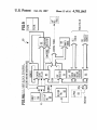
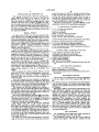
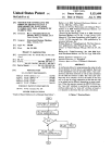
11 Claims, 19 Drawing Figures
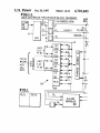
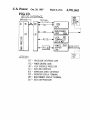
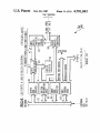
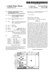
USER INTERFACE PROCESSOR BLOCK DIAGRAM.
,‘
mumssumn
6%“
2|
:2
s-
"°“‘
i2
vmumn
391.
CRIB-1
was
or: '61
~
:16
scc
was
Pccso-
A1110 CALL .
H8115
'
’
E!
' m
l’P‘tlS H °'°
Q
out!
3,.
t2
:2 I“
; WM
m
"
2'
4-’
" ----- ——<:m
/
*-'
E
PIT
E
m
g
PRWC
'
"'“I
n
‘L’
100
"T'
(m
2
Fr’
w
‘
tumor
WITMLER
@A-
M
'
H.
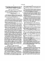
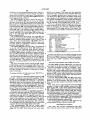
U. S. Patent Oct. 20,1987
Sheetl ofl6
4,701,845
FIG.1-1.
USER INTERFACE PROCESSOR BLOCK DIAGRAM.
5
.
CLEAR
'6\
[ HMADDRESS
LATCH)
PAL —->
2|)
Lzi
'
N0
I2
I2
N3
'6
MPU
CT L 8282'
u
'(HLDAI)
.
NN )
DATA Bus\
‘
*'
l6
SEC
LINES
7'
Pccso-
'6'
5
'
23g HUT
------h9g3“@ZA
<H Clo Ff”
8
Q
_
sec
MODEMS-J g; L'NES
u.’
8
E
' ' 2M
T"
5
CALL-
‘=5 FP#4 MC‘
2
UNITS
‘’ -------- "@wib-
;
PIT
;
—’
m
‘L
L4
L
/
100
8
PRITC
\ JFLN
l
T’
4s00
FIG-l.
2
+I
F|G.1-l.
FlG.1-2.
‘
2°)
'
,
,6 '
:1 E
DLI/HDP
_
,
CONTROLLER
5
’
M
US. Patent Oct. 20, 1987
Sheet3 of16
$25
F
.as
:A
1
22ww$2E:351:5s12w55525‘
w
52
:5;ENE?I 0m2:3ho,aI;i:€5£5%§:52;E:>5
5.4H8752U3mE%?52
4,701,845
253%;amo:so:1an
\m2
I
=2:. 0%:2
‘x
5:S2E5:8E23aas58
.8
3m
.320:55s
:2 5;:
5%
EQQ:.
g25I;92:5
U. S. Patent Oct. 20,1987
Sheet4 of 16
:22o:2: a:
l?s1:35o8l2:v;53
a
, .so:
a
021
+
s2:22‘25a?. .
so25aam,
a
A
:2:
w
SIE24 8
E8G04$3E2:an
E2m5%as5OE:
4,701,845
25;:
W05 ;
wasmm
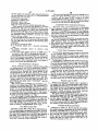
US. Patent Oct. 20,1987
,
‘
SheetS ofl6
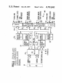
FIG.1C.
4,701,845
I
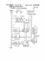
UIP AND SYSTEM MAINTENANCE INTERFACE.
32-»
I
>
'. MCI“
I
;M-BUS
SHIFT CHAIN
‘I 30m]
I
Q 'T-KIMhZCLII
E
~—sTRETcH cu<——
MAIN
PROCES R
DIAGNOSTIC
CONTROLS,
1—-—-
I
500
<———
1NTERRuPTs——> PIC '—DIAGNOSIICCONTROLS—> “DP
“DIAGNOSTIC CONTROL—>
4-SHIFT CHAINS_>
~-SHIFT CHAINS———>—
8 MhZ CLII__—->
BUS IOO\ I £IOOIJ
0m
REMOTE
DLI
IOOI
SUPPORILINII
‘HELP DLI/DLI
LEGEND:
UIP = USER INTERFACE PROCESSOR
PIC = PROCESSOR INTERFACE CARD
ODT = OPERATOR DISPLAY TERMINAL
DLI = DATA LINII INTERFACE
'
DLI/MLI = DATA LINK INTERFACE and/0T
MESSAGE LEVEL INTERFACE
MCU = MEMORY CONTROL UNIT
HDP = HOST DEPENDENT PORT
“I
II
U. S. Patent Oct 20,1987
Sheet8 ofl6
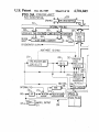
F1G_3A_ PRIOR ART
scc DATA PATHS.
-
4,701,845
>430
CPU M0 <::> M0 DATA BUFFER
[L
F
2|2\
_
INTERNAL DATA Bus
U
,
262x
4% T
UPPER BYTE TTNE CONSTANT LOWER BYTE TIME CONSTANT
_R_E_c_E_Ty_E_
DR|NpU'|'—->
GEN. A}l6 BU 264
7.
i}
DOWN : COUNTER
BATA
"m6"
266
7
—2
DR GENERATOR 0BTPBT+
r-JTQNIMQQLliLSXNQX ............ -
A
m1SYNC REGISTER
5 AND
——-
2B0P zazlg??gm
SBITS T—>REGISTER
ZERO DELETE
A
A
(8 BITS)
,I
*
t
SYNC
CRC
2B4L cRB DELAY
.
REGISTER
(BBITS)
+
INTERNAL TXD
j SOLO-2072“ 286 CRCRESULT
MUX
270‘\ 272 l 274_\
RXD
lBlT —T—>MUX
NRZIDECODE
{
DFLL—>
DFLL ->DFLL OUTPUT
x2“
9
200
A
CRC CHECKER
' ;
'FIG.3.
ETBBA, TTBBB.
U. S. Patent Oct. 20,1987
FIG-.33.PRICDR
Sheet 9 of 16
4,701,845
ART
212-2
"
TO OTHER
F
2546} 236\ {}238\Q}240\U
BEEN;
wRT SYNC
ERROR;
REGISTER REGlsTER OATA
“0 2349
{}
:>RECEIVE
E53,?
wRG SYNC
CHANNEL
TRANSMIT
{,L E i}
lNTTXEFéNAL
{} 246R A
2ORTT §SH|FT REGISTER ;sTART
REG'STJ-ERI
242
244
Q 288
3 f B”ETNAL'TX256)MUX —
A
A
T A
l
TRANSMTTL
MUX &
28H
l
NRZI ENGOOE
\
3
———> DELAY
254
INSERT
K (SBITS)
GRG
GENERATOR \
TRANsNTT CLOCK
250
AT
BR GENERATOR OUTPUT——>
DPLLOUTPUT
. ZQQ_>RECE|VE CLOCK
“
TR=C—————> 2 —->TRANsN|T GLOGN
RT=G
SYNC OSCILLATOR
z
g—->DPLL CLOCK
\.
g —>OR GENERATOR CLOCK
2OO
U. S. Patent Oct. 20,1987
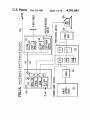
Sheet 12 of16 4,701,845
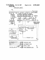
PORTC409
PIC-16w
(IO PORT c BLOCK DIAGRAM.
lNTBEggAL
SEEM-4
PORT
TOCOUNTER-TTMER3
PORT
( 403, FIG. 4 )
?
.
TO COUNTER/TIMERS
l
x
TO PORTT'T
TOPORTO
L6
"OJ-Q 1%“
HANDSHAKE AND
m
-
REQUEST / WAIT LOGIC
_
\,
6'“
IRRR
>8HUT
:>DATA
52L)
MULTIPLEXER
REOTsTER
ON‘EERTERS
1's
GAMER
6H\_
INPUT
(
DATA
PORT
I/O
/L
REOTsTER\
.
T
.
Om
(
ONTPOT
y--T,:>ONTTER/
PORT
>C0NTROL
LOG'C ‘
I
6|8,
INVERTERS
622
BIB
L+620,
INTERNAL PORT
CONTROL LINES
T
.
UQM
Sheet 13 0f16' 4,701,845
c
mL/\/,\
53851
5551.mg. ‘MAT
v
3525as;222$25:850,2: . X w2 5.:2255.2r3.2
5:Q;5M28:m52:8
_352s 53
N$56.U2:3Em8P5
WWW253 2O?z2aiuzé
@
2x
Eo:0
m2:
mmm5:52
‘ mékOEmaq
N3
UQM
vam.w55"$2.A52
mUENag;EPKPQ02mWE?
:5
n
m
.m
m
wlom
2+
o;AMV
55%mi+I02%a Wmqnum+0
m
Em
El
m
wmas,m
w
%
E
.v
m
kw
a
L
1:1._|l9\ \l\
Q13mwwsSw52E.28 ma‘
2:
N
N;1,
amn9%mismeimlsT
a2W7Em'<,1M8;wm27'52-I omOsNf
ZmIMHYAHK
d5
w.mmmmAwl5v2z:il5s2v.5
mmamm2?vETv%334,4Eu21mum5'225w
5m. AIV
mM1.M5$2915|2.‘5:
EmmwQAnI (
H20‘WNWI',m l
w
2?;.
1
4,701,845
2
mation, to external cabinets and to a power control card
which enables connection to a remote support center
USER INTERFACE PROCESSOR FOR COMPUTER
NETWORK WITH MAINTENANCE AND
PROGRAMMABLE INTERRUP’I‘ CAPABILITY
for comprehensive diagnostic and fault-location ser
vices.
The User Interface Processor connects to the central
host processing unit through a processor interface card
and to various peripherals and terminals through a data
FIELD OF THE INVENTION
This disclosure relates to the area of computer net
works and to specialized processors which operate a
link interface/host dependent port controller.
maintenance subsystem for the network.
A set of serial communication controllers and com
munication input/output units work together with a set
of timers and a priority interrupt controller in order to
communicate with the main host processor, both for
CROSS REFERENCES TO RELATED
APPLICATIONS
This application is related to a copending application
entitled “Maintenance Subsystem For Computer Net
work", U.S. Ser. No. 664,670, ?led Oct. 25, 1984, by
normal operational purposes and also for maintenance
and diagnostic services.
15
inventor David Andrew Andreasen, et a1.
BACKGROUND OF THE INVENTION
In the design and development of computer system
networks, there are many considerations and trade-offs
which must be balanced in order to provide an optimum
system and to decide what limits must be drawn in
terms of economic factors, size and space factors and
Each one of a series of local computer networks may
be locally checked on self-testing procedures and then
connected to a remote support center for comprehen
sive diagnostics in order to locate speci?c problems
within any given computer network system. Many dif
ferently located computer system networks may be
connected to one remote support center which can
service them all on a time shared basis.
versatility of control of the system.
BRIEF DESCRIPTION OF THE DRAWINGS
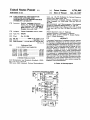
The presently described computer network system is 25 FIG. 1 is a block diagram of the User Interface Pro
designed not only to be used with a variety of periph
cessor used in the maintenance system network; FIG. I
eral type devices but also with data comm and tele
is made up of two sheets labeled FIG. 1-1 and FIG.
phone lines to remote terminals to provide rapid trans~
1-2;
ference of data between the units and rapid data pro
FIGS. 1A, 1B, 1C and ID are system and network
cessing by a central processing unit in a fashion 30 drawings showing how the User Interface Processor
whereby reliability is maintained to a very high degree.
module connects to other elements of the system net
The system is organized so that each of the various
work to provide a maintenance subsystem;
elements and units will, when initiated, provide its own
FIG. 2 is a block diagram of the serial communica
self-test routines and report the results and information
tions controller elements of the User Interface Proces
to a maintenance processor called the User Interface 35
sor;
Processor 100. This processor works in conjunction
FIG. 3 is a block diagram showing the data paths
with the various remote terminals, and the various types
involved in the serial communications controller; FIG.
of peripheral devices through an I/O subsystem which
3 is made up of two sheets designated as FIG. 3A and
is uniquely designed to handle units called "data link
processors”. These types of data link processing units 40 FIG. 3B;
FIG. 4 is a block diagram of the communications
were described in their earlier versions in U.S. Pat. Nos.
input/output unit elements of the User Interface Pro
4,415,986; 4,392,207; 4,313,162; 4,390,964 and 4,386,415.
cessor;
The maintenance subsystem involved herein is so
FIG. 5 is a block diagram showing the ports of the
interconnected to the various elements of the system
that self-test data may be collected and transported to a 45 communication input/output unit;
FIG. 6 is a block diagram of the communications
remote diagnostic unit which may be a central diagnos
input/output port designated as port C;
tic unit for many, many computer networks in many
FIG. 7 is a block diagram of the counter timers of the
different locations. The remote terminal will perform
communications input7output unit of FIG. 4;
the basic diagnostic routines to any of the computer
FIG. 8 is a block diagram of the priority interrupt
networks which have problems and will send messages 50
controller (PRITC) of the User Interface Processor;
which pinpoint the speci?c cause or location of the
FIG. 9 is a block diagram of the unit designated as the
trouble so that a local operator may correct the fault by
data link interface/host dependent port. FIG. 9 is made
changing a card, replacing a module or ?xing any other
up of two sheet labeled 9A and 98;
designated fault or outness.
55
SUMMARY OF THE INVENTION
The User Interface Processor of the present disclo
sure is a specialized processor known as a maintenance
processor which supports a computer system network
which involves a central processing unit connected to
many remote peripherals through data link processors
and other remote terminals via telephone lines.
GENERAL OVERVIEW
The Maintenance Subsystem
The maintenance subsystem of the computer network
is organized around the User Interface Processor 100
which is shown in FIGS. 1A, 1B, 1C and 1D.
As seen in these drawings, the User Interface Proces
sor is connected to all the various elements of the com
The User Interface Processor or "maintenance pro
puter system network, that is to say, it connects to the
cessor" provides an interface to the central host pro
processor interface card and the main host processor on
cessing unit and to various elements of the network 65 the one hand and, on the other hand, it connects to the
such as the data link processors which connect to re
power control card, the maintenance card III, the oper
mote peripherals, to the operator display terminal
ator display terminals and the various data link proqes
which provides visual information and diagnostic infor
sors.
3
4,701,845
4
provide automatic power ON/OFF operation; to pro
Thus, these combinations of elements connected to
the User Interface Processor I00 provide the basic op
erational and maintenance functions for the computer
network. For example. the User Interface Processor 100
will initialize and power up the entire computer net
work system. It will initiate self-testing procedures,
whereby each of the interconnected data link proces
vide “remote" power control of external cabinets; to
maintain an internal time-of-day clock; and to provide a
communication path (data link) for a remote support
and diagnostic service.
The processor interface card 40 (FIG. 1A) functions
to provide control and data acquisition for diagnostic
testing of memory 34 (FIG. 1B), memory control unit
32, host dependent port 500 and the main processor 30;
sors will do their own self-test, do a check out routine
and send the results back to the User Interface Proces
sor. Additionally, the User Interface Processor will 0 the PIC 40 provides initialization functions such as
microcode load, initialization state and clock control.
connect to the power control card in order to provide
and distribution. The PIC 40 provides a history file,
maintenance and diagnostic information and data to a
FIG. 1A, for real-time tracing of microcode addresses
remote unit which can then provide further diagnostics
which will determine the location of any faulty areas in
(break points); it provides 16 general purpose links for
tracing of intermittent failures, and it permits perfor
the system.
Further, the User Interface Processor will initiate its
"own self-testing“ routines to make sure that it itself is
mance‘monitoring so that a trap can be set to count the
in proper operating condition and it will display the
communication path (AULF register, CSCP operator)
number of failure occurrences. The PIC 40 supplies a
so that the main system processor 30 can communicate
results on the operator display terminal.
Processor Interface Card (PIC)
The processor interface card 40, FIGS. 1A, 1C, in the
maintenance subsystem is used to provide the basic
system clocks. and in addition it provides data link inter
face input/output clocks of 8 megahertz. It provides an
interface to the processor backplane and also provides a
unit called the system event analyzer, 408. Further, the
PIC provides 4,000 l6-bit words of history trace 40;, in
order to maintain a history of any selected input signal.
Additionally, it provides a 16 K byte memory which
20 to the UIP 100 for maintenance information on power
holds the error correction bits for the control store in
the User Interface Processor.
The Power Control Card (FCC)
The power control card 50, FIG. IA, will control the
power on/off sequencing and detect any DC failures for
all power supply modules which are connected directly
to the PCC.
The PCC also monitors any air loss and cabinet over
off, time of day, reload, etc.
In FIG. 1B the memory bus 30,,1 connects the main
processor 30 to the memory control unit (MCU) 32 and
to the UIP 100.
Also attached to memory bus 30," is the host depen
dent port 500 (HDP) which provides a DLI (data link
interface) bus 54 to the I/O subsystem 500,, and a mes
sage level interface (MLI) bus 5," to the I/O expansion
module 500‘. which connects to peripheral devices.
FIG. 1C shows, in greater detail, the UIP 100 con
nections to the HDP 500 and to the processor interface
card (PIC) 40 which interconnect the main processor 30
and the I-IDP 500.
FIG. 1D shows how the UIP 100 connects to the
processor interface card 40 and main processor 30 on
one side, and to the I/O data link processor 100;, to
maintenance card 100,", and to ODT 100, and remote
link 50,”. The acronym ODT refers to “operator dis
play terminal”.
The User Interface Processor 100, FIG. 1, is desig
temperature in order to provide sensing signals to this 40
nated with the acronym “UIP”. The User Interface
effect.
Processor consists of one logic board which can inter
The power control card communicates with the User
face to a data link interface (DLI) backplane and also to
Interface Processor via an 8-bit parallel bus. It further
four independent serial data communications interfaces.
communicates with any remote device using the RS
Under certain software instructions, the User Inter
232C remote link interface. It can communicate with 45
face Processor 100 can operate as a data link processor
other power control cards on external basis by using
(DLP) and in so doing will support a burst rate of up to
two wire RS-422 direct connect data communication
eight megabytes per second. It can also be used as a host
protocol.
dependent port (HDP) where it will support a burst rate
The power control card 50 also maintains a battery
of 50 kilobytes per second. Thus, the same card of hard
backup with the time of day function, in addition to
providing 256 bytes of non-volatile storage memory. It
ware can be made to assume different personalities and
also provides an automatic restart option after failure of
the AC power lines.
functions as required.
DESCRIPTION OF PREFERRED EMBODIMENT
The User Interface Processor 100 operates on a main
tenance philosophy whereby cards in a computer sys
tem as FIG. 1A can be isolated and replaced. A combi
FIG. 1A shows the User Interface Processor 100 as
nation of "self test" and “peripheral test-driver" tests
part of a network con?guration. The output bus 100;, of
microprocessor 110 connects to the processor interface
(PTD) are used to isolate any failure to a replaceable
card 40 and to the memory bus 30", which connects the
main processor 30, FIG. 18, to the memory control unit
32 and main memory 34.
In FIG. 1A the DRAM 150 provides output to the
power control card 50 and the erasable PROMs 150
module. This is done by indicating to the operator (via
operator display terminal, ODT, 100,) the identity of a
failing board after the completion of the self-test.
Thus, the User Interface Processor 100 is basically a
microcomputer system which is placed on a single
printed circuit board. It includes a number of key com
ponents as follows:
connect to the operator display terminal 100,.
(a) a 16 bit central processing unit 110, FIG. 1;
The power control card 50 (FIG. 1A) functions to 65
(b) 192 kilobytes of PROM, 1700,’, (FIG. 1);
provide power up-down sequencing; to monitor for
(c) up to one-half megabytes of RAM, 150a‘;J of FIG.
power failure, to initiate automatic restart (after power
failure); to provide warning of over-temperature; to
1;
S
4,701,845
(d) programmable input-output ports (2020, 202),);
6
(ii) a dynamic RAM of 512K bytes (150“);
(iii) a PROM of 192K bytes (EPROM) 170;
(iv) four serial data communication ports (200”,
(e) serial data communication ports (200”, 200),);
(f) a priority interrupt controller, (PRITC 800);
(g) programmable timers, (PIT 700);
2020.0);
(h) a DLI-HDP controller 180 (DLI=Data Link
(v) six parallel I/O ports (two units of 407, 408, 409);
(vi) programmable interval timers (PIT 700);
(vii) a programmable interrupt controller (PRITC
Interface);
(i) a DLI host dependent port (I-IDP), 500 of
FIG. 1B.
The User Interface Processor 100 can communicate
800).
These elements are shown in FIG. 1 of the drawings.
via the controller 180 and through the U10 (universal 10
input output) backplane to a host computer using a
standard UIO-DLI backplane protocol which conforms
to the Burroughs Message Level Interface as described
in U.S. Pat. No. 4,074,352 at FIG. 515, this patent being
MICROPROCESSOR 110
The microprocessor 110 is used to drive the User
Interface Processor 100 and may constitute an eight
megahertz chip designated as the INTEL 8086-2
(iAPX-86/10). This microprocessor chip is described at
entitled Modular Block Unit for Input-Output Subsys
tern.
pages 3-1 through 3-24 in an INTEL publication enti
tled Microprocessor and Peripheral Handbook - 1983
The User Interface Processor is capable of simulating
a DLI host dependent port, thus enabling it to commu
(Order No. 210844-001) and published by INTEL Lit
nicate with data link processors in a common base that
erature Dept., 3065 Bowers Avenue, Santa Clara, Ca.
does not have a "distribution card". It emulates the 20 95051.
priorly used Distribution Card. The description of data
This processor is a high performance 16-bit CPU
link processors and use of the “distribution card” have
which is implemented in HMOS technology and pack
been described in U.S. Pat. Nos. 4,313,162 entitled I/O
aged in a 40 pin dual in-Iine package. This processor is
capable of addressing up to one megabyte of memory,
Subsystem Using Data Link Processors, and 4,390,964
entitled Input/Output Subsystem Using Card-Reader
Peripheral Controller.
25 as well as 64k of I/O addresses. The 8086 microproces
,
sor is operated in a minimum mode since it is used only
in a single-processor environment, and as such it gener
ates its own bus control signals.
The User Interface Processor includes a backplane
interface to a bus known as the backplane maintenance
' bus. These backplane lines can be used to initiate a data
link processor self-test routine and to read a result of 30
that self-test as it is driven on to the backplane from a
given data link processor.
In this disclosure, the two above-mentioned user
interface processor ports will be referred to as the DLP
and the HDP respectively.
The User Interface Processor 100, FIG. 1, is a micro
processor controlled system that contains:
(i) a microcomputer subsystem (110);
(ii) a data link interface controller (180);
(iii) a host dependent port controller (180);
These three units allow the User Interface Processor
to communicate with the host computer (30, 32, 34),
FIG. 1B, via the DLI controller 180 (FIG. I) and also
DYNAMIC RAM 150
The microprocessor 110 is provided with access to a
dynamic RAM array of 128 bytes. The array 150 of
FIG. 1-2 is organized as 64x18 bits and it is byte
addressable by the microprocessor 110. The RAM
35 array 150 is controlled by a dynamic RAM controller
chip, of which the preferred element is the National DP
8409. This chip is described at pages 350-391 in a publi
cation entitled NS 16000 Data Book, 1983, and pub
lished by the National Semiconductor Corp., 2900
Semiconductor Drive, Santa Clara, Ca. 95051.
This chip provides all the necessary multiplexing of
the row and column addresses, drivers, and the refresh
logic. Since this chip is operated in its fastest mode,
with other data link processors 1004, FIG. 1D, that are
there is no wait state required. A “refresh request" is
connected to the I/O backplane, via the host dependent 45 requested every 1.6 microseconds by a refresh counter
port 500 of FIG. 1B.
which, in turn, requests a 8086 hold sequence (in micro
The UIP 100 has certain communication restrictions
processor 110) to occur. Once the sequence is granted,
in this regard. The host dependent port 5110 is a DLI
the RAM controller chip (DP 8409) accesses one row
(Data Link Interface) controller (180) and as such does
of RAM 150, thus refreshing it.
not provide a MLI (Message Level Interface), but
The duration of this access equals that of a micro
merely provides a backplane DLI interface. In this
regard it cannot be used with a distribution card, path
processor memory access cycle, thereby reducing the
refresh overhead time to a minimum. With this type of
selection module, or base control card as was done in
con?guration, the memory band width is 3.83 mega
the organization of data link processors which were
bytes per second. The memory is refreshed also during
described in the cited U.S. Pat. Nos. 4,313,162 and 55 a “reset" of the microprocessor 110, thus preventing
4,390,964, since it provides these functions for itself in
destruction of the memory contents.
?rmware. This particular host dependent port 180,
Error detection in the RAM array 150 is accom
FIG. 1, must be used in a base that provides an eight
plished by vertical byte parity via circuit 160, FIG. 1-2.
megahertz clock, such as that provided from the main
Thus, each 16-bit word of RAM 150 has two parity bits,
tenance card, 100," of FIG. 1D.
60 one for each byte. Whenever a word, or a byte, of a
MICROPROCESSOR SUBSYSTEM
The microcomputer subsystem includes both serial
and parallel interfaces that are used to perform data
communication operations.
The microprocessor subsystem consists of certain
elements as follows:
(i) a microprocessor 110 (such as Intel 8086);
dynamic RAM is accessed, the parity is checked for
each byte regardless of whether the operation is a word
cycle or a byte-memory cycle. When such an error
occurs, the microprocessor 110 has its non-maskable
65 interrupt set to “true“, and the error logging can then be
implemented to record the bad address (when such an
implementation has been provided in the UIP 100 firm
ware).