1
Computers and Microprocessors
1-1
Introduction
Over the last few decades, computers, and microprocessors in particular, have
begun to have an enormous impact upon our lives. In early stages of development,
computers were expensive, large, slow, centralized machines, consuming large amounts
of electrical power. All this has changed fundamentally as microelectronics has reduced
the cost of computing power and increased the data processing capabilities of a silicon
chip. The development of the microcomputer (one or more integrated circuit chips
that provide all the functions of a computer) is revolutionizing the computer industry
and many other industries as well. Because of their low cost, small size and versatility,
microcomputers made available cheap and virtually unlimited computing power.
A microcomputer system is generally built around a microprocessor. The
microprocessor chip contains within it most of the control, logic and arithmetic functions
of a computer. To become a complete microcomputer, other integrated circuit (IC)
chips, such as RAMs (Random Access Memories), ROMs (Read Only Memories) and
peripheral devices for input/output have to be added.
The first practical IC microprocessor, the Intel 4004 appeared in 1971. The 4004
was a slow, 4-bit CPU holding about a few thousand PMOS transistors. Intel rapidly
followed up with microprocessors of greater complexity: the 4040, the 8008 and the
8080 series. Other manufacturers responded rapidly with effective, if not better micro
families; 6800 series from Motorola, 6500 from Rockwell and Z80 from Zilog.
The fast evolution of microelectronics resulted in ever growing chip density.
Smaller transistor structures increased overall switching speed, decreased power
consumption, and allowed designers to integrate more transistors on the same area.
More transistors allowed higher complexity functions to be realized on a single chip of
silicon. Today, besides a wide palette of 8-bit microprocessors, 16-, 32- and 64-bit
microprocessors have become available to the design engineer. Not only the integration
density, but also the throughput has increased considerably from a few ten thousand
instructions/second to over billion instructions/second for the most advanced
microprocessors used in personel computers and workstations.
The evolution of the microprocessor not only enabled us to build and use powerful
computers, but also allowed us to control a vast variety of equipment. Integrating
CPU core, RAM, ROM and I/O on a single chip a complete smal scale microcomputer
was obtained. Single chip microcomputers are used, where the device is dedicated to
a specific operation, space is limited, and large volume production is the case.Since
most of these microcomputers were used to control some equipment, they were called
microcontollers. The first 8-bit microcontroller, the F8, was introduced by Fairchild in
1974. The ever growing demand for embedded control resulted in development of
powerful microcontrollers. General Motors was the first company to use a
microcontroller in its high-end cars. This microcontroller was the Motorola MC6801
1
with an enhanced 8-bit CPU, 128 bytes of RAM, 2 KBytes of ROM, 31 parallel I/O
lines, an asynchronous serial communication interface, and a 16-bit programmable
timer. Today a typical car uses more than ten microcontrollers.
Development in VLSI and electronic CAD technology enables us to rapidly design
and produce sophisticated microcontrollers tailored for specific applications. Still the
majority of microcontrollers are 8-bit devices, but these devices now make use of flash
memory technology to replace ROMs and EPROMs. Flash memory for program and
system parameter storage enables the equipment manufacturer to easily update software
and system parameters without removing the chip from its circuit, thus reducing
service cost and time.
This book will be based upon the Motorola HC08 family of microcontrollers with
special emphasis on the MC68HC908GP32. This device has an 8-bit CPU core, 512
bytes of RAM, 32 kilobytes of flash memory, parallel and serial I/O, multifunction
timers, and A/D converter.
1-2
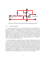
Basic Computer Structure
A computer, and a microcomputer in particular, can be defined as a machine
which manipulates data according to a stored program executed within it. The data is
often thought of as numbers, but can, with suitable processing, be any physical parameter
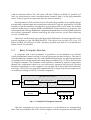
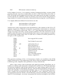
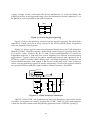
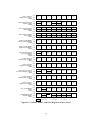
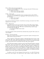
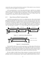
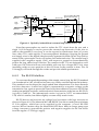
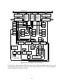
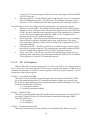
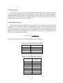
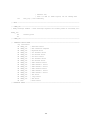
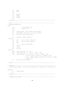
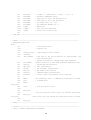
or quantity which can be represented using binary numbers. Fig. 1.1 shows the structure
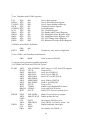
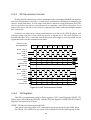
of a simple computer. The computer can be split into a number of separate components,
though the components shown do not necessarily represent the physical division
between components in a real computer. For example, the Control Unit and Arithmetic
and Logic Unit (ALU) are generally implemented as a single chip, the microprocessor
or central processing unit (CPU), in microcomputers.
(Microprocessor or CPU)
Clock
Controller
Data & Instruction
RAM/ROM
Memory
Data Operator (ALU)
Input/Output Units
Fig. 1-1. Simplified Computer Structure
The first requirement of any microprocessor is a mechanism for manipulating
data. This is provided by the ALU of the computer, which can perform such functions
2
as adding or subtracting two numbers, performing logical operations like AND, OR,
NOT, and shift and rotate operations. More complex ALUs can perform additional
more powerful instructions like multiply and divide. From this very basic set of
operations, more complex processing functions can be generated by programming.
Clearly, every computer must include a mechanism to communicate with the
outside world. All communication will be done via an input and an output unit. The
outside world may consist of someone typing at a keyboard of a computer terminal
and watching the response on a screen, or it may be some equipment, for example an
air conditioning system, which is proving data inputs such as temperature and relative
humidity of the interior and outside, and is being controlled according to the program
inside the computer, via computer outputs which switch on and off heater or cooler,
moisturizer, fan etc.
The computer must include memory which serves two functions. First, it provides
storage for the computer program and data (main memory); second it provides
temporary storage for data which may be used or generated at some point during
program execution by the ALU (registers). Main memory is organized as a onedimensional array of words, and each instruction or data variable occupies one or
more words in memory. Each word is made up of a number of bits (binary digits) of
storage in parallel. The number of bits in each word is defined by the designer of the
computer or microprocessor, and is one measure of the computer's processing power.
Most microprocessors have word lengths of 8 bits (byte), 16 bits (word) and 32 bits
(long word).
The control unit of the microprocessor controls the sequence of operations of all
the components described above, according to the instructions in the computer program.
The control unit is responsible for execution of all sequential operation steps of an
instruction. First instruction is fetched from memory (called instruction fetch), then
decoded by the control unit and converted into a set of lower level control signals
which cause the functions specified by that instruction to be executed in sequence.
After the completion of execution of the current instruction the next instruction is
fetched and the above process is repeated. This process is repeated for every instruction
except for so called program flow control instructions, like branch, jump or exception
instructions. In this case the next instruction to be fetched from memory is taken from
the part of memory specified by the instruction, rather than being the next instruction
in sequence. All operations in the control unit are synchronized to a fixed frequency
clock signal to ensure all operations occur at the correct time instance. This clock
signal is either an externally applied signal input, or it is generated internally from a
crystal connected to the microprocessor. The clock frequency defines the instruction
execution speed of the microprocessor and is constrained by the operating speed of
the semiconductor circuits which make up the computer.
The patient reader has recognized the fact that memory contains both instruction
and data, and furthermore, both flow from memory to microprocessor and vice versa
via the same common way. How can the microprocessor distinguish between instruction
and data, and why do we not use different memories for instruction and data? Using
just one memory for both instruction and data simplifies the hardware and reduces
3
overall cost. This architecture is called the von Neuman architecture, named after the
scientific giant of our century who invented it. The microprocessor cannot distinguish
between instruction and data, therefore the programmer is responsible for correct
program flow.
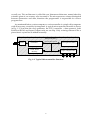
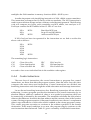
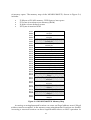
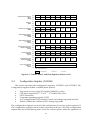
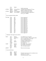
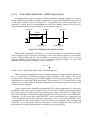
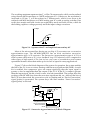
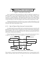
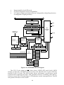
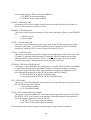
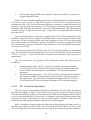
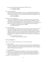
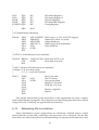
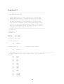
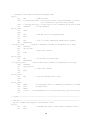
As mentioned before a microcomputer or microcontroller is a single-chip computer
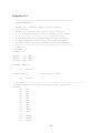
with all necessary circuit blocks integrated. A typical microcontroller structure is shown
in Fig. 1.2. Note that the clock generator, the CPU (controller + data operator), both
RAM and ROM, and Input/Output units are on-chip. Only a timing reference like a
piezoelectric crystal has to added externally.
(Microcontroller)
Clock
Controller
Data & Instruction
RAM/ROM
Memory
Data Operator (ALU)
Input/Output Units
Fig. 1-2. Typical Microcontroller Structure
4
Instructions and Addressing Modes
2-1
The Programming Model
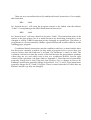
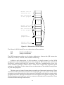
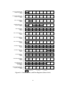
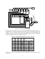
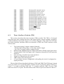
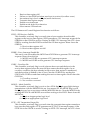
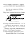
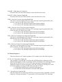
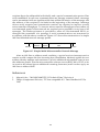
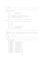
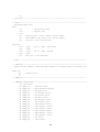
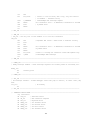
Before going into detail of instructions and addressing modes let us examine the
programming model of the HC08 family of processors. The HC08 family are 8-bit
microprocessors with some 16-bit extensions. The registers inside the HC08 accessible
to the programmer are shown in Figure 2-1, where the longer registers hold 16 bits
and the shorter ones hold 8 bits [1]. Let us have a brief description of all these
registers.
7
0
Accumulator (A)
A
7
15
H
0
X
15
Index Register (H:X)
0
Stack Pointer (SP)
SP
15
0
Program Counter (PC)
PC
V 1 1 H I N ZC
Condition Code Register (CCR)
Carry/Borrow Flag
Zero Flag
Negative Flag
Interrupt Mask
Half Carry Flag (From Bit 3)
Two's Complement Overflow Flag
Figure 2-1. Programming Model of the HC08 family
Accumulator
The accumulator (A) shown in Figure 2-1 is a general-purpose 8-bit register. The
central processor unit (CPU) uses the accumulator to hold operands and results of
arithmetic and non-arithmetic operations.
Index Register
The 16-bit index register allows indexed addressing of a 64 KByte memory space.
It is formed by concatenating the H and X halves. The predecessor of the HC08 family,
the HC05, owned only an 8-bit index register X. To guarantee object code level
compatibility, this architecture has been adopted and hardware reset clears the high
portion (H) of the index register (H:X).
5
Stack Pointer
The stack pointer (SP) is a 16-bit register that contains the address of the next
location on the stack. Stack is an area in memory reserved for sequential storage and
retrieval of temporary data. Temporary data can be saved by pushing data bytes onto
stack. Here the stack pointer serves as an automatic address generator by decrementing
itself after each push (save on stack) operation, to point to a new unused location. The
read from stack or pull data operation is performed again by the assistance of the
stack pointer. To pull a byte from stack, first the value of the stack pointer is incremented
by one to point to the data to be pulled, then the actual read memory operation is
done.
For a large number of instructions the stack pointer can also be used in the same
way as the index register enabling the programmer to use so called stack pointer
indexed addressing.
As in the case of the index register H:X, the stack pointer is preset to $00FF during
a hardware reset for HC05 family compatibility. Note that execution of the reset stack
pointer (RSP) instruction presets the least significant byte to $FF, but does not affect
the most significant byte.
Program Counter
The program counter (PC) is a 16-bit register that contains the address of the next
instruction or operand to fetched. Normally, the program counter automatically
increments to the next sequential memory location every time an instruction or operand
is fetched. Instructions like jump, branch, subroutine call, and interrupt operations
load the program counter with an address other than that of the next sequential
location. During reset, the program counter is loaded with the reset vector address
contained in locations $FFFE and $FFFF. The vector address is the address of the first
instruction to be executed after exiting the reset state.
Condition Code Register
The 8-bit condition code register (CCR) contains the interrupt mask and five flags
that indicate the result of the instruction just executed. Bits 6 and 5 are unused and set
permanently to logic 1. Let us briefly describe the use of these flag bits:
V - Overflow Flag
This bit is set whenever a two’s complement overflow occurs as a result of an
operation. The V flag is important for signed arithmetic operations.
H - Half-Carry Flag
The CPU sets the half-carry flag when a carry occurs between bits 3 and 4 of the
accumulator during an add-without-carry (ADD) or add-with-carry (ADC) operation.
6
The half-carry flag is required for binary-coded decimal (BCD) arithmetic operations.
The decimal adjust accumulator (DAA) instruction uses the state of the H and C flags
to determine the appropriate correction factor.
I - Interrupt Mask
When the interrupt mask is set, all interrupts are disabled. Interrupts are enabled
when the interrupt mask is cleared. When an interrupt occurs, the interrupt mask is
automatically set after the CPU registers are saved on the stack, but before the interrupt
vector is fetched.
N - Negative Flag
The CPU sets the negative flag when an arithmetic operation, logical operation, or
data manipulation produces a negative result.
C - Carry/Borrow Flag
The CPU sets the carry/borrow flag when an addition operation produces a carry
out of bit 7 of the accumulator or when a subtraction operation requires a borrow.
Some logical operations and data manipulation instructions also clear or set the
carry/borrow flag (as in bit test and branch instructions and shifts and rotates).
Details of flag use will be covered in the next sections along programming examples.
2-2
The Instruction
We now examine the notion of an instruction, one of operations performed by the
CPU. It can be described statically as a collection of bits in memory, or as a line of a
program or, dynamically, as a sequence of actions by the controller. The specification
of what the control unit is to do is contained in a program, a sequence of instructions
stored, for the most part, in consecutive locations of memory. To execute the program,
the CPU controller repeatedly executes the instruction cycle (or fetch/decode/execute
cycle):
1.
2.
3.
Read the next instruction from memory.
Decode the read instruction.
Execute the instruction decoded.
As we shall see with the HC08 family of microcontrollers, reading an instruction
from memory will require that one or more bytes have to be read. To execute the
instruction, some additional bytes might be read or written. The instruction read cycle
is usually called fetch cycle. The fetch cycle might be composed of multiple read
cycles. The first byte read from memory is called the opcode (operation code), decoding
this opcode the controller will decide whether to read more bytes or not to execute the
instruction. If besides the opcode byte or bytes, there are more bytes in the instruction,
those make up the data, called the operand. Whether an instruction is made up of a
7
single or multiple bytes is a function of the so called addressing mode involved.
We now look at the instruction statically as one or more bytes in memory or as a
line of a program. Each instruction in a microcomputer carries out an operation. The
types of operations provided by a von Neuman computer can be summarized as
follows:
1.
2.
3.
4.
5.
Move.
Arithmetic.
Logical.
Control.
Input/Output instructions.
We will examine these in detail later. Let us now examine how these instructions are
stored in memory as part of a program and how they are executed by the HC08. As an
example let us use the load instruction belonging to the move class of instructions. It
will move a byte from memory to a register. Depending on the register size one or two
bytes have to be transferred from memory to register.
If we wish to put a specific number, say hexadecimal 3F, into the accumulator, the
instruction would be written as
LDA
#$3F
where the symbol “#” denotes immediate addressing and “$” is used to indicate that
the number which follows is in hexadecimal format. If we had to put a specific number,
say $1240, into the index register (H:X), the instruction would be written as
LDHX
#$E240
Examining memory where the instructions are stored, we would see for
LDA #$3F
$A6
address n
$3F
address n+1
$45
address n
$E2
address n+1
$40
address n+2
and for LDHX #$E240
See that in machine code LDA has been replaced by $A6 and LDHX by $45 as a
result of the immediate addressing mode. Note that the 16-bit hexadecimal value
$E240 to be loaded into the accumulator is stored in the 8-bit wide memory as two
8
consecutive bytes, high byte first. Storing multibyte data in byte-wide memory high
byte at lowest and low byte at highest address is called big-endian format. All Motorola
miroprocessors make use of the big-endian format. In the drawing above, and all like
it that follow, the lower-numbered address will be towards the top of the drawing.
2-3
Addressing Modes
An instruction is made up of an operation code (opcode, for short) and of optional
input data (operand). The data will specify a source or destination address or an
immediate source value. The HC08 family, like most microprocessors, is a one-address
computer, because each instruction can specify at most one effective address in memory.
For instance, if an instruction were to move a byte from location 1000 in memory into
the accumulator, then 1000 is the effective address. This effective address is generally
determined by some bits in the opcode. The addressing mode specifies how the effective
address is to be determined, and is generally determined by some bits in the opcode.
If necessary, there are binary numbers in the data or operand field of the instruction
that are used to determine the address. The HC08 makes use of 6 different basic
addressing modes
1)
2)
3)
4)
5)
6)
Inherent
Immediate
Extended
Direct
Indexed
Relative
which will be discussed in detail in the next sections.
Inherent addressing
Source and destination of some instructions may be specified inherently by the
opcode itself. For instance, in the instruction CLRA, clear accumulator, source data for
operation is known, and the result destination is specified as accumulator. In this type
of addressing all instructions are of one-byte type.
Immediate addressing
As introduced in Chapter 2-1, the immediate mode is the simplest addressing
mode, where the value of the operand is part of the instruction. The adjective immediate
is used since the value follows immediately the opcode. This type of addressing is
used to initialize with constants or to provide constants for other instructions, such as
LDA, load to accumulator. Depending on the associated register size the immediate
data will be either 8-bits (byte) or 16-bits (word). For an 8-bit microprocessor 16-bit
data has to be stored in two consecutive memory locations. Note that with Motorola,
the description of a 16-bit data is always higher-order byte first; that is, the higher-order
9
byte has the lower-numbered memory location. The immediate mode of addressing
can only be used to load a register from memory.
Extended addressing
Since the program counter of the HC08 is a 16-bit register, a total of 216 = 65536
memory locations can be addressed. In the extended mode, a full 16-bit (two-byte)
description is used to specify the effective address of the data, even though the first
byte may consist of all zeros. As mentioned above, the higher-ordered byte is at the
lower-numbered memory location. If we wish to put the data contained at address
$0180 into the accumulator , the instruction would be written as
LDA
$0180
Examining memory where the instructions are stored, we would see for LDA $0180
$C6
address n
$01
address n+1
$80
address n+2
This instruction when executed by the CPU will access the memory cell at address
$0180, read its content and place it into the accumulator.
Direct addressing
Experience has shown that most of the accesses to data are to a rather small
number of highly used data words clustered together in a small memory region. To
improve both static and dynamic efficiency, the HC08 has a compact and fast version
of addressing, called direct addressing. In this mode the effective addresses high byte
is assumed to be equal to zero, and the lower byte is the only given part. This addressing
mode is also called zero-page addressing, because it restricts the memory addressing
range to the first (lowest) 256 locations. If we again wish to put the data contained at
address $0080 into the accumulator, the instruction would be written as
LDA
$80
Examining memory where the instructions are stored, we would see for LDA $80
$B6
address n
$80
address n+1
10
Comparing this example with the one in extended addressing, we immediately see
that direct addressing uses one less byte for the same operation. Reading only two
bytes from memory instead of three saves one byte in program memory and also
increases the speed of execution by one clock cycle.
Indexed addressing
Computer designers realized that, as good as extended addressing is, it is not particularly
efficient because it takes a couple of recall cycles to get the address of operand or
result from memory. To improve efficiency, the controller could be provided with few
registers that could be indirectly addressed to get the data. Such registers are called
pointer or index registers. Indirectly addressing through a pointer or index register
would be faster since less number of bytes are needed to specify the full 16-bit address.
Moreover, it has turned out to be the most efficient mode to handle many data structures,
such as character strings, vectors, look-up tables, and many others.
The HC08 got two pointer registers, called H:X and SP respectively. The H:X
register is the so called index register, whereas SP is the stack pointer. The index
register is used for indexed addressing, whereas the stack pointer is primarily used to
create a so called push-down pop-up stack. There are five different ways of indexed
addressing. The first three are the basic ones used to manipulate data structures like
strings, vectors, look-up tables, etc. To access a block of data in memory the index
register has to contain the base address or starting address of the block. The effective
address of the operand or result is the sum of the contents of the index register H:X
and a so called offset specified along with the instruction. This offset can be zero, a
one byte unsigned displacement between $00 and $FF, or a two byte unsigned
displacement between $0000 and $FFFF. For example, if we want to load into
accumulator the nth element of a look-up table starting at address $E400, then the
instruction would look like
LDA
$E400,X
Before executing this instruction, the index register has to contain n. The effective
address for the 16-bit offset case is calculated as follows:
Index Register (H:X)
16-bit unsigned offset
+
16-bit effective address
For the 8-bit unsigned offset case before the addition a zero is appended in front of the
offset to make it also a 16-bit positive number.
11
Index Register (H:X)
$00
8-bit offset
+
16-bit effective address
In the case of zero offset no addition is performed an the index register content is the
effective address. Use of no offset executes fastest with also minimum code, but can be
restricted in certain cases. Use of 16-bit offset executes slowest with also maximum
code size, but has no restrictions at all. Also note that in none of the cases the content
of the index register is modified.
In addition to the index register H:X, the stack pointer SP can also be used as an
index register with one or two bytes of unsigned offsets. This capability eases operation
on data pushed onto stack by a significant amount.
Stack Pointer SP
Stack Pointer SP
$00
8-bit offset
+
16-bit unsigned offset
16-bit effective address
+
16-bit effective address
An example for a stack pointer indexed addressing mode could be written as:
LDA
2,S
The fourth and fifth modes of indexed addressing are the “Indexed with Post
Increment, and Indexed”, “8-Bit Offset with Post Increment”. These are used only by
the CBEQ Compare and Branch if EQual instruction, and the MOV Move instruction.
In this addressing modes the index register H:X is used to address the operand either
using no offset or a one byte offset. After the operation on the operand the index
register H:X is incremented by one automatically. This special but powerful case will
be explained later in greater detail.
Relative addressing
The microcontroller is very much like any other computer; however, the use of
ROMs in microcomputers raises an interesting problem that is met by the last mode of
addressing. Suppose that someone buys a piece of machine code written for the same
family processor, but the machine code has to reside at an address not supported by
the microcontroller to be used. Since the programs source code is not available the end
user cannot modify or relocate the object code. If this specific program however had
been written in such a way that it does not make use of absolute addresses but only
relative ones, the complete code can be copied to any location to run. Such code is
called position independent. Program counter relative addressing, or simply relative
12
addressing enables us to write position independent software.
Program counter relative addressing, or simply relative addressing, adds a two's
complement number, called an offset, to the value of the program counter to get the
effective address of the operand. The 8-bit two’s complement notation offset is first
sign extended to form a 16-bit two’s complement number and then added to the
program counter as shown below:
Program Counter (PC)
sign extention signed offset
+
Program Counter (PC)
In the HC08, relative addressing is limited to conditional or unconditional branches
and to subroutine call instructions. A major drawback of the HC08 is the lack of the
relative addressing mode for load type instructions.
A simple program segment generating a small delay proportional to the contents
of accumulator can be written using a conditional branch instruction.
Loop
LDA
DECA
BNE
#$10
Loop
In this few lines of program, “DECA” decrements the contents of accumulator by one,
“BNE label” tests whether the result of the previous instruction (decrementation of
accumulator) was not equal to zero, and branches to the label “Loop” if so. It is
obvious that the program will loop 16 times, since accumulator had been initialized to
$10 = 16. Examining memory where the instructions are stored, we would see
$8021
$A6
LDAA #$10
$10
$8023
DECA
$4A
$26
BNE label "Loop"
$FD
$8026
Next instruction
where $26 represents the machine code for “BNE” Branch Not Equal instruction and
$FD or minus three decimal ($8023 - $8026 = -3) is the branch offset or displacement.
The BNE instruction updates the program counter such that it points to the “DECA”
13
DECrement Accumulator instruction at location $8023 or label Loop, if the zero flag Z
in the condition code register was cleared, or to the instruction which would have
followed the “BNE Loop” instruction at location $8026 or L1 if the Z flag was set.
$A6
$10
Loop
$4A
PC points here if Z=0
$26
$FD
L1
8-bit two's complement
representation of L - L1
PC points here if Z=1
Note that due to the one-byte two's complement number as offset, the maximum
displacements are limited to +127 and -128. Larger displacements can be spanned
using additional “BRA” BRanch Always instructions.
2-4
The Instruction Set
The Motorola HC08 family has a set of 89 different executable source instructions.
Included are 8 and 16-bit binary and decimal arithmetic, logical, shift, rotate, load,
store, conditional or unconditional branch, subroutine call, interrupt and stack
manipulation instructions.
The coding of the first (or only) byte corresponding to an executable instruction is
sufficient to identify the instruction and the addressing mode. The hexadecimal
equivalents of the binary codes, which result from the translation of the 89 instructions
in all valid modes of addressing, are shown to detail in Appendix 1.
We now examine each class of instructions for the HC08. This discussion of classes,
with sections for examples and remarks, is the outline for the section.
At the conclusion of the section, you will have all the tools needed to program on
the HC08 in assembly language. You should be able to write programs in the order of
25 instructions long. If you have a laboratory parallel to a course that uses this book,
you should be able to enter these programs, execute them, debug them, and using this
hands-on experience, you should begin to understand computing.
2-4-1
Move Instructions
The instructions of the move class essentially move one or two bytes from memory
to a register (or vice versa) or transfer one or more bytes from one register to another
within the microcontroller. The two simplest instructions from this class are the load
14
and store instructions, to transfer data between memory and accumulator and registers
H:X and X. The load instructions make use of the immediate, direct, indexed, and
extended addressing modes, whereas the store instructions cannot make use of the
immediate mode, since this would generate self-modifying code.
LDA
LDHX
LDX
Load Accumulator
Load index register H:X
Load index reg. low (X)
STA
STHX
STX
Store Accumulator
Store index register H:X
Store index reg. low (X)
As a function of register size a load or store operation will move either 8-bit data
or 16-bit data. A 8-bit move will need only one access to the addressed memory
location, whereas a 16-bit move will need two consecutive accesses to two consecutive
memory locations. Remember that for all Motorola microprocessors, the higher byte of
a 16-bit data is at the lower addressed memory location. Examples to the simple load
and store instructions will be given later in this chapter along with other more complex
instructions.
A special kind of memory to register (or vice versa) transfer is done with the
assistance of the stack pointer SP. The stack pointer SP works as a pointer register in
push and pull instructions. This type of moves are called push and pull instructions,
where pushing means moving data from register to memory, and pulling the operation
in reverse direction.
PSHA
PSHH
PSHX
Push Accumulator
PULA
Push Index Register High PULH
Push Index Register Low PULX
Pull Accumulator
Pull Index Register High
Pull Index Register Low
The memory area used to save temporarily contents of registers by push instructions
is called stack, and usually consists of a small area of available RAM. Care has to be
taken that no unintentional program code corrupts contents of the stack.
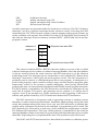
During execution of a push operation, first the content of the register is transferred
to the location in memory pointed at by SP, then the content of SP is decremented by
one. Let us examine now the contents of memory after the execution a PSHA instruction
address n-1
address n
unused
content
of A
SP points here after PSHA
SP points here before PSHA
As it can be clearly seen, the stack pointer always points to an empty or unused
location in memory.
During execution of a pull register operation, first the content of SP is incremented
by one, then contents of memory are transferred from the location in memory pointed
at by SP to register. Let us examine now the contents of memory after the execution of
PULA instruction
15
address n-1
address n
unused
content
of A
SP points here before PULA
SP points here after PULA
Register to register moves make use of the inherent addressing mode, since source
and destination address are already defined in the instruction.
TAP
TAX
TSX
Transfer A to CCR
Transfer A to X
Transfer SP+1 to H:X
TPA
TXA
TXS
Transfer CCR to A
Transfer X to A
Transfer H:X-1 to SP
TAP transfers the contents of the accumulator to the condition code register CCR.
Note that the bits 5 and 6 of the CCR are always set to one, and the TAP instruction
therefore can modify only bit 7 and bits 4 to 0. TPA however transfers all CCR bits to
the accumulator. TPA in conjunction with TAP is used to temporarily save condition
code register contents before execution of a program segment, which should not modify
the contents of the CCR, and restore contents after. Example code would look like
TPA
PSHA
////
PULA
TAP
where //// represents any number of lines of code.
TAX transfers the contents of accumulator to X, that is, duplicates A's contents to
the low byte of the index register. TXA just does the reverse of the TAX instruction.
The TAX instruction has been placed into the HC05 family of processors instruction
set to emulate “accumulator-offset indexed” addressing. Note that the HC05 family
has just an 8-bit index register, and zero offset, 8-bit offset, and 16-bit offset indexed
addressing can span a data array of 256 byte size maximum anywhere in memory. If,
for example, a program has to retrieve the nth data byte of an array starting at address
$E400, where n is contained in the accumulator, we could write he following piece of
code to solve the task:
TAX
LDA
$E400,X
The HC08 family of processors however have a 16-bit index register H:X. To use the
above code for a HC08 family processor, the high portion of the index register H has
to be cleared first using a CLRH instruction.
TSX and TXS are 16 bit transfers between stack pointer and index register and
need special attention. TSX transfers contents of the stack pointer plus one into the
index register, and not its own content. This instruction makes the index register point
16
to the last item pushed onto stack. It is good programming practice to use stack for
variables, temporaries and scratch area and not some absolute memory area of the
microcomputer. In such case all input data will be pushed onto stack and additional, if
necessary, scratch area reserved on stack. Then using TSX the index register will point
to the area of stack memory where all data is stored. At exit, all stack area has to be
restored. Example code would look like
PSHX
PSHH
PSHA
TSX
LDA
////
1,X
Here LDA 1,X would load the saved value of H into the accumulator. Note that in
this way any data on stack can be accessed in random order.
address n-3
address n-2
address n-1
address n
unused
content
of A
content
of H
content
of X
SP points here after PSHA
H:X points here after TSX
SP points here before PSHX
The programmer has to restore the stack by pulling off the stack the same number of
bytes pushed.
TXS transfers contents of index register minus one into the stack pointer, and is
complement instruction of TSX. TXS is a very infrequently used instruction and can be
used only to initialize the stack pointer from the index register value. This is very
useful since hardware reset initializes SP to $00FF. The 68HC908GP32 microcontroller
has 512 bytes of RAM in the address range $0040 to $023F. The following two lines of
code would initialize the SP to $023F.
LDHX
TXS
#$0240
Point to top of RAM of 68HC908GP32
H:X - 1 => SP
To move data between different memory locations usually a load source data to
accumulator, then store accumulator content to destination operation with one LDA
and STA instruction in sequence was performed. This was typical for most
microprocessors and microcontrollers. Since microcontrollers execute in majority move
type instructions to move data bytes between memory and on-chip peripherals located
in the first 256 bytes of address range, a new instruction MOV has been implemented
with the HC08 family of microcontrollers. This speeds up processing and shortens
code length. MOV moves a byte of data from a source address to a destination address
without the use of the accumulator. Data is examined as it is moved, and condition
code bits are updated. Source data is not changed. To specify source and destination
17
four addressing modes for the MOV instruction are defined as follows:
1.
2.
3.
4.
IMM/DIR moves an immediate byte to a direct memory location.
DIR/DIR moves a direct location byte to another direct location.
IX+/DIR moves a byte from a location addressed by H:X to a direct location.
H:X is incremented after the move.
DIR/IX+ moves a byte from a direct location to one addressed by H:X. H:X
is incremented after the move.
Let us give some simple examples to show the advantages of the MOV instruction.
First let us initialize PortA and PortB of the 68HC908GP32 located at addresses $00
and $01 in page 0 respectively. Using load and store instructions we would write
LDA
STA
LDA
STA
#$55
$00
#$AA
$01
Load accumulator with value
Save accumulator
Load accumulator with value
Save accumulator
2 ~/2 bytes
3 ~/2 bytes
2 ~/2 bytes
3 ~/2 bytes
This code would use up 8 bytes in memory and execute in 10 cycles. Using the MOV
instruction
MOV
MOV
#$55,$00
#$AA,$01
Move $55 to location $00
Move $AA to location $01
4 ~/3 bytes
4 ~/3 bytes
the same program would require only 6 bytes and execute in 8 cycles. If the above
load store sequence should not have modified the accumulator, a PSHA has to used
before the LDA #$55 instruction and a PULA has to follow the STA $01 instruction,
lengthening the code and slowing it down further.
Let us now give a more complex example where an array of bytes starting at
location BEGIN and ending at location END, are to be sent byte by byte to Port A of
the 68HC908GP32 microcontroller. Using the MOV instruction, the code would look
like
LOOP
LDHX
MOV
CPHX
BLS
#BEGIN
X+,$00
#END
LOOP
Point to string in memory
move data from memory to Port A
has pointer reached END ?
if not, send next one
3 ~/3 bytes
4 ~/2 bytes
3 ~/3 bytes
3 ~/2 bytes
The instruction CPHX (ComPare H:X) compares H:X against the upper limit END and
updates the flags in the CCR. The instruction BLS (Branch if Lower or Same) tests
whether the CCR bits indicate a lower or same case for the compare operation or not.
The same task could be done using again load and store instructions and a separate
index register incrementation using AIX #1 as follows
LOOP
LDHX
LDA
STA
#BEGIN
,X
$00
Point to string in memory
Get data from memory
Store data to Port A
18
3 ~/3 bytes
2 ~/1 byte
3 ~/2 bytes
AIX
CPHX
BLS
#1
#END
LOOP
increment H:X by 1
has pointer reached END ?
if not, send next one
2 ~/2 bytes
3 ~/3 bytes
3 ~/2 bytes
using up more memory for program code and executing slower.
2-4-2
Arithmetic Instructions
The computer is often used to compute numerical data, as the name implies, or to
control a process or machinery. These operations need arithmetic instructions, which
we will now study. However, you must recall that computers are designed and programs
are written to enhance static or dynamic efficiency. Rather than having four basic
arithmetic instructions - add, subtract, multiply, and divide - computers have
instructions that occur most often in programs. Rather than the sophisticated divide,
we will see the often used increment and decrement instruction in a computer. It is
also a fact that the ability to execute multiply and divide instructions needs a high
amount of additional hardware in the arithmetic-logic unit, but today VLSI technology
easily allows us to do so. In control and data acquisition applications multiplication
and division are frequently used, and due to this fact, the Motorola HC08 family of
microcontrollers got a 8 x 8 multiply and a 16 / 8 divide instruction. Arithmetic
instructions make use of the immediate, direct, indexed, extended, and inherent
addressing modes. Let us first look at addition and subtraction.
ADD
ADC
ADD to accumulator
ADd with Carry to accumulator
SUB
SBC
SUBtract from accumulator
SuBtract with Carry from accumulator
As it can be easily seen, there are two types of addition and subtractions, namely
with and without carry. Addition without carry adds contents of memory to the
relevant accumulator. The addition can generate a carry, since input and output of the
operation have to fit to same size. All conditional results of the addition are reflected
in the bits of the condition code register. Addition with carry adds contents of memory
and the carry bit to the accumulator and may generate also a carry. Due to this fact,
addition with carry is used if multi-byte sized numbers are to be added. Let us have
three examples to add 24-bit (3 byte) numbers. The full assembly listing below shows
memory location, machine code, label area, instruction mnemonic, operand and optional
comment fields.
0100
0103
0106
0109
010C
010F
0112
C6
CB
C7
C6
C9
C7
C6
0182
0185
0188
0181
0184
0187
0180
ADD24
LDA
ADD
STA
LDA
ADC
STA
LDA
$0182
$0185
$0188
$0181
$0184
$0187
$0180
19
Save sum LSB
Save sum NSB
0115 C9 0183
0118 C7 0186
ADC
STA
$0183
$0186
ADD24
LDHX
LDA
ADD
STA
LDA
ADC
STA
LDA
ADC
STA
#$0180
2,X
5,X
8,X
1,X
4,X
7,X
,X
3,X
6,X
Point to MSB of source
Get LSB
add
Save sum LSB
LDHX
CLC
LDA
ADC
STA
DBNZX
#3
set loop counter
clear carry bit
get number
add with carry
store sum
decr. X, branch if not 0
0100
0103
0105
0107
0109
010B
010D
010F
0110
0112
45
E6
EB
E7
E6
E9
E7
F6
E9
E7
0180
02
05
08
01
04
07
0100
0103
0104
0107
010A
010D
45
98
D6
D9
D7
5B
0003
ADD24
0182
0185
0188
F5
ALOOP
03
06
$0182,X
$0185,X
$0188,X
ALOOP
Save sum MSB
In the first two examples, the least significant byte of the numbers are added without
carry, whereas the more significant bytes are added using carry. Since load and store
operations do not modify the carry bit, carry between additions is not lost. Note that
the program segment using extended addressing needs 27 bytes and executes in 36
clock cycles, compared to 20 bytes and 29 clock cycles for the indexed mode including
initialization of the index register. The third example making use of 16-bit offset
indexed addressing and using the X register also as a loop counter. The DBNZX
instruction is a looping primitive decrementing X by one and testing the Z flag of the
CCR. If the Z flag is not set, that is, X has not reached zero, a branch to the given label
is made. This short code needs only 15 bytes for the task but due to 16-bit offset
indexed addressing timing and the DBNZX instruction overhead 48 clock cycles are
needed. Note that a CLC instruction is used before the loop performing additions
with carry. This code is only efficient for large loop counts.
Another interesting example would be data manipulation on stack as shown below:
PSHX
PSHH
PSHA
TSX
ADD
STA
CLRA
ADC
STA
PULA
PULH
2,X
2,X
1,X
1,X
20
PULX
Examining stack after the TSX instruction executed, we would see
address
unused
SP points here after
address
pushed A
H:X points here after
address
pushed H
address
pushed X
SP points here before PSHX
This small program segment does an effective address calculation adding the
unsigned 8-bit value in the accumulator to the index register (H:X). Since there is no
instruction available which can add the contents of A to H:X, the contents of H:X has
to be saved first in memory to allow a memory to register addition operation. After
TSX the index register points to the memory location, where the accumulator has been
saved by PSHA. Now, using first the ADD 2,X (ADD memory content to accumulator)
instruction in indexed addressing mode and with one offset, we obtain A = A + X. We
save this sum using STA 2,X again onto stack and overwrite the previous value of X.
The possible carry C, generated during the addition of A and X is still in the CCR.
After zeroing A by executing CLRA and then by ADC 1,X adding A to H (H contained
in memory at 1,X) together with the possible carry of the previous addition, the
content of A will be either equal to the original H or H+1. We save this sum using STA
1,X again onto stack and overwrite the previous value of H. Now the stack looks like
address n-3
unused
address n-2
A
address n-1
C+H
address n
A+X
SP points here after PSHA
H:X points here after TSX
SP points here before PSHX
Executing finally in sequence PULA, PULH and PULX instructions, the memory contents
in stack are transferred to the A and H:X registers, and the stack pointer is also
updated to point to the memory location at program start.
Having explained addition in detail, there is no need to give examples for
subtraction, since the code writing principles are identical. A slight variant of the
subtract operation, the comparison however needs special attention.
Compare instructions compare contents of registers against memory contents.
These instructions perform also subtractions, but do not write the resulting difference
into the associated register. They just update the CCR flags as if a subtraction was
done.
21
CMP
CPHX
CPX
CoMPare accumulator against content of memory
CoMPare index register H:X against content of memory
ComPare X register against content of memory
The CMP and CPX instructions are 8-bit comparisons whereas the CPHX is a 16-bit
comparison. Let us give a simple example which checks Port A contents against a
limit. If Port A is less than or equal the limit value, set Port B equal to 1, else equal to 2.
High
Save
LDA
CMP
BHI
LDA
BRA
LDA
STA
#$7F
$00
High
#1
Save
#2
$01
Set comparison value
Read Port A
go to High if value is higher
else set A = 1
go to Save
Set A = 2
Save A in Port B
This program segment makes the assumption that Port A and Port B have been initialized
to act as input and output respectively. To clear memory locations starting at $0040
and ending at $01FF the following simple code can be used:
CLRM
CLOOP
LDHX
MOV
CPHX
BLS
#$0040
#0,X+
#$01FF
CLOOP
Let H:X point to first location
move $00 to memory, increment H:X
compare H:X against upper limit
branch to CLOOP if lower or same
A special case of the compare instructions are the TST instructions
TSTA
TSTX
TST
TeST Accumulator
TeST X register
TeST content of memory
which do an immediate compare against zero of the accumulator, index low byte or
memory. These instructions modify the zero and minus flags and reset the overflow
flag in the CCR.
As noted earlier, some arithmetic instructions are included in the instruction set
to enhance static and dynamic efficiency. We often add 1 to or subtract 1 from an
accumulator or a byte in memory, say to count the number of times that something is
done. Rather than use an ADD instruction with an immediate value of #1, a shorter
instruction INCA is used for these many instances. The increment and decrement
instructions
INCA
INCX
INC
INCrement A
INCrement X
INCrement content of memory
DECA
DECX
DECrement A
DECrement X
22
DEC
DECrement content of memory
add or subtract 1 from A, X or a memory location. Examining the flags, it seems a little
puzzling that the carry bit is unaffected by an INC or DEC instruction. Since INC or
DEC are usually used to update a loop counter, these instructions are used for counting,
and not directly for arithmetic. Since any memory cell can be used for this purpose, a
large number of counters can be easily constructed without using the A and X registers.
Two slightly different addition like instructions are the
AIX
AIS
Add immediate to H:X register
Add immediate to SP register
instructions to add a signed 8-bit value immediately to the contents of the H:X or SP
registers respectively. With this instruction it is possible to decrement or increment
the H:X or SP register in the range -128 to +127. Note that these instructions do not
change any flags, since they are just pointer modifiers. The AIS instruction can be
used to create and remove a stack frame buffer that is used to store temporary variables.
The following example shows how to load into A content of location pointed at by
H:X plus A. H:X is preserved.
PSHX
PSHH
PSHX
PSHH
ADD
TAX
PULA
ADC
PSHA
PULH
AIS #1
LDA
PULH
PULX
Save original H:X on stack
Push X then H onto stack
2,SP
#0
,X
Add stacked X to A
Move result into X
Pull stacked H into A
Take care of any carry
Push modified H onto stack
Pull back into H
Clean up stack
th
Get A element of array
Restore original H:X
This operation emulates a LDA A,X instruction, which is not available in the HC08
family instruction set. This addressing mode, the so called accumulator-offset indexed
addressing mode, simplifies data operations on arrays dramatically.
Most of the control, data acquisition and signal processing algorithms use in
addition to addition and subtraction, multiplication and division. The implementation
of hardware multiplier and divider required a very large number gates in the ALU
increasing the chip area and thereby the cost. The first microcontroller to incorporate a
hardware multiplier was the Motorola MC6801. Later, as VLSI technology advanced,
more complex microcontrollers like the MC68HC11 were designed, which also
incorporated a hardware divider. The HC08 family of microcontrollers, built using the
latest VLSI technologies, can easily incorporate the hardware multiplier and divider.
23
The 8 by 8 multiply instruction MUL, multiplies A and X, and stores the 16-bit product
in X:A, i.e. overwriting original multiplier and multiplicand. The carry bit is cleared
after this operation.
DIV divides a 16-bit unsigned dividend contained in the concatenated registers H
and A by an 8-bit divisor contained in X. The quotient is placed in A, and the remainder
is placed in H. The divisor is left unchanged. An overflow (quotient > $FF) or divide-by-0
sets the C bit, and the quotient and remainder are indeterminate.
Arithmetic in microprocessors is mostly done in binary or hexadecimal notation
because of the higher byte efficiency. However, for human interfacing decimal notation
is more practical. The DAA instruction, for decimal adjust accumulator, is used when
binary-coded decimal numbers are being added. Briefly, two decimal digits per byte
are represented with binary-coded decimal, the most significant four bits for the most
significant digit and the least significant four bit for the least significant digit. Each
decimal digit is represented by its usual 4-bit expansion so that the 4-bit sequences
representing 10 through 15 are not used. Only addition instructions affect the half-carry
bit to enable binary-to-BCD conversion by the DAA instruction. To see how the decimal
adjust works, suppose that the hexadecimal contents of A is $46 and the hexadecimal
contents of location $0140 is $27. After
ADD $0140
is executed, the contents of A will be $6D and the carry bit will be zero. However, if
we are treating this numbers as binary-coded decimal numbers, what we want is $73
in A. The sequence
ADD $0140
DAA
does just that. The DAA instruction may be used only after ADD or ADC instructions.
Negation, subtracting a number from 0, is done often enough that it merits a
special instruction. The instructions
NEGA
NEGX
NEG
NEGate A
NEGate X
NEGate content of memory
subtract the 8-bit number in A, X or a memory location from zero, placing the result in
the same place as the operand. The bits C, N, Z, and V are modified for this operation.
Clearing, or writing a 0 to a destination, is a very important instruction to preset a
memory location or register. The bits N and V are cleared and Z is set. C is unchanged.
CLRA
CLRX
CLR
CLeaR A
CLeaR X
CLeaR content of memory
24
2-4-3
Logic Instructions
Logic instructions are used to set, clear or modify individual or multiple bits or
bit patterns in accumulators, registers and memory. They are used by compilers,
program that translate high-level languages to machine code, to manipulate bits to
generate machine code. They are used by controllers of machinery because bits are
used to turn things on and off. They are used by operating systems to control
input/output (I/O) devices and to control allocation of time and memory on a computer.
Combinatorial logic instructions of the HC08 are
AND
ORA
EOR
AND A
OR A
Exclusive OR A
and the one's complement of an accumulator or memory byte
COMA
COMX
COM
COMplement A
COMplement X
COMplement content of memory
A variant of the AND instruction is the BIT instruction, the same way the CMP
instruction is compared with the SUB instruction. The BIT
BIT
BIT test A
instructions logically and the contents of memory with the respective accumulator,
update the N and Z flag, reset the V flag bit, but do not change the contents of the
accumulator in use.
In microcontroller applications we frequently have to clear or set a specific bit of
available ports. This can be accomplished by using the AND and ORA instructions
respectively. Let us for example write a small segment of code to clear bit 3 of Port A
and to set bit 0 of Port B as follows
LDA
AND
STA
LDA
ORA
STA
$00
#$FB
$00
$01
#$01
$01
Read Port A data
AND A with $FB to clear bit 3
Store data in Port A
Read Port B data
OR A with $01 to set bit 0
Store data in Port B
3~/2 bytes
2~/2 bytes
3~/2 bytes
3~/2 bytes
2~/2 bytes
3~/2 bytes
As can be seen each operation takes three lines of code with a total execution time of
16 clock cycles and a size of 12 bytes of memory. To shorten and speedup code two
new instructions
BCLR n
Clear Bit n in Memory
25
BSET n
Set Bit n in Memory
have been added to the instruction set. Rewriting the above code we would obtain
BCLR
BSET
3,$00
0,$01
Clear bit 3 of location 0
Set bit 0 of location 1
4~/2 bytes
4~/2 bytes
speeding up the execution by a factor two and reducing memory requirement by a
factor 3. Note that this two new instructions do not modify any CCR bits and the
memory has to be in direct page (first 256 locations). All microcontrollers of the HC08
family have I/O located in direct page.
Shift and rotate instructions are a special group of logic instructions, rearranging
bits of data in an accumulator, X register or memory byte. For example, the arithmetic
shift-left instruction
ASLA
ASLX
ASL
Arithmetic Shift Left A
Arithmetic Shift Left X
Arithmetic Shift Left content of memory
shifts all the bits left by one, putting the most significant bit into the carry bit of the
CCR, and putting a zero in on the right.
C
0
b7
b0
The mnemonics
LSLA
LSLX
LSL
Logic Shift Left A
Logic Shift Left X
Logic Shift Left content of memory
are synonyms of the ASLx instructions, because an arithmetic shift-left is equivalent to
a logic shift. Shifting all bits up (to the left) is equal to a multiplication by two.
In the shift-right operation of an accumulator, X register or memory byte, there
exists a major difference between an arithmetic and logic operation. The arithmetic
shift-right instructions
ASRA
ASRX
ASR
Arithmetic shift right A
Arithmetic shift right X
Arithmetic shift right content of memory
shift all bits right by one, holds the most significant bit in its position, and puts the
least significant bit into the carry bit of the CCR.
26
C
b7
b0
Holding the most significant bit in place, the sign is preserved, and therefore this
instruction acts as a signed divide-by-two operation. Assuming the contents of the
accumulator to be $80 (-128 decimal) before the ASRA instruction, it can be seen that it
will be $C0 (-64 decimal) after.
The logic shift-right is just the complement of the shift-left operation, shifting all
bits right by one, putting the least significant bit into carry, and putting a zero in on
the left. This if analyzed, is equivalent to an unsigned divide-by-two.
LSRA
LSRX
LSR
Logic Shift Right A
Logic Shift Right X
Logic Shift Right content of memory
C
0
b7
b0
Rotate instructions, like shift instructions, shift the bits in the accumulator, X
register or memory byte. However, while the carry bit is shifted in on one side, the bit
on the other side is shifted out into carry. Due to this circular operation, these instructions
are called rotate instructions.
ROLA
ROLX
ROL
ROtate Left A
ROtate Left X
ROtate Left content of memory
C
b7
RORA
RORB
ROR
b0
ROtate Right A
ROtate Right X
ROtate Right content of memory
C
b7
b0
Rotate instructions are used with multiple-byte arithmetic operations such as
division with and multiplication by two. For example, the sequence
ASL
ROL
ROL
$0102
$0101
$0100
27
multiplies the 24-bit number in memory locations $0100 - $0102 by two.
Another important code simplifying instruction is NSA, nibble swap accumulator.
This instruction exchanges the two halves of the accumulator. The NSA instruction is
used for more efficient storage and use of binary-coded decimal operands. The following
code will compress two bytes, each containing one BCD nibble, into one byte in A.
Each byte contains the BCD nibble in bits 0-3. Bits 4-7 are clear.
LDA
NSA
ADD
BCD1
BCD2
Read first BCD byte
Swap LS and MS nibbles
Add second BCD byte
If NSA had not been incorporated in the instruction set we had to realize the
above code as follows:
LDA
LSLA
LSLA
LSLA
LSLA
ADD
BCD1
BCD2
The remaining logic instructions
CLC
CLI
CLV
CLear Carry bit
CLear Interrupt bit
CLear oVerflow bit
SEC
SEI
SEV
SEt Carry bit
SEt Interrupt bit
SEt oVerflow bit
are used to clear or set individual bits in the condition code register.
2-4-4
Control instructions
The next class of instructions, the control instructions or program flow control
instructions, are those that affect the program counter. After the move class, this class
composes the most often used instructions. Control instructions are divided into
branching instructions and what might be called subroutine and interrupt instructions.
Let us discuss branching instructions first. Branching instructions all use relative
addressing. A source program specifies the destination of a branch instruction by its
absolute address, either as a numerical value or as a symbol or expression which can
be numerically evaluated by the assembler. The assembler calculates the 8-bit relative
offset as the difference from this absolute address and the current value of the location
counter. During program execution, if the tested condition is true, the two’s complement
offset is sign-extended to a 16-bit value which is added to the current program counter.
This causes program execution to continue at the address specified as the branch
destination. If the tested condition is not true, the program simply continues to the
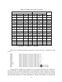
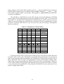
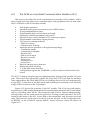
next instruction after the branch. Table 2-1 gives a summary of all branch instructions.
28
There are two unconditional and 18 conditional branch instructions. For example,
the instruction
BRA
Label
for “branch always” will cause the program counter to be loaded with the address
“Label”. Corresponding to the BRA instruction the instruction
BRN
Label
for “branch never” will never branch to location “Label”. This instruction seems to be
useless at the first glance, but it is useful because any branching instruction can be
changed to a BRA or BRN instruction just by changing an opcode byte. This allows a
programmer to choose manually whether a particular branch is taken while he or she
is debugging a program.
Conditional branch instructions test the condition code bits. As noted earlier these
bits have to be carefully watched, for they make a program look so correct that you
want to believe that the hardware is at fault. The hardware is rarely at fault. The
condition code bits are often the source of the fault because the programmer mistakes
where they are set, and which ones to test in a conditional branch. See the right
column of the operation code bytes table in Appendix 1. Note that move instructions
generally change the N and Z flag bits, but not the C bit, or change no bits at all;
arithmetic instructions generally change all five bits H, N, Z, V, and C; logic instructions
generally change the N, Z and C flag bits. There is sound rationale for which bits are
affected, and the way they are changed.
29
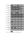
Table 2-1. Branch Instruction Summary
Branch
Complementary Branch
Type
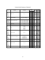
Mnemonic Opcode
Test
Mnemonic Opcode
Test
Boolean
r>m
(Z)∩(N⊕V)=0
BGT
92
r≤m
BLE
93
Signed
r≥m
(N⊕V)=0
BGE
90
r<m
BLT
91
Signed
r=m
(Z)=1
BEQ
27
r≠m
BNE
26
Signed
r≤m
(Z)∩(N⊕V)=1
BLE
93
r>m
BGT
92
Signed
r<m
(N⊕V)=1
BLT
91
r≥m
BGE
90
Signed
r>m
(C)∩(Z)=0
BHI
22
r≤m
BLS
23
Unsigned
r≥m
(C)=0
BHS/BCC
24
r<m
BLO/BCS
25
Unsigned
r=m
(Z)=1
BEQ
27
r≠m
BNE
26
Unsigned
r≤m
(C)∩(Z)=1
BLS
23
r>m
BHI
22
Unsigned
r<m
(C)=1
BLO/BCS
25
r≥m
BHS/BCC
24
Unsigned
Carry
(C)=1
BCS
25
No carry
BCC
24
Simple
result=0
(Z)=1
BEQ
27
result≠0
BNE
26
Simple
Negative
(N)=1
BMI
2B
Plus
BPL
2A
Simple
I mask
(I)=1
BMS
2D
I mask=0
BMC
2C
Simple
H-bit
(H)=1
BHCS
29
H=0
BHCC
28
Simple
IRQ high
–
BIH
2F
IRQ low
BIL
2E
Simple
Always
–
BRA
20
Never
BRN
21
Uncond.
explanations : (…) contents of ; ∩ logic AND
There are 10 simple branching instructions, which test only a single bit of the
CCR.
BNE
BEQ
BPL
BMI
BCC
BCS
BHCC
BHCS
BIL
BIH
Label
Label
Label
Label
Label
Label
Label
Label
Label
Label
Branches to location Label if Z = 0
Branches to location Label if Z = 1
Branches to location Label if N = 0
Branches to location Label if N = 1
Branches to location Label if C = 0
Branches to location Label if C = 1
Branches to location Label if H= 0
Branches to location Label if H = 1
Branches to location Label if the IRQ pin is low
Branches to location Label if the IRQ pin is high
Frequently, two numbers are compared, as in a compare instruction or a subtraction.
One would like to make a branch based on whether the result is positive, negative,
less than, and so forth. The table below, where R stands for the contents of a register
and M stands for the contents of a memory location (or locations), shows the test and
the branching statement to make depending on whether the numbers are interpreted
30
as signed or unsigned.
Test
Signed
Unsigned
R<M
R ≤ MBLE
R ≥ MBGE
R>M
BLT
BLS
BHS (or BCC)
BGT
BLO (or BCS)
_________________________________________________________________
BHI
The branch mnemonics for the two's complement, or signed, number are
BLT
BLE
BGE
BGT
Branch if Less Than
Branch if Less than or Equal to
Branch if Greater than or Equal to
Branch if Greater Than
Branch if N ⊕ V = 1
Branch if Z + (N ⊕ V) = 1
Branch if N ⊕ V = 0
Branch if Z + (N ⊕ V) = 0
The mnemonics for unsigned numbers are
BLO
BLS
BHI
BHS
Branch if LOwer
Branch if Lower or Same
Branch if HIgher
Branch if Higher or Same
Branch if C = 1
Branch if C + Z = 1
Branch if C + Z = 0
Branch if C = 0
Notice that BLO is the same instruction as BCS, and BHS is the same instruction as
BCC. One should consult the instruction set summary in Appendix 1 for a while to
make sure that the correct branch is being chosen. Each of the preceding branch
statements is represented in memory by an opcode byte followed by the 1-byte two's
complement relative offset. Note that due to the one-byte two's complement offset, the
maximum displacements are limited to +127 and -128. Larger displacements can be
spanned using additional BRA instructions, although this rather seldom happens.
Notice also that a branch for 2’s complement overflow is missing. It can be
implemented by the following code segment
V_SET
TPA
TSTA
BMI
////
////
V_SET
code if V is not set
code for case when V is set
since the V flag is the most significant bit of the CCR.
In addition to the branch instructions there are some additional instructions which
combine two operations in one. These are
BRCLR n
BRSET n
CBEQ
BRanch if bit n in memory CLeaR
BRanch if bit n in memory SET
Compare and Branch if EQual
31
CBEQA
CBEQX
DBNZ
DBNZA
DBNZX
Compare A with immediate operand and Branch if EQual
Compare X with immediate operand and Branch if EQual
Decrement content of memory and Branch if Not Zero
Decrement A and Branch if Not Zero
Decrement X and Branch if Not Zero
The BRCLR n instruction tests bit n of a memory location in direct page and if
clear branches to the given label. If the tested bit is not clear, the instruction following
the BRCLR n instruction is executed. The BRSET n instruction tests bit n of a memory
location in direct page and if set branches to the given label. If the tested bit is not set,
the instruction following the BRSET n instruction is executed.
CBEQ compares the operand with the accumulator (or index register for CBEQX
instruction) against the contents of a memory location and causes a branch if the
register (A or X) is equal to the memory contents. The CBEQ instruction combines
CMP and BEQ for faster table lookup routines and condition codes are not changed.
The IX+ variation of the CBEQ instruction compares the operand addressed by
H:X to A and causes a branch if the operands are equal. H:X is then incremented
regardless of whether a branch is taken. The IX1+ variation of CBEQ operates the
same way except that an 8-bit offset is added to H:X to form the effective address of
the operand.
Let us now have a simple piece of code to skip spaces ($20) in a string of ASCII
characters. The string must contain at least one non-space character and it is assumed
that on entry the H:X register points to start of string and at exit H:X points to first
non-space character in the string.
SKIP
*
LDA
CBEQ
#$20
X+,SKIP
AIX
#-1
Load space character
Increment through string until
non-space character found.
Adjust pointer to point to 1st non-space char.
Note that X post increment will occur irrespective of whether branch is taken or not.
In this example, H:X will point to the non-space character plus 1 immediately following
the CBEQ instruction.
CBEQA and CBEQX compare accumulator or index low byte against an immediate
operand in memory and branch if the operand is equal to the respective register
content.
The looping primitives DBNZ, DBNZA and DBNZX subtract 1 from the contents
of memory, A, or X; then branch using the relative offset if the result of the subtraction
is not $00. DBNZX only affects the low order eight bits of the H:X index register pair;
the high-order byte (H) is not affected. An example for DBNZX was given earlier in
section 2-4-2 along with the ADD and ADC instructions.
The BRA instruction making use of indexed and extended addressing instead of
32
relative addressing is called the JMP “Jump” instruction. The effective address is
retrieved from memory by the locations using the index register contents plus the
unsigned offset in the indexed mode or by directly specifying the explicit 16-bit address
in the extended mode.
The indexed mode of addressing for the jump instruction is of particular importance,
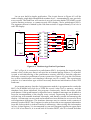
since it eases the use of jump tables. For example, let us write a small program
segment, where the program should jump to the nth table address, called a vector.
Assume that at sequence entry, accumulator contents is n = 2, and H:X points to the
beginning of the vector address table (Vector 0) in memory.
Table start
Vect.0H
Initial H:X register
Vect.0L
Vect.1H
Vect.1L
Vect.2H
H:X points here after addition
Vect.2L
LSLA
PSHX
PSHH
ADD
TAX
PULA
ADC
PSHA
PULH
PULA
LDA
LDX
PSHA
PULH
JMP
Multiply A by two
Push X then H onto stack
2,SP
#0
,X
1,X
,X
Add stacked X to A
Move result into X
Pull stacked H into A
Take care of any carry
Push modified H onto stack
Pull back into H
Clean up stack
Get Vector high byte into A
Get Vector low byte into X
Copy A into H
Jump to program at vector address
The accumulator has to be multiplied by two before addition to the index register H:X,
since each entry in the vector table is of two byte length. Since the indexed addressing
mode for LDHX is missing we cannot load H:X with the content of memory H:X is
pointing at. To do so, we load A with the high byte of the vector address using
indexed addressing with zero offset, and load X with the low byte of the vector
address using again indexed addressing, but with an offset of one. After copying A to
H via push and pull operations, H:X contains the vector address. Now the indexed
jump can be performed.
Finally there is one more unconditional branch instruction, the “No Operation”
33
NOP instruction. This instruction does nothing, but increments the program counter.
It can be used to tune delay loops, as this example can show:
DLOOP
CLRA
NOP
NOP
DECA
BNE
Preset loop count to 256
DLOOP
Without the two NOP instructions the loop would execute in 4 clock cycles, and the
total delay would be 256 x 4 = 1024 clock cycles. However, with the NOP instructions
inserted the loop time increased to 6, and the total delay to 256 x 6 = 1536 clock cycles.
You may have already written a program where one segment of it is repeated in
several places. Have you wished that you knew how to avoid writing it more than
once? Two solutions exist, the first is called a subroutine call, the second a macro
definition. We will deal now with the first solution, the subroutine call. A subroutine
is a program segment which ends with an instruction such that the subroutine program
will return to the main calling program. This return instruction has to retrieve
information where the main program has to be continued, and has to load the program
counter with this value. For this purpose subroutine call instructions save the address
of the instruction immediately following the subroutine call instruction onto hardware
stack, low byte first, and load the program counter with the address of the called
subroutine; the RTS “return from subroutine” instruction causes the top two bytes of
the hardware stack to be pulled back into the program counter, high byte first. In
order to guarantee proper operation of the subroutine call and return instruction pair,
the programmer has to assure that the saved program counter has to be on top of
stack at the time the RTS instruction is executed.
34
Machine code for
subroutine call
Next instruction
of main program
•
•
•
Machine code for
subroutine call
Next instruction
of main program
•
•
•
Subroutine
program start
•
•
•
Machine code for
subroutine return
$81
Figure 2-2. Subroutine call and return
The Motorola HC08 family has two subroutine call instructions:
BSR
JSR
Branch to SubRoutine
Jump to SubRoutine
The BSR instruction makes use of relative addressing, whereas the JSR instruction
makes use of direct, indexed, and extended addressing.
Addition and subtraction of 8-bit numbers is simple matter for the HC08
programmer. 8 by 8 multiplication is also done using the MUL instruction and 16 by 8
division is realized using the DIV instruction. However, multiplication of say two
16-bit numbers yielding a 32-bit result, or other more complex but frequently used
routines or algorithms can be written down as subroutines to be called from anywhere
in your main program.
The last group of control instructions are made up of interrupt instructions. These
instructions, like subroutine instructions temporarily give up control of the main
program, execute the particular code segment, and finally return back to resume main
program execution. Interrupt instructions save all registers except the H register and
the stack pointer onto hardware stack in contrast to subroutine call instructions. There
are three related interrupt instructions:
35
SWI
WAIT
STOP
RTI
SoftWare Interrupt
Enable interrupts; stop CPU
Enable interrupts; Stop Clock Oscillator
ReTurn from Interrupt
Actually interrupts are generated either by hardware or software. The SWI “Software
Interrupt” serves to generate interrupts under software control. Executing the SWI
instruction the CPU will first stack register contents starting with program counter up
to the condition code register, then set the I bit in the CCR, and finally read contents of
the software interrupt vector at memory locations $FFFC : $FFFD and load it into the
program counter.
SP points here after SWI
address n-5
address n-4
CCR
A
X
PC H
address n
PC L
SP points here before SWI
The value in locations $FFFC : $FFFD is the start address or vector of the so called
software interrupt service routine or software interrupt handler. Since the start address
is always retrieved from the same locations, the SWI instruction is of the inherent
addressing mode. The interrupt service routine has to end with the RTI “Return from
Interrupt” instruction, which pulls off stack registers saved. The SWI instruction is
primarily used to insert a so called breakpoint into a user program. A breakpoint is a
point in the program, where normal execution stops, and the monitor program gains
temporarily control of the system to enable debugging. After having checked the
program, the user can return from the breakpoint and resume normal program execution.
For HC05 family compatibility, the SWI instruction and hardware interrupts do not
stack the H register. If however, the interrupt service routine is to change the H
register, it has to be stacked by a PSHH instruction at the beginning of the service
routine, and pulled off stack by a PULH instruction before the RTI instruction.
The SWI instruction is frequently used in operating systems to emulate system
functions or other nonexisting instructions. Emulation means getting exactly the same
result, but perhaps taking more time. Since only one SWI instruction is defined, but
usually many operations are desired to be emulated, a programming trick is used: The
SWI instruction is followed by a data byte, which enables the programmer to define
256 different SWI operations. This byte, called postbyte, is interpreted in the software
interrupt handler routine, and control is given to the particular interrupt service routine
thereafter. Explaining how to implement this trick is beyond the scope of this book.
The WAIT and STOP instructions have been added to enable two different power
36
saving states. Executing the WAIT instruction, the MCU first clears the I bit in the
CCR, thereby enabling maskable hardware interrupts, then stops the clock of the
CPU, but not the clocks of the peripherals. Stopping the CPU reduces the power
consumption by an important amount. Any peripheral having the capability to generate
interrupts, can upon interrupt reactivate CPU clocks. After CPU clocks are activated,
the CPU will stack its registers, and then fetch the appropriate interrupt vector to start
the interrupt service routine. Executing the STOP instruction however, the MCU will
first clear the I bit in the CCR, then it will stop to clock oscillator. This will stop
everything in the MCU, reducing power consumption to almost zero. A hardware
interrupt applied via the IRQ pin or resetting the MCU will reactivate the clock generator.
Reactivation of the clock is a lengthy process, since the clock generator has to stabilize.
Details about power saving modes and instructions will be covered in later chapters.
Increasing priority
Table 2-2. MC68HC908GP32 MCU Interrupt Vector Locations
MSB
LSB
Interrupt
RESET
FFFE FFFF
FFFC FFFD Software Interrupt (SWI)
IRQ Pin
FFFA FFFB
CGM (PLL)
FFF8 FFF9
TIM1 channel 0
FFF6 FFF7
TIM1 channel 1
FFF4 FFF5
TIM1 overflow
FFF2 FFF3
TIM2 channel 0
FFF0 FFF1
TIM2 channel 1
FFEE FFEF
TIM2 overflow
FFEC FFED
FFEA FFEB
SPI receiver
FFE8 FFE9
SPI transmitter
FFE6 FFE7
SCI errors
FFE4 FFE5
SCI receiver
FFE2 FFE3
SCI transmitter
FFE0 FFE1
KBD pin
FFDE FFDF
A/D conv. comp.
FFDC FFDD
Timebase
Table 2-2 gives a complete listing of all interrupt vectors of the MC68HC908GP32
microcontroller. RESET has the highest priority among all interrupts followed by SWI
and IRQ pin. RESET has the highest priority since it is recognized immediately
immaterial of the state of the MCU. Since SWI can be executed independent of the
state of the I-bit, it has the next highest priority. Among all hardware interrupts,
which are maskable, the IRQ pin has the highest priority. In the event that two or
more interrupts happen simultaneously, the interrupt having the higher priority will
37
be serviced first.
2-4-5
Input/Output Instructions
The last class of instructions, the input/output or I/O class, does not exist for
Motorola microprocessors and microcontrollers. All Motorola microcontrollers use
memory mapped I/O instead of independent I/O. Memory mapped I/O is superior
to independent I/O since all instructions which fetch one of their operands from
memory and/or store a result into memory can be used with I/O devices, i.e. all
move, arithmetic, and logic instructions can be used as I/O instructions.
2-5 Assembler Directives and Pseudo Operations
We have shown all instructions of the HC08 family. In order to write a program
that can be assembled, the assembler needs more information. For this purpose some
so called assembler directives and pseudo operations have been defined [2]. The most
frequent used are listed below:
DS #n
Define storage
END
EQU
FCB
End of source program
Equate
Form Constant Byte
FCC
FDB
MACR
MEND
ORG
RMB
Reserve n number of bytes in memory as specified
by operand,
Define label equal to operand,
Form a byte in memory with contents
of operand,
Form Constant Character Form ASCII character string in memory defined
in operand field,
Form Double Byte
Form double byte in memory with contents of
operand,
Macro Definition
Define a macro expression,
Macro Definition End
End macro expression,
Origin
Force program counter to contents of operand,
Reserve Memory Byte
Reserve number of bytes in memory as specified
by operand.
Please note that some non-standard macroassemblers need a semicolon instead of a
space character before the comment field. A more complete set of assembler directives
and pseudo operations can be found in 68HC08 In-Circuit Simulator Operator’s Manual
[2]. Using assembler directives, let us rewrite an example given before
PORTA
PORTB
*
EQU
EQU
$00
$01
Define value (address) of PORTA
Define value (address) of PORTB
ORG
LDA
AND
STA
$0100
PORTA
#$FB
PORTA
Force program to start at $0100
Read Port A data
AND A with $FB to clear bit 3
Store data in Port A
38
LDA
ORA
STA
END
PORTB
#$01
PORTB
Read Port B data
OR A with $01 to set bit 0
Store data in Port B
Having defined PortA and PortB earlier in the program by the EQU statements, the
code written is much easier to understand.
The following interrupt service routine will be run upon reception of a byte in the
serial communication interface SCI. The SCI receiver interrupt vector located at
$FFE4:$FFE5 points to the beginning of the SCI service routine SCISER. The FDB
assembler directive will force the assembler to evaulate the address of SCISER and put
its value into locations $FFE4:$FFE5. The two RAM locations $40 and $41 are reserved
by the assembler to be used as INBUF.
SCS1
SCS2
SCDR
*
INBUF
*
SCISER
EQU
EQU
EQU
$16
$17
$18
SCI status register 1
SCI status register 2
SCI data register
ORG
RMB
$40
2
Point to beginning of RAM
Storage area for input buffer pointer
ORG
LDA
LDHX
MOV
STHX
RTI
$E000
SCSI1
INBUF
SCDR,X+
INBUF
Point to SCI interrupt service routine
read SCI status register 1
load input buffer pointer
move received data into buffer
save incremented pointer
return from interrupt
ORG
FDB
END
$FFE4
SCISER
*
Define SCI receiver inter. service routine
References
1.
2.
Motorola Inc., “CPU08RM/AD CPU08 Central Processing Unit Reference Manual”
Revision 3, 2001.
Motorola Inc., “M68ICS08SOM/D M68ICS08 68HC08 In-Circuit Simulator
Operator’s Manual”, chapter 4.
39
The MC68HC908GP32 Microcontroller Hardware
3-1
Introduction
The MC68HC908GP32 is a member of the low-cost, high-performance HC08 family
of 8-bit microcontroller units (MCUs). The GP32 is a complete monolithic microcontroller
produced in submicron CMOS technology. The block diagram, shown in Figure 3-1,
illustrates the integration of the on-chip resources into a complete powerful
microcontroller [1]. FLASH memory technology eases programming and enables incircuit software updating. Hardware features of this microcontroller can be summarized
as follows:
•
•
•
•
•
•
•
•
•
•
•
•
•
•
•
•
•
8 MHz internal bus frequency
Low-power design; fully static with stop and wait modes
Master reset pin and power-on reset (POR)
32 Kbytes of on-chip FLASH memory with in-circuit programming
capabilities of FLASH program memory
512 bytes of on-chip random-access memory (RAM)
Serial peripheral interface module (SPI)
Serial communication interface module (SCI)
Two 16-bit, 2-channel timer interface modules (TIM1 and TIM2) with
selectable input capture, output compare, and PWM capability on each
channel
8-channel, 8-bit successive approximation analog-to-digital converter (ADC)
BREAK module (BRK) to allow single breakpoint setting during in-circuit
debugging
Internal pullups on IRQ and RST to reduce customer system cost
Clock generator module with on-chip 32 kHz crystal compatible PLL (phase
locked loop)
Up to 33 general purpose input/output (I/O) pins, including:
– 26 shared function I/O pins
– Five or seven dedicated I/O pins, depending on package choice
Selectable pullups on inputs only on ports A, C, and D. Selection is on an
individual port bit basis. During output mode, pullups are disengaged.
High current 10 mA sink/10 mA source capability on all port pins
Higher current 15 mA sink/source capability on PTC0-PTC4
System protection features:
– Computer operating properly (COP) module
– Low supply voltage detection with optional reset and selectable trip points
for 3,0 and 5,0 Volt operation.
– Illegal opcode detection with reset
– Illegal address detection with reset
40
* IRQ
SINGLE EXTERNAL IRQ
MODULE
VDDAD/VREFH
VSSAD /VREFL
PTE1/RxD
PTE0/TxD
DDRA
PORTA
* RST
VDD
V SS
VDDA
V SSA
DDRB
DDRC
2-CHANNEL TIMER
INTERFACE MODULE2
32 kHz OSCILLATOR
24 INTR SYSTEM
INTEGRATION MODULE
PTD7/T2CH1 †
PTD6/T2CH0 †
PTD5/T1CH1 †
PTD4/T1CH0 †
PTD3/SPSCK †
PTD2/MOSI †
PTD1/MISO †
PTD0/SS †
2-CHANNEL TIMER
INTERFACE MODULE1
CLOCK GENERATOR MODULE
CGMXFC
PTC6
PTC5
PTC4
PTC3
PTC2
PTC1
PTC0
8-BIT KEYBOARD
INTERRUPT MODULE
USER FLASH VECTOR SPACE - 36 BYTES
PHASE-LOCKED LOOP
PORTB
DUAL V. LOW-VOLTAGE
INHIBIT MODULE
MONITOR ROM - 307 BYTES
OSC1
OSC2
PORTC
USER RAM - 512 BYTES
PTB7/AD7
PTB6/AD6
PTB5/AD5
PTB4/AD4
PTB3/AD3
PTB2/AD2
PTB1/AD1
PTB0/AD0
SINGLE BRKPT BREAK
MODULE
CONTROL AND STATUS REGISTER - 64 BYTES
USER FLASH - 32256 BYTES
PTA7/KBD7 –
PTA0/KBD0 †
DDRD
PROGR. TIMEBASE
MODULE
PORTD
ARITHMETIC/LOGIC
UNIT (ALU)
DDRE
CPU
REGISTERS
PORTE
INTERNAL BUS
M68HC08 CPU
SERIAL COMMUNICATION
INTERFACE MODULE
COMPUTER OPERATING
PROPERLY MODULE
SERIAL PERIPHERAL
INTERFACE MODULE
MONITOR MODULE
8-BIT ANALOG-TO-DIGITAL
CONVERTER MODULE
DATA BUS SWITCH
MODULE
POWER-ON-RESET
MODULE
MEMORY MAP
MODULE
POWER
MASK OPTION REGISTER1
MODULE
MASK OPTION REGISTER2
MODULE
†
†
†‡
†‡
†‡
†‡
†‡
SECURITY
MODULE
MONITOR MODE ENTRY
MODULE
† Ports are software configurable with pullup device if input port.
‡ Higher current drive port pins
* Pin contains integrated pullup device
Figure 3-1. MC68HC908GP32 MCU Block Diagram
The GP32 comes in three different plastic packages, a 40 pin dual-in-line, a 42 pin
shrink dual-in-line, and a 44 pin quad flat pack package. All port pins shown in Figure
3-1 are available for the 44 pin package, whereas some port pins for the 42 and 40 pin
packages are missing.
3-2
Non-Port Pins
As with all microcontrollers there are a group of pins necessary for basic operation.
These are the pin on the left hand side of Figure 3-1. Some of those pins need special
hardware attention. These are the power supply pins VDD and VSS, the clock generator
module (CGM) pins VDDA and V SSA, and the clock oscillator pins OSC1 and OSC2. A
microcontroller is an electronic device, running at a high frequency and consuming
pulsed power. Since printed circuit supply lines are of appreciable length, they make
up non-negligible inductance. The pulsating current would therefore make the supply
voltage collapse for very short times of period. To avoid such short reductions in
41
supply voltage, which could make the device malfunction or work unreliable, the
supply pins have to be bypassed using a low self-inductance ceramic capacitor C1, to
be placed as close as possible to the pins of interest.
MCU
VDD
VDD
VSS
C1
100nF
C2
10µF
Figure 3-2. Power Supply Bypassing
Figure 3-2 shows the necessary circuit for power supply bypassing. The electrolytic
capacitor C2 need not to be in close vicinity of the microcontroller since it bypasses
only low frequent current pulses.
Figure 3-3 shows typical connection of external hardware to the Clock Generator
Module (CGMC). Note the presence of the 100nF ceramic bypass capacitor across the
VDDA and VSSA pins. Values of R B, RS, C1, and C2 are crystal dependent. C2 can be an
adjustable capacitor to fine-tune the crystal frequency for extreme accurate timing
applications. Typical values of the above mentioned resistors and capacitors for a
32768 Hz crystal would be 10MΩ, 330kΩ, 10pF, and 22pF respectively. Printed circuit
layout should minimize lead length in the crystal circuit and avoid close vicinity to
traces carrying pulsating signals of similar frequencies. Good layout practice should
run ground traces around the crystal oscillator external circuitry, if possible.
SIMOSCEN
OSCSTOPENB
(FROM CONFIG)
CGMXCLK
OSC1
OSC2
CGMXFC
C1
VDDA
VDD
RB
X1
VSSA
RS
10k
10nF
100nF
33nF
C2
Figure 3-3. CGMC External Connections
The PLL in the CGMC can synthesize any bus clock frequency up to and in excess
of 8 MHz. Six registers are used to program the CGMC. Table 3-1 gives some numeric
values for the most common bus frequencies generated from a 32768 Hz crystal [1].
42
Table 3-1. Numeric Examples for CGMC
fBUS [MHz]
fRCLK [Hz]
R
N
P
E
L
2,0
32768
1
F5
0
0
D1
2,4576
32768
1
12C
0
1
80
2,5
32768
1
132
0
1
83
4,0
32768
1
1E9
0
1
D1
4,9152
32768
1
258
0
2
80
5,0
32768
1
263
0
2
82
7,3728
32768
1
384
0
2
C0
8,0
32768
1
3D1
0
2
D0
The following code [2] will program the VCO to 32 MHz from a 32768 Hz clock
reference. The 32 MHz VCO will divide to an 8 MHz bus clock. Note that the PLL
can only be programmed when it is off. Therefore, always clear the PLLON bit before
writing to the PLL programming registers.
PCTL
PBWC
PMSH
PMSL
PMRS
PMDS
*
EQU
EQU
EQU
EQU
EQU
EQU
$36
$37
$38
$39
$3A
$3B
PLL Control Register
PLL Bandwidth Control Register
PLL Multiplier Select Register High
PLL Multiplier Select Register Low
PLL VCO Range Select Register
PLL Reference Divider Select Register
BCLR
MOV
MOV
MOV
MOV
MOV
MOV
BSET
BSET
BRCLR
BSET
NOP
NOP
5,PCTL
#$00,PCTL
#$02,PCTL
#$D1,PMSL
#$03,PMSH
#$D0,PMRS
#$01,PMDS
5,PCTL
7,PBWC
6,PBWC,*
4,PCTL
Turn off PLL
Set P=0 for PRE[1:0]
Set E=2 for VPR[1:0]
Set N=977 for MUL[11:0]
Set L=208 for VRS[7:0]
Set R=1 for RDS[3:0]
Turn on PLL
Enable Auto Bandwidth Control
Loop until LOCK bit set
Select VCO clock as system clock
The * in the line BRCLR 6,PBWC,* means to branch to the same instruction
instead of using a label in front of the BRCLR instruction. This is frequently used
shortcut in programming. Extensive programming information of the CGMC can be
43
retrieved from the technical data of the GP32 [1].
The Reset function is used primarily for two purposes in an GP32 system:
1.
2.
To provide an orderly and defined startup of MCU activity from a
powerdown,
or to return a system to startup conditions without an intervening powerdown
condition.
The MCU has these reset sources:
•
•
•
•
•
•
Power-on reset module (POR)
External reset pin RST
Computer operating properly module (COP)
Low-voltage inhibit module (LVI)
Illegal opcode
Illegal address
All of these resets produce the vector $FFFE:$FFFF ($FEFE:$FEFF in monitor mode)
and assert the internal reset signal (IRST). IRST causes all registers to be retuned to
their default values and all modules to be returned to their reset states [1]. The RST
pin circuit makes this pin both an input and an output. Pulling the asynchronous RST
pin low halts all processing. All internal reset sources pull the RST pin low for 32
CGMXCLK cycles to allow resetting of external peripherals. When power is first applied
to the MCU, the power-on reset module (POR) generates a pulse to indicate that
power-on has occurred. The external RST pin is held low while the SIM counter
counts out 4096 CGMXCLK cycles to allow stabilization of the clock oscillator. Sixty-four
CGMXCLK cycles later, the CPU and memories are released from reset to allow the
reset vector sequence to occur.
IRQ is an asynchronous external interrupt pin. This pin contains an internal pullup
resistor. A logic 0 on the IRQ pin can latch an interrupt request. The external interrupt
pin is falling-edge-triggered and is software configurable to be either falling-edge or
falling-edge and low-level triggered. The MODE bit in the IRQ Status and Control
Register (INTSCR) controls the triggering sensitivity of the IRQ pin [1]. If the interrupt
mask bit I in the condition code register is clear, the following will happen step by
step:
•
the current instruction is executed to end,
•
registers (except H) are pushed onto stack,
•
the I bit is set to avoid other interrupt sources to disrupt the pending one,
•
the IRQ vector from $FFFA:$FFFB is fetched.
The interrupt latch remains set until the interrupt vector is fetched, or writing a one to
the ACK bit in the INTSCR, or by reset.
For full resolution, the analog power supply pins VDDAD/VREFH and V SSAD/VREFL
should be connected to a well filtered VDD and VSS respectively.
44
3-3
I/O Ports
Port A
PTA7–PTA0 are general purpose, bidirectional I/O port pins. Any or all of the
port A pins can be programmed to serve as keyboard interrupt pins. These port pins
also have selectable pullups when configured as input. The pullups are automatically
disengaged when configured as output. The pullups are selectable on an individual
port bit basis. The Port A Data Direction Register (DDRA) is used to define the direction
of operation of each bit. A zero in a bit position makes the corresponding port bit to
function as an input, whereas a one makes it function as an output. Reset clears the
DDRA, thereby making the whole Port A input. Data written to Port A Data Register
(PTA) is stored in that register, even when it is configured to function as input.
Reading Port A will return the instantaneous digital state information composed of bit
information of pins configured as input together with bit information of those port
bits configured as output. Note that PTAs content is not modified by reset. To give a
simple example let us initialize Port A bits PTA6-PTA2 to function as input, and
PTA7, PTA1-PTA0 as output. The data direction register DDRA has to be set equal to
binary 10000011. or hex $83.
MOV
#$83,DDRA
would do the necessary initialization.
Port B
PTB7–PTB0 are general purpose, bidirectional I/O port pins, which are also shared
as inputs to the analog-to-digital converter (ADC). The Port B Data Direction Register
(DDRB) is used to define the direction of operation of each bit. A zero in a bit position
makes the corresponding port bit to function as an input, whereas a one makes it
function as an output. Reset clears the DDRB, thereby making the whole Port B input.
Data written to Port B Data Register (PTB) is stored in that register, even when it is
configured to function as input. Reading Port B will return the instantaneous digital
state information composed of bit information of pins configured as input together
with bit information of those port bits configured as output. Note that PTBs content is
not modified by reset. The channel select bits of the ADC Status and Control Register
(ADSCR) define which ADC channel/port pin will be used as the input signal. The
ADC overrides the port I/O logic by forcing that pin as input to the ADC. The
remaining ADC channels/port pins are controlled by the port I/O logic and can be
used as general-purpose I/O. Writes to PTB or DDRB will not have any effect on the
port pin that is selected by the ADC. Read of a port pin in use by the ADC will return
a logic 0. Care should be taken when using a port pin as both an analog and digital
input simultaneously to prevent switching noise from corrupting the analog signal.
Port C
PTC6–PTC0 are general purpose, bidirectional I/O port pins. These port pins also
have selectable pullups when configured as input. The pullups are automatically
45
disengaged when configured as output. The pullups are selectable on an individual
port bit basis. PTC0-PTC4 have higher current sink/source capability (15 mA). The
Port C Data Direction Register (DDRC) is used to define the direction of operation of
each bit. A zero in a bit position makes the corresponding port bit to function as an
input, whereas a one makes it function as an output. Reset clears the DDRC, thereby
making the whole Port C input. Data written to Port C Data Register (PTC) is stored in
that register, even when it is configured to function as input. Reading Port C will
return the instantaneous digital state information composed of bit information of pins
configured as input together with bit information of those port bits configured as
output. Note that PTCs content is not modified by reset.
Port D
PTD7–PTD0 are special-function, bidirectional I/O port pins. PTD0–PTD3 can be
programmed to be serial peripheral interface (SPI) pins, while PTD4–PTD7 can be
individually programmed to be timer interface module (TIM1 and TIM2) pins. These
port pins also have selectable pullups when configured as input. The pullups are
automatically disengaged when configured as output. The pullups are selectable on
an individual port bit basis. When Port D is used as a general-purpose I/O port, the
Port D Data Direction Register (DDRD) is used to define the direction of operation of
each bit. A zero in a bit position makes the corresponding port bit to function as an
input, whereas a one makes it function as an output. Reset clears the DDRD, thereby
making the whole Port D input. Data written to Port D Data Register (PTD) is stored
in that register, even when it is configured to function as input. Reading Port D will
return the instantaneous digital state information composed of bit information of pins
configured as input together with bit information of those port bits configured as
output. Note that PTDs content is not modified by reset. Using the SPI and/or timer
will automatically allocate port D pins for those functions.
Port E
PTE0–PTE1 are general-purpose, bidirectional I/O port pins. These pins can also
be programmed to be the serial communications interface (SCI) pins. Using these pins
as general-purpose I/O, they are programmed like all the other port pins. Activating
the serial communication interface both for reception and transmission will however
connect the PTE0 pin to the SCI transmitter to become the transmit data (TxD) pin,
and the PTE1 pin to the SCI receiver to become the receive data (RxD) pin respectively.
As a general rule for any CMOS integrated circuit, any unused input or I/O port
pin configured as input should be tied to an appropriate logic level (either VDD or V SS).
Although the I/O ports of the MC68HC908GP32 do not require termination, terminating
unused inputs is recommended to reduce power consumption, noise pick-up, and the
possibility of static damage.
3-4
Memory Map
Having a 16-bit program counter, the CPU08 can address 216 = 65536 or 64 Kbytes
46
of memory space. The memory map of the MC68HC908GP32, shown in Figure 3-4,
includes:
•
•
•
•
32 Kbytes of FLASH memory, 32256 bytes of user space
512 bytes of random-access memory (RAM)
36 bytes of user-defined vectors
307 bytes of monitor ROM
$0000
$003F
I/O Registers
64 Bytes
$0040
$023F
RAM
512 Bytes
$0240
$7FFF
Unimplemented
32192 Bytes
$8000
$FDFF
FLASH Memory
32256 Bytes
$FE00
SIM Break Status Register (SBSR)
$FE01
SIM Reset Status Register (SRSR)
$FE02
Reserved (SUBAR)
$FE03
$FE04
SIM Break Flag Control Register (SBFCR)
$FE05
Interrupt Status Register 2 (INT2)
$FE06
$FE07
Interrupt Status Register 3 (INT3)
Interrupt Status Register 1 (INT1)
Reserved
$FE08
FLASH Control Register (FLCR)
$FE09
Break Address Register High (BRKH)
$FE0A
Break Address Register Low (BRKL)
$FE0B
Break Status and Control Register (BRKSCR)
$FE0C
LVI Status Register (LVISR)
$FE0D
$FE0F
Unimplemented
3 Bytes
$FE10
$FE1F
Unimplemented 16 Bytes
Reserved
$FE20
$FF52
Monitor ROM
307 Bytes
$FF53
$FF7D
Unimplemented
43 Bytes
$FF7E
FLASH Block Protect Register (FLBPR)
$FF7F
$FFDB
Unimplemented
93 Bytes
$FFDC
$FFFF
FLASH Vectors
36 Bytes
Figure 3-4. MC68HC908GP32 Memory Map
Accessing an unimplemented location can cause an illegal address reset if illegal
address resets are enabled. In the memory map unimplemented locations are shaded.
Accessing a reserved location can have unpredictable effects on MCU operation. In
47
Figure 3-4, reserved locations are marked with the word Reserved. Figure 3-5 shows
all control, status, and data registers.
Port A Data Register
(PTA)
$0000
Port B Data Register
(PTB)
$0001
Port C Data Register
(PTC)
$0002
Port D Data Register
(PTD)
$0003
Data Direction Register A
(DDRA)
$0004
Data Direction Register B
(DDRB)
$0005
Data Direction Register C
(DDRC)
$0006
Data Direction Register D
(DDRD)
$0007
Read:
Read:
PTA3
PTA2
PTA1
PTA0
PTB7
PTB6
PTB5
PTB4
PTB3
PTB2
PTB1
PTB0
Read:
PTC2
PTC1
PTC0
PTD2
PTD1
PTD0
Unaffected by reset
0
PTC6
PTC5
PTC4
PTC3
Write:
Reset:
Read:
Unaffected by reset
PTD7
PTD6
PTD5
PTD4
PTD3
Write:
Reset:
Read:
Unaffected by reset
DDRA7
DDRA6
DDRA5
DDRA4
DDRA3
DDRA2
DDRA1
DDRA0
0
0
0
0
Write:
Reset:
0
0
0
0
DDRB7
DDRB6
DDRB5
DDRB4
Reset:
0
0
0
0
0
0
0
0
Read:
0
DDRC6
DDRC5
DDRC4
DDRC3
DDRC2
DDRC1
DDRC0
0
0
0
0
0
0
0
0
DDRD7
DDRD6
DDRD5
DDRD4
DDRD3
DDRD2
DDRD1
DDRD0
0
0
0
0
0
0
0
0
0
0
0
0
PTE1
PTE0
Read:
DDRB3
DDRB2
DDRB1
DDRB0
Write:
Write:
Reset:
Read:
Write:
Reset:
Read:
Write:
0
0
Write:
Unaffected by reset
Read:
Reset:
0
0
0
0
0
0
0
0
0
0
0
0
0
0
0
0
0
0
0
0
0
0
0
0
0
0
0
0
Read:
Write:
Reset:
Read:
Write:
Reset:
Port A Input Pullup Enable
Register (PTAPUE)
$000D
PTA4
Unaffected by reset
Reset:
Unimplemented
$0009
Data Direction Register E
(DDRE)
$000C
PTA5
Write:
Reset:
Unimplemented
$000B
PTA6
Reset:
Port E Data Register
(PTE)
$0008
Unimplemented
$000A
PTA7
Write:
Read:
0
0
PTE1
PTE0
Write:
Reset:
Read:
0
0
PTAPUE7 PTAPUE6
0
0
PTAPUE5 PTAPUE4
0
0
PTAPUE3 PTAPUE2
0
0
PTAPUE1
PTAPUE0
0
0
Write:
Reset:
0
0
0
= Unimplemented
0
R = Reserved
0
0
U = Unaffcted
Figure 3-5. Control, Status, and Data Registers (Sheet 1 of 6)
48
Port A Input Pullup Enable
Register (PTCPUE)
$000E
Port D Input Pullup Enable
Register (PTDPUE)
$000F
SPI Control Register
(SPCR)
$0010
SPI Status and Control
Register (SPSCR)
$0011
SPI Data Register
(SPDR)
$0012
SCI Control Register 1
(SCC1)
$0013
SCI Control Register 2
(SCC2)
$0014
SCI Control Register 3
(SCC3)
$0015
SCI Status Register 1
(SCS1)
$0016
SCI Status Register 2
(SCS2)
$0017
SCI Data Register
(SCDR)
$0018
SCI Baud Rate Register
(SCBR)
$0019
Keyboard Status and
Control Register
(INTKBSCR)
$001A
Keyboard Interrupt Enable
Register (INTKBIER)
$001B
Read:
0
PTCPUE6
PTCPUE5 PTCPUE4
PTCPUE3
PTCPUE2 PTCPUE1
PTCPUE0
Write:
Reset:
Read:
0
0
PTDPUE7 PTDPUE6
0
PTDPUE5
0
0
PTDPUE4 PTDPUE3
0
0
PTDPUE2 PTDPUE1
0
PTDPUE0
Write:
Reset:
Read:
0
0
0
0
0
0
0
0
CPOL
CPHA
SPWOM
SPE
SPTIE
1
0
1
0
0
0
OVRF
MODF
SPTE
DMAS
SPRIE
SPMSTR
Write:
Reset:
0
Read:
SPRF
0
ERRIE
MODFEN
SPR1
SPR0
Write:
Reset:
0
0
0
0
1
0
0
0
Read:
R7
R6
R5
R4
R3
R2
R1
R0
Write:
T7
T6
T5
T4
T3
T2
T1
T0
Reset:
Read:
Unaffected by reset
LOOPS
ENSCI
TXINV
M
WAKE
ILTY
PEN
PTY
0
0
0
0
0
0
0
TCIE
SCRIE
ILIE
TE
RE
RWU
SBK
0
0
0
0
0
0
0
T8
DMARE
DMATE
ORIE
NEIE
FEIE
Write:
Reset:
Read:
0
SCTIE
Write:
Reset:
0
Read:
R8
PEIE
Write:
Reset:
U
U
0
0
0
0
0
0
Read:
SCTE
TC
SCRF
IDLE
OR
NF
FE
PE
1
1
0
0
0
0
0
0
BKF
RPF
Write:
Reset:
Read:
Write:
Reset:
0
0
0
0
0
0
0
0
Read:
R7
R6
R5
R4
R3
R2
R1
R0
Write:
T7
T6
T5
T4
T3
T2
T1
T0
R
SCR2
SCR1
SCR0
0
0
IMASKK
MODEK
Reset:
Unaffected by reset
Read:
SCP1
SCP0
0
0
0
0
0
0
KEYF
0
Write:
Reset:
Read:
0
0
0
0
Write:
Reset:
Read:
ACKK
0
KBIE7
0
0
0
0
0
0
0
KBIE6
KBIE5
KBIE4
KBIE3
KBIE2
KBIE1
KBIE0
0
0
0
0
0
0
0
Write:
Reset:
0
= Unimplemented
R = Reserved
U = Unaffcted
Figure 3-5. Control, Status, and Data Registers (Sheet 2 of 6)
49
Time Base Control Module
Register (TBCR)
$001C
IRQ Status and Control
Register (INTSCR)
$001D
Configurationl Register 2
(CONFIG2) †
$001E
Configuration Register 1
(CONFIG1) †
$001F
Timer 1 Status and Control
Register (T1SC)
$0020
Timer 1 Counter Register
High (T1CNTH)
$0021
Timer 1 Counter Register
Low (T1CNTL)
$0022
Timer 1 Counter Modulo
Register High (T1MODH)
$0023
Timer 1 Counter Modulo
Register Low (T1MODL)
$0024
Timer 1 Channel 0 Status
and Control Register
(T1SC0)
$0025
Timer 1 Channel 0
Register High (T1CH0H)
$0026
Timer 1 Channel 0
Register Low (T1CH0L)
$0027
Timer 1 Channel 1Status
and Control Register
(T1SC1)
$0028
Timer 1 Channel 1
Register High (T1CH1H)
$0029
Read:
TBIF
TBR2
TBR1
TBR0
Write:
Reset:
Read:
0
0
0
0
0
0
0
0
0
0
IRQF1
Write:
Reset:
Read:
TBIE
TBON
R
0
0
0
IMASK1
MODE1
0
0
OSCSTOPENB
SCIBDSRC
0
0
TACK
0
ACK1
0
0
0
0
0
0
0
0
0
0
0
0
0
0
0
0
LVISTOP
LVIRSTD
0
0
TOIE
TSTOP
0
Write:
Reset:
Read:
0
COPRS
LVIPWRD LVI5OR3†
SSREC
STOP
COPD
Write:
Reset:
Read:
0
TOF
0
0
0
0
0
0
0
PS2
PS1
PS0
0
0
Write:
0
Reset:
0
0
0
0
0
0
Bit15
14
13
12
11
10
Reset:
0
0
0
0
0
0
Read:
Bit7
6
5
4
3
0
0
0
0
0
0
Bit15
14
13
12
11
10
1
1
1
1
1
1
Bit7
6
5
4
3
Reset:
1
1
1
1
1
1
1
Read:
CH0F
CH0IE
MS0B
MS0A
ELS0B
ELS0A
TOV0
Write:
0
Reset:
0
0
0
0
0
0
0
Bit15
14
13
12
11
10
9
Bit8
2
1
Bit0
Read:
TRST
9
Bit8
Write:
2
0
1
0
Bit0
Write:
Reset:
Read:
0
9
0
Bit8
Write:
Reset:
Read:
2
1
1
1
Bit0
Write:
Read:
1
CH0MAX
0
Write:
Indetermined after reset
Reset:
Read:
Bit7
6
5
4
3
Write:
Indetermined after reset
Reset:
Read:
CH1F
Write:
0
Reset:
0
0
Bit15
14
Read:
0
MS1A
ELS1B
ELS1A
TOV1
CH1MAX
0
0
0
0
0
0
13
12
11
10
CH1E
9
Bit8
Write:
Reset:
Indetermined after reset
† One-time writable register after each reset, except LVI5OR3 bit. LVI5OR3 bit is only reset via POR (power-on reset)
= Unimplemented
R = Reserved
U = Unaffcted
Figure 3-5. Control, Status, and Data Registers (Sheet 3 of 6)
50
Timer 1 Channel 1
Register Low (T1CH1L)
$002A
Timer 2 Status and Control
Register (T2SC)
$002B
Timer 2 Counter Register
High (T2CNTH)
$002C
Timer 2 Counter Register
Low (T2CNTL)
$002D
Timer 2 Counter Modulo
Register High (T2MODH)
$002E
Timer 2 Counter Modulo
Register Low (T2MODL)
$002F
Timer 2 Channel 0 Status
and Control Register
(T2SC0)
$0030
Timer 2 Channel 0
Register High (T2CH0H)
$0031
Timer 2 Channel 0
Register Low (T2CH0L)
$0032
Timer 2 Channel 1 Status
and Control Register (T2SC1)
$0033
Timer 2 Channel 1
Register High (T2CH1H)
$0034
Timer 2 Channel 1
Register Low (T2CH1L)
$0035
PLL Control Register
(PCTL)
$0036
PLL Bandwidth Control
Register (PBWC)
$0037
Read:
Bit7
6
5
4
3
2
1
Bit0
PS2
PS1
PS0
Write:
Reset:
Read:
Write:
Indetermined after reset
0
TOF
TOIE
0
TSTOP
TRST
0
Reset:
0
0
1
0
0
0
Read:
Bit15
14
13
12
11
10
Reset:
0
0
0
0
0
0
Read:
Bit7
6
5
4
3
0
0
0
0
0
0
Bit15
14
13
12
11
10
1
1
1
1
1
1
Bit7
6
5
4
3
Reset:
1
1
1
1
1
1
1
1
CH0IE
MS0B
MS0A
ELS0B
ELS0A
TOV0
CH0MAX
0
0
0
9
0
Bit8
Write:
2
0
1
0
Bit0
Write:
Reset:
Read:
0
9
0
Bit8
Write:
Reset:
Read:
2
1
1
1
Bit0
Write:
Read:
CH0F
Write:
0
Reset:
0
0
0
0
0
0
Bit15
14
13
12
11
10
9
Bit8
2
1
Bit0
Read:
Write:
Reset:
Read:
Indetermined after reset
Bit7
6
5
4
3
Write:
Reset:
Indetermined after reset
Read:
CH1F
Write:
0
Reset:
0
0
Bit15
14
Read:
0
CH1IE
MS1A
ELS1B
ELS1A
TOV1
CH1MAX
0
0
0
0
0
0
13
12
11
10
9
Bit8
2
1
Bit0
Write:
Indetermined after reset
Reset:
Read:
Bit7
6
5
4
3
Write:
Indetermined after reset
Reset:
Read:
PLLF
PLLIE
PLLON
BCS
PRE1
PRE0
VPR1
VPR0
1
0
0
0
0
0
0
0
0
0
Write:
Reset:
Read:
0
0
LOCK
AUTO
ACQ
R
Write:
Reset:
0
0
0
= Unimplemented
0
R = Reserved
0
0
0
U = Unaffcted
Figure 3-5. Control, Status, and Data Registers (Sheet 4 of 6)
51
0
PLL Multiplier Select
Register High (PMSH)
$0038
PLL Multiplier Select
Register Low (PMSL)
$0039
PLL VCO Select Range
Register (PMRS)
$003A
PLL Reference Divider
Select Register (PMDS)
$003B
Analog-to-Digital Status and
Control Register (ADSCR)
$003C
Analog-to-Digital Data
Register (ADR)
$003D
Read:
0
0
0
0
MUL11
MUL10
0
MUL9
MUL8
Write:
Reset:
0
0
0
0
0
MUL7
MUL6
MUL5
MUL4
MUL3
0
1
0
0
0
VRS7
VRS6
VRS5
VRS4
VRS3
0
0
Read:
MUL2
MUL1
MUL0
Write:
Reset:
0
0
0
Read:
VRS2
VRS1
VRS0
Write:
Reset:
Read:
0
0
1
0
0
0
0
0
0
0
0
0
RDS3
RDS2
RDS1
RDS0
Write:
Reset:
0
0
0
0
0
AIEN
ADCO
ADCH4
ADCH3
Read:
COCO
Write:
R
Reset:
0
0
0
1
1
Read:
AD7
AD6
AD5
AD4
Write:
R
R
R
R
Reset:
Read:
Analog-to-Digital Input
Clock Register (ADCLK)
$003E
Reset:
Unimplemented
$003F
Write:
ADCH2
0
ADCH1
1
ADCH0
1
1
1
AD3
AD2
AD1
AD0
R
R
R
R
Indetermined after reset
ADIV2
ADIV1
ADIV0
ADICLK
Write:
Read:
0
0
0
0
0
R
R
R
R
0
0
0
0
0
0
0
0
1
1
1
1
1
1
1
1
R
R
R
R
R
R
Reset:
SIM Break Status
Register (SBSR)
$FE00
SIM Reset Status
Register (SRSR)
$FE01
SIM Upper Byte Address
Register (SUBAR)
$FE02
SIM Break Flag Control
Register (SBFCR)
$FE03
Interrupt Status Register 1
(INT1)
$FE04
Interrupt Status Register 2
(INT2)
$FE05
Read:
SBSW
R
†
Write:
Reset:
0
0
0
0
0
0
0
Read:
POR
PIN
COP
ILOP
ILAD
MODRST
1
0
0
0
0
0
0
R
R
R
R
R
R
R
R
BFCE
R
R
R
R
R
R
R
LVI
0
0
Write:
Reset:
Read:
0
Write:
Reset:
Read:
Write:
Reset:
0
Read:
IF6
IF5
IF4
IF3
IF2
IF1
0
0
Write:
R
R
R
R
R
R
R
R
Reset:
0
0
0
0
0
0
0
0
Read:
IF14
IF13
IF12
IF11
IF10
IF9
IF8
IF7
Write:
R
R
R
R
R
R
R
R
0
0
0
0
0
0
0
Reset:
† Writing a logic 0 clears SBSW.
= Unimplemented
R = Reserved
U = Unaffcted
Figure 3-5. Control, Status, and Data Registers (Sheet 5 of 6)
52
0
Interrupt Status Register 3
(INT3)
$FE06
Read:
0
0
0
0
0
0
IF16
IF15
Write:
R
R
R
R
R
R
R
R
Reset:
0
0
0
0
0
0
0
0
Reserved
$FE07
R
R
R
R
R
R
R
R
Write:
Reset:
0
0
0
0
0
0
0
0
Read:
0
0
0
0
HVEN
MASS
ERASE
PGM
0
0
0
0
0
0
0
0
Bit15
14
13
12
11
10
0
0
0
0
0
0
Bit7
6
5
4
3
2
1
Bit0
0
0
0
0
0
0
0
0
BRKE
BRKA
0
0
0
0
0
0
Reset:
0
0
0
0
0
0
0
0
Read:
LVIOUT
0
0
0
0
0
0
0
0
0
0
0
0
0
0
0
BPR7
BPR6
BPR5
BPR4
BPR3
BPR2
BPR1
BPR0
FLASH Control Register
$FE08
Read:
Write:
Reset:
Break Address Register
High (BRKH)
$FE09
Break Address Register
Low (BRKL)
$FE0A
Break Status and Control
Register (BRKSCR)
$FE0B
LVI Status Register
(SBFCR)
$FE0C
FLASH Block Protect
Register (FLBPR)†
$FF7E
COP Control Register
(COPCTL)
$FFFF
Read:
9
Bit8
Write:
Reset:
0
0
Read:
Write:
Reset:
Read:
Write:
Write:
Reset:
Read:
Write:
Reset:
Unaffected by reset
Read:
Low byte of reset vector
Write:
Writing clears COP counter (any value)
Reset:
Unaffected by reset
† Non-volatile FLASH register
= Unimplemented
R = Reserved
U = Unaffcted
Figure 3-5. Control, Status, and Data Registers (Sheet 6 of 6)
3-5
Configuration Register (CONFIG)
This section describes the configuration registers, CONFIG1 and CONFIG2. The
configuration registers enable or disable these options:
•
•
•
•
•
•
Stop mode recovery time (32 or 4096 CGMXCLK cycles)
COP time-out period (218 – 24 or 2 13 – 24 CGMXCLK cycles)
STOP instruction
Computer operating properly (COP)
Low-voltage inhibit (LVI) module control and voltage trip point selection
Enable/disable the oscillator (OSC) during stop mode
The configuration registers are used in the initialization of various system options [1].
The configuration registers can be written once after each reset. All of the configuration
register bits are cleared during reset. Since the various options affect the operation of
53
the MCU, it is recommended that these registers be written immediately after reset.
The configuration registers may be read at anytime.
On the MC68HC908GP32 device, the option except LVI5OR3 are one-time writable
by the user after each reset. The LVI5OR3 bit however, is one-time writable by the
user only after each POR (power-on reset). The CONFIG registers are not in the
FLASH memory but are special registers containing one-time writable latches after
each reset. Sheet 3 of 6 of Figure 3-5 shows both CONFIG registers, their bits, and
reset states.
OSCSTOPENB – Oscillator Stop Mode Enable Bar Bit
OSCSTOPENB enables the oscillator to continue operating even during stop
mode if set to one. This is useful for driving the timebase module to allow it to
generate periodic wakeup while in stop mode.
1 = Oscillator enabled to operate during stop mode
0 = Oscillator disabled during stop mode (default)
SCIBDSCR – SCI Baud Rate Clock Select Source Bit
SCIBDSCR controls the clock source used for the SCI. The settings of this bit
affects the frequency at which the SCI operates.
1 = Internal data bus clock used as clock source for SCI
0 = External oscillator used as clock source for SCI
COPRS – COP Rate Select Bit
COPRS selects the COP timeout period. Reset clears COPRS.
1 = COP timeout period = 213 - 24 CGMXCLK cycles
0 = COP timeout period = 218 - 24 CGMXCLK cycles
LVISTOP – LVI Enable in stop Mode Bit
When the LVIPWRD bit is clear, setting the LVISTOP bit enables the LVI to
operate during the stop mode. Reset clears LVISTOP.
1 = LVI enabled during stop mode
0 = LVI disabled during stop mode
LVIPWRD – LVI Power Disable Bit
LVIPWRD disables the LVI module.
1 = LVI module power disabled
0 = LVI module power enabled
LVI5OR3 – LVI 5 volt or 3 volt Operating Mode Bit
LVI5OR3 selects the voltage operating mode of the LVI module. The voltage
mode selected for the LVI should match the operating VDD.
1 = LVI operates in 5 volt mode.
0 = LVI operates in 3 volt mode.
SSREC – Short Stop Recovery Bit
SSREC enables the CPU to exit stop mode with a delay of 32 CGMXCLK cycles
instead of a 4096 CGMXCLK cycle delay. Note that exiting the stop mode by
54
pulling reset low, will result in the long stop recovery mode. Using an external
crystal oscillator, do not set the SSREC bit.
1 =Stop mode recovery after 32 CGMXCLK cycles
0 = Stop mode recovery after 4096 CGMXCLK cycles
STOP – STOP Instruction Enable Bit
The STOP bit enables the programmer to enable/disable the STOP instruction. If
the bit is set, the STOP instruction is enabled, and when executed, will enable
interrupts and stop the clock oscillator, putting the MCU in its lowest power
consuming state. If however the bit is clear, the STOP instruction is disabled, and
when executed will be treated as an illegal opcode.
COPD – COP Disable Bit
The COPD – COP Disable Bit disables the Computer Operating Properly (COP)
module if set. The default (state after reset) state of the COPD bit is zero, and the
COP module is enabled.
References
1.
2.
Motorola Inc., “MC68HC908GP32/H Technical Data” Revision 4
Motorola Inc., “AN2105/D, Power-On, Clock Selection, and Noise Reduction
Techniques for the Motorola MC68HC908GP32”, Application Note, 2001
55
The MC68HC908GP32 Programmable Timers
4-1
Introduction
Real-time applications can be realized writing tightly timed programs. Doing so
the microcontroller will spend precise amounts of time in each routine and all operations
can be synchronized. To time operations in this way is extremely inefficient and
costly, since the MCUs main job will be timing instead of computing and decision
making. In addition program code has to be written in such a way that its execution
time is data independent. This is if not impossible, very hard to realize, and generally
increases code complexity.
Due to this fact, microcontrollers incorporate various complexity programmable
hardware timers, which are used to do the timed operations under program control.
Programmable hardware timers can be used for many purposes, including measuring
the pulse width of an input signal, and simultaneously generating an output signal of
certain duration. Pulse widths for both input and output signals can vary from several
microseconds to many seconds. Also generation of periodic interrupts at various rates
is possible. The Motorola MC68HC908GP32 has two programmable timer modules:
•
•
Timebase Module (TBM),
Timer Interface Module (TIM).
This chapter provides a detailed description of the operation of the two modules.
It concludes with few examples which are intended to illustrate various features. In
order to implement these types of applications, the reader must become familiar with
the registers which control and access the modules.
4-2
Timebase Module (TBM)
This section describes the timebase module (TBM). The TBM will generate periodic
interrupt at user selectable rates using a counter clocked by the external crystal clock
CGMXCLK. This TBM version uses 15 divider stages, eight of which are user selectable.
Features of the TBM module include:
•
•
Software programmable 1-Hz, 4-Hz, 16-Hz, 256-Hz, 512-Hz, 1024-Hz, 2048Hz, and 4096-Hz periodic interrupt using external 32768 Hz crystal.
User selectable oscillator clock source enable during stop mode to allow
periodic wakeup from stop.
The counter is initialized to all zeros when the TBON bit in the Timebase Control
Register (TBCR) is cleared. The counter, shown in Figure 4-1, starts counting when the
TBON bit is set.
56
TBON
÷2
÷2
÷2
÷2
÷2
÷2
÷2
÷2
÷2
÷2
000
001
010
011
100
101
110
111
TBMINT
TACK
÷2
÷2
TBR0
÷2
TBR1
÷2
TBIF
Mux
÷2
TBR2
CGMXCLK
TBIE
R
Figure 4-1. Timebase Block Diagram
When the counter overflows at the tap selected by TBR2:TBR0, the TBIF bit gets set. If
the TBIE bit is set, an interrupt request is sent to the CPU. The TBIF flag is cleared by
writing a 1 to the TACK bit. The first time the TBIF flag is set after enabling the
timebase module, the interrupt is generated at approximately half of the overflow
period. Subsequent events occur at the exact period.
Table 4-1. Timebase Rate Selection for OSC1 = 32768 Hz
TBR2 TBR1 TBR0 Divider Timebase Interrupt Rate
Hz
ms
0
0
0
32768
1
1000
0
0
1
8192
4
250
0
1
0
2048
16
62,5
0
1
1
128
256
~3,9
1
0
0
64
512
~2
1
0
1
32
1024
~1
1
1
0
16
2048
~0,5
1
1
1
8
4096
~0,24
Timebase rate selection is programmed by the TBR2:TBR0 bits in the TBCR as shown
in Table 4-1.
57
Let us now build a simple application. The circuit shown in Figure 4-2 will be
used to display single digit hexadecimal numbers 0 to F, incrementing by one, precisely
every second. The hardware will consist of an octal inverting buffer (ULN2803), seven
current limiting resistors, a common anode LED display, and a push-button (SW1).
The segment current is limited by the 100 ohm resistors to approximately 25 mA for a
red LED display.
U1
1
Bit 0
2
3
4
Port A
5
6
7
R8
Bit 7
68HC908GP32
100R
8
9
U2
I0
O0
I1
O1
I2
O2
I3
O3
I4
O4
I5
O5
I6
O6
I7
O7
Vss Vcl
18
17
16
15
14
13
12
11
+5V
R1
100R
R2
R3
100R
100R
R4
R5
100R
100R
R6
R7
100R
DISP1
a
b
c
d
e
f
g
dot
A
100R
10
ULN2803A
Figure 4-2. Timebase Application Experiment
Bit 7 of Port A is connected to a push-button (SW1). Activating the internal pullup
resistor of bit7 of the port, there is no need for an external pullup resistor. C1 capacitor
is used to aid debouncing of the push-button contact, and R8 to limit the capacitor
discharge current for push-button contact protection. Figure 4-3 gives the flowcharts
for system initialization and timebase interrupt service routine. The experiments
software is of stand-alone type with all necessary hardware initialization of the GP32
hardware.
At program startup, first the clock generator module is programmed to make the
MCU run at 8MHz bus clock for a 32768 Hz crystal. After Port A, memory, and the
timebase have been initialized, the program continuously checks the status of the
push-button. If the push-button is depressed once, timebase interrupts are disabled to
stop the incrementation of the display every second. Depressing the push-button a
second time will reenable timebase interrupts, and thereby resume incrementing the
display. All interrupt vectors used and unused have been defined to recover also from
non-experiment interrupts. The timebase interrupt service routine reads contents of
memory location DIGIT into X register in order to access the seven-segment information
from the lookup table in indexed mode of addressing. After storing this information
in Port A data register, X is incremented by one and compared against its upper limit
of 16. If X is less than 16, it is saved back in location DIGIT, else X is cleared and then
58
saved. Finally the TACK bit in the TBCR is set to clear the timebase interrupt request.
Initialization
Routine
TBOI, Interrupt
Service Routine
Initialize Clock
Generator Module
Read DIGIT
info into X
Make Port A
bits 6 to 0 output
Load 7-segment
data into A indexed
Enable Port A
bits 7 pullup
Store A in
Port A
Clear location
DIGIT
Increment X
Clear TBON and set
TACK bit in TBCR
Compare X
against 16
Select 1 Hz rate,
enable TBIE
No
Set TBON bit
in TBCR
Enable maskable
interrupts
X = 16 ?
Yes
Test Port A
bit 7
Clear X
Save X in DIGIT
bit 7 = high ?
Yes
Set TACK bit
in TBCR
No
Disable timebase
interrupts
Return
Test Port A
bit 7
bit 7 = high ?
No
Yes
Test Port A
bit 7
bit 7 = high ?
Yes
No
Figure 4-3. Timebase Application Experiment Flowchart
59
*
* Port, Timebase and CGMC registers
*
PTA
EQU
$00
Port A data register
DDRA
EQU
$04
Port A data direction register
PTAPUE EQU
$0D
Port A input pullup enable reg.
TBCR
EQU
$1C
Timebase control register
CONFIG1 EQU
$1F
Config Register
PCTL
EQU
$36
PLL Control Register
PBWC
EQU
$37
PLL Bandwidth Control Register
PMSH
EQU
$38
PLL Multiplier Select Register High
PMSL
EQU
$39
PLL Multiplier Select Register Low
PMRS
EQU
$3A
PLL VCO Range Select Register
PMDS
EQU
$3B
PLL Reference Divider Select Register
*
* RAM location DIGIT definition
*
ORG
$40
DIGIT
RMB
1
Temporary save area for digit data
*
* Port, CGMC, and Timebase initialization
*
ORG
$8000
Point to start of FLASH
*
* Program clock generator module (optional)
* For 8 MHz bus clock and 32768 Hz crystal
*
START MOV
#$31,CONFIG1 MCU runs w/o LVI and COP support
BCLR
5,PCTL
Turn off PLL
MOV
#$00,PCTL
Set P=0 for PRE[1:0]
MOV
#$02,PCTL
Set E=2 for VPR[1:0]
MOV
#$D1,PMSL
Set N=977 for MUL[11:0]
MOV
#$03,PMSH
MOV
#$D0,PMRS
Set L=208 for VRS[7:0]
MOV
#$01,PMDS
Set R=1 for RDS[3:0]
BSET
5,PCTL
Turn on PLL
BSET
7,PBWC
Enable Auto Bandwidth Control
BRCLR 6,PBWC,*
Loop until LOCK bit set
BSET
4,PCTL
Select VCO clock as system clock
*
TBINIT MOV
#$7F,DDRA
Make Port A bits 6 to 0 output
MOV
#$80,PTAPUE Enable pullup for bit 7
CLRX
STX
DIGIT
Set location DIGIT to zero
MOV
#$08,TBCR
Clear TBON, set TACK, select 1 Hz
TBIEN
LDA
#$04
Enable timebase interrupts
STA
TBCR
ORA
#$02
Let counter run TBON = 1
60
KEYD1
KEYD2
STA
CLI
BRSET
BCLR
BRCLR
BRSET
TBCR
7,PTA,KEYD1
2,TBCR
7,PTA,KEYD2
7,PTA,TBIEN
*
*
* Seven segment lookup table
*
SEVTBL FCB
$3F
FCB
$06
FCB
$5B
FCB
$4F
FCB
$66
FCB
$6D
FCB
$7D
FCB
$07
FCB
$7F
FCB
$67
FCB
$77
FCB
$7C
FCB
$39
FCB
$5E
FCB
$79
FCB
$71
*
* Timebase interrupt service routine
*
TBOI
LDX
DIGIT
LDA
SEVTBL,X
STA
PTA
INCX
CPX
#$10
BNE
NEXT
CLRX
NEXT
STX
DIGIT
LDA
TBCR
ORA
#$08
STA
TBCR
TBRET RTI
*
* Vector definitions
*
ORG
$FFDC
FDB
TBOI
FDB
TBRET
FDB
TBRET
Enable interrupts
Is push-button depressed ? If yes,
Disable timebase interrupts
Wait for push-button release
Is push-button again depressed ?
If yes, go to TBIEN.
Seven segment 0
Seven segment 1
Seven segment 2
Seven segment 3
Seven segment 4
Seven segment 5
Seven segment 6
Seven segment 7
Seven segment 8
Seven segment 9
Seven segment A
Seven segment B
Seven segment C
Seven segment D
Seven segment E
Seven segment F
Load DIGIT into X register
Load accumulator with 7 segment data
Save 7 segment data in Port A
Increment digit number
Compare against limit of 16
If not limit, go to save
Force digit = 0
Save digit value in DIGIT
Set TACK bit in TBCR to
clear interrupt request
Return from interrupt
Timebase interrupt service routine vector
Dummy A/D vector
Dummy keyboard vector
61
FDB
FDB
FDB
FDB
FDB
FDB
FDB
FDB
FDB
FDB
FDB
FDB
FDB
FDB
FDB
END
4-3
TBRET
TBRET
TBRET
TBRET
TBRET
TBRET
TBRET
TBRET
TBRET
TBRET
TBRET
TBRET
TBRET
TBRET
START
Dummy SCI transmit vector
Dummy SCI receive vector
Dummy SCI error vector
Dummy SPI transmit vector
Dummy SPI receive vector
Dummy TIM2 overflow vector
Dummy TIM2 channel 1 vector
Dummy TIM2 channel 0 vector
Dummy TIM1 overflow vector
Dummy TIM1 channel 1 vector
Dummy TIM1 channel 0 vector
Dummy CGM vector
Dummy IRQ vector
Dummy SWI vector
Reset vector
Timer Interface Module (TIM)
This section describes the timer interface (TIM) module. The TIM is a 2-channel
timer that provides a timing reference with input capture, output compare, and pulsewidth-modulation functions. Figure 4-4 is a block diagram of the TIM. The GP32 has
two timer interface modules which are denoted as TIM1 and TIM2. Features of the
TIM include:
•
•
•
•
•
•
•
Two input capture/output compare channels:
– Rising-edge, falling-edge, or any-edge capture trigger
– Set, clear, or toggle output compare action
Buffered and unbuffered pulse-width-modulation (PWM) signal generation
Programmable TIM clock input with 7-frequency internal bus clock prescaler
selection
Free-running or modulo up-count operation
Toggle any channel pin on overflow
TIM counter reset and stop bits
I/O port bit(s) software configurable with pullup device(s) if configured as
input port bit(s).
The text that follows describes both timers, TIM1 and TIM2. The TIM input/output
(I/O) pin names are T[1,2]CH0 (timer channel 0) and T[1,2]CH1 (timer channel 1),
where “1” is used to indicate TIM1 and “2” is used to indicate TIM2. The two TIMs
share four Port D I/O pins. The full names of the TIM I/O pins are listed in Table 4-2.
62
Table 4-2. Timer Pin Name Conventions
TIM Generic Pin Names:
Full TIM
Pin Names:
T[1,2]CH0
T[1,2]CH1
TIM1
PTD4/T1CH0
PTD5/T1CH1
TIM2
PTD6/T2CH0
PTD7/T2CH1
The two TIM channels (per timer) are programmable independently as input capture
or output compare channels. If a channel is configured as input capture, then an
internal pullup device may be enabled for that pin.
The TIM clock source can be one of seven prescaler outputs. The prescaler generates
seven clock rates from the internal bus clock. Table 4-3 lists clock divider ratios as a
function of the PS[2:0] bits in each TIM status and control register.
INTERNAL
BUS CLOCK
PRESCALER
SELECT
PRESCALER
TSTOP
TRST
PS2
PS1
16-BIT COUNTER
PS0
TOF
INTERNAL BUS
TOIE
INTERRUPT
LOGIC
16-BIT COMPARATOR
TMODH:TMODL
CHANNEL 0
TOV0
ELS0B ELS0A
CH0MAX
16-BIT COMPARATOR
TCH0H:TCH0L
CH0F
16-BIT LATCH
CH0IE
MS0A
PORT
LOGIC
T[1,2]CH0
INTERRUPT
LOGIC
MS0B
CHANNEL 1
TOV1
ELS1B ELS1A
16-BIT COMPARATOR
TCH1H:TCH1L
CH1MAX
PORT
LOGIC
CH1IE
INTERRUPT
LOGIC
CH1F
16-BIT LATCH
MS1A
Figure 4-4. 68HC908GP32 TIM Block Diagram (per timer)
63
T[1,2]CH1
Table 4-3. Prescaler Selection
PS2-PS0
TIM Clock Source
000
Internal bus clock ÷1
001
Internal bus clock ÷2
010
Internal bus clock ÷4
011
Internal bus clock ÷8
100
Internal bus clock ÷16
101
Internal bus clock ÷32
110
Internal bus clock ÷64
111
Not available
The core of each timer as seen in Figure 4-4 is the 16-bit counter, counting
continuously the prescaled bus clock . Each timers counter can be stopped by setting
the TSTOP bit in its status and control register. Each TIM counter register is coupled
to a read/write TIM modulo register containing the modulo value for the TIM counter.
The 16-bit counter is reset to $0000 in the next clock cycle after reaching the terminal
value given in the modulo register. In addition to this the counter and the prescaler
flip-flops can be reset to $0000 by writing a one to the TRST bit. The 16-bit output of
the counter is routed to three 16-bit comparators and two 16-bit latches. The 16-bit
comparators of channel 0 and channel 1 compare the instantaneous value of the counter
against the content of the respective TIM channel register. At a match, the TIM can set,
clear, or toggle the channel pin. This event is called output compare which will set the
CH0F/CH1F flag, and can generate if enabled, a TIM CPU interrupt request. Having
two independent timers with two channels, it is possible to generate four independently
timer output compares.
The 16-bit latches will latch the instantaneous 16-bit counter value whenever a
predefined external event occurs. This event can be a rising or falling edge of a timer
pin defined as an input. Such an event is called input capture. The polarity of the edge
is programmable by the ELSxB:ELSxA bits of the TIM channel status and control
registers, and an input capture will set the CH0F/CH1F flag, and can generate if
enabled, a TIM CPU interrupt request.
Most of the programming of the 16-bit counter is done using the TIM status and
control register (TSC). The TIM status and control register bits are defined as follows:
TOF – TIM Overflow Flag Bit
This read/write flag bit is set when the TIM counter resets to $0000 after
reaching the modulo value programmed in the TIM counter modulo registers
(reset presets the modulo registers to $FFFF). Clear TOF by reading the TSC when
TOF is set and then writing a logic zero to TOF. If another TIM overflow occurs
before the clearing sequence is completed, then writing logic zero to TOF has no
effect. Therefore, a TOF interrupt request cannot be lost due to inadvertent clearing
of TOF. Reset clears the TOF bit. Writing a logic one to TOF has no effect.
1 = TIM counter has reached modulo value
0 = TIM counter has not reached modulo value
64
TOIE – TIM Overflow Interrupt Enable Bit
This read/write bit enables TIM overflow interrupts when the TOF bit becomes
set. Reset clears the TOIE bit.
1 = TIM overflow interrupts enabled
0 = TIM overflow interrupts disabled
TSTOP – TIM Stop Bit
This read/write bit stops the TIM counter. Counting resumes when TSTOP is
cleared. Reset sets the TSTOP bit, stopping the TIM counter until software clears
the TSTOP bit.
1 = TIM counter stopped
0 = TIM counter active
Note that the TSTOP bit should be cleared before entering wait mode if the TIM is
required to exit wait mode.
TRST – TIM Reset Bit
Setting this write-only bit resets the TIM counter and the TIM prescaler. Setting
TRST has no effect on any other registers. Counting resumes from $0000. TRST is
cleared automatically after the TIM counter is reset and always reads as logic
zero. Reset clears the TRST bit.
1 = Prescaler and TIM counter cleared
0 = No effect
Note that setting the TSTOP and TRST bits simultaneously stops the TIM counter at a
value of $0000.
PS2-PS0 – Prescaler Select Bits
These read/write bits select one of the seven prescaler outputs as the input to the
TIM counter as shown in Table 4-3.
The two read-only TIM counter registers contain the high and low bytes of the
value in the TIM counter. Reading the high byte (TCNTH) latches the contents of the
low byte (TCNTL) into a buffer. Subsequent reads of TCNTH do not affect the latched
TCNTL value until TCNTL is read. Reset clears the TIM counter registers.
Each TIM counter register is coupled to a read/write TIM modulo register containing
the modulo value for the TIM counter. When the TIM counter reaches the modulo
value, the overflow flag (TOF) is set, and the TIM counter resumes counting from
$0000 at the next clock. Writing to the high byte (TMODH) inhibits the TOF bit and
overflow interrupts until the low byte (TMODL) is written. Reset presets the TIM
counter modulo registers to the maximum value of $FFFF. Changing the modulo
registers while the counter is running needs special attention. The modulo should be
changed as soon as the counter has been reset to $0000.
In addition to the TSC each channel of the timer has a so called TIM channel
status and control register. Per channel basis, input capture, output compare and
65
PWM generation can be programmed using this register. The TIM channel status and
control register bits are defined as follows:
CHxF – Channel x Flag Bit
When channel x is an input capture channel, this read/write bit is set when an
active edge occurs on the channel x pin. When channel x is an output compare
channel, CHxF is set when the value in the TIM counter register matches the
value in the TIM channel x registers.
When TIM CPU interrupt requests are enabled (CHxIE = 1), clear CHxF by reading
TIM channel x status and control register with CHxF set and then writing a logic
zero to CHxF. If another interrupt request occurs before the clearing sequence is
complete, then writing logic zero to CHxF has no effect. Therefore, an interrupt
request cannot be lost due to inadvertent clearing of CHxF.
Reset clears the CHxF bit. Writing a logic one to CHxF has no effect.
1 = Input capture or output compare on channel x.
0 = No input capture or output compare on channel x.
CHxIE – Channel x Interrupt Enable Bit
This read/write bit enables TIM CPU interrupts on channel x. Reset clears the
CHxIE bit.
1 = Channel x CPU interrupt requests enabled
0 = Channel x CPU interrupt requests disabled
MSxB – Mode Select Bit B
This read/write bit selects buffered output compare/PWM operation. MSxB
exists only in the TIM1 channel 0 and TIM2 channel 0 status and control registers.
Setting MS0B disables the channel 1 status and control register and reverts TCH1
to general purpose I/O. Reset clears the MSxB bit.
1 = Buffered output compare/PWM operation enabled
0 = Buffered output compare/PWM operation disabled
MSxA – Mode Select Bit A
When ELSxB:A ≠ 00, this read/write bit selects either input capture operation or
unbuffered output compare/PWM operation. See Table 4-4 for details.
1 = Unbuffered output compare/PWM operation
0 = Input capture operation
When ELSxB:A = 00, this read/write bit selects the initial output level of the
TCHx pin. See Table 4-4 for details.
1 = Initial output level low
0 = Initial output level high
Note that it is good practice to set the TSTOP and TRST bits in the TSC before changing
a channel function by writing to the MSxB or MSxA bit.
66
Table 4-4. Mode, Edge, and Level Selection
MSxB:MSxA ELSxB:ELSxA
X0
00
Mode
Configuration
Pin under port control;
Output
initial output level high
preset
Pin under port control;
X1
00
00
01
00
10
00
11
01
01
Output
Toggle output on compare
01
10
compare
Clear output on compare
01
11
or PWM
Set output on compare
1X
01
Buffered output
Toggle output on compare
1X
10
compare or
Clear output on compare
1X
11
buffered PWM
Set output on compare
initial output level low
Input
capture
Capture on rising edge
Capture on falling edge
Capture on rising or falling edge
ELSxB and ELSxA – Edge/Level Select Bits
When channel x is an input capture channel, these read/write bits control the
active edge-sensing logic on channel x. When channel x is an output compare
channel, ELSxB and ELSxA control the channel x output behavior when an
output compare occurs. When ELSxB and ELSxA are both clear, channel x is not
connected to port D, and pin PTDx/TCHx is available as a general purpose I/O pin.
Reset clears ELSxB and ELSxA. Table 4-4 shows in detail how ELSxB and ELSxA
work.
TOVx – Toggle On Overflow Bit
When channel x is an output compare channel, this read/write bit controls the
behavior of the channel x output when the TIM counter overflows. When channel
x is an input capture channel, TOVx has no effect. Reset clears the TOVx bit.
1 = Channel x pin toggles on TIM counter overflow.
0 = Channel x pin does not toggle on TIM counter overflow.
CHxMAX – Channel x Maximum Duty Cycle Bit
When the TOVx bit is set at logic zero, setting the CHxMAX bit forces the duty
cycle of buffered and unbuffered PWM signals to 100%. As Figure 4-5 shows, the
CHxMAX bit takes effect in the cycle after it is set or cleared. The output stays at
the 100% duty cycle level until the cycle after CHxMAX is cleared.
67
OVERFLOW OVERFLOW
PERIOD
OVERFLOW
OVERFLOW
OVERFLOW
TCHx
OUTPUT
COMPARE
OUTPUT
COMPARE
OUTPUT
COMPARE
OUTPUT
COMPARE
CHxMAX
Figure 4-5. CHxMAX Latency
The TIM channel registers are of read/write type and contain either the captured
TIM counter value of the input capture function or the output compare value of the
output compare function. The state of the TIM channel registers after reset is unknown.
In input capture mode, reading the high byte of the TIM channel x registers (TCHxH)
inhibits input captures until the low byte (TCHxL) is read. In output compare mode,
writing to the high byte of the TIM channel x registers (TCHxH) inhibits output
compares until the low byte (TCHxL) is written.
4-3-1
Input Capture/Output Compare Applications
Let us have some simple applications in order to understand the functions of TIM
better. The first application will generate a 1000 Hz 50% duty cycle square wave at
Port D bit4 (PTD4) for 1 second duration. To generate this waveform we will use the
toggle output on output compare feature and let the output toggle for each half cycle
for a total of 2000 times. The output compare event will generate an interrupt request.
The MCU is assumed to run at 8 MHz bus clock. For 1000 Hz each half-cycle would
last 500 microseconds. The following is the listing of an initialization subroutine plus
the interrupt service routine.
*
* MC68HC908GP32 Bus clock 8 MHz
* 1000 Hz square wave generation
* at PTD4 example
*
T1SC
EQU
$20
Timer 1 Status and Control Register
T1CNTH EQU
$21
Timer 1 Counter Register High
T1CNTL EQU
$22
Timer 1 Counter Register Low
T1MODH EQU
$23
Timer 1 Counter Modulo Register High
T1MODL EQU
$24
Timer 1 Counter Modulo Register Low
T1SC0
EQU
$25
Timer 1 Channel 0 Status and Control Register
T1CH0H EQU
$26
Timer 1 Channel 0 Register High
T1CH0L EQU
$27
Timer 1 Channel 0 Register Low
*
ORG
$40
COUNT RMB
2
Half-cycle counter
*
68
* Port D and TIM1 initialization subroutine
*
INIT1k LDA
T1SC
Arm TOF clear operation
LDA
#$33
stop & reset counter, increment at 1MHz,
STA
T1SC
no counter overflow interrupt
LDA
T1SC0
Arm CH0F flag clear
MOV
#$54,T1SC0
Chan.0, output compare w. inter., toggle output
LDHX
#$FFFF
Set counter modulo to maximum
STHX
T1MODH
LDHX
#2000
Initialize half-cycle counter
STHX
COUNT
BCLR
5,T1SC
Let counter run
CLI
Enable interrupts
RTS
Return to calling program
*
* Output compare interrupt service routine
* For 1 kHz each half-cycle is 500 microseconds long
*
OUT1k BCLR
7,T1SC0
Clear CH0F flag in T1SC0
LDHX
T1CH1H
Get output compare time
AIX
#$64
Add 100 microseconds
AIX
#$64
Add 100 microseconds
AIX
#$64
Add 100 microseconds
AIX
#$64
Add 100 microseconds
AIX
#$64
Add 100 microseconds
STHX
T1CH1H
Save as new output compare value
LDHX
COUNT
AIX
#-1
decrement half cycle counter
STHX
COUNT
BEQ
END1kHz
2000 half cycles finished
RTI
Return
*
END1k BCLR
6,T1SC0
disable channel 0 interrupts
RTI
Return
*
ORG
$FFF4
FDB
OUT1k
TIM1 chan.1 output compare service vector
END
Some applications, like electronic ignition, require generation of an output signal
after reception of an input (trigger) signal. Usually there has to exist a well defined
time delay between the input and output signal. To generate such input related output
signals, the software has to know the time stamp of the inut (trigger) signal in order to
calculate the time instant for the output. Adding the required delay and to the time
stamp of the trigger we can easily find the time of the output signal. The input capture
function of TIM will automatically register the instant of the trigger signal in the TIM
channel register of the relevant input channel as a 16-bit number. Adding the required
delay and storing the sum in the other channels register configured to function as
69
output compare the signal can be generated.
Let us now design such an application. Assume PTD4/T1CH0 used as input
capture port for the falling edge trigger signal, and PTD5/T1CH1 used for output
compare function. Assume also the delay between input and output to be 100 µs and
bus clock frequency equal to 8 MHz. The output pulse duration should be 300 µs.
PTD4
100µs
PTD5
300µs
Figure 4-6. Output pulse delayed from trigger
Figure 4-6 shows the input at port pin PTD4 as well as the output waveform at port
pin PTD5. Let us write a small subroutine which initializes to TIM and two interrupt
service programs, one for input capture and one for output compare interrupts.
*
* MC68HC908GP32 Bus clock 8 MHz
* Delayed pulse generation example
*
PTD
EQU
$03
Port D data register
DDRD
EQU
$07
Port D data direction register
CONFIG1 EQU
$1F
Config Register
T1SC
EQU
$20
Timer 1 Status and Control Register
T1CNTH EQU
$21
Timer 1 Counter Register High
T1CNTL EQU
$22
Timer 1 Counter Register Low
T1MODH EQU
$23
Timer 1 Counter Modulo Register High
T1MODL EQU
$24
Timer 1 Counter Modulo Register Low
T1SC0
EQU
$25
Timer 1 Channel 0 Status and Control Register
T1CH0H EQU
$26
Timer 1 Channel 0 Register High
T1CH0L EQU
$27
Timer 1 Channel 0 Register Low
T1SC1
EQU
$28
Timer 1 Channel 1 Status and Control Register
T1CH1H EQU
$29
Timer 1 Channel 1 Register High
T1CH1L EQU
$2A
Timer 1 Channel 1 Register Low
*
* Port D and TIM1 initialization subroutine
*
INITPUL MOV
#$31,CONFIG1 MCU runs w/o LVI and COP support
BCLR
5,PTD
Force PTD5 low
BSET
5,DDRD
Force PTD5 to be output
LDA
T1SC
Arm TOF clear operation
LDA
#$33
stop & reset counter, increment at 1MHz
STA
T1SC
LDHX
#$FFFF
Set counter modulo to maximum
70
STHX
LDA
MOV
LDA
MOV
BCLR
CLI
RTS
T1MODH
T1SC0
#$48,T1SC0
T1SC1
#$10,T1SC1
5,T1SC
Arm CH0F flag clear
Chan.0, input capture w. inter., falling edge
Arm CH1F flag clear
Chan.1, no output comp., initial output level low
Let counter run
Enable interrupts
Return to calling program
*
* Input capture interrupt service routine
*
INCAP BCLR
7,T1SC0
Clear CH0F flag in T1SC0
LDHX
T1CH0H
Get input capture time
AIX
#$64
Add 100 microseconds
STHX
T1CH1H
Save as output compare value
BCLR
7,T1SC1
Clear CH1F flag in T1SC1
MOV
#$5C
Chan.1, output comp. w. inter., set on compare
RTI
*
* Output compare interrupt service routine
*
OUTCP BRSET 2,T1SC1,OUT1 Branch if first output compare to set output
LDA
T1SC1
Arm CH1F flag clear
MOV
#$10,T1SC1
Chan.1, no output comp., initial output level low
RTI
OUT1
BCLR
7,T1SC1
Clear CH1F flag in T1SC1
LDHX
T1CH1H
Get output compare time
AIX
#$64
Add 100 microseconds
AIX
#$64
Add 100 microseconds
AIX
#$64
Add 100 microseconds
STHX
T1CH1H
Save as new output compare value
RTI
*
* Timer counter overflow routine
* (Never called, since TOIE clear)
*
OUTD
BCLR
7,T1SC
RTI
*
ORG
$FFF2
FDB
OUTD
TIM1 overflow service vector
FDB
OUTCP
TIM1 chan.1 output compare service vector
FDB
INCAP
Dummy TIM1 chan.0 input capture service vector
END
71
4-3-2
Pulse Width Modulation (PWM) Applications
Using the timer output compare function together with the toggle on overflow
feature, PWM waveforms can easily be generated. A typical PWM waveform of period
T and pulse width t is shown in Figure 4-7. To generate such a PWM waveform, one
channel of a timer has to be programmed to force the channel output to low level at
output compare and to toggle output level at counter overflow.
Overflow
Overflow
Overflow
Period T
Pulse width t
V
Output compare
Output compare
Figure 4-7. PWM Period and Pulse Width
Pulse width modulation (PWM) is a very useful method to obtain analog output
from a digital circuit using the averaging or low-pass filter property of an external
circuit. Using PWM and a low-pass filter it is possible to generate DC or slowly
varying voltages in the range zero to V if the digital output voltage is V volts. The
filtered PWM average DC output voltage is equal to
VDC = V
t
T
where t is the PWM pulse width, and T the PWM period.
The low-pass averaging filter has to attenuate frequency components at and above
the 1/T sufficiently to make the analog output resemble a DC voltage. The 16-bit
counter can be shortened by the modulo register to any count less than 216 = 65536 to
implement less resolving PWM generators. The frequency (1/T) of the PWM can be
adjusted in a wide range by selecting different bus frequency prescaler ratios and
counter modulo settings.
Typical applications include programmable DC voltage generation for electronic
equipment and motor speed control. Let us now build a simple permanent magnet
DC motor speed control application making use of the circuit given in Figure 4-8.
MCU timer module 1, channel 0 output at port D bit 4 (PTD4) drives a power MOSFET.
Applying +5 volts to the gate of the MOSFET turns it sufficiently on to apply the full
+12 volt supply to the motor armature. Applying 0 volts to gate of the MOSFET turns
it completely off, disconnecting the motor from the power supply. The freewheeling
diode D1, will conduct the inductive armature current during this time and avoid
both armature current discontinuity and inductive voltage spiking.
72
+ 12 V
M
MOT1
Q1
R1
PTD4
100R
MTP4N05L
MCU GND
12 V return
Figure 4-8. Permanent magnet DC motor PWM drive
Figure 4-9 shows the voltage at PTD4 VPTD for a 50% duty cycle PWM waveform and
the motor armature current Iarm as a function of time.
V
PTD4
5
t
I arm
1
t
Figure 4-9. Motor armature current and PWM output waveform
To obtain a silent and smooth speed control, armature current fluctuations in the
motor have to be small, and the PWM frequency has to be selected much higher than
dictated by the armature time constant (L/R). Typical PWM frequency values may
vary from multiples of 100 Hz to several kilohertz. The following software listing will
program the TIM1 channel 0 to an eigth bit resolution 3906 Hz PWM generator to be
used with the circuit given in Figure 4-8.
*
* MC68HC908GP32 Bus clock 8 MHz
* 3906 Hz 8-bit PWM generator on PTD4
*
PTD
EQU
$03
Port D data register
DDRD
EQU
$07
Port D data direction register
73
CONFIG1 EQU
$1F
Config Register
T1SC
EQU
$20
Timer 1 Status and Control Register
T1CNTH EQU
$21
Timer 1 Counter Register High
T1CNTL EQU
$22
Timer 1 Counter Register Low
T1MODH EQU
$23
Timer 1 Counter Modulo Register High
T1MODL EQU
$24
Timer 1 Counter Modulo Register Low
T1SC0
EQU
$25
Timer 1 Channel 0 Status and Control Register
T1CH0H EQU
$26
Timer 1 Channel 0 Register High
T1CH0L EQU
$27
Timer 1 Channel 0 Register Low
*
ORG
$40
DUTY
RMB
1
Duty cycle
*
* TIM1 initialization subroutine
*
PWMD4 MOV
#$31,CONFIG1 MCU runs w/o LVI and COP support
LDA
T1SC
Arm TOF clear operation
LDA
#$73
stop & reset counter, increment at 1MHz,
STA
T1SC
counter overflow interrupt
LDA
T1SC0
Arm CH0F flag clear
MOV
#$5A,T1SC0
Chan.0, output compare w. inter., clear output
LDHX
#$00FF
Set counter modulo to 256
STHX
T1MODH
LDA
DUTY
Read duty cycle
ADD
T1CH0L
Add to output compare low byte
STA
T1CH0L
Store sum low
LDA
T1CH0H
Get high byte
ADC
#0
Add possible carry from low byte addition
STA
T1CH0H
Save high byte
BCLR
5,T1SC
Let counter run
CLI
Enable interrupts
RTS
Return to calling program
*
* Output compare interrupt service routine
*
OUTCP BCLR
7,T1SC0
Clear CH0F flag in T1SC1
RTI
*
* Timer counter overflow routine
*
OUTOV BCLR
7,T1SC
RTI
*
ORG
$FFF2
FDB
OUTOV
TIM1 overflow service vector
FDB
OUTCP
TIM1 chan.1 output compare service vector
END
74
Before calling subroutine PWMD4 the desired duty cycle value has to be stored in
location DUTY.
75
Analog Input/Output
5-1
Introduction
The world in which we live is truly analog, but microprocessors are strictly digital
devices. Data taken from anything that is tested or measured will usually appear in
analog form and is difficult to handle, process, or store for later use without introducing
considerable error. In data acquisition, control and communication it is vital that
analog signals be processed by the microprocessor; however, the data must first be
converted into a form usable by the digital computer using an analog-to-digital converter
(A/D). Then after the digital processing is complete, the digits must be reconverted to
analog form by a digital-to-analog converter (D/A) to interface with the real world.
The applications of A/D and D/A converters are almost unlimited. As the stateof-the-art of semiconductor technology advances, the cost of these conversion systems
will continue to drop, and more system designers will be able to use A/D and D/As,
which were before economically or physically impractical. A few current uses include:
telemetry systems, all digital voltmeters, computer controlled measuring systems,
speech and image processing systems, closed loop process control systems (i.e. chemical
plants, steel mills, robots, etc.), and hybrid computers.
Speed and accuracy of the devices will dictate different conversion methods. A/D
and D/A converters range from very slow, inexpensive techniques to ultra-fast
expensive ones.
5-2
D/A Conversion
The output of a D/A converter can be an analog voltage or current. Most of the
integrated D/A converters have current outputs because of higher speed. Figure 5-1
shows how to interface an 8-bit current output DAC-08 digital to analog converter to
PortA of the GP32 and obtain unipolar voltage output with the LF356 opamp as a
current-to-voltage converter. The reference current of the DAC is programmed to 2
milliamperes by means of the 2k49 resistor interconnecting the Vref+ input and the
+2,5 Volt reference supply. The 1k feedback resistor in the opamp circuit sets the full
scale output voltage to 1 Volt.
The PWM capability of the GP32 allows us to build simple, yet precise voltage
output digital to analog converters. As stated in the previous chapter, the low pass
filtered or averaged output of the repetitive pulse waveform of adjustable duty cycle
will give an unloaded DC output voltage in the range of zero to supply voltage of the
microcontroller. Figure 5-2 shows a simple RC type averaging low-pas filter and Figure
5-3 shows a second order active low-pass filter, which also buffers the output voltage.
76
+5V
U3
1
U2
U1
Bit 7
5
6
7
8
Port A
9
10
11
Bit 0
12
I7
C1
V+
I6 Vref+
I5
Vref-
I4
Iout+
I3
Iout-
I2 Comp
I1
Vlc
I0
V-
13
100nF
14
15
R1
1k
2k49
4
R4
2
-
2
LF356N
6
16
C3
3
1nF
1
0 to +1 Volt
+
U4
3
R5
C2
DAC-08
100nF
22k
-5V
Figure 5-1. 8-bit unipolar output using the DAC-08
R1
R2
PW M input
Analog output
Figure 5-2. Simple RC filter for PWM analog output
The circuit in Figure 5-3 can be modified by adding gain to the op-amp circuit to
obtain much larger output voltage swing.
77
+12V
2
R1
R2
3
LF356N
-
U1
6
+
Analog output
PW M input
-5V
Figure 5-3. Second order active low-pass filter for PWM analog output
5-3
A/D Conversion
Analog-to-Digital conversion can be accomplished by a myriad of techniques. To
state just a few types in decreasing speed order, we will find the “Parallel or Flash ”
type, the “Pipelined” or “Subranging” type, the “Sigma-Delta” type, the “Successive
Approximation” type, the “Tracking” type, the “Single slope” and “Dual Slope
Integrating ” type of converters. The Parallel or Flash type is primarily used for very
high speed A/D conversion in the several hundreds and thousands of megahertz
range, the successive approximation type is used for the kilohertz to megahertz range
and the dual slope integrating type is used for very slow applications in the few hertz
range as in case of digital multimeters. As a function of the necessary sampling rate
either a dual slope integrating or successive approximation type A/D converter is
used in most microcontroller applications.
Analog signal input to a digital system is a complex engineering problem. An
A/D conversion system is made up of three blocks as shown in Figure 5-4. Most types
of A/D converters require that the input signal is held constant during the entire
conversion process. This requires either a sample and hold or a track and hold circuit
to be placed in front of the A/D converter. From basic sampling theory developed by
Shannon, any analog variable can be completely specified as a discrete time series,
provided that sampling is performed at a frequency higher than the Nyquist frequency.
That is, above twice the frequency of the highest frequency component present in the
analog signal. If the analog signal does not conform to this limitation then an over-lapping
phenomenon known as aliasing can occur. In practice, the analog input signal is
bandlimited by using a suitable low-pass filter to attenuate the higher frequency
components, so avoiding digitizing incorrect values due to under-sampling.
78
Analog
Input
Anti-aliasing
low pass filter
Digital
Track / Hold
A/D Converter
Output
Figure 5-4. A/D converter system block diagram
All physical (realizable) low-pass filters with a monotonic pass-band and
transmission zeros at infinity will have a magnitude response characteristic similar to
the one shown in Figure 5-5.
| H (jw)
0 dB
- 20 dB
- 40 dB
- 60 dB
- 80 dB
ω
0,1
1
2
4
10
Figure 5-5. Magnitude response of a 5th order Butterworth low-pass filter
Popular filters are the Bessel and Butterworth polynomial types. The Bessel type
filters are characterized to have constant group delay (linear phase response) extending
far into the stop-band with a gradual magnitude cutoff, whereas the Butterworth type
filters have flat magnitude response in the pass-band and steeper response compared
to the Bessel type in the stop-band at an expense of being not linear phase. The
magnitude response of a Butterworth low-pass filter of order n will be:
|H(jω)|2 = 1/1+ω 2n
If an 8-bit A/D converter is to be built, the low-pass filter has to attenuate spectral
components at half the sampling frequency by a factor of at least 2-9=512 (one-half bit
of 8-bits = -54 dB) not to introduce detectable aliasing. If the sampling frequency is
chosen to be four times the cutoff frequency of the filter, the order of the Butterworth
filter according to the above formula has to be at least nine. Increasing the sampling
frequency to six times the filters cutoff frequency will reduce the necessary Butterworth
filter order to six.
Correct sampling of the bandlimited signal is also a difficult task due to short
aperture time required for given frequency signal and A/D converter resolution as
shown in Figure 5-6. Suppose that we want to digitize an audio signal bandlimited to
4 kHz to 8 bits of resolution. Since we can tolerate only one-half least significant bit of
error, the total sampling aperture error has to be less than 2-9 with respect to full-scale.
79
The resulting maximum aperture time Ta will be 78 nanoseconds, which can be realized
using discrete MOS transistors or CMOS analog gate IC’s. If however, the resolution is
increased to 12 bits, Ta will be reduced to 5 nanoseconds, which is too short to be
realized with MOS transistors or CMOS analog gate IC’s used as analog switches. Due
to this fact sample and hold circuits are replaced by track and hold circuits, which let
the holding capacitor voltage precisely track the input voltage waveform.
Voltage
∆V
Ta
Time
Figure 5-6. Aperture time Ta and amplitude uncertainty ∆V
Most of the microcontrollers having an on-chip A/D converter use a successive
approximation type. The MC68HC908GP32 has an 8-bit resolution successive
approximation type A/D converter. The Successive Approximation type of A/D is a
serial system which uses a D/A in a feedback loop. It is relatively slow compared to
other types of high-speed A/Ds, but its low cost, ease of construction, and system
operational features more than make up for its lack of speed in many applications.
Figure 5-7 shows the block diagram of the system. In operation, the system enables
the bits of the D/A one at a time, starting with the most significant bit (MSB). As each
bit is enabled, the comparator gives an output signifying that the input signal is
greater or less in amplitude than the output of the D/A. If the D/A output is greater
than the input signal, the bit of trial is reset, else left unmodified. The system does this
probing with the MSB first, then the next most significant bit, etc. After all the bits of
the D/A have been tried, the conversion cycle is complete and an “End of Conversion”
signal (pulse) is generated. The system stays idle until another “Start Conversion”
signal (pulse) is received.
–
+
V
in
Comparator
I
I
out
–
+
Digital Word Output
V
ref
ref
D/A
S/A
Register
End of Conversion
Start Conversion
Clock
Figure 5-7. Successive Approximation A/D Block Diagram
80
The GP32 on-chip analog-to-digital converter (ADC) provides eight pins for
sampling external sources at pins PTB7/AD7–PTB0/AD0. The analog multiplexer
allows the single ADC to select one of eight ADC channels as ADC voltage in (ADCVIN).
ADCVIN is converted by the successive approximation register based analog-to-digital
converter. When the conversion is completed, ADC places the result in the ADC data
register and sets a flag plus it may also generate an interrupt.
PTB7/AD7–PTB0/AD0 are general-purpose I/O (input/output) pins that share
with the ADC channels. The channel select bits define which ADC channel/port pin
will be used as the input signal.
INTERNAL
DATA BUS
READ DDRB
DISABLE
WRITE DDRB
DDRBx
RESET
WRITE PTB
PTBx
PTBx
ADC
CHANNEL x
READ PTB
DISABLE
ADC DATA
REGISTER
CONVERSION
INTERRUPT COMPLETE
(COCO)
LOGIC
ADC
VOLTAGE IN
(ADVIN) CHANNEL
ADC
SELECT
ADC CLOCK
AIEN
CGMXCLK
BUS CLOCK
ADCH4-ADCH0
CLOCK
GENERATOR
ADIV2-ADIV0
ADICLK
Figure 5-8. ADC Block Diagram
The ADC overrides the port I/O logic by forcing that pin as input to the ADC. The
remaining ADC channels/port pins are controlled by the I/O logic and can be used as
general purpose I/O. Writes to the port register or DDR will not have any effect on
the port pin that is selected by the ADC. Read of a port pin in use by the ADC will
return a logic zero.
When the input voltage to the ADC equal VREFH, the ADC converts the signal to
$FF (full scale). If the input voltage to the ADC equal VSSAD, the ADC converts it to $00.
Input voltages between VREFH and V SSAD are a straight-line linear conversion. All other
81
input voltages will result in $FF, if greater than VREFH. Special attention has to be given
for the input voltage not to exceed the analog supply voltages VDDAD and VSSAD. One
8-bit result register (ADR), is provided. This register is updated each time an ADC
conversion completes.
The ADCH4 to ADCH0 bits in the ADC Status and Control Register (ADSCR)
select which of the eight input pins will be multiplexed to the ADC. As can be seen
from Table 5-1, not all of the 32 possible bit combinations are valid. Some are reserved,
while two are for testing zero and full scale conversion. The last combination is to turn
off power from the ADC block in case it is not to be used, and energy consumption
has to be reduced.
Table 5-1. Multiplexer Channel Select
ADCH4
ADCH3
ADCH2
ADCH1
ADCH0
Input Select
0
0
0
0
0
PTB0/AD0
0
0
0
0
1
PTB1/AD1
0
0
0
1
0
PTB2/AD2
0
0
0
1
1
PTB3/AD3
0
0
1
0
0
PTB4/AD4
0
0
1
0
1
PTB5/AD5
0
0
1
1
0
PTB6/AD6
0
0
1
1
1
PTB7/AD7
Reserved
1
1
0
1
1
Reserved
1
1
1
0
0
Reserved
1
1
1
0
1
VREFH
1
1
1
1
0
VSSAD
1
1
1
1
1
ADC Power off
Conversion starts after a write to the ADSCR. One conversion will take between
16 and 17 ADC clock cycles. The ADIVx and ADICLK bits should be set to provide an
ADC clock frequency between 500 kHz and 1,048 MHz. Electrical specs are given for 1
MHz operation. Table 5-2 gives all information for the clock divider settings. ADC
input clock source is selected by the ADICLK bit in the ADC Clock Register (ADCLK).
A one in the ADICLK bit will select the internal bus clock as the clock source, whereas
a zero will select the CGMXCLK. Note that the CGMXCLK can be used only if it is
equal or higher than 1MHz.
82
Table 5-2. ADC Clock Divide Ratio
ADIV2
ADIV1
ADIV0
ADC Clock Rate
0
0
0
ADC input clock ÷1
0
0
1
ADC input clock ÷2
0
1
0
ADC input clock ÷4
0
1
1
ADC input clock ÷8
1
X
X
ADC input clock ÷16
The remaining bits of the ADSCR are used and programmed as follows:
COCO – Conversion complete
When the AIEN bit is a logic zero, the COCO is a read-only bit which is set each
time a conversion is completed except in the continuous conversion mode where
it is set after the first conversion. This bit is cleared whenever the ADSCR is
written or whenever the ADR is read.
If the AIEN bit is logic one, the COCO is a read/write bit, which should be
cleared to logic zero during initialization for CPU to service the ADC interrupt
request. Reset clears this bit.
1 = Conversion completed (AIEN = 0)
0 = Conversion not completed (AIEN = 0) / CPU interrupt (AIEN = 1)
AIEN – ADC Interrupt Enable Bit
When this bit is set, an interrupt is generated at the end of an ADC conversion.
The interrupt signal is cleared when the data register is read or the status/control
register is written. Reset clears the AIEN bit.
1 = ADC interrupt enabled
0 = ADC interrupt disabled
ADCO – ADC Continuous Conversion Bit
When set, the ADC will convert samples continuously and update the ADR register
at the end of each conversion. Only one conversion is completed between writes
to the ADSCR when this bit is cleared. Reset clears the ADCO bit.
1 = Continuous ADC conversion
0 = One ADC conversion
5-4
A/D Conversion Applications
Let us now have some sample applications for the ADC. The first experiment is to
learn how to use the on-board A/D converter and display the conversion result on a
two digit seven segment LED display. Figure 5-9 shows the circuit diagram of the
hardware. The integrated circuit ULN2803A is an octal inverting driver capable of
sinking high currents. PortA bit7 is used to select one of the LED displays at a time. As
can be seen from the circuit, DISP1 is powered by Q1 when PortA bit7 is low, and
DISP2 is powered when PortA bit7 is high. If we lit up the two displays alternately at
a sufficient rate, the human eye will perceive both lit up simultaneously. In this way
83
we can multiplex the display and save seven I/O pins plus a second driver IC. The
only additional circuit elements are three transistors and four resistors. Using the
timebase interrupt to switch from one display to the other at rate of 512 Hz, will
refresh the display at a rate of 256 Hz. The ADC will be used in the continuous
conversion mode and the A/D result will be read during the timebase interrupt service
routine after DISP2 has been lit up. The necessary software is listed below.
84
U1
Bit 0
U2
1
2
3
4
Port A
5
6
68HC908GP32
O0
I1
O1
I2
O2
I3
O3
I4
O4
I5
7
Bit 7
I0
8
9
O5
I6
O6
I7
O7
Vss Vcl
18
17
16
15
14
13
12
11
R1
sA
100R R2
sB
R3 100R
100R R4
sC
sD
R5 100R
100R R6
sG
+5V
a
b
c
d
e
f
g
dot
ULN2803A
Q2
A
DISP2
sA
sB
sC
sD
sE
sF
sG
100R
10
a
b
c
d
e
f
g
dot
sE
sF
R7 100R
DISP1
sA
sB
sC
sD
sE
sF
sG
P2N2907A
R9
R10
2k2
4k7
Q3
Q1
R8
P2N2907A
R11
22k
P2N2222A
2k2
MCU GND (VSS)
MCU VDD
VDDAD/VREFH
PTA0
VSSAD/VREFL
Figure 5-9. ADC test and display experiment
85
A
*
* Measure external voltage and display result in hex
* MC68HC908GP32 Bus clock 8 MHz
*
PTA
EQU
$00
Port A data register
DDRA
EQU
$04
Port A data direction register
TBCR
EQU
$1C
Timebase control register
CONFIG1 EQU
$1F
Config Register
T1SC
EQU
$20
Timer 1 Status and Control Register
T1CNTH EQU
$21
Timer 1 Counter Register High
T1CNTL EQU
$22
Timer 1 Counter Register Low
T1MODH EQU
$23
Timer 1 Counter Modulo Register High
T1MODL EQU
$24
Timer 1 Counter Modulo Register Low
T1SC0
EQU
$25
Timer 1 Channel 0 Status and Control Register
T1CH0H EQU
$26
Timer 1 Channel 0 Register High
T1CH0L EQU
$27
Timer 1 Channel 0 Register Low
ADSCR EQU
$3C
ADC Status and Control Register
ADR
EQU
$3D
ADC Data Register
ADCLK EQU
$3E
ADC Clock Register
*
ORG
$40
ADRES RMB
1
ADC result
*
* System initialization subroutine
*
RVOLT MOV
#$31,CONFIG1 MCU runs w/o LVI and COP support
MOV
#$20,ADSCR
Init ADC no interrupts, channel 0, continuous
MOV
#$70,ADCLK conversion, internal bus clock divide by 8 mode
CLR
PTA
Initilize to turn off display
MOV
#$FF,DDRA
Make Port A all output
MOV
#$48,TBCR
Clear TBON, set TACK, select 512 Hz
LDA
#$04
Enable timebase interrupts
STA
TBCR
ORA
#$02
Let counter run TBON = 1
STA
TBCR
CLI
Enable interrupts
RTS
*
If yes, go to TBIEN.
*
* Seven segment lookup table
*
SEVTBL FCB
$3F
Seven segment 0
FCB
$06
Seven segment 1
FCB
$5B
Seven segment 2
FCB
$4F
Seven segment 3
FCB
$66
Seven segment 4
FCB
$6D
Seven segment 5
FCB
$7D
Seven segment 6
86
FCB
FCB
FCB
FCB
FCB
FCB
FCB
FCB
FCB
$07
$7F
$67
$77
$7C
$39
$5E
$79
$71
*
* Timebase interrupt service routine
*
TBIR
LDA
TBCR
ORA
#$08
STA
TBCR
CLRH
BRCLR 7,PTA,TBIR2
LDA
ADRES
NSA
AND
#$0F
TAX
LDA
SEVTBL,X
STA
PTA
RTI
TBIR2
LDA
ADRES
AND
#$0F
TAX
LDA
SEVTBL,X
ORA
#$80
STA
PTA
LDA
ADR
STA
ADRES
TBRET RTI
*
* Vector definitions
*
ORG
$FFDC
FDB
TBIR
END
Seven segment 7
Seven segment 8
Seven segment 9
Seven segment A
Seven segment B
Seven segment C
Seven segment D
Seven segment E
Seven segment F
Set TACK bit in TBCR to
clear interrupt request
clear high portion of index
If PortA bit7 clear, lit up DISP2
Get saved ADC value
swap nibbles
mask high nibble
transfer to X
get seven segment code
turn on DISP1 with upper nibble data
Get saved ADC value
mask high nibble
transfer to X
get seven segment code
set bit7 to turn on DISP2
Turn on DISP2
Read ADC result
Save
Return from interrupt
Timebase interrupt service routine vector
The second application will augment the PWM motor drive experiment given in
Chapter 4, by adding a potentiometer to the circuit to input the speed in terms of a
voltage between zero to VDD as shown in Figure 5-10. The ADC is configured to make
one conversion every time triggered. At every timer counter overflow (3906 Hz) the
interrupt service routine will read the A/D conversion result, store it in memory
location DUTY and update the PWM duty cycle. The software listing for the experiment
is given below.
87
*
* Motor Speed Control
* MC68HC908GP32 Bus clock 8 MHz
* 3906 Hz 8-bit PWM generator on PTD4
* Analog speed input at PTA0
*
CONFIG1 EQU
$1F
Config Register
T1SC
EQU
$20
Timer 1 Status and Control Register
T1CNTH EQU
$21
Timer 1 Counter Register High
T1CNTL EQU
$22
Timer 1 Counter Register Low
T1MODH EQU
$23
Timer 1 Counter Modulo Register High
T1MODL EQU
$24
Timer 1 Counter Modulo Register Low
T1SC0
EQU
$25
Timer 1 Channel 0 Status and Control Register
T1CH0H EQU
$26
Timer 1 Channel 0 Register High
T1CH0L EQU
$27
Timer 1 Channel 0 Register Low
ADSCR EQU
$3C
ADC Status and Control Register
ADR
EQU
$3D
ADC Data Register
ADCLK EQU
$3E
ADC Clock Register
*
ORG
$40
DUTY
RMB
1
Duty cycle
*
* System initialization subroutine
*
MOTOR MOV
#$31,CONFIG1 MCU runs w/o LVI and COP support
MOV
#$00,ADSCR
Init ADC no interrupts, channel 0, one conversion
MOV
#$70,ADCLK at a time, internal bus clock divide by 8 mode
LDA
T1SC
Arm TOF clear operation
LDA
#$73
stop & reset counter, increment at 1MHz,
STA
T1SC
counter overflow interrupt
LDA
T1SC0
Arm CH0F flag clear
MOV
#$5A,T1SC0
Chan.0, output compare w. inter., clear output
LDHX
#$00FF
Set counter modulo to 256
STHX
T1MODH
CLRA
Default to zero speed
STA
DUTY
Save duty cycle
ADD
T1CH0L
Add to output compare low byte
STA
T1CH0L
Store sum low
LDA
T1CH0H
Get high byte
ADC
#0
Add possible carry from low byte addition
STA
T1CH0H
Save high byte
TAD
BRCLR 7,ADSCR,TAD Wait for first A/D conversion done
CLR
ADSCR
Start a new A/D conversion
BCLR
5,T1SC
Let counter run
CLI
Enable interrupts
RTS
Return to calling program
*
* Output compare interrupt service routine
88
*
OUTCP
BCLR
RTI
7,T1SC0
Clear CH0F flag in T1SC1
*
* Timer counter overflow routine
*
OUTOV BCLR
7,T1SC
LDA
ADR
STA
DUTY
CLR
ADSCR
ADD
T1CH0L
STA
T1CH0L
LDA
T1CH0H
ADC
#0
STA
T1CH0H
RTI
*
ORG
$FFF2
FDB
OUTOV
FDB
OUTCP
END
MCU VDD
Read A/D converter result
Save in DUTY
Start a new A/D conversion
Add to output compare low byte
Store sum low
Get high byte
Add possible carry from low byte addition
Save high byte
TIM1 overflow service vector
TIM1 chan.1 output compare service vector
R4
100R
+ 12 V
VDDAD/VREFH
M
MOT1
PTA0
VSSAD/VREFL
Q1
PTD4
R1
100R
MTP4N05L
MCU GND (VSS)
12 V return
Figure 5-10. PWM drive for DC motor with speed control
References
1.
Motorola Inc., “MC68HC908GP32/H Technical Data” Revision 4
89
Serial Data Communication
6-1
Introduction
When digital data is to be transferred between microcomputers and/or
microcomputer peripheral equipment, it is usually moved byte-wide. Depending upon
the distance and interconnection between the communicating devices, data might be
transferred in parallel or serial format. If all eight bits of a byte are sent at a time, it is
called parallel transmission. Parallel transmission of data requires in addition to eight
data lines and ground handshake lines to synchronize data transfer between the two
recipients. Due to the multi-wire interconnection, parallel data transfer is economically
restricted to short distances. For long distances one would like to minimize the number
of lines.
The communications line is the medium that carries the messages in a data
communication system. The line consists of one or more channels, where a channel is
defined as a means of one-way transmission. A channel can carry information in
either direction but only one direction at a time. The direction of information flow is
determined by the characteristics of the devices at each end of the channel. If the
direction of flow cannot be changed and there is only one channel present, i.e. it is a
one-way communication system, the communication is called simplex. If however,
there are transmit/receive switches on both sides of the single channel such that by
means of a driving software the switches can be controlled, the communication can be
either-way or half-duplex. The hardware is then known as a two-wire line. If we setup
a communication line with two channels, we have the capability of sending information
in both directions at the same time. Usually, one channel carries information in one
direction, and the other channel carries information in the backward direction. If the
terminal equipment at each end of the line is capable of transmitting and receiving
simultaneously, the entire system is capable of simultaneous two-way data flow. Such
a system is referred to as a full-duplex system. The hardware is then known as a
four-wire line.
For most computer communication purposes four wires (one for sending, one for
reception, and two for signal return) are sufficient. In this case data has to be transferred
one bit at a time. Sending one bit at a time requires a conversion of the byte to be sent
to bit-serial format using a shift register at the transmitter and another shift register at
the receiver to convert the bit stream back to byte format. Therefore synchronization
of receiver and transmitter shift registers is essential. As a function of the synchronization
involved, the communication is called asynchronous or synchronous. Details of both
types of communication will be given in the following sections.
Whenever information is transferred from one physical location to another, it is
often the case that data arriving at the intended destination differs from the data sent.
This is an unavoidable consequence of information transfer due to the presence of
noise in the transmission channel or malfunctioning equipment. Since errors occur
randomly, the problem is one of probabilities. Error control is often a matter of adding
clues to messages to allow the receiver to answer the question: Is the data at the
90
receiver the same as the data that left the transmitter? Chief methods of error detection
will be covered in the chapter of error detection.
If the communication is not of the point-to-point type, and there are multiple
nodes in the communication system, the whole is usually called a communication
network. Frequency and phase response characteristic of the communication channel
and/or presence of a network may necessitate the use of line coding. Details and
examples of line coding will be treated in its specific chapter.
6-2
Asynchronous Data Communication
Asynchronous transmission is used at low to high data rates where random length
gaps between individual data bytes may occur. Due to this fact each data byte has to
be framed individually to resynchronize the receiver at the beginning of a new byte.
Each block of information together with an optional parity bit is embedded between
an active-low start bit and one or more active-high stop bits as shown in Figure 6-1
and 6-2. In general, the start signal is the same length, or time width, as an information
unit. The stop signal is usually 1, 1.5, or 2 times the length of the information signal.
Framed byte
Framed byte
Data bits
Data bits
Start bit
Gap
Framed byte
Data bits
Stop bit
Idle line
Idle line
Figure 6-1. Asynchronous data transmission
Framed data with optional parity bit
Mark Level ("1" level)
Bit
0
Bit Pari
7
ty
Start bit
Space Level ("0" level)
Stop bit(s)
Idle line
Idle line
Figure 6-2. A framed data byte
During idle line, the receiver continuously hunts for a falling edge which indicates
beginning of a start bit. Upon detection of the falling edge, the receiver will start to
sample the incoming signal at a predefined rate. Receivers usually construct the bit
information by averaging multiple samples accumulated during one bit time to reduce
the probability of false detection due to noise spikes and waveform aberrations.
Bit rate, number of data bits per frame, presence of a parity bit and kind, and
number of stop bits used have to be set equal on both communicating sites in order to
guarantee error free communication. Most common standard bit rates (bits/second =
91
baud) used around the world are as follows:
50
110
300
600
1200
2400
4800
9600
19200
38400
76800
115200
230400
Non US teletypewriter and telex machines,
US teletypewriter and telex machines,
Low speed computer communication,
Low speed computer communication,
Medium speed computer communication,
Medium speed computer communication,
High speed computer communication,
High speed computer communication,
High speed computer communication,
Very high speed computer communication,
Very high speed computer communication,
Very high speed computer communication,
Very high speed computer communication.
Number of bits used per frame is a related to the length of the alphabet in use. An
alphabet is composed of characters for control, punctuation, letters, and numerals.
One standard code used for computer communication is the seven bit (US)ASCII
(United States of America Standard Code for Information Interchange) code comprising
128 characters. The ASCII code makes use of only English letters and therefore cannot
be used in the non-english speaking majority of the world. The ASCII code is extended
to eight bits to accommodate an additional 128 characters for international characters.
The international standards organization ISO is working to establish a world-wide
standard character set.
Character codes in the range of $00 to $1F inclusive are control characters, codes
$20 to $7E comprise punctuation, numerals, upper and lower case letters. Character
$7F is the delete or rubout control character. The group of control characters can be
split up into character groups for text formatting, printer carriage and mechanism
control, communication device and data flow control. The bit encoding for some of the
control characters and a description provide as follows:
SOH
$01
STX
$02
ETX
$03
EOT
$04
ENQ
$05
(Start of Header). This character identifies the beginning of the
message header.
(Start of Text). STX indicates termination of a header and start of
the text characters.
(End of Text). ETX terminates a block of characters that
started with STX or SOH. A block is an entity that is transmitted
together without any intervening control characters.
(End of Transmission). This character identifies termination of a
transmission, consisting of one or more blocks. It is also used as a
poll response when a secondary station has no data to transmit.
(Enquiry). ENQ identifies the end of a poll or selection sequence.
In a poll sequence, a primary station solicits a secondary station
for any data to be transmitted from the secondary station to the
primary station. In a selection sequence, a primary station sends
data to a secondary station.
92
ACK
$06
BEL
BS
$07
$08
HT
$09
LF
$0A
FF
$0C
CR
$0D
DLE
$10
DC1
$11
DC3
$13
NAK
$15
SYN
$16
ETB
$17
(Acknowledge). ACK acknowledge that the previous block was
received without error.
(Bell). Character sent to acoustically alert receiving station.
(Backspace). Character to backspace cursor on displaying or
printing head on printing device by one character.
(Horizontal Tab). Character to advance cursor or printing head to
new position.
(Line Feed). Character to advance displaying or printing device to
new line.
(Form Feed). Character to advance displaying or printing device
to top of next page.
(Carriage Return). Character to move displaying or printing device
to start of line.
(Data Link Escape). A transmission control character which will
change the meaning of a limited number of contiguously following
characters. It is used exclusively to provide supplementary data
transmission control functions.
(Device Control 1). Character sent to let the other side resume
transmission. Also called “Control-Q” because of keyboard entry.
(Device Control 3). Character sent to pause transmission of the
other side. Also called “Control-S” because of keyboard entry.
(Negative Acknowledgment). NAK indicates that the block
received had an error.
(Synchronous Idle). This control character establishes and
maintains synchronization on the link. It is also used as a null
character for the idle condition of the link.
(End of Transmission Block). ETB indicates end of a block of
characters that started with SOH or STX.
Data flow control is one of the most important issues in asynchronous
communication. Due to buffer size, other physical or software limitations the receiver
is able to receive only a limited number of characters as a continuous block. Usually
the receiver has to process the incoming data, and depending upon the receivers
processing speed versus data incoming rate, variable length gaps in the data flow are
necessary to avoid data loss at the receiver. To pause the transmitting side the receiver
has to send out a control character, and to let the sending side resume transmission it
has to send another control character. These control characters are $13 (Control-S) and
$11 (Control-Q) respectively.
6-3
Synchronous Data Communication
Synchronous data communication is utilized if lengthy data packets are to be
transmitted at maximum efficiency. Data exchange between networked computers
and digital telephone systems make use of synchronous data communication. In this
case data is sent in tight synchronism to a bit rate clock and start and stop bits
between individual data bytes are missing. Each packet of information is embedded
between multiple bytes as shown in Figure 6-3.
93
Information (data)
field
Sync. Address Length
Byte(s)
field
Frame Check
Sequence
Idle line
Figure 6-3. One packet or frame of data
Since in synchronous data transmission an idle line condition is equivalent to a
data byte of $FF, one or two synchronization bytes have to be used to indicate a start
of a frame. The address field is optional and is used only to direct a message in
network to a unique destination. The length field indicates the total number of bytes
in the information field and the frame check sequence is made up of two bytes which
contain information to check data integrity of the whole frame except the sync. bytes.
Timing of the bit stream can be done in two ways; in tight synchronism to a bit
clock sent along with the data using an extra signal line or by use of self clocking data
forms like FM1, FM0 or Manchester coding.
6-3-1
Special Types of Synchronous Communication
To enable simple, fast, yet reliable serial communication between a processor and
peripheral devices special kinds of synchronous serial communication schemes have
been developed. The two most frequently used schemes are the serial peripheral
interface (SPI) and the inter-integrated circuit (I2 C). Most microcontrollers have one or
both of these communication interfaces.
The serial peripheral interface interconnects a master with a slave device as shown
in Figure 6-4. The slave device can be a peripheral or another microprocessor.
MASTER DEVICE
SHIFT REGISTER
SLAVE DEVICE
MISO
MISO
MOSI
MOSI
SHIFT REGISTER
SPSCK SPSCK
BAUD RATE
GENERATOR
V
SS
DD
SS
Figure 6-4. Full-Duplex Master-Slave Communication
Data transfer is controlled and initiated by the master device. Communication is fullduplex and both master and slave will transmit and receive data simultaneously in
94
synchronism with the bit clock SPSCK generated by the master. The slave select SS
pins state determines operation as master or slave. Figure 6-5 shows one of the four
possible transmission formats and timing for the SPI interface.
SPSCK CYCLE #
FOR REFERENCE
1
SPSCK; CPOL = 1
CPHA = 1
MOSI
FROM MASTER
MISO
FROM SLAVE
2
3
4
5
6
7
8
MSB
LSB
MSB
LSB
Figure 6-5. Transmission Format and Timing
Double buffering in the SPI interface hardware allows seamless transmission and
reception of data at high clock rates.
The inter-integrated circuit (I2 C) communication scheme is a multichip
communication network. It is similar in format and timing of the SPI interface, but
more than one master and slave devices can be connected to the so called I2 C bus. The
I2C bus has been developed by Philips [2] to primarily control various chips in a color
television set by the on-board microcontroller. Two wires, serial data (SDA) and serial
clock (SCL) carry information between the IC’s connected to the bus. All bus drivers
are of open-collector or open-drain type and a passive resistive pull-up is used to pull
the bus lines up into the inactive state. Figure 6-6 shows two devices connected to the
I2C bus.
Vdd
SDA Serial Data
SCL Serial clock
SCLKin
U1
DATAin
Q1
SCLKN1out
U2
Device 1
DATAN1out
SCLKin
U3
DATAin
U4
Device 2
Q2
Q3
SCLKN2out
Q4
DATAN2out
Figure 6-6. Connection of I2 C interfaces to the I2 C bus
95
Figure 6-7 shows the data transfer timing on the I2 C bus. The data on the SDA line
must be stable during the HIGH period of the clock. The HIGH or LOW state of the
data line can only change when the clock signal on the SCL line is LOW. Since the I2C
bus wires make use of resistive pull-up, printed circuit wiring capacitance plus device
capacitance limits bit rates to 100 kHz. In contrary to the SPI interface the I2C bus
communication protocol makes use of a start condition and stop condition. Multi byte
data transfer between a start and stop condition allows lengthy data patterns to be
transferred.
SDA
MSB
SCL
1
2
S
START
CONDITION
7
8
9
1
ACK
2
3-8
9
ACK
P
STOP
CONDITION
Figure 6-7. Data transfer timing on the I2 C bus
Since the I2 C bus is a multi slave network, each slave device has to have a unique
address which is sent as the first byte in one block of multi-byte data. After each byte
sent by the master, the slave has to respond with an acknowledge bit. The message
receiver has to pull down the SDA line during the acknowledge clock pulse, so that it
remains stable LOW during the high period of this clock pulse.
6-4
Error detection
If the receiver has perfect information concerning the transfer, the entire message
can be reliably reconstructed at the receiver. In such a case, the penalties of errors
during transmission can be avoided. These cases are covered in the discipline of error
correction. In the absence of perfect knowledge, the clues in the transmitted message
might be sufficient to determine the presence of a transmission error. This is embodied
in the error detection discipline. Error detection is the foundation on which error
correction is based.
To establish a connection between sender and receiver and to transfer information
reliably standard procedures and conventions, called protocols are used. Among the
rules established by a protocol are provisions for detection and recovering from error
conditions and control of data flow. The protocol must provide a means for detecting
the presence of an error. One of the chief methods of detecting errors is to provide
check bits. These are extra bits added to the transmitted data which provide clues to
the receiver concerning the nature of the transmitted data. Using these clues, the
receiving station can detect the presence of an error and take the appropriate recovery
action. These check bits (often called Block Check Characters – BCC) make up the
trailer field of the transmission block. They are generated by a checking algorithm
which is usually applied only to the information field of a block. Since the check bits
96
effectively repeat a part of the data, they are called redundant bits.
Each block of data transmitted is error-checked at the receiving station in one of
several ways, depending on the code and the functions employed. These checking
methods are Vertical Redundancy Checking (VRC), which is parity checking by character
as the data is received; and either Longitudinal Redundancy Checking (LRC) or Cyclic
Redundancy Checking (CRC), which check the block after it is received. After each
transmission of a block, the receiving station normally replies with a control character
of type positive (ACK) acknowledgment (data accepted, continue sending) or with a
control character of type negative (NAK) acknowledgment (data not accepted, retransmit
previous block). Retransmission of a block of data following an initial NAK is usually
attempted a limited number of times as defined in the protocol in use.
Vertical Redundancy Checking (VRC) is an odd or even parity check performed
on a per-character basis and requires a parity check bit position in each character. If
individual characters are represented by eight bits, seven may be used to represent the
actual numbers and letters, and the eight may be reserved for checking purposes. The
presence or absence of the eight bit provides the inherent checking feature. For example,
in an even parity check, the parity bit is used to make the total number of one bits in
the character even. If the character contains four zeros and three ones, then a one bit is
inserted as the parity bit.
Longitudinal Redundancy Checking (LRC) is a technique for checking the entire
message or block of data. In this case, an exclusive “OR” logic is used for all the bits in
the message and the resulting character, called the Block Check Character (BCC), is
transmitted as the last character in the block. The receiving device independently
performs the same counting procedure and generates a Block Check Character. It then
compares its own BCC character with the one received. If they are not identical, an
error condition exists, and the sending device is notified that an error condition exists
within the block. LRC is frequently used in conjunction with VRC to increase the error
detection capability within a system.
Cyclic Redundancy Checking (CRC) is a more sophisticated method of block
checking than LRC. This type of error checking involves a polynomial division of the
data stream by a CRC polynomial. The 1’s and 0’s of the data become the coefficients
of the dividend polynomial while the CRC polynomial is preset. The division uses
subtraction modulo 2 (no carries) and the remainder serves as the Cyclic Redundancy
Check. The receiving station compares the transmitted remainder with its own computed
remainder, and an equal condition indicates that no error has occurred.
There are many constants that may be used to perform the CRC division. Two of
the most popular versions are called CRC-16 (which uses a polynomial x16 + x15 + x2
+ 1) and CRC-CCITT (which uses a polynomial of the form x16 + x12 + x5 + 1). Each
generates a 16-bit BCC. CCITT, the International Consultative Committee for Telephony
and Telegraphy, is responsible for usage standards.
The use of the various reliability safeguards varies with the intended use of the
data communications medium. For short data transfers VRC is adequate. If the data
97
channel is characterized by error bursts, it may be advisable to use a combination of
VRC and LRC. For large transfers of data, the overhead of the foregoing methods
cannot be tolerated if efficient use is to be obtained from the communication system.
In these cases cyclic redundancy checks are generally used because of their ability to
check large blocks of data using few check characters.
For the I2 C bus the acknowledge bit is obligatory and verifies each byte as received.
There is however no error checking of the data performed.
6-5
Line coding
In non-return to zero (NRZ) encoding, a 1 is represented by high level and a 0 is
represented by a low level. In non-return to zero inverted (NRZI) encoding, a 1 is
represented by no change in level and a 0 is represented by a change in level. In
bi-phase mark (FM1) a transition occurs at the beginning of each bit cell. A 1 is
represented by an additional transition at the center of the bit cell and a 0 is represented
by no additional transition at the center of the bit cell. In bi-phase space (FM0) a
transition occurs at the beginning of each bit cell. A 0 is represented by an additional
transition at the center of the bit cell and a 1 is represented by no additional transition
at the center of the bit cell. Manchester encoding always produces a transition at the
center of the bit cell. A 0 is represented by a transition from 0 to 1, and a 1 is represented
by a transition from 1 to 0.
Bit
Clock
Idle
NRZ
encoding
Start
Bit
0
1
2
3
4
5
6
Bit
7
1
0
1
1
0
0
1
0
Data: 01001101 ($4D)
NRZI
encoding
FM1
encoding
FM0
encoding
Manchester
encoding
Figure 6-8. Line Encoding Methods
98
Stop
Idle
Since NRZ and NRZI type encoded signals have a DC component and defined
polarity, they require a correctly polarized DC coupled transmission medium. FM and
Manchester encoding however, do not have a DC component and polarity and thus
can be transmitted over AC coupled media. The ISO 8802-3 10 Megabit per second
Ethernet standard of computer networking makes use of Manchester encoding.
6-6
Electrical Line Interface Standards
Majority of computers and their peripherals are constructed of logic using TTL
logic levels. Serial communication peripheral chips or ports all have TTL level input
and output signals which are not suitable for transmission over lengthy cables. Signals
have to be converted from TTL to suitable levels for the respective transmission hardware
(cable) before transmission and have to be converted back to TTL level at the receiver
input. As computer industry matured the need for data transmission standards became
apparent. Key considerations in selecting a data transmission standard are line length,
bit rate, environment (noise conditioning along the transmission path), number of
transmitters and receivers allowed on line, and whether or not the system will have to
interface with other existing or future systems.
Transmission line standards can be split into two categories according to the
signal generators electrical equivalent:
•
•
Current source (current loop) or
Voltage source
The most frequent standards are described in the following chapters, and Table
6-1 enables the reader to compare their characteristics.
6-6-1
The 20 mA Current Loop
The first standard used in serial data communication was to the 20 mA current
loop adopted from the Teletypewriter (TTY). The TTY is an electromechanical device
designed to send and receive 10 ASCII characters per second. One character is made
up of 11 bits resulting in a data rate of 110 baud. Electrically the TTY is characterized
by a steady 20 mA DC current flowing in the keyboard and printer circuits, when no
data is being transmitted. This is called the mark level and coincides with logic 1 TTL
level. The current is interrupted (called space level), when a logic 0 TTL level is sent,
such as the start bit of a character. Figure 6-9 shows the TTY interface and the way 20
mA regulated current loops can be generated.
99
TTL
logic
Tx Data
Serial Out Keyboard & Reader
1k
Rx Data
4k7
+5V
Contacts
µ1
4N25
Line Ground
1k
74 LS 14
Logic Ground
4N25
BC547
TTY
BD137
1k
1k
33Ω
Printer
Mechanism
Serial In
+
24V
–
1 N 4002
Figure 6-9. Optically isolated 20 mA current loop interface for TTY
Note that optocouplers are used to isolate the TTY circuit from the rest, and a
single -24 Volt supply is used to power the current loop electronics. If the wire or
cable to the terminal is very long, it can be exposed to interference from AC power
lines, other TTYs, radio signals, or even atmospheric discharges. Keeping the ground
and supply wires of the digital side electrically separated from the 20 mA loop side by
means of the optocoupler circuit will isolate such undesired noise. The current loop is
supplied with a negative supply (-24V) with respect to ground to electrochemically
protect the long cables from corrosion. The contacts in the TTY are designed to work
with up to 130 Volt and will not work reliably with very low voltages like 5 Volt, since
insulating oxides or even particles of dirt will form on the contacts in time. The -24
Volt supply will break through the oxides and provide reliable performance.
6-6-2
The RS-232 Interface
To overcome the speed shortcomings of the simple current loop, the RS-232 standard
was introduced in 1962, which has become very widely used throughout the industry.
This standard was developed for single ended data transmission over short distances
and slow data rates. A mark level signal is represented by a negative voltage on the
transmission line, again to protect the lines from electrochemical corrosion. RS-232 has
undergone multiple revisions, and the electrical characteristics of the last one RS-232-D,
is given in Table 6-1. The international version is given in CCITT recommendation
V.28, which is similar, but differs slightly on some rarely used circuits.
RS-232 drivers and receivers are voltage level converters with logic inversion as
shown in Figure 6-10. The Motorola MC1488 RS232C line driver needs plus and minus
12 Volt supplies, which have to be supplied by the computer. A novel RS-232D
receiver/driver interface chip, the Maxim MAX232 has a built in charge pump type
voltage converter to generate the positive and negative supplies for the line driver
from the regular +5 Volt logic supply.
100
Table 6-1. Some line interface standards
Parameter
RS232D (V28)
RS423
RS422A (V11)
RS485
Mode of Operation
Single Ended
Single Ended
Differential
Differential
1 Driver
1 Receiver
1 Driver
10 Receivers
10 Drivers
10 Receivers
32 Drivers
32 Receivers
15
1200
1200
1200
Maximum data rate (Baud)
20 k
100 k
10 M
10 M
Maximum Common Mode
Voltage
±25V
±6V
+6V
-0,25V
+12V
-7V
±5V min
±15V max
±3,6V min
±6,0V max
±2V min
±1,5V min
Driver Load
3 kΩ - 7 kΩ
450Ω min
100Ω
60Ω
Driver Slew Rate
30V/µs max
Controlled
Determined by cable
length & data rate
NA
NA
±100 µA max
-7V ≤ Vcm ≤ 12V
±100 µA max
-7V ≤ Vcm ≤ 12V
Number of Drivers and
Receivers Allowed on Line
Maximum cable legth (m)
Driver Output Signal
Power On
Driver Output
Resistance (high Z state)
Power Off
NA
NA
300Ω
±100 µA max
@ ±6V
±100 µA max
-0,25V ≤ Vcm ≤ 6V
±100 µA max
-0,25V ≤ Vcm ≤ 6V
Receiver Input Resistance
3 kΩ - 7 kΩ
>4 kΩ
>4 kΩ
>12 kΩ
±3V
±200 mV
±200 mV
-7V ≤ Vcm ≤ 7V
±300 mV
-12V ≤ Vcm ≤ 12V
Receiver Sensitivity
101
+12V
Tx Data
RTS
TTL logic
levels
1/2 MC1488
RS232 logic
levels
-12V
+5V
CTS
1/2 MC1489
Rx Data
NOTE : The transmitter MC1488 needs a separate ±12 Volt supply
+5 Volt
Max232
Vcc
T1O
C1+ R1I
R1O
V+
C1- T1I
C2+ T2I
C2- R2O
R2I
VT2O
Gnd
10µF
10µF
10µF
GND
10µF
RS232 logic
levels
GND
Tx Data
TTL logic
levels
RTS
CTS
Rx Data
Figure 6-10. Two different RS232 interfaces
6-6-3
The RS-423 Interface
Today’s higher performance data communication systems are rapidly making
RS-232 inadequate, with the need to transmit data faster and over longer distances.
RS-423 is a newer standard for single ended applications which extends the maximum
data rate to 100 thousand baud at distances up to 100m and the maximum distance to
1200m at up to 1000 baud.
6-6-4
The RS-422 Interface
For data rates faster than 100 kilobaud over long distances, differential data
transmission should be used to nullify effects of ground shifts and noise signals which
appear as common mode voltages on the driver outputs and receiver inputs. RS-422
102
was defined for this purpose and allows data rates up to 10 million baud (up to 12m)
and line lengths up to 1200m (up to 100 kilobaud). Drivers designed to meet this
standard are capable of transmitting a 2V minimum differential signal to a twisted
pair of line terminated in 100Ω. The receivers are capable of detecting a ±200 mV
differential signal in the presence of a common signal from -7V to +7V.
6-6-5
The RS-485 Interface
The EIA (Electronic Industries Association) has defined a new standard, RS-485,
patterned after RS-422 and specified for extended multipoint interface. It allows up to
32 driver-receiver pairs on a common data bus, and at the same time satisfy the
requirements of RS-422. The key features of RS-485 compared to RS-422 are:
•
Common mode range, +6V to -0,25V in RS422, is extended to +12V to -7V.
•
The drivers are protected against bus contention by employing output current
limiting and thermal protection.
•
Receiver common mode range is extended from ±7V to ±12V, while
maintaining ±300 mV sensitivity.
•
Receiver input impedance increase from 4kΩ minimum to 12 kΩ minimum.
A typical bus application is shown in Figure 6-11, where multiple devices are
connected to the same data bus, and a repeater to extend the maximum cable length at
a given data rate or the number of devices connected.
Modem
R
Printer
D
R
SN75176A
D
CPU
R
D
SN75177A
CPU
R
D
R
120Ω termination
120Ω termination
Twisted-Pair Line
120Ω termination
D
SN75176A
SN75178A
R
R
D
SN75176A
SN75176A
D
CRT Terminal
R
SN75176A
D
Bidirectional
Repeater
CPU
R
D
CRT Terminal
Figure 6-11. A typical RS485 schematic
At high operation speeds, stub lengths (line connecting drivers, receiver, etc. to
the main bus twisted pair) should be kept as short as possible (less than 30 cm) to
eliminate possibility of reflections.
Note that in Figure 6-11 all drivers and receivers are connected with the same
polarity to enable usage of NRZ line coding. If in a network like in Figure 6-11 very
high common mode voltage differences exist between devices, transformer coupling
and polarity independent FM or Manchester coding can be used as shown in Figure
6-12. Apple® Macintosh® computers make use of such a transformer coupled circuit
in their AppleTalk® network.
103
1/4 MC3486
R
D
1 kΩ
1:1
turn
ratio
1:1
turn
ratio
Doubly terminated transmission line
120Ω
120Ω
1/4 MC3486
R
1 kΩ
D
1 kΩ
1/4 MC3487
1 kΩ
1/4 MC3487
1:1
turn ratio
1 kΩ
1/4
MC 3487
1 kΩ
R
D
1/4
MC 3486
Figure 6-12. Transformer coupled RS422A network
6-7
Modems
If the communicating parts are separated by a large distance, dedicated data lines
would become excessively expensive and hard to maintain. Instead the present telephone
network could be used by adding so called modems on each side. Telephone systems
are designed to transmit audio signals in the frequency range 300 Hz to 3400 Hz and
the systems phase response is usually not linear. Due to this fact a digital signals
containing a DC component are not suitable for direct transmission over telephone
lines.
To get around the problems associated with dc signalling, AC signalling is used.
This can be accomplished by using FM or Manchester type line coding instead of NRZ
or by using a modulator-demodulator (MODEM) unit, which might first compress the
data and than shift the data spectrum to fit the transmission media’s characteristic.
Common techniques are ASK (Amplitude Shift Keying), FSK (frequency shift keying),
PSK (phase shift keying), and QAM (Quadrature Amplitude Modulation).
6-8
The GP32 on-chip Serial Peripheral Interface (SPI)
Figure 6-13 shows the 68HC908GP32 microcontrollers on-chip serial peripheral
interface (SPI) block diagram which includes the following features:
•
•
•
•
•
•
•
•
•
Full-duplex operation
Master and slave modes
Double-buffered operation with separate transmit and receive registers
Four master mode frequencies (maximum = bus frequency ÷ 2)
Maximum slave mode frequency = bus frequency
Serial clock with programmable polarity and phase
Two separately enabled interrupts:
– SPRF (SPI receiver full)
– SPTE (SPI transmitter empty)
Mode fault error flag with CPU interrupt capability
Overflow error flag with CPU interrupt capability
104
•
•
•
Programmable wired-OR mode
I2C (inter-integrated circuit) compatibility
I/O (input/output) port bit(s) software configurable with pullup device(s)
if configured as input port bit(s).
INTERNAL BUS
TRANSMIT DATA
REGISTER
MISO
SHIFT REGISTER
7 6
MOSI
5 4 3 2 1 0
PIN
CONTROL
LOGIC
RECEIVE DATA
REGISTER
CGMOUT ÷2
FROM SIM
SPSCK
SS
÷2
÷8
CLOCK
DIVIDER ÷32
M
CLOCK
LOGIC
CLOCK
SELECT
S
÷128
SPR1 SPR0
SPMSTR
SPMSTR
CPHA
CPOL
SPE
MODFEN
RESERVED
TRANSMITTER CPU IRQ REQUEST
SPWOM
ERRIE
SPI
CONTROL
SPTIE
RESERVED
SPRIE
RECEIVER/ERROR
CPU IRQ REQUEST
DMAS
SPE
SPRF
SPTE
OVRF
MODF
Figure 6-13. SPI Module Block Diagram
The SPI I/O pin names are SS (slave select), SPSCK (SPI serial clock), MOSI
(master out slave in), and MISO (master in slave out). The SPI four I/O pins with four
parallel PortD I/O pins. The SPI module allows full-duplex, synchronous, serial
communication between the MCU and peripheral devices, including other MCUs.
Software can poll the SPI status flags or SPI operation can be interrupt driven. The SPI
can operate in master or slave mode.
105
6-8-1
SPI in Master Mode
The SPI operates in master mode when the SPI master bit in the SPI control
register, SPMSTR, is set. Configure the SPI modules as master or slave before enabling
them. Always enable the master SPI before the slave, and disable the slave SPI before
the master.
Only a master SPI module can initiate transmissions. Software begins the
transmission from a master SPI module by writing to the transmit data register. If the
shift register is empty, the byte immediately transfers to the shift register, setting the
SPI transmitter empty bit, SPTE in the SPI control register SPCR. The byte begins
shifting out with the most significant bit on the MOSI pin under the control of the
serial clock. The SPR1 and SPR0 bits control the baud rate generator and determine
the speed of the shift register as can be seen in Figure 6-13. Through the SPSCK pin,
the baud rate generator of the master also controls the shift register of the slave
peripheral.
As the byte shifts out on MOSI pin of the master, another byte shifts in from the
slave on master’s MISO pin. The transmission ends when the receiver full bit in the
SPSCR, SPRF, becomes set. At the same time that SPRF becomes set, the byte from the
slave transfers to the receive data register. In normal operation, SPRF signal end of a
transmission. Software clears SPRF by reading the status and control register SPSCR
with SPRF set and then reading the SPI data register SPDR. Writing to the SPI data
register clears the SPTE bit.
6-8-2
SPI in Slave Mode
The SPI operates in slave mode when the SPMSTR bit is clear. In slave mode, the
SPSCK pin is the serial clock input from the master MCU. Before a data transmission
occurs, the SS must remain low until the transmission is complete. In a slave SPI
module, data enters the shift register under the control of the serial clock from the
master SPI module. After a byte enters the shift register of a slave SPI, it transfers to
the receive data register, and the SPRF bit is set. To prevent an overflow condition,
slave software then must read the receive data register before another full byte enters
the shift register.
When the master SPI starts a transmission, the data in the slave shift register
begins shifting out on the MISO pin. The slave can load its shift register with a new
byte for the next transmission by writing to its transmit data register SPDR. The slave
must write to its transmit data register at least one bus cycle before the master starts
the next transmission. Otherwise, the byte already in the slave shift register shifts out
on the MISO pin. Data written to the slave shift register during a transmission remains
in a buffer until the end of the transmission.
When the clock phase bit (CPHA) is set, the first edge of SPSCK starts a transmission.
When CPHA is clear, the falling edge of SS starts a transmission.
106
6-8-3
SPI Transmission Formats
During an SPI transmission, data is simultaneously transmitted (shifted out serially)
and received (shifted in serially). A serial clock synchronizes shifting and sampling on
the two serial data lines. A slave select line allows selection of an individual slave SPI
device; slave devices that are not selected do not interfere with SPI bus activities. On a
master SPI device, the slave select line can optionally be used to indicate multiple-master
bus contention.
Software can select any of four combinations of serial clock (SPSCK) phase and
polarity using two bits in the SPCR as shown in Figure 6-14. The clock polarity is
specified by the CPOL control bit, which selects an active high or low clock and has no
significant effect on the transmission format.
SPSCK CYCLE #
FOR REFERENCE
1
2
3
4
5
6
7
8
SPSCK; CPOL=0
CPHA = 0
SPSCK; CPOL=1
CPHA = 0
MOSI
FROM MASTER
MISO
FROM SLAVE
MSB
LSB
LSB
MSB
SS; TO SLAVE
SPSCK; CPOL=0
CPHA = 1
SPSCK; CPOL=1
CPHA = 1
MOSI
FROM MASTER
MSB
MISO
FROM SLAVE
MSB
LSB
LSB
Figure 6-14. SPI Transmission Formats
6-8-4
SPI Registers
The SPI is programmed using its three registers, SPI Control Register (SPCR), SPI
Status and Control Register (SPSCR), and the SPI Data Register (SPDR). The SPI Control
Register bits function as follows:
SPRIE – SPI Receiver Interrupt Enable Bit
This read/write bit enables CPU interrupt requests generated by the SPRF bit in
the SPSCR. The SPRF bit is set when a byte transfers from the shift register to the
107
receive data register. Reset clears the SPRIE bit.
1 = SPRF CPU interrupt enabled
0 = SPRF CPU interrupt disabled
DMAS – DMA Select Bit
Since there is no DMA module on this microcontroller this bit has no effect on
the SPI. This bit always reads as a zero.
SPMSTR – SPI Master Bit
This read/write bit selects master or slave mode operation. Reset clears SPMSTR
bit.
1 = Master mode
0 = Slave mode
CPOL – Clock Polarity Bit
This read/write bit determines the logic state of the SPSCK pin between transmissions (idle state). To transmit data between SPI modules, the SPI modules
must have identical CPOL values. Reset clears the CPOL bit.
CPHA – Clock Phase Bit
This read/write bit controls the timing relationship between the serial clock and
SPI data. To transmit data between SPI modules, the SPI modules must have
identical CPHA values. When CPHA = 0, the SS pin of the slave SPI module
must be set to logic 1 between bytes. Reset sets the CPHA bit.
SPWOM – SPI Wired-OR Mode Bit
This read/write bit disables the pullup devices on pins SPSCK, MOSI, and MISO
so that those pins become open-drain outputs. An external pullup resistor on
each pin is required in this case. The open-drain outputs are obligatory in I2C
bus compatible operation of the SPI. Reset clears the SPWOM bit.
1 = Wired-OR SPSCK, MOSI, and MISO pins
0 = Normal push-pull SPSCK, MOSI, and MISO pins
SPE – SPI Enable
This read/write bit enables the SPI module. Clearing SPE causes a partial reset of
the SPI. Reset clears the SPE bit.
1 = SPI module enabled
0 = SPI module disabled
SPTIE – SPI Transmit Interrupt Enable
This read/write bit enables CPU interrupt requests generated by the SPTE bit in
the SPSCR. SPTE is set when a byte transfers from the transmit data register to
the shift register. Reset clears the SPTIE bit.
1 = SPTE CPU interrupt requests enabled
0 = SPTE CPU interrupt requests disabled
The SPI status and control register contains flags to signal these conditions:
108
•
•
•
•
•
•
•
Receive data register full
Failure to clear SPRF bit before next byte is received (overflow error)
Inconsistent logic level on SS pin (mode fault error)
Transmit data register empty
Enable error interrupts
Enable mode fault error detection
Select master SPI baud rate
The SPI Status and Control Register bits function as follows:
SPRF – SPI Receiver Full Bit
This clearable, read-only flag is set each time a byte transfers from the shift
register to the receive data register. SPRF generates a CPU interrupt request if the
SPRIE bit in the SPSCR is set also. During an SPRF CPU interrupt, the CPU clears
SPRF by reading first the SPSCR and then the SPI data register. Reset clears the
SPRF bit.
1 = Receive data register full
0 = Receive data register not full
ERRIE – Error Interrupt Enable Bit
This read/write bit enables the MODF and OVRF bits to generate CPU interrupt
requests. Reset clears this bit.
1 = MODF and OVRF can generate CPU interrupt requests.
0 = MODF and OVRF cannot generate CPU interrupt requests.
OVRF – Overflow Bit
This clearable, read-only flag is set if software does not read the byte in the
receive data register before the next full byte enters the shift register. In an
overflow condition, the byte already in the receive data register is unaffected,
and the byte that is shifted in last is lost. Clear the OVRF bit by reading the
SPSCR with OVRF set and then reading the receive data register. Reset clears the
OVRF bit.
1 = Overflow occurred
0 = No overflow occurred
MODF – Mode Fault Bit
This clearable, read-only flag is set in a slave SPI if the SS pin goes high during a
transmission with the MODFEN bit set. In a master SPI, the MODF flag is set if
the SS pin goes low at any time with the MODFEN bit set. Clear the MODF bit by
reading the SPSCR with MODF set and then writing to the SPCR. Reset clears the
MODF bit.
1 = SS pin at inappropriate logic level
0 = SS pin at appropriate logic level
SPTE – SPI Transmitter Empty Bit
This clearable, read-only flag is set each time the transmit data register transfers a
byte into the shift register. SPTE generates an SPTE CPU interrupt request if the
SPTIE bit in the SPSCR is set also. During an SPTE CPU interrupt, the CPU clears
109
the SPTE bit by writing to the transmit data register. Note that writing to the SPI
data register while the SPTE bit is high will cause loss of previous data. Reset sets
the SPTE bit.
1 = Transmit data register empty
0 = Transmit data register not empty
MODFEN – Mode Fault Enable Bit
This read/write bit, when set to one, allows the MODF flag to be set. If the
MODF flag is set, clearing the MODFEN does not clear the MODF flag. If the SPI
is enabled as a master and the MODFEN bit is low, then the SS pin is available as
a general purpose I/O. If however, the MODFEN bit set, then this pin is not
available as a general purpose I/O. When the SPI is enabled as a slave, the SS pin
is not available as a general purpose I/O regardless of the value of MODFEN. If
the MODFEN bit is low, the level of the SS pin does not affect the operation of an
enabled SPI configured as a master. For an enabled SPI configured as a slave,
having MODFEN low only prevents the MODF flag from being set. It does not
affect any other part of SPI operation.
SPR1 and SPR0 – SPI Baud Rate Select Bits
In master mode, this read/write bits select one of four baud rates as shown in
Table 6-2. SPR1 and SPR0 have no effect in slave mode. Reset clears SPR1 and
SPR0.
Table 6-2. SPI Master Baud Rate Selection
SPR1 and SPR0
Baud Rate Divisor
00
2
01
8
10
32
11
128
Use this formula to calculate the SPI baud rate:
Baud rate =
CGMOUT
2 • BD
where CGMOUT is the base clock output of the clock generator module (CGM) and
BD the baud rate divisor.
The SPI data register (SPDR) consists of the read-only receive data register and
the write-only transmit data register. Writing to the SPDR writes data to the transmit
data register, whereas reading the SPDR reads data from the receive data register.
Due to this fact do not use read-modify-write instructions on the SPDR.
110
6-9
The GP32 on-chip Serial Communication Interface (SCI)
This section describes the serial communications interface (SCI) module, which
allows high-speed asynchronous communications with peripheral devices and other
MCUs. Features of the SCI module include:
•
•
•
•
•
•
•
•
•
•
•
•
•
Full-duplex operation
Standard mark/space non-return-to-zero (NRZ) format
32 programmable baud rates
Programmable 8-bit or 9-bit character length
Separately enabled transmitter and receiver
Separate receiver and transmitter CPU interrupt requests
Programmable transmitter output polarity
Two receiver wakeup methods:
– Idle line wakeup
– Address mark wakeup
Interrupt-driven operation with eight interrupt flags:
– Transmitter empty
– Transmission complete
– Receiver full
– Idle receiver input
– Receiver overrun
– Noise error
– Framing error
– Parity error
Receiver framing error detection
Hardware parity checking
1/16 bit-time noise detection
Configuration register bit, SCIBDSRC, to allow selection of baud rate clock
source
The SCI I/O (input/output) lines are implemented by sharing PortE parallel I/O port
pins. The receive data input (RxD) shares the PortE bit1 (PTE1) pin and the transmit
data output shares the PortE bit0 (PTE0) pin. Enabling the receiver will automatically
assign PTE1 to function as the RxD input and enabling the transmitter will similarly
assign PTE0 to function as the TxD output.
Figure 6-15 shows the structure of the SCI module. The SCI allows full-duplex,
asynchronous, NRZ, double-buffered serial communication among the MCU and remote
devices, including other MCUs. The transmitter and receiver operate independently,
although they use the same baud rate generator. During normal operation, the CPU
monitors the status of the SCI, writes data to be transmitted, and processes received
data. The baud rate clock source for the SCI can be selected via the configuration bit,
SCIBDSRC, of the CONFIG2 register ($001E). Source selection values are shown in
Figure 6-15.
111
RECEIVE
SHIFT REGISTER
RxD
SCI DATA
REGISTER
ERROR
INTERRUPT
CONTROL
PTE1
TRANSMITTER
INTERRUPT
CONTROL
SCI DATA
REGISTER
RECEIVER
INTERRUPT
CONTROL
INTERNAL BUS
PTE0
TRANSMIT
SHIFT REGISTER TxD
SCTIE
TXINV
TCIE
R8
SCRIE
T8
ILIE
TE
RE
RWU
SBK
SCTE
OR
ORIE
TC
NF
NEIE
SCRF
FE
FEIE
IDLE
PE
PEIE
LOOPS
LOOPS
WAKEUP
CONTROL
SCIBDSRC
FROM
CONFIG
RECEIVE
CONTROL
ENSCI
ENSCI
FLAG
CONTROL
TRANSMIT
CONTROL
BKF
M
RPF
WAKE
ILTY
SL
÷4
IT12
CGMXCLK
X
A B
SL=0 =>X=A
SL=1 =>X=B
PEN
PREBAUD
SCALER DIVIDER
÷16
PTY
DATA SELECTION
CONTROL
Figure 6-15. SCI Module Block Diagram
The SCI uses the standard NRZ data format and both transmitter and receiver can
accommodate either 8-bit or 9-bit data. The state of the M bit in SCI control register 1
(SCC1) determines character length.
112
6-9-1
SCI Character Transmission
During an SCI transmission, the transmit shift register shifts a character out to the
PTE0/TxD pin. The SCI data register (SCDR) is the write-only buffer between the
internal data bus and the transmit shift register. When transmitting 9-bit data, bit T8
in the SCI control register 3 (SCC3) is the ninth bit (bit 8). To initiate an SCI transmission:
1.
2.
3.
4.
Enable the SCI by writing a logic 1 to the enable SCI (ENSCI) in the control
register 1 (SCC1).
Enable the transmitter by writing a logic 1 to the transmitter enable bit (TE)
in SCI control register 2 (SCC2).
Clear the SCI transmitter empty bit by first reading SCI status register 1
(SCS1) and then writing to the SCDR.
Repeat step 3 for subsequent transmission.
At the start of a transmission, transmitter control logic automatically loads the transmit
shift register with a preamble of logic 1s. After the preamble shifts out, control logic
transfers the SCDR data into the transmit shift register. A logic 0 start bit automatically
goes into the least significant bit position of the transmit shift register. A logic 1 stop
bit goes into the most significant bit position.
The SCI transmitter empty bit SCTE, in SCS1 becomes set when the SCDR transfers
a byte to the transmit shift register. The SCTE bit indicates that the SCDR can accept
new data from the internal data bus. If the SCI transmit interrupt enable bit, SCTIE, in
SCC2 is also set, the SCTE bit generates a transmitter CPU interrupt request.
When the transmit shift register is not transmitting a character, the PTE0/TxD pin
goes to the idle condition, logic 1. If at any time software clears the ENSCI bit in SCC1,
the transmitter and receiver relinquish control of the port E pins.
Writing a logic 1 to the send break bit, SBK in SCC2 loads the transmit shift
register with a break character. A break character contains all logic 0s and has no start,
stop, or parity bit. Break character length depends on the M bit in SCC1. As long as
SBK is at logic 1, transmitter logic continuously loads break characters into the transmit
shift register. After software clears the SBK bit, the shift register finishes transmitting
the last break character and then transmits at least one logic 1. The automatic logic 1 at
the end of a break character guarantees the recognition of the start bit of the next
character.
The SCI recognizes a break character when a start bit is followed by eight or nine
logic 0 data bits and a logic 0 where the stop bit should be. Receiving a break character
has these effects on SCI registers:
•
•
•
•
•
Sets the framing error bit (FE) in SCS1
Sets the SCI receiver full bit (SCRF) in SCS1
Clears the SCI data register (SCDR)
Clears the R8 bit in SCC3
Sets the break flag (BKF) in SCS2
113
•
May set the overrun (OR), noise flag (NF), parity error (PE), or reception in
progress flag (RPF) bits.
If there is exists a random length gaps between individual data bytes, the transmitter
will send a logic 1 level, or idle line condition. If the TE bit is cleared during a
transmission, the PTE0/TxD pin becomes idle after completion of the transmission in
progress. Clearing and then setting the TE bit during a transmission queues an idle
character to be sent after the character currently being transmitted. This idle character
contains all logic 1s and has no start, stop, or parity bit. Its length depends on the M
bit in the SCC1.
Special attention has to be given in toggling the TE bit. When queueing an idle
character, return the TE bit to logic 1 before the stop bit of the current character shifts
out to the TxD pin. Setting TE after the stop bit appears on the TxD pin causes data
previously written to the SCDR to be lost. Therefore it is advised to toggle the TE bit
for a queued idle character when the SCTE bit becomes set and just before writing the
next byte to the SCDR.
The transmit inversion bit (TXINV) in the SCC1 reverses the polarity of transmitted
data. All transmitted bits including idle, break, start, and stop bits, are inverted when
TXINV is at logic 1. Unless the hardware requires this condition, this operation is
meaningless.
The SCI transmitter can generate CPU interrupts under the following two
conditions:
•
•
6-9-2
SCI transmitter empty (SCTE) – If the SCI transmit interrupt enable bit,
SCTIE, in SCC2 is set, and the SCTE bit gets set due to transfer of the data
in the SCDR to the shift register, a transmitter CPU interrupt request is
generated.
Transmission complete (TC) – The TC bit in SCS1 indicates that the transmit
shift register and the SCDR are empty and no break or idle character has
been generated. The transmission complete interrupt enable bit, TCIE, in
SCC2 enables the TC bit to generate transmitter CPU interrupt requests.
SCI Character Reception
The SCI receiver accommodate either 8-bit or 9-bit data. The M in SCC1 determines
the character length. A logic 1 in the M bit will force 9-bit reception. When receiving
9-bit data, bit R8 in the SCC2 is the ninth bit (bit 8). When receiving 8-bit data, bit R8 is
a copy of the eight bit (bit 7). During an SCI reception, the receive shift register shifts
characters in from PTE1/RxD pin. The SCI data register (SCDR) is the read-only
buffer between the internal data bus and the receive shift register.
After a complete character shifts into the receive shift register, the data portion of
the character transfers to the SCDR. The SCI receiver full bit, SCRF, in SCS1 becomes
set, indicating that the received byte can be read. If the receive interrupt enable bit,
114
SCRIE, in SCC2 is also set, the SCRF bit generates a receiver CPU interrupt request.
The receiver samples the PTE1/RxD pin at the RT clock rate. The RT clock has a
frequency 16 times the baud rate. To adjust for baud rate mismatch, the RT clock is
resynchronized at the following times (see Figure 6-16):
•
•
After every start bit
After the receiver detects a data bit change from logic 1 to logic 0
(after the majority of data bit samples at RT8, RT9, and RT10 returns a
valid logic 1 and the majority of the next RT8, RT9, and RT10 samples
returns a valid logic 0)
To locate the start bit, data recovery logic does an asynchronous search for a logic 0
preceded by three logic 1s. When the falling edge of a possible start bit occurs, the RT
clock begins to count to 16.
PTE1/RxD
START BIT
START BIT
QUALIFICATION
SAMPLES
START BIT
VERIFICATION
LSB
DATA
SAMPLING
RT4
RT3
RT2
RT1
RT16
RT15
RT14
RT13
RT12
RT11
RT10
RT9
RT8
RT7
RT6
RT5
RT4
RT3
RT2
RT1
RT1
RT1
RT1
RT1
RT CLOCK
STATE
RT CLOCK
RESET
RT1
RT
CLOCK
Figure 6-16. Receiver Data Sampling
To verify the start bit and to detect noise, data recovery logic takes samples at
RT3, RT5, and RT7. Start bit verification is not successful if any two of the three
verification samples are logic 1s.
To determine the value of a data bit and to detect noise, recovery logic takes
samples at RT8, RT9, and RT10; and majority of these samples will determine the logic
level of the data. The noise flag NF , in the SCS1, will be set if not all three samples are
identical.
Similarly, to verify a stop bit and to detect noise, data bit determination logic is
used and checked against a logic 1 level. If the data recovery logic does not detect a
logic 1 where the stop bit should be in an incoming character, it sets the framing error
bit, FE, in SCS1. The FE bit is set at the same time that the SCRF bit is set.
The following sources can generate CPU interrupt requests from the SCI receiver:
•
SCI receiver full (SCRF) – The SCRF bit in SCS1 indicates that the receive
shift register has transferred a character to the SCDR. SCRF can generate a
115
•
receiver CPU interrupt request if the SCI receive interrupt enable bit SCRIE,
in SCC2 is also set.
Idle input (IDLE) – The IDLE bit in SCS1 indicates that 10 or 11 consecutive
logic 1s shifted in from the PTE1/RxD pin. The idle line interrupt enable
bit, ILIE, in SCC2 enables the IDLE bit to generate CPU interrupt requests.
The following receiver error flags in SCSI can generate CPU interrupt requests:
•
Receiver overrun (OR) – The OR bit indicates that the receive shift register
shifted in a new character before the previous character was read from the
SCDR. The previous character remains in the SCDR, and the new character
is lost. The overrun interrupt enable bit, ORIE, in SCC3 enables OR to
generate SCI error CPU interrupt requests.
•
Noise flag (NF) – The NF bit is set when the SCI detects noise on incoming
data or break characters, including start, data, and stop bits. The noise
error interrupt enable bit, NEIE, in SCC3 enables NF to generate SCI CPU
interrupt requests.
•
Framing error (FE) – The FE bit in SCS1 is set when a logic 0 occurs where
the receiver expects a stop bit. The framing error interrupt enable bit, FEIE,
in SCC3 enables FE to generate SCI error CPU interrupt requests.
•
Parity error (PE) – The PE bit is set when the SCI detects a parity error in
incoming data. The parity error interrupt enable bit, PEIE, in SCC3 enables
PE to generate SCI error CPU interrupt requests.
6-9-3
SCI I/O Registers
The SCI has three control registers SCC1, SCC2, and SCC3, two status registers
SCS1, and SCS2, one data register SCDR, and one baud rate register SCBR. Let us
examine the function of all bits in those registers. The SCI control register 1 (SCC1)
makes use of the following bits:
LOOPS – Loop Mode Select Bit
This read/write bit enables loop mode operation. In loop mode the PTE1/RxD
pin is disconnected from the SCI, and the transmitter output goes directly into
the receiver input. Both the receiver and transmitter must be enabled to use loop
mode. Reset clears the LOOPS bit.
1 = Loop mode enabled
0 = Normal operation enabled
ENSCI – Enable SCI Bit
This read/write bit enables the SCI and the baud rate generator. Clearing ENSCI
sets the SCTE and TE bits in SCS1 and disables transmitter interrupts. Reset
clears the ENSCI bit.
1 = SCI enabled
0 = SCI disabled
TXINV – Transmit Inversion Bit
This read/write bit reverses the polarity of transmitted data. Reset clears the
116
TXINV bit.
1 = Transmitter output inverted
0 = Transmitter output not inverted (normal)
M – Mode (Character Length) Bit
This read/write bit determines whether SCI characters are eight or nine bits long.
(See Table 6-3.) The ninth bit can serve as an extra stop bit, as a receiver wakeup
signal, or as a parity bit. Reset clears the M bit.
1 = 9-bit SCI characters
0 = 8-bit SCI characters
WAKE – Wakeup Condition Bit
This read/write bit determines which condition wakes up the SCI: a logic 1
(address mark) in the most significant bit position of a received character or an idle
condition on the PTE1/RxD pin. Reset clears the WAKE bit.
1 = Address mark wakeup
0 = Idle line wakeup
ILTY – Idle Line Type Bit
This read/write bit determines when the SCI starts counting logic 1s as idle
character bits. The counting begins either after the start bit or after the stop bit. If
the count begins after the start bit, then a string of logic 1s preceding the stop bit
may cause false recognition of an idle character. Beginning the count after the
stop bit avoids false idle character recognition, but requires properly synchronized
transmissions. Reset clears the ILTY bit.
1 = Idle character bit count begins after stop bit
0 = Idle character bit count begins after start bit
PEN – Parity Enable Bit
This read/write bit enables the SCI parity function. (See Table 6-3.) When enabled,
the parity function inserts a parity bit in most significant bit position. Reset clears
the PEN bit.
1 = Parity function enabled
0 = Parity function disabled
PTY – Parity Bit
This read/write bit determines whether the SCI generates and checks for odd or
even parity. (See Table 6-3.) Reset clears the PTY bit. Note that changing the PTY
bit in the middle of a transmission or reception can generate a parity error.
1 = Odd parity
0 = Even parity
117
Table 6-3. Character Format Selection
Control Bits
M
Character Format
PEN and
Start
PTY
Bits
0
0x
1
1
0x
0
Parity
Stop
Character
Bits
Length
None
1
10 bits
1
None
1
11 bits
10
1
Even
1
10 bits
0
11
1
Odd
1
10 bits
1
10
1
Even
1
11 bits
1
11
1
Odd
1
11 bits
SCI Control Register 2
The SCI control register 2 (SCC2) makes use of the following bits:
SCTIE – SCI Transmit Interrupt Enable Bit
This read/write bit enables the SCTE bit to generate SCI transmitter CPU interrupt
requests. Reset clears the SCTIE bit.
1 = SCTE enabled to generate CPU interrupt
0 = SCTE not enabled to generate CPU interrupt
TCIE – Transmission Complete Interrupt Enable Bit
This read/write bit enables the TE bit to generate SCI transmitter CPU interrupt
requests. Reset clears the TCIE bit.
1 = TC enabled to generate CPU interrupt requests
0 = TC not enabled to generate CPU interrupt requests
SCRIE – SCI Receive Interrupt Enable Bit
This read/write bit enables the SCRF bit to generate SCI receiver CPU interrupt
requests. Reset clears the SCRIE bit.
1 = SCRF enabled to generate CPU interrupt
0 = SCRF not enabled to generate CPU interrupt
ILIE – Idle Line Interrupt Enable Bit
This read/write bit enables the IDLE bit to generate SCI receiver CPU interrupt
requests. Reset clears the ILIE bit.
1 = IDLE enable to generate CPU interrupt requests
0 = IDLE not enabled to generate CPU interrupt requests
TE – Transmitter Enable Bit
Setting this read/write bit begins the transmission by sending a preamble of 10
or 11 logic 1s from the transmit shift register to the PTE0/TxD pin. If software
clears the TE bit, the transmitter completes any transmission in progress before
the PTE0/TxD returns to the idle condition (logic 1). Clearing and then setting
the TE during a transmission queues an idle character to be sent after the character
currently being transmitted. Reset clears the TE bit. Note that writing to the TE
118
bit is not allowed when the enable SCI bit (ENSCI) is clear.
1 = Transmitter enabled
0 = Transmitter disabled
RE – Receiver Enable Bit
Setting this read/write bit enables the receiver. Clearing the RE bit disables the
receiver but does not affect receiver interrupt flags. Reset clears the RE bit. Note
that writing to the RE bit is not allowed when the enable SCI bit (ENSCI) is clear.
1 = Receiver enabled
0 = Receiver disabled
RWU – Receiver Wakeup Bit
This read/write bit puts the receiver in a standby state during which receiver
interrupts are disabled. The WAKE bit in SCC1 determines whether an idle line
or an address mark brings the receiver out of the standby state and clears the
RWU bit. Reset clears the RWU bit. The wakeup feature is very useful in networked
multi-microcontroller applications as will be explained later in this chapter.
1 = Standby state (Wakeup feature enabled)
0 = Normal operation
SBK – Send Break Bit
Setting and then clearing this read/write bit transmits a break character followed
by a logic 1. The logic 1 after the break character guarantees recognition of a
valid start bit. If SBK remains set, the transmitter continuously transmits break
characters with no logic 1s between them. Reset clears the SBK bit. Note that the
SBK bit should never be toggled immediately after setting the TE bit. Doing so
would force the transmitter to send a break character instead of transmitter start
preamble.
1 = Transmit break characters
0 = No break characters being transmitted
SCI Control Register 3
The SCI control register 3 (SCC3) makes use of the following bits:
R8 – Received Bit 8
When the SCI is receiving 9-bit characters, R8 is the read-only ninth bit (bit8) of
the received character. R8 is received at the same time that the SCDR receives the
other 8 bits. When the SCI is receiving 8-bit characters, R8 is a copy of the eight
bit (bit 7). Reset has no effect on R8.
T8 – Transmitted Bit 8
When the SCI is transmitting 9-bit characters, T8 is the read/write ninth bit
(bit 8) of the received character. T8 is loaded into the transmit shift register at the
same time that the SCDR is loaded into the transmit shift register. Reset has no
effect on T8. Note that software has to write first to T8 and then to SCDR to
transmit a correct 9-bit character.
119
DMARE – DMA Receive Enable Bit
Since this MCU has no DMA module, assure that this bit is clear.
DMATE – DMA Transfer Enable Bit
Since this MCU has no DMA module, assure that this bit is clear.
ORIE – Receiver Overrun Interrupt Enable Bit
This read/write bit enables SCI error CPU interrupt requests generated by the
receiver overrun bit, OR. Reset clears ORIE.
1 = SCI error CPU interrupt request from OR bit enabled
0 = SCI error CPU interrupt request from OR bit disabled
NEIE – Receiver Noise Error Interrupt Enable Bit
This read/write bit enables SCI error CPU interrupt requests generated by the
noise error bit, NE. Reset clears NEIE.
1 = SCI error CPU interrupt request from NE bit enabled
0 = SCI error CPU interrupt request from NE bit disabled
FEIE – Receiver Framing Error Interrupt Enable Bit
This read/write bit enables SCI error CPU interrupt requests generated by the
framing error bit, FE. Reset clears FEIE.
1 = SCI error CPU interrupt request from FE bit enabled
0 = SCI error CPU interrupt request from FE bit disabled
PEIE – Receiver Parity Error Interrupt Enable Bit
This read/write bit enables SCI error CPU interrupt requests generated by the
parity error bit, PE. Reset clears PEIE.
1 = SCI error CPU interrupt request from PE bit enabled
0 = SCI error CPU interrupt request from PE bit disabled
SCI Status Register 1
The first of the two SCI status registers, SCS1, makes use of the following bits:
SCTE – SCI Transmitter Empty Bit
This clearable, read-only bit is set when the SCDR transfers a character to the
transmit shift register. SCTE can generate an SCI transmitter CPU interrupt request.
When the SCTIE bit in SCC2 is set, SCTE generates an SCI transmitter CPU
interrupt request. In normal operation, clear the SCTE bit by reading SCS1 with
SCTE set and then writing to SCDR. Reset sets the SCTE bit.
1 = SCDR data transferred to transmit shift register
0 = SCDR data not transferred to transmit shift register
TC – Transmission Complete Bit
This read-only bit is set when the SCTE bit is set, and no data, preamble, or break
character is being transmitted. TC generates an SCI transmitter CPU interrupt
120
request if the TCIE bit in SCC2 is also set. TC is automatically cleared when data,
preamble or break is queued and ready to be sent. There may be up to 1,5
transmitter clocks of latency between queueing data, preamble, and break and
the transmission actually starting. Reset clears the TC bit.
1 = No transmission in progress
0 = Transmission in progress
SCRF – SCI Receiver Full Bit
This clearable, read-only bit is set when the data in the shift register transfers to
the SCI data register SCDR. SCRF can generate an SCI receiver CPU interrupt
request. When the SCRIE bit in SCC2 is set, SCRF generates a CPU interrupt
request. In normal operation, clear the SCRF bit by reading SCS1 with SCRF set
and then reading the SCDR. Reset clears SCRF.
1 = Received data available in SCDR.
0 = No new received data available in SCDR.
IDLE – Receiver Idle Bit
This clearable, read-only bit is set when 10 or 11 consecutive logic 1s appear on
the receiver input. IDLE generates an SCI error CPU interrupt request if the ILIE
bit in SCC2 is also set. Clear the IDLE bit by reading SCS1 with IDLE set and then
reading the SCDR. After the receiver is enabled, it must receive a valid character
that sets the SCRF bit before an idle condition can set the IDLE. Also, after the
IDLE bit has been cleared, a valid character must again set the SCRF bit before an
idle condition can set the IDLE bit. Reset clears the IDLE bit.
1 = Receiver input idle
0 = Receiver input active (or idle since the IDLE bit was cleared)
OR – Receiver Overrun Bit
This clearable, read-only bit is set when software fails to read the SCDR before
the receive shift register receives the next character. The OR bit generates an SCI
error CPU interrupt request if the ORIE bit in SCC3 is also set. The data in the
shift register is lost, but the data already in the SCDR is nor affected. Clear the
OR bit by reading SCS1 with OR set and then reading the SCDR. Reset clears the
OR bit.
1 = Receive shift register full and SCRF = 1
0 = No receiver overrun
Software latency may allow an overrun to occur between reads of SCS1 and
SCDR in the flag-clearing sequence. The slightly delayed read of SCDR does not
clear the OR bit because OR was not set when SCS1 was read. As a result, the
second byte is lost. In such critical applications that are subject to software latency
or in which it is important to know which byte is lost due to an overrun, the
flag-clearing routine can check the OR bit in a second read of SCS1 after reading
the data register.
NF – Receiver Noise Flag Bit
This clearable, read-only bit is set when the SCI detects noise on the PTE1/RxD
pin. NF generates an NF CPU interrupt request if the NEIE bit in SCC3 is also set.
Clear the NF bit by reading SCS1 and then reading the SCDR. Reset clears the NF
121
bit.
1 = Noise detected
0 = No noise detected
FE – Receiver Framing Error Bit
This clearable, read-only bit is set when a logic 0 is accepted as the stop bit. FE
generates an SCI error CPU interrupt request if the FEIE bit in SCC3 is also set.
Clear the FE bit by reading SCS1 wit FE set and then reading the SCDR. Reset
clears the FE bit.
1 = Framing error detected
0 = No framing error detected
PE – Receiver Parity Error
This clearable, read-only bit is set when the SCI detects a parity error in incoming
data. PE generates a PE CPU interrupt request if the PEIE bit in SCC3 is also set.
Clear the PE bit by reading SCS1 with PE set and then reading the SCDR. Reset
clears the PE bit.
1 = Parity error detected
0 = No parity error detected
SCI Status Register 2
SCI status register 2 contains only two flags to signal either detection of a break
character or incoming data.
BKF – Break Flag Bit
This clearable, read-only bit is set when the SCI detects a break character on the
PTE1/RxD pin. In SCS1, the FE and SCRF bits are also set. In 9-bit character
transmissions, the R8 bit in SCC3 is cleared. BKF does not generate a CPU interrupt
request. Clear BKF by reading SCS2 with BKF set and then reading the SCDR.
Once cleared, BKF can become set again only after logic 1s appear on the PTE1/RxD
pin followed by another break character. Reset clears the BKF bit.
1 = Break character detected
0 = No break character detected
RPF – Reception in Progress Flag Bit
This read-only bit is set when the receiver detects a logic 0 during the RT1 time
period of the start bit search (See Figure 6-16). RPF does not generate an interrupt
request. RPF is reset after the receiver detects false start bits (usually from noise
or a baud rate mismatch) or when the receiver detects an idle character. Polling
RPF before disabling the SCI module or entering stop mode can show whether a
reception is in progress.
1 = Reception in progress
0 = No reception in progress
122
SCI Data Register
The SCI data register (SCDR) is the buffer between the internal data bus and the
receive and transmit shift registers. Reset has no effect on data in the SCI data register.
Reading address $0018 accesses the read-only received data bits, R7:R0. Writing to
address $0018 writes the data to be transmitted, T7:T0. Due to this fact do not use
read-modify-write instructions on SCDR.
SCI Baud Rate Register
The baud rate register (SCBR) selects the baud rate for both the receiver and the
transmitter. The bits in the SCBR are grouped in two parts. SCP1:SCP0 determine the
prescaler ratio as shown in Table 6-4, and SCR2:SCR0 determine the baud rate divisor
as shown in Table 6-5. Table 6-6 shows all combinations of Table 6-4 and Table 6-5 for
different MCU bus clock frequencies. For any MCU bus frequency fBUS the baud rate of
the SCI can be calculated as follows:
baud rate =
fBUS
64 × PD × BD
where PD is the prescaler divisor and BD the baud rate divisor.
Table 6-4. SCI Baud Rate Prescaling
SCP1 and SCP0
Prescaler Divisor (PD)
00
1
01
3
10
4
11
13
Table 6-5. SCI Baud Rate Selection
SCR2, SCR1,
Baud Rate
and SCR0
Divisor (BD)
000
1
001
2
010
4
011
8
100
16
101
32
110
64
111
128
123
Table 6-6. SCI Baud Rate Selection Examples
SCP1:SCP0 SCR2:SCR0
00
00
00
00
00
00
00
00
01
01
01
01
01
01
01
01
10
10
10
10
10
10
10
10
11
11
11
11
11
11
11
11
6-10
000
001
010
011
100
101
110
111
000
001
010
011
100
101
110
111
000
001
010
011
100
101
110
111
000
001
010
011
100
101
110
111
MCU Bus frequency
4,9152 MHz
8 MHz
Baud rate
Baud rate
76800
125000
38400
62500
19200
31250
9600
15625
4800
7812,5
2400
3906
1200
1953
600
977
25600
41666
12800
20833
6400
10417
3200
5208
1600
2604
800
1302
400
651
200
326
19200
31250
9600
15625
4800
7812,5
2400
3906
1200
1953
600
977
600
488
150
244
5908
9615
2954
4808
1477
2404
738
1202
369
601
185
300
92
150
46
75
Serial Communication Operations
The SCI must be initialized prior to operation by a sequence which sets up all
Control Registers. Let us initialize the SCI for 9600 baud, 8-bit data, no parity, no
wakeup, and no interrupts operation for a MCU bus clock frequency of 4,9152 MHz in
subroutine SCION. Subroutine OUTSCI transmits the character in the accumulator by
first checking the SCTE bit in SCS1 for a logic 1, and then storing accumulator data in
SCDR. Subroutine INSCI receives a data byte in the accumulator. At subroutine return
the carry flag in the condition code register indicates whether a new character has
been received and is in the accumulator or not. No receiver error checking is performed.
*
* SCION - Initialize SCI
*
SCC1
EQU
$13
SCC2
EQU
$14
SCC3
EQU
$15
SCI Control Register 1
SCI Control Register 2
SCI Control Register 3
124
SCS1
EQU
$16
SCI Status Register 1
SCS2
EQU
$17
SCI Status Register 2
SCDR
EQU
$18
SCI Data Register
SCBR
EQU
$19
SCI Baud Rate Register
CONFIG1 EQU
$1F
Config Register
*
ORG
$100
*
* SCI initialization subroutine
*
SCION MOV
#$31,CONFIG1 MCU runs w/o LVI and COP support
MOV
#$40,SCC1
Enable SCI, 8-bits, no parity
MOV
#$03,SCBR
Adjust baud rate
MOV
#$0C,SCC2
Enable receiver & transmitter
LDA
SCS1
Clear SCRF bit
LDA
SCDR
RTS
*
* OUTSCI - Send character in accumulator
*
OUTSCI BRCLR 7,SCS1,OUTSCI Wait until SCTE is set
STA
SCDR
Store data to be sent
RTS
*
* INSCI – Receive SCI character in accumulator
* Output : C=0; if no data ready,
*
C=1; A = received character.
*
INSCI
PSHX
Save X on stack
LDX
SCS1
Get SCI status
LDA
SCDR
Get received data
LSLX
Shift SCS1 left until
LSLX
SCRF bit is in carry
LSLX
PULX
Restore original X
RTS
Return
END
The simple subroutines given about have to be augmented for more complex
serial communication purposes. Error detection and processing plus data flow control
using Control-S/Control-Q are typical add-ons necessary.
6-11
Networking Microcontrollers
Many distributed control applications are efficiently realized using a multi
microcontroller system and controlling each processor over a network. In case that
more than two microcontrollers are communicating via common serial data lines, each
125
recipient has to be addressable individually and a special communication protocol has
to be established. In such case communications are message oriented where a message
can be transmitted with no significant idle time within the interior of the message, and
the address of the recipient is included at the beginning of the message. Interrupt
driven serial reception and transmission routines are required to improve overall
microcontroller throughput. To increase microcontroller throughput even further all
non-interested parties on the network are required not to respond to every byte of all
messages. The Wake-up feature is provided to allow all non-interested MCUs to
disregard the remainder of a message if serial communications are structured in
accordance with the above conditions. Figure 6-17 shows the construction of a simple
idle line delimited network message packet.
Destination Source
Address Address
Information (data)
field
Idle line
Idle line
Figure 6-17. Simple Multi-Microcontroller Network Message
After an idle line or address mark condition, a typical receiver interrupt service
routine would compare the first incoming byte (Destination Address) against its own
address identity number and continues to receive additional information bytes in case
the addresses match. Else the microcontroller software can set RWU bit in SCC2 to let
its receiver fall asleep (ignore additional incoming characters) until it wakes up by an
idle line or address mark.
References
1.
2.
Motorola Inc., “MC68HC908GP32/H Technical Data” Revision 4
Philips Components Division, “I2C-bus compatible ICs” Data Handbook IC12a,
1989
126
APPENDIX 1
Operand
Effect on
CCR
Opcode
Operation
–
IMM
DIR
EXT
IX2
IX1
IX
SP1
SP2
A9
B9
C9
D9
E9
F9
9EE9
9ED9
ii
dd
hh ll
ee ff
ff
A <– (A) + (M)
–
IMM
DIR
EXT
IX2
IX1
IX
SP1
SP2
AB
BB
CB
DB
EB
FB
9EEB
9EDB
ii
dd
hh ll
ee ff
ff
Description
V H I N Z C
ADC #opr
ADC opr
ADC opr
ADC opr,X
ADC opr,X
ADC ,X
ADC opr,SP
ADC opr,SP
Add with Carry
A <– (A) + (M) + (C)
Address
Mode
Source
Form
Cycles
Instruction Set Summary (Continued)
2
3
4
4
3
2
ff
4
ee ff 5
2
3
4
4
3
2
ff
4
ee ff 5
ADD #opr
ADD opr
ADD opr
ADD opr,X
ADD opr,X
ADD ,X
ADD opr,SP
ADD opr,SP
Add without Carry
AIS #opr
Add Immediate Value (Signed) to SP
SP <– (SP) + (16 << M)
– – – – –
– IMM
A7
ii
2
AIX #opr
Add Immediate Value (Signed) to H:X
H:X <– (H:X) + (16 << M)
– – – – –
– IMM
AF
ii
2
0 – –
IMM
DIR
EXT
– IX2
IX1
IX
SP1
SP2
A4
B4
C4
D4
E4
F4
9EE4
9ED4
– –
DIR
INH
INH
IX1
IX
SP1
38 dd
48
58
68 ff
78
9E68 ff
4
1
1
4
3
5
– –
DIR
INH
INH
IX1
IX
SP1
37 dd
47
57
67 ff
77
9E67 ff
4
1
1
4
3
5
– –
REL
24
rr
3
– –
DIR (b0)
DIR (b1)
DIR (b2)
DIR (b3)
DIR (b4)
DIR (b5)
DIR (b6)
DIR (b7)
11
13
15
17
19
1B
1D
1F
dd
dd
dd
dd
dd
dd
dd
dd
4
4
4
4
4
4
4
4
AND #opr
AND opr
AND opr
AND opr,X
AND opr,X
AND ,X
AND opr,SP
AND opr,SP
ASL opr
ASLA
ASLX
ASL opr,X
ASL ,X
ASL opr,SP
Logical AND
Arithmetic Shift Left
(Same as LSL)
ASR opr
ASRA
ASRX
ASR opr,X
ASR ,X
ASR opr,SP
Arithmetic Shift Right
BCC rel
Branch if Carry Bit Clear
A <– (A) & (M)
C
0
b7
b0
C
b7
BCLR n,opr
Clear Bit n in M
BCS rel
Branch if Carry Bit Set (Same as BLO)
BEQ rel
Branch if Equal
BGE rel
Branch if Greater Than or Equal To
(Signed Operands)
b0
PC <– (PC) + 2 + rel ? (C) = 0
Mn <– 0
ii
dd
hh ll
ee ff
ff
2
3
4
4
3
2
ff
4
ee ff 5
PC <– (PC) + 2 + rel ? (C) = 1
– – – – –
– REL
25
rr
3
PC <– (PC) + +2 + rel ? (Z) = 1
– – – – –
– REL
27
rr
3
PC <– (PC) + 2 + rel ? (N ⊕ V) = 0
– – – – –
– REL
90
rr
3
127
Instruction Set Summary (Continued)
Operand
Cycles
– – – – –
– REL
92
rr
3
Branch if Half Carry Bit Clear
PC <– (PC) + 2 + rel ? (H) = 0
– – – – –
– REL
28
rr
3
BHCS rel
Branch if Half Carry Bit Set
PC <– (PC) + 2 + rel ? (H) = 1
– – – – –
– REL
29
rr
3
BHI rel
Branch if Higher
PC <– (PC) + 2 + rel ? (C) | (Z) = 0
– – – – –
– REL
22
rr
3
BHS rel
Branch if Higher or Same
(Same as BCC)
PC <– (PC) + 2 + rel ? (C) = 0
– – – – –
– REL
24
rr
3
BIH rel
Branch if IRQ Pin High
PC <– (PC) + 2 + rel ? IRQ = 1
– – – – –
– REL
2F
rr
3
BIL rel
Branch if IRQ Pin Low
PC <– (PC) + 2 + rel ? IRQ = 0
– – – – –
– REL
2E
rr
3
0 – –
IMM
DIR
EXT
– IX2
IX1
IX
SP1
SP2
A5
B5
C5
D5
E5
F5
9EE5
9ED5
Operation
Description
V H I N Z C
BGT rel
Branch if Greater Than (Signed)
BHCC rel
Address
Mode
Opcode
Effect on
CCR
PC <– (PC) + 2 + rel ? Z | (N ⊕ V) = 0
Source
Form
ii
dd
hh ll
ee ff
ff
2
3
4
4
3
2
ff
4
ee ff 5
BIT #opr
BIT opr
BIT opr
BIT opr,X
BIT opr,X
BIT ,X
BIT opr,SP
BIT opr,SP
Bit Test
BLE rel
Branch if Less Than or Equal To
(Signed)
PC <– (PC) + 2 + rel ? Z | (N ⊕ V) = 1
– – – – –
– REL
93
rr
3
BLO rel
Branch if Lower (Same as BCS)
PC <– (PC) + 2 + rel ? (C) = 1
– – – – –
– REL
25
rr
3
BLS rel
Branch if Lower or Same
PC <– (PC) + 2 + rel ? (C) | (Z) = 1
– – – – –
– REL
23
rr
3
BLT rel
Branch if Less Than (Signed)
PC <– (PC) + 2 + rel ? (N ⊕ V) = 1
– – – – –
– REL
91
rr
3
BMC rel
Branch if Interrupt Mask Clear
PC <– (PC) + 2 + rel ? (I) = 0
– – – – –
– REL
2C
rr
3
BMI rel
Branch if Minus
PC <– (PC) + 2 + rel ? (N) = 1
– – – – –
– REL
2B
rr
3
BMS rel
Branch if Interrupt Mask Set
PC <– (PC) + 2 + rel ? (I) = 1
– – – – –
– REL
2D
rr
3
BNE rel
Branch if Not Equal
PC <– (PC) + 2 + rel ? (Z) = 0
– – – – –
– REL
26
rr
3
BPL rel
Branch if Plus
PC <– (PC) + 2 + rel ? (N) = 0
– – – – –
– REL
2A
rr
3
BRA rel
Branch Always
PC <– (PC) +2 + rel
– – – – –
– REL
20
rr
3
01
03
05
07
09
0B
0D
0F
dd rr
dd rr
dd rr
dd rr
dd rr
dd rr
dd rr
dd rr
5
5
5
5
5
5
5
5
21
rr
3
00
02
04
06
08
0A
0C
0E
dd rr
dd rr
dd rr
dd rr
dd rr
dd rr
dd rr
dd rr
5
5
5
5
5
5
5
5
BRCLR n,opr,rel
Branch if Bif n in M Clear
BRN rel
Branch Never
BRSET n,opr,rel
Branch if Bit n in M Set
(A) & (M)
PC <– (PC) + 3 + rel ? (Mn) = 0
– – – – –
PC <– (PC) +2
– – – – –
PC <– (PC) + 3 + rel ? (Mn) = 0
128
– – – – –
DIR (b0)
DIR (b1)
DIR (b2)
DIR (b3)
DIR (b4)
DIR (b5)
DIR (b6)
DIR (b7)
– REL
DIR (b0)
DIR (b1)
DIR (b2)
DIR (b3)
DIR (b4)
DIR (b5)
DIR (b6)
DIR (b7)
Effect on
CCR
V H I N Z C
ADC #opr
ADC opr
ADC opr
BSET n,opr
ADC opr,X
ADC ,X
ADC opr,SP
ADC opr,SP
Set Bit n in M
BSR rel
Branch to Subroutine
Cycles
Description
Operand
Operation
Opcode
Source
Form
Address
Mode
Instruction Set Summary (Continued)
10
12
14
16
18
1A
1C
1E
dd
dd
dd
dd
dd
dd
dd
dd
4
4
4
4
4
4
4
4
rr
4
dd rr
ii rr
ii rr
ff rr
rr
ff rr
5
4
4
5
4
6
Mn <– 1
– – – – –
DIR (b0)
DIR (b1)
DIR (b2)
– DIR (b3)
DIR (b4)
DIR (b5)
DIR (b6)
DIR (b7)
PC <– (PC) + 2; push (PCL)
SP <– (SP) - 1; push (PCH)
SP <– (SP) - 1; PC <– (PC) + rel
– – – – –
– REL
AD
– – – – –
DIR
IMM
– IMM
IX1+
IX+
SP1
31
41
51
61
71
9E61
CBEQ opr,rel
CBEQA #opr,rel
CBEQX #opr,rel
CBEQ opr,X+,rel
CBEQ X+,rel
CBEQ opr,SP,rel
Compare and Branch if Equal
CLC
Clear Carry Bit
C <– 0
– – – – –
0 INH
98
1
CLI
Clear Interrupt Mask
I <– 0
– – 0 – –
– INH
9A
2
0 – – 0 1
DIR
INH
INH
– INH
IX1
IX
SP1
CLR opr
CLRA
CLRX
CLRH
CLR opr,X
CLR ,X
CLR opr,SP
CMP #opr
CMP opr
CMP opr
CMP opr,X
CMP opr,X
CMP ,X
CMP opr,SP
CMP opr,SP
Clear
PC <– (PC) + 3 + rel ? (A) - (M) = $00
PC <– (PC) + 3 + rel ? (A) - (M) = $00
PC <– (PC) + 3 + rel ? (A) - (M) = $00
PC <– (PC) + 3 + rel ? (A) - (M) = $00
PC <– (PC) + 2 + rel ? (A) - (M) = $00
PC <– (PC) + 4 + rel ? (A) - (M) = $00
M <– $00
A <– $00
X <– $00
H <– $00
M <– $00
M <– $00
M <– $00
Compare A with M
COM opr
COMA
COMX
COM opr,X
COM ,X
COM opr,SP
Complement (One's Complement)
CPHX #opr
CPHX opr
Compare H:X with M
(A) - (M)
M <– (M) = $FF - (M)
A <– (A) = $FF - (A)
X <– (X) = $FF - (X)
M <– (M) = $FF - (M)
M <– (M) = $FF - (M)
M <– (M) = $FF - (M)
(H:X) - (M:M+1)
CPX #opr
CPX opr
CPX opr
CPX opr,X
CPX opr,X
CPX ,X
CPX opr,SP
CPX opr,SP
Compare X with M
(X) - (M)
DAA
Decimal Adjust A
(A)
129
10
3F dd
4F
5F
8C
6F ff
7F
9E6F ff
– –
IMM
DIR
EXT
IX2
IX1
IX
SP1
SP2
A1
B1
C1
D1
E1
F1
9EE1
9ED1
0 – –
DIR
INH
1 INH
IX1
IX
SP1
– –
IMM
DIR
65
75
– –
IMM
DIR
EXT
IX2
IX1
IX
SP1
SP2
A3
B3
C3
D3
E3
F3
9EE3
9ED3
U – –
INH
72
3
1
1
1
3
2
4
II
dd
hh ll
ee ff
ff
2
3
4
4
3
2
ff
4
ee ff 5
33 dd
43
53
63 ff
73
9E63 ff
ii jj
dd
4
1
1
4
3
6
3
4
II
dd
hh ll
ee ff
ff
2
3
4
4
3
2
ff
4
ee ff 5
2
Decrement and Branch if Not Zero
Decrement
DIV
Divide
INC opr
INCA
INCX
INC opr,X
INC ,X
INC opr,SP
JMP opr
JMP opr
JMP opr,X
JMP opr,X
JMP ,X
JSR opr
JSR opr
JSR opr,X
JSR opr,X
JSR ,X
M <– (M) - 1
A <– (A) - 1
X <– (X) - 1
M <– (M) - 1
M <– (M) - 1
M <– (M) - 1
A <– (H:A / X)
H <– Remainder
Exclusive OR M with A
A <– (A ⊕ M)
Increment
M <– (M) + 1
A <– (A) + 1
X <– (X) + 1
M <– (M) + 1
M <– (M) + 1
M <– (M) + 1
Jump
Jump to Subroutine
LDA #opr
LDA opr
LDA opr
LDA opr,X
LDA opr,X
LDA ,X
LDA opr,SP
LDA opr,SP
Load A from M
LDHX #opr
LDHX opr
Load H:X from M
LDX #opr
LDX opr
LDX opr
LDX opr,X
LDX opr,X
LDX ,X
LDX opr,SP
LDX opr,SP
A <– (A) -1 or M <– (M) -1 or X <– (X) -1
PC <– (PC) + 3 + rel ? (result ≠ 0)
PC <– (PC) + 2 + rel ? (result ≠ 0)
PC <– (PC) + 2 + rel ? (result ≠ 0)
PC <– (PC) + 3 + rel ? (result ≠ 0)
PC <– (PC) + 2 + rel ? (result ≠ 0)
PC <– (PC) + 4 + rel ? (result ≠ 0)
PC <– Jump Address
PC <– (PC) + n (n = 1, 2, or 3)
Push (PCL); SP <– (SP) - 1
Push (PCH); SP <– (SP) - 1
PC <– Unconditional Address
– – – – –
– –
– – – –
0 – –
– –
IMM
DIR
EXT
– IX2
IX1
IX
SP1
SP2
DIR
INH
INH
IX1
IX
SP1
5
3
3
5
4
6
3A dd
4A
5A
6A ff
7A
9E6A ff
52
A8
B8
C8
D8
E8
F8
9EE8
9ED8
4
1
1
4
3
5
7
ii
dd
hh ll
ee ff
ff
2
3
4
4
3
2
ff
4
ee ff 5
3C dd
4C
5C
6C ff
7C
9E6C ff
4
1
1
4
3
5
– – – – –
dd
hh ll
ee ff
ff
2
3
4
3
2
– – – – –
DIR
EXT
– IX2
IX1
IX
BD
CD
DD
ED
FD
dd
hh ll
ee ff
ff
4
5
6
5
4
IMM
DIR
EXT
– IX2
IX1
IX
SP1
SP2
A6
B6
C6
D6
E6
F6
9EE6
9ED6
ii
dd
hh ll
ee ff
ff
– IMM
DIR
45
55
IMM
DIR
EXT
– IX2
IX1
IX
SP1
SP2
AE
BE
CE
DE
EE
FE
9EEE
9EDE
H:X <– (M:M + 1)
0 – –
130
INH
dd rr
rr
rr
ff rr
rr
ff rr
BC
CC
DC
EC
FC
0 – –
X <– (M)
DIR
INH
INH
IX1
IX
SP1
3B
4B
5B
6B
7B
9E6B
DIR
EXT
– IX2
IX1
IX
A <– (M)
Load X from M
DIR
INH
– INH
IX1
IX
SP1
Cycles
V H I N Z C
DEC opr
DECA
DECX
DEC opr,X
DEC ,X
DEC opr,SP
EOR #opr
EOR opr
EOR opr
EOR opr,X
EOR opr,X
EOR ,X
EOR opr,SP
EOR opr,SP
Description
Operand
DBNZ opr,rel
DBNZA rel
DBNZX rel
DBNZ opr,X,rel
DBNZ X,rel
DBNZ opr,SP,rel
Operation
Effect on
CCR
Opcode
Source
Form
Address
Mode
Instruction Set Summary (Continued)
0 – –
2
3
4
4
3
2
ff
4
ee ff 5
ii jj
dd
ii
dd
hh ll
ee ff
ff
3
4
2
3
4
4
3
2
ff
4
ee ff 5
LSL opr
LSLA
LSLX
LSL opr,X
LSL ,X
LSL opr,SP
V H I N Z C
Logical Shift Left
(Same as ASL)
LSR opr
LSRA
LSRX
LSR opr,X
LSR , X
LSR opr,SP
Logical Shift Right
MOV opr,opr
MOV opr,X+
MOV #opr,opr
MOV X+,opr
Move
MUL
Unsigned Multiply
C
0
b7
– –
b0
0
C
b7
– – 0
b0
(M)
<– (M)
Destination
Source
0 – –
H:X <– (H:X) + 1 (IX+D, DIX+)
– 0 – – –
X:A <– (X) x (A)
NEG opr
NEGA
NEGX
NEG opr,X
NEG , X
NEG opr,SP
M <–
A <–
X <–
M <–
M <–
M <–
-(M) = $00 - (M)
-(A) = $00 - (A)
-(X) = $00 - (X)
-(M) = $00 - (M)
-(M) = $00 - (M)
-(M) = $00 - (M)
Negate (Two's Complement)
NOP
No Operation
None
– – – – –
NSA
Nibble Swap A
A <– (A[3:0]:A[7:4])
– – – – –
– –
Cycles
Description
Operand
Operation
Effect on
CCR
Opcode
Source
Form
Address
Mode
Instruction Set Summary (Continued)
DIR
INH
INH
IX1
IX
SP1
38 dd
48
58
68 ff
78
9E68 ff
4
1
1
4
3
5
DIR
INH
INH
IX1
IX
SP1
34 dd
44
54
64 ff
74
9E64 ff
4
1
1
4
3
5
DD
– DIX+
I MD
IX+D
4E
5E
6E
7E
0 INH
42
dddd
dd
ii dd
dd
5
4
4
4
5
30 dd
40
50
60 ff
70
9E60 ff
4
4
4
4
3
5
– INH
9D ff
1
– INH
62
ff
3
IMM
DIR
EXT
– IX2
IX1
IX
SP1
SP2
AA
BA
CA
DA
EA
FA
9EEA
9EDA
ii
dd
hh ll
ee ff
ff
2
3
4
4
3
2
4
5
DIR
INH
INH
IX1
IX
SP1
ORA #opr
ORA opr
ORA opr
ORA opr,X
ORA opr,X
ORA ,X
ORA opr,SP
ORA opr,SP
Inclusive OR A and M
PSHA
Push A onto Stack
Push (A); SP <– (SP) - 1
– – – – –
– INH
87
2
PSHH
Push H onto Stack
Push (H); SP <– (SP) - 1
– – – – –
– INH
8B
2
PSHX
Push X onto Stack
Push (X); SP <– (SP) - 1
– – – – –
– INH
89
2
PULA
Pull A from Stack
SP <– (SP + 1); Pull (A)
– – – – –
– INH
86
2
PULH
Pull H from Stack
SP <– (SP + 1); Pull (H)
– – – – –
– INH
8A
2
PULX
Pull X from Stack
SP <– (SP + 1); Pull (X)
– – – – –
– INH
88
2
ROL opr
ROLA
ROLX
ROL opr,X
ROL ,X
ROL opr,SP
ROR opr
RORA
RORX
ROR opr,X
ROR ,X
ROR opr,SP
Rotate Left through Carry
0 – –
A <– (A) | (M)
– –
C
b7
b0
Rotate Right through Carry
C
b7
b0
131
– –
ff
ee ff
DIR
INH
INH
IX1
IX
SP1
39 dd
49
59
69 ff
79
9E69 ff
4
1
1
4
3
5
DIR
INH
INH
IX1
IX
SP1
36 dd
46
56
66 ff
76
9E66 ff
4
1
1
4
3
5
Effect on
CCR
V H I N Z C
RSP
Reset Stack Pointer
SP <– $FF
RTI
Return from Interrupt
SP <– (SP) + 1; Pull (CCR)
SP <– (SP) + 1; Pull (A)
SP <– (SP) + 1; Pull (X)
SP <– (SP) + 1; Pull (PCH)
SP <– (SP) + 1; Pull (PCL)
RTS
Return from Subroutine
SP <– (SP) + 1; Pull (PCH)
SP <– (SP) + 1; Pull (PCL)
– – – – –
– – – – –
Cycles
Description
Operand
Operation
Opcode
Source
Form
Address
Mode
Instruction Set Summary (Continued)
– INH
9C
1
INH
80
7
– INH
81
4
IMM
DIR
EXT
IX2
IX1
IX
SP1
SP2
A2
B2
C2
D2
E2
F2
9EE2
9ED2
ii
dd
hh ll
ee ff
ff
2
3
4
4
3
2
ff
4
ee ff 5
SBC #opr
SBC opr
SBC opr
SBC opr,X
SBC opr,X
SBC ,X
SBC opr,SP
SBC opr,SP
Subtract with Carry
SEC
Set Carry Bit
C <– 1
– – – – –
1 INH
99
1
SEI
Set Interrupt Mask
I <– 1
– – 1 – –
– INH
9B
2
0 – –
DIR
EXT
IX2
– IX1
IX
SP1
SP2
B7
C7
D7
E7
F7
9EE7
9ED7
(M:M + 1) <– (H:X)
0 – – – –
– DIR
35
I <– 0; Stop Oscillator
– – 0 – –
– INH
8E
0 – –
DIR
EXT
IX2
– IX1
IX
SP1
SP2
BF
CF
DF
EF
FF
9EEF
9EDF
dd
hh ll
ee ff
ff
– –
IMM
DIR
EXT
IX2
IX1
IX
SP1
SP2
A0
B0
C0
D0
E0
F0
9EE0
9ED0
ii
dd
hh ll
ee ff
ff
STA opr
STA opr
STA opr,X
STA opr,X
STA ,X
STA opr,SP
STA opr,SP
Store A in M
STHX opr
Store H:X in M
STOP
Enable IRQ Pin; Stop Oscillator
STX opr
STX opr
STX opr,X
STX opr,X
STX ,X
STX opr,SP
STX opr,SP
SUB #opr
SUB opr
SUB opr
SUB opr,X
SUB opr,X
SUB ,X
SUB opr,SP
SUB opr,SP
A <– (A) - (M) - (C)
M <– (A)
Store X in M
Subtract
M <– (X)
A <– (A) - (M)
SWI
Software Interrupt
PC <– (PC) + 1; Push (PCL)
SP <– (SP) - 1; Push (PCL)
SP <– (SP) - 1; Push (X)
SP <– (SP) - 1; Push (A)
SP <– (SP) - 1; Push (CCR)
SP <– (SP) - 1; I <– 1
PCH <– Interrupt Vector High Byte
PCL <– Interrupt Vector Low Byte
TAP
Transfer A to CCR
CCR <– (A)
TAX
Transfer A to X
X <– (A)
132
– –
– – 1 – –
– – – – –
dd
hh ll
ee ff
ff
3
4
4
3
2
ff
4
ee ff 5
dd
4
1
3
4
4
3
2
ff
4
ee ff 5
2
3
4
4
3
2
ff
4
ee ff 5
– INH
83
9
INH
84
2
– INH
97
1
V H I N Z C
TPA
Transfer CCR to A
TST opr
TSTA
TSTX
TST opr,X
TST ,X
TST opr,SP
Test for Negative or Zero
TSX
Transfer SP to H:X
TXA
Transfer X to A
TXS
Transfer H:X to SP
WAIT
Enable Interrupts; Stop Processor
A
C
CCR
dd
dd rr
DD
DIR
DIX+
ee ff
EXT
ff
H
H
hh ll
I
ii
IMD
IMM
INH
IX
IX+
IX+D
IX1
IX1+
IX2
M
N
– – – – –
– INH
0 – –
DIR
INH
– INH
IX1
IX
SP1
– – – – –
– INH
95
2
– – – – –
– INH
9F
1
SP <– (H:X) - 1
– – – – –
– INH
94
1
I bit <– 0;
inhibit CPU clocking until interrupted
– – 0 – –
– INH
8F
1
A <– (CCR)
(A) - $00
or
(X) - $00
or
(M) -$00
H:X <– (SP) + 1
Acumulator
Carry/Borrow bit
Condition Code Register
Direct address of operand
Direct address of operand and relative offset of branch instruction
Direct to direct addressing mode
Direct addressing mode
Direct to indexed with post increment addressing mode
High and low bytes of offset in indexed, 16-bit offset addressing
Extended addressing mode
Offset byte in indexed, 8-bit offset addressing
Half-carry bit
Ihex register high byte
High and low bytes of operand address in extended addressing
Interrupt mask
Immediate operand byte
Immediate source to direct destination addressing mode
Immediate addressing mode
Inherent addressing mode
Indexed, no offset addressing mode
Indexed, no offset, post increment addressing mode
Indexed with postincrement to direct addressing mode
Indexed, 8-bit offset addressing mode
Indexed, 8-bit offset, post increment addressing mode
Indexed, 16-bit offset addressing mode
Memory location
Negative bit
133
n
opr
PC
PCH
PCL
REL
rel
rr
SP1
SP2
SP
U
V
X
Z
&
|
⊕
()
-( )
#
<<
<–
?
:
–
85
Cycles
Effect on
CCR
Description
Operand
Operation
Opcode
Source
Form
Address
Mode
Instruction Set Summary (Continued)
3D dd
4D
5D
6D ff
7D
9E6D ff
1
3
1
1
3
2
4
Any bit
Operand (one or two bytes)
Program counter
Program counter high byte
Program counter low
Relative addressing mode
Relative program counter offset byte
Relative program counter offset byte
Stack pointer, 8-bit offset addressing mode
Stack pointer, 16-bit offset addressing mode
Stack pointer
Undefined
Overflow bit
Index register low byte
Zero bit
Logical AND
Logical OR
Logical EXCLUSIVE OR
Contents of
Negation (two’s complement)
Immediate value
Sign extend
Loaded with
If
Concatenated with
Set or cleared
Not affected
APPENDIX 2
The following pages give the source listings of some selected 68HC908GP32
experiments designed to be run on the low-cost GP32 kit designed and manufactured
by Beta Control of Czech Republic. These increasing complexity experiments are tested
and debugged, and make up a good starting base to learn microcontroller programming.
134
Experiment 1
; *******************************************************************
;
GP-INTRO.ASM
;
;
Introduction program
;
it's core is based on flash-led-slow (see it). Added value is
;
pushbutton control
;
note: comment out cgm_init call in main routine when use under
;
debugger. Debugger don't like it :-)
; *******************************************************************
; 5.3.2001 v2.0
; simulator - ok
; devbrd - ok
RAMStart
EQU
$0040
RomStart
EQU
$E000
VectorStart
EQU
$FFDC
$Include 'gpregs.inc'
org
RamStart
internal_error
ds
1
count
ds
3
org
RomStart
; internal errors counter
; timing counters
;- CGM_INIT ---------------------------------------------------------------------------; cgm_init - initializes PLL and CGM to run from 32kHz XTAL @ BUSCLK=4.9152MHz
cgm_init:
mov
#$02,PCTL
; P (PRE) = 0 (Prescaler=1), E (VPR) = 2 (2^E = 4)
mov
#$80,PBWC
; Automatic bandwidth control
mov
#$02,PMSH
; Upper byte of $258 = PLL multiplier (N)
mov
#$58,PMSL
; Lower byte of $258 = PLL multiplier
mov
#$80,PMRS
; VCO range select (L) = $80
mov
#$01,PMDS
; PLL reference divider (R) = 1
bset
5,PCTL
; Enable PLL
brclr
6,PBWC,*
; wait until PLL stabilizes
bset
4,PCTL
; switch clock source to PLL
rts
;- CGM_INIT ----------------------------------------------------------------------------
; - GPIO_INIT -----------------------------------------------------------------------------; all-gpios initialization - type: input, state: log.1
; except: PTD4,5 - LED are outputs, PTA2,3 - pushbuttons - pullups on
gpio_init:
135
lda
#$FF
sta
PTA
sta
PTB
sta
PTC
sta
PTD
sta
PTE
mov
#0,DDRA
mov
#0,DDRB
mov
#0,DDRB
mov
#$30,DDRD
mov
#0,DDRE
mov
#$0C,PTAPUE
mov
#$00,PTCPUE
mov
#$00,PTDPUE
rts
;- GPIO_INIT --------------------------------------------------------------------------;- MAIN -------------------------------------------------------------------------------; Everything begins here
Main:
rsp
; stack pointer reset
clra
; register init
clrx
sta
internal_error ; clear internal errors counter
mov
#$31,CONFIG1 ; MCU runs w/o LVI and COP support
bsr
gpio_init ; GPIO initialization
bsr
cgm_init
mov
#$20,PTD ; Y-LED on, R-LED off
lda
PTD
main_loop:
eor
#$30
sta
PTD
mov
#0,count+1
mov
#0,count+2
mov
#5,count
; Wait for 5*65536*6us
main_wait:
dbnz
count+2,main_wait ; 5t = 2us
dbnz
count+1,main_wait ; 5t + 256x 5t = 1285t = 514us
brset
2,PTA,main_noalter
lda
#$20
main_noalter:
brset
3,PTA,main_noseam
lda
#$00
main_noseam:
dbnz
count,main_wait ; 5t + 256x (5t + 256x 5t) = 328965t = 132ms
; 5x (5t + 256x (5t + 256x 5t)) = 1644825t = 0.65s
; note: 2.46MHz CGMXCLK expected where 1t=400ns (9.83MHz
136
; external clk)
; note: w/o DBG (w/ 32kHz crystal) are all timings half
bra
main_loop ; runs infinitely
;- MAIN ---------------------------------------------------------------------------------;- DUMMY_ISR ----------------------------------------------------------------------------; Dummy interrupt handler - these interrupt requests will normaly never be activated, but..
dummy_isr:
inc
internal_error
rti
;- DUMMY_ISR ----------------------------------------------------------------------------;- INTERRUPT VECTOR TABLE ---------------------------------------------------------------org
VectorStart
dw
dummy_isr
; Time Base Vector
dw
dummy_isr
; ADC Conversion Complete
dw
dummy_isr
; Keyboard Vector
dw
dummy_isr
; SCI Transmit Vector
dw
dummy_isr
; SCI Receive Vector
dw
dummy_isr
; SCI Error Vector
dw
dummy_isr
; SPI Transmit Vector
dw
dummy_isr
; SPI Receive Vector
dw
dummy_isr
; TIM2 Overflow Vector
dw
dummy_isr
; TIM2 Channel 1 Vector
dw
dummy_isr
; TIM2 Channel 0 Vector
dw
dummy_isr
; TIM1 Overflow Vector
dw
dummy_isr
; TIM1 Channel 1 Vector
dw
dummy_isr
; TIM1 Channel 0 Vector
dw
dummy_isr
; PLL Vector
dw
dummy_isr
; ~IRQ1 Vector
dw
dummy_isr
; SWI Vector
dw
main
; Reset Vector
;- INTERRUPT TABLE --------------------------------------------------------------------------
137
Experiment 2
; **********************************************************************
;
GP-TEST-PINWALK.ASM
;
;
"Walking zero" - Generates sequential negative impulses
;
on all I/O pins.
;
Program loop starts with $FE (11111110) pattern and copies
;
it on all PTx while rotating - zero goes through all bit positions
;
0 -> 1 -> 2 -> 3 -> 4 -> 5 -> 6 -> 7 -> 0 and back to bit 0.
;
Program loop runs without any delays, user can expect waveforms
;
in range of hundreths of kHz. All pins are in GPIO mode and act
;
as output, special pins are not affected. Program runs infinitely.
; **********************************************************************
; 5.3.2001 V2.0
; simulator - ok
; devbrd - ok
RAMStart
EQU
$0040
RomStart
EQU
$E000
VectorStart
EQU
$FFDC
$Include 'gpregs.inc'
org
internal_error
org
RamStart
ds
1
; internal errors counter
RomStart
; - GPIO_INIT -------------------------------------------------------------------------; all-gpios initialisation - type: output, state: log.1, pullups-off
gpio_init:
lda
#$FF
sta
PTA
sta
PTB
sta
PTC
sta
PTD
sta
PTE
sta
DDRA
sta
DDRB
sta
DDRC
sta
DDRD
sta
DDRE
clra
sta
PTAPUE
sta
PTCPUE
sta
PTDPUE
138
rts
;- GPIO_INIT --------------------------------------------------------------------------;- MAIN -------------------------------------------------------------------------------; Everything begins here
Main:
rsp
; stack pointer reset
clra
; register init
clrx
sta
;
internal_error ; clear internal errors counter
mov
#$31,CONFIG1 ; MCU runs w/o LVI and COP support
bsr
gpio_init ; GPIO initialization
lda #$FE
; one active bit (log.0) will run over all pins
main_loop:
sta
PTA
sta
PTB
sta
PTC
sta
PTD
sta
PTE
asla
; "the running bit is displayed on all ports
; shift one bit upwards
adc
#$0
; and copy MSb to LSb
bra
main_loop ; runs infinitely
;- MAIN --------------------------------------------------------------------------------;- DUMMY_ISR ---------------------------------------------------------------------------; Dummy interrupt handler - these interrupt requests will normaly never be activated, but..
dummy_isr:
inc
internal_error
rti
;- DUMMY_ISR ---------------------------------------------------------------------------;- INTERRUPT VECTOR TABLE --------------------------------------------------------------org
VectorStart
dw
dummy_isr
; Time Base Vector
dw
dummy_isr
; ADC Conversion Complete
dw
dummy_isr
; Keyboard Vector
dw
dummy_isr
; SCI Transmit Vector
dw
dummy_isr
; SCI Receive Vector
dw
dummy_isr
; SCI Error Vector
dw
dummy_isr
; SPI Transmit Vector
dw
dummy_isr
; SPI Receive Vector
dw
dummy_isr
; TIM2 Overflow Vector
dw
dummy_isr
; TIM2 Channel 1 Vector
dw
dummy_isr
; TIM2 Channel 0 Vector
dw
dummy_isr
; TIM1 Overflow Vector
139
dw
dummy_isr
; TIM1 Channel 1 Vector
dw
dummy_isr
; TIM1 Channel 0 Vector
dw
dummy_isr
; PLL Vector
dw
dummy_isr
; ~IRQ1 Vector
dw
dummy_isr
; SWI Vector
dw
main
; Reset Vector
;- INTERRUPT TABLE -----------------------------------------------------------------------
140
Experiment 3
; *******************************************************************
;
GP-BUSCYCLES.ASM
;
;
Program is similar to "pinwalk", but defines accuracy of
;
pulselengths. User can read out from oscilloscope pulsetimings
;
and simply calculate one BUS cycle time duration. Commonly
;
;
;
;
used unit is 1T = 1Tick = 1 BUS cycle.
Program generates squarewave on pin PTD4 - yellow LED
with low:high ratio 4T:7T.
In debug mode w/ provided DBG PCB is BUSCLK=2.4576MHz
;
(CGMXCLK=9.8304, BUSCLK=CGMXCLK/4), 1T=406.9ns
;
Low pulse: 1.63us, high pulse: 2.85us
;
Frequency: 223kHz (2.4576MHz/11)
;
Program runs infinitely
;
note: Similar program to this is GP-CGMSETUP, which sets-up
;
internal PLL..
; *******************************************************************
; 6.3.2001 v2.0
; simulator - ok
; devbrd - ok
RAMStart
EQU
$0040
RomStart
EQU
$E000
VectorStart
EQU
$FFDC
$Include 'gpregs.inc'
org
internal_error
org
RamStart
ds
1
; internal errors counter
RomStart
; - GPIO_INIT --------------------------------------------------------------------------; all-gpios initialization - type: input, state: log.1
; except: PTD4,5 - LED are outputs, PTA2,3 - pushbuttons - pullups on
gpio_init:
lda
#$FF
sta
PTA
sta
PTB
sta
PTC
sta
PTD
sta
PTE
mov
#0,DDRA
mov
#0,DDRB
mov
#0,DDRB
141
mov
#$30,DDRD
mov
#0,DDRE
mov
#$0C,PTAPUE
mov
#$00,PTCPUE
mov
#$00,PTDPUE
rts
;- GPIO_INIT --------------------------------------------------------------------------;- MAIN -------------------------------------------------------------------------------; Everything begins here
Main:
rsp
; stack pointer reset
clra
; register init
clrx
sta
internal_error ; clear internal errors counter
mov
#$31,CONFIG1 ; MCU runs w/o LVI and COP support
bsr
gpio_init ; GPIO initialization
main_loop:
bclr
4,PTD
; 4T
bset
4,PTD
; 4T
bra
main_loop
; 3T
;- MAIN -------------------------------------------------------------------------------;- DUMMY_ISR --------------------------------------------------------------------------; Dummy interrupt handler - these interrupt requests will normaly never be activated, but..
dummy_isr:
inc
internal_error
rti
;- DUMMY_ISR --------------------------------------------------------------------------;- INTERRUPT VECTOR TABLE -------------------------------------------------------------org
VectorStart
dw
dummy_isr
; Time Base Vector
dw
dummy_isr
; ADC Conversion Complete
dw
dummy_isr
; Keyboard Vector
dw
dummy_isr
; SCI Transmit Vector
dw
dummy_isr
; SCI Receive Vector
dw
dummy_isr
; SCI Error Vector
dw
dummy_isr
; SPI Transmit Vector
dw
dummy_isr
; SPI Receive Vector
dw
dummy_isr
; TIM2 Overflow Vector
dw
dummy_isr
; TIM2 Channel 1 Vector
dw
dummy_isr
; TIM2 Channel 0 Vector
dw
dummy_isr
; TIM1 Overflow Vector
dw
dummy_isr
; TIM1 Channel 1 Vector
dw
dummy_isr
; TIM1 Channel 0 Vector
142
dw
dummy_isr
; PLL Vector
dw
dummy_isr
; ~IRQ1 Vector
dw
dummy_isr
; SWI Vector
dw
main
; Reset Vector
;- INTERRUPT TABLE ----------------------------------------------------------------------
143
Experiment 4
; *******************************************************************
;
GP-FLASH-LED-SLOW.ASM
;
;
;
Program demostrates how to make delayloops for a long time
and how to calculate duration of the delayloop
;
Commonly used unit for CPU timings is 1T = 1Tick = 1 BUScycle
;
It means 4T = 4 BUScycles. To convert this imaginary time to
;
real world, user uses constant, 1/BUSFREQ, which says how time
;
takes 1 buscycle, and multiplies number of ticks by this constant
;
;
;
;
;
;
;
e.g.: In DBG environment runs MCU on 2.4576MHz BUSCLK, it gives
approx. 406ns per 1 buscycle. 1T=406ns here.
In CPU manual can be found, DIV instruction takes 7 buscycles,
takes 7T, in this case takes 7*406ns=2.442us
Program sets-up LEDs (one light, one not). In the loop
complements their states and waits in delayloop for approx. 0.65s
Runs infinitely.
; *******************************************************************
; 6.3.2001 v2.0
; simulator - ok
; devbrd - ok
RAMStart
EQU
$0040
RomStart
EQU
$E000
VectorStart
EQU
$FFDC
$Include 'gpregs.inc'
org
RamStart
internal_error
ds
count
ds
3
1
org
RomStart
; internal errors counter
; timing counters
; - GPIO_INIT ---------------------------------------------------------------------------; all-gpios initialisation - type: output, state: log.1, pullups-off
gpio_init:
lda
#$FF
sta
PTA
sta
PTB
sta
PTC
sta
PTD
sta
PTE
sta
DDRA
sta
DDRB
sta
DDRC
144
sta
DDRD
sta
DDRE
clra
sta
PTAPUE
sta
PTCPUE
sta
PTDPUE
rts
;- GPIO_INIT --------------------------------------------------------------------------;- MAIN -------------------------------------------------------------------------------; Everything begins here
Main:
rsp
; stack pointer reset
clra
; register init
clrx
sta
internal_error ; clear internal errors counter
mov
#$31,CONFIG1 ; MCU runs w/o LVI and COP support
bsr
gpio_init ; GPIO initialization
mov
#$20,PTD ; Y-LED on, R-LED off
main_loop:
lda
PTD
; pin 19 - PTD4 - Yellow LED
eor
#$30
; pin 18 - PTD5 - Red LED
sta
PTD
clra
; Wait for 5*65536*6us
sta
count+1
sta
count+2
mov
#5,count
main_wait:
dbnz
count+2,main_wait ; 5t = 2us
dbnz
count+1,main_wait ; 5t + 256x 5t = 1285t = 514us
dbnz
count,main_wait ; 5t + 256x (5t + 256x 5t) = 328965t = 132ms
; 5x (5t + 256x (5t + 256x 5t)) = 1644825t = 0.65s
; note: 2.46MHz CGMXCLK expected where 1t=400ns (9.83MHz
; external clk)
bra
main_loop ; runs infinitely
;- MAIN --------------------------------------------------------------------------------;- DUMMY_ISR ---------------------------------------------------------------------------; Dummy interrupt handler - these interrupt requests will normaly never be activated, but..
dummy_isr:
inc
internal_error
rti
;- DUMMY_ISR ---------------------------------------------------------------------------;- INTERRUPT VECTOR TABLE ---------------------------------------------------------------
145
org
VectorStart
dw
dummy_isr
; Time Base Vector
dw
dummy_isr
; ADC Conversion Complete
dw
dummy_isr
; Keyboard Vector
dw
dummy_isr
; SCI Transmit Vector
dw
dummy_isr
; SCI Receive Vector
dw
dummy_isr
; SCI Error Vector
dw
dummy_isr
; SPI Transmit Vector
dw
dummy_isr
; SPI Receive Vector
dw
dummy_isr
; TIM2 Overflow Vector
dw
dummy_isr
; TIM2 Channel 1 Vector
dw
dummy_isr
; TIM2 Channel 0 Vector
dw
dummy_isr
; TIM1 Overflow Vector
dw
dummy_isr
; TIM1 Channel 1 Vector
dw
dummy_isr
; TIM1 Channel 0 Vector
dw
dummy_isr
; PLL Vector
dw
dummy_isr
; ~IRQ1 Vector
dw
dummy_isr
; SWI Vector
dw
main
; Reset Vector
;- INTERRUPT TABLE -----------------------------------------------------------------------
146
Experiment 5
; *******************************************************************
;
GP-FLASH-LED-FAST.ASM
;
;
Program demonstrates bit level control of I/O ports on LEDs
;
Before main loop starts, program writes byte value to gate,
;
where LEDs are connected - possibility to control all bits
;
in gate (all devices on gate connected) by one instruction.
;
Loop consists of sequence of bit oriented instructions, where
;
are bits of gate controlled separately. Result is LED flashing
;
Loop runs without delays on MCU fullspeed. Program is useful in
;
debugging environment only, or with scope
; *******************************************************************
; 5.3.2001 v2.0
; simulator - ok
; devbrd - ok
RAMStart
EQU
$0040
RomStart
EQU
$E000
VectorStart
EQU
$FFDC
$Include 'gpregs.inc'
org
internal_error
org
RamStart
ds
1
; internal errors counter
RomStart
; - GPIO_INIT --------------------------------------------------------------------------; all-gpios initialisation - type: output, state: log.1, pullups-off
gpio_init:
lda
#$FF
sta
PTA
sta
PTB
sta
PTC
sta
PTD
sta
PTE
sta
DDRA
sta
DDRB
sta
DDRC
sta
DDRD
sta
DDRE
clra
sta
PTAPUE
sta
PTCPUE
sta
PTDPUE
147
rts
;- GPIO_INIT --------------------------------------------------------------------------;- MAIN -------------------------------------------------------------------------------; Everything begins here
Main:
rsp
; stack pointer reset
clra
; register init
clrx
sta
internal_error ; clear internal errors counter
mov
#$31,CONFIG1 ; MCU runs w/o LVI and COP support
bsr
gpio_init ; GPIO initialization
main_loop:
bclr
4,PTD
bset
4,PTD
; pin 21 - PTD4 - Yellow LED
bclr
5,PTD
bset
5,PTD
; pin 22 - PTD5 - Red LED
bra
main_loop ; runs infinitely
;- MAIN --------------------------------------------------------------------------------;- DUMMY_ISR ---------------------------------------------------------------------------; Dummy interrupt handler - these interrupt requests will normaly never be activated, but..
dummy_isr:
inc
internal_error
rti
;- DUMMY_ISR ---------------------------------------------------------------------------;- INTERRUPT VECTOR TABLE --------------------------------------------------------------org
VectorStart
dw
dummy_isr
; Time Base Vector
dw
dummy_isr
; ADC Conversion Complete
dw
dummy_isr
; Keyboard Vector
dw
dummy_isr
; SCI Transmit Vector
dw
dummy_isr
; SCI Receive Vector
dw
dummy_isr
; SCI Error Vector
dw
dummy_isr
; SPI Transmit Vector
dw
dummy_isr
; SPI Receive Vector
dw
dummy_isr
; TIM2 Overflow Vector
dw
dummy_isr
; TIM2 Channel 1 Vector
dw
dummy_isr
; TIM2 Channel 0 Vector
dw
dummy_isr
; TIM1 Overflow Vector
dw
dummy_isr
; TIM1 Channel 1 Vector
dw
dummy_isr
; TIM1 Channel 0 Vector
dw
dummy_isr
; PLL Vector
dw
dummy_isr
; ~IRQ1 Vector
148
dw
dummy_isr
; SWI Vector
dw
main
; Reset Vector
;- INTERRUPT TABLE ----------------------------------------------------------------------
149
Experiment 6
; *******************************************************************
;
GP-FLASH-LED-TIM-POLL.ASM
;
;
;
Program demonstrates TIMer unit in MCU. External effect is LED
flashing based internally on TIM.
;
Program nitializes timer to overflow (or reach modulo constant)
;
twice per second. Program main loop waits for overflow, clears
;
;
overflow flag and complemets LED states.
Note to TIM programming:
;
TIM's clock input for is BUSCLK. signal goes though prescaler,
;
where is frequency divided by power of 2 (e.g. 64 here). Prescaler
;
output is fed to modulo counter. Modulo counter count ticks
;
on input signal (from prescaler) and can generate overflows.
;
;
Handling can be interrupt driven or polled (here).
To generate 2Hz overflow freq here:
;
BUSCLK=2.4576MHz, prescaler is set to division by 64 and modulo
;
counter is set to 19200.
2.4576MHz/64/19200 = 2Hz
; *******************************************************************
; 5.3.2001 v2.0
; simulator - ok
; devbrd - ok
RAMStart
EQU
$0040
RomStart
EQU
$E000
VectorStart
EQU
$FFDC
$Include 'gpregs.inc'
org
internal_error
org
RamStart
ds
1
; internal errors counter
RomStart
; - GPIO_INIT -------------------------------------------------------------------------; all-gpios initialization - type: input, state: log.1
; except: PTD4,5 - LED are outputs, PTA2,3 - pushbuttons - pullups on
gpio_init:
lda
#$FF
sta
PTA
sta
PTB
sta
PTC
sta
PTD
sta
PTE
mov
#0,DDRA
mov
#0,DDRB
150
mov
#0,DDRB
mov
#$30,DDRD
mov
#0,DDRE
mov
#$0C,PTAPUE
mov
#$00,PTCPUE
mov
#$00,PTDPUE
rts
;- GPIO_INIT ---------------------------------------------------------------------------;- TIMER_INIT --------------------------------------------------------------------------; timer_init: initializes timer to free run, no o.c., no i.c., leaves timer stopped
timer_init:
mov
#$36,T1SC
; Stop & reset, overflow interrupt disable, prescaler=64
clr
T1SC0
; Inhibit all capture/compare functions
clr
T1SC1
mov
#$4A,T1MODH
mov
#$FF,T1MODL
bclr
4,T1SC
; Modulo count = 19200 (4B00H)
; Un-reset TIMer
rts
;- TIMER_INIT --------------------------------------------------------------------------;- MAIN --------------------------------------------------------------------------------; Everything begins here
Main:
rsp
; stack pointer reset
clra
; register init
clrx
sta
internal_error
; clear internal errors counter
mov
#$31,CONFIG1
; MCU runs w/o LVI and COP support
bsr
gpio_init
; GPIO initialization
bsr
timer_init
; TIM initialization
mov
#$20,PTD
; Y-LED on, R-LED off
bclr
5,T1SC
; start timer
7,T1SC,*
; wait until timer overflows
bclr
7,T1SC
; clear overflow flag
lda
PTD
main_loop:
brclr
eor
#$30
sta
PTD
bra
main_loop
; complement LED controlling bits (PTA2,3)
; runs infinitely until both buttons pressed
;- MAIN --------------------------------------------------------------------------------;- DUMMY_ISR ---------------------------------------------------------------------------; Dummy interrupt handler - these interrupt requests will normaly never be activated, but..
dummy_isr:
151
inc
internal_error
rti
;- DUMMY_ISR ---------------------------------------------------------------------------;- INTERRUPT VECTOR TABLE --------------------------------------------------------------org
VectorStart
dw
dummy_isr
; Time Base Vector
dw
dummy_isr
; ADC Conversion Complete
dw
dummy_isr
; Keyboard Vector
dw
dummy_isr
; SCI Transmit Vector
dw
dummy_isr
; SCI Receive Vector
dw
dummy_isr
; SCI Error Vector
dw
dummy_isr
; SPI Transmit Vector
dw
dummy_isr
; SPI Receive Vector
dw
dummy_isr
; TIM2 Overflow Vector
dw
dummy_isr
; TIM2 Channel 1 Vector
dw
dummy_isr
; TIM2 Channel 0 Vector
dw
dummy_isr
; TIM1 Overflow Vector
dw
dummy_isr
; TIM1 Channel 1 Vector
dw
dummy_isr
; TIM1 Channel 0 Vector
dw
dummy_isr
; PLL Vector
dw
dummy_isr
; ~IRQ1 Vector
dw
dummy_isr
; SWI Vector
dw
main
; Reset Vector
;- INTERRUPT TABLE ----------------------------------------------------------------------
152
Experiment 7
; *******************************************************************
;
GP-FLASH-LED-TIM-INT.ASM
;
;
;
Program demonstrates TIMer unit in MCU. External effect is LED
flashing based internally on TIM. Handling is interrupt driven.
;
Program nitializes timer to overflow (or reach modulo constant)
;
twice per second. Program main loop only saves power here, all
;
things are done in interrupt handler TIMER_ISR. Handler is called
;
on every overflow (2x per second) and complements LED states.
;
Note to TIM programming:
;
TIM's clock input for is BUSCLK. signal goes though prescaler,
;
where is frequency divided by power of 2 (e.g. 64 here). Prescaler
;
output is fed to modulo counter. Modulo counter count ticks
;
on input signal (from prescaler) and can generate overflows.
;
Handling can be interrupt driven (here) or polled by TOF bit.
;
To generate 2Hz overflow freq here:
;
BUSCLK=2.4576MHz, prescaler is set to division by 64 and modulo
;
counter is set to 19200.
2.4576MHz/64/19200 = 2Hz
; *******************************************************************
; 5.3.2001 v2.0
; simulator - ok
; devbrd - ok
RAMStart
EQU
$0040
RomStart
EQU
$E000
VectorStart
EQU
$FFDC
$Include 'gpregs.inc'
org
internal_error
org
RamStart
ds
1
; internal errors counter
RomStart
; - GPIO_INIT --------------------------------------------------------------------------; all-gpios initialization - type: input, state: log.1
; except: PTD4,5 - LED are outputs, PTA2,3 - pushbuttons - pullups on
gpio_init:
lda
#$FF
sta
PTA
sta
PTB
sta
PTC
sta
PTD
sta
PTE
mov
#0,DDRA
153
mov
#0,DDRB
mov
#0,DDRB
mov
#$30,DDRD
mov
#0,DDRE
mov
#$0C,PTAPUE
mov
#$00,PTCPUE
mov
#$00,PTDPUE
rts
;- GPIO_INIT ----------------------------------------------------------------------------;- TIMER_INIT ---------------------------------------------------------------------------; timer_init: initializes timer to free run, no o.c., no i.c., leaves timer stopped
timer_init:
mov
#$76,T1SC
; Stop & reset, overflow interrupt enable, prescaler=64
clr
T1SC0
; Inhibit all capture/compare functions
clr
T1SC1
mov
#$4A,T1MODH
mov
#$FF,T1MODL
bclr
4,T1SC
; Modulo count = 19200 (4B00H)
; Un-reset TIMer
rts
;- TIMER_INIT --------------------------------------------------------------------------;- MAIN --------------------------------------------------------------------------------; Everything begins here
Main:
rsp
; stack pointer reset
clra
; register init
clrx
sta
internal_error
; clear internal errors counter
mov
#$31,CONFIG1
; MCU runs w/o LVI and COP support
bsr
gpio_init
; GPIO initialization
bsr
timer_init
; TIM initialization
mov
#$20,PTD
; Y-LED on, R-LED off
bclr
5,T1SC
; start timer
main_loop:
wait
bra
; reduce power consumption
main_loop
; runs infinitely until both buttons pressed
;- MAIN --------------------------------------------------------------------------------;- TIMER_ISR ---------------------------------------------------------------------------; timer_isr: happens approx twice per second and complements states of both LEDs
timer_isr:
psha
lda
PTD
eor
#$30
sta
PTD
; complement LED controlling bits (PTA2,3)
154
pula
bclr
7,T1SC
; clear TOF in TSC - handler is finishing
rti
;- TIMER_ISR ---------------------------------------------------------------------------;- DUMMY_ISR ---------------------------------------------------------------------------; Dummy interrupt handler - these interrupt requests will normaly never be activated, but..
dummy_isr:
inc
internal_error
rti
;- DUMMY_ISR ---------------------------------------------------------------------------;- INTERRUPT VECTOR TABLE --------------------------------------------------------------org
VectorStart
dw
dummy_isr
; Time Base Vector
dw
dummy_isr
; ADC Conversion Complete
dw
dummy_isr
; Keyboard Vector
dw
dummy_isr
; SCI Transmit Vector
dw
dummy_isr
; SCI Receive Vector
dw
dummy_isr
; SCI Error Vector
dw
dummy_isr
; SPI Transmit Vector
dw
dummy_isr
; SPI Receive Vector
dw
dummy_isr
; TIM2 Overflow Vector
dw
dummy_isr
; TIM2 Channel 1 Vector
dw
dummy_isr
; TIM2 Channel 0 Vector
dw
timer_isr
; TIM1 Overflow Vector
dw
dummy_isr
; TIM1 Channel 1 Vector
dw
dummy_isr
; TIM1 Channel 0 Vector
dw
dummy_isr
; PLL Vector
dw
dummy_isr
; ~IRQ1 Vector
dw
dummy_isr
; SWI Vector
dw
main
; Reset Vector
;- INTERRUPT TABLE ----------------------------------------------------------------------
155
Experiment 8
; *******************************************************************
;
GP-AD-TEMP-SENS-INT.ASM
;
;
Program demonstrates, how to use A/D converter with LM35 conected
;
to measure temperature (variations). Due to lack of external
;
displaying devices, program compares actual temperature to
;
reference presetted on start or on keypress. If is temperature
;
higher, Red LED lights up, if lower, Yellow LED lights up.
;
Mimimal difference (constant difference) must be exceeded.
;
As noted further, all operations are interrupt driven. To see MCU
;
activity, Both LEDs are periodicaly flashing (light in time of
;
MCU activity).
;
;
Note about scale:
;
Temperature sensor is calibrated to 10mV/centrigrad w/ 0mV/0cent.
;
A/D converter convert full scale (5V) to $FF and grond (0V) to 0.
;
Conversion between measured value and temperature is:
;
;
;
temp=100 * 5 * value / 256
for lower accuracy (5V is not accurate 5V...) can be assumed
2 cetrigrads equal to 1 A/D unit
;
;
Second advantage/demonstration of this program is power saving and
;
interrupt driver operations. Main loop of this program consists
;
of WAIT and STOP instructions only and all things are done in
;
interrupt handlers.
;
;
Sequence and handler dependencies follow:
;
After init phase, program starts A/D measurement to set up
;
reference. It is done in interrupts too. Main program starts
;
reference measurement only and WAITs. A/D handler drops first
;
measurement (for A/D stabilization) and restart A/D. Next
;
measured value uses for reference update.
;
;
Further (cyclic) operation:
;
Most of time is MCU idle (consumes very low power) - STOPped
;
The only running peripherals are oscillator, TBM and KBI modules
;
MCU recovers from STOP by interrupt caused by TBM (periodicaly)
;
or by KBI - pushbutton pressed.
;
Both handlers (KBI_ISR, TBM_ISR) start A/D conversion and exit,
;
MCU goes to WAIT mode, because A/D is running (low power mode)
;
After A/D finishes conversion, MCU wakes up and starts AD_ISR,
;
A/D handler.
;
A/D handler drops measured value, due to fact, that first
;
measurement after STOP or power up cannot be accurate (analog
;
part stabilization) and restarts measurement.
;
Next measured value is accurate and A/D handler looks in
156
;
state register if new refrence requested or LEDs update only.
;
LEDs update is caused periodicaly (secondly) by TBM, reference
;
update is caused by keypress via KBI interrupt.
;
After A/D handler finishes, MCU comes back to STOP.
;
; *******************************************************************
; 4.3.2001 v2.0
; simulator - ok
; devbrd - ok
;
;
;
;
;
note: in debug mode, replace STOP instruction by WAIT. STOP mode
intereferes w/ debugger.
note: In debugging mode runs CGMXCLK much faster (driven by external
9.8304 crystal) and LEDs update is done 300times per second.
best demonstration with 32kHz xtal selected, w/o debug board
RAMStart
EQU
$0040
RomStart
EQU
$E000
VectorStart
EQU
$FFDC
difference
EQU
$2
; minimal difference between reference and actual temperature
; to display drift
$Include 'gpregs.inc'
org
RamStart
internal_error ds 1
; internal errors counter
reference ds
1
; reference value for comparation
state
1
; state register - bit 0 - 0=idle, nothing to do
ds
;
1=A/D is running, don't stop
;
bit 1 - 0=running measurement is for
;
LEDs update only
;
1=running measurement is for
;
reference set-up
;
bit 2 - 0=A/D stabilization
;
org
1=real measurement
RomStart
; - GPIO_INIT -----------------------------------------------------------------------------; all-gpios initialization - type: input, state: log.1
; except: PTD4,5 - LED are outputs, PTA2,3 - pushbuttons - pullups on
gpio_init:
lda
#$FF
sta
PTA
sta
PTB
sta
PTC
sta
PTD
sta
PTE
157
mov
#0,DDRA
mov
#0,DDRB
mov
#0,DDRB
mov
#$30,DDRD
mov
#0,DDRE
mov
#$0C,PTAPUE
mov
#$00,PTCPUE
mov
#$00,PTDPUE
rts
;- GPIO_INIT ---------------------------------------------------------------------------;- TBM_INIT ----------------------------------------------------------------------------; tbm_init - initializes TBM to do interrupt every 32k ticks (w/o DBG it takes 1 int per
; second,
;
w/ DBG - 300 ints per second)
tbm_init:
mov
#$6,TBCR
; prescaler=32768, interrupts enabled, TBM on
rts
;- TBM_INIT ----------------------------------------------------------------------------;- KBI_INIT ----------------------------------------------------------------------------; kbi_init - initializes KBI interface to make interrupt on keypress - user requests
;
to set-up new reference
kbi_init:
mov
#$4,INTKBIER
; enables interrupt generation from PTA2
mov
#$0,INTKBSCR
; interrupt on falling edge, kbi enabled
rts
;- KBI_INIT ----------------------------------------------------------------------------;- AD_INIT -----------------------------------------------------------------------------; ad_init: Initializes A/D converter - continuous conversion, PLLclk/8
ad_init:
mov
#$70,ADCLK
; Prescaler=8, PLLclk selected
; WARNING! Name of this register in original documentation
; is ADICLK
mov
#$40,ADSCR
; Continuous conversion, CH9 (PTB0 - temperature sensor)
; selected
; Note: If you haven't fever or solder tool, change value
; to ADSCR
; to $41 (above) - you'll select potentiometer as input..
rts
;- AD_INIT -----------------------------------------------------------------------------;- CGM_INIT ----------------------------------------------------------------------------; cgm_init - initializes CGM and PLL, waits for PLL lock and switches MCU to run from PLL
;
constants equal to run on 2.4576MHz BUSCLK
;
for detailed description see chapter CGMC of user manual or example GP_CGMSET.ASM
cgm_init:
158
mov
#$01,PCTL
; P (PRE) = 0 (Prescaler=1), E (VPR) = 1 (2^E = 2)
mov
#$80,PBWC
; Automatic bandwidth control
mov
#$01,PMSH
; Upper byte of $12C = PLL multiplier (N)
mov
#$2C,PMSL
; Lower byte of $12C = PLL multiplier
mov
#$80,PMRS
; VCO range select (L) = $80
mov
#$01,PMDS
; PLL reference divider (R) = 1
bset
5,PCTL
; Enable PLL
brclr
6,PBWC,*
; wait until PLL stabilizes
bset
4,PCTL
; switch clock source to PLL
rts
;- CGM_INIT -----------------------------------------------------------------------------
;- MAIN --------------------------------------------------------------------------------; Everything begins here
Main:
rsp
; stack pointer reset
clra
; register init
clrx
sta
internal_error
sta
reference
mov
#$37,CONFIG1
; clear internal errors counter
; MCU runs w/o LVI and COP support (w/ STOP enabled), and
; short STOP recovery
; because oscillator is running during STOP inhibition
mov
#$2,CONFIG2
bsr
cgm_init
; Enable oscillator in STOP mode (otherwise TBM doesn't run)
; CGM and PLL initialization
bsr
gpio_init
; GPIO initialization
bsr
ad_init
; A/D converter initialization
bsr
kbi_init
; KBI module initialization
bsr
tbm_init
; timebase module initialization
mov
#$3,state
; state=1 causes new reference set-up in AD_ISR
cli
lda
ADSCR
and
#$5F
sta
ADSCR
; A/D conversion start - on demand A/D conversion is started
; by ADSCR write
main_loop:
lda
state
; test for non-zero state
tsta
bne
main_wait
stop
bra
; the only stop-able state is zero, any non-zero state flags
main_loop
main_wait:
; don't stop, only wait because any unstop-able action is runnig
wait
bra
main_loop
;- MAIN --------------------------------------------------------------------------------;- AD_ISR ------------------------------------------------------------------------------; ad_isr - handles requested A/D measurement
159
;
according to state sets-up reference and updates LEDs
ad_isr:
lda
ADR
brclr
2,state,ad_isr_repeat ; bit2(state)=0 means, repeat measurement, last meas.
; read A/D result
brclr
1,state,ad_isr_noset ; if bit1(state) is set, reference set-up will be done
sta
reference
; was stabilization cycle after STOP recovery
; set-up reference
ad_isr_noset:
clr
state
pshx
lda
PTD
ora
#$30
; load LED status for upcomming update
tax
lda
ADR
add
#difference
bcs ad_isr_notup
; test, if current temperature exeeds limits upwardly
; overflow on add means, boundary is unreachable out of range
cmpa
reference
bhi
ad_isr_notup
txa
and
; upper limit crossed
#$EF
tax
ad_isr_notup:
lda
ADR
sub
#difference
bcs ad_isr_notlow
; do the same for bottom limit
; overflow here means, boundary is unreachable out of range
cmpa
reference
blo
ad_isr_notlow
txa
and
; lower limit crossed
#$DF
tax
ad_isr_notlow:
stx
PTD
; write new updated state to LEDs
pulx
rti
ad_isr_repeat:
lda
ADSCR
; A/D conversion start - on demand A/D conversion is started
and
#$5F
; by ADSCR write
sta
ADSCR
bset
2,state
; this measurement was for stabilization only, next will be used.
rti
;- AD_ISR -------------------------------------------------------------------------------;- KBI_ISR ------------------------------------------------------------------------------; kbi_isr - handles user keypress - new reference set-up
kbi_isr:
lda
PTD
eor
#$30
; complemet LED states - makes flash to indicate activity
160
sta
PTD
mov
#$3,state
; state=3 => info for main, don't stop, only wait and for
bset
2,INTKBSCR
; acknowledges KBI interrupt request
; a/d handler - reference set-up
lda
ADSCR
and
#$5F
sta
ADSCR
; A/D conversion start - on demand A/D conversion is started
; by ADSCR write
rti
;- KBI_ISR ------------------------------------------------------------------------------;- TBM_ISR ------------------------------------------------------------------------------; tbm_isr - the only tast of this handler is to start A/D conversion
tbm_isr:
lda
PTD
eor
#$30
sta
PTD
; complemet LED states - makes flash to indicate activity
lda
ADSCR
; A/D conversion start - on demand A/D conversion is started
and
#$5F
; by ADSCR write
sta
ADSCR
mov
#$1,state
; state=1 => running A/D conversion causes LED updates only
bset
3,TBCR
; acknowledges TBM interrupt
rti
;- TBM_ISR ------------------------------------------------------------------------------;- DUMMY_ISR ----------------------------------------------------------------------------; Dummy interrupt handler - these interrupt requests will normaly never be activated, but..
dummy_isr:
inc
internal_error
rti
;- DUMMY_ISR ----------------------------------------------------------------------------;- SWI_ISR ------------------------------------------------------------------------------; SW interrupt handler - inside debugger causes SWI jump to monitor, in other cases jump
here
swi_isr:
; do nothing
rti
;- SWI_ISR ------------------------------------------------------------------------------;- INTERRUPT VECTOR TABLE ---------------------------------------------------------------org
VectorStart
dw
tbm_isr
; Time Base Vector
dw
ad_isr
; ADC Conversion Complete
dw
kbi_isr
; Keyboard Vector
dw
dummy_isr
; SCI Transmit Vector
dw
dummy_isr
; SCI Receive Vector
dw
dummy_isr
; SCI Error Vector
dw
dummy_isr
; SPI Transmit Vector
161
dw
dummy_isr
; SPI Receive Vector
dw
dummy_isr
; TIM2 Overflow Vector
dw
dummy_isr
; TIM2 Channel 1 Vector
dw
dummy_isr
; TIM2 Channel 0 Vector
dw
dummy_isr
; TIM1 Overflow Vector
dw
dummy_isr
; TIM1 Channel 1 Vector
dw
dummy_isr
; TIM1 Channel 0 Vector
dw
dummy_isr
; PLL Vector
dw
dummy_isr
; ~IRQ1 Vector
dw
swi_isr
; SWI Vector
dw
main
; Reset Vector
;- INTERRUPT TABLE ----------------------------------------------------------------------
162
Experiment 9
; *****************************************************************************
;
GP-AD-TEMP-SCI-INT.ASM
;
; Program demonstrates on demand A/D conversion with interrupt utilization and
;
power saving. Program runs on the same philosophy as GP-AD-TEMP-POLL, but
;
completely event-triggered by several interrupt handlers. Main loop waits
;
and stops only.
; How things happen: Main program does complete initialization and sleeps.
;
Keypress wakes MCU up by KBI handler. This handler starts A/D measurement
;
and enables A/D interrupts and returns to main (which asleeps again).
;
Conversion finish causes A/D interrupt, MCU wakes up restarts A/D again
;
(first turn was for calibration only), asleeps, wakes up ans calculates
;
measured temperature (A/D value to centigrad conversion). Fills SCI buffer
;
with string, enables SCI and exits. SCI transmitter generates interrupts,
;
when clear to next character. After all characters are sent, SCI handler
;
disables SCI Tx interrupts, reurts to main and MCU asleeps again. That's
;
all. Comm parameters: 9600, 8N1
; *****************************************************************************
;
PTA1 keypress starts measurement and results transmission by SCI Tx
;
both PTAs causes return to monitor
; 6.3.2001 v2.0
; simulator - ok
; devbrd - ok
; notes: ADICLK register (named in Motorola doc) is called ADCLK by PE micro..
;
usefull w/ potentiometer connected to PTB1 socket too (change A/D to channel 1 -
;
see line 52)
;
expected timing: ICS mode (2.4576MHz), no CLK settings done
;
Debugger interfere w/ STOP instruction, STOP instr. works only for first program
;
run, until user requests monitor (PTA4 press)
;
After that (continue execution) will program hang. See comments around line 120..
RAMStart
EQU
$0040
RomStart
EQU
$E000
VectorStart
EQU
$FFDC
state_idle
EQU
$0
state_adstabil EQU $1
; Nothing to do, wait for KBI
; KBI request for measurement, A/D stabilization started
state_admeas EQU
$2
; A/D stabilized (first measure done), real measurement started
state_send
$3
; measurement done, sending data (this state is during all sending
EQU
; time)
state_monitor EQU $FF
; KBI module got jump to monitor request (both buttons pressed)
$Include 'gpregs.inc'
org
RamStart
163
internal_error ds 1
; internal errors counter
buffer
ds
8
; serial Tx buffer
bufptr
ds
2
; pointer to actual buffer place (char to be written or to be send..)
state
ds
1
; state variable
temp0
ds
1
; general temporary data storage
org
RomStart
; - GPIO_INIT ---------------------------------------------------------------------------; all-gpios initialization - type: input, state: log.1
; except: PTD4,5 - LED are outputs, PTA2,3 - pushbuttons - pullups on
gpio_init:
lda
#$FF
sta
PTA
sta
PTB
sta
PTC
sta
PTD
sta
PTE
mov
#0,DDRA
mov
#0,DDRB
mov
#0,DDRB
mov
#$30,DDRD
mov
#0,DDRE
mov
#$0C,PTAPUE
mov
#$00,PTCPUE
mov
#$00,PTDPUE
rts
;- GPIO_INIT --------------------------------------------------------------------------;- CGM_INIT ---------------------------------------------------------------------------; cgm_init - initializes PLL and CGM to run from 32kHz XTAL @ BUSCLK=2.4576MHz
cgm_init:
bclr
4,PTD
; turn on Yellow LED - clock moving starts
mov
#$01,PCTL
; P (PRE) = 0 (Prescaler=1), E (VPR) = 1 (2^E = 2)
mov
#$80,PBWC
; Automatic bandwidth control
mov
#$01,PMSH
; Upper byte of $12C = PLL multiplier (N)
mov
#$2C,PMSL
; Lower byte of $12C = PLL multiplier
mov
#$80,PMRS
; VCO range select (L) = $80
mov
#$01,PMDS
; PLL reference divider (R) = 1
bset
5,PCTL
; Enable PLL
brclr
6,PBWC,*
; wait until PLL stabilizes
bset
4,PCTL
; switch clock source to PLL
bset
4,PTD
; clock moving done, turn off yellow LED
rts
;- CGM_INIT --------------------------------------------------------------------------;- KBI_INIT ----------------------------------------------------------------------------; kbi_init: Initializes KBI module to generate interrupt on PTA1,4 fallig edge (keypress)
164
kbi_init:
bset
1,INTKBSCR
; disable KBI ints
mov
#$0C,INTKBIER
; enable PTA2,3 as KBD pins
bclr
0,INTKBSCR
; generate INT on falling edge only
bclr
1,INTKBSCR
; enable KBI
bset
2,INTKBSCR
; clobber any unwanted KBI requests from past
rts
;- KBI_INIT -----------------------------------------------------------------------------;- SCI_INIT -----------------------------------------------------------------------------; initializes serial interface to normal operation on 9600, 8N1 (BUSCLK is 2.4576MHz)
; called after all measurements happen
sci_init:
ldhx
#buffer
lda
#8
; Clear serial buffer
sci_init_clr:
clr
,X
aix
#1
dbnza
sci_init_clr
clr
bufptr
clr
bufptr+1
mov
#$02,SCBR
mov
#$40,SCC1
mov
#$08,SCC2
mov
#$00,SCC3
; Initialize tx pointer
; Bitrate=9600bd - 2.4576MHz /64 /1 /4
; Normal operation, no loop, SCI enabled
; Tx enabled, Rx disabled, Interrupts disabled (for this moment)
; No error interrupts
rts
;- SCI_INIT -----------------------------------------------------------------------------;- AD_INIT ------------------------------------------------------------------------------; ad_init: Initializes A/D converter - conversion on request, BUSclk/2, int on complete
; ad_init:
mov
#$30,ADCLK
; Prescaler=2, BUSclk selected
; WARNING! Name of this register in original documentation is ADICLK
mov
#$40,ADSCR
; Conversion on request, CH0 (PTB0 - temperature sensor)
; selected
rts
;- AD_INIT -----------------------------------------------------------------------------;- MAIN --------------------------------------------------------------------------------; Everything begins here
Main:
rsp
; stack pointer reset
clra
; register init
clrx
sta
temp0
; initialized variables are better
sta
internal_error
; clear internal errors counter
mov
#$33,CONFIG1
; MCU runs w/o LVI and COP support, STOP enabled
mov
#$03,CONFIG2
; SCI runs from BUSclk, STOP enabled
165
bsr
gpio_init
; GPIO initialization
bsr
cgm_init
; ICG/CGM/PLL initialization
bsr
sci_init
; SCI initialization
bsr
kbi_init
; KBI module initialization
bsr
ad_init
; A/D converter initialization
clr
state
; initial state is zero
cli
; enable interrupts
main_loop:
lda
; all main_loop does is wait or stop
state
tsta
beq
main_stop
cmpa
#state_monitor
beq
main_monitor
bset
4,PTD
; To jump to monitor press both buttons (acquired by
; kbi_int)
wait
bra
; non-zero states mean some internal activity - A/D conversion,
main_loop
; SCI transmition, MCU cannot be STOPped, WAIT mode is
; suitable, and pwr consumption falls to 1/5
main_stop:
; when the state machine is in state 0, program waits for KBI
bset
4,PTD
; turn off LEDs to indicate STOP mode
bset
5,PTD ; MCU in STOP mode consumes about 1uA, but TBM and KBI remains active
stop
; note: Be aware to leave TBM input clock running (see OSCENINSTOP in
; CONFIG reg.)
bra
main_loop
main_monitor:
swi
; User requested (by PTA4 keypress) jump to monitor
clr
state
bra
main_loop
; Warning! Debugger interfere w/ STOP instruction, program is
; not able to continue after monitor entry and continue
; execution. If you want to do it, change STOP instruction
; by WAIT instruction. Power consumption will rise, but
; debugger will work :-)
; Simulator cooperates w/ STOP instruction correctly
;- MAIN ---------------------------------------------------------------------------------;- BNDC ---------------------------------------------------------------------------------; bndc - converts binary number in A reg to decimal equivalent and puts it in buffer
; (bufptr)
;
returns string without trailing endchar, but with bufptr poiniting to position next
;
to string.
;
routine can be easily modificable to convert to any base <2;10> by modifying ldx <base>
;
instrucion
bndc:
clrh
ldx
#$0A
; Number is converted to decimal base
div
; divide input number by divisor (base)
pshh
; remainder is current digit place digit
beq
bndc_2
; zero quotient means, conversion is finishing
bsr
bndc
; next digit..
166
bndc_2: pula
; get digit from stack
add
#'0'
ldhx
bufptr
sta
,X
aix
#1
sthx
bufptr
; convert 0 -> '0'
; put it to the buffer (H:X)
rts
;- BNDC --------------------------------------------------------------------------------;- DUMMY_ISR ---------------------------------------------------------------------------; Dummy interrupt handler - these interrupt requests will normaly never be activated, but..
dummy_isr:
inc
internal_error
rti
;- DUMMY_ISR ---------------------------------------------------------------------------;- KBI_ISR -----------------------------------------------------------------------------; kbi_isr: handles keypresses
kbi_isr:
bclr
4,PTD
brclr
3,PTA,kbi_isr_monitor
; Button PTA4 means jump to monitor
brset
2,PTA,kbi_isr_end
; no interesting button configuration..
lda
state
; PTA1 only pressed, if we're waiting for it (state 0)
tsta
bne
kbi_isr_end
bclr
5,PTD
; Turn on LED to indicate activity
mov
#state_adstabil,state
; ..change state to adstabil
lda
ADSCR
; start a/d conversion (for stabilize)
ora
#$40
sta
ADSCR
bra
kbi_isr_end
kbi_isr_monitor:
mov
; jump to monitor (set flag, real jump does main loop)
#state_monitor,state
kbi_isr_end:
bset
2,INTKBSCR
; acknowledge KBI int
rti
;- KBI_ISR -----------------------------------------------------------------------------;- AD_ISR ------------------------------------------------------------------------------; ad_isr: Services A/D conversion results
ad_isr:
pshh
bclr
4,PTD
lda
ADR
lda
state
; at which state we are?
cmpa
#state_adstabil
; ad_stabil state means drom measured data and redo
; measurement
167
beq
ad_isr_meas
cmp
#state_admeas
; ad_meas state means, measurement done, acquisite data
bne
ad_isr_error
; any other state and a/d interrupt is not allowed
ldhx
#buffer
; convert measured data to string
sthx
bufptr
lda
ADR
ldx
#$F5
; calculate temperature: T=500*ADR/256 (in centigrades)
mul
; ADR*250
asla
; *2
txa
; /256
rola
bsr
bndc
; convert bin to dec string
ldhx
bufptr
mov
#$0D,temp0
mov
temp0,X+
mov
#$0A,temp0
mov
temp0,X+
clr
temp0
; advance string by CRLF and ending zero
mov
temp0,X+
ldhx
#buffer
sthx
bufptr
mov
#state_send,state ; change state to send
lda
SCC2
ora
#$C0
; start sci transmission by enabling SCI Tx interrupts
sta
SCC2
bra
ad_isr_end
ad_isr_meas:
; start real measurement
lda
ADSCR
sta
ADSCR
mov
#state_admeas,state
ad_isr_end:
; change state to admeas
; A/D in int mode doesn't need any acknowledges
pulh
rti
ad_isr_error:
inc
internal_error
bra
ad_isr_end
; ad service handler detected internal error
;- AD_ISR ------------------------------------------------------------------------------;- SCITX_ISR ---------------------------------------------------------------------------; scitx_isr: handles sci char sent - puts next character to SCI
scitx_isr:
pshh
bclr
4,PTD
lda
state
; verify right state
cmpa
#state_send
; any state except state_send is invalid for this moment
bne
scitx_isr_error
lda
SCS1
; verify if transmitter is capable to get new data
and
#$C0
; TC bit must be set
168
beq
scitx_isr_end
ldhx
bufptr
lda
,X
; if not, do nothing
; read next character from buffer
tsta
; test for ending zero
beq
scitx_isr_fin
aix
#1
sthx
bufptr
sta
SCDR
; got real character, advance pointer
; put new character to SCI to send
scitx_isr_end:
pulh
rti
scitx_isr_fin:
; no more characters to send
bclr
7,SCC2
brclr
6,SCS1,scitx_isr_end ; before changing state to idle (STOP), all characters
; disable interrupts on ready for new data
bclr
6,SCC2
; must be sent
; disable interrupts on transmission complete
mov
#state_idle,state ; all chars sent, all done, sweet dreams.. STOP!
bra
scitx_isr_end
scitx_isr_error:
inc
internal_error
bra
scitx_isr_end
; handler detected invalid state
;- SCITX_ISR ---------------------------------------------------------------------------;- SWI_ISR -----------------------------------------------------------------------------; SW interrupt handler - inside debugger causes SWI jump to monitor, in other cases jump
here
swi_isr:
; do nothing
rti
;- SWI_ISR -----------------------------------------------------------------------------;- INTERRUPT VECTOR TABLE --------------------------------------------------------------org
VectorStart
dw
dummy_isr
; Time Base Vector
dw
ad_isr
; ADC Conversion Complete
dw
kbi_isr
; Keyboard Vector
dw
scitx_isr
; SCI Transmit Vector
dw
dummy_isr
; SCI Receive Vector
dw
dummy_isr
; SCI Error Vector
dw
dummy_isr
; SPI Transmit Vector
dw
dummy_isr
; SPI Receive Vector
dw
dummy_isr
; TIM2 Overflow Vector
dw
dummy_isr
; TIM2 Channel 1 Vector
dw
dummy_isr
; TIM2 Channel 0 Vector
dw
dummy_isr
; TIM1 Overflow Vector
dw
dummy_isr
; TIM1 Channel 1 Vector
dw
dummy_isr
; TIM1 Channel 0 Vector
dw
dummy_isr
; PLL Vector
dw
dummy_isr
; ~IRQ1 Vector
169
dw
swi_isr
; SWI Vector
dw
main
; Reset Vector
;- INTERRUPT TABLE ----------------------------------------------------------------------
170