1
BitsyXb
User’s Manual
ADS document # 110118-00013, preliminary
Applied Data Systems
www.applieddata.net
10260 Old Columbia Road
Columbia MD 21046 USA
301-490-4007
© 2005 ADS
BitsyXb User’s Manual
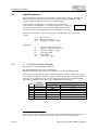
About the Cover Image
The cover image shows a Rev 4 BitsyXb.
Printing this Manual
This manual has been designed for printing on both sides of an 8.5x11 inch paper, but can be
printed single-sided as well. It has also been optimized for use in electronic form with active
cross-reference links for quick access to information.
Revision History
REV
2
3
DESCRIPTION
First preliminary release
Second preliminary release
Sections remaining for update are marked "tbd"
ADS document # 110118-00013, preliminary
BY
10/25/05 ak
11/8/05 ak
Page i
BitsyXb User’s Manual
(This page intentionally blank)
Page ii
ADS document # 110118-00013, preliminary
BitsyXb User’s Manual
Table of Contents
About the Cover Image ..........................................................................................................................................i
Printing this Manual...............................................................................................................................................i
Revision History ....................................................................................................................................................i
Table of Contents .................................................................................................................................................iii
1
2
3
Introduction.......................................................................................................................................1
1.1
Overview ...............................................................................................................................1
1.2
Features..................................................................................................................................1
1.2.1
Processor......................................................................................................................1
1.2.2
Power Supply...............................................................................................................1
1.2.3
Memory .......................................................................................................................1
1.2.4
Communications..........................................................................................................2
1.2.5
User Interface and Display ..........................................................................................2
1.2.6
I/O................................................................................................................................2
1.2.7
Audio Interface ............................................................................................................2
1.3
Block Diagram.......................................................................................................................3
Getting Started ..................................................................................................................................5
2.1
Development Systems ...........................................................................................................5
2.1.1
System Components ....................................................................................................5
2.1.2
BitsyXb Personality Boards.........................................................................................5
ADS CompactFlash Personality Board
ADS Ethernet Personality Board
ADS Quad UART Ethernet Personality Board
2.2
Frequently Asked Questions..................................................................................................6
2.3
Organization of this Manual ..................................................................................................7
2.4
Errata, Addenda and Further Information..............................................................................7
Hardware Reference..........................................................................................................................9
3.1
Switches, Controls and Indicators .........................................................................................9
3.1.1
S1: DIP Switch ...........................................................................................................9
3.1.2
LED Indicator ..............................................................................................................9
3.2
Jumper Settings .....................................................................................................................9
3.2.1
JP2: LCD Display Power Select .................................................................................9
3.3
Signal Connectors................................................................................................................10
3.3.1
J1: LCD Panel Interface Connector ..........................................................................10
3.3.2
J2: PCMCIA .............................................................................................................11
3.3.3
J3: Power, I/O, Serial 2 & 3, USB, Touch Screen and others...................................12
ADS document # 110118-00013, preliminary
Page iii
BitsyXb User’s Manual
3.3.4
3.3.5
3.3.6
3.3.7
3.3.8
3.3.9
3.3.10
4
Page iv
J6: Input Power.........................................................................................................13
J7: XScale I/O Signals ..............................................................................................13
J8: Vee Adapter ........................................................................................................14
J9: External CompactFlash / Expansion Bus ............................................................14
J11: Supercapacitor Input .........................................................................................17
J10: ADSmartIO, USB, Serial 1, Stereo Audio, I/Os ...............................................16
J16: In-System Programming ...................................................................................17
Feature Reference ...........................................................................................................................19
4.1
System Architecture ............................................................................................................19
4.1.1
Boot Code..................................................................................................................19
4.1.2
Synchronous DRAM .................................................................................................19
4.1.3
Non-Volatile Memory ...............................................................................................19
Flash Memory
ADSmartIO EEPROM
CompactFlash and PCMCIA/ATA Cards
RTC NVRAM
4.1.4
Interrupts....................................................................................................................20
4.1.5
CompactFlash / Expansion Bus .................................................................................20
4.1.6
PXA270 GPIO Cross-Reference ...............................................................................20
4.2
Real-Time Clock (RTC) ......................................................................................................23
4.3
ADSmartIO..........................................................................................................................23
4.3.1
Overview ...................................................................................................................23
4.3.2
ADSmartIO Features .................................................................................................24
4.3.3
Digital I/Os ................................................................................................................24
4.3.4
Analog Inputs (A/D) ..................................................................................................24
4.3.5
Temperature Sensing .................................................................................................24
4.3.6
Keypad Scan ..............................................................................................................24
4.3.7
ADSmartIO Signal Cross-Reference .........................................................................26
4.4
Audio ...................................................................................................................................27
4.4.1
Microphone Pre-amps................................................................................................27
4.4.2
Audio Outputs: Speakers and Headphones................................................................27
Connecting Speakers
Connecting Headphones
Using Stereo Headphones and Speakers in the Same System
4.5
Buses and Data Communications ........................................................................................29
4.5.1
Serial Ports.................................................................................................................29
4.5.2
USB ...........................................................................................................................30
USB Host
USB Function (Client)
4.5.3
Synchronous Serial Ports...........................................................................................31
Overview of Synchronous Serial Ports
SSP on the PXA270
SSP on the BitsyXb
4.5.4
I2C Bus Master...........................................................................................................33
I2C on the BitsyXb
4.5.5
Multimedia Card (MMC) Controller .........................................................................33
ADS document # 110118-00013, preliminary
BitsyXb User’s Manual
5
4.6
Displays ...............................................................................................................................34
4.6.1
Display Types Supported...........................................................................................34
4.6.2
LCD Voltages ............................................................................................................34
4.6.3
Display Signals ..........................................................................................................34
4.6.4
Creating Display Cables ............................................................................................34
4.6.5
Developing Display Drivers ......................................................................................34
4.6.6
Brightness Control (Backlight)..................................................................................35
4.6.7
Contrast Control (Vee and Vcon) ..............................................................................35
4.6.8
Touch Panel ...............................................................................................................35
4.7
Discrete IOs .........................................................................................................................36
4.7.1
Digital IOs .................................................................................................................36
4.7.2
Analog Inputs ............................................................................................................36
4.7.3
Analog Outputs (PWM).............................................................................................36
4.8
EMI/RFI and ESD Protection..............................................................................................37
4.8.1
Agency Certifications ................................................................................................37
4.8.2
Protecting the Power Supply Inputs ..........................................................................37
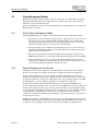
Power and Power Management.......................................................................................................39
5.1
Determining the Features You Need ...................................................................................39
5.2
Power Management Modes .................................................................................................40
5.2.1
XScale Power Management Modes...........................................................................40
5.2.2
Power Management on the BitsyXb ..........................................................................40
5.3
Architectural Overview and Power Management Features .................................................41
5.3.1
Power Supply Architecture........................................................................................41
5.3.2
Subsystem Partitioning ..............................................................................................41
5.3.3
System Sleep .............................................................................................................43
Power Failure Interrupt
RQOnOff Input
Software Control
5.3.4
System Wakeup .........................................................................................................44
RQOnOff Input
Touch Panel
Timed Wakeup
ADSmartIO/Keypad
5.3.5
Supercapacitors..........................................................................................................45
Charging
Discharging
5.3.6
Backlight Power ........................................................................................................46
5.3.7
Battery Trickle Charger (volume production option) ................................................46
5.3.8
Power Supply Efficiency ...........................................................................................47
5.4
Designing for Optimal Power Management ........................................................................47
5.4.1
Create a Power Budget for Peripherals......................................................................47
3.3 V Loads
5 V Loads
Loads on Main Supply
5.4.2
Power Loads During Sleep ........................................................................................48
ADS document # 110118-00013, preliminary
Page v
BitsyXb User’s Manual
5.5
6
7
Page vi
Power Supply Examples ......................................................................................................49
5.5.1
Basic DC Supply .......................................................................................................49
5.5.2
Automotive System ...................................................................................................49
5.5.3
Line Power and Battery with External Charger .........................................................50
System Specifications .....................................................................................................................51
6.1
Mechanical Specifications ...................................................................................................51
6.1.1
Mechanical Drawing..................................................................................................51
6.1.2
Mounting Holes .........................................................................................................51
6.1.3
Clearances..................................................................................................................52
6.1.4
Production Options ....................................................................................................52
Mating Headers on Underside of Board
PCMCIA Rails with no Ejector
Removal of PCMCIA Header
Connector Plating
Microphone Gain
6.2
Electrical Specifications ......................................................................................................53
6.2.1
Temperature, Reset, Sleep, Wakeup ..........................................................................53
6.2.2
LCD Display..............................................................................................................54
6.2.3
Touch Panel Controller..............................................................................................55
6.2.4
Power Supply.............................................................................................................55
6.2.5
Power Consumption ..................................................................................................56
6.2.6
ADSmartIO Controller ..............................................................................................57
6.2.7
System Controller ......................................................................................................58
CompactFlash Port Used as Expansion Bus
6.2.8
Audio .........................................................................................................................59
6.2.9
PXA270 Processor.....................................................................................................60
6.2.10 Crystal Frequencies ...................................................................................................61
Board Revision History...................................................................................................................63
7.1
Identifying the board revision..............................................................................................63
7.2
Revision History ..................................................................................................................63
7.2.1
Revision 4 ..................................................................................................................63
New Features
Changes
ADS document # 110118-00013, preliminary
1
Introduction
1.1
Overview
The BitsyXb is a full-featured single board computer using the PXA270 XScale RISC
microprocessor. The BitsyXb is designed to meet the needs of embedded and graphical systems
developers.
This manual applies to latest revision of the BitsyXb, as listed in the revision history, section 7.2.
1.2
Features
1.2.1
Processor
1.2.2
1.2.3
•
PXA270 32-bit XScale processor
•
Clock rates from 104 to 520 MHz
•
Battery-backed real-time clock
Power Supply
•
6-15 V main power input
•
Battery trickle charger
Memory
1
•
64 MiB synchronous DRAM 1 2
•
32 MiB Flash memory 3
•
PCMCIA, Type I and II, 3.3 and 5 V
•
Supports CompactFlash4 (CF) cards with optional personality board
The BitsyXb supports 16, 32, 64 or 128 MiB SDRAM.
2
MiB is the IEC abbreviation for mebibyte = 220 byte = 1 048 576 byte. The kibi and mebi
prefixes are based on the 1998 IEC standard for binary multiples. For further reading, see the US
NIST web site, http://physics.nist.gov/cuu/Units/binary.html
3
The BitsyXb supports 8, 16, 32 or 64 MiB of synchronous or asynchronous flash. The 64 MiB
flash option is available only in synchronous flash.
4
CompactFlash is a trademark of the CompactFlash Association, http://www.compactflash.org/.
ADS document # 110118-00013, preliminary
Page 1
BitsyXb User’s Manual
1.2.4
1.2.5
1.2.6
1.2.7
Page 2
Communications
•
USB 1.1 Host port (low 1.5 Mbit/s and full 12 Mbit/s speeds) and full speed Client port
•
Three Serial Ports
Serial 1: EIA-232, 3.3V logic level (9-wire)
Serial 2: 3.3V logic level (3-wire); IrDA and EIA-232 with optional personality board
Serial 3: EIA-232, 3.3V logic level (5-wire)
•
10/100BT Ethernet, RJ45 (with optional personality board)
•
CompactFlash Interface (with optional personality board)
User Interface and Display
•
Flat Panel Interface
•
Software-control of external VEE Generator for passive LCD contrast control
•
Analog Touch Panel Interface (four- or five-wire options)
•
External PS/2 Keyboard Support
•
Nine ADSmartIOTM ports configurable for digital I/O, A/D inputs (up to four) and/or up
to 4x5 keypad
•
Ten digital I/Os
•
Backlight Control Signals for Intensity and On/off
•
External Temperature Probe support
I/O
Audio Interface
•
AC'97 Codec
•
Stereo Microphone Input
•
Stereo 1W Speaker Outputs
•
Headphone Output
ADS document # 110118-00013, preliminary
Introduction
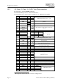
1.3
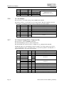
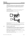
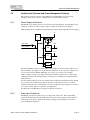
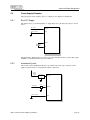
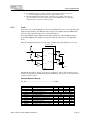
Block Diagram
The following diagram illustrates the system organization of the BitsyXb. Arrows generally
indicate the direction of control and data flow.
The diagram also illustrates a composite of the three Bitsy Personality Boards5. Connectors not
found only on all boards are drawn with dotted lines. See section 2.1.2 for additional details about
the personality boards.
J8
Personality Board
J11
Vee
J6
BitsyXb
supercaps
Power
supply
MMC
Battery
(optional)
J16
Power input
J15
Touch panel
NSSP
J11 USB
Function port
COM1
J3
USB function
J3
J7
J7
Touch panel
controller
SPI
I2C
Battery
charger
J20
buffers
COM2
JP4-7
buffers
COM1
IrDA
digital I/Os
XScale
PXA270
J22
COM2
J36
Wakeup
J12
Backlight
I2C
RTC
LCD
J31
J13
buffers
J1
LCD
J1
+
I2C
SPI
ATMega
J5 P/S2
Keyboard
I/Os
COM3
AC97
Codec
amp
J10
AC97
J44
buffers
J10
SDRAM and
Flash Memory
System Bus
J18
PS/2
COM3
J6
J34
J45
amp
USB host
SW1 Reset
J39 USB
Host port
Quad
UART
CompactFlash
buffers
J9
buffers
J9
System
controller
logic
Ethernet
J46
J47
COM4
COM5
J49
J50
COM6
COM7
Compact
Flash
PCMCIA
J2
J51
J28
5
Personality board connectors cited in the block diagram are from the rev A Ethernet/
CompactFlash personality board and the rev 3 Quad UART personality board.
ADS document # 110118-00013, preliminary
Page 3
BitsyXb User’s Manual
(This page intentionally blank)
Page 4
ADS document # 110118-00013, preliminary
2 Getting Started
2.1
Development Systems
BitsyXb boards are shipped as development systems designed to get the developer up and running
quickly.
To use the system, simply plug power supply into the mini DIN-8 receptacle on the system.
If the screen does not display anything after five to ten seconds, check the Frequently Asked
Questions, below. Most operating systems cold boot within twenty seconds.
2.1.1
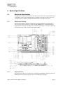
System Components
A typical development system is shown at right. It consists of the
following components:
•
BitsyXb single-board computer
•
Bitsy Personality Board with CompactFlash or 10/100BT
Ethernet
•
Flat panel display and cable
•
Backlight inverter and cable
•
Touch screen and cable
•
120 VAC power adapter
•
Plexiglas mounting
•
Developer's Cable Kit including
•
•
Serial Port DB9 adapter (ADS cable #610111-80001)
•
DB9F/F null modem cable
Operating system of your choice
• User's Guide (this document and operating system guide)
Please make sure you have received all the components before you begin your development.
2.1.2
BitsyXb Personality Boards
The BitsyXb often works in tandem with another board to add functionality and customize the
system for its application. Personality boards can add custom circuits and locate connectors best
suited for the application design.
In production volumes, the BitsyXb can be built with interface connectors J1, J3, J9 and J10 on
the underside of the board. This allows the BitsyXb to rest above custom personality boards rather
than below them. Details about this production option are listed in section 6.1.4.
At the time of writing, ADS supplies a reference design for personality board. Schematics are and
user manuals available on the ADS support site. The following sections describe the type of
boards that are offered at the time of writing.
ADS CompactFlash Personality Board
The CF Personality board breaks out signals from the BitsyXb for a wide range of functions
including USB, audio, keyboard, power, serial, LCD display, backlight, IrDA and touch screen. It
also includes a reset button and CF socket.
ADS document # 110118-00013, preliminary
Page 5
BitsyXb User’s Manual
For further details about this board, please consult the
Personality Board user's manual, ADS document
#110111-8001.
ADS Ethernet Personality Board
The Ethernet Personality Board uses the same circuit
board as the ADS CF Personality Board. An RJ-45 jack
replaces the CF socket, and the board adds an SMSC
LAN91C111 10/100 Ethernet chip and associated line
drivers. Otherwise, the board is identical to the CF
Personality Board.
ADS Quad UART Ethernet Personality Board
The "quad UART" Personality Board removes the CompactFlash socket from the CF/Ethernet
board described above and replaces it with four EIA-232 serial ports. In all other respects, the
board is identical to the ADS Ethernet Personality Board.
2.2
Frequently Asked Questions
The following are some of the most commonly asked questions for development systems:
Q: When I plug in power, my screen is white and nothing comes up on it.
A: Check the connector seating. The flat panel connector may have come loose in shipping.
Press it firmly into the panel and reapply power to your system.
Q: Is there online support?
A: Yes. Information about the BitsyXb hardware and software is available on the ADS support
site at http://www.applieddata.net/support. See section 2.4 for further details.
Q: When I plug in power, my screen stays black.
A: If your system has supercapacitors installed (section 5.3.3), your system may be asleep. Try
waking up the system by shorting the wakeup signal (J3 pin 45) to ground. Development systems
include a two-pin header on the personality board whose pins can be shorted together to wake the
system. You may also press the reset button to fully restart the system.
Q: When I plug in power, the LED doesn't turn on.
A: Your system may still be booting. The LED is software controlled and is not necessarily
turned on at boot.
Q: Do I have to turn off the system before I insert a PCMCIA or CompactFlash card?
A: No. The BitsyXb supports hot-swapping of PCMCIA and CompactFlash cards. Consult the
operating system documentation for details.
Q: Do I need to observe any ESD precautions when working with the system?
A: Yes. If possible, work on a grounded anti-static mat. At a minimum, touch an electrically
grounded object before handling the board or touching any components on the board.
Q: What do I need to start developing my application for the system?
A: You will need a flash ATA card (16 MiB or larger, 32 MiB recommended) and the cables
supplied with your system to interface your development station to the system. For further
direction, consult the ADS guide for the installed operating system.
Page 6
ADS document # 110118-00013, preliminary
Getting Started
Q: Who can I call if I need help developing my application?
A: ADS provides technical support to get your development system running. For customers who
establish a business relationship with ADS, we provide support to develop applications and
drivers.
Q: Can I upgrade the version of the operating system?
A: Yes. ADS provides regular operating system updates on its developers' web site. For
operating systems not maintained by ADS, contact the operating system vendor.
Q: I would like to interface to a different display panel. How can I do this?
A: ADS may have already interfaced to the panel you are interested in. Consult ADS for
availability.
2.3
Organization of this Manual
The manual organizes information in five key sections:
Introduction
Provides an overview of the functionality and organization of the
BitsyXb, as well as how to use this manual.
Hardware Reference
Describes the configuration settings and pinouts for all connectors and
jumpers on the BitsyXb.
Feature Reference
Gives details about the various subsystems of the BitsyXb.
Power Management
Provides key information about power management, tips for system
integration and electrical and mechanical interface specifications.
Specifications
Electrical and mechanical interface specifications.
To locate the information you need, try the following:
2.4
1.
Browse the Table of Contents. Section titles include connector designators and their
function.
2.
Follow cross-references between sections.
3.
View and search this manual in PDF format
Errata, Addenda and Further Information
Errata and addenda to this manual are posted on the ADS support forums along with the latest
release of the manual. Consult the support forums any time you need further information or feel
information in this manual is in error. You may access the forums from the ADS support site,
http://www.AppliedData.net/Support
In addition to manuals, the support forums include downloads, troubleshooting guides, operating
system updates and answers to hundreds of questions about developing applications for ADS
products. You may also post questions you have about ADS products on the forums.
ADS document # 110118-00013, preliminary
Page 7
BitsyXb User’s Manual
(This page intentionally blank)
Page 8
ADS document # 110118-00013, preliminary
3 Hardware Reference
This section gives an overview of the hardware features of the BitsyXb. This overview includes a
description of the switches, jumper settings, connectors and connector pinouts.
Many connectors and headers have a visible number or marking on the board that indicates pin 1.
If that pin is not clearly marked, there are two other ways to locate pin 1:
1.
For through-hole connectors, look at the underside of the board. The square pad is pin 1.
2.
Download the mechanical drawing of the BitsyXb available on the ADS Support site
(section 2.4). The square or indicated pad on each connector is pin 1.
3.1
Switches, Controls and Indicators
3.1.1
S1: DIP Switch
S1 is a two-position DIP switch. When in the "ON" position, switches are closed and connect to
ground. Otherwise they are pulled up.
DIP switch positions "1" and "2" connect to the PXA270.
Most operating systems on the BitsyXb reserve these switches for their use. Consult the operating
system manual for details.
3.1.2
LED Indicator
The BitsyXb has one onboard light-emitting diode (LED) that is turned on and off by the system
controller. The LED is driven by the same buffers as the display driver data lines. The LED will
be off when the display buffers are disabled (see power management section 5.3.2).
3.2
Jumper Settings
There is just one user-selectable jumper on the BitsyXb. It uses a 2mm shorting block (shunt) to
select the setting. Turn off power to the BitsyXb before changing the position of a shunt.
3.2.1
JP2: LCD Display Power Select
Type: 3-post header, 2mm
This jumper selects the supply voltage for the LCD display. The three-pin header is located near
the PCMCIA ejector button.
Jumper setting
Voltage Selected
1-2
Vddx (3.3 V)
2-3
Vcc (5.0 V)
WARNING! Make sure you have selected the correct voltage before connecting the panel. Flat
panels can be irreparably damaged by incorrect voltages.
ADS document # 110118-00013, preliminary
Page 9
BitsyXb User’s Manual
3.3
Signal Connectors
The following tables describe the electrical signals available on the connectors of the BitsyXb.
Each section provides relevant details about the connector including part numbers, mating
connectors, signal descriptions and references to related chapters.
To locate pin 1 of a connector, look for numbers silk screened on the
component side6 of the BitsyXb, or look at the bottom side of a connector for
the square pad, which is pin 1. As seen from the component side, doublerow headers on the board are numbered as shown in the figure to the right.
2 4 6 8...
1 3 5 7...
For information about the location of the connectors on the BitsyXb, refer to section 6.1.1.
Legend:
n/c
GND
(4.1)
Not connected
BitsyXb ground plane
Reference section(s) for signals
I
O
IO
P
A
OC
signal is an input to the system
signal is an output from the system
signal may be input or output
power and ground
analog signal
open collector output
Signal Types
3.3.1
J1: LCD Panel Interface Connector
Board Connector: Samtec #STMM-117-02-T-D
Recommended Mating Cable: Samtec TCSD Series
Recommended Board-to-Board Connector: ESQT series (e.g. ESQT-117-02-F-D-500)
The following table describes the signals on the LCD interface connector. Signal names shown
are for TFT active matrix color LCDs at 16 bpp (bit-per-pixel). For other color depths and LCD
technologies, consult the table in section 4.6.4. Signals from the XScale are buffered and RFI
filtered before reaching J1. See section 4.6 for further details about displays.
Pin
1
2
3
4
5
6
PXA270
Signal Name
L_PCLK
L_LCLK
L_FCLK
Color Active TFT Display at 16bpp
ADS Signal Name
Description
PNL_VEE
VEE (contrast) (3.3.6, 4.6.7)
GND
ground
PNL_PIXCLK
Pixel Clock
PNL_HSYNC
Horizontal Sync.
PNL_VSYNC
Vertical Sync.
GND
ground
6
The "component side" of the BitsyXb is the one on which the PCMCIA ejector is installed. As a
factory option, some connectors may be installed on the "bottom side" of the BitsyXb.
Page 10
ADS document # 110118-00013, preliminary
Hardware Reference
7
8
9
10
11
12
13
14
15
16
17
18
19
20
21
22
23
24
25
26
27
28
29
30
LDD15
LDD11
LDD12
LDD13
LDD14
LDD15
LDD5
LDD6
LDD7
LDD8
LDD9
LDD10
LDD4
LDD0
LDD1
LDD2
LDD3
LDD4
L_BIAS
PNL_RED0
PNL_RED1
PNL_RED2
PNL_RED3
PNL_RED4
PNL_RED5
GND
PNL_GREEN0
PNL_GREEN1
PNL_GREEN2
PNL_GREEN3
PNL_GREEN4
PNL_GREEN5
GND
PNL_BLUE0
PNL_BLUE1
PNL_BLUE2
PNL_BLUE3
PNL_BLUE4
PNL_BLUE5
GND
PNL_LBIAS
Red Bit 0
Red Bit 1
Red Bit 2
Red Bit 3
Red Bit 4
Red Bit 5
ground
Green Bit 0
Green Bit 1
Green Bit 2
Green Bit 3
Green Bit 4
Green Bit 5
ground
Blue Bit 0
Blue Bit 1
Blue Bit 2
Blue Bit 3
Blue Bit 4
Blue Bit 5
ground
Data_Enable
PNL_PWR
Vcc (5 V) or 3.3 V (JP2)
31
PNL_RL
32
PNL_UD
33
ADSmartIO
PD0
34
3.3.2
Horizontal Mode Select
(set by R193 or R207)
Vertical Mode Select
(set by R191 or R192)
PNL_ENA
Panel enable signal
VCON
low-voltage adjust for contrast
control of some displays (6.3.2)
(zero to PNL_PWR volts)
J2: PCMCIA
Integrated ejector: FCI #95620-050CA
The 68-pin PCMCIA socket conforms to the PCMCIA standard for 5V-tolerant Type II cards, and
can also be run at 3.3 V. The socket is normally de-energized; the operating system is responsible
for turning on the socket when a card is inserted and turning it off when the card is removed.
Ejector hardware is standard. A rail-only PCMCIA slot is a volume production option for
installations where clearance is an issue. See section 6.1.4 for details.
Vpp (pins 18 and 52), which is 12 V in older PCMCIA implementations, is left unconnected in
this implementation. See section 6.3.7 for electrical specifications.
ADS document # 110118-00013, preliminary
Page 11
BitsyXb User’s Manual
3.3.3
J3: Power, I/O, Serial 2 & 3, USB, Touch Screen and others
Board Connector : Samtec #STMM-125-02-G-D
Recommended Mating Connector: Samtec # TCSD Series
Recommended Board-to-Board Connector: ESQT series (e.g. ESQT-125-02-F-D-500)
Pin
1
3
Name
EIO9
EIO8
EIO7
GND
VCC
5
7
9
11
13
15
17
19
21
23
25
27
29
31
7
Page 12
Pin
2
4
6
8
10
TEMP_SENSOR
_MINUS
TEMP_SENSOR
_PLUS
/IRDAON
TSPX
TSMY
TSMX
TSPY
EIO5
EIO6
BACKLIGHT
PWM
/BACKLIGHT
ON
RXD2T
TXD2T
WIPER
CHARGE
GND
PE2
CTS3
TXD3
RTS3
RXD3
USB+
USBGND
HP_IN
33
USB_RECONN
35
37
39
43
GND
GND
STXD
SRXD
SCLK2
SFRM2
Type
IO
IO
IO
ground
PO
+5 V
AI
External Temperature Probe Connection
(4.3.5)
12
14
O
AIO
AIO
AIO
AIO
IO
IO
16
AO
18
OC
22
24
26
28
30
32
34
36
PXA270 Digital I/Os (4.7.1, 6.3.9)
P
PO
20
Description
I
O
AI
O
P
O
I
O
O
I
IO
IO
P
I
0
P
P
O
I
O
O
right
top
left
bottom
External IRDA control output
UL
LR
Touch screen
(6.3.3)
LL
UR
PXA270 Digital I/Os (4.7.1, 6.3.9)
Backlight Intensity (PWM)
(4.6.6, 6.3.2)
Backlight On/Off
(open-collector) (4.6.6, 6.3.2)
Serial 2
(3.3 V logic level) (4.5.1)
Touch screen wiper (optional 5-wire touch)
Charge Enable output (PB0 7) (5.3.7)
ground
Power Enable #2 for external devices (5.3.2)
Serial 3
(EIA-232) (4.5.1)
USB Client (4.5.2)
Ground
Headphone connected (4.4.2, 6.3.8)
USB Client power management (4.5.2) 7
connects to ground through R281(0Ω)
ground
MOSI
MISO
SPI signals (4.5.3)
SCLK
SS
This output does not have any series resistance or ESD protection
ADS document # 110118-00013, preliminary
Hardware Reference
Pin
Name
VBATT_POS
VBATT_NEG
41
POWERENABLE
/PE1
DCIN_POS
45
/RQONOFF
47
49
GND
Pin
38
40
42
44
48
Type
PI
P
O
O
PI
I
Description
External Battery Input
(5.3.7)
Power Supply Control Output (5.3.2)
Power Enable #1 for external devices (5.3.2)
External Power Input
(also on J6)
"Request On/Off" Switch Input
(5.3.3, 6.3.1)
46
BATPOS
3.3.4
50
P
ground
PI
Real-time clock backup battery (4.2, 6.3.4)
J6: Input Power
Board Connector: Molex #22-23-2021
Recommended mating connector: Molex 22-01-3027
These power inputs are also connected to J3. See Chapter 5 and section 6.3.3 for input power
specifications.
Pin
1
2
3.3.5
Name
DCIN_POS
GND
Type
PI
P
Description
DC Power Input
Ground
J7: XScale I/O Signals
Board Connector : 2x8, 2mm spacing, Samtec STMM-108-02-G-D-SM
Recommended Board-to-Cable Connector: TCSD series
Recommended Board-to-Board Connector: ESQT series (e.g. ESQT-108-02-F-D-450) 8
This header supplies signals from the XScale that were not available on the StrongARM. These
include I2C and MMC interfaces as well as a number of processor pins that may be used as
general-purpose I/Os (GPIOs) or for alternate, special-purpose functions.
Pin
1
3
4
5
6
7
8
9
10
11
12
Name
I2C_SCA
I2C_SCL
GND
MMCCS0
MMCCS1
MMCMD
MMCDAT0
MMCCLK
MMCCD
VDDX
VCC
Type
IO
IO
P
P
O
O
O
IO
O
I
P
P
Description
I2C (4.5.4)
Ground
Chip select 0
Chip select 1
Command
Card 0 data
Clock
Card Detect
Multimedia Card (MMC)
Controller (4.5.5)
3.3 V
5V
8
Note that the STMM header is 0.050-inch higher than the other 2mm headers on the board
because it is a surface-mount part. Use a correspondingly shorter socket on mating boards.
ADS document # 110118-00013, preliminary
Page 13
BitsyXb User’s Manual
Pin
13
14
15
16
3.3.6
Name
/MMCWP
/MMC_IRQ
/MMCPWREN
MMCDAT1
Type
IO
Description
Write protect
Interrupt
Power enable
Card 1 data
Multimedia Card
(MMC)Controller (4.5.5)
J8: Vee Adapter
Board Connector : 2x4, 2mm spacing, Samtec TMM-104-0-G-D-SM
This header connects to an external Vee power supply adapter. Header J8 supplies power and
control signals to the adapter and receives the Vee output power from the adapter.
Pin
1
2
3
4
5
6
7
8
3.3.7
Name
VCC
VDDX
VEE_CTL
VEE
V_CON
n/c
GND
GND
Type
PO
PO
O
PI
O
P
P
Description
5V
3.3 V
On/off control of Vee power
Vee input to BitsyXb
PWM control of Vee
ground
J9: External CompactFlash / Expansion Bus
Board Connector : Samtec #STMM-125-02-G-D
Recommended Mating Connector: Samtec TCSD Series
Recommended Board-to-Board Connector: ESQT series (e.g. ESQT-125-02-F-D-500)
The BitsyXb makes its CompactFlash bus signals available on J9. These signals can be used to
add a CompactFlash socket to a daughter board or to expand the capabilities of the BitsyXb as a
digital expansion bus. See section 4.1.5 for details.
Pin
1
3
5
7
9
11
13
15
17
19
21
Page 14
Name
GND
/CARDBDET2
/CARDB16
PCBD10
PCBD9
PCBD8
PCBD2
PCBD1
PCBD0
CARDBSTSCHG
CARDBSPK
/CARDBREG
VCC
/CARDBWAIT
CARDBRES
/CARDBVS2
Pin
2
4
6
8
10
Type
P
I
I
IO
IO
IO
IO
IO
IO
I
I
O
PO
I
O
I
Description
ground
Card Detect 2
16 Bit Access
Data8-10
Data0-2
Status Change
Speaker Input
Register Access
5V
Wait
Reset
Voltage Sense 2 Input
ADS document # 110118-00013, preliminary
Hardware Reference
Pin
23
25
27
29
31
33
35
37
39
41
43
45
47
49
Name
PCBA0
PCBA1
PCBA2
PCBA3
PCBA4
PCBA5
PCBA6
+3.3V
/CARDBON
CARDBVCC
CARDBIRQ
/CARDBMWR
/CARDBIOWR
/CARDBIORD
PCBA7
PCBA8
PCBA9
PCBA10
/CARDBMRD
/CARDB_VS1
/CARDBCE2
/CARDBCE1
PCBD15
PCBD14
PCBD13
PCBD12
PCBD11
PCBD7
PCBD6
PCBD5
PCBD4
PCBD3
/CARDBDET1
Pin
12
14
16
18
20
22
24
/CARDBON_3P3V
50
ADS document # 110118-00013, preliminary
26
28
30
32
36
34
38
40
42
44
46
48
Type
O
O
O
O
O
O
O
P0
O
PI
I
O
O
O
O
O
O
O
O
I
O
O
IO
IO
IO
IO
IO
IO
IO
IO
IO
IO
I
O
Description
Address0-6
+3.3 V
5 V Power Control
External Switched CardB Power Input
Interrupt Signal
Memory Write
IO Write
IO Read
Address7-10
Memory Read
Voltage Sense 1 Input
Low Byte Chip Select
High Byte Chip Select
Data11-15
Data3-7
Card Detect 1
3.3 V Power Control
Page 15
BitsyXb User’s Manual
3.3.8
J10: ADSmartIO, USB, Serial 1, Stereo Audio, I/Os
Board Connector : Samtec #STMM-125-02-T-D
Recommended Mating Connector: Samtec # TCSD Series
Recommended Board-to-Board Connector: ESQT series (e.g. ESQT-125-02-F-D-500)
Pin
1
3
5
7
9
11
13
15
17
19
21
23
25
27
29
31
33
9
Name
/EXT_IRQ1
/EXT_IRQ2
EIO4
EIO3
EIO2
EIO1
EIO0
SIGPS2
CLKPS2
USB_PWR_
SENSE
USB_PWR_
CTRL
USB_UDCUSB_UDC+
I2C_SCL
SMTIO1
SMTIO0
SPKR_LSPKR_L+
SPKR_RSPKR_R+
ROW0
ROW1
ROW2
ROW3
ROW4
COL0
COL1
COL2
COL3
RI1
DCD1
DSR1
DTR1
RXD1
TXD1
CTS1
RTS1
Pin
2
4
6
8
Type
I
I
IO
IO
IO
IO
IO
IO
IO
10
I
12
O
14
16
IO
IO
IO
IO
IO
AO
AO
AO
AO
IO
IO
IO
IO
IO
IO
IO
IO
IO
I
I
I
O
I
O
I
O
18
20
22
24
26
28
30
32
34
36
38
40
Description
External Interrupt 1 Input
External Interrupt 2 Input
PXA270 Digital I/Os (4.7.1, 6.3.9)
External PS/2 keyboard inputs
Sense Input from external USB
host power switch (4.5.2)
Discrete output to control external
USB host power switch (4.5.2)
USB Host (4.5.2)
PC6
PD1
PD0
I2C clock 9
Thermistor energize (4.3.5)
Passive panel enable (PNL_ENA)
Stereo Speaker, left channel (4.4.2)
Stereo Speaker, right channel (4.4.2)
PC0
PC1
PC2
PC3
PC4
PA0
PA1
PA2
PA3
ADSmartIO
(see section 6.3.6)
Serial 1 10
(EIA-232 with 3.3 V logic level volume
production option)
(4.5.1)
PC6 and PC7 are used for the I2C bus master interface. See section 4.5.4 for details.
10
Serial 1 signals RTS, CTS, DCD, DTR, DSR and RI are controlled by the PXA270 GPIO lines.
See section 4.1.6 for details.
Page 16
ADS document # 110118-00013, preliminary
Hardware Reference
Pin
35
37
39
41
43
45
47
Name
/EXT_IRQ3
VDDX
MIC_GND
MIC_L
MIC_R
VREF
/RESET_IN
VDDX
VCC
49
3.3.9
Pin
I2C_SDA
GND
42
44
46
48
50
Type
I
PO
Description
External Interrupt 3 Input
3.3 V
P
Microphone ground
AI
AI
AO
I
PO
ADSmartIO A/D reference voltage
External Reset Input (6.3.1)
3.3 V
PO
5V
IO
P
Stereo Microphone Input
PC7
I2C data 9
ground
J11: Supercapacitor Input
Board Connector: B 2B-ZR-SM3-TF
This header provides a connection point for external supercapacitors. See section 5.3.5 for further
details.
Pin
1
2
3.3.10
Name
SUPCAP+
SUPCAP-
Type
PI
PI
Description
positive connection
negative connection
J16: In-System Programming
Board Connector : 2x8, 2mm spacing, Samtec STMM-108-02-G-D-SM [tbd]
This header is used during manufacturing for programming and test, but is not otherwise
supported for application use. Production customers may use this header to reprogram boot code.
Pin
1
2
3
4
5
6
7
8
9
10
11
12
13
14
15
16
Name
/TRST
TMS
GND
TDI
TCLK
VDDX
GND
TDO
/FWE
FRDY
MISO
VCC
SCK
MOSI
PRG
GND
ADS document # 110118-00013, preliminary
Type
I
I
P
I
I
PO
P
O
O
O
O
PO
I
I
I
P
Description
JTAG
ATMega/ADSmartIO
Page 17
BitsyXb User’s Manual
(This page intentionally blank)
Page 18
ADS document # 110118-00013, preliminary
4 Feature Reference
This chapter provides details about the architecture and many features of the BitsyXb, and how
they can fit together to create a system that meets your application needs.
4.1
System Architecture
This section describes the core functionality of the BitsyXb.
4.1.1
Boot Code
The BitsyXb uses the first block of onboard flash to store the boot code. At the factory, boot code
is loaded using the JTAG interface (J16, section 3.3.9). Most ADS BitsyXb boot loaders are
field-upgradeable using a flash card on either the CompactFlash or PCMCIA port.
4.1.2
Synchronous DRAM
The BitsyXb uses synchronous DRAM (SDRAM) for kernel, application and display frame buffer
use. The data bus width is 32 bits. The memory clock speed is one half the CPU core clock
speed. Typical memory bus operation is at 99.5 MHz.
The self-refreshed RAM consumes most of the system sleep current. Sleep current increases
roughly in direct proportion to the amount of RAM installed.
4.1.3
Non-Volatile Memory
There are several ways to store data on the BitsyXb that will survive a power failure. Some
devices can only be accessed through operating system drivers, and not all are available for
application data storage.
Flash Memory
Flash memory is the primary site for non-volatile data storage. The BitsyXb includes flash
memory for non-volatile data storage. The data bus width is 32 bits.
ADS systems store the operating system, applications and system configuration settings in the
onboard flash. Most operating systems configure a portion of the flash as a flash disk, which acts
like a hard disk drive.
ADSmartIO EEPROM
The ADSmartIO controller includes 256 bytes or more of EEPROM storage. ADS reserves a
portion of this memory for future use. Drivers are not yet available for all operating systems.
CompactFlash and PCMCIA/ATA Cards
CF and ATA cards provide removable storage in a wide variety of capacities. These cards can be
cost-effective means to expand system storage capacity for applications that provide access to the
PCMCIA and CF slots. A CF slot must be placed on a daughter board, as it is not included on the
BitsyXb.
ADS document # 110118-00013, preliminary
Page 19
BitsyXb User’s Manual
RTC NVRAM
The real-time clock chip includes 56 bytes of non-volatile RAM. The RAM is maintained as long
as main or backup power is provided to the chip. Drivers are not yet available to access this
feature. Contact ADS Sales if your application requires this feature.
4.1.4
Interrupts
The BitsyXb includes several sources for external interrupts. The following table summarizes the
external interrupt sources and the devices to which they are connected.
Interrupt Signal
Pin
/RqOnOff
J3.45
CARDBIRQ
/EXT_IRQ1
/EXT_IRQ2
/EXT_IRQ3
EIOn
J9.27
J10.1
J10.3
J10.35
J3, J10
IRQ Handler
PXA270, GP 0
(via CPLD)
[tbd]
PXA270, GP 10
PXA270, GP 9
PXA270, GP 1
PXA270
Your operating system may not include drivers for all interrupt sources.
4.1.5
CompactFlash / Expansion Bus
The BitsyXb makes its CompactFlash bus signals available on J9. These signals can be used to
add a CompactFlash socket to a daughter board or to expand the capabilities of the BitsyXb as a
digital expansion bus. The voltage of the bus signals are set by the CardBVcc voltage (3.3 V
or 5 V).
The ADS Bitsy CF and Ethernet Personality Boards use this bus for CF and digital expansion,
respectively. The schematic (ADS document number 640111-8000, available on the ADS Support
Forums) illustrates how to use this bus both ways.
4.1.6
PXA270 GPIO Cross-Reference
The following table describes how the BitsyXb utilizes the XScale GPIO lines (GPn). They are
offered for reference purposes only. Most operating systems make this information transparent to
developers.
GP
0
1
2
3
4
5
6
7
8
9
10
11
12
13
Page 20
Signal Name
Wakeup input
from CPLD
/EXT_IRQ3
Type
Function (connector, section)
I
wakeup from ADSmartIO
I
External interrupt 3 (4.1.4)
I2C_SCL
I2C_SDA
IO
IO
I2C bus
EXT_IRQ2
EXT_IRQ1
tp
CPLD_CLK
tp [tbd]
I
I
External interrupt 2 (4.1.4)
External interrupt 1 (4.1.4)
ADS document # 110118-00013, preliminary
Feature Reference
GP
14
15
Signal Name
tp
CE1 connect
to SDRAM
Type
Function (connector, section)
O
SDRAM chip select
16
17
18
19
20
21
22
23
24
25
26
27
28
29
30
31
32
33
34
35
36
37
38
39
40
41
42
43
44
45
46
47
48
49
50
51
52
53
54
55
56
57
CPU Ready
(CPLD
Interrupt)
IRQ_TP
SCLK-C
SFRM-C
TXD-C
RXD-C
USB_RECON
N
BITCLK
AUDIO_IN
AUDIO_OUT
AUDIO_SYNC
MMCLK
n/c
RXD1
CTS1
DCD1
DSR1
RI1
TXD1
DTR1
TRS1
RXD1
TXD1
CTS3
RTS3
RXD2
TXD2
/POE
/PWE
/PIOR
/PIOW
n/c
n/c
/PCE2
/PREG
/PWAIT
/IOIS16
ADS document # 110118-00013, preliminary
O
I
SSP
AC'97 Codec
O
I
I
I
I
I
O
O
O
I
O
I
O
I
O
Serial 1 (J10, 4.5.1)
Serial 3 (J3, 4.5.1)
Serial 2 (J3, 4.5.1)
PCMCIA/CF Card interface
Page 21
BitsyXb User’s Manual
GP
58
59
60
61
62
63
64
65
66
67
68
69
70
71
72
73
74
75
76
77
78
79
80
81
82
83
84
85
86
87
88
89
90
91
92
93
94
95
96
97
98
99
100
101
102
103
Page 22
Signal Name
LDD0
LDD1
LDD2
LDD3
LDD4
LDD5
LDD6
LDD7
LDD8
LDD9
LDD10
LDD11
LDD12
LDD13
LDD14
LDD15
L_FCLK/VSY
NC
L_LCLK/HSY
NC
L_PCLK
L_BIAS
CS2 [TBD]
CS3?
PSKTSEL
n/c
SSP3TXD
SSP3RXD
SSP3SFRM
SSP3CLK
[tbd] PCMCIA
LDD16
LDD17
USB_PWR_SE
NSE
USB_PWR_C
NTRL
n/c
n/c
MMCDAT0
EIO0
EIO1
EIO2
/MMC_IRQ
n/c
DIP_SW0
n/c
EIO3
EIO4
IRQ_SSP [tbd]
EIO5
Type
O
O
O
O
O
O
O
O
O
O
O
O
O
O
O
O
Function (connector, section)
LCD display (J1)
O
O
O
O
O
CPLD chip select
O
O
O
I
I
ADS document # 110118-00013, preliminary
Feature Reference
GP
104
105
106
107
108
109
110
111
112
113
114
115
116
117
118
4.2
Signal Name
EIO6
EIO7
EIO8
EIO9
DIP_SW1
MMCDAT1
MMCCS0
MMCCS1
MMCMD
RESET_AUDI
O_L
/IRQ_BATT_F
AULT
MMCWP
/MMCCD
n/c
n/c
Type
Function (connector, section)
Real-Time Clock (RTC)
The BitsyXb uses the DS1307 real-time clock chip to maintain the system date and time when the
system is powered down. The operating system typically reads the RTC on boot and wakeup, and
sets the RTC when the system time or date is changed.
The RTC is powered from the BATPOS input. Connect a long-life 3 V battery to the BATPOS
input (J3 pin 50) to maintain the system time.
The system communicates with the RTC on the I2C bus (section 4.5.4). See section 6.3.4 for
electrical specifications.
4.3
ADSmartIO
ADSmartIOTM is a RISC microcontroller on the BitsyXb that is programmed with ADS firmware.
This device provides additional I/O functionality for specialized tasks. Your application software
can configure the standard ADSmartIO for a variety of functions, such as digital I/O, PWM, A/D,
I2C, keypad scan and PS/2 keyboard operation.
4.3.1
Overview
The ADSmartIO controller has four, eight-pin I/O ports named PA, PB, PC and PD. Some of
these ports' pins are used internally, while others are available for user applications. See the signal
cross-reference in section 4.3.7 for details.
Generally, ADSmartIO ports are referenced by port and pin number (e.g. PA2), but I/O signals
may go by several names based on its functionality. See the connector pinouts to cross-reference
ADSmartIO signal names.
Electrical specifications for the ADSmartIO are listed in section 6.3.6. The ADSmartIO
Programmer's Reference (ADS document 110110-4004) gives information about how to use the
ADSmartIO features.
ADS document # 110118-00013, preliminary
Page 23
BitsyXb User’s Manual
4.3.2
ADSmartIO Features
The following are some of the functions that the ADSmartIO can perform. The functions actually
implemented depend on the firmware loaded on your system:
4.3.3
•
General purpose digital I/O and A/D
•
Keypad scan (section 4.3.6)
•
PS/2 keyboard input
•
Backlight on/off and brightness control (section 4.6.6)
•
Contrast control for display (enabled only when pixel clock is running) (section 4.6.7)
•
Read/set real-time clock (RTC) (section 4.2)
•
Wakeup via RQONOFF signal (section 5.3.3)
•
Trickle-charge a battery (section 5.3.7)
•
Read a temperature sensor (section 4.3.5)
•
Monitor system power
•
Reset CPU
Digital I/Os
All available ports on the ADSmartIO controller can be individually configured as inputs or
outputs. If you write a "1" to an I/O port when it is configured as an input, it enables a pull-up
resistor. Electrical specifications are listed in section 6.3.6.
4.3.4
Analog Inputs (A/D)
Each of the Port A I/Os (PA0-PA7) includes an analog-to-digital (A/D) converter. The converters
give full-scale readings when the input voltage is equal to voltage reference Vref
(e.g. V=Vrefreading/1023). Not all ports are available for external A/D use; see section 4.3.7 for
port assignments. Electrical specifications are listed in section 6.3.6.
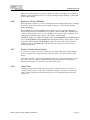
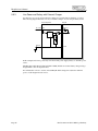
4.3.5
Temperature Sensing
The BitsyXb ADSmartIO can read the temperature of an external
thermistor connected across pins 5 and 7 of J3. The ADSmartIO
controller drives a transistor to energize the thermistor, then reads
the result through the voltage divider created by the thermistor (Rth)
and an internal resistor (Rtl). The thermistor circuit is shown at
right.
Electrical specifications for the temperature sensing circuit are
listed in section 6.3.6.
4.3.6
Vref
PD1
7
J3
PA4
5
Rtl
Rth
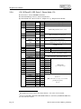
Keypad Scan
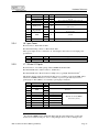
The ADSmartIO can scan a matrix keypad up to four by five keys in size. Matrix keypads are
simpler and cost less than full keyboards and can be easily customized for your application. You
can also create a keypad matrix from a collection of normally-open switches.
When configured to scan a keypad, the ADSmartIO configures the ROWn lines as inputs with
software pull-ups enabled and configures the COLn lines as outputs set to "1"(high). For the scan,
Page 24
ADS document # 110118-00013, preliminary
Feature Reference
the keypad scanner sets successive COLn outputs to "0"(low), then looks for a "0" on one of the
ROWn inputs. The scanner re-reads the pressed key after a delay to debounce the key press.
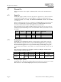
Unused row and column lines can be used for general purpose I/O or A/D.
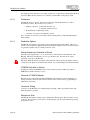
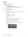
The following diagram illustrates how to connect a 3x3 keypad matrix. The pull-ups are the
software-activated internal resistors of the ADSmartIO, while the series resistors are part of the
BitsyXb.
BitsyXb
ADSmartIO Controller
3 x 3 Keypad
ROW 0
SW1
SW2
SW3
SW4
SW5
SW6
SW7
SW8
SW9
ROW 1
ROW 2
COL 0
COL 1
COL 2
ADS document # 110118-00013, preliminary
Page 25
BitsyXb User’s Manual
4.3.7
ADSmartIO Signal Cross-Reference
The ADSmartIO microcontroller serves many functions in the BitsyXb. The following table
illustrates how the microcontroller ports are utilized for ADSmartIO functionality on the BitsyXb.
Entries in parentheses indicate indirect connections to the listed pin (e.g. through voltage dividers
or additional circuits). Signals with conventional protection circuits are considered directly
connected. I=input, O=output.
PA0
PA1
PA2
PA3
PA4
PA5
PA6
PA7
Pin
J10.27
J10.29
J10.31
J10.33
J3.5
(J3.38)
Type
IO
IO
IO
IO
AI
I
O
AI
PB0
PB1
PB2
PB3
PB4
PB5
PB6
PB7
J3.22
-
O
I
O
O
PC0
PC1
PC2
PC3
PC4
PC5
PC6
PC7
J10.17
J10.19
J10.21
J10.23
J10.25
(J1.3)
(J10.11)
(J10.49)
IO
IO
IO
IO
IO
I
IO
IO
PD0
PD1
PD2
PD3
PD4
PD5
PD6
PD7
J10.15
J10.13
J10.9
J3.45
(J1.1)
(J3.16)
J10.7
(J3.18)
O
O
IO
I
O
O
IO
O
Port
Function
Keypad, A/D or digital I/O
Thermistor reading
DC_GOOD11
Reset CPU
VBATT_POS divided by 7.2
Battery charger
System Power enable
Wake up CPU
IRQ to CPU
SSP_SFRM
SSP RX (MOSI)
SSP communication
with CPU
SSP TX (MISO)
SSP CLK
Keypad, A/D or digital I/O
Pixel clock
unused 12
Passive panel enable (PNL_ENA)
Thermistor energize (4.3.5)
PS/2 Clock
wakeup signal from CPLD
Vee PWM
Backlight PWM
PS/2 Data
Backlight on/off
11
DC_GOOD is an internal digital signal that goes low when the input voltage drops below
Vsleep (6.3.1).
12
PC6 and PC7 can be connected to the I2C bus. See section 4.5.4 for details. These pins can be
reconfigured as digital I/Os for volume production applications.
Page 26
ADS document # 110118-00013, preliminary
Feature Reference
4.4
Audio
The BitsyXb includes an AC'97 codec for stereo audio input and output. Electrical specifications
for the audio system are listed in section 6.3.8.
4.4.1
Microphone Pre-amps
The BitsyXb supports the connection of a stereo electret microphone to the MIC_R and MIC_L
inputs on J10. The audio signals run through pre-amplifiers that low-pass filter and boost the
signal before being passed on to the audio codec.
When connecting external electret microphones to the BitsyXb, use the MIC_GND analog ground
plane for improved signal-to-noise ratio. The BitsyXb includes pull-ups to power electret
microphones.
4.4.2
Audio Outputs: Speakers and Headphones
The BitsyXb audio amplifier supports both differential and single-ended output devices.
Differential (or "bridge") drive delivers greater output power and is suitable for speakers, which
can be wired independently from each other. Single-ended mode is used for devices like
headphones, which have a common ground between output channels.
The HP_IN input (J3.32) determines the output mode of the amplifier: When HP_IN is high, the
audio output drive is single-ended, when HP_IN is low, the output drive is differential. An onboard pull-up normally keeps HP_IN high.
Connecting Speakers
When using the BitsyXb to drive speakers, short the HP_IN signal to ground. This places the
output amplifier in differential mode. Connect speakers to the SPKR_L and SPKR_R outputs on
J10.
Connecting Headphones
Standard headphones use a plug wired as shown at
right. Three rings on the plug provide right and left
channels and a common return. Mono headphones
do not include the center ring.
The mating headphone jacks include spring contacts to make an electrical connection with the
headphone and to mechanically hold the plug in place. Some jacks include a mechanical switch
suitable for use with the HP_IN signal that is activated when a plug is inserted into the jack.
Mono Headphones
You can connect mono headphones directly to the
BitsyXb as shown at right. Keep in mind that the
resulting impedance of the parallel-connected
headphone speakers is half that of a single
headphone speaker. See the audio driver
specifications in section 6.3.8 for details about the
minimum impedance an audio output channel can
drive.
Stereo Headphones
When wiring for stereo headphones, wire blocking
capacitors in series with the BitsyXb SPKR- signals
ADS document # 110118-00013, preliminary
Page 27
BitsyXb User’s Manual
as shown at right. These capacitors block the DC component of the audio signal and complete the
conversion from differential to single-ended output drive. Leave the HP_IN signal pulled high to
enable headphone output.
Select blocking capacitor size based on the lowest frequency your application will need to play
out. Larger capacitors give improved bass response (lower frequency cutoff), but are physically
larger and cost more. The corner frequency for the low-pass filter created by the capacitor and the
headphone speaker is calculated as fo=1/(2πRLC). A 330 uF capacitor into a 32 ohm headphone
speaker will give a low cutoff frequency of 15 Hz. Use electrolytic capacitors rated for at least
6.3 V.
The pull-down resistors shown in the diagram drain any charge that builds up on the headphone
outputs when headphones are not connected. Use 1 kΩ resistors.
Page 28
ADS document # 110118-00013, preliminary
Feature Reference
Using Stereo Headphones and Speakers in the Same System
Some applications use both headphones and
speakers. You can wire the headphone jack to
automatically switch the amplifier to single-ended
mode when a headphone plug is inserted in the jack.
This will disable the drive to any speakers that are
wired into the system.
Most headphone jacks include mechanical switches
that indicate when a headphone plug has been
inserted. The diagram at right shows a circuit that pulls down the HP_IN signal when a
headphone plug is removed.
For this circuit to work reliably in differential mode, the HP_IN signal must remain below VHP_IN
through the largest output voltage swings of SPKR_L. Use of 1 kΩ resistors meets this
requirement.
4.5
Buses and Data Communications
The BitsyXb has several built-in channels for communication with peripheral and peer devices.
These include EIA-232 and logic-level serial, USB host and client ports, SPI bus and I2C.
4.5.1
Serial Ports
The BitsyXb has three XScale serial ports configured as follows:
Port
Serial 1
Serial 2
Serial 3
# signals
9-wire
3-wire
5-wire
Connector
J10
J3
J3
Standard
EIA-232 (9-wire)
3.3 V logic level
EIA-232
Production options
3.3 V logic level
3.3 V logic level
The XScale standard serial ports (Serial 2 and 3) supply two or four signals: Serial 2 uses TX and
RX ("three-wire serial", counting GND), while Serial 3 adds RTS and CTS. Serial 1 uses the
XScale "full-featured serial port," which adds four more signals (DTR, DSR, DCD and RI) to
supply the full complement of modem control signals.
The XScale can configure Serial 2 as an IrDA port. IrDA should be used in conjunction with the
IrDAOn signal (J3), which enables the IrDA transmitter. IrDA transceivers can be panel mounted
or placed on a personality board.
Ports that are configured for 3.3 V logic level operation go directly to the XScale and should be
treated electrically as GPIOs. See section 6.3.9 for electrical specifications.
ADS document # 110118-00013, preliminary
Page 29
BitsyXb User’s Manual
4.5.2
USB
The BitsyXb includes signals for USB 1.1 Host and Client ports. Both the USB Host
(downstream) port and the USB Function ("Client" or upstream) port are managed by the PXA270
processor. The BitsyXb can be configured as a self-powered hub, with one Host and one Client
port.
To create a USB connection, you must wire a standard USB socket as described in the following
sections. For each type of connector, pin numbering is as follows:
Pin
1
2
3
4
USB signal
USB_PWR
USB USB +
GND
USB Host
The BitsyXb USB Host port allows you to connect one USB device to the BitsyXb. USB mouse
and keyboard are the most common client devices, but you can connect any USB function device
that has USB drivers installed on the BitsyXb.
Use a Type A connector for the host signals on J10 pins 14 and 16 (section 3.3.8). The mating
face of such a socket is shown at left. The USB standard also permits directly wiring the USB
signals to the target USB device (e.g. USB mouse). To connect more than one USB client device
to the BitsyXb, use a USB hub.
The USB protocol allows client devices to negotiate the power they need from 100 mA to 500 mA
in 100 mA increments. The BitsyXb supplies 5 V power through the USB_PWR pin. Make sure
to account for power used through USB in your BitsyXb power budget (section 5.4.1). It is
recommended that you use a power switch.
The BitsyXb supports two power control signals on J10. USB_PWR_SENSE is an input that
detects over-current conditions. USB_PWR_CTRL an output that controls power to the USB
port. See the BitsyXb CF Personality Board (ADS p/n 640111-8000) for an example of how to
use these signals. Electrical specifications are in section 6.3.9.
USB Function (Client)
The BitsyXb includes a USB Function (or "Client") port. This interface allows the BitsyXb to
appear as a client device to USB Host devices such as desktop and laptop computers.
The USB Function signals are available on connector J3, pins 29 and 30. Connect these signals to
a USB Function Type B socket (mating face shown at left). The USB standard also permits
directly wiring the USB signals to the host or to a host connector (e.g. USB mouse).
Connecting the USB Function Port
This section describes how to connect the signals to create a fully-functioning USB Function port.
See the ADS Bitsy Personality Board reference designs (section 2.1.2) for examples of how to put
these instructions into practice.
The BitsyXb supports the full USB connection speed (12 Mbit/s). Tie a 1.5 kΩ pull-up to the
USB+ signal to indicate this capability to host hardware.
Page 30
ADS document # 110118-00013, preliminary
Feature Reference
USB_PWR is power supplied from the host computer. Since the BitsyXb is self-powered (not
powered by the USB cable), USB_PWR is not needed as a power input. However, USB_PWR is
useful for sensing when a USB cable is connected and for powering the 1.5kΩ pull-up resistor that
indicate to the host that the device supports 12Mbps.
The USB_RECONN output at J3, pin 33, interrupts power to the 1.5kΩ pull-up, simulating a cable
disconnection to the USB host controller. This signal can be used to force the host to reenumerate the BitsyXb (e.g. after wakeup).
4.5.3
Synchronous Serial Ports
This section gives an overview of how synchronous serial ports (SSP) work and describes how
they are used on the BitsyXb.
Overview of Synchronous Serial Ports
Synchronous serial port standards share the same simple architecture: a clock line, transmit and
receive lines, ground and one or more device selects. Each device on the bus requires its own
select line. Buses may be full or half duplex, clocking data one or both directions at the same
time, respectively. Each standard defines which devices are bus masters and which are slaves.
To clarify direction of the data signals, the SPI bus master transmit line (STXD) is also known as
MOSI (Master Out, Slave In), while its receive line is known as MISO (Master In, Slave Out).
The Slave Select (SS) signal, which enables the slave device's transmitter, is also known as
SFRM2 on the BitsyXb.
SSP on the PXA270
The PXA270 provides three identical synchronous serial ports, each of which features the
following capabilities:
•
Frame sizes from four to 32 bits
•
Sixteen-entry, 32-bit transmit and receive FIFOs
•
Adjustable FIFO threshold interrupts
•
Bit clock speeds from 6.3 kbps to 13Mbps
•
Support for the following protocols:
o
Motorola's SPI (Serial Peripheral Interface)
o
National Semiconductor's Microwire
o
Texas Instruments' SSP (Synchronous Serial Protocol)
o
PSP (a Programmable Serial Protocol)
•
Operation as master or slave
•
Receive-without-transmit operation
•
SSP/PSP Network mode, supporting up to eight time slots
Each of these features is available for use on the BitsyXb.
ADS document # 110118-00013, preliminary
Page 31
BitsyXb User’s Manual
SSP on the BitsyXb
The BitsyXb makes use of the three PXA270 synchronous serial ports as illustrated in the
following diagram.
The BitsyXb uses PXA270 SSP1 to communicate with the ADSmartIO controller. The signals for
SSP1 come out to J16 for factory programming, but are not intended for application use.
The BitsyXb uses SSP2 to communicate with the touch panel controller. Applications can use
SSP3 for control of external peripherals.
The BitsyXb generates the SSP bit clocks from the on-chip 13 MHz clock. It does not support an
external clock input.
Electrical specifications for SSP3 are listed in section 6.3.9. Consult the operating system
references for details about how to use the SSP bus for external devices.
Page 32
ADS document # 110118-00013, preliminary
Feature Reference
4.5.4
I2C Bus Master
I2C (Inter-IC) Bus is a multi-master, "two-wire" synchronous serial bus developed by Philips for
communications between integrated circuits (Ics). The bus master addresses devices using the
data line and provides a synchronous clock for reading and writing devices. Client devices
respond only when queried by the master device. Philips has developed many I2C devices, but
other organizations have adopted I2C as a convenient means for addressing peripherals in a
system.
I2C on the BitsyXb
The BitsyXb uses the XScale processor as the I2C bus controller to communicate with the realtime clock (section 4.2) and the CPU core voltage controller. I2C can also be used to
communicate with external devices.
The following diagram illustrates the I2C architecture on BitsyXb.
Vddx
XScale
J7
SCL
SDA
R135
.2
R27
.1
Voltage
Control
RTC
ADSmartIO
PC6
PC7
R28
J10
R128
SCL
SDA
Z31
.11
I2C_SCL
.49
I2C_SDA
Z11
The BitsyXb XScale I2C signals are available on connectors J7 and J10. Electrical specifications
are listed in section 6.3.9.
The ADSmartIO can emulate an I2C bus master using PC6 as SCL and PC7 as SDA and can be
connected to the I2C bus for backward compatibility with older Bitsy family products. Standard
BitsyXb systems do not connect the ADSmartIO controller to the I2C bus.
4.5.5
Multimedia Card (MMC) Controller
The XScale MMC controller provides a serial interface to MMC cards. The controller supports up
to two cards in either MMC or SPI modes with serial data transfers up to 20 Mbps. The MMC
controller has FIFOs that support Direct Memory Access (DMA) to and from memory.
This interface can also be used to access Secure Digital (SD) Memory Cards and Secure Digital
I/O (SDIO) cards. See Intel Application Note 278533 for details and pitfalls.
Signals for the MMC Controller are brought out to header J7. See the XScale Developer's Manual
for details about how to use the MMC interface.
Drivers for MMC may not be available for all operating systems. Contact ADS for driver
availability for the operating system you are using.
ADS document # 110118-00013, preliminary
Page 33
BitsyXb User’s Manual
4.6
Displays
The BitsyXb uses the integrated XScale display controller to drive liquid crystal displays (LCDs).
Connector J1 supplies the power and data signals needed to drive LCDs, while backlight and
touch panel control signals are located on connector J3.
4.6.1
Display Types Supported
ADS has configured the BitsyXb for a wide variety of display types and sizes. Consult the ADS
support site (section 2.4) for the latest list of displays supported by ADS. If a display isn't on the
list, contact ADS Sales for information about ADS' panel configuration service.
The XScale controller uses system memory for the display frame buffer, and can drive VGA
(640x480) and SVGA (800x600) displays easily. Larger displays will work with the XScale, with
some constraints imposed by the controller architecture. The ADS Support Forums provide
details about the design tradeoffs that are required to support larger displays.13
The BitsyXb can drive LVDS displays using an ADS adapter circuit.
4.6.2
LCD Voltages
The BitsyXb supplies 3.3 V or 5 V power to the LCD display via J1. Select this voltage with JP2
(section 3.2.1). Please observe the cautions listed with the JP2 settings.
4.6.3
Display Signals
XScale display signals LDD0 through LDD15—as well as the pixel clock, vertical sync and
horizontal sync—are all buffered at a factory-set voltage. See section 6.3.2 for full specifications.
The PNL_RL and PNL_UD signals are for active (TFT) displays that support changing the scan
direction. This feature allows the display to be flipped right-to-left (RL) or up-and-down (UD) by
changing the voltage on these signals. See section 6.3.2 for full specifications.
4.6.4
Creating Display Cables
ADS has designed cables for a wide variety of displays. See the list of supported displays on the
ADS support forums. Cable drawings for supported displays are available on request.
While ADS does not provide support to customers to create their own cables, designers with LCD
display experience may be able to design their own. For those that do so, a key point to keep in
mind is that the PXA270 LCD interface maps its display controller pins differently based on LCD
technology and color palette size. Consult the PXA270 User’s Manual for more information.14
4.6.5
Developing Display Drivers
The XScale has a bank of registers that define the timing for displays. In addition, the operating
system must define the region of memory for the frame buffer(s).
13
Currently posted at http://www.applieddata.net/forums/topic.asp?topic_id=580
14
Intel PXA27x Processor Family: Developer's Manual. Order number 280000-001, April 2004.
pp. 7-49 to 7-53.
15
Page 34
Double pixel data (DPD) mode = 1
ADS document # 110118-00013, preliminary
Feature Reference
ADS provides display timings for supported displays on request. For displays not yet supported,
ADS has a panel configuration service to create panel timings and cable drawings. Contact ADS
Sales for further details.
4.6.6
Brightness Control (Backlight)
Most LCD displays include one or more cold-cathode fluorescent lamp (CCFL) tubes to backlight
the displays. Some LCDs, such as passive transflective displays, can be viewed in daylight
without backlighting.
Panel backlights are driven by backlight inverters. These circuits are typically external to the
display and generate the several hundred volts required to drive the CCFL tubes. Backlights can
easily become the greatest source of power consumption in a portable system. Fortunately, most
backlight inverters include control signals to dim and turn off the backlight.
The BitsyXb supplies two signals for backlight control: BacklightPWM (J3.16) and /BacklightOn
(J3.18). BacklightPWM is a filtered PWM signal that supplies an analog output voltage to control
the intensity of the backlight. The /BacklightOn signal is an open-collector output to turn the
backlight on and off. The ADSmartIO controller drives these signals. See section 6.3.2 for
electrical specifications.
4.6.7
Contrast Control (Vee and Vcon)
Vee and Vcon are used to control the contrast of passive panels. Many passive panels require a
positive or negative bias voltage in the range of fifteen to thirty volts to bias the passive LCD
display.
Some displays include a Vee generator and simply require a low-voltage analog signal to control
the contrast. The Vcon output is a PWM-controlled output that can be used for this purpose.
Electrical specifications for Vee and Vcon are listed in section 6.3.2.
4.6.8
Touch Panel
The BitsyXb supports four and five-wire analog resistive touch panels (five-wire control is a
volume production option). Connect the touch panel to the inputs on connector J3. The touch
panel controller can wake the system from sleep (section 5.3.3) Electrical details are listed in
section 6.3.3.
ADS document # 110118-00013, preliminary
Page 35
BitsyXb User’s Manual
4.7
Discrete IOs
This section describes discrete signals on the BitsyXb that can be used for measurement and
control.
4.7.1
Digital IOs
The BitsyXb supplies a number of discrete digital I/Os for application use. These are referred to
as general-purpose digital inputs and outputs (GPIOs), as each discrete digital signal can be
configured as an input or as an output. The PXA270 and ADSmartIO controller drive the GPIOs
on the BitsyXb.
The cross-reference in section 4.1.6 is a complete list of all PXA GPIO ports. Section 4.3.7 lists
the usage of all ADSmartIO ports. Electrical specifications for PXA270 GPIOs are listed in
section 6.3.9, while section 6.3.6 lists ADSmartIO electrical specifications.
The following table lists the number of GPIOs available from each source, the series resistance,
whether the signals include ESD protection, the header number and notes about functions of the
port signals.
#
signals
5
5
5
5
4.7.2
Source
PXA270
PXA270
ADSmartIO
ADSmartIO
Series
Resistance
1 kΩ
1 kΩ
1 kΩ
1 kΩ
ESD
prot.
Y
Y
Y
Y
Header
J3
J10
J10
J10
Usage Notes
EIO5-9
EIO0-4
PC0-4 or ROW0-4
PA0-3 or COL0-3
Analog Inputs
The BitsyXb uses the ADSmartIO controller to perform analog-to-digital (A/D) conversions.
These A/D inputs are typically used for low-speed, uncalibrated applications (e.g. user input,
ballpark voltage measurement, etc) as the noise margins on the BitsyXb A/Ds are not suited for
most instrumentation applications. For precision A/D readings, consider taking averages of
several readings, performing two-point calibrations or using an external A/D converter (e.g. over
SSP).
The following table summarizes the A/D inputs available on the BitsyXb. The Ref column
indicates reference sections for their use.
4.7.3
Range
# lines
Rin
Source
Header
0–2.5 V
up to 4
100 MΩ
ADSmartIO
J3
0-2.5 V
1
100 MΩ
ADSmartIO
J3
Ref
4.3.4,
6.3.6
4.3.4,
6.3.6
Details
PA0-3
Thermistor (PA4)
Analog Outputs (PWM)
The BitsyXb has two filtered, pulse-width-modulated outputs that serve as analog control outputs.
These are used to control LCD backlighting and contrast (sections 4.6.6 and 4.6.7).
Page 36
ADS document # 110118-00013, preliminary
Feature Reference
4.8
EMI/RFI and ESD Protection
The BitsyXb board incorporates a number of industry-leading features that protect it from
electrostatic discharge (ESD) and suppress electromagnetic and radio-frequency interference
(EMI/RFI). Transient voltage suppressors, EMI fences, filters on I/O lines and termination of
high-frequency signals are included standard on all systems. For details, see electrical
specifications for subsystems of interest.
4.8.1
Agency Certifications
Many products using ADS single-board computers have successfully completed FCC and CE
emissions testing as a part of their design cycle. Because ADS supplies only the single-board
computer and not fully integrated systems, ADS cannot provide meaningful system-level
emissions test results.
See the crystal frequencies (section 6.3.10) and electrical specifications for information that may
be helpful during agency certifications.
4.8.2
Protecting the Power Supply Inputs
It is the responsibility of the designer or integrator to provide surge protection on the input power
lines. This is especially important if the power supply wires will be subject to EMI/RFI or ESD.
ADS document # 110118-00013, preliminary
Page 37
BitsyXb User’s Manual
(This page intentionally blank)
Page 38
ADS document # 110118-00013, preliminary
5 Power and Power Management
Power management is especially critical in portable and handheld applications where battery
power is at a premium. The BitsyXb includes advanced power management features, including
the low power XScale CPU, partitioned power distribution and ability to run from several types of
DC power inputs. The BitsyXb can also operate as a conventional single-board computer, taking
advantage of the inherently low power consumption of the system.
This chapter describes the architecture of the BitsyXb power supply, factors affecting power
consumption and reference designs to get you started. For information about how much power the
BitsyXb consumes, consult the electrical specifications in section 6.3.5.
5.1
Determining the Features You Need
System is On All the Time
RTC battery (4.2
nd 5.5.1)
Supercapacitors
(5.3.5)
Battery-Operated, Minimum
Power Consumption
"Pulled-Plug"/Brownout
Protection
Must Preserve Time and Date
Under All Circumstances
ADS document # 110118-00013, preliminary
Battery charging
(5.3.7 and 5.5.3)
System battery
(5.3.1)
Backlight power
control (5.3.6)
System Power Supply Turned
Off to Shut Down System
System Should "Turn Off"
when not in use
Sleep/ wakeup
button (5.3.3)
Features Required
Control ext power
supply (5.3.2)
Relevant Topics
"Line" power
(5.3.1)
Not all designs with the BitsyXb need to be optimized for lowest power consumption. Consider
the following types of typical system configurations to determine the topics of interest to your
application.
Page 39
BitsyXb User’s Manual
5.2
Power Management Modes
Handheld and portable systems available today never really turn "off." They make use of power
management algorithms that cycle the electronics into "standby" and "sleep" modes, but never
fully remove power from the full system.
This section describes the various power management modes of the XScale processor and how the
BitsyXb makes use of them.
5.2.1
XScale Power Management Modes
The XScale PXA270 processor supports four operational modes: Turbo, Run, Idle, and Sleep.
5.2.2
•
Sleep mode uses the least amount of electrical power. The processor core is powered off
and only a few processor peripherals (RTC, I/Os and interrupt control) remain active.
The transition back to Run mode may take a few hundred milliseconds, as clocks must
stabilize and hardware that was powered off must be reinitialized.
•
Idle mode reduces power consumption by pausing the processor core clock. Processor
peripherals remain enabled. This mode is used for brief periods of inactivity and offers a
quick transition back to Run mode.
•
Run mode is the standard mode used when applications are running. It offers the best
MIPS/mW (performance vs. power) performance when running applications from RAM.
•
Turbo mode runs the processor core at up to three times the Run mode speed. Since
external memory fetches are still performed at the memory bus frequency, Turbo mode is
best used when running the application entirely from cache.
Power Management on the BitsyXb
The BitsyXb can actively be configured to be in XScale Run or Sleep modes. Turbo and Idle
modes are controlled by the operating system and are typically transparent to the application.
In Turbo, Run and Idle modes, the power supplies are in their standard, full-power state and
applications run normally on the system. Specific subsystems (as described in section 5.3.2) may
be selectively disabled to conserve power during these states. The operating system is responsible
for adjusting the core voltage (Vddi) for optimal power consumption in each mode.
In Sleep mode, sometimes called "Suspend" mode, the processor puts the SDRAM in a lowpower, self-refresh mode, the processor core shuts off, most peripheral sub-systems are shut down
and the power supplies drop into low-power states or turn off entirely (see the diagram in section
5.3.2 for details). In this state, the BitsyXb consumes very little power, most of which is dedicated
to the maintenance of the RAM (see section 6.3.5 for specifications). The system can be
"awakened" and returned to the Run state by initiating a system wakeup using one of the methods
described in section 5.3.3.
If Main Power (DC_IN or VBATT_POS) drops below the power supply trip point (section 6.3.2),
the BitsyXb automatically goes in Sleep mode. The transition time from Run mode to Sleep mode
is a function of the operating system. System Sleep can also be initiated programmatically.
Page 40
ADS document # 110118-00013, preliminary
Power and Power Management
5.3
Architectural Overview and Power Management Features
This section provides an overview of the architecture of the BitsyXb power supply and a
description of the various features of the BitsyXb power management systems.
5.3.1
Power Supply Architecture
The BitsyXb power supply is laid out as shown in the following diagram. Incoming DC power is
regulated to 5 and 3.3 V. Other system voltages are derived from these power supplies.
[TBD. Diagram shown is for BitsyX. BitsyX changes include external supercaps and Vee supply.]
Vcc
5V
supercaps
Vddi
DCIN_POS
VBATT_POS
Vddi
to CPU core
Vee
Vee
to display
Vddx
3.3 V
switcher
linear
DC_IN and VBATT voltages are mixed using a diode with a low forward voltage. This allows a
battery and DC power supply to be connected at the same time. If only one power supply is used
for your system, use the VBATT_POS input. See sections 5.3.7 and 5.5.3 for examples.
Vddi is a variable-voltage power supply controlled by the XScale I2C bus (4.5.4). This voltage
scaling feature allows the operating system to manage power consumption over the full range of
CPU clock rates.
Several volume production options are available and are indicated by dashed lines in the diagram
above. Options are available for production customers, as described in section 6.1.4, but are
otherwise outside the scope of this manual. Contact your ADS sales representative if you believe
one or more of these options is required for your application.
Specifications for the BitsyXb power supply are listed in section 6.3.4.
5.3.2
Subsystem Partitioning
The BitsyXb can selectively turn off power to subsystems on the board. This load-shedding
feature can extend battery life and significantly increase the amount of time the supercapacitors
will hold up system power. Applications and the operating system determines how selective
power management is utilized.
ADS document # 110118-00013, preliminary
Page 41
BitsyXb User’s Manual
BitsyXb systems that can be selectively disabled include the following:
•
LCD display (panel power and signal buffers)
•
Vee (contrast control)
•
Audio output amplifier
•
Audio codec and microphone pre-amps
•
Serial 1 and 3 EIA-232 buffers
•
External device 1 (/PE1, J3.42)
•
External device 2 (PE2, J3.24)
In addition, the BitsyXb also controls its core power supplies to support sleep operation:
•
Vcc (5 V) supply
• Vddx (3.3 V) Vddi (processor core) supplies
The following diagram illustrates the architecture of the BitsyXb power management system. At
the heart of the system is a power controller that controls the state of the various power
subsystems of the BitsyXb. Under control of the XScale processor, this controller can manage
most of the power distribution of the board. The XScale PowerEnable signal controls the rest of
the subsystems.16
16
The controller inverts the PowerEnable signal for use with some subsystems. This details is not
shown in the diagram.
Page 42
ADS document # 110118-00013, preliminary
Power and Power Management
In the diagram, the power management modes of each of the subsystems are indicated in gray.
Arrows indicate the direction of both signal flow and of power management.
PC Card
Power Management Flow
BitsyXb
ADSmartIO
System
Controller
PCMCIA and CF
RUN
SUSPEND
3.3V
5V
OFF
On/Off
Brightness PWM
Vref
ON
OFF
ON
Backlight Inverter
Vcon
Touch Panel
PXA255 Core
Display Power &
Data Signals
DRAM
LCD Display
ON, OFF
RUN
SUSPEND/SelfRefresh
Flash
Contrast (Vee)
RUN
IDLE
SUSPEND
ON
OFF
PXA255 I/Os
Power Supply, 5V
RUN
BURST MODE
Touch Screen
ON
OFF
READ/WRITE
STANDBY
POWER DOWN
RUN
POWER-DOWN
System
Controller
AC97 Codec &
Mic Pre-amps
ON, OFF
3.3V (Vddx)
RUN: Switcher
SUSPEND: Linear
Audio Amplifier
ON
ON
POWER-DOWN
Core Voltage
ON
OFF
RS-232 Buffers
ON
POWER-DOWN
J3
/CONN_PE1
CONN_PE2
RqOnOff
PowerEnable
5.3.3
System Sleep
This section describes several methods for putting the system into Sleep mode.
Power Failure Interrupt
When the input voltage falls below Vsleep (section 6.3.2), the system generates a in internal power
failure interrupt (the DC_GOOD signal goes low). This interrupt gives the operating system early
ADS document # 110118-00013, preliminary
Page 43
BitsyXb User’s Manual
warning of an impending power failure, allowing the system to drop into low-power Sleep mode
before power has failed completely.
Systems that have supercapacitors benefit from this feature by going to sleep before they begin
drawing down energy stored in the capacitors. This prolongs the amount of time the system can
maintain the contents of RAM.
Operating systems may allow the option to ignore power-failure interrupts. This allows systems to
run with lower input voltages without going to sleep. However, note that if the system does go to
sleep, it will not be able to wake until the input voltage is above Vsleep (see section 5.3.4 for
details).
RQOnOff Input
Operating systems and applications can configure the /RQONOFF signal (J3.45) to put the system
to sleep. In conjunction with the wakeup function (section 5.3.4, below), the RQONOFF input
can be used as an "on/off" button for some systems. Electrical specifications are listed in section
6.3.7.
Software Control
Applications can put the system to sleep programmatically. Operating systems may also put the
system to sleep if the system has not been used for a certain amount of time or for other reasons.
In remote, battery-powered applications, software Sleep can be used in conjunction with the
Timed Wakeup feature (section 5.3.4) for minimum power consumption.
5.3.4
System Wakeup
This section describes several mechanisms for waking a BitsyXb system from Sleep mode. The
system will resume operation in Run mode unless the power supply voltage is lower than Vsleep
(section 6.3.1). If the input voltage is too low, the system will not wake under any circumstances.
This protects the RAM from getting corrupted by an undervoltage condition.
RQOnOff Input
Shorting the /RQONOFF signal (J3.45) to ground will wake the system. The signal is connected
to the system controller. Electrical specifications are listed in section 6.3.7.
Touch Panel
The touch panel controller interrupts the processor when touch panel events occur. Before going
to sleep, the processor can place the controller in a low-power sleep mode from which the
controller generates a wakeup interrupt when a touch event occurs.
Timed Wakeup
The XScale can wake up at a predetermined time. This feature is controlled by software.
ADSmartIO/Keypad
The ADSmartIO controller controls the wakeup signal to the XScale. For production applications,
ADS can configure the ADSmartIO to wake up the system on specific events (e.g. the BitsyXb
adds a volume production option to wake upon keypad activity). Contact ADS Sales if your
application requires a special wakeup event.
Page 44
ADS document # 110118-00013, preliminary
Power and Power Management
5.3.5
Supercapacitors
Supercapacitors (sometimes known as "ultracapacitors") are energy storage devices that combine
the quick charge/discharge characteristics of capacitors with the higher energy density of batteries.
"Supercaps," as they are called, are useful for maintaining power when changing batteries or for
riding out power failures.
The BitsyXb supports connection of external supercaps via header J11.
Charging
There are two important factors related to the charging phase of the capacitors. The first is how
long it takes to fully charge the capacitors. The second is the added load on the power supply it
takes to charge the capacitors. Both are important to effectively use the supercaps.
Charge time for capacitive circuits is typically measured in "time constants," the product of the
charging resistance, R and the capacitance, C. It takes three time constants (3RC) to charge fullydischarged supercaps to 95% of their target voltage. For example, a system with 44 ohm charging
impedance and 1.65 F supercaps has a time constant of 73 seconds. Allow at least five minutes to
recharge the capacitors after the board has been disconnected from power. Charge time is shorter
if the supercaps aren't completely discharged.
The charging current for the supercaps starts out high and diminishes exponentially as the
capacitors reach full charge. Make sure to account for this current in your power budget (section
5.4.1). The charge current is calculated as
i(t) =
Vt - Vi - t/RC
e
R
where
Vt
Vi
t
is the charging/final voltage of the capacitor (assume 5.0 V unless the capacitor
is not charged completely),
is the initial charge voltage of the capacitor, and
is the time in seconds
Use the maximum current (time=0, Vi=0, i(0)=imax=Vt/R) in your power budget.
Discharging
When power fails on a system equipped with supercaps, the operating system shuts off all power
to the board and puts the system to sleep. When power is restored, the system remains asleep until
either the system is awakened (J3.45) or is reset (J10.45).
The amount of time that a system can remain asleep using only supercap power depends primarily
on how quickly external power drops off and how quickly the operating system can put the board
to sleep.
If the operating system can shut down the system before the power supply drops below the
supercap charge level, you will get significantly longer sleep time from your supercaps. You can
calculate how much time the system will have to go to sleep based on (1) how quickly your power
supply will fall when main power fails and (2) the trip point of the BitsyXb power fail circuit
(section 6.3.1). When possible, put the system to sleep with software if a power failure condition
is expected (e.g. changing a battery).
ADS document # 110118-00013, preliminary
Page 45
BitsyXb User’s Manual
The supercaps discharge linearly from the constant-current drain during sleep according to the
equation
t=
(Vi - Vf - 0.2) * C * Eff
I sleep
where
t
Vi
Vf
C
Eff
Isleep
is the duration the system can sleep, in seconds;
is the initial charge voltage of the capacitor;
is the supercap voltage at which onboard systems will fail (assume 3.2 V);
is the capacitance of the supercaps, in Farads;
is the efficiency of power delivery; 85-90% is a safe value to use;
is the amount of current the system consumes while in sleep mode.
For example, a system with fully charged 1.65 F supercaps and a sleep current of 4 mA can expect
to run for up to ten minutes after a power failure. Consult the electrical specifications of section
6.3.4 and power consumption specifications of 6.3.5 for the values to use in your calculations.
5.3.6
Backlight Power
The BitsyXb provides software control of Backlight Intensity and On/Off using the ADSmartIO
controller. Power for the backlight is not routed through the board, and must be supplied to the
backlight separately from the BitsyXb. This provides the greater flexibility when selecting
backlight inverters for an application. See section 4.6.6 for further details about backlight control.
5.3.7
Battery Trickle Charger (volume production option)
The BitsyXb includes a trickle charger for basic charging of external batteries. The following
diagram illustrates the charging circuit and a standard means of combining it with DC line power.
BitsyXb
DC "Line"
power
DCIn_Pos
VBatt_Pos
VBatt_Neg
Charge
Ground
Ground
The Charge signal comes from the ADSmartIO controller (port PB0) and is also available on J3
pin 22 for external use. Writing a logic "1" to PB0 turns on the trickle charging. It is up to the
application to manage battery charging.
Page 46
ADS document # 110118-00013, preliminary
Power and Power Management
The diode on the negative terminal of the battery allows the battery to power the BitsyXb at any
time, but prevents the battery from being charged by a DC voltage on the DCIN_Pos input. The
charge current is calculated as follows:
Icharge =
DCIN_Pos - (2 ∗ 0.2) - Vbatt
R
where
Vbatt is the battery voltage (Vbatt_pos-Vbatt_neg), and
R is the charge resistor (section 6.3.4).
While standard systems include the charging circuit, the charge resistors must be selected for
effective charging of specific batteries to be used. Select a resistor value that will provide the
desired charge current but not exceed the power rating of the resistor. Since P=I2R,
Icharge, max =
Pch / R
where Pch is the maximum power the charge resistor can support. Consult the electrical
specifications in section 6.3.4 for the values populated on standard systems.
5.3.8
Power Supply Efficiency
The BitsyXb power supply achieves high efficiency through several means. First, it utilizes highefficiency switching regulators. These regulators use conventional step-down switchers under
operating load conditions, but are configured by the system for linear and "burst" mode17 operation
during low-load conditions that occur during system sleep. Additionally, there is only one level of
cascaded regulation, reducing the losses that multiply through each stage.
5.4
Designing for Optimal Power Management
Designing a system for optimal power management requires careful attention to many details.
This section provides some guidelines and tips for best power management.
5.4.1
Create a Power Budget for Peripherals
Embedded system designers using the BitsyXb should have a clear understanding of how power
usage will be allocated in the system they design. Designers should create a power budget that
takes into account the types of devices that are expected to be used with the BitsyXb.
The following lists detail some of the typical external loads that can be placed the BitsyXb power
supplies. Baseline power consumption of the BitsyXb is listed in section 6.3.5.
3.3 V Loads
Typical external loads on the 3.3 V power supply include the following:
17
•
Display
•
Personality Board
•
CF and some PCMCIA cards
"Burst mode" in this context is a registered trademark of Linear Technology Corporation
ADS document # 110118-00013, preliminary
Page 47
BitsyXb User’s Manual
5 V Loads
5 V loads come from both onboard and external devices:
External:
• Display
•
Backlight
Only if powered by 5 V BitsyXb power supply
•
Most PCMCIA cards
•
USB devices
•
PS/2 keyboard
Speaker(s)
Assume 80% efficiency
Onboard:
• 3.3 V Supply
Multiply by 115% to account for 3.3 V power supply efficiency
•
•
Supercaps
Use peak inrush current in your budget
Loads on Main Supply
The main power supply (DCIN_Pos or Vbatt_Pos) is loaded by the 5 V and 3.3 V supplies as
indicated in the diagram of section 5.3.1. Assume 85% efficiency for external loads that cascade
through the 5 V supply. Consider these loads when creating your power budget.
5.4.2
Power Loads During Sleep
When designing systems for minimal power consumption during Sleep mode, make sure to
consider DC losses to external connections. The following are a few of the ways your system may
"leak" when asleep:
Page 48
•
PCMCIA and CF cards
Cards in place when the system is asleep can drain power through the Card Detect and
Voltage Sense lines. Assume that all four lines ground the BitsyXb PCMCIA pull-ups
while the card is inserted.
•
Digital I/Os
Review digital I/O connections for potential voltage differences from external
connections when the BitsyXb is asleep.
•
USB
Depending on how USB devices are powered and how the operating system handles
USB, USB devices may draw power during Sleep.
ADS document # 110118-00013, preliminary
Power and Power Management
5.5
Power Supply Examples
The following are basic examples of how to configure power supplies for the BitsyXb.
5.5.1
Basic DC Supply
The simplest way to power the BitsyXb is to supply DC power to the Vbatt_Pos input, as shown
below.
DC power
VBatt_Pos
System ground
Ground
BATPOS
+
GND
This diagram also illustrates how to connect a coin cell to the RTC circuit for systems that require
the RTC to be maintained under all power conditions.
5.5.2
Automotive System
This system connects the BitsyXb directly to the vehicle battery, but polls a sense line on the
ignition to put the system to sleep when the vehicle is turned off.
Vehicle
battery
(~12V)
12V ignition
Vehicle ground
ADS document # 110118-00013, preliminary
Transient/spike
suppression
VBatt_Pos
8V trip
0-3.3V
digital input
Ground
Page 49
BitsyXb User’s Manual
5.5.3
Line Power and Battery with External Charger
You may choose to use an off-board battery charger for a specific battery chemistry or voltage.
The following diagram illustrates one way to include a charger on your own personality board.
Personality Board
BitsyXb
DCIN_Pos
DC "Line" power
Charger
VBatt_Pos
Ground
Ground
In this example, DC "Line" power may come from a DC power supply, battery or other DC power
source.
The Bitsy Personality Board (ADS p/n 640111-8000) includes an external battery charger using a
design similar to the one depicted above.
For an illustration of how to use the onboard BitsyXb trickle charger in conjunction with line
power, see the diagram in section 5.3.7.
Page 50
ADS document # 110118-00013, preliminary
6 System Specifications
6.1
Mechanical Specifications
The BitsyXb is 3.0 inches by 5.0 inches in size. This section describes the component dimensions
and mounting of the board. Detailed drawings are available on the support forums (section 2.4),
and 3D models are available from ADS in electronic format for production customers.
6.1.1
Mechanical Drawing
The following mechanical drawing of the BitsyXb specifies the dimensions of the BitsyXb, as
well as locations of key components on the board. The PCMCIA ejector is integrated into the
design and is not removable. All dimensions are in inches. This image is an excerpt from the full
mechanical drawings, ADS document number 630118-00004.
6.1.2
Mounting Holes
Four holes are provided, one on each corner, for mounting. The diameter of the holes is 0.138-in.
Mounting holes are plated through and connected to the BitsyXb ground plane.
ADS document # 110118-00013, preliminary
Page 51
BitsyXb User’s Manual
For reliable ground connections, use locking washers (star or split) when securing a BitsyXb in an
enclosure. Make sure that washers do not extend beyond the limits of the pads provided.
6.1.3
Clearances
The BitsyXb has a low profile. It can fit in an enclosure with inside dimensions as thin as
0.759 inch (19.3 mm). Key clearances are as follows:
•
Highest component: 0.425 inch (10.8 mm), top
0.172 inch (4.4 mm), bottom
•
Board thickness: 0.062 inch (1.6 mm)
• Clearance over top/bottom: 0.05 inch (1.3 mm)
Note: Selection of connectors, personality board and wiring harnesses will determine height of
final assembly.
6.1.4
Production Options
The BitsyXb has a number of production options detailed throughout this manual. This section
describes options that most significantly affect the mechanical design of the board. These options
are generally available only for volume production orders.
Mating Headers on Underside of Board
The four system signal headers—J1, J3, J9 and J10—can be mounted on the underside of the
BitsyXb. This allows the BitsyXb to sit on top of another board. Note that J7 can only be
populated on top side of the BitsyXb.
Important! When the headers are placed on the underside of the board, the pin numbers will not
correspond to the signals as described in this manual. Lay out the mating board with this in mind.
PCMCIA Rails with no Ejector
In applications where the PCMCIA ejector causes clearance problems, ADS can populate a
PCMCIA slot that has rails but no ejector.
Removal of PCMCIA Header
BitsyXb systems can be built without the PCMCIA header, which can result in significant cost
savings. The base, surface-mount connector remains on the board for factory programming at
ADS and at your facility.
Connector Plating
Connectors on the BitsyXb come standard with gold plating. ADS can populate headers with
different platings as required.
Microphone Gain
The BitsyXb microphone circuitry can be configured for different gain. The most likely reason is
to support "line in" inputs (1 Vrms with no electret pull-ups), but other gain and filtering settings
are possible as well.
Page 52
ADS document # 110118-00013, preliminary
System Specifications
6.2
Environmental Specifications
The following are environmental specifications for the BitsyXb single-board computer.
Symbol
Parameter
Operating temperature
6.3
Min
Typ.
-40
Max
+85
Units
°C
Electrical Specifications
This section provides electrical specifications for the BitsyXb single-board computer.
6.3.1
Reset, Sleep, Wakeup
Absolute Maximum Ratings
Reset Input (RESET_IN)............................. 3.6 V (note 1)
Wakeup Input (/RqOnOff) ........................... 5.5 V (note2)
Symbol
Reset_In (J10.45)
Vrst
Vprst
Rprst
Sleep (5.3.3)
Vsleep
Parameter
Min
trigger voltage (Note 3)
pull-up voltage
pull-up resistance
Sleep trigger voltage (Note 4)
Sleep trigger release hysteresis
(Note 5)
Wakeup: RqOnOff (J3.45)
trq
wakeup pulse duration (Note 6)
Vprq
pull-up voltage
Rprq
pull-up resistance
Vsleep,hyst
Typ.
Max
Units
2.7
Vddx
47
V
V
kΩ
5.4
5.8
V
0.06
0.25
V
100
Vddx
11
ms
V
kΩ
Notes:
1.
The reset controller can support operating voltages up to 10 VDC. However, such high
voltages on Vddx through the pull-up resistor may damage the system.
2.
The RqOnOff signal is connected to the system controller, which determines this rating
(see section 6.3.7).
3.
Short /Reset_In to GND to reset system
4.
This is the voltage at VBATT_POS at which the DC_GOOD signal (4.3.7) changes from
high to low, which can trigger the system to go into Sleep mode. Sleep trigger at
DCIN_POS is Vsleep+Vdin (6.3.4).
Important! Once Vsleep has been triggered, the input voltage must rise at least
Vsleep,hyst above Vsleep before the voltage detector will restore the DC_GOOD signal.
Make sure that your input voltage is designed to always run above Vsleep+Vsleep,hyst, or
systems that go to sleep may not be able to wake again.
5.
6.
Short /RqOnOff to GND to for at least trq to wake up system. A low-level voltage on
/RqOnOff initiates wakeup.
ADS document # 110118-00013, preliminary
Page 53
BitsyXb User’s Manual
6.3.2
LCD Display
LCD display panels have a wide range of voltage and data requirements. The BitsyXb has a
number of adjustable voltages to support these requirements, as well as controls for brightness
(backlight) and contrast (passive LCD panels). See section 4.5.5 for further details.
Symbol
Parameter
LCD (4.6.2)
V pnl
Display power supply (note 7)
P pnl_pwr
Display power (note 8)
V pnl_data
Panel data voltage (note 9)
Scan direction (active displays) (4.6.3)
R pnl_rl
Pull-up/down resistance
R pnl_ud
Pull-up/down resistance
V pnl_rl
(note 10)
V pnl_ud
(note 11)
Contrast Control (passive LCD displays) (4.6.7)
Vcon
Low-voltage contrast adjust (note 12)
Brightness Control (backlight, 4.6.6)
V backlightOn
(note 13)
V backlightPWM
PWM (note 14)
R backlightPWM PWM series resistance (note 14)
Min
Typ.
Max
Units
3.3
3.3
5.0
2
5.0
V
W
V
0
0
4.7
4.7
V pnl
V pnl
V pnl
V pnl
kΩ
kΩ
V
V
0
Vddx
V
0
30
3.3
V
V
kΩ
3.3
1.2
Notes:
7.
JP2 selects the display voltage.
8.
Total power available depends on system power budget.
9.
Systems are configured at the factory with buffers for 3.3 or 5 V panel data. R148 selects
5 V power for the buffers while R137 selects 3.3 V power. 5 V displays with
Vih <= 0.6Vpnl_pwr (3.0 V) will work reliably with 3.3 V data.
10. PNL_RL is pulled up with R193 or pulled down with R207.
11. PNL_UD is pulled up with R191 or pulled down with R192.
12. Vcon is the low-voltage PWM signal used to control Vee. It can be used directly with some
passive displays to control contrast.
13. BacklightOn is an open-collector output. Most backlight inverters include pull-up resistors
on their on/off inputs. The maximum voltage shown is the rating of the BitsyXb output
transistor.
14. The backlight on/off and PWM outputs are driven by the ADSmartIO controller
Page 54
ADS document # 110118-00013, preliminary
System Specifications
6.3.3
Touch Panel Controller
The BitsyXb uses touch panel controllers from Burr Brown. It uses the ADS7846 to support fourwire analog-resistive touch panels and the ADS7845 to support five-wire panels. The system is
factory-configured for use with four-wire panels. All touch-panel signals are ESD and RF
protected. The touch panel controller is powered during sleep mode and can generate an interrupt
to wake the system.
Symbol
Vdd
---
6.3.4
Parameter
Min
Supply voltage
A/D sample resolution
Typ.
Max
Units
Vddx
12
V
bit
Power Supply
Absolute Maximum Ratings
Supply Voltage (DCIN_POS) .....................................18 V
Symbol
Parameter
Min
System Power
VBATT_POS
BitsyXb supply voltage (Note 15)
Diode drop from DCIN_POS to
VBATT_POS at 130 mA
VDDI
Processor core voltage (6.3.9)
Run
VDDX
3.3 V onboard supply
Sleep
VCC
5.0 V onboard supply
5 V available for display,
Run
I (Vcc)
PCMCIA, USB, J9.15,
Sleep
J10.48, etc. (Note 16)
3.3 V available for
Run
I (Vddx)
display, PCMCIA, J9.23,
Sleep
J10.47, etc. (Note 17)
RTC Backup Power (4.2)
V BATPOS
real-time clock battery backup
I BATPOS
RTC current (note 18)
Battery Trickle Charger (section 5.3.7)
Rch
Charger series resistance
Pch
Charge resistor power rating
5
Vdin
0.85
3.1
4.75
2.2
Typ.
Max
Units
12
15
V
0.35
0.4
V
1.0
3.3
3.15
5.0
1.3
3.5
5.25
V
V
V
V
500
mA
700
mA
100
mA
3.6
500
V
nA
0.25
Ω
W
3.0
300
37.5
Notes:
15. The system can operate down to the minimum voltage shown, but the DC_GOOD signal
may cause the system to go to sleep when running at that voltage. See Power Failure
Interrupt in section 5.3.3 for details. The power failure feature can be overridden.
16. LTC 1771 "Burst" mode, used when the BitsyXb is in Sleep mode, is more efficient at low
currents. However, it is electrically noisier and can cause significantly greater EMI/RFI at
higher current draws.
17. During Sleep mode, Vddx is powered by a linear regulator, which draws from the 5V
supply.
18. Vddx=0V, Vbatpos=3.2 V (source: DS1307 data sheet)
ADS document # 110118-00013, preliminary
Page 55
BitsyXb User’s Manual
6.3.5
Power Consumption
The following table lists typical power consumption for the BitsyXb with varying input voltage
and activity levels. Run mode efficiency of the power supply decreases slightly with higher input
voltage.
Power consumption varies based on peripheral connections, components populated on the system
and the LCD panel connected. Input voltage, temperature and the level of processor activity
affect power consumption to a lesser extent. The measurements are accurate to ± 5-10%.
LCD displays and backlights add significantly to the total power consumption of a system. ADS
Development systems include the Sharp LQ64D343 5V TFT VGA display, which draws about
one watt, and the Taiyo-Yuden LS520 backlight inverter, which draws about six watts at full
intensity.
VBATT_POS
Test Condition
Sleep mode
CPU idle (note 19)
Run mode, max (note 20)
Units
6.5 V
5
85
260
mA
33
550
1690
mW
9V
4
66
190
mA
12 V
36
590
1710
mW
3
52
175
mA
15 V
36
620
2100
mW
3
44
140
mA
45
660
2100
mW
Notes: Power consumption was measured on fully-populated 64 MiB rev 3 BitsyXb system with no peripheral
connections and the following additional conditions:
19. System in Run mode at 104 MHz. Running Linux, the system is predominantly in Idle
mode (<5% CPU utilization).
20. System in Run mode at 520 MHz, running Linux. Full (95-100%) processor utilization
achieved by running multiple instances of a graphics-intensive application.
Page 56
ADS document # 110118-00013, preliminary
System Specifications
6.3.6
ADSmartIO Controller
The ADSmartIO Controller is a second RISC microcontroller on the BitsyXb designed to handle
I/O functions autonomously. The BitsyXb communicates with the ADSmartIO controller using
the PXA270 SPI bus. On the BitsyXb, ADSmartIO is implemented with the Atmel
ATMEGA8535 microcontroller, which has 512 bytes EEPROM.
Absolute Maximum Ratings
Input voltage, any pin ................................................3.8 V
Symbol
Parameter
Vdd
ADSmartIO supply voltage
Rs
Series resistance (note 21)
Vprot
(note 21)
Digital Outputs (4.3.3)
Vol
Voh
I sink
(see notes 21, 22)
I source
(see notes 21, 22)
Digital Inputs (4.3.3)
Vih
Vil
Software-selectable pull-ups to 3.3 V
R
(see note 23)
A/D Inputs (4.3.4)
n
resolution (note 24)
Rin
Vref
A/D reference voltage (note 25)
Ivref
Current drain from ref voltage
Vin
valid A/D input voltage range
I (Vref)
J10.43
Temperature Sensing (4.3.5)
Rth
external thermistor resistance @ 25C
Vt
thermistor excitation voltage
Rtl
lower voltage divider
I2C Bus (4.5.4, note 26)
Bus clock
input buffer size
packet size
Vi/o
I/O voltages
Rbus
pull-up on SDA, SCK
Vbus
Min
Typ.
Max
Units
3.3
1
V
kΩ
V
0.5
2.3
20
12
V
V
mA
mA
0.3
Vdd
Vdd
120
kΩ
10
bit
MΩ
V
uA
V
µA
3.3
0.6
35
8
100
2.5
100
Vref
100
0
33
Vref
47
kΩ
V
kΩ
50
kHz
byte
byte
V
kΩ
V
32
32
see digital I/Os, above
4.7
3.3
Notes:
21. Row and column I/Os have series resistance and overvoltage protection to ground. The
series resistance limits the dc current that any one pin can source or sink.
22. SMTIO0-3 are directly connected to I/O controller without external protection.
23. Control pull-up resistors by writing to bits of IO port when the port is configured as a digital
input (bit mask 1=enable, 0=disable).
24. Digital noise on the board may degrade analog performance under some conditions.
25. Vref turns off when the system is in Sleep mode (section 5.3.2).
26. Specifications based on ADSmartIO release 1010 rev 2 (ADS release #700114-10102)
ADS document # 110118-00013, preliminary
Page 57
BitsyXb User’s Manual
6.3.7
System Controller
A Xilinx XC3128 CPLD on the BitsyXb manages the RqOnOff, CONN_PE1/PE2 (5.3.2) and
other system control signals. It is programmed at the factory using the JTAG interface (3.3.9).
The system controller CPLD also manages the PCMCIA and CompactFlash ports. Specifications
are listed separately, below.
Absolute Maximum Ratings
Input voltage, digital I/O pins......................... -0.5 to 5.5 V
Output current, continuous,
digital I/O pins .......................................... -100 to 100 mA
Symbol
Parameter
Vdd
Digital Outputs
Vol
Voh
Digital Inputs
Vil
Vih
Supply voltage
Min
Typ.
Max
3.3
Units
V
0
2.4
0.4
V
V
0
2.0
0.8
3.5
V
V
CompactFlash Port Used as Expansion Bus
The CompactFlash bus can be used as a digital expansion port on the BitsyXb. The following are
specifications for the CF port used as an expansion bus. [specs tbd]
Symbol
VPCMCIA
I 3.3V
I 5V
Rp pcmcia
Vp pcmcia
Parameter
CARDBVcc: CF port voltage
(note 27)
3.3 V socket current
5 V socket current
Card detect (1 & 2) and voltage
sense (VS1 & 2) pull-ups (note 27)
Card detect and voltage sense pullup voltage (note 29)
Min
Typ.
Max
3.3
5.0
5.0
V
tbd
2
2
W
W
100
Vddx
Digital Outputs
Vol
Voh
I sink
I source
Digital Inputs
Vil
Vih
Timing (note 30)
t mem
t setup1
t setup2
t access
Vcc
kΩ
Vcc
V
4
Vccb
Vccb
mA
mA
0
1.0
Vccb=3.3 V
Vccb=5.0 V
Vccb=3.3 V
Vccb=5.0 V
system memory clock
address setup to command,
first access
address setup to command,
second access
nRD/WR duration, first access
Units
0.325
0.8
0.475
2.4
9.7
Vccb
V
Vccb
V
us
2
97
t mem
1
64
t mem
3
97
t mem
Notes:
27. The CF port voltage is selected programmatically with the system controller. The socket is
keyed for 5V-tolerant CF cards.
28. Each card inserted in a PCMCIA or CF slot can drain up to 10 mW when the system is in
Sleep mode ( 4 * (Vcc2/Rpcmcia) ).
Page 58
ADS document # 110118-00013, preliminary
System Specifications
29. The PCMCIA/CF voltage is software-selectable. External implementations of the CF bus
(i.e. on a Personality Board) can hard-wire the voltage to Vddx or to Vcc.
30. The PXA270 MECR register independently sets timings for the attribute, IO and memory
spaces of the CF bus in 32 steps. Values shown assume 206 MHz CPU clock. Min values
are with Fast bit=1, max values are with Fast bit=0.
6.3.8
Audio
For its audio sub-system the BitsyXb uses the Crystal CS4202 AC'97 stereo codec with dual audio
input and output channels. The BitsyXb adds an output power amplifier (National LM4863LQ)
and a microphone pre-amp with power for electret microphones.
The output amplifier supports differential and single-ended modes. When the HP_IN signal is
greater than V(HP_IN), the amplifier is in single-ended mode; when lower, it is in differential
mode.
The following diagram illustrates the relationship of the BitsyXb signal amplifiers to the codec:
from power controller
MIC 1
+20dB
Line_out_L
+
-
Line_out_R
+
-
Line_in_L
MIC 2
+20dB
Line_in_R
HP_IN
CS4202
The BitsyXb microphone circuitry can be factory configured to support "line in" inputs (1 Vrms
with no electret pull-ups) and different input gain and filtering. See section 6.1.4 for details about
volume production options.
Absolute Maximum Ratings
Vin_mic ....................................................................5 Vdc
Symbol
Parameter
DVdd
Avdd
fso
fsi
Audio Input
Vin_mic
Gain_mic
fo_mic
Rin_mic
Cin_mic
Vmicpwr
Rmicpwr
codec digital supply voltage
codec analog supply voltage
sample rate, output
sample rate, input (note 31)
signal input voltage
pre-amp gain
pre-amp low-pass cutoff (note 32)
input impedance
DC blocking capacitor
microphone power (MIC_L/R+)
microphone power, series resistance
ADS document # 110118-00013, preliminary
Min
Typ.
Max
Units
44.1
V
V
kHz
kHz
3.2
mVrms
dB
kHz
kΩ
µF
V
kΩ
3.3
5.0
48
8
100
20
3.4
12.5
1
5
Page 59
BitsyXb User’s Manual
Symbol
Audio Output
Rl
Vout
Vdc
Pspkr
R HP_IN
V HP_IN
Parameter
speaker load
Zspkr=4Ω, differential mode
DC bias, differential mode
output power, ea. channel (note 33)
differential, THD+N 1%, Rl 4Ω
differential, THD+N 10%, Rl 4Ω
differential, THD+N 1%, Rl 32Ω
single-ended, THD+N 0.5%, Rl 32Ω
single-ended, THD+N 1%, Rl 8Ω
single-ended, THD+N 10%, Rl 8Ω
pull-up to Vcc
threshold voltage
Min
Typ.
4
8
Max
Units
3.7
Ω
Vrms
Avdd
0.5
1.0
1.0
1.0
75
2.2
2.7
0.34
85
340
440
100
4
W
W
W
mW
mW
mW
kΩ
V
Notes:
31. The output sample rate is fixed, but the input sample rate can be set to 8, 11.025, 22.05 or
44.1 kHz.
32. Pre-amp anti-aliasing filter rolls off at 3dB/octave (first-order filter)
33. Typical values are guaranteed to National Semiconductor's AOQL (Average Outgoing
Quality Level) Operating above typical values for a sustained period of time may result in
thermal shutdown of the amplifier.
6.3.9
PXA270 Processor
The XScale PXA270 core can change system voltage Vddi (6.3.4) dynamically to achieve lower
power consumption at high clock rates. It uses voltage Vddx to power its interface I/Os. The
EIOn digital I/Os include series resistance and ESD protection.
Serial ports configured for 3.3 V logic level operation run directly to the processor (section 4.5.1).
These lines should be treated as digital I/Os and protected for over-current and over-voltage
accordingly.
PXA270 synchronous serial port 3 (SSP3) is available for application use on header J3. Treat the
signals as digital I/Os. The SSP3 signals connect directly to the CPU and do not include any
series resistance or ESD protection.
Absolute Maximum Ratings
Input voltage, digital I/O pins.....................................3.6 V
Symbol
Parameter
Digital Outputs
Vol
Voh
Io
Digital Inputs
Vil
Vih
EIOn Digital I/Os (J3 3.3.3 and J10 3.3.8)
Reio
EIOn series resistance
I2C Bus (4.5.4)
bus clock (note 34)
buffer size
Rbus
pull-up on SDA, SCK
Vbus
Page 60
Min
Typ.
Max
Units
2
Vddx
Vddx
mA
0
1.0
-2
0.2
0.8
1
100
4.7
3.3
Vddx
Vddx
kΩ
400
1
4.99
kHz
byte
kΩ
V
ADS document # 110118-00013, preliminary
System Specifications
Symbol
Parameter
USB Host Port
R_pwr_sense
Min
USB_PWR_SENSE Pull-up to Vddx
Typ.
Max
47
Units
kΩ
Notes:
34. The PXA270 supports "standard" and "fast" I2C speeds of 100 and 400 kHz.
6.3.10
Crystal Frequencies
Agencies certifying the BitsyXb for compliance for radio-frequency emissions typically need to
know the frequencies of onboard oscillators. The following table lists the frequencies of all
crystals on the BitsyXb.
.
Crystal
X1
X2
X3
X4
X5
Device
ADSmartIO microcontroller
RTC
Codec
XScale core
XScale RTC
ADS document # 110118-00013, preliminary
Typ.
Units
3.6864
32.768
24.576
13.000
32.768
MHz
kHz
MHz
MHz
kHz
Page 61
BitsyXb User’s Manual
(This page intentionally blank)
Page 62
ADS document # 110118-00013, preliminary
7 Board Revision History
7.1
Identifying the board revision
The product revision number of the BitsyXb is etched on the underside of the printed circuit
board. That number is 170118-0000x, where "x" is the board revision.
7.2
Revision History
This section describes the changes in
7.2.1
Revision 4
Initial release. If you are using a BitsyXb as a replacement for the BitsyX, please note these
differences from revision C of the BitsyX:
New Features
XScale PXA270 processor replaces PXA255
Adds header J11 for external supercapacitors.
Adds header J8 for off-board Vee generator.
Changes
In-system programming and test signals from headers J4 and J5 merge into J16.
System controller CPLD replaces SA-1111 for PCMCIA/CF control.
PXA270 replaces SA-1111 for SPI and USB host functionality.
LCD power select shunt JP3 changes to JP2.
Removes JP4 for Vee polarity (now found on Vee adapter board)
Bottom-side clearance is slightly higher, increasing overall enclosure height by 0.7mm (from
0.728 to 0.759 inches).
MMC signals on J7 change as follows:
Pin
8
13
14
15
16
From
MMCDAT
/CS_4 GPIO80
/CS_5 GPIO33
CPLD_IO
n/c
ADS document # 110118-00013, preliminary
To
MMCDAT0
/MMCWP
/MMC_IRQ
/MMCPWREN
MMCDAT1
Page 63
BitsyXb User’s Manual
(This page intentionally blank)
Page 64
ADS document # 110118-00013, preliminary