1
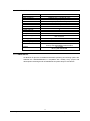
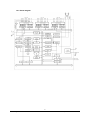
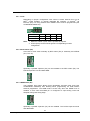
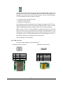
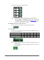
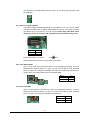
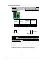
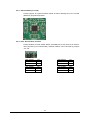
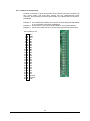
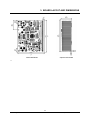
DBAT90USB162 Atmel® AT90USB162 Enhanced Development Board User’s manual 1 embeddedglow.com DBAT90USB162 Enhanced Development Board User’s Manual 1. INTRODUCTION ® Thank you for choosing the DBAT90USB162 – Atmel AT90USB162 enhanced development board. This board is designed to give both professionals and hobbyists a quick start to develop code and for hardware prototyping and testing. 1.1. OVERVIEW This document describes the DBAT90USB162 development board – a simple yet feature rich, flexible and easily configurable development tool, designed to allow easy coding and prototyping. ® The DBAT90USB162 is an enhanced Atmel AT90USB162 development board which also accepts AT90USB82. Offering modular design, this board is a costeffective yet feature rich, highly compatible, flexible and easily configurable development tool, designed to give a quick start to develop code and for hardware prototyping and testing. Its design provides configurability and flexibility not available with other products. The board provides all the basic circuitry needed to work with AT90USB162: USB connector and circuit, crystal and clock configuration circuitry, Reset and HWB buttons, status LED, user button and LED, power source/voltage configuration circuitry, configurable voltage regulator, isolation resistors to combine ISP lines with other functions. The board either accepts a MCU directly, or uses additional header boards for MCU installation giving the developer the freedom of using one development board with several MCUs, eventually programmed with different code. The board either accepts a MCU directly or uses additional header boards for MCU installation giving the developer the freedom of using one development board with several MCUs, eventually programmed with different code. An extension header is available allowing connection of various size universal boards such as the usually included UB100288 or breadboards holding the rest of the circuitry, and eventually using different hardware, or direct interfacing with other devices. Furthermore most board components are detachable or configurable via jumpers. The board offers flexible power: both 3.3 V and 5 V USB-powered or from external supply. The board also features a built-in voltage regulator, configurable to 3.3 V and 5 V with overcurrent and thermal protection. Board design makes it compatible with virtually all design/development software and libraries, including open source. 2 embeddedglow.com DBAT90USB162 Enhanced Development Board User’s Manual 1.2. FEATURES Flexible power – 3.3 V or 5 V from built-in voltage regulator, USB bus or external 3.0 V to 5.5 V; All MCU I/O pins are accessible; Headers for MCU header board – allows use of several MCUs (holding different firmware) with one development board; 100-mil extension header for connection to universal or breadboards, or direct interfacing with other devices, providing access to all I/O pins and virtually all signals; Dedicated headers for some signals: USB D-, D+, VBUS; RST/DW; HWB; EXTCLK, LED1, BUT1; Flexible I/O connections – virtually any 100 mil universal or breadboard can be attached using various connectors – allows using the board for more than one project; USB full speed (12 Mbps) Device mode supported; Type B and Mini USB connectors; Built-in 0.9..16 MHz crystal (default 8 MHz); Internal or external clock; Optional transient voltage suppression for USB data lines; Reset (RST) button; ® Hardware boot (HWB) button – allows forcing bootloader (stock Atmel or thirdparty) execution at reset (see AT90USB82/AT90USB162 datasheet) – allows MCU programming via USB without external programmer. I/O pin is still useable for other purposes; Detachable user button (BUT1) – general use button and/or used for debugging purposes. Can be disconnected to free I/O pin; Detachable user LED (LED1) – general use LED and/or used for debugging purposes. Can be disconnected to free I/O pin; FR-4 1.5 mm PCB with all terminals and components clearly marked, accepting TQFP-32, 7x7 mm body size, 0.8 mm lead pitch, and QFN-32, 5x5 mm body size, 0.5 mm lead pitch; ISP (6-pin) and JTAG (10-pin) connectors, both supporting in-circuit programming and debugging via debugWIRE; Switchable insulation resistors for all ISP pins (SCK, MOSI, MISO) and for HWB pin. 3 embeddedglow.com DBAT90USB162 Enhanced Development Board User’s Manual 1.3. SPECIFICATIONS Processor Flash memory Max. frequency RAM EEPROM USB USB DPRAM I/O lines Timers PWM channels USART SPI port Programming Debugging Operating voltage Operating temperature Dimensions Weight AT90USB162 16 kBytes (10,000 write cycles) 8 MHz at 2.7 V, 16 MHz at 4.5 V 512 Bytes (static) 512 Bytes (100,000 write cycles) USB 2.0 full speed (12 Mbps) Device mode 176 Bytes 22 1 8-bit, 1 16-bit 5 1 1 Via USB and hardware-initiated bootloader or ISP connector Via debugWIRE interface (ISP connector) 2.7 V to 5.5 V Industrial -40°C to +85°C 61 x 76 x 19 mm (2.4 x 3.0 in), 95 x 76 mm (3.7 x 3.0 x 0.75 in) with UB100288 universal board 31.4 g bare 39.25 g with UB100288 1.4. COMPATIBILITY As all MCU I/O pins are accessible and all MCU powering and clocking options are available the SBAT90USB162a is compatible with virtually every project and development tool designed for AT90USB162 and particularly for AVR MCUs. 4 embeddedglow.com DBAT90USB162 Enhanced Development Board User’s Manual 1.5. MCU OVERVIEW The AT90USB162 is a low-power CMOS 8-bit microcontroller based on the AVR enhanced RISC architecture. By executing powerful instructions in a single clock cycle, the AT90USB162 achieves throughputs approaching 1 MIPS per MHz allowing optimization of power consumption versus processing speed. 1.5.1. Features High Performance, Low Power AVR® 8-Bit Microcontroller Advanced RISC Architecture – 125 Powerful Instructions – Most Single Clock Cycle Execution – 32 x 8 General Purpose Working Registers – Fully Static Operation – Up to 16 MIPS Throughput at 16 MHz Non-volatile Program and Data Memories – 8K/16K Bytes of In-System Self-Programmable Flash • Endurance: 10,000 Write/Erase Cycles – Optional Boot Code Section with Independent Lock Bits • USB boot-loader programmed by default in the factory • In-System Programming by on-chip Boot Program hardwareactivated after reset • True Read-While-Write Operation – 512 Bytes EEPROM • Endurance: 100,000 Write/Erase Cycle – 512 Bytes Internal SRAM – Programming Lock for Software Security USB 2.0 Full-speed Device Module with Interrupt on Transfer Completion – Complies fully with Universal Serial Bus Specification REV 2.0 – 48 MHz PLL for Full-speed Bus Operation: data transfer rates at 12 Mbit/s – Fully independent 176 bytes USB DPRAM for endpoint memory allocation – Endpoint 0 for Control Transfers: from 8 up to 64-bytes – 4 Programmable Endpoints: • IN or Out Directions • Bulk, Interrupt and Isochronous Transfers • Programmable maximum packet size from 8 to 64 bytes • Programmable single or double buffer – Suspend/Resume Interrupts – Microcontroller reset on USB Bus Reset without detach – USB Bus Disconnection on Microcontroller Request – USB pad multiplexed with PS/2 peripheral for single cable capability Peripheral Features – PS/2 compliant pad – One 8-bit Timer/Counters with Separate Prescaler and Compare Mode (two 8-bit PWM channels) – One 16-bit Timer/Counter with Separate Prescaler, Compare and Capture Mode (three 8-bit PWM channels) – USART with SPI master only mode and hardware flow control (RTS/CTS) 5 embeddedglow.com DBAT90USB162 Enhanced Development Board User’s Manual – Master/Slave SPI Serial Interface – Programmable Watchdog Timer with Separate On-chip Oscillator – On-chip Analog Comparator – Interrupt and Wake-up on Pin Change On Chip Debug Interface (debugWIRE) Special Microcontroller Features – Power-On Reset and Programmable Brown-out Detection – Internal Calibrated Oscillator – External and Internal Interrupt Sources – Five Sleep Modes: Idle, Power-save, Power-down, Standby, and Extended Standby I/O and Packages – 22 Programmable I/O Lines – QFN32 (5x5 mm) / TQFP32 packages Operating Voltages – 2.7 - 5.5 V Operating temperature – Industrial (-40 °C to +85 °C) Maximum Frequency – 8 MHz at 2.7 V - Industrial range – 16 MHz at 4.5 V - Industrial range 6 embeddedglow.com DBAT90USB162 Enhanced Development Board User’s Manual 1.5.2. Block diagram 7 embeddedglow.com DBAT90USB162 Enhanced Development Board User’s Manual 1.5.3. Memory map 1.6. DEMO PROGRAM The DBAT90USB162 comes with a simple demo program installed. It makes LED1 blink, while pressing BUT1 changes the blinking rate. This program doesn’t provide USB compatibility. AVR-GCC source file is available for download at http://embeddedglow.com/products/DBAT90USB162/DBAT90USB162_Demo.c. HEX file is available for download at http://embeddedglow.com/products/DBAT90USB162/DBAT90USB162_Demo.hex. 2. USING THE DBAT90USB162 This section describes the board and all its features 8 embeddedglow.com DBAT90USB162 Enhanced Development Board User’s Manual 2.1. SCHEMATIC 9 embeddedglow.com DBAT90USB162 Enhanced Development Board User’s Manual 2.2. SCHEMATIC DESCRIPTION AND CONFIGURATION 2.2.1. Clock Depending on jumper configuration clock source is either internal from 0.9..16 (1) (2) MHz crystal oscillator, or internal calibrated RC oscillator, or external via EXTCLK (P2). For using external clock CKSEL fuses must be programmed (see AT90USB162 datasheet). Clock Internal crystal External J1 open short J2 short open J3 short open J4 open short Note: 1. Default is 8 MHz crystal, other is possible by request. 2. XTAL2 (PC0) can be used as generic I/O depending on MCU configuration. 2.2.2. Reset button (S2) Cold reset is done either manually by RST button (S2) or externally via RSTDW (P11, P21-27). Optionally a parallel capacitor (C5) can be installed to the RST button (S2). The PCB accepts thru-hole and 0805 SMD. 2.2.3. HWB button (S1) The hardware boot button allows forcing bootloader execution after reset (see AT90USB162 datasheet) thus allowing MCU programming via USB without external programmer. The HWB mode is active only when the HWBE fuse is enabled. In that case PD7/HWB pin is configured as input during reset and sampled during reset rising edge. Optionally a parallel capacitor (C4) can be installed. The PCB accepts thru-hole and 0805 SMD. 10 embeddedglow.com DBAT90USB162 Enhanced Development Board User’s Manual Programming via USB is based on pre-programmed USB bootloader, located in the on-chip boot section of the AT90USB162. This is the easiest and fastest way to reprogram the device directly over the USB interface, but with certain limitations. To force bootloader execution, operate as follows: Press both “RST” and “HWB” buttons; Release the “RST” button; Release the “HWB” button. ® FLIP (Flexible In-system Programmer) is the software provided by Atmel to do insystem programming of Flash devices through RS232, USB or CAN. For further details regarding programming via USB, please refer to FLIP documentation. Note: In order to use FLIP, driver installation is required. USB drivers come with ® FLIP and can be found in its install folder. If Windows operating system is used, depending on its version digitally signed drivers might be required. As they may not ® be supplied by Atmel , third-party signed drivers can be downloaded from the net. Tip: After programming is complete press the “RST” button. LUFA bootloader is also supported. 2.2.4. USB connector (1) Use either Type B USB (P3) or Mini-B USB (P1) . USB Type B connector pinout: Pin 1 2 3 4 Signal VCC DD+ GND USB Mini connector pinout: Pin 1 2 3 4 5 Description +5 V Data Data + Ground Signal VCC DD+ ID GND Description +5 V Data Data + NC for type B Ground 11 embeddedglow.com DBAT90USB162 Enhanced Development Board User’s Manual USB signals are available via headers as follows: Pin Signal 1 VCC 2 D- 3 D+ 4 GND Header Note: 1. Type B and Mini USB connectors cannot be used simultaneously. 2. New, unprogrammed AT90USB162 device is seen via USB as “AT90USB162 DFU”. To use USB driver installation is required. USB drivers can be downloaded from Atmel’s site: http://atmel.com/*. Thirdparty drivers are also available on the net. 2.2.5. USB data lines transient voltage suppression Data lines protection is available by using optional transils D2 and D3. 2.2.6. Power supply Both 3.3 V and 5 V VCC power can be used, supplied from USB, built-in regulator, or other source via VREG (P12). I/O voltage / VCC source 3 V I/O USB-powered 5 V I/O USB-powered (1) 3.0 to 3.6 V I/O self-powered (2) 3.4 to 5.5 V I/O self-powered J5 short open J6 open open short short J7 short open short open J8 open short open open J9 open open open short J10 short short open open Note: 1. 3.0 V to 3.6 V can be supplied via VREG (P12) instead of using the built in voltage regulator; 2. 3.4 V to 5.5 V can be supplied via VREG (P12) instead of using the built in voltage regulator. 12 embeddedglow.com DBAT90USB162 Enhanced Development Board User’s Manual VCC presence, no matter what the power source is, is indicated by the green VCC ON LED (D5). 2.2.7. Built-in voltage regulator The built-in voltage regulator depending on J5 produces 3.3 V or 5 V from a source, connected to PWR1 (P7) or PWR2 (P8). Based on LM1117, the voltage regulator can deliver up to 0.8 A from 5.2 V to 20 V input. Please obey maximum power dissipation, which is around 1.2 W, otherwise thermal shutdown may occur! VREG 3.3 V 5V J5 short open Power jack (PWR1, P7) pinout: Shottky diode D1 serves as a reverse polarity protection. 2.2.8. User button BUT1 BUT1 can be used as a general use button or for debugging purposes. It can be detached from PC2 by leaving J11 open. To use PC2 I/O pin for other purposes leave J11 open. BUT1 signal is available via header P13. Optionally capacitor C13 can be used. The PCB accepts thru-hole and 0805 SMD. BUT1 In use Not in use J11 short open 2.2.9.User LED LED1 LED1 can be used as a general use LED or for debugging purposes. It can be detached from PC4 by leaving J12 open. To use PC4 I/O pin for other purposes leave J11 open. LED1 signal is available via header P14. LED1 In use Not in use J12 short open 13 embeddedglow.com DBAT90USB162 Enhanced Development Board User’s Manual 2.2.10. ISP and JTAG connectors Both ISP (6-pin) (P15) and JTAG (10-pin) (P16) connectors offer identical functionality for in-circuit programming and debugging via debugWIRE (RST pin). If these connectors are in use, it is not recommended (although is possible) to use corresponding MCU pins as generic I/Os. ISP and JTAG connectors are pin-topin connected as follows: ISP (6-pin) JTAG (10-pin) Pin 3 SCK Pin 6 GND Pin 1 MISO Pin 2 VCC Pin 5 RST Pin 4 MOSI Pin 1 TCK Pin 2 GND Pin 3 TDO Pin 4 VTref Pin 6 nSRST Pin 9 TDI Debugging via debugWIRE X X X JTAG connector pinout: ISP connector pinout: 1 In-circuit programming X X X X X X 1 2 2 (SCK) TCK GND (MISO) TDO VTref (VCC) nSRST (RST) MISO VCC (VTG) SCK MOSI RST GND (MOSI) TDI The JTAG connector is intended for use with devices like JTAGICE mkII and AVR ONE!, but only offers in-circuit programming and debugging via debugWIRE as the full JTAG interface is not supported by AT90USB162. The JTAG 10-pin connector pinout is different from ISP 10-pin connector pinout, which is not implemented here! DO NOT CONNECT ISP 10-WIRE CABLES TO THE JTAG CONNECTOR! The debugWIRE interface uses only one pin, the RST pin, for communication with the target device. To enable the debugWIRE interface on an AVR device, the DWEN fuse must be programmed (DWEN = 0). AVR devices featuring debugWIRE are shipped with the DWEN fuse unprogrammed. ISP or High-Voltage Programming is required to enable debugWIRE. In order to use the ISP interface the SPIEN fuse must be programmed. 14 embeddedglow.com DBAT90USB162 Enhanced Development Board User’s Manual 2.2.11. MCU headers (P17..P20) Provide support for optional header boards for MCU allowing the use of several (differently programmed) MCUs. 2.2.12. R13..R16 isolation resistors Provide isolation for SCK, MISO, MOSI, and HWB pins, if they have to be used for other purposes (not recommended). Isolation resistors can be shorted by jumpers J13..J16. PB1 (SCLK) ISP Generic I/O J13 open short PB3 (MISO) ISP Generic I/O J15 open short PB2 (MOSI) ISP Generic I/O J14 open short PD7 (HWB) HWB Generic I/O J16 open short 15 embeddedglow.com DBAT90USB162 Enhanced Development Board User’s Manual 2.2.13. Extension header (P21) Provides connection to other devices and circuitry allowing access to all MCU I/O pins, power supply, and most other signals. Fits any 100mil/2.54mm linear connector, thus providing connectivity with virtually any 100mil/2.54mm universal or breadboard. Example 1: Use male/female headers and connect universal board like UB100288 or any third-party universal or breadboard. Example 2: Use a 100 mil / 2.54 mm terminal header to connect wires directly. Example 3: Use a 100 mil SIP socket to connect single parts like sensors directly. EXT header pinout: 1 2 3 4 5 6 7 8 9 10 11 12 13 14 15 16 17 18 19 20 21 22 23 24 25 26 27 28 VCC LED1 BUT1 PB0 PB1 PB2 PB3 PB4 PB5 PB6 PB7 PD0 PD1 PD2 PD3 PD4 PD5 PD6 PD7 PC0 PC2 PC4 PC5 PC6 PC7 EXTCLK RSTDW GND 16 embeddedglow.com DBAT90USB162 Enhanced Development Board User’s Manual 3. BOARD LAYOUT AND DIMENSIONS DBAT90USB162 Optional UB100288 □ 17 embeddedglow.com DBAT90USB162 Enhanced Development Board User’s Manual Disclaimer: All information in this document is provided in connection with embeddedglow.com products. No license, express or implied, by estoppel or otherwise, to any intellectual property right is granted by this document or in connection with the sale of embeddedglow.com products. EXCEPT AS SET FORTH IN EMBEDDEDGLOW.COM TERMS AND CONDITIONS OF SALE, WEBSITE OWNER ASSUMES NO LIABILITY WHATSOEVER AND DISCLAIMS ANY EXPRESS, IMPLIED OR STATUTORY WARRANTY RELATING TO HIS PRODUCTS INCLUDING, BUT NOT LIMITED TO, THE IMPLIED WARRANTY OF MERCHANTABILITY, FITNESS FOR A PARTICULAR PURPOSE, OR NONINFRINGEMENT. IN NO EVENT WILL WEBSITE OWNER BE LIABLE FOR ANY DIRECT, INDIRECT, CONSEQUENTIAL, PUNITIVE, SPECIAL OR INCIDENTAL DAMAGES, INCLUDING WITHOUT LIMITATION, DAMAGES FOR LOSS OF PROFITS, BUSINESS INTERRUPTION, OR LOSS OF INFORMATION, ARISING OUT OF THE USE OR INABILITY TO USE THIS DOCUMENT. Website owner makes no representations or warranties with respect to the accuracy or completeness of the contents of this document and reserves the right to make changes to specifications and product descriptions at any time without notice. Website owner does not make any commitment to update the information contained herein. Embeddedglow.com products are not intended, authorized, or suitable for, and shall not be used in automotive applications and/or as components in applications intended to support or sustain life. The content of this document is protected by Copyright. It cannot be copied or distributed in any way without the permission of the copyright holder. All rights are reserved. Atmel® logo and combinations thereof, and AVR® are registered trademarks or trademarks of Atmel Corporation or its subsidiaries. Windows® is a registered trademark of Microsoft Corporation. *As this document provides links to web pages and/or resources, the inclusion of those links is for reader's convenience only, and should not be interpreted as an endorsement of the owner/sponsor of the site or the content of the site. 18 embeddedglow.com DBAT90USB162 Enhanced Development Board User’s Manual