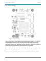
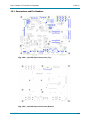
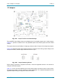
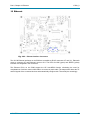
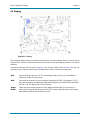
1
phyCORE-Vybrid
System on Module and Carrier Board
Hardware Manual
Document No: L-783e_0
Product No: PCM-052/PCM-952
SOM PCB No: 1374.0
CB PCB No: 1375.2
Edition: December 11, 2012
A product of a PHYTEC Technology Holding Company
L-783e_0
phyCORE-Vybrid
In this manual are descriptions for copyrighted products that are not explicitly indicated as such. The
absence of the trademark (™) and copyright (©) symbols does not imply that a product is not protected.
Additionally, registered patents and trademarks are similarly not expressly indicated in this manual.
The information in this document has been carefully checked and is believed to be entirely reliable.
However, PHYTEC America LLC assumes no responsibility for any inaccuracies. PHYTEC America LLC
neither gives any guarantee nor accepts any liability whatsoever for consequential damages resulting from
the use of this manual or its associated product. PHYTEC America LLC reserves the right to alter the
information contained herein without prior notification and accepts no responsibility for any damages which
might result.
Additionally, PHYTEC America LLC offers no guarantee nor accepts any liability for damages arising from
the improper usage or improper installation of the hardware or software. PHYTEC America LLC further
reserves the right to alter the layout and/or design of the hardware without prior notification and accepts no
liability for doing so.
© Copyright 2011 PHYTEC America LLC, Bainbridge Island, WA.
Rights - including those of translation, reprint, broadcast, photomechanical or similar reproduction and
storage or processing in computer systems, in whole or in part - are reserved. No reproduction may occur
without the express written consent from PHYTEC America LLC.
EUROPE
NORTH AMERICA
PHYTEC Technologie Holding AG
Robert-Koch-Str. 39
D-55129 Mainz
GERMANY
PHYTEC America LLC
203 Parfitt Way SW, Suite G100
Bainbridge Island, WA 98110
USA
+49 (800) 0749832
[email protected]
1 (800) 278-9913
[email protected]
Technical Support:
+49 (6131) 9221-31
[email protected]
1 (800) 278-9913
[email protected]
Fax:
+49 (6131) 9221-33
1 (206) 780-9135
http://www.phytec.eu
http://www.phytec.de
http://www.phytec.com
Address:
Ordering Information:
Website:
© PHYTEC America LLC 2012
L-783e_0
Table of Contents
L-783e_0
Table of Contents
List of Tables. . . . . . . . . . . . . . . . . . . . . . . . . . . . . . . . . . . . . . . . . . . . . . . . . . . . . . . . . .iii
List of Figures . . . . . . . . . . . . . . . . . . . . . . . . . . . . . . . . . . . . . . . . . . . . . . . . . . . . . . . . . iv
Conventions, Abbreviations, and Acronyms . . . . . . . . . . . . . . . . . . . . . . . . . . . . . . . . . . . . . . . . . . . . . v
Part I: PCM-052/phyCORE-Vybrid System on Module . . . . . . . . . . . . . . . . . . . . . . . . . . . . . . . . . . . . . 1
1 Introduction . . . . . . . . . . . . . . . . . . . . . . . . . . . . . . . . . . . . . . . . . . . . . . . . . . . . . . . . . . . . . . . . . . . . . . . 2
1.1 phyCORE-Vybrid Features . . . . . . . . . . . . . . . . . . . . . . . . . . . . . . . . . . . . . . . . . . . . . . . . . . . 2
1.2 Minimum Requirements to Operate the phyCORE-Vybrid . . . . . . . . . . . . . . . . . . . . . . . . . . . 3
1.3 Block Diagram . . . . . . . . . . . . . . . . . . . . . . . . . . . . . . . . . . . . . . . . . . . . . . . . . . . . . . . . . . . . . 4
1.4 View of the phyCORE-Vybrid . . . . . . . . . . . . . . . . . . . . . . . . . . . . . . . . . . . . . . . . . . . . . . . . . 5
2 Pin Description . . . . . . . . . . . . . . . . . . . . . . . . . . . . . . . . . . . . . . . . . . . . . . . . . . . . . . . . . . . . . . . . . . . . 7
3 Jumpers. . . . . . . . . . . . . . . . . . . . . . . . . . . . . . . . . . . . . . . . . . . . . . . . . . . . . . . . . . . . . . . . . . . . . . . . . 16
3.1 Jumper Settings. . . . . . . . . . . . . . . . . . . . . . . . . . . . . . . . . . . . . . . . . . . . . . . . . . . . . . . . . . . 17
4 Power . . . . . . . . . . . . . . . . . . . . . . . . . . . . . . . . . . . . . . . . . . . . . . . . . . . . . . . . . . . . . . . . . . . . . . . . . . 19
4.1 Primary System Power (VDD_3V3). . . . . . . . . . . . . . . . . . . . . . . . . . . . . . . . . . . . . . . . . . . . 19
4.2 DDR3 Power . . . . . . . . . . . . . . . . . . . . . . . . . . . . . . . . . . . . . . . . . . . . . . . . . . . . . . . . . . . . . 20
4.3 Vybrid Processor Core Power . . . . . . . . . . . . . . . . . . . . . . . . . . . . . . . . . . . . . . . . . . . . . . . . 20
4.4 Backup Power (VBAT). . . . . . . . . . . . . . . . . . . . . . . . . . . . . . . . . . . . . . . . . . . . . . . . . . . . . . 20
5 External RTC . . . . . . . . . . . . . . . . . . . . . . . . . . . . . . . . . . . . . . . . . . . . . . . . . . . . . . . . . . . . . . . . . . . . . 21
6 System Configuration and Booting . . . . . . . . . . . . . . . . . . . . . . . . . . . . . . . . . . . . . . . . . . . . . . . . . . . . 22
7 System Memory. . . . . . . . . . . . . . . . . . . . . . . . . . . . . . . . . . . . . . . . . . . . . . . . . . . . . . . . . . . . . . . . . . . 23
7.1 DDR3 SDRAM . . . . . . . . . . . . . . . . . . . . . . . . . . . . . . . . . . . . . . . . . . . . . . . . . . . . . . . . . . . . 23
7.2 NAND Flash. . . . . . . . . . . . . . . . . . . . . . . . . . . . . . . . . . . . . . . . . . . . . . . . . . . . . . . . . . . . . . 23
7.3 QSPI NOR Flash . . . . . . . . . . . . . . . . . . . . . . . . . . . . . . . . . . . . . . . . . . . . . . . . . . . . . . . . . . 23
7.4 I²C EEPROM . . . . . . . . . . . . . . . . . . . . . . . . . . . . . . . . . . . . . . . . . . . . . . . . . . . . . . . . . . . . . 23
7.4.1 Setting the EEPROM Lower Address Bits . . . . . . . . . . . . . . . . . . . . . . . . . . . . . . . 24
7.4.2 EEPROM Write Protection Control (J6). . . . . . . . . . . . . . . . . . . . . . . . . . . . . . . . . 24
7.5 Memory Model . . . . . . . . . . . . . . . . . . . . . . . . . . . . . . . . . . . . . . . . . . . . . . . . . . . . . . . . . . . . 24
8 Serial Interfaces. . . . . . . . . . . . . . . . . . . . . . . . . . . . . . . . . . . . . . . . . . . . . . . . . . . . . . . . . . . . . . . . . . . 25
8.1 SCI / RS-232 . . . . . . . . . . . . . . . . . . . . . . . . . . . . . . . . . . . . . . . . . . . . . . . . . . . . . . . . . . . . . 25
8.2 Ethernet . . . . . . . . . . . . . . . . . . . . . . . . . . . . . . . . . . . . . . . . . . . . . . . . . . . . . . . . . . . . . . . . . 25
8.3 FlexCAN . . . . . . . . . . . . . . . . . . . . . . . . . . . . . . . . . . . . . . . . . . . . . . . . . . . . . . . . . . . . . . . . 26
9 Technical Specifications . . . . . . . . . . . . . . . . . . . . . . . . . . . . . . . . . . . . . . . . . . . . . . . . . . . . . . . . . . . . 27
10 Integrating and Handling the phyCORE-Vybrid. . . . . . . . . . . . . . . . . . . . . . . . . . . . . . . . . . . . . . . . . . 29
10.1 Integrating the phyCORE-Vybrid . . . . . . . . . . . . . . . . . . . . . . . . . . . . . . . . . . . . . . . . . . . . . 29
10.2 Handling the phyCORE-Vybrid . . . . . . . . . . . . . . . . . . . . . . . . . . . . . . . . . . . . . . . . . . . . . . 30
Part II: PCM-952/phyCORE-Vybrid Carrier Board . . . . . . . . . . . . . . . . . . . . . . . . . . . . . . . . . . . . . . . .
11 Introduction . . . . . . . . . . . . . . . . . . . . . . . . . . . . . . . . . . . . . . . . . . . . . . . . . . . . . . . . . . . . . . . . . . . . .
12 Overview of Peripherals . . . . . . . . . . . . . . . . . . . . . . . . . . . . . . . . . . . . . . . . . . . . . . . . . . . . . . . . . . .
12.1 Connectors and Pin Headers . . . . . . . . . . . . . . . . . . . . . . . . . . . . . . . . . . . . . . . . . . . . . . .
12.2 Buttons and Switches . . . . . . . . . . . . . . . . . . . . . . . . . . . . . . . . . . . . . . . . . . . . . . . . . . . . .
12.2.1 System Reset Button . . . . . . . . . . . . . . . . . . . . . . . . . . . . . . . . . . . . . . . . . . . . . .
12.2.2 User Programmable Push Buttons . . . . . . . . . . . . . . . . . . . . . . . . . . . . . . . . . . .
12.2.3 Boot Configuration Switch . . . . . . . . . . . . . . . . . . . . . . . . . . . . . . . . . . . . . . . . . .
12.2.4 SPI Flash Button . . . . . . . . . . . . . . . . . . . . . . . . . . . . . . . . . . . . . . . . . . . . . . . . .
12.3 LEDs . . . . . . . . . . . . . . . . . . . . . . . . . . . . . . . . . . . . . . . . . . . . . . . . . . . . . . . . . . . . . . . . . .
12.3.1 User Programmable LEDs. . . . . . . . . . . . . . . . . . . . . . . . . . . . . . . . . . . . . . . . . .
13 Jumpers. . . . . . . . . . . . . . . . . . . . . . . . . . . . . . . . . . . . . . . . . . . . . . . . . . . . . . . . . . . . . . . . . . . . . . . .
© PHYTEC America LLC 2012
31
32
34
35
37
37
38
38
38
39
40
41
i
Table of Contents
L-783e_0
14 phyCORE-Vybrid SOM Connectivity . . . . . . . . . . . . . . . . . . . . . . . . . . . . . . . . . . . . . . . . . . . . . . . . . .
15 Power . . . . . . . . . . . . . . . . . . . . . . . . . . . . . . . . . . . . . . . . . . . . . . . . . . . . . . . . . . . . . . . . . . . . . . . . .
15.1 Wall Adapter Input . . . . . . . . . . . . . . . . . . . . . . . . . . . . . . . . . . . . . . . . . . . . . . . . . . . . . . . .
15.2 VBAT . . . . . . . . . . . . . . . . . . . . . . . . . . . . . . . . . . . . . . . . . . . . . . . . . . . . . . . . . . . . . . . . . .
15.3 Current Measurement . . . . . . . . . . . . . . . . . . . . . . . . . . . . . . . . . . . . . . . . . . . . . . . . . . . . .
16 Ethernet . . . . . . . . . . . . . . . . . . . . . . . . . . . . . . . . . . . . . . . . . . . . . . . . . . . . . . . . . . . . . . . . . . . . . . . .
17 RS-232 . . . . . . . . . . . . . . . . . . . . . . . . . . . . . . . . . . . . . . . . . . . . . . . . . . . . . . . . . . . . . . . . . . . . . . . .
18 CAN (Controller Area Network) . . . . . . . . . . . . . . . . . . . . . . . . . . . . . . . . . . . . . . . . . . . . . . . . . . . . . .
18.1 VCC_CAN . . . . . . . . . . . . . . . . . . . . . . . . . . . . . . . . . . . . . . . . . . . . . . . . . . . . . . . . . . . . . .
19 USB Connectivity. . . . . . . . . . . . . . . . . . . . . . . . . . . . . . . . . . . . . . . . . . . . . . . . . . . . . . . . . . . . . . . . .
19.1 VCC_USB . . . . . . . . . . . . . . . . . . . . . . . . . . . . . . . . . . . . . . . . . . . . . . . . . . . . . . . . . . . . . .
20 Display. . . . . . . . . . . . . . . . . . . . . . . . . . . . . . . . . . . . . . . . . . . . . . . . . . . . . . . . . . . . . . . . . . . . . . . . .
20.1 Display Signals . . . . . . . . . . . . . . . . . . . . . . . . . . . . . . . . . . . . . . . . . . . . . . . . . . . . . . . . . .
20.2 TFT Display . . . . . . . . . . . . . . . . . . . . . . . . . . . . . . . . . . . . . . . . . . . . . . . . . . . . . . . . . . . . .
20.3 PHYTEC Display Interface . . . . . . . . . . . . . . . . . . . . . . . . . . . . . . . . . . . . . . . . . . . . . . . . .
20.4 Touch Screen . . . . . . . . . . . . . . . . . . . . . . . . . . . . . . . . . . . . . . . . . . . . . . . . . . . . . . . . . . .
20.5 Light Sensor . . . . . . . . . . . . . . . . . . . . . . . . . . . . . . . . . . . . . . . . . . . . . . . . . . . . . . . . . . . .
21 SD/MMC . . . . . . . . . . . . . . . . . . . . . . . . . . . . . . . . . . . . . . . . . . . . . . . . . . . . . . . . . . . . . . . . . . . . . . .
22 Audio . . . . . . . . . . . . . . . . . . . . . . . . . . . . . . . . . . . . . . . . . . . . . . . . . . . . . . . . . . . . . . . . . . . . . . . . . .
23 JTAG . . . . . . . . . . . . . . . . . . . . . . . . . . . . . . . . . . . . . . . . . . . . . . . . . . . . . . . . . . . . . . . . . . . . . . . . . .
24 Trace . . . . . . . . . . . . . . . . . . . . . . . . . . . . . . . . . . . . . . . . . . . . . . . . . . . . . . . . . . . . . . . . . . . . . . . . . .
25 K20 . . . . . . . . . . . . . . . . . . . . . . . . . . . . . . . . . . . . . . . . . . . . . . . . . . . . . . . . . . . . . . . . . . . . . . . . . . .
26 Tamper . . . . . . . . . . . . . . . . . . . . . . . . . . . . . . . . . . . . . . . . . . . . . . . . . . . . . . . . . . . . . . . . . . . . . . . .
44
45
46
46
46
47
48
50
51
52
52
53
54
55
56
58
58
59
60
62
64
66
68
Part III: PCM-957/GPIO Expansion Board . . . . . . . . . . . . . . . . . . . . . . . . . . . . . . . . . . . . . . . . . . . . . . .
27 Introduction . . . . . . . . . . . . . . . . . . . . . . . . . . . . . . . . . . . . . . . . . . . . . . . . . . . . . . . . . . . . . . . . . . . . .
28 Analog Signal Mapping . . . . . . . . . . . . . . . . . . . . . . . . . . . . . . . . . . . . . . . . . . . . . . . . . . . . . . . . . . . .
29 Control Signal Mapping . . . . . . . . . . . . . . . . . . . . . . . . . . . . . . . . . . . . . . . . . . . . . . . . . . . . . . . . . . . .
30 Processor Signal Mapping. . . . . . . . . . . . . . . . . . . . . . . . . . . . . . . . . . . . . . . . . . . . . . . . . . . . . . . . . .
31 Power Signal Mapping. . . . . . . . . . . . . . . . . . . . . . . . . . . . . . . . . . . . . . . . . . . . . . . . . . . . . . . . . . . . .
69
70
71
72
73
75
Revision History . . . . . . . . . . . . . . . . . . . . . . . . . . . . . . . . . . . . . . . . . . . . . . . . . . . . . . . . . . . . . . . . . . . 76
© PHYTEC America LLC 2012
ii
List of Tables
L-783e_0
List of Tables
Conventions, Abbreviations, and Acronyms . . . . . . . . . . . . . . . . . . . . . . . . . . . . . . . . . . . . . . . . . . . . . v
Table 1-1. Abbreviations and Acronyms Used in This Manual . . . . . . . . . . . . . . . . . . . . . . . . . . . v
Table 1-2. Types of Signals . . . . . . . . . . . . . . . . . . . . . . . . . . . . . . . . . . . . . . . . . . . . . . . . . . . . . . vi
Part I: PCM-052/phyCORE-Vybrid System on Module . . . . . . . . . . . . . . . . . . . . . . . . . . . . . . . . . . . . . 1
Table 2-1. Pinout of the phyCORE-Connector X1, Row A . . . . . . . . . . . . . . . . . . . . . . . . . . . . . . 8
Table 2-2. Pinout of the phyCORE-Connector X1, Row B . . . . . . . . . . . . . . . . . . . . . . . . . . . . . 10
Table 2-3. Pinout of the phyCORE-Connector X1, Row C . . . . . . . . . . . . . . . . . . . . . . . . . . . . . 12
Table 2-4. Pinout of the phyCORE-Connector X1, Row D . . . . . . . . . . . . . . . . . . . . . . . . . . . . . 14
Table 3-1. SOM Jumper Settings . . . . . . . . . . . . . . . . . . . . . . . . . . . . . . . . . . . . . . . . . . . . . . . . 18
Table 6-1. Boot Device Selection . . . . . . . . . . . . . . . . . . . . . . . . . . . . . . . . . . . . . . . . . . . . . . . . 22
Table 7-1. U6 EEPROM I²C Address via J1 and J2 . . . . . . . . . . . . . . . . . . . . . . . . . . . . . . . . . . 24
Table 7-2. EEPROM Write-Protection States Via J6 . . . . . . . . . . . . . . . . . . . . . . . . . . . . . . . . . . 24
Table 8-1. SCI RS-232 Signal Locations . . . . . . . . . . . . . . . . . . . . . . . . . . . . . . . . . . . . . . . . . . . 25
Table 9-1. Technical Specifications . . . . . . . . . . . . . . . . . . . . . . . . . . . . . . . . . . . . . . . . . . . . . . . 28
Table 9-2. Part information for phyCORE Connectors (X1) . . . . . . . . . . . . . . . . . . . . . . . . . . . . 28
Part II: PCM-952/phyCORE-Vybrid Carrier Board . . . . . . . . . . . . . . . . . . . . . . . . . . . . . . . . . . . . . . . .
Table 12-1. phyCORE-Vybrid Connectors . . . . . . . . . . . . . . . . . . . . . . . . . . . . . . . . . . . . . . . . .
Table 12-2. Button Descriptions . . . . . . . . . . . . . . . . . . . . . . . . . . . . . . . . . . . . . . . . . . . . . . . . .
Table 12-3. Switch Settings (S5) . . . . . . . . . . . . . . . . . . . . . . . . . . . . . . . . . . . . . . . . . . . . . . . . .
Table 12-4. Boot Configuration Settings . . . . . . . . . . . . . . . . . . . . . . . . . . . . . . . . . . . . . . . . . . .
Table 12-5. LED Descriptions . . . . . . . . . . . . . . . . . . . . . . . . . . . . . . . . . . . . . . . . . . . . . . . . . . .
Table 13-1. Jumper Settings and Descriptions . . . . . . . . . . . . . . . . . . . . . . . . . . . . . . . . . . . . . .
Table 15-1. Voltage Domains . . . . . . . . . . . . . . . . . . . . . . . . . . . . . . . . . . . . . . . . . . . . . . . . . . .
Table 15-2. Power LEDs . . . . . . . . . . . . . . . . . . . . . . . . . . . . . . . . . . . . . . . . . . . . . . . . . . . . . . .
Table 17-1. X10 Pin Descriptions . . . . . . . . . . . . . . . . . . . . . . . . . . . . . . . . . . . . . . . . . . . . . . . .
Table 17-2. X31 Pin Descriptions . . . . . . . . . . . . . . . . . . . . . . . . . . . . . . . . . . . . . . . . . . . . . . . .
Table 18-1. CAN0 Jumper Settings . . . . . . . . . . . . . . . . . . . . . . . . . . . . . . . . . . . . . . . . . . . . . . .
Table 18-2. VCC_CAN Supply Configuration . . . . . . . . . . . . . . . . . . . . . . . . . . . . . . . . . . . . . . .
Table 20-1. TTL Display Pin Header (X24) . . . . . . . . . . . . . . . . . . . . . . . . . . . . . . . . . . . . . . . . .
Table 20-2. TTL Display Connector (X29) . . . . . . . . . . . . . . . . . . . . . . . . . . . . . . . . . . . . . . . . . .
Table 20-3. PDI Connector (X30A) Signal Descriptions . . . . . . . . . . . . . . . . . . . . . . . . . . . . . . .
Table 20-4. PDI Connector (X30B) Signal Descriptions . . . . . . . . . . . . . . . . . . . . . . . . . . . . . . .
Table 22-1. Audio Connectors . . . . . . . . . . . . . . . . . . . . . . . . . . . . . . . . . . . . . . . . . . . . . . . . . . .
Table 23-1. JTAG Connector X16 Signals . . . . . . . . . . . . . . . . . . . . . . . . . . . . . . . . . . . . . . . . .
Table 23-2. JTAG Connector X19 Signals . . . . . . . . . . . . . . . . . . . . . . . . . . . . . . . . . . . . . . . . .
Table 24-1. Trace Connector X22 Pins . . . . . . . . . . . . . . . . . . . . . . . . . . . . . . . . . . . . . . . . . . . .
Table 25-1. K20 Jumper Configurations . . . . . . . . . . . . . . . . . . . . . . . . . . . . . . . . . . . . . . . . . . .
Table 26-1. Tamper Signals at Connector X21 . . . . . . . . . . . . . . . . . . . . . . . . . . . . . . . . . . . . . .
31
36
37
38
38
39
42
45
45
49
49
51
51
54
55
56
57
61
62
63
64
67
68
Part III: PCM-957/GPIO Expansion Board . . . . . . . . . . . . . . . . . . . . . . . . . . . . . . . . . . . . . . . . . . . . . . .
Table 28-1. Analog Signal Map . . . . . . . . . . . . . . . . . . . . . . . . . . . . . . . . . . . . . . . . . . . . . . . . . .
Table 29-1. Control Signal Map . . . . . . . . . . . . . . . . . . . . . . . . . . . . . . . . . . . . . . . . . . . . . . . . . .
Table 30-1. Processor Signal Map . . . . . . . . . . . . . . . . . . . . . . . . . . . . . . . . . . . . . . . . . . . . . . .
Table 31-1. Power Signal Map . . . . . . . . . . . . . . . . . . . . . . . . . . . . . . . . . . . . . . . . . . . . . . . . . .
69
71
72
73
75
Revision History . . . . . . . . . . . . . . . . . . . . . . . . . . . . . . . . . . . . . . . . . . . . . . . . . . . . . . . . . . . . . . . . . . . 76
Table 32-1. Revision History . . . . . . . . . . . . . . . . . . . . . . . . . . . . . . . . . . . . . . . . . . . . . . . . . . . . 76
© PHYTEC America LLC 2012
iii
List of Figures
L-783e_0
List of Figures
Part I: PCM-052/phyCORE-Vybrid System on Module . . . . . . . . . . . . . . . . . . . . . . . . . . . . . . . . . . . . . . 1
Fig. 1-1. phyCORE-Vybrid Block Diagram . . . . . . . . . . . . . . . . . . . . . . . . . . . . . . . . . . . . . . . . . . . 4
Fig. 1-2. Top View of the phyCORE-Vybrid (Controller Side). . . . . . . . . . . . . . . . . . . . . . . . . . . . . 5
Fig. 1-3. Bottom View of the phyCORE-Vybrid (Connector Side) . . . . . . . . . . . . . . . . . . . . . . . . . 6
Fig. 2-1. Pin-out of the phyCORE-Connector (Top View, with Cross Section Insert) . . . . . . . . . . . 8
Fig. 3-1. Jumper Numbering. . . . . . . . . . . . . . . . . . . . . . . . . . . . . . . . . . . . . . . . . . . . . . . . . . . . . 16
Fig. 3-2. Jumper Locations . . . . . . . . . . . . . . . . . . . . . . . . . . . . . . . . . . . . . . . . . . . . . . . . . . . . . . 17
Fig. 4-1. phyCORE-Vybrid Power Design . . . . . . . . . . . . . . . . . . . . . . . . . . . . . . . . . . . . . . . . . . 19
Fig. 9-1. phyCORE-Vybrid Physical Dimensions . . . . . . . . . . . . . . . . . . . . . . . . . . . . . . . . . . . . . 27
Fig. 10-1. phyCORE-Vybrid Footprint. . . . . . . . . . . . . . . . . . . . . . . . . . . . . . . . . . . . . . . . . . . . . . 29
Part II: PCM-952/phyCORE-Vybrid Carrier Board . . . . . . . . . . . . . . . . . . . . . . . . . . . . . . . . . . . . . . . . .
Fig. 11-1. phyCORE-Vybrid Carrier Board . . . . . . . . . . . . . . . . . . . . . . . . . . . . . . . . . . . . . . . . . .
Fig. 12-1. Overview of Peripherals . . . . . . . . . . . . . . . . . . . . . . . . . . . . . . . . . . . . . . . . . . . . . . . .
Fig. 12-2. phyCORE-Vybrid Connectors (Top) . . . . . . . . . . . . . . . . . . . . . . . . . . . . . . . . . . . . . . .
Fig. 12-3. phyCORE-Vybrid Connectors (Bottom) . . . . . . . . . . . . . . . . . . . . . . . . . . . . . . . . . . . .
Fig. 12-4. Buttons and Switches . . . . . . . . . . . . . . . . . . . . . . . . . . . . . . . . . . . . . . . . . . . . . . . . . .
Fig. 12-5. LEDs. . . . . . . . . . . . . . . . . . . . . . . . . . . . . . . . . . . . . . . . . . . . . . . . . . . . . . . . . . . . . . .
Fig. 13-1. Jumper Locations and Default Settings . . . . . . . . . . . . . . . . . . . . . . . . . . . . . . . . . . . .
Fig. 13-2. Jumper Numbering Scheme . . . . . . . . . . . . . . . . . . . . . . . . . . . . . . . . . . . . . . . . . . . .
Fig. 14-1. phyCORE-Vybrid SOM Connectivity to the Carrier Board . . . . . . . . . . . . . . . . . . . . . .
Fig. 15-1. Powering Scheme . . . . . . . . . . . . . . . . . . . . . . . . . . . . . . . . . . . . . . . . . . . . . . . . . . . .
Fig. 16-1. Ethernet Interface Connectors . . . . . . . . . . . . . . . . . . . . . . . . . . . . . . . . . . . . . . . . . . .
Fig. 17-1. RS-232 Interface Connectors . . . . . . . . . . . . . . . . . . . . . . . . . . . . . . . . . . . . . . . . . . . .
Fig. 17-2. DB-9 RS-232 Connectors P1A and P1B Pin Numbering . . . . . . . . . . . . . . . . . . . . . . .
Fig. 18-1. CAN Interface Connectors and Jumpers . . . . . . . . . . . . . . . . . . . . . . . . . . . . . . . . . . .
Fig. 19-1. USB Interface . . . . . . . . . . . . . . . . . . . . . . . . . . . . . . . . . . . . . . . . . . . . . . . . . . . . . . . .
Fig. 20-1. Display . . . . . . . . . . . . . . . . . . . . . . . . . . . . . . . . . . . . . . . . . . . . . . . . . . . . . . . . . . . . .
Fig. 21-1. SD/MMC Interface . . . . . . . . . . . . . . . . . . . . . . . . . . . . . . . . . . . . . . . . . . . . . . . . . . . .
Fig. 22-1. Audio Interface . . . . . . . . . . . . . . . . . . . . . . . . . . . . . . . . . . . . . . . . . . . . . . . . . . . . . . .
Fig. 23-1. JTAG Connectivity . . . . . . . . . . . . . . . . . . . . . . . . . . . . . . . . . . . . . . . . . . . . . . . . . . . .
Fig. 24-1. Trace . . . . . . . . . . . . . . . . . . . . . . . . . . . . . . . . . . . . . . . . . . . . . . . . . . . . . . . . . . . . . .
Fig. 25-1. K20 . . . . . . . . . . . . . . . . . . . . . . . . . . . . . . . . . . . . . . . . . . . . . . . . . . . . . . . . . . . . . . . .
Fig. 26-1. Tamper . . . . . . . . . . . . . . . . . . . . . . . . . . . . . . . . . . . . . . . . . . . . . . . . . . . . . . . . . . . . .
31
32
34
35
35
37
39
41
41
44
45
47
48
48
50
52
53
59
60
62
64
66
68
Part III: PCM-957/GPIO Expansion Board . . . . . . . . . . . . . . . . . . . . . . . . . . . . . . . . . . . . . . . . . . . . . . . 69
Fig. 27-1. PCM-957/GPIO Expansion Board and Patch Field . . . . . . . . . . . . . . . . . . . . . . . . . . . 70
© PHYTEC America LLC 2012
iv
L-783e_0
Conventions, Abbreviations, and Acronyms
Conventions
The conventions used in this manual are as follows:
• Signals that are preceded by a “/” character are designated as active low signals. Their active
state is when they are driven low, or are driving low; for example: /RESET.
• Tables show the default setting or jumper position in bold, teal text.
• Text in blue indicates a hyperlink, either internal or external to the document. Click these links to
quickly jump to the applicable URL, part, chapter, table, or figure.
• References made to the phyCORE-Connector always refer to the high density Samtec connectors
on the underside of the phyCORE-Vybrid System on Module.
Abbreviations and Acronyms
Many acronyms and abbreviations are used throughout this manual. Use the table below to navigate
unfamiliar terms used in this document.
Table 1-1. Abbreviations and Acronyms Used in This Manual
Abbreviation
Definition
BSP
Board Support Package (Software delivered with the Development Kit including an
operating system (Windows or Linux) preinstalled on the module and Development
Tools).
CB
Carrier Board; used in reference to the PCM-952/phyCORE-Vybrid Carrier Board
DFF
D flip-flop
EMB
External memory bus
EMI
Electromagnetic Interference
GPI
General purpose input
GPIO
General purpose input and output
GPO
General purpose output
IRAM
Internal RAM; the internal static RAM on the Freescale VFx00 processor
J
Solder jumper; these types of jumpers require solder equipment to remove and
place
JP
Solderless jumper; these types of jumpers can be removed and placed by hand with
no special tools
PCB
Printed circuit board
PDI
PHYTEC Display Interface; defined to connect PHYTEC display adapter boards or
custom adapters
PEB
PHYTEC Extension Board
PMIC
Power Management Integrated Circuit
PoE
Power over Ethernet
PoP
Package on Package
PoR
Power-on reset
RTC
Real-time clock
SMT
Surface mount technology
SOM
System on Module; used in reference to the PCM-052/phyCORE-Vybrid System on
Module
© PHYTEC America LLC 2012
v
L-783e_0
Table 1-1. Abbreviations and Acronyms Used in This Manual
Abbreviation
Definition
Sx
User button Sx (S1, S2, etc.) used in reference to the available user buttons, or DIP
switches on the Carrier Board
Sx_y
Switch y of DIP switch Sx; used in reference to the DIP switch on the Carrier Board
TRM
Technical Reference Manual
VBAT
SOM battery supply input
Different types of signals are brought out at the phyCORE-Connector. The following table lists the
abbreviations used to specify the type of a signal.
Table 1-2. Types of Signals
Type of Signal
Description
Abbreviation
Power
Supply voltage
PWR
Ref-Voltage
Reference voltage
REF
USB-Power
USB voltage
USB
Input
Digital input
IN
Output
Digital output
OUT
Input with pull-up
Input with pull-up (jumper or open-collector output)
IPU
Input/output
Bidirectional input/output
IO
5V Input with pull-down
5V tolerant input with pull-down
5V_PD
LVDS
Differential line pairs 100 Ohm LVDS Pegel
LVDS
Differential 90 Ohm
Differential line pairs 90 Ohm
DIFF90
Differential 100 Ohm
Differential line pairs 100 Ohm
DIFF100
Analog
Analog input or output
Analog
© PHYTEC America LLC 2012
vi
L-783e_0
Preface
This phyCORE-Vybrid Hardware Manual describes the System on Module's design and functions. Precise
specifications for the Freescale VFx00 processor can be found in the processor datasheet and/or user's
manual.
In this hardware manual and in the schematics, active low signals are denoted by a "/" preceding the signal
name, for example: /RD. A "0" represents a logic-zero or low-level signal, while a "1" represents a logicone or high-level signal.
Declaration of Electro Magnetic Conformity of the PHYTEC
phyCORE-Vybrid
PHYTEC System on Modules (SOMs) are designed for installation in electrical appliances or, combined
with the PHYTEC Carrier Board, can be used as dedicated Evaluation Boards (for use as a test and
prototype platform for hardware/software development) in laboratory environments.
CAUTION:
PHYTEC products lacking protective enclosures are subject to damage by ESD and, hence, may only be
unpacked, handled or operated in environments in which sufficient precautionary measures have been
taken in respect to ESD-dangers. It is also necessary that only appropriately trained personnel (such as
electricians, technicians and engineers) handle and/or operate these products. Moreover, PHYTEC
products should not be operated without protection circuitry if connections to the product's pin header
rows are longer than 3 m.
PHYTEC products fulfill the norms of the European Union's Directive for Electro Magnetic Conformity only
in accordance to the descriptions and rules of usage indicated in this hardware manual (particularly in
respect to the pin header row connectors, power connector and serial interface to a host-PC).
Implementation of PHYTEC products into target devices, as well as user modifications and extensions of
PHYTEC products, is subject to renewed establishment of conformity to, and certification of, Electro
Magnetic Directives. Users should ensure conformance following any modifications to the products as
well as implementation of the products into target systems.
The phyCORE-Vybrid is one of a series of PHYTEC System on Modules that can be populated with
different controllers and, hence, offers various functions and configurations. PHYTEC supports a variety of
8-/16- and 32-bit controllers in two ways:
1. As the basis for Rapid Development Kits which serve as a reference and evaluation platform.
2. As insert-ready, fully functional phyCORE OEM modules, which can be embedded directly into the
user's peripheral hardware design.
Implementation of an OEM-able SOM subassembly as the "core" of your embedded design allows you to
focus on hardware peripherals and firmware without expending resources to "re-invent" microcontroller
circuitry. Furthermore, much of the value of the phyCORE module lies in its layout and test.
Production-ready Board Support Packages (BSPs) and Design Services for our hardware further reduce
development time and expenses. Take advantage of PHYTEC products to shorten time-to-market, reduce
development costs, and avoid substantial design issues and risks. For more information go to:
http://www.phytec.com/services/design-services/index.html
© PHYTEC America LLC 2012
vii
L-783e_0
Product Change Management
In addition to our HW and SW offerings, the buyer will receive a free obsolescence maintenance service
for the HW provided when purchasing a PHYTEC SOM.
Our Product Change Management Team of developers is continuously processing all incoming PCN's
(Product Change Notifications) from vendors and distributors concerning parts which are being used in our
products. Possible impacts to the functionality of our products, due to changes of functionality or obsolesce
of a certain part, are evaluated in order to take the right measures in purchasing or within our HW/SW
design.
Our general philosophy here is: We never discontinue a product as long as there is demand for it.
Therefore a set of methods has been established to fulfill our philosophy:
Avoidance strategies
• Avoid changes by evaluating longevity of a parts during design-in phase.
• Ensure availability of equivalent second source parts.
• Maintain close contact with part vendors for awareness of roadmap strategies.
Change management in case of functional changes
• Avoid impacts on Product functionality by choosing equivalent replacement parts.
• Avoid impacts on Product functionality by compensating changes through HW redesign or
backward compatibility
SW maintenance
• Provide early change notifications concerning functional relevant changes of our Products.
Change management in rare event of an obsolete and non replaceable part
• Ensure long term availability by stocking parts through last time buy management, according to
product forecasts.
• Offer long term frame contract to customers.
We refrain from providing detailed, part-specific information within this manual, which is subject to
changes, due to ongoing part maintenance for our products.
© PHYTEC America LLC 2012
viii
PCM-052/phyCORE-Vybrid System on Module
L-783e_0
Part I: PCM-052/phyCORE-Vybrid System on
Module
Part 1 of this three part manual provides detailed information on the phyCORE-Vybrid System on Module
(SOM) designed for custom integration into customer applications.
The information in the following chapters is applicable to the 1374.0 PCB revision of the phyCORE-Vybrid
SOM.
© PHYTEC America LLC 2012
1
Part I, Chapter 1: Introduction
L-783e_0
1 Introduction
The phyCORE-Vybrid belongs to PHYTEC’s phyCORE System on Module (SOM) family. The
phyCORE SOMs represent the continuous development of PHYTEC SOM technology. Like its mini-,
micro-, and nanoMODUL predecessors, the phyCORE boards integrate all core elements of a
microcontroller system on a subminiature board and are designed in a manner that ensures their easy
expansion and embedding in peripheral hardware developments.
As independent research indicates that approximately 70% of all EMI (Electro Magnetic Interference)
problems stem from insufficient supply voltage grounding of electronic components in high frequency
environments, the phyCORE board design features an increased pin package. The increased pin package
allows dedication of approximately 20% of all connector pins on the phyCORE boards to ground. This
improves EMI and EMC characteristics and makes it easier to design complex applications meeting EMI
and EMC guidelines using phyCORE boards even in high noise environments.
phyCORE boards achieve their small size through modern SMD technology and multi-layer design. In
accordance with the complexity of the module, 0402-packaged SMD components and laser-drilled
Microvias are used on the boards, providing phyCORE users with access to this cutting edge
miniaturization technology for integration into their own design.
The phyCORE-Vybrid is a sub-miniature (41 x 51 mm) insert-ready SOM populated with Freescale FVx00
processor. Its universal design enables its insertion into a wide range of embedded applications. All
processor signals and ports extend from the processor to high-density pitch (0.5 mm) connectors aligning
two sides of the board. This allows the SOM to be plugged like a "big chip" into a target application.
Precise specifications for the processor populating the board can be found in the applicable processor
user's manual and datasheet. The descriptions in this manual are based on the Freescale FVx00
processor. No description of compatible processor derivative functions is included, as such functions are
not relevant for the basic functioning of the phyCORE-Vybrid.
1.1 phyCORE-Vybrid Features
•
•
•
•
•
•
•
•
•
•
•
•
•
•
Insert-ready, sub-miniature (41 mm x 51 mm) System on Module (SOM) subassembly in low EMI
design, achieved through advanced SMD technology
Populated with the Freescale FVx00 Single (Cortex-A5) or heterogenous Dual Core (Cortex-A5
and Cortex-M4) processor
Max. 500 MHz core clock frequency for the Cortex-A5, 167 MHz for the Cortex-M4
Boot from NAND Flash or SPI Flash
Controller signals and ports extend to two high-density (0.5 mm) Samtec connectors aligning two
sides of the board, enabling it to be plugged like a "big chip" into target application
Single supply voltage of 3.3 V (max.1 A)
All controller required supplies generated on board
Improved interference safety achieved through multi-layer PCB technology and dedicated ground
pins
256 MB (up to 2 GB) on-board NAND Flash1
128/256/512 MB DDR3 SDRAM 1
4 kB (up to 32 kB) I2C EEPROM1
32 MB (up to 128 MB) SPI Flash
Two RS-232 two-signal (Tx/Rx) serial interfaces, or one RS-232 interface with hardware flow
control, configured through software
Dual USB OTG 2.0 High-Speed Controller with PHY
1. The maximum memory size listed is as of the printing of this manual. Please contact PHYTEC for more information
about additional, or new module configurations available.
© PHYTEC America LLC 2012
2
Part I, Chapter 1: Introduction
•
•
•
•
•
•
•
•
•
•
•
•
•
•
•
L-783e_0
Two 10/100 MBit Ethernet interfaces with internal L2-Switch and IEEE1588 PTP for Realtime
Ethernet (available as RMII TTL signals or 10/100 differential pairs)
One I2C interface with SMBUS support
Four Serial Peripheral Interfaces (SPI)
Two Quad SPI (QSPI) supporting XIP
Two FlexCAN interfaces with transceivers
Display interface with 24 data bits
I2S audio
Two 12-bit digital to analog converter (DAC) outputs
Two 10-channel, 12-bit analog to digital (ADC) inputs
JTAG
16-bit Trace port
Two active and two passive tamper security signals
4-bit Secure Digital Host interface (SD/MMC)
Real-Time Clock
-40 to 85 C operating temperature range
1.2 Minimum Requirements to Operate the phyCORE-Vybrid
Basic operation of the phyCORE-Vybrid requires a 3.3V +-5% supply voltage with at least 1.0A current
capacity. Connect power and ground to the following pins on connector X1 to power the SOM:
3.3V: X1-1C, 2C, 1D, 2D
GND: X1-3C, 3D, 7C, 7D
Please refer to Chapter 2 for information on additional GND pins located at the phyCORE-Connector X1.
CAUTION:
We recommend connecting all available 3.3V input pins to the power supply system on a custom carrier
board housing the phyCORE-Vybrid and at least the matching number of GND pins neighboring the 3.3V
pins. In addition, proper implementation of the phyCORE-Vybrid module into a target application also
requires connecting all GND pins neighboring signals that are being used in the application circuitry.
Please refer to Chapter 4 for more information.
© PHYTEC America LLC 2012
3
Part I, Chapter 1: Introduction
L-783e_0
1.3 Block Diagram
Fig. 1-1. phyCORE-Vybrid Block Diagram
© PHYTEC America LLC 2012
4
Part I, Chapter 1: Introduction
L-783e_0
1.4 View of the phyCORE-Vybrid
Fig. 1-2. Top View of the phyCORE-Vybrid (Controller Side)
© PHYTEC America LLC 2012
5
Part I, Chapter 1: Introduction
L-783e_0
Fig. 1-3. Bottom View of the phyCORE-Vybrid (Connector Side)
© PHYTEC America LLC 2012
6
Part I, Chapter 2: Pin Description
L-783e_0
2 Pin Description
Please note that all module connections are not to exceed their expressed maximum voltage or current.
Maximum signal input values are indicated in the corresponding controller manuals/datasheets. As
damage from improper connections varies according to use and application, it is the user's responsibility to
take appropriate safety measures to ensure that the module connections are protected from overloading
through connected peripherals.
All controller signals extend to surface mount technology (SMT) connectors (0.5 mm) lining two sides of
the module (referred to as the phyCORE-Connector). This allows the phyCORE-Vybrid to be plugged into
any target application like a "big chip."
The numbering scheme for the phyCORE-Connector is based on a two dimensional matrix in which
column positions are identified by a letter and row position by a number. Pin 1A, for example, is always
located in the upper left hand corner of the matrix. The pin numbering values increase moving down on the
board. Lettering of the pin connector rows progresses alphabetically from left to right (refer to Figure 2-1).
The numbered matrix can be aligned with the phyCORE-Vybrid (viewed from above; phyCORE-Connector
pointing down) or with the socket of the corresponding phyCORE Carrier Board/user target circuitry. The
upper left-hand corner of the numbered matrix (pin 1A) is thus covered with the corner of the phyCOREVybrid marked with a number 1. The numbering scheme is always in relation to the PCB as viewed from
above, even if all connector contacts extend to the bottom of the module.
The numbering scheme is thus consistent for both the module’s phyCORE-Connector as well as mating
connectors on the phyCORE Carrier Board or target hardware, thereby considerably reducing the risk of
pin identification errors.
Since the pins are exactly defined according to the numbered matrix previously described, the phyCOREConnector is usually assigned a single designator for its position (X2 for example). In this manner the
phyCORE-Connector comprises a single, logical unit regardless of the fact that it could consist of more
than one physical socketed connector. The location of row 1 on the board is marked by a number 1 on the
PCB to allow easy identification.
Figure 2-1 illustrates the numbered matrix system. It shows a phyCORE-Vybrid with SMT phyCOREConnectors on its underside (defined as dotted lines) mounted on a Carrier Board. In order to facilitate
understanding of the pin assignment scheme, the diagram presents a cross-view of the phyCORE module
showing these phyCORE-Connectors mounted on the underside of the module’s PCB.
© PHYTEC America LLC 2012
7
Part I, Chapter 2: Pin Description
L-783e_0
Fig. 2-1. Pin-out of the phyCORE-Connector
(Top View, with Cross Section Insert)
The following tables provide an overview of the pinouts of the phyCORE-Connector with signal names and
descriptions specific to the phyCORE-Vybrid. It also provides the appropriate signal level interface
voltages listed in the SL (Signal Level) column and the signal direction.
CAUTION:
Most of the controller pins have multiple functions. Because most of these pins are connected directly to
the phyCORE-Connector the functions are also available there. Signal names and descriptions below
are in regard to the specification of the phyCORE-Vybrid and the functions defined therein. Please refer
to the VFx00 datasheet or TRM for more information about alternative functions. In order to utilize a specific pin's alternative function the corresponding registers must be configured within the appropriate
driver of the BSP. To support all features of the phyCORE-Vybrid Carrier Board a few changes have been
made in the BSP delivered with the module.
Table 2-1. Pinout of the phyCORE-Connector X1, Row A
Pin#
Signal
Type
SL
Description
1A
MCU_PTB0
IO
VDD_3V3
Display brightness control
2A
GND
-
-
Ground 0 V
3A
MCU_PTB4
IO
VDD_3V3
SCI1_TX serial transmit signal
4A
MCU_PTB5
IO
VDD_3V3
SCI1_RX serial receive signal
5A
MCU_PTB6
IO
VDD_3V3
SCI22_TX serial transmit signal, or SCI1_RTS
request to send
6A
MCU_PTB7
IO
VDD_3V3
SCI2_RX serial receive signal, or SCI1_CTS clear
to send
7A
GND
-
-
Ground 0 V
8A
MCU_PTB12
IO
VDD_3V3
Display Up/Down control
9A
MCU_PTB13
IO
VDD_3V3
Trace control
© PHYTEC America LLC 2012
8
Part I, Chapter 2: Pin Description
L-783e_0
Table 2-1. Pinout of the phyCORE-Connector X1, Row A (Continued)
Pin#
Signal
Type
SL
Description
10A
CAN_EN
IPU
VDD_3V3
Drive low to disable the CAN transceivers on the
SOM.
11A
RTC_INTn
OUT
VDD_3V3
External Real Time Clock interrupt/alarm
12A
GND
-
-
Ground 0 V
13A
MCU_PTB21
IO
VDD_3V3
SPI0 Master-In-Slave-Out (MISO)
14A
MCU_PTB22
IO
VDD_3V3
SPI0 clock
15A
MCU_PTB23
IO
VDD_3V3
GPIO
16A
MCU_PTB24
IO
VDD_3V3
NAND Flash write enable
17A
GND
-
-
Ground 0 V
18A
MCU_PTD16
IO
VDD_3V3
NAND Flash IO0
19A
MCU_PTD17
IO
VDD_3V3
NAND Flash IO1
20A
MCU_PTD18
IO
VDD_3V3
NAND Flash IO2
21A
MCU_PTD19
IO
VDD_3V3
NAND Flash IO3
22A
GND
-
-
Ground 0 V
23A
MCU_PTD24
IO
VDD_3V3
NAND Flash IO8
24A
MCU_PTD25
IO
VDD_3V3
NAND Flash IO9
25A
MCU_PTD26
IO
VDD_3V3
NAND Flash IO10
26A
MCU_PTD27
IO
VDD_3V3
NAND Flash IO11
27A
GND
-
-
Ground 0 V
28A
MCU_PTC26
IO
VDD_3V3
NAND Flash Ready / Busy
29A
MCU_PTC27
IO
VDD_3V3
NAND Flash address latch enable
30A
MCU_PTC28
IO
VDD_3V3
NAND Flash command latch enable
31A
MCU_PTC29
-
VDD_3V3
GPIO
32A
GND
-
-
Ground 0 V
33A
MCU_PTC30
IO
VDD_3V3
GPIO
34A
MCU_PTD0
OUT
VDD_3V3
QSPI0_A clock
35A
MCU_PTD1
IO
VDD_3V3
QSPI0_A chip select
36A
MCU_PTD2
IO
VDD_3V3
QSPI0_A hold
37A
GND
-
-
Ground 0 V
38A
MCU_PTD3
IO
VDD_3V3
QSPI0_A write-protect
39A
MCU_PTD4
IO
VDD_3V3
QSPI0_A data 1
40A
MCU_PTD5
IO
VDD_3V3
QSPI0_A data 0
41A
MCU_PTD6
IO
VDD_3V3
SD Card Detect (SDCD)
42A
GND
-
-
Ground 0 V
43A
MCU_PTC4
IO
VDD_3V3
RMII0 Receive Data 0
44A
MCU_PTC5
IO
VDD_3V3
RMII0 Receive Error
45A
MCU_PTC6
IO
VDD_3V3
RMII0 Transmit Data 1
46A
MCU_PTC7
IO
VDD_3V3
RMII0 Transmit Data 0
47A
GND
-
-
Ground 0 V
© PHYTEC America LLC 2012
9
Part I, Chapter 2: Pin Description
L-783e_0
Table 2-1. Pinout of the phyCORE-Connector X1, Row A (Continued)
Pin#
Signal
Type
SL
Description
48A
MCU_PTC13
IO
VDD_3V3
RMII1 Receive Data 0
49A
MCU_PTC14
IO
VDD_3V3
RMII1 Receive Error
50A
MCU_PTC15
IO
VDD_3V3
RMII1 Transmit Data 1
51A
MCU_PTC16
IO
52A
GND
-
-
Ground 0 V
53A
VADCSE0
Analog
VDD_3V3
Analog signal
54A
VADCSE1
Analog
VDD_3V3
Analog signal
55A
VADCSE2
Analog
VDD_3V3
Analog signal
56A
VADCSE3
Analog
VDD_3V3
Analog signal
57A
GND
-
-
Ground 0 V
58A
DACO0
Analog
VDD_3V3
Analog signal
59A
DACO1
Analog
VDD_3V3
Analog signal
60A
VREFH_ADC
REF
VDD_3V3
Analog reference voltage
RMII1 Transmit Data 0
Table 2-2. Pinout of the phyCORE-Connector X1, Row B
Pin#
Signal
Type
SL
Description
1B
MCU_PTB1
IO
VDD_3V3
Audio I2S_DOUT
2B
MCU_PTB2
IO
VDD_3V3
GPIO and RCON31 boot signal, must be low during
system reset
3B
MCU_PTB3
IO
VDD_3V3
Display enable control signal
4B
GND
-
-
Ground 0 V
5B
MCU_PTB8
IO
VDD_3V3
GPIO
6B
MCU_PTB9
IO
VDD_3V3
GPIO
7B
MCU_PTB10
IO
VDD_3V3
GPIO
8B
MCU_PTB11
IO
VDD_3V3
Audio codec master clock
9B
GND
-
-
Ground 0 V
10B
NF_WPn
IPU
VDD_3V3
NAND Flash write-protect
11B
MCU_PTB18
IO
VDD_3V3
GPIO
12B
MCU_PTB19
IO
VDD_3V3
GPIO
13B
MCU_PTB20
-
-
SPI0 Master-Out-Slave-In (MOSI)
14B
GND
-
-
Ground 0 V
15B
MCU_PTB25
IO
VDD_3V3
NAND Flash chip enable
16B
MCU_PTB26
IO
VDD_3V3
GPIO
17B
MCU_PTB27
IO
VDD_3V3
NAND Flash read enable
18B
MCU_PTB28
IO
VDD_3V3
GPIO
19B
GND
-
-
Ground 0 V
20B
MCU_PTD20
IO
VDD_3V3
NAND Flash IO4
© PHYTEC America LLC 2012
10
Part I, Chapter 2: Pin Description
L-783e_0
Table 2-2. Pinout of the phyCORE-Connector X1, Row B (Continued)
Pin#
Signal
Type
SL
Description
21B
MCU_PTD21
IO
VDD_3V3
NAND Flash IO5
22B
MCU_PTD22
IO
VDD_3V3
NAND Flash IO6
23B
MCU_PTD23
IO
VDD_3V3
NAND Flash IO7
24B
GND
-
-
Ground 0 V
25B
MCU_PTD28
IO
VDD_3V3
NAND Flash IO12
26B
MCU_PTD29
IO
VDD_3V3
NAND Flash IO13
27B
MCU_PTD30
IO
VDD_3V3
NAND Flash IO14
28B
MCU_PTD31
IO
VDD_3V3
NAND Flash IO15
29B
GND
-
-
Ground 0 V
30B
MCU_PTC31
IO
VDD_3V3
GPIO
31B
MCU_PTD7
IO
VDD_3V3
QSPI0_B clock
32B
MCU_PTD8
IO
VDD_3V3
QSPI0_B chip select
33B
MCU_PTD9
IO
VDD_3V3
QSPI0_B data 3
34B
GND
-
-
Ground 0 V
35B
MCU_PTD10
IO
VDD_3V3
QSPI0_B data 2
36B
MCU_PTD11
IO
VDD_3V3
QSPI0_B data 1
37B
MCU_PTD12
IO
VDD_3V3
QSPI0_B data 0
38B
MCU_PTD13
IO
VDD_3V3
GPIO
39B
GND
-
-
Ground 0 V
40B
MCU_PTC0
IO
VDD_3V3
RMII0 Management Data Clock (MDC)
41B
MCU_PTC1
IO
VDD_3V3
RMII0 Management Data Input/Output (MDIO)
42B
MCU_PTC2
IO
VDD_3V3
RMII0 Carrier Sense (CRS)
43B
MCU_PTC3
IO
VDD_3V3
RMII0 Receive Data 1
44B
GND
-
-
Ground 0 V
45B
MCU_PTC8
IO
VDD_3V3
RMII0 Transmit Enable
46B
MCU_PTC9
IO
VDD_3V3
RMII1 Management Data Clock (MDC)
47B
MCU_PTC10
IO
VDD_3V3
RMII1 Management Data Input/Output (MDIO)
48B
MCU_PTC11
IO
VDD_3V3
RMII1 Carrier Sense (CRS)
49B
GND
-
-
Ground 0 V
50B
MCU_PTC12
IO
VDD_3V3
RMII1 Receive Data 1
51B
MCU_PTC17
IO
VDD_3V3
RMII1 Transmit Enable
52B
MCU_PTA6
IO
VDD_3V3
RMII1 clock
53B
MCU_PTA7
IO
VDD_3V3
SD write-protect
54B
GND
-
-
Ground 0 V
55B
ADC0SE8
Analog
VDD_3V3
Analog signal
56B
ADC0SE9
Analog
VDD_3V3
Analog signal
57B
ADC1SE8
Analog
VDD_3V3
Analog signal
© PHYTEC America LLC 2012
11
Part I, Chapter 2: Pin Description
L-783e_0
Table 2-2. Pinout of the phyCORE-Connector X1, Row B (Continued)
Pin#
Signal
Type
SL
Description
58B
ADC1SE9
Analog
VDD_3V3
Analog signal
59B
GND
-
-
Ground 0 V
60B
VREFL_ADC
REF
VDD_3V3
Analog reference voltage
Table 2-3. Pinout of the phyCORE-Connector X1, Row C
Pin#
Signal
Type
SL
Description
C1
VDD_3V3
PWR
VDD_3V3
3.3 V supply voltage
C2
VDD_3V3
PWR
VDD_3V3
3.3 V supply voltage
C3
GND
-
-
Ground 0 V
C4
VBAT
PWR
VBAT
3.0 V backup voltage for the Real-Time Clock
C5
RESETn
IO
VDD_3V3
System reset
C6
VDD_1V5_EN
IN
VDD_3V3
RESERVED
C7
GND
-
-
Ground 0 V
C8
SCI1_TX_RS232
OUT
VDD_3V3 or
RS232
MCU_PTB4 or RS232_1 Tx from transceiver
U15 depending on SOM configuration.
C9
SCI1_RX_RS232
IN
VDD_3V3 or
RS232
MCU_PTB5 or RS232_1 Rx from transceiver
U15 depending on SOM configuration.
C10
SCI2_TX_RS232
OUT
VDD_3V3 or
RS232
MCU_PTB6 or RS232_2 Tx from transceiver
U15 depending on SOM configuration.
C11
SCI2_RX_RS232
IN
VDD_3V3 or
RS232
MCU_PTB7 or RS232_2 Rx from transceiver
U15 depending on SOM configuration.
C12
GND
-
-
Ground 0 V
C13
CAN0_HI
IO
VDD_3V3 or
CAN
MCU_PTB15 or CAN0 HI from transceiver
U13 depending on SOM configuration.
C14
CAN0_LO
IO
VDD_3V3 or
CAN
MCU_PTB14 or CAN0 LO from transceiver
U13 depending on SOM configuration.
C15
CAN1_HI
IO
VDD_3V3 or
CAN
MCU_PTB17 or CAN1 HI from transceiver
U14 depending on SOM configuration.
C16
CAN1_LO
IO
VDD_3V3 or
CAN
MCU_PTB16 or CAN1 LO from transceiver
U14 depending on SOM configuration.
C17
GND
-
-
Ground 0 V
C18
VBUS_USB0
USB
VBUS_USB0
5.0 V USB0 VBUS supply
C19
USB0_VBUS_DETECT
IN
5V_PD
Detect signal for the USB0 VBUS supply
C20
USB0_DP
DIFF90 VDD_3V3
USB0 data plus
C21
USB0_DM
DIFF90 VDD_3V3
USB0 data minus
C22
GND
-
-
Ground 0 V
C23
ETH0_RXM
LVDS
VDD_3V3
Ethernet0 receive data minus
C24
ETH0_RXP
LVDS
VDD_3V3
Ethernet0 receive data plus
C25
ETH0_TXM
LVDS
VDD_3V3
Ethernet0 transmit data minus
C26
ETH0_TXP
LVDS
VDD_3V3
Ethernet0 transmit data plus
© PHYTEC America LLC 2012
12
Part I, Chapter 2: Pin Description
L-783e_0
Table 2-3. Pinout of the phyCORE-Connector X1, Row C (Continued)
Pin#
Signal
Type
SL
Description
C27
GND
-
-
Ground 0 V
C28
MCU_PTA8
IO
VDD_3V3
JTAG Chain TCLK
C29
MCU_PTA9
IO
VDD_3V3
JTAG Chain TDI
C30
MCU_PTA10
IO
VDD_3V3
JTAG Chain TDO
C31
MCU_PTA11
IO
VDD_3V3
JTAG Chain TMS
C32
GND
-
-
Ground 0 V
C33
MCU_PTA17
IO
VDD_3V3
Trace data 1
C34
MCU_PTA18
IO
VDD_3V3
Trace data 2
C35
MCU_PTA19
IO
VDD_3V3
Trace data 3
C36
MCU_PTA20
IO
VDD_3V3
Trace data 4
C37
GND
-
-
Ground 0 V
C38
MCU_PTA25
IO
VDD_3V3
Trace data 9
C39
MCU_PTA26
IO
VDD_3V3
Trace data 10
C40
MCU_PTA27
IO
VDD_3V3
Trace data 11
C41
MCU_PTA28
IO
VDD_3V3
Trace data 12
C42
GND
-
-
Ground 0 V
C43
MCU_PTE1
OUT
VDD_3V3
Display vertical sync
C44
MCU_PTE2
OUT
VDD_3V3
Display clock
C45
MCU_PTE3
IO
VDD_3V3
GPIO
C46
MCU_PTE4
OUT
VDD_3V3
Display enable
C47
GND
-
-
Ground 0 V
C48
MCU_PTE9
OUT
VDD_3V3
Display red 4
C49
MCU_PTE10
OUT
VDD_3V3
Display red 5
C50
MCU_PTE11
OUT
VDD_3V3
Display red 6
C51
MCU_PTE12
OUT
VDD_3V3
Display red 7
C52
GND
-
-
Ground 0 V
C53
MCU_PTE17
OUT
VDD_3V3
Display green 4
C54
MCU_PTE18
OUT
VDD_3V3
Display green 5
C55
MCU_PTE19
OUT
VDD_3V3
Display green 6
C56
MCU_PTE20
OUT
VDD_3V3
Display green 7
C57
GND
-
-
Ground 0 V
C58
MCU_PTE25
OUT
VDD_3V3
Display blue 4
C59
MCU_PTE26
OUT
VDD_3V3
Display blue 5
C60
MCU_PTE27
OUT
VDD_3V3
Display blue 6
© PHYTEC America LLC 2012
13
Part I, Chapter 2: Pin Description
L-783e_0
Table 2-4. Pinout of the phyCORE-Connector X1, Row D
Pin#
Signal
Type
SL
Description
D1
VDD_3V3
PWR
VDD_3V3
3.3 V power input
D2
VDD_3V3
PWR
VDD_3V3
3.3 V power input
D3
GND
-
-
Ground 0 V
D4
BOOTMOD0
IN
VDD_3V3
Boot configuration input
D5
BOOTMOD1
IN
VDD_3V3
Boot configuration input
D6
RCON5
IN
VDD_3V3
Boot configuration input
D7
RCON6
IN
VDD_3V3
Boot configuration input
D8
RCON7
IN
VDD_3V3
Boot configuration input
D9
GND
-
-
Ground 0 V
D10
EXT_TAMPER0
IN
VDD_3V3
Vybrid physical security tamper detection
D11
EXT_TAMPER1
IN
VDD_3V3
Vybrid physical security tamper detection
D12
EXT_TAMPER2
IO
VDD_3V3
Vybrid physical security tamper detection
D13
EXT_TAMPER3
IO
VDD_3V3
Vybrid physical security tamper detection
D14
GND
-
-
Ground 0 V
D15
VBUS_USB1
USB
VBUS_USB1
5.0 V USB1 VBUS supply
D16
USB1_VBUS_D
ETECT
IN
5V_PD
Detect signal for USB1 VBUS supply
D17
USB1_DP
DIFF90 VDD_3V3
USB1 data plus
D18
USB1_DM
DIFF90 VDD_3V3
USB1 data mins
D19
GND
-
-
Ground 0 V
D20
I2C_SCL
OUT
VDD_3V3
I2C2 clock
D21
I2C_SDA
IO
VDD_3V3
I2C2 data
D22
ETH0_LED0
OUT
VDD_3V3
Ethernet0 LED 0 control
D23
ETH0_LED1
OUT
VDD_3V3
Ethernet0 LED 1 control
D24
GND
-
-
Ground 0 V
D25
ETH1_RXM
LVDS
VDD_3V3
Ethernet1 receive data minus
D26
ETH1_RXP
LVDS
VDD_3V3
Ethernet1 receive data plus
D27
ETH1_TXM
LVDS
VDD_3V3
Ethernet1 transmit data minus
D28
ETH1_TXP
LVDS
VDD_3V3
Ethernet1 transmit data plus
D29
GND
-
-
Ground 0 V
D30
ETH1_LED0
OUT
VDD_3V3
Ethernet1 LED 0
D31
ETH1_LED1
OUT
VDD_3V3
Ethernet1 LED 1
D32
MCU_PTA12
IO
VDD_3V3
Trace clock
D33
MCU_PTA16
IO
VDD_3V3
Trace Data 0
D34
GND
-
-
Ground 0 V
D35
MCU_PTA21
IO
VDD_3V3
Trace data 5
D36
MCU_PTA22
IO
VDD_3V3
Trace data 6
© PHYTEC America LLC 2012
14
Part I, Chapter 2: Pin Description
L-783e_0
Table 2-4. Pinout of the phyCORE-Connector X1, Row D (Continued)
Pin#
Signal
Type
SL
Description
D37
MCU_PTA23
IO
VDD_3V3
Trace data 7
D38
MCU_PTA24
IO
VDD_3V3
Trace data 8
D39
GND
-
-
Ground 0 V
D40
MCU_PTA29
IO
VDD_3V3
Trace data 13
D41
MCU_PTA30
IO
VDD_3V3
Trace data 14
D42
MCU_PTA31
IO
VDD_3V3
Trace data 15
D43
MCU_PTE0
OUT
VDD_3V3
Display horizontal sync
D44
GND
-
-
Ground 0 V
D45
MCU_PTE5
OUT
VDD_3V3
Display red 0
D46
MCU_PTE6
OUT
VDD_3V3
Display red 1
D47
MCU_PTE7
OUT
VDD_3V3
Display red 2
D48
MCU_PTE8
OUT
VDD_3V3
Display red 3
D49
GND
-
-
Ground 0 V
D50
MCU_PTE13
OUT
VDD_3V3
Display green 0
D51
MCU_PTE14
OUT
VDD_3V3
Display green 1
D52
MCU_PTE15
OUT
VDD_3V3
Display green 2
D53
MCU_PTE16
OUT
VDD_3V3
Display green 3
D54
GND
-
-
Ground 0 V
D55
MCU_PTE21
OUT
VDD_3V3
Display blue 0
D56
MCU_PTE22
OUT
VDD_3V3
Display blue 1
D57
MCU_PTE23
OUT
VDD_3V3
Display blue 2
D58
MCU_PTE24
OUT
VDD_3V3
Display blue 3
D59
GND
-
-
Ground 0 V
D60
MCU_PTE28
OUT
VDD_3V3
Display blue 7
© PHYTEC America LLC 2012
15
Part I, Chapter 3: Jumpers
L-783e_0
3 Jumpers
For configuration purposes the phyCORE-Vybrid has three solder jumpers which have been installed prior
to delivery. Figure 3-1 illustrates the jumper pad numbering scheme for reference when altering jumper
settings on the board. Three and four position jumpers have pin 1 marked with a GREEN pad. The beveled
edge in the silk-screen around the jumper indicates the location of pin 1. Figure 3-2 shows the location of
the jumpers.
Fig. 3-1. Jumper Numbering
© PHYTEC America LLC 2012
16
Part I, Chapter 3: Jumpers
L-783e_0
3.1 Jumper Settings
Fig. 3-2. Jumper Locations
Table 3-1 provides a functional summary of solder jumpers that can be changed to adapt the phyCOREVybrid for specific needs. It shows default positions, possible alternative positions, and functions. A
detailed description of each solder jumper can be found in the applicable chapter listed in the table.
Some jumpers designed into the schematic are not listed in this manual. These jumpers should not be
modified as they are for special purposes outside of normal functional configuration.
If manual jumper modification is required, pay special attention to the "TYPE" column in Table 3-1 ensuring
the use of the correct jumper type (0 Ohms, 10k Ohms, etc.). All jumpers are 0805 package or 0402
package with a 1/8W or better power rating.
A detailed description of each solder jumper can be found in the applicable chapter listed in the table.
© PHYTEC America LLC 2012
17
Part I, Chapter 3: Jumpers
L-783e_0
Table 3-1. SOM Jumper Settings
Jumper
Setting
Description
Type
J1
1+2
Sets EEPROM lower address bit A1 = 1
0R (0402) 7.4.1
2+3
Sets EEPROM lower address bit A1 = 0
1+2
Sets EEPROM lower address bit A2 = 1
2+3
Sets EEPROM lower address bit A2 = 0
1+2
The EEPROM is writeable
OPEN
The EEPROM is write-protected
J2
J6
© PHYTEC America LLC 2012
Chapter
0R (0402) 7.4.1
0R (0402) 7.4.2
18
Part I, Chapter 4: Power
L-783e_0
4 Power
The phyCORE-Vybrid operates off of a single 3.3V system power supply. An overview of the power design
is shown in the figure below.
Fig. 4-1. phyCORE-Vybrid Power Design
The following sections of this chapter describe each component of the power design of the phyCOREVybrid.
CAUTION:
As a general design rule we recommend connecting all GND pins neighboring signals which are being
used in the application circuitry. For maximum EMI performance all GND pins should be connected to a
solid ground plane.
4.1 Primary System Power (VDD_3V3)
The phyCORE-Vybrid operates off of a primary voltage supply with a nominal value of 3.3V. An on-board
switching regulator at U5 generates the 1.5V voltage supply required by the DDR3 memory (U6). Voltage
regulators integrated in the Vybrid processor generate the 1.1V and 1.2V supplies needed by the Vybrid
processor core.
© PHYTEC America LLC 2012
19
Part I, Chapter 4: Power
L-783e_0
An optional 3V backup battery voltage VBAT can be supplied for the external Real-Time Clock (U16) and
the Real-Time Clock which is integrated in the VFx00. All of the on-board components except for the DDR3
memory interface and the RTCs are powered directly from the primary 3.3V supplied to the SOM.
The phyCORE-Vybrid includes a voltage supervisor at U1 which asserts the system reset when the voltage
of the primary system power is below 3V. For proper operation the phyCORE-Vybrid must be supplied with
a voltage source of 3.3V ± 5% with at least 1.0 A capacity at the VDD_3V3 pins on the phyCOREConnector X1. A matching number of GND pins should also be used. Connect power and ground to the
following pins on connector X1 to power the SOM:
3.3V: X1-1C, 2C, 1D, 2D
GND: X1-3C, 3D, 7C, 7D
Please refer to Table 2-3 for the location of additional GND pins located on the phyCORE-Connector X1.
4.2 DDR3 Power
The 3.3V primary system power supplies a 1.5V regulator at U5 for the DDR3 memory at U6.
4.3 Vybrid Processor Core Power
The 1.1V and 1.2V power supplies needed by the Vybrid processor core are generated by regulators
internal to the Vybrid processor from the main system 3.3V supply.
4.4 Backup Power (VBAT)
To backup the RTC on the module, a secondary voltage source VBAT, can be attached to the phyCOREVybrid at pin X1-C4. This voltage source supplies the backup voltage domain VBAT to the external RTC
(U16) and to the VFx00 to supply its internal RTC and some critical registers when the primary system
power, VDD_3V3, is removed.
The voltage range for VBAT for the VFx00 RTC is 3.0 - 3.6V. The range for the external RTC is 2.0V - 5.0V.
Applications not requiring a backup mode should connect the VBAT pin to the primary system power
supply, VDD_3V3.
© PHYTEC America LLC 2012
20
Part I, Chapter 5: External RTC
L-783e_0
5 External RTC
An external RTC at U16 has been provided in addition to the VFx00 on-chip RTC. This additional RTC
provides a secondary time keeping source along with a secondary alarm mechanism to the processor via
its interrupt signal.
The RTC is interfaced to the processor via the I2C2 port. The I2C address of the device is binary
1101000x, where the 'x' bit is the read/write operation bit. The interrupt from the RTC routes to the
phyCORE connector pin X1-A11, providing the Carrier Board the opportunity to use it for system wake
circuitry or to connect it to a processor signal as an alarm interrupt.
The RTC is powered via the primary system 3.3V supply during normal operation and via the VBAT power
input, if it is present, during power-off. See Chapter 4.4 for detailed information on providing backup power
to the RTC via the VBAT power input.
© PHYTEC America LLC 2012
21
Part I, Chapter 6: System Configuration and Booting
L-783e_0
6 System Configuration and Booting
Although most features of the VFx00 microcontroller are configured or programmed during software
initialization, other features which impact program execution must be configured prior to initialization via
pin termination.
The system start-up configuration includes:
• Clock configuration
• Boot device configuration
The processor boot mode is configured by latching the state of 24 boot mode configuration pins during a
power-on reset event. The SOM includes a circuit which sets 23 of these.
CAUTION:
The Carrier Board must set the signal MCU_PTB2 low during reset. Please see the Vybrid Carrier Board
design for a reference circuit.
The only default boot mode setting that should be changed by the user is the selection of the boot device.
The boot device is selected with five of the Vybrid configuration signals, as shown in Table 6-1. The default
configuration is to boot from UART or USB0.
The user can select an alternate boot device either by changing the resistor stuffing on the SOM for these
signals, or by overriding these signals from the Carrier Board. Chapter 12.2.3 describes the switch on the
Vybrid Carrier Board which can override the SOM default boot device configuration.
Table 6-1. Boot Device Selection
Boot Device
BOOTMOD1 / BOOTMOD0 / RCON7 /
MCU_PTE0
MCU_PTE1
MCU_PTE16
RCON6 /
MCU_PTE15
RCON5 /
MCU_PTE12
SPI
1
0
0
0
0
SD-Card
1
0
1
1
0
NAND
1
0
0
0
1
UART / USB0
0
1
0
0
0
Fuses
0
0
X
X
X
The internal ROM code is the first code executed during the initialization process of the VFx00 after poweron reset. The ROM code detects the selected boot device by examining the latched state of the boot mode
configuration pins.
For peripheral boot devices, the ROM code polls the communication interface selected, initiates the
download of the code into the internal RAM, and triggers its execution from there. Peripheral booting is
normally not applicable only after a warm reset.
Like most pins on the processor, the boot mode configuration pins are multiplexed with other peripheral
functions. After the reset cycle completes these pins may be used for other purposes. When using these
pins for other purposes, make sure their secondary functions are tri-stated, or disabled during the reset
cycle to avoid interfering with the latched boot mode.
© PHYTEC America LLC 2012
22
Part I, Chapter 7: System Memory
L-783e_0
7 System Memory
The phyCORE-Vybrid provides four types of on-board memory1:
1.
2.
3.
4.
DDR3 SDRAM:
NAND Flash:
SPI NOR Flash:
I2C-EEPROM:
128MB to 512MB
256MB to 2GB
16 MB to 128MB
4KB to 32KB
The following sections of this chapter detail each memory type used on the phyCORE-Vybrid SOM.
7.1 DDR3 SDRAM
The RAM memory of the phyCORE-Vybrid is comprised of one 16-bit wide DDR3 SDRAM chip at U6. The
chip is connected to the dedicated DDR interface of the VFx00 processor.
Typically the DDR3 SDRAM initialization is performed by a boot loader or operating system following a
power-on reset and must not be changed at a later point by any application code. When writing custom
code independent of an operating system or boot loader, SDRAM must be initialized through the
appropriate SDRAM configuration registers on the VFx00 controller. Refer to the VFx00 TRM about
accessing and configuring these registers.
7.2 NAND Flash
The use of NAND flash as non-volatile memory on the phyCORE-Vybrid provides an easily
reprogrammable means of code storage. The NAND Flash memory is connected to the VFx00 GPMC
interface with a bus-width of 16-bits. The Flash device is programmable with 3.3V. No dedicated
programming voltage is required.
As of the printing of this manual NAND Flash devices generally have a life expectancy of at least 100,000
erase/program cycles and a data retention rate of 10 years.
7.3 QSPI NOR Flash
The phyCORE-Vybrid can be populated with one or two QSPI NOR Flash memories as an ordering option.
The flash devices connect to QSPI0_A port and QSPI0_B port.
QSPI Flash is substantially faster than traditional SPI flash devices due to four I/O pins for data transfers,
as opposed to only one. In addition, QSPI is XIP compatible, allowing the processor to boot directly from it.
The use of QSPI NOR Flash is suitable for systems which require a small code footprint, or lack the
software drivers required for bad block management in NAND Flash. It can also potentially reduce BOM
costs and free up NAND signals for other devices/uses on the VFx00 Flexbus interface.
7.4 I²C EEPROM
The phyCORE-Vybrid can be populated with a non-volatile I2C EEPROM as an ordering option. This
memory can be used to store configuration data or other general purpose data. This device is accessed
through I²C port 2 on the VFx00.
Solder jumpers J1 and J2 are provided to set two of the lower address bits. Refer to Chapter 7.4.1 for
details on using these jumpers to set the EEPROM's address.
1. The maximum memory size listed is as of the printing of this manual. Please contact PHYTEC for more information
about additional, or new module configurations available.
© PHYTEC America LLC 2012
23
Part I, Chapter 7: System Memory
L-783e_0
Write-protection to the device is accomplished via jumper J6. Refer to Chapter 7.4.2 for details on using
the write-protect feature.
7.4.1 Setting the EEPROM Lower Address Bits
The four upper address bits of the I2C EEPROM's 7-bit address are fixed at ‘1010.’ Lower address bit A0 is
wired to GND. The phyCORE-Vybrid SOM allows the user to configure the lower address bits A1 and A2
with jumpers J1 and J2 respectively.
Table 7-1 below shows the resulting seven bit I²C device address for the four possible jumper
configurations.
Table 7-1. U6 EEPROM I²C Address via J1 and J2
U9 I²C Device Address
J1
J2
1010 000x
2+3
2+3
1010 010x
1+2
2+3
1010 100x
2+3
1+2
1010 110x
1+2
1+2
7.4.2 EEPROM Write Protection Control (J6)
Jumper J6 controls write access to the EEPROM (U9) device. Closing this jumper allows write access to
the device, while removing this jumper will cause the EEPROM to enter write-protect mode, thereby
disabling write access to the device.
The following configurations are possible:
Table 7-2. EEPROM Write-Protection States Via J6
EEPROM Write Protection State
J6
Write access allowed
closed
Write-protected
open
7.5 Memory Model
There is no special address decoding device on the phyCORE-Vybrid, which means that the memory
model is given according to the memory mapping of the Vybrid processor. Please refer to the VFx00 TRM
for the memory map.
© PHYTEC America LLC 2012
24
Part I, Chapter 8: Serial Interfaces
L-783e_0
8 Serial Interfaces
The phyCORE-Vybrid provides on-board transceivers for three different serial interfaces:
1. One RS-232 transceiver supporting two RX/TX channels
2. Two 10/100 Ethernet PHYs
3. Two CAN transceivers
The following sections of this chapter detail each of these serial interfaces and any applicable configuration
jumpers.
8.1 SCI / RS-232
The phyCORE-Vybrid provides an on-board RS-232 transceiver at U15. This device provides RS-232
voltage level translation for either the SCI1 interface data signals with its RTS/CTS hardware flow control
signals, or for both of the SCI1 and SCI2 interface data signals. These SCI and RS-232 signals are
available at the phyCORE connector. Their locations are shown in Table 8-1.
Table 8-1. SCI RS-232 Signal Locations
Pin #
Signal
Type
SL
Description
3A
MCU_PTB4
IO
VDD_3V3
SCI1 Tx
4A
MCU_PTB5
IO
VDD_3V3
SCI1 Rx
5A
MCU_PTB6
IO
VDD_3V3
SCI1 RTS or SCI2 Tx
6A
MCU_PTB7
IO
VDD_3V3
SCI1 CTS or SCI2 Rx
8C
SCI1_TX_RS232
IO
VDD_3V3
SCI1 Tx at RS232 voltage
10C
SCI2_TX_RS232
IO
VDD_3V3
SCI1 RTS or SCI2 Tx at RS232 voltage
9C
SCI1_RX_RS232
IO
VDD_3V3
SCI1 Rx at RS232 voltage
11C
SCI2_RX_RS232
IO
VDD_3V3
SCI1 CTS or SCI2 Rx at RS232 voltage
8.2 Ethernet
The phyCORE-Vybrid comes populated with two Micrel Ethernet PHYs at U2 and U3
supporting 10/100 Mbps Ethernet connectivity. These PHYs connect over RMII to the Dual Ethernet MAC
integrated in the VFx00.
The Ethernet PHYs support the HP Auto-MDIX function, eliminating the need for consideration of a direct
connect LAN cable or a cross-over patch cable. The PHYs detects the TX and RX pins of the connected
device and automatically configures its own TX and RX pins accordingly.
Interfacing the Ethernet ports involves adding RJ45 connectors and appropriate magnetic devices in your
design. Please consult the phyCORE-Vybrid Carrier Board schematics as a reference.
If the Ethernet ports will not be used, the transceivers on the SOM can be disabled, allowing these signals
to be designated for other uses.
© PHYTEC America LLC 2012
25
Part I, Chapter 8: Serial Interfaces
L-783e_0
8.3 FlexCAN
The Controller Area Network (CAN) is a serial communications protocol which efficiently supports
distributed real time control with a high level of security.
The VFx00 includes two CAN interfaces. These support bitrates up to 1 MBit/s and are compliant to the
FlexCAN3 protocol specification.
The phyCORE-Vybrid provides two CAN transceivers at U13 and U14. These transceivers can be used to
translate the signal voltages out of the VFx00 to CAN levels and ISO 11898 requirements.
For configurations which do not require CAN level translation, or which require full DC-DC isolation on the
CAN interfaces, the CAN transceivers can be removed and 0 Ohm resistors can be installed to bypass
them. In this configuration there is a direct connection between the TTL level signals and the CAN level
signals, leaving the CAN level signals operating at TTL levels.
If full DC isolation is required, isolating transceivers can be designed into a Carrier Board. Please see the
phyCORE-Vybrid Carrier Board schematic for a reference implementation.
© PHYTEC America LLC 2012
26
Part I, Chapter 9: Technical Specifications
L-783e_0
9 Technical Specifications
The physical dimensions of the phyCORE-Vybrid are presented in Figure 9-1. The module's profile is max.
5.5 mm thick, with a maximum component height of 2.0 mm on the bottom (connector) side of the PCB and
approximately 2.5 mm on the top (microcontroller) side. The board itself is approximately 1.0 mm thick.
Fig. 9-1. phyCORE-Vybrid Physical Dimensions
© PHYTEC America LLC 2012
27
Part I, Chapter 9: Technical Specifications
L-783e_0
Table 9-1. Technical Specificationsa
Dimensions 41 mm x 51 mm
Weight Approximately 10 g with all optional components
mounted on the circuit board
Storage Temperature -40 °C to +125 °C
Operating Temperature 0 °C to +70 °C (commercial)
-40°C to +85°C (industrial)b
Humidity 95% r.F. not condensed
Operating Voltage VCC 3.3V +/- 5%
VBAT 3.0 - 3.6V
Power Consumption Typical: VCC 3.3V / 0.6A / 1.98 Watts
Maximum: VCC 3.3V / 1.0A / 3.3 Watts
Operating Conditions:
VF600, 256 MB DDR3-SDRAM, 512 MB NAND Flash,
Flash, Ethernet, 450 MHz CPU frequency, 20 °C
a. These specifications describe the standard configuration of the phyCORE-Vybrid as of the printing of this manual.
b. In order to guarantee reliable functioning of the SOM up to the maximum temperature appropriate cooling measures
must be provided. Use of the SOM at high temperature impacts the SOM's life span.
Table 9-2. Part information for phyCORE Connectors (X1)
Manufacturer Samtec
Part Number (lead free) BSH-060-01-L-D-A (receptacle)
Mating Connector BTH-060-01-L-D-A (header)
Mated Height 5 mm
Number of Pins Per Contact Rows 120 (2 Rows of 60 pins each)
Different heights are offered for the receptacle sockets that correspond to the connectors populating the
underside of the phyCORE-Vybrid. The given connector height indicates the distance between the two
connected PCBs when the module is mounted on the corresponding Carrier Board. In order to get the
exact spacing, the maximum component height (2.0 mm) on the bottom side of the phyCORE must be
subtracted.
Please refer to the corresponding datasheets and mechanical specifications provided by Samtec
www.samtec.com.
© PHYTEC America LLC 2012
28
Part I, Chapter 10: Integrating and Handling the phyCORE-Vybrid
L-783e_0
10 Integrating and Handling the phyCORE-Vybrid
10.1 Integrating the phyCORE-Vybrid
Successful integration of the phyCORE-Vybrid into a custom carrier board requires adherence to the
layout design rules for the GND connections of the phyCORE module. As a general design rule we
recommend connecting all GND pins neighboring signals which are being used in the application circuitry.
At minimum four GND pins should be connected in addition to the four VDD pins used for SOM power (see
Chapter 1.2 for details). For maximum EMI performance all GND pins should be connected to a solid
ground plane.
To facilitate the integration of the phyCORE-Vybrid into your design, the footprint of the phyCORE-Vybrid is
shown in Figure 10-1.
Fig. 10-1. phyCORE-Vybrid Footprint
© PHYTEC America LLC 2012
29
Part I, Chapter 10: Integrating and Handling the phyCORE-Vybrid
L-783e_0
Besides this hardware manual, other information is available to facilitate the integration of the phyCOREVybrid into customer applications:
• The design of the phyCORE-Vybrid Carrier Board can be used as a reference for any customer
application. Reference schematics are available upon request.
• Answers to many common questions can be found at www.phytec.de/de/support/faq/faq-phycoreVybrid.html, or www.phytec.eu/europe/support/faq/faq-phycore-Vybrid.html.
• Different support packages are available to support you in all stages of your embedded
development. For North America please visit http://www.phytec.com/support/contract.html. For
Europe and Asia please visit www.phytec.de/de/support/support-pakete.html, www.phytec.eu/
europe/support/supportpackages.html, or contact our sales team for more details.
10.2 Handling the phyCORE-Vybrid
Removal of various components, such as the microcontroller and the standard quartz, is not advisable
given the compact nature of the module. Should this nonetheless be necessary, please ensure that the
board as well as surrounding components and sockets remain undamaged while de-soldering.
Overheating the board can cause the solder pads to loosen, rendering the module inoperable. Carefully
heat neighboring connections in pairs. After a few alternations, components can be removed with the
solder-iron tip. Alternatively, a hot air gun can be used to heat and loosen the bonds.
CAUTION:
If any modifications to the module are performed, regardless of their nature, the manufacturer warranty is
voided.
© PHYTEC America LLC 2012
30
PCM-952/phyCORE-Vybrid Carrier Board
L-783e_0
Part II: PCM-952/phyCORE-Vybrid Carrier Board
Part 2 of this three part manual provides detailed information on the phyCORE-Vybrid Carrier Board and its
usage with the phyCORE-Vybrid SOM. The information and all board images in the following chapters are
applicable to the 1375.2 PCB revision of the phyCORE-Vybrid Carrier Board.
The Carrier Board can also serve as a reference design for development of custom target hardware in
which the phyCORE SOM is deployed. Carrier Board schematics with BoM are available under a Non
Disclosure Agreement (NDA). Re-use of Carrier Board circuitry likewise enables users of PHYTEC SOMs
to shorten time-to-market, reduce development costs, and avoid substantial design issues and risks.
© PHYTEC America LLC 2012
31
Part II, Chapter 11: Introduction
L-783e_0
11 Introduction
Fig. 11-1. phyCORE-Vybrid Carrier Board
The phyCORE-Vybrid Carrier Board provides a flexible development platform enabling quick and easy
start-up and subsequent programming of the phyCORE-Vybrid System on Module. The Carrier Board
design allows easy connection of additional expansion boards featuring various functions that support fast
and convenient prototyping and software evaluation.
The phyCORE-Vybrid Carrier Board is designed for evaluation, testing, and prototyping of PHYTEC SOMs
in laboratory environments prior to their use in customer designed applications.
This modular development platform concept includes the following components:
• The phyCORE-Vybrid System on Module populated with the VFx00 processor and all applicable
SOM circuitry such as DDR3 SDRAM, Flash, and Ethernet transceivers, to name a few.
• The phyCORE-Vybrid Carrier Board offers all essential components and connectors for start-up,
including a power socket enabling connection to an external power adapter and interface
connectors such as RS-232, USB, CAN, Ethernet, allowing for use of the SOM's interfaces with
standard cables.
The phyCORE-Vybrid Carrier Board has the following features for supporting the phyCORE-Vybrid SOM:
• Power supply circuits to supply the phyCORE-Vybrid and the peripheral devices of the Carrier
Board
• Two RS-232 interfaces brought out to a RS-232 connector and to a pin-header
• Two USB interfaces brought out to a dual USB Standard-A connector
• Two 10/100 Mbps Ethernet interfaces with RJ45 jacks
• Two CAN interfaces: one available at a male DB9 connector with optional optical isolation, and
another available at the GPIO Expansion Connector
• Audio codec and connectors supporting MIC in, stereo headphone out, stereo line out, and stereo
line in
© PHYTEC America LLC 2012
32
Part II, Chapter 11: Introduction
•
•
•
•
•
•
•
•
•
•
•
L-783e_0
PHYTEC Display Interface connector with touch screen and light sensor support
TTL display connector supporting a low cost display panel made by HTDisplay Electronics Co. Ltd.
Display pin header enabling connection of custom display interfaces and easy access to display
signals
Secure Digital Memory Card / MultiMedia Card Interface (SD / MMC)
K20 processor supporting openSDA protocol and CMSIS-DAP for multicore debugging with the
ARM Development Studio 5 tool suite
JTAG connector for the VFx00 processor on the SOM
Access to phyCORE-Vybrid's TAMPER security signals
Expansion board connectors for easy access to most processor signals
Dip switch to configure processor boot source
Backup battery to power the Real-Time Clock
Reset, power, and user buttons and LEDs
The following sections contain information specific to the operation of the phyCORE-Vybrid SOM mounted
on the phyCORE-Vybrid Carrier Board.
© PHYTEC America LLC 2012
33
Part II, Chapter 12: Overview of Peripherals
L-783e_0
12 Overview of Peripherals
Fig. 12-1. Overview of Peripherals
The phyCORE-Vybrid Carrier Board is depicted in Figure 11-1. It is equipped with the components and
peripherals listed in the tables below. For a more detailed description of each peripheral, refer to the
appropriate chapter listed in the applicable table. Figure 12-1 highlights the location of each peripheral for
easy identification.
© PHYTEC America LLC 2012
34
Part II, Chapter 12: Overview of Peripherals
L-783e_0
12.1 Connectors and Pin Headers
Fig. 12-2. phyCORE-Vybrid Connectors (Top)
Fig. 12-3. phyCORE-Vybrid Connectors (Bottom)
© PHYTEC America LLC 2012
35
Part II, Chapter 12: Overview of Peripherals
L-783e_0
The table below lists the connectors on the phyCORE-Vybrid Carrier Board.
Table 12-1. phyCORE-Vybrid Connectors
Reference
Designator
Description
Chapter
X1
phyCORE-Connectors for SOM connectivity
2
X2
+5 V power input (primary power input, 3 A capacity)
15
X7
Ethernet0 RJ45 connector
16
X8
USB 2.0 Dual Standard-A
19
X9
Secure Digital Memory / MultiMedia Card slot
21
X10
RS-232 Dual DB9-Female
17
X11
Ethernet1
16
RJ45
X12
CAN Dual DB9-Male
18
X13
USB Mini-AB for K20 Debug Circuit
24
X16
VFx00 1.27mm JTAG + Reduced Trace pin header
24
X19
VFx00 2.54mm JTAG pin header
24
X20
Line-in 3.5 mm audio jack
22
X21
Expansion connectors
27
X22
VFx00 JTAG + Full Trace Mictor connector
24
X24
Display (pin header)
20
X25
Microphone 3.5 mm audio jack
22
X26
+5 V power input (alternate connector, 16 A capacity)
15
X27
Line-out 3.5 mm audio jack
22
X28
Headphone 3.5 mm audio jack
22
X29
Display (connector for the TTL display)
20
X30A & X30B
Display (PHYTEC Display Interface data and power connectors)
20
X31
RS-232 pin header
17
CAUTION:
Ensure that all module connections are not to exceed their expressed maximum voltage or current.
Maximum signal input values are indicated in the corresponding controller User's Manual/Data Sheets.
As damage from improper connections varies according to use and application, it is the user‘s
responsibility to take appropriate safety measures to ensure that the module connections are protected
from overloading through connected peripherals.
© PHYTEC America LLC 2012
36
Part II, Chapter 12: Overview of Peripherals
L-783e_0
12.2 Buttons and Switches
Fig. 12-4. Buttons and Switches
The phyCORE-Vybrid Carrier Board is populated with four push-button switches and an 8-position DIPswitch. These are essential for the operation of the phyCORE-Vybrid module on the Carrier Board. Figure
12-4 shows their locations, while their functions are described in the tables below.
Table 12-2. Button Descriptions
Button
Description
Chapter
S2 (Reset)
System Reset Button – issues a system warm reset
6
S3 (User button 1)
User button BTN1 - Toggles the MCU_PTB8 signal if jumper JP20 is
installed on the Carrier Board.
12.2.2
S4 (User button 2)
User button BTN2 - Toggles the MCU_PTB9 signal if jumper JP21 is
installed on the Carrier Board.
12.2.2
S7 (SPI Flash)
System reset if jumper X15=1+2. This is for programming the SPI
Flash devices on the SOM through the K20 processor.
25
12.2.1 System Reset Button
The phyCORE Carrier Board is equipped with a system reset button at S2. Pressing the button will not only
reset the phyCORE mounted on the phyCORE-Vybrid Carrier Board, but also the peripheral devices, such
as the display. The red LED at D21 will light while system reset is asserted.
© PHYTEC America LLC 2012
37
Part II, Chapter 12: Overview of Peripherals
L-783e_0
12.2.2 User Programmable Push Buttons
Two user programmable push buttons are located at S3 and S4. Each of these can connect through a
jumper to a Vybrid GPIO signal to facilitate software development. The jumpers can be removed to make
the Vybrid GPIO signals available for other uses.
JP20
Connects S3 to Vybrid signal MCU_PTB8
JP21
Connects S4 to Vybrid signal MCU_PTB9
12.2.3 Boot Configuration Switch
The 8-position DIP switch at S5 provides a way to override the default boot option of the VFx00, which is
defined by resistors on the phyCORE-Vybrid SOM. (please refer to Chapter 6 for more information).
Table 12-3 below shows the state of each boot mode signal when the corresponding switch position is
turned ON. Table 12-4 shows the required switch positions to configure the desired boot device.
Table 12-3. Switch Settings (S5)
S5
Setting Description
1
ON to pull BOOTMOD0 low
2
ON to pull BOOTMOD1 high
3
ON to pull RCON5 high
4
ON to pull RCON6 high
5
ON to pull RCON7 high
6-8
Not used
Table 12-4. Boot Configuration Settings
S5 [1...5]
Boot Device
on, on, on, on, off
SD Card
on, on, off, off, on
NAND
on, on, off, off, off
QSPI
off, off, off, off, off
UART/USB0
12.2.4 SPI Flash Button
Button S7 is part of the K20 debug circuit. It is for programming the SPI Flash devices on the SOM through
the K20 processor. It can be used as a system reset if jumper X15=1+2.
For a detailed description of this button and associated uses, please see Chapter 25
© PHYTEC America LLC 2012
38
Part II, Chapter 12: Overview of Peripherals
L-783e_0
12.3 LEDs
Fig. 12-5. LEDs
The phyCORE-Vybrid Carrier Board is populated with numerous LEDs to indicate the status of various
interfaces as well as the input power supply. Figure 12-5 shows the location of the LEDs. Their functions
are listed in the table below.
Table 12-5. LED Descriptions
LED
Label
Color
Description
Chapter
D3
5V
red
5 V input power
15
D7
LED3
green
User LED 3, Vybrid analog control
12.3
D12
K20
green
K20 Debug
12.3
D14
3V3
green
3.3 V power
15
D15
VBUS1
red
USB1 VBUS
19
D16
VBUS0
red
USB0 VBUS
19
D17
CAN
green
5 V power to the CAN connector
18
D20
LED1
green
User LED 1, Vybrid on/off control
12.3.1
D21
RESET
red
System reset
12.2.1
© PHYTEC America LLC 2012
39
Part II, Chapter 12: Overview of Peripherals
L-783e_0
12.3.1 User Programmable LEDs
The phyCORE Carrier Board is equipped with two user programmable LEDs (D7, D20) to facilitate
software development. Each LED can be disconnected from its processor signal to make the signal
available for other uses.
D7
Is controlled by the Vybrid processor on the SOM. The brightness can be set in 4096 steps
from off to fully bright with the analog Vybrid DAC1 signal when jumper JP23 is installed.
D20
Is controlled by the Vybrid processor on the SOM and can be turned on and off by the Vybrid
GPIO signal MCU_PTB10 when resistor R138 is installed.
© PHYTEC America LLC 2012
40
Part II, Chapter 13: Jumpers
L-783e_0
13 Jumpers
Fig. 13-1. Jumper Locations and Default Settings
The phyCORE Carrier Board comes pre-configured with 22 removable jumpers and 4 solder jumpers.
Figure 13-1 provides a detailed view of the phyCORE-Vybrid Carrier Board jumpers and their default
settings.
The jumpers allow the user flexibility of configuring a limited number of features for development purposes.
Figure 13-2 depicts the jumper pad numbering scheme for reference when altering jumper settings on the
development board; a beveled edge indicates the location of pin 1.
Fig. 13-2. Jumper Numbering Scheme
Before making connections to peripheral connectors, consult the applicable sections in this manual for
setting the associated jumpers.
Table 13-1 is a list of all Carrier Board jumpers, their default positions, and their functions in each position.
The table only provides a concise summary of jumper descriptions. For a detailed descriptions see the
applicable chapter listing in the right hand column of the table.
© PHYTEC America LLC 2012
41
Part II, Chapter 13: Jumpers
L-783e_0
The following conventions were used in naming jumpers on the Carrier Board:
• J = solder jumper
• JP = removable jumper
Table 13-1. Jumper Settings and Descriptions
Jumper
Setting
JP1
CLOSED The SOM's VBAT supply connects to the battery
OPEN
JP4
JP5
JP7
Description
CLOSED The LVDS transmitter is disabled
OPEN
The LVDS transmitter is enabled
1+2
The external crystal oscillator provides the audio codec master
clock. J2 must be installed at 1+2 to enable the oscillator.
2+3
The Vybrid MCU_PTB11 signal provides the audio codec
master clock.
CLOSED The CAN0 termination is connected
The CAN0 termination is not connected
JP6
JP9
JP14
JP15
1+2
The CAN signals route through the transceivers on the Carrier
Board
2+3
The CAN signals bypass the transceivers on the Carrier
Board
JP16
CLOSED RTC_INTn connects to the Vybrid signal MCU_PTB23
JP18
JP19
OPEN
RTC_INTn does not connect to any Vybrid signals. MCU_PTB23
is available on the Expansion Connector.
1+2
Connects isolated 5 V power to the CAN connectors.
3+4
Connects isolated 5 V power to the CAN transceivers.
OPEN
The CAN circuits are not connected to isolated 5 V power
1+2
Connects system 5 V power to the CAN connectors. (5+6) must
also be installed.
3+4
Connects system 5 V power to the CAN trance i vers. (5+6) must
also be installed.
5+6
Connects system GND to CAN_GND.
OPEN
The CAN circuits are not connected to system 5 V power or GND
CLOSED Tamper2 and Tamper3 signals are connected. This allows
testing of normal physical security operating condition.
OPEN
JP20
JP21
22
18
18
5
18
18
26
12.2
User Button 1 is not connected to the signal MCU_PTB8
CLOSED User Button 2 is connected to the signal MCU_PTB9
OPEN
20
Tamper2 and Tamper3 signals are disconnected. This allow testing of a physical security fault condition, such as of a panel being
opened.
CLOSED User Button 1 is connected to the signal MCU_PTB8
OPEN
15.2
The SOM's VBAT supply is disconnected
OPEN
JP17
Chapter
12.2
User Button 2 is not connected to the signal MCU_PTB9
© PHYTEC America LLC 2012
42
Part II, Chapter 13: Jumpers
L-783e_0
Table 13-1. Jumper Settings and Descriptions (Continued)
Jumper
Setting
JP22
CLOSED Normal system use
OPEN
JP23
OPEN
The K20's UART is not connected to the Vybrid
JP28
1+2
The K20 SPI interface connects to the SOM's SPI_A Flash U7
2+3
The K20 SPI interface connects to the SOM's SPI_B Flash U8
OPEN
The K20 SPI interface does not connect to the SOM's SPI
Flash devices
X15
J1
J2
J3, J4
12.3 & 11
18
The CAN isolated power converter is dis abed
JP26
JP27
JP30
15
The DACO1 signal does not connect to User LED 3. DACO1 is
available at the Expansion Connector X21 for custom uses.
CLOSED The CAN isolated power converter is enabled
OPEN
Chapter
Calculate the current to the SOM by measuring the voltage
across the JP22 pins. The resistance across this path is set by
resistor R153, default value 0.070 Ohms +/- 1%. Current = voltage / resistance.
CLOSED The DACO1 signals can control User LED 3
OPEN
JP24
Description
CLOSED The K20's UART is connected to the Vybrid's UART1
CLOSED U28 is disabled; the TTL display connector does not have
power.
OPEN
U28 supplies power for the TTL display connector.
1+2
Reset the Vybrid with the SPI Flash Button
3+4
Reset the Vybrid with the K20_SPI0_CS signal
5+6
Reset the Vybrid with the K20_GPIO_PTD6 signal
7+8
Reset the Vybrid while this jumper is installed
OPEN
Normal system use
1+2
VCC_10V4 is supplied by U6
2+3
VCC_10V4 is supplied by Q1
CLOSED The audio codec external oscillator OZ1 is enabled
2+3
The audio codec external oscillator OZ1 is disabled
1+2
USB1 routes to the PHYTEC Display Connector X30
2+3
USB1 routes to the USB1 connector X8
© PHYTEC America LLC 2012
24
24
20
24
20.2
22
19
43
Part II, Chapter 14: phyCORE-Vybrid SOM Connectivity
L-783e_0
14 phyCORE-Vybrid SOM Connectivity
Fig. 14-1. phyCORE-Vybrid SOM Connectivity to the Carrier Board
Connectors X1 on the Carrier Board provide connectivity to the phyCORE SOM and are keyed for proper
insertion. Figure 14-1 shows the location of these connectors. Pin numbering scheme is shown in Figure 21 Please refer to Chapter 9, Table 9-2 for more information about the phyCORE connectors including
manufacturer, part number, and ordering.
© PHYTEC America LLC 2012
44
Part II, Chapter 15: Power
L-783e_0
15 Power
Fig. 15-1. Powering Scheme
The primary input power of the phyCORE-Vybrid Carrier Board is supplied from the wall adapter jack at X2
(5V with 3A capacity). An alternate 5V input connector at X26 is an optional feature with a 16A capacity.
This option is provided for using high powered PHYTEC Displays that exceed the 5V/3A provided by X2.
The input connector at X26 does not come standard on the phyCORE-Vybrid Carrier Board; it must be
special ordered. Use only one of these two connectors.
A switching regulator generates 3.3V to supply the SOM and components on the Carrier Board. The
following table lists the voltage domains and their uses.
Table 15-1. Voltage Domains
Voltage
Domain
Description
VCC_5V0
Main supply voltage from wall adapter input at X2 or X26. VCC_5V0 powers the other
supplies on the Carrier Board.
VCC_3V3
VCC_3V3 powers the SOM and various components on the Carrier Board.
VBAT
The VBAT 3 V backup battery powers the RTC on the SOM if jumper JP1 is installed.
Power LEDs on the phyCORE-Vybrid Carrier Board are shown in the following table.
Table 15-2. Power LEDs
LED
Color
Description
D3
red
VCC_5V0 supply voltage
D14
green
VCC_3V3 supply voltage
© PHYTEC America LLC 2012
45
Part II, Chapter 15: Power
L-783e_0
15.1 Wall Adapter Input
Permissible input voltage at X2 or X26: +5 V DC +/- 10%.
CAUTION:
Do not use a laboratory adapter to supply power to the Carrier Board! Power spikes during power-on
could destroy the phyCORE module mounted on the Carrier Board. Do not change modules or jumper
settings while the Carrier Board is supplied with power.
The required current load capacity of the power supply depends on the specific configuration of the
phyCORE mounted on the Carrier Board, the particular interfaces enabled while executing software, and
any optional expansion board connected to the Carrier Board. An adapter with a minimum supply of 1.5A is
recommended.
To power up the phyCORE, plug in the power supply connector; the red 5V LED and the green 3.3V LED
should light up.
15.2 VBAT
To backup the RTC on the SOM, a secondary voltage source of 3V can be attached to the phyCOREVybrid at pin X1-C4. This voltage source supplies the backup voltage domain VBAT of the VFx00 which
supplies the RTC and some critical registers when the primary system power, VCC_3V3, is removed.
Install jumper JP1=1+2 to connect the VBAT supply to the phyCORE-Vybrid.
15.3 Current Measurement
To facilitate current measurement, jumper JP22 is provided as a current measurement access point. When
JP22 is removed, the voltage across its pins reflects the current supplied to the SOM through resistor
R153. By default, the value of R153 is 0.07 Ohm +/- 1%.
© PHYTEC America LLC 2012
46
Part II, Chapter 16: Ethernet
L-783e_0
16 Ethernet
Fig. 16-1. Ethernet Interface Connectors
The 10/100 Ethernet interfaces on the SOM are accessible at RJ-45 connectors X7 and X11. Ethernet0
routes to connector X7 and Ethernet1 routes to X11. The LEDs for LINK (green) and SPEED (yellow)
indication are integrated in the connectors.
This Ethernet PHYs on the SOM support the HP Auto-MDIX function, eliminating the need for
considerations of a direct connect LAN cable or a cross-over patch cable. The transceivers detect the TX
and RX signals of the connected devices and automatically configure their TX and RX pins accordingly.
© PHYTEC America LLC 2012
47
Part II, Chapter 17: RS-232
L-783e_0
17 RS-232
Fig. 17-1. RS-232 Interface Connectors
The DB-9 connector X10 provides the SCI1 signals of the VFx00 at RS-232 level; it is the default
communication port. The X31 pin header provides the SCI2 signals at RS-232 level. Table 17-2 and Table
17-1 show the signal locations and descriptions for these connectors.
Fig. 17-2. DB-9 RS-232 Connectors P1A and P1B Pin Numbering
© PHYTEC America LLC 2012
48
Part II, Chapter 17: RS-232
L-783e_0
Table 17-1. X10 Pin Descriptions
Pin
Signal
Type
SL
Description
1
N/C
-
2
SCI1_TX_RS232
OUT
RS-232
UART1 transmit signal at RS232 level
3
SCI1_RX_RS232
IN
RS-232
UART1 receive signal at RS232 level
4
N/C
-
Not connected
5
GND
-
Ground
6
N/C
-
Not connected
7
N/C
-
Not connected
8
N/C
-
Not connected
9
N/C
-
Not connected
Not connected
Table 17-2. X31 Pin Descriptions
Pin
Signal
Type
SL
Description
1
MCU_PTB6
OUT
RS-232
SCI2_TX at RS-232 level
2
GND
-
-
Ground 0 V
3
MCU_PTB7
IN
RS-232
SCI2_RX at RS-232 level
© PHYTEC America LLC 2012
49
Part II, Chapter 18: CAN (Controller Area Network)
L-783e_0
18 CAN (Controller Area Network)
Fig. 18-1. CAN Interface Connectors and Jumpers
The CAN interfaces are configurable on both the SOM and the Carrier Board.
On the SOM:
1. Default: the signals route through CAN transceivers. The CAN transceivers on the SOM are compatible with ISO 11898. They do not support full DC-isolation.
2. Alternate configuration: the signals route directly from the Vybrid processor to their phyCORE
connector pins. To use this configuration, the transceivers must be physically removed from the
SOM. Please contact PHYTEC for more information about this configuration option.
On the Carrier Board:
1. Default: CAN0 signals route directly to DB9 connector X12.
2. Alternate configuration: CAN0 signals from the SOM route through a CAN transceiver before
routing to X12. The transceiver on the Carrier Board meets or exceeds ISO 11898 specifications
and it supports full DC-isolation. To use the transceiver on the Carrier Board, the SOM must be
configured to route the CAN0 signals directly to the phyCORE, with the CAN0 transceiver physically removed from the SOM.
Although many configurations are possible, generally the CAN0 interface will be run in one of three
configurations:
1. SOM Mode: non-isolated mode using the CAN0 transceiver on the SOM. This is the default configuration.
2. CB Isolated Mode: Isolated mode using the CAN0 transceiver on the Carrier Board. Both data
and power are isolated.
3. CB Non-Isolated Mode: non-isolated mode using the CAN0 transceiver on the Carrier Board.
© PHYTEC America LLC 2012
50
Part II, Chapter 18: CAN (Controller Area Network)
L-783e_0
Note that for both CB operating modes the CAN0 transceiver must be removed from the SOM. Please
contact PHYTEC for assistance in removing CAN transceviers on the SOM.
A summary of the jumper settings for each operating mode is presented in Table 18-1.
Table 18-1. CAN0 Jumper Settings
Jumper
SOM Mode
CB Non-Isolated Mode
CB Isolated Mode
JP6
2+3
1+2
1+2
JP9
2+3
1+2
1+2
JP14
2+3
1+2
1+2
JP15
2+3
1+2
1+2
JP17
OPEN
OPEN
3+4
JP18
5+6
3+4, 5+6
OPEN
JP24
OPEN
OPEN
CLOSED
On the Carrier Board, the CAN1 signals from the phyCORE route directly to the Expansion Connector X21.
See Table 30-1 (Processor Signal Map) in Chapter 30 for the CAN1 signal locations.
JP7
When closed, connects a 120 Ohm termination across the CAN0_H/L signal pair. This termination should be connected when the CAN0 signals connect at the physical end of a line
with a cable that does not provide integrated termination.
18.1 VCC_CAN
In general, the configuration of VCC_CAN jumpers should be adjusted according to the operating modes
listed in Table 18-1. However, a more detailed description of the VCC_CAN configuration is also presented
here for reference.
In the default configuration, the CAN signals route through a transceiver on the SOM. Alternately, these
signals route instead through a transceiver on the Carrier Board.
The Carrier Board transceiver can operate on either system power or DC-isolated power. The jumper
settings for each of these configurations are shown in the table below.
D17 indicates if 5V system power is provided to the CAN connector, which can be connected with
JP18=1+2.
Table 18-2. VCC_CAN Supply Configuration
Configuration
JP17
JP18
JP24
CAN transceiver on SOM
OPEN
5+6
OPEN
CAN transceiver on CB, use system power
OPEN
3+4, 5+6
OPEN
CAN transceiver on CB, use DC-isolated power
3+4
OPEN
CLOSED
© PHYTEC America LLC 2012
51
Part II, Chapter 19: USB
L-783e_0
19 USB
Fig. 19-1. USB Interface
The USB0 and USB1 interfaces route to connector X8 (USB Dual Standard-A). Although both of these
interfaces are USB OTG ports, they are limited to host operation due to the USB-A style connectors. USB0
is accessible at the bottom connector while USB1 is at the top connector.
19.1 VCC_USB
Each of the USB interfaces has its own voltage supply. LED D16 indicates when VCC_USB0 is powered,
and LED D15 indicates when VCC_USB1 is powered. If either of these supplies goes into an over-current
condition, the Vybrid will disable both.
© PHYTEC America LLC 2012
52
Part II, Chapter 20: Display
L-783e_0
20 Display
Fig. 20-1. Display
Three separate display interface connections are provided on the Carrier Board. Only one may be used at
any given time. All three connection interfaces are sourced from the same display interface on the Vybrid
processor.
Locations for X24 and X30 are found in Figure 20-1; the location of X29 is found in Figure 12-3 (the only
connector on the underside of the board). Descriptions for the three connection interfaces are:
X24
This connector provides the 3.3V TTL level display signals, power (3.3V), and GND on a
2.54mm pin header for easy access.
X29
This connector connects to a low cost display provided by PHYTEC. The display is a 7" TFT
panel with a resolution of 800x480 @ 24bpp manufactured by the HTDISPLAY ELECTRONICS CO., LTD. This display has no touch interface.
X30A,
X30B
These connectors comply with the PHYTEC Display Interface (PDI) for connection to a
range of LCD display boards provided by PHYTEC. X30A provides data and control signals,
while X30B provides power and auxiliary control.
© PHYTEC America LLC 2012
53
Part II, Chapter 20: Display
L-783e_0
20.1 Display Signals
Connector X24 has been provided to give easy access to the Vybrid processor's display interface. When
using the following signals for display, signal type will change to OUT.
The pin-out for connector X24 is provided below.
Table 20-1. TTL Display Pin Header (X24)
Pin #
Signal
Type
SL
Description
1
MCU_PTE7
I/O
VCC_3V3
Display red 2
2
MCU_PTE25
I/O
VCC_3V3
Display blue 4
3
MCU_PTE8
I/O
VCC_3V3
Display red 3
4
MCU_PTE26
I/O
VCC_3V3
Display blue 5
5
MCU_PTE9
I/O
VCC_3V3
Display red 4
6
MCU_PTE27
I/O
VCC_3V3
Display blue 6
7
MCU_PTE10
I/O
VCC_3V3
Display red 5
8
MCU_PTE28
I/O
VCC_3V3
Display blue 7
9
MCU_PTE11
I/O
VCC_3V3
Display red 6
10
MCU_PTE5
I/O
VCC_3V3
Display red 0
11
MCU_PTE12
I/O
VCC_3V3
Display red 7
12
MCU_PTE6
I/O
VCC_3V3
Display red 1
13
MCU_PTE15
I/O
VCC_3V3
Display green 2
14
MCU_PTE13
I/O
VCC_3V3
Display green 0
15
MCU_PTE16
I/O
VCC_3V3
Display green 3
16
MCU_PTE14
I/O
VCC_3V3
Display green 1
17
MCU_PTE17
I/O
VCC_3V3
Display green 4
18
MCU_PTE21
I/O
VCC_3V3
Display blue 0
19
MCU_PTE18
I/O
VCC_3V3
Display green 5
20
MCU_PTE22
I/O
VCC_3V3
Display blue 1
21
MCU_PTE19
I/O
VCC_3V3
Display green 6
22
MCU_PTE0
I/O
VCC_3V3
Display horizontal sync
23
MCU_PTE20
I/O
VCC_3V3
Display green 7
24
MCU_PTE1
I/O
VCC_3V3
Display vertical sync
25
MCU_PTE23
I/O
VCC_3V3
Display blue 2
26
MCU_PTE4
I/O
VCC_3V3
Display enable
27
MCU_PTE24
I/O
VCC_3V3
Display blue 3
28
MCU_PTE2
I/O
VCC_3V3
Display clock
29
GND
GND
Ground
Ground
30
VCC_3V3
PWR
VCC_3V3
Power
© PHYTEC America LLC 2012
54
Part II, Chapter 20: Display
L-783e_0
20.2 TFT Display
The FPC connector X29 connects to a 7" TFT panel with a resolution of 800x480 @ 24bpp manufactured
by the HTDISPLAY ELECTRONICS CO., LTD. Connector X29 is located on the bottom side of the board.
This display has no touch screen interface.
J1
Selects the source for the VCC_10V4 voltage to this display. The J1 jumper setting should not
be changed.
JP30
Installing JP30 enables the TTL display power VCC_16V. Removing the jumper disables it. By
default this jumper is installed and generally should not be removed.
Table 20-2. TTL Display Connector (X29)
Pin #
Signal
Type
SL
Description
1, 2
VCC_9V6
PWR
VCC_9V6
9.6 V supply voltage
3, 4, 5
GND
GND
-
Ground
6
VDD_3V7
REF
VDD_3V7
3.7 V reference voltage
7
VCC_3V3
PWR
VCC_3V3
3.3 V supply voltage
8
DISP2_MODE
OUT
VCC_3V3
Display mode
9
MCU_PTE4
OUT
VCC_3V3
Display Enable
10
MCU_PTE1
OUT
VCC_3V3
Vertical Sync
11
MCU_PTE0
OUT
VCC_3V3
Horizontal Sync
12
MCU_PTE28
OUT
VCC_3V3
Blue 7
13
MCU_PTE27
OUT
VCC_3V3
Blue 6
14
MCU_PTE26
OUT
VCC_3V3
Blue 5
15
MCU_PTE25
OUT
VCC_3V3
Blue 4
16
MCU_PTE24
OUT
VCC_3V3
Blue 3
17
MCU_PTE23
OUT
VCC_3V3
Blue 2
18
MCU_PTE22
OUT
VCC_3V3
Blue 1
19
MCU_PTE21
OUT
VCC_3V3
Blue 0
20
MCU_PTE20
OUT
VCC_3V3
Green 7
21
MCU_PTE19
OUT
VCC_3V3
Green 6
22
MCU_PTE18
OUT
VCC_3V3
Green 5
23
MCU_PTE17
OUT
VCC_3V3
Green 4
24
MCU_PTE16
OUT
VCC_3V3
Green 3
25
MCU_PTE15
OUT
VCC_3V3
Green 2
26
MCU_PTE14
OUT
VCC_3V3
Green 1
27
MCU_PTE13
OUT
VCC_3V3
Green 0
28
MCU_PTE12
OUT
VCC_3V3
Red 7
29
MCU_PTE11
OUT
VCC_3V3
Red 6
30
MCU_PTE10
OUT
VCC_3V3
Red 5
31
MCU_PTE9
OUT
VCC_3V3
Red 4
© PHYTEC America LLC 2012
55
Part II, Chapter 20: Display
L-783e_0
Table 20-2. TTL Display Connector (X29) (Continued)
Pin #
Signal
Type
SL
Description
32
MCU_PTE8
OUT
VCC_3V3
Red 3
33
MCU_PTE7
OUT
VCC_3V3
Red 2
34
MCU_PTE6
OUT
VCC_3V3
Red 1
35
MCU_PTE5
OUT
VCC_3V3
Red 0
36
GND
-
-
Ground
37
MCU_PTE2
OUT
VCC_3V3
Clock
38
GND
-
-
Ground
39
MCU_PTB9
OUT
VCC_3V3
Left / right
40
MCU_PTB12
OUT
VCC_3V3
Up / down
41
VCC_16V
REF
VCC_16V
16 V reference voltage
42
VCC_-7V
REF
VCC_-7V
-7 V reference voltage
43
VCC_10V4
PWR
VCC_10V4
10.4 V supply voltage
44
RESETn
OUT
VCC_3V3
System reset
45
no-connect
-
-
46
VDD_3V7
REF
VDD_3V7
3.7 V reference voltage
47
MCU_PTB8
OUT
VCC_3V3
Dither
48
GND
GND
-
Ground
49, 50
no-connect
-
-
20.3 PHYTEC Display Interface
The PHYTEC Display Interface (PDI) is a standardized connection interface for connecting to various
PHYTEC provided displays. One connector provides data and control (X30A), while the other provides
power and auxiliary control (X30B). The PDI uses LVDS for the display data signaling; and SPI, I2C, and
USB as potential control sources.
The Carrier Board provides an LVDS transmitter IC to convert the TTL level signals provided by the Vybrid
processor into the LVDS level signals required by the PHYTEC Display Interface.
JP4
Enables the LVDS transmitter U3 for the PHYTEC Display Interface at X30. To enable the
interface, jumper JP4 must be removed.
Table 20-3 and Table 20-4 below give detailed descriptions of the signals on connectors X30A and X30B.
Table 20-3. PDI Connector (X30A) Signal Descriptions
Pin #
Signal
Type
SL
Description
1
GND
-
-
Ground 0 V
2
VCC_3V3
PWR
VCC_3V3
3.3 V supply voltage
3
GND
-
-
Ground 0 V
4
VCC_5V0
PWR
VCC_5V0
5.0 V supply voltage
© PHYTEC America LLC 2012
56
Part II, Chapter 20: Display
L-783e_0
Table 20-3. PDI Connector (X30A) Signal Descriptions (Continued)
Pin #
Signal
Type
SL
Description
5
GND
-
-
Ground 0 V
6
VCC_5V0
PWR
VCC_5V0
5.0 V supply voltage
7
GND
-
-
Ground 0 V
8
VCC_5V0
PWR
VCC_5V0
5.0 V supply voltage
9
GND
-
-
Ground 0 V
10
MCU_PTB0
IO
VCC_3V3
Ground 0 V
11
no-connect
-
-
not connected
12
no-connect
-
-
not connected
Table 20-4. PDI Connector (X30B) Signal Descriptions
Pin #
Signal
Type
SL
Description
1
MCU_PTB22
OUT
VCC_3V3
SPI 0 clock
2
MCU_PTB21
IN
VCC_3V3
SPI 0 master data in; slave data out
3
MCU_PTB20
OUT
VCC_3V3
SPI 0 master data out; slave data in
4
MCU_PTB19
OUT
VCC_3V3
SPI 0 chip select display adapter
5
no-connect
6
VCC_3V3
PWR
VCC_3V3
Logic supply voltagea
7
I2C_SCL
OUT
VCC_3V3
I2C clock signal
8
I2C_SDA
IO
VCC_3V3
I2C data signal
9
GND
-
-
Ground
10
MCU_PTB0
OUT
VCC_3V3
PWM brightness control
11
VCC_3V3
PWR
VCC_3V3
Logic supply voltagea
12
no-connect
-
-
not connected
13
MCU_PTB3
OUT
VCC_3V3
Display enable signal
14
no-connect
-
-
not connected
15
GND
-
-
Ground
16
USB1_DP
IO
-
USB Data plus
17
USB1_DM
IO
-
USB Data minus
18
GND
-
-
Ground
19
DISP_LVDS_0-
LVDS
VCC_3V3
LVDS data channel 0 negative output
20
DISP_LVDS_0+
LVDS
VCC_3V3
LVDS data channel 0 positive output
21
GND
-
-
Ground
22
DISP_LVDS_1-
LVDS
VCC_3V3
LVDS data channel 1 negative output
23
DISP_LVDS_1+
LVDS
VCC_3V3
LVDS data channel 1 positive output
24
GND
-
-
Ground
25
DISP_LVDS_2-
LVDS
VCC_3V3
LVDS data channel 2 negative output
26
DISP_LVDS_2+
LVDS
VCC_3V3
LVDS data channel 2 positive output
© PHYTEC America LLC 2012
not connected
57
Part II, Chapter 20: Display
L-783e_0
Table 20-4. PDI Connector (X30B) Signal Descriptions (Continued)
Pin #
Signal
Type
SL
Description
27
GND
-
-
Ground
28
DISP_LVDS_3-
LVDS
VCC_3V3
LVDS data channel 3 negative output
29
DISP_LVDS_3+
LVDS
VCC_3V3
LVDS data channel 3 positive output
30
GND
-
-
Ground
31
LVDS_CLKOUTM
LVDS
VCC_3V3
LVDS clock channel negative output
32
LVDS_CLKOUTP
LVDS
VCC_3V3
LVDS clock channel positive output
33
GND
-
-
Ground
34
TS_X+
Analog
VCC_3V3
Touch X+
35
TS_X-
Analog
VCC_3V3
Touch X-
36
TS_Y+
Analog
VCC_3V3
Touch Y+
37
TS_Y-
Analog
VCC_3V3
Touch Y-
38
TS_WP
OUT
-
Touch write-protect
39
GND
-
-
Ground
40
LS_ANA
Analog
-
Light sensor output
a. Provided to supply any logic on the display adapter.
20.4 Touch Screen
A touch screen controller at U14 on the Carrier Board provides a 4-wire resistive touch interface for
displays connected to the PHYTEC Display Interface. Note that this touch screen controller does not
provide touch screen capabilities to the TFT LCD display that connects at X29.
The touch screen controller connects to the Vybrid via I2C2 at address 0x41 (7 MSB).
20.5 Light Sensor
An 8-bit ADC at U21 on the Carrier Board provides the analog input required for reading a light sensor
located on one of the PDI compatible PHYTEC displays. The ADC connects to the Vybrid via I2C2 at
address 0x64 (MSB).
© PHYTEC America LLC 2012
58
Part II, Chapter 21: SD/MMC
L-783e_0
21 SD/MMC
Fig. 21-1. SD/MMC Interface
The phyCORE-Vybrid Carrier Board provides a standard Secure Digital Memory SDHC card slot at X9 for
connection to SD / MMC cards. Power to the SD interface is supplied by inserting the appropriate card into
the SD / MMC connector.
© PHYTEC America LLC 2012
59
Part II, Chapter 22: Audio
L-783e_0
22 Audio
Fig. 22-1. Audio Interface
The audio interface provides a method of exploring the VFx00's audio capabilities. The phyCORE-Vybrid
Carrier Board is populated with a Freescale Semiconductors SGTL5000 audio codec at U12. The
SGTL5000 is connected to the VFx00's audio interface to support mono microphone input, stereo
headphone output, stereo line out, and stereo line in. The phyCORE-Vybrid accesses the SGTL5000
registers via the I2C2 interface at address 0x0A (7-bit MSB addressing).
The Carrier Board's audio interface includes two hardware configuration jumpers J2 and JP5. These are
described in detail below.
J2
Enables the crystal oscillator which can be selected for the audio master clock by JP5. The
default configuration J2=2+3 disables this oscillator.
JP5
Selects the audio codec's master clock source (MCLK). The audio codec's master clock
input accepts frequencies from 12.288 MHz to 50 MHz. In the default position JP5=2+3 the
codec is clocked from the module's MCU_PTA11 audio clock signal. The MCU_PTA11 signal
is also used for the K20 debug interface. To use the K20 and audio functions at the same
time, the audio codec can instead be clocked by the crystal oscillator by setting JP5=1+2.
© PHYTEC America LLC 2012
60
Part II, Chapter 22: Audio
L-783e_0
Audio devices can be connected at X20, X25, X27 and X28. The audio connectors descriptions are listed
in Table 22-1.
Table 22-1. Audio Connectors
Connector
Description
X20
Stereo line in
X25
Mono microphone in
X27
Stereo line out
X28
Stereo headphone out
© PHYTEC America LLC 2012
61
Part II, Chapter 23: JTAG
L-783e_0
23 JTAG
Fig. 23-1. JTAG Connectivity
The JTAG interface of the phyCORE-Vybrid is accessible at connectors X16 and X19 on the Carrier Board.
This interface is compliant with JTAG specification IEEE 1149.1 and IEEE 1149.7.
X16
Provides JTAG signal access with a limited number of trace signals on a 1.27mm header.
X19
Provides JTAG signal access on a standard 2.54mm ARM-JTAG header
The signal connections for each of these connectors are described in the tables below. When referencing
contact numbers, note that pin 1 is located at the beveled corner.
Table 23-1. JTAG Connector X16 Signals
Pin #
Signal
Type
SL
Description
1
VCC_3V3
PWR
VCC_3V3
3.3 V Power
2
MCU_PTA11
IN
VCC_3V3
JTAG Chain Test Mode Select signal
3
GND
-
-
Ground
4
MCU_PTA8
IN
VCC_3V3
JTAG Chain Test Clock signal
5
GND
-
-
Ground
6
MCU_PTA10
OUT
VCC_3V3
JTAG Chain Test Data Output
7
no-pin
-
-
Should be removed from the connector
8
MCU_PTA9
IN
VCC_3V3
JTAG Chain Test Data Input
© PHYTEC America LLC 2012
62
Part II, Chapter 23: JTAG
L-783e_0
Table 23-1. JTAG Connector X16 Signals (Continued)
Pin #
Signal
Type
SL
Description
9
no-connect
-
-
10
RESETn
IO
VCC_3V3
System Reset
11
5 V Supply
PWR
VCC_5V0
5 V Supply
12
MCU_PTA12
IN
VCC_3V3
Trace clock
13
5 V Supply
PWR
VCC_5V0
5 V Supply.
14
MCU_PTA16
IO
VCC_3V3
Trace Data 0
15, 17,
19
GND
-
-
Ground
16
MCU_PTA17
IO
VCC_3V3
Trace D1
18
MCU_PTA18
IO
VCC_3V3
Trace D2
20
MCU_PTA19
IO
VCC_3V3
Trace D3
Table 23-2. JTAG Connector X19 Signals
Pin #
Signal
Type
SL
Description
1, 2
VCC_3V3
REF
VCC_3V3
JTAG Chain Reference Voltage
3
TRSTn
IN
VCC_3V3
JTAG Chain Test Reset
4, 6, 8,
10, 12,
14, 18,
20
GND
-
-
Ground
5
MCU_PTA9
IN
VCC_3V3
JTAG Chain Test Data Input
7
MCU_PTA11
IN
VCC_3V3
JTAG Chain Test Mode Select signal
9
MCU_PTA8
IN
VCC_3V3
JTAG Chain Test Clock signal
11
no-connect
-
-
JTAG Chain Return Test Clock signal
13
MCU_PTA10
OUT
VCC_3V3
JTAG Chain Test Data Output
15
SRST
OUT
VCC_3V3
System Reset
© PHYTEC America LLC 2012
63
Part II, Chapter 24: Trace
L-783e_0
24 Trace
Fig. 24-1. Trace
MICTOR Connector X22 is an optional feature which provides direct connectivity to the phyCORE-Vybrid
processor Trace interface. This connector does not come standard; it must be special ordered. Table 24-1
shows the signal locations and descriptions on connector X22.
Table 24-1. Trace Connector X22 Pins
Pin #
Signal
Type
SL
1-4
no-connect
-
-
5
GND
-
-
Ground
6
MCU_PTA12
IO
VCC_3V3
Trace clock
7-8
no-connect
-
-
9
RESETn
OUT
VCC_3V3
10
no-connect
-
-
11
MCU_PTA10
OUT
VCC_3V3
JTAG Chain Test Data Output
12
VCC_3V3
PWR
VCC_3V3
3.3 V Supply
13
RTCK_X22
OUT
VCC_3V3
JTAG Chain Return Clock
14
VCC_3V3
PWR
VCC_3V3
3.3 V Supply
15
MCU_PTA8
IN
VCC_3V3
JTAG Chain Test Clock signal
16
MCU_PTA23
IO
VCC_3V3
Trace Data 7
17
MCU_PTA11
IN
VCC_3V3
JTAG Chain Test Mode Select signal
18
MCU_PTA22
IO
VCC_3V3
Trace Data 6
19
MCU_PTA9
IN
VCC_3V3
JTAG Chain Test Data Input signal
© PHYTEC America LLC 2012
Description
System reset
64
Part II, Chapter 24: Trace
L-783e_0
Table 24-1. Trace Connector X22 Pins (Continued)
Pin #
Signal
Type
SL
Description
20
MCU_PTA21
IO
VCC_3V3
Trace Data 5
21
TRSTn_X22
IN
VCC_3V3
JTAG Chain Target Reset signal
22
MCU_PTA20
IO
VCC_3V3
Trace Data 4
23
MCU_PTA31
IO
VCC_3V3
Trace Data 15
24
MCU_PTA19
IO
VCC_3V3
Trace Data 3
25
MCU_PTA30
IO
VCC_3V3
Trace Data 14
26
MCU_PTA18
IO
VCC_3V3
Trace Data 2
27
MCU_PTA29
IO
VCC_3V3
Trace Data 13
28
MCU_PTA17
IO
VCC_3V3
Trace Data 1
29
MCU_PTA28
IO
VCC_3V3
Trace Data 12
30
no-connect
-
-
31
MCU_PTA27
IO
VCC_3V3
32
no-connect
-
-
33
MCU_PTA26
IO
VCC_3V3
34
no-connect
-
-
35
MCU_PTA25
IO
VCC_3V3
Trace Data 9
36
MCU_PTB13
IO
VCC_3V3
Trace Control
37
MCU_PTA24
IO
VCC_3V3
Trace Data 8
38
MCU_PTA16
IO
VCC_3V3
Trace Data 0
39 - 43
GND
-
-
Ground
© PHYTEC America LLC 2012
Trace Data 11
Trace Data 10
65
Part II, Chapter 25: K20
L-783e_0
25 K20
Fig. 25-1. K20
USB Mini-AB connector X13 provides OpenSDA and CMSIS-DAP access to the Vybrid processor for
debugging purposes.
OpenSDA and CMSIS-DAP debugging are implemented through a Freescale K20 processor (U13) on the
Carrier Board. When connector X13 is not connected to a USB host, the K20 processor is held in reset.
Jumpers JP26 and JP27 can be installed to connect the K20 to the Vybrid's SCI1 interface. In order to
avoid signal conflicts with the Vybrid's default serial communication, these are not normally installed. In
addition, to save time, the K20 processor can be used to program the SPI Flash EEPROMs on the
phyCORE-Vybrid quickly.
To program the SPI Flash devices on the SOM through the K20, the system must be held in reset and
jumper JP28 must be configured to select one of the two Flash devices as the programming target. As of
the writing of this manual, software support for programming the SPI Flashes through the K20 circuit is not
available.
The system can be reset directly with the K20's GPIO signal PTB1, or there are options for putting the
system in reset with a jumper across X15 pins. Table 25-1 shows options to put the system in reset with
X15 and the JP28 jumper settings to select the target device.
© PHYTEC America LLC 2012
66
Part II, Chapter 25: K20
L-783e_0
Table 25-1. K20 Jumper Configurations
Jumper
Setting
Description
Chapter
X15
1+2
The system is reset while the SPI Flash Button S7 is pressed
25
3+4
The system is reset with the K20 SPI0 chip select signal
K20_SPI0_CS.
5+6
The system is reset with the K20 GPIO signal K20_GPIO_PTD6
7+8
The system is reset while this jumper is installed
1+2
Select SPI Flash A
2+3
Select SPI Flash B
JP28
© PHYTEC America LLC 2012
25
67
Part II, Chapter 26: Tamper
L-783e_0
26 Tamper
Fig. 26-1. Tamper
The phyCORE-Vybrid provides access to two passive (TAMPER[1:0]) and two active (TAMPER[3:2])
tamper detection signals from the VFx00. Security violations from the VFx00 tamper detection mechanism
can be enabled to be a source of reset.
In addition to routing all four of these signals to the GPIO Expansion Connector, the phyCORE-Vybrid
Carrier Board provides test pads TP3 and TP4 on the TAMPER[1:0] signals and jumper JP19 across the
TAMPER[3:2] signals.
JP19 allows testing of the Vybrid's Tamper2/Tamper3 active physical tamper security circuit.
Table 26-1. Tamper Signals at Connector X21
Pin#
Signal
Type
SL
Connects to
D10
EXT_TAMPER0
IN
3.3 V
Test-point TP3
D11
EXT_TAMPER1
IN
3.3 V
Test-point TP4
D12
EXT_TAMPER2
IO
3.3 V
Jumper JP19.1
D13
EXT_TAMPER3
IO
3.3 V
Jumper JP19.2
© PHYTEC America LLC 2012
68
PCM-957/GPIO Expansion Board
L-783e_0
Part III: PCM-957/GPIO Expansion Board
Part 3 of this three part manual provides detailed information on the GPIO Expansion Board and how it
enables easy access to most phyCORE-Vybrid SOM signals.
The information in the following chapters is applicable to the 1351.0 PCB revision of the GPIO Expansion
Board.
© PHYTEC America LLC 2012
69
Part III, Chapter 27: Introduction
L-714e_1
27 Introduction
Fig. 27-1. PCM-957/GPIO Expansion Board and Patch Field
The GPIO Expansion Connectors at X21 on the Carrier Board provide access to many of the phyCOREVybrid signals. Although a large majority of the SOM signals are made available at X21, not all processor
signals are routed to X21. In addition, X21 may contain some signals which are not connected to the
processor at all, but instead to circuits only on the Carrier Board.
As an accessory, a GPIO Expansion Board (PCM-957) is made available through PHYTEC to connect to
the GPIO Expansion Connectors. This Expansion Board provides a patch field for easy access to signals
and additional board space for testing and prototyping.
Tables detailing signal mapping between the phyCORE connectors and the patch field on the GPIO
Expansion Board are provided in the following chapters.
© PHYTEC America LLC 2012
70
Part III, Chapter 28: Analog Signal Mapping
L-783e_0
28 Analog Signal Mapping
The processor’s analog signals on the GPIO Expansion Board are shown below.
Table 28-1. Analog Signal Map
Signal
SOM Pin
GPIO EB Pin
Type
SL
Description
VADCSE0
53A
53A
IO
VCC_3V3
analog IO
VADCSE1
54A
54A
IO
VCC_3V3
analog IO
VADCSE2
55A
55A
IO
VCC_3V3
analog IO
VADCSE3
56A
56A
IO
VCC_3V3
analog IO
DACO0
58A
58A
IO
VCC_3V3
analog IO
DACO1
59A
59A
IO
VCC_3V3
analog IO
ADC0SE8
55B
55B
IO
VCC_3V3
analog IO
ADC0SE9
56B
56B
IO
VCC_3V3
analog IO
ADC1SE8
57B
57B
IO
VCC_3V3
analog IO
ADC1SE9
58B
58B
IO
VCC_3V3
analog IO
VREFL_ADC
60B
60B
REF
VCC_3V3
Analog reference voltage high
VREFH_ADC
60A
60A
REF
VCC_3V3
Analog reference voltage low
© PHYTEC America LLC 2012
71
Part III, Chapter 29: Control Signal Mapping
L-783e_0
29 Control Signal Mapping
Various control signals and other Carrier Board circuitry made available on the GPIO Expansion Board are
shown below.
Table 29-1. Control Signal Map
Signal
SOM
Pin
GPIO EB
Pin
Type
SL
Description
RESETn
5C
5C
IPU
VCC_3V3
System reset
VDD_1V5_EN
6C
6C
IPU
VCC_3V3
RESERVED
PHYWIRE
-
16C
IO
VCC_3V3
PHYWIRE to the PHYTEC Display
Interface
TS_WP
-
17C
IN
VCC_3V3
Touch screen wiper contact (5-wire
only) for PHYTEC Display Interface
NF_WPn
10B
10B
IPU
VCC_3V3
Write-protect for NAND Flash on SOM
CAN_EN
10A
10A
IPU
VCC_3V3
Enable for CAN transceivers on SOM
EXT_TAMPER0
10D
10D
IO
VCC_3V3
Vybrid Tamper0 security signal
EXT_TAMPER1
11D
11D
IO
VCC_3V3
Vybrid Tamper1 security signal
EXT_TAMPER2
12D
12D
IO
VCC_3V3
Vybrid Tamper2 security signal
EXT_TAMPER3
13D
13D
IO
VCC_3V3
Vybrid Tamper3 security signal
© PHYTEC America LLC 2012
72
Part III, Chapter 30: Processor Signal Mapping
L-783e_0
30 Processor Signal Mapping
Processor signals on the GPIO Expansion Board are shown below.
Table 30-1. Processor Signal Map
Signal
SOM
Pin
GPIO
EB Pin
Type SL
MCU_PTA6
52B
52B
IO
VCC_3V3 RMII Clock
MCU_PTB1
1B
1B
IO
VCC_3V3 Audio Data Out
MCU_PTB2
2B
2B
IO
VCC_3V3 Vybrid configuration signal. This signal must be
low during system reset
MCU_PTB3
3B
3B
IO
VCC_3V3 Display Enable for PHYTEC Display Interface
MCU_PTB6
5A
5A
IO
VCC_3V3 SCI2_Tx
MCU_PTB7
6A
6A
IO
VCC_3V3 SCI2_Rx
MCU_PTB10
7B
7B
IO
VCC_3V3 Interrupt in from the touch-screen controller or
control signal out to User LED1. Resistor R138
must be installed to connect this signal to LED1.
MCU_PTB18
11B
11B
IO
VCC_3V3 GPIO
MCU_PTB19
12B
14C
IO
VCC_3V3 SPI_CS to the PHYTEC Display Interface
MCU_PTB20
13B
13C
IO
VCC_3V3 SPI_MOSI to the PHYTEC Display Interface
MCU_PTB21
13A
18B
IO
VCC_3V3 SPI_MISO to the PHYTEC Display Interface
MCU_PTB22
14A
11C
IO
VCC_3V3 SPI_SCK to the PHYTEC Display Interface
MCU_PTB23
15A
15A
IO
VCC_3V3 Can connect the RTC interrupt from the SOM
back to the Vybrid
MCU_PTB24
16A
16A
IO
VCC_3V3 NAND Flash write enable
MCU_PTB25
15B
15B
IO
VCC_3V3 NAND Flash chip enable
MCU_PTB26
16B
16B
IO
VCC_3V3 GPIO
MCU_PTB27
17B
17B
IO
VCC_3V3 NAND Flash read enable
MCU_PTB28
18B
18B
IO
VCC_3V3 GPIO
MCU_PTC0
40B
40B
IO
VCC_3V3 RMII0_MDC
MCU_PTC1
41B
41B
IO
VCC_3V3 RMII1_MDIO
MCU_PTC2
42B
42B
IO
VCC_3V3 RMII0_CRS
MCU_PTC3
43B
43B
IO
VCC_3V3 RMII0_RXD1
MCU_PTC4
43A
43A
IO
VCC_3V3 RMII0_RXD0
MCU_PTC5
44A
44A
IO
VCC_3V3 RMII0_RXER
MCU_PTC6
45A
45A
IO
VCC_3V3 RMII0_TXD1
MCU_PTC7
46A
46A
IO
VCC_3V3 RMII0_TXD0
MCU_PTC9
46B
46B
IO
VCC_3V3 RMII1_MDC
MCU_PTC10
47B
47B
IO
VCC_3V3 RMII1_MDIO
MCU_PTC11
48B
48B
IO
VCC_3V3 RMII1_CRS
MCU_PTC12
50B
50B
IO
VCC_3V3 RMII1_RXD1
MCU_PTC13
48A
48A
IO
VCC_3V3 RMII1_RXD0
MCU_PTC14
49A
49A
IO
VCC_3V3 RMII1_RXER
© PHYTEC America LLC 2012
Description
73
Part III, Chapter 30: Processor Signal Mapping
L-783e_0
Table 30-1. Processor Signal Map (Continued)
Signal
SOM
Pin
GPIO
EB Pin
Type SL
MCU_PTC15
50A
50A
IO
VCC_3V3 RMII1_TXD1
MCU_PTC16
51A
51A
IO
VCC_3V3 RMII1_TXD0
MCU_PTC17
51B
51B
IO
VCC_3V3 RMII1_TXEN
MCU_PTC26
28A
28A
IO
VCC_3V3 NAND Flash Ready / Busy
MCU_PTC27
29A
29A
IO
VCC_3V3 NAND Flash Address Latch Enable
MCU_PTC28
30A
30A
IO
VCC_3V3 NAND Flash Command Latch Enable
MCU_PTC29
31A
31A
IO
VCC_3V3 GPIO
MCU_PTC30
33A
33A
IO
VCC_3V3 GPIO
MCU_PTC31
30B
30B
IO
VCC_3V3 GPIO
MCU_PTD7
31B
31B
IO
VCC_3V3 QSPI0_B_CLK
MCU_PTD8
32B
32B
IO
VCC_3V3 QSPI0_B_CS
MCU_PTD9
33B
33B
IO
VCC_3V3 QSPI0_B_D3
MCU_PTD10
35B
35B
IO
VCC_3V3 QSPI0_B_D2
MCU_PTD11
36B
36B
IO
VCC_3V3 QSPI0_B_D1
MCU_PTD12
37B
37B
IO
VCC_3V3 QSPI0_B_D0
MCU_PTD13
38B
38B
IO
VCC_3V3 GPIO
MCU_PTD16
18A
18A
IO
VCC_3V3 NAND Flash IO0
MCU_PTD17
19A
19A
IO
VCC_3V3 NAND Flash IO1
MCU_PTD18
20A
20A
IO
VCC_3V3 NAND Flash IO2
MCU_PTD19
21A
21A
IO
VCC_3V3 NAND Flash IO3
MCU_PTD20
20B
20B
IO
VCC_3V3 NAND Flash IO4
MCU_PTD21
21B
21B
IO
VCC_3V3 NAND Flash IO5
MCU_PTD22
22B
22B
IO
VCC_3V3 NAND Flash IO6
MCU_PTD23
23B
23B
IO
VCC_3V3 NAND Flash IO7
MCU_PTD24
23A
23A
IO
VCC_3V3 NAND Flash IO8
MCU_PTD25
24A
24A
IO
VCC_3V3 NAND Flash IO9
MCU_PTD26
25A
25A
IO
VCC_3V3 NAND Flash IO10
MCU_PTD27
26A
26A
IO
VCC_3V3 NAND Flash IO11
MCU_PTD28
25B
25B
IO
VCC_3V3 NAND Flash IO12
MCU_PTD29
26B
26B
IO
VCC_3V3 NAND Flash IO13
MCU_PTD30
27B
27B
IO
VCC_3V3 NAND Flash IO14
MCU_PTD31
28B
28B
IO
VCC_3V3 NAND Flash IO15
MCU_PTE3
45C
8C
IO
VCC_3V3 GPIO
CANL1
16C
19C
IO
VCC_3V3 MCU_PTB16 through CAN transceiver on SOM
CANH1
15C
20C
IO
VCC_3V3 MCU_PTB17 through CAN transceiver on SOM
© PHYTEC America LLC 2012
Description
74
Part III, Chapter 31: Power Signal Mapping
L-783e_0
31 Power Signal Mapping
The power signals on the GPIO Expansion Board are shown below.
Table 31-1. Power Signal Map
Carrier Board Signal
GPIO EB Pin
GPIO EB Signal
GND
49C, 50C, 51C, 49D, 50D, 51D
VCC4
VCC_3V3
52C, 53C, 54C, 52C, 53D, 54D
VCC3
GND
55C, 56C, 57C, 55D, 56D, 57D
VCC2
VCC_5V0
58C, 59C, 60C, 58D, 59D, 60D
VCC1
© PHYTEC America LLC 2012
75
L-783e_0
Revision History
Table 32-1. Revision History
Date
Version Number Changes in this Manual
12/11/12
L-783e_0
© PHYTEC America LLC 2012
Preliminary release
76