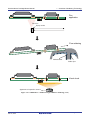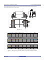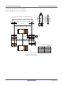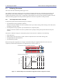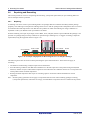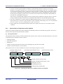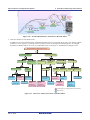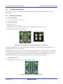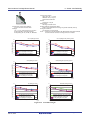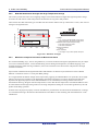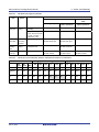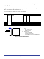
1
User’s Manual Semiconductor Package Mount Manual www.renesas.com Rev.5.00 Feb 2015 Notice 1. Descriptions of circuits, software and other related information in this document are provided only to illustrate the operation of semiconductor products and application examples. You are fully responsible for the incorporation of these circuits, software, and information in the design of your equipment. Renesas Electronics assumes no responsibility for any losses incurred by you or third parties arising from the use of these circuits, software, or information. 2. Renesas Electronics has used reasonable care in preparing the information included in this document, but Renesas Electronics does not warrant that such information is error free. Renesas Electronics assumes no liability whatsoever for any damages incurred by you resulting from errors in or omissions from the information included herein. 3. Renesas Electronics does not assume any liability for infringement of patents, copyrights, or other intellectual property rights of third parties by or arising from the use of Renesas Electronics products or technical information described in this document. No license, express, implied or otherwise, is granted hereby under any patents, copyrights or other intellectual property rights of Renesas Electronics or others. 4. You should not alter, modify, copy, or otherwise misappropriate any Renesas Electronics product, whether in whole or in part. Renesas Electronics assumes no responsibility for any losses incurred by you or third parties arising from such alteration, modification, copy or otherwise misappropriation of Renesas Electronics product. 5. Renesas Electronics products are classified according to the following two quality grades: “Standard” and “High Quality”. The recommended applications for each Renesas Electronics product depends on the product’s quality grade, as indicated below. “Standard”: Computers; office equipment; communications equipment; test and measurement equipment; audio and visual equipment; home electronic appliances; machine tools; personal electronic equipment; and industrial robots etc. “High Quality”: Transportation equipment (automobiles, trains, ships, etc.); traffic control systems; anti-disaster systems; anticrime systems; and safety equipment etc. Renesas Electronics products are neither intended nor authorized for use in products or systems that may pose a direct threat to human life or bodily injury (artificial life support devices or systems, surgical implantations etc.), or may cause serious property damages (nuclear reactor control systems, military equipment etc.). You must check the quality grade of each Renesas Electronics product before using it in a particular application. You may not use any Renesas Electronics product for any application for which it is not intended. Renesas Electronics shall not be in any way liable for any damages or losses incurred by you or third parties arising from the use of any Renesas Electronics product for which the product is not intended by Renesas Electronics. 6. You should use the Renesas Electronics products described in this document within the range specified by Renesas Electronics, especially with respect to the maximum rating, operating supply voltage range, movement power voltage range, heat radiation characteristics, installation and other product characteristics. Renesas Electronics shall have no liability for malfunctions or damages arising out of the use of Renesas Electronics products beyond such specified ranges. 7. Although Renesas Electronics endeavors to improve the quality and reliability of its products, semiconductor products have specific characteristics such as the occurrence of failure at a certain rate and malfunctions under certain use conditions. Further, Renesas Electronics products are not subject to radiation resistance design. Please be sure to implement safety measures to guard them against the possibility of physical injury, and injury or damage caused by fire in the event of the failure of a Renesas Electronics product, such as safety design for hardware and software including but not limited to redundancy, fire control and malfunction prevention, appropriate treatment for aging degradation or any other appropriate measures. Because the evaluation of microcomputer software alone is very difficult, please evaluate the safety of the final products or systems manufactured by you. 8. Please contact a Renesas Electronics sales office for details as to environmental matters such as the environmental compatibility of each Renesas Electronics product. Please use Renesas Electronics products in compliance with all applicable laws and regulations that regulate the inclusion or use of controlled substances, including without limitation, the EU RoHS Directive. Renesas Electronics assumes no liability for damages or losses occurring as a result of your noncompliance with applicable laws and regulations. 9. Renesas Electronics products and technology may not be used for or incorporated into any products or systems whose manufacture, use, or sale is prohibited under any applicable domestic or foreign laws or regulations. You should not use Renesas Electronics products or technology described in this document for any purpose relating to military applications or use by the military, including but not limited to the development of weapons of mass destruction. When exporting the Renesas Electronics products or technology described in this document, you should comply with the applicable export control laws and regulations and follow the procedures required by such laws and regulations. 10. It is the responsibility of the buyer or distributor of Renesas Electronics products, who distributes, disposes of, or otherwise places the product with a third party, to notify such third party in advance of the contents and conditions set forth in this document, Renesas Electronics assumes no responsibility for any losses incurred by you or third parties as a result of unauthorized use of Renesas Electronics products. 11. This document may not be reproduced or duplicated in any form, in whole or in part, without prior written consent of Renesas Electronics. 12. Please contact a Renesas Electronics sales office if you have any questions regarding the information contained in this document or Renesas Electronics products, or if you have any other inquiries. (Note 1) “Renesas Electronics” as used in this document means Renesas Electronics Corporation and also includes its majorityowned subsidiaries. (Note 2) “Renesas Electronics product(s)” means any product developed or manufactured by or for Renesas Electronics. (2012.4) Table of Contents 1. Overview of Soldering Technology ................................................................................................. 1 1.1 Soldering Methods .................................................................................................................................................... 2 1.1.1 Types of Soldering Method ............................................................................................................................ 2 1.1.2 Features of the Different Soldering Methods ................................................................................................. 3 1.1.3 Partial Heat Methods ...................................................................................................................................... 4 1.1.4 Total Heating Methods ................................................................................................................................... 6 1.1.5 Adaptation by Package Types ...................................................................................................................... 11 1.1.6 Solder Mounting Processes .......................................................................................................................... 12 1.1.7 Basic Mounting Processes ............................................................................................................................ 12 1.1.8 Single-sided Soldering ................................................................................................................................. 13 1.1.9 Double-sided Soldering ................................................................................................................................ 17 2. Printed Wiring Board Design......................................................................................................... 25 2.1 Lead-Type SMDs .................................................................................................................................................... 25 2.1.1 Pin Location Range for Lead-Type SMDs ................................................................................................... 26 2.1.2 Dimensional Examples for Different Package Types................................................................................... 27 2.2 Ball-Type SMD (Including LGA) Packages ........................................................................................................... 36 2.2.1 Pin Positions (Areas) for Ball-Type SMD Packages .................................................................................... 36 2.2.2 Mounting Pad Design for BGA and LGA Packages .................................................................................... 37 2.2.3 Mounting Pad Dimensions (Design Range) ................................................................................................. 37 2.3 THDs....................................................................................................................................................................... 38 2.3.1 THD Pin Location Range ............................................................................................................................. 38 2.3.2 Through Hole Diameter Design ................................................................................................................... 40 2.3.3 Through Hole Diameter Dimensional Design for Printed Wiring Boards (Design Ranges) ........................ 40 2.4 Discrete Devices ..................................................................................................................................................... 41 2.5 Board Materials ....................................................................................................................................................... 41 2.5.1 Preventing Mounting Pad Oxidation ............................................................................................................ 42 2.5.2 Printed Wiring Board Warping .................................................................................................................... 43 2.5.3 Solder Joint Reliability ................................................................................................................................. 43 3. Mounting Processes ....................................................................................................................... 45 3.1 Solder Supply Processes ......................................................................................................................................... 45 3.1.1 Solder Paste .................................................................................................................................................. 45 3.1.2 Solder Paste Printing Processes .................................................................................................................... 48 3.1.3 Amount of Solder Paste Supplied ................................................................................................................ 50 3.2 Component Mounting Processes ............................................................................................................................. 55 3.2.1 Adhesives ..................................................................................................................................................... 55 3.2.2 Component Placement Equipment ............................................................................................................... 55 3.2.3 Self-Alignment Effect .................................................................................................................................. 56 3.3 Soldering Processes ................................................................................................................................................ 64 3.3.1 The Temperature Profile Concept ................................................................................................................ 64 3.3.2 Temperature Profile Conditions ................................................................................................................... 65 3.3.3 Notes on BGA Package Reflow Soldering ................................................................................................... 67 3.3.4 Temperature Distributions in Mixed Mounting............................................................................................ 68 3.4 Cleaning Process ..................................................................................................................................................... 70 3.4.1 Flux Selection............................................................................................................................................... 71 3.4.2 Cleaning Fluid Selection .............................................................................................................................. 71 3.4.3 Selecting the Cleaning Method and Equipment ........................................................................................... 72 3.4.4 Assessment Methods .................................................................................................................................... 73 3.5 Inspection Process ................................................................................................................................................... 74 3.5.1 Visual Inspection Equipment ....................................................................................................................... 75 3.6 3.5.2 Visual Inspection Items ................................................................................................................................ 76 Repairing and Reworking ....................................................................................................................................... 78 3.6.1 Repairing ...................................................................................................................................................... 78 3.6.2 Reworking .................................................................................................................................................... 79 4. Notes on Storage and Mounting .................................................................................................... 85 4.1 Solderability ............................................................................................................................................................ 85 4.1.1 Plating Composition ..................................................................................................................................... 85 4.1.2 Solderability Evaluation Method.................................................................................................................. 86 4.1.3 Plating Thickness ......................................................................................................................................... 87 4.1.4 Wetting Time Temperature Dependence...................................................................................................... 88 4.1.5 Solderability following High-Temperature Storage ..................................................................................... 89 4.1.6 Solderability following Long-Term Storage ................................................................................................ 90 4.2 Package Storage Conditions.................................................................................................................................... 92 4.2.1 Storage Before Opening Moisture-Proof Packing ........................................................................................ 92 4.2.2 Storage After Opening Moisture-Proof Packing .......................................................................................... 92 4.2.3 Baking .......................................................................................................................................................... 93 4.2.4 Reflow Cycles .............................................................................................................................................. 93 4.3 Soldering Temperature Profiles .............................................................................................................................. 94 4.3.1 Heat Resistance Profiles ............................................................................................................................... 94 4.3.2 Heat Resistance Temperature Profile Symbols ............................................................................................ 95 4.3.3 Soldering Temperature ............................................................................................................................... 102 4.3.4 Package Contact and Pin Plating Metal Compositions............................................................................... 103 4.3.5 Notes on Solder Shorts and Opens ............................................................................................................. 103 4.4 Temperature Conditions on Second Reflow ......................................................................................................... 104 4.5 Mechanical Strength of Soldered Sections After Mounting.................................................................................. 104 5. Examples of Mounting and Problems .......................................................................................... 105 5.1 BGA Mounting Process ........................................................................................................................................ 105 5.1.1 Notes on Lead-Free Solder Mounting ........................................................................................................ 105 5.1.2 Notes on WLBGA Usage ........................................................................................................................... 106 5.1.3 Mounting Example (WLBGA) ................................................................................................................... 106 5.1.4 Examples of Problems in BGA Mounting .................................................................................................. 109 5.2 LGA Mounting Process ........................................................................................................................................ 119 5.2.1 Mounting Case (FLGA) ............................................................................................................................. 119 5.2.2 LGA Problem Cases ................................................................................................................................... 122 5.3 Notes on Mounting Pad Design for HQFP and HLQFP Mounting....................................................................... 124 5.3.1 Mounting Pad Design Example for HLQFP Mounting .............................................................................. 124 5.4 Lead-Free Solder Mounting Examples ................................................................................................................. 125 5.4.1 External Appearance of Pins Plated with Lead-Free Solder (Lead-Type) ................................................. 125 5.4.2 Cross Sectional Photographs after Mounting of Pins Plated with Lead-Free Solder (Lead-Type) ........... 126 6. Solder Joint Reliability ................................................................................................................ 127 6.1 Influence of Reflow Soldering Temperature ......................................................................................................... 127 6.1.1 Ball-type SMD ........................................................................................................................................... 127 6.1.2 Lead-type SMD .......................................................................................................................................... 128 6.2 Influence of Printed Wiring Board Thickness....................................................................................................... 129 6.3 Influence of Printed Wiring Board Materials (1) .................................................................................................. 129 6.4 Influence of Printed Wiring Board Materials (2) .................................................................................................. 130 6.5 Influence of Printed Wiring Board Pad Structure ................................................................................................. 130 6.6 Single-Sided and Double-Sided Mounting ........................................................................................................... 131 6.7 Combinations of Package Lead Pin Plating and Solder Materials ........................................................................ 132 6.8 Combinations of Package Ball Pin and Solder Materials...................................................................................... 133 6.9 Mechanical Strength ............................................................................................................................................. 134 6.9.1 QFP Lead Connection Strength .................................................................................................................. 134 6.9.2 BGA Ball Attachment Strength after High-Temperature Storage .............................................................. 136 6.9.3 Measures to Improve Resistance to Mechanical Shock ............................................................................. 136 6.10 Migration .............................................................................................................................................................. 138 7. Appendix ...................................................................................................................................... 139 7.1 Characteristics of Constituent Materials ............................................................................................................... 139 7.1.1 Thermal Expansion Coefficients of Constituent Materials ........................................................................ 139 Semiconductor Package Mount Manual R50ZZ0003EJ0500 Rev. 5.00 Feb 03, 2015 1. Overview of Soldering Technology The electronics industry is seeing ever strong demands for increasing functionality and smaller and thinner form factors in end products. At the same time, there are continuing demands for lower costs, and these demands are only expected to get stronger with time. The technologies used for mounting devices (packages) are critical for responding to these demands and a wide range of techniques and processes have been studied and applied. As an example, figure 1.1 shows the technologies required in typical solder mounting. This chapter presents an overview of solder mounting methods (and equipment) and processes. Design Printed wiring board design Conductor pattern design (including mounting pad design) Printed wiring boards Main components Surface mounting device ICs (SMD) Peripheral and chip components Parts and materials Solder paste, pre-solder materials Supplementary materials Solder mounting technologies Equipment Mounting processes Flux, adhesives Cleansers Solder printing equipment Component placement equipment Soldering equipment Cleaning equipment Other equipment (e.g. solder inspection and reworking equipment) Solder supply processes Component placement processes Soldering processes Cleaning processes Other processes (e.g. solder inspection and reworking) Figure 1.1 Solder Mounting Technologies R50ZZ0003EJ0500 Rev. 5.00 Feb 03, 2015 Page 1 of 140 1 Overview of Soldering Technology 1.1 Soldering Methods 1.1.1 Types of Soldering Method Semiconductor Package Mount Manual Soldering methods are broadly divided into two types: the partial heating method and the total heating method. Partial heating method: Heat is applied to the package leads and/or PWB in a localized manner. [Types] There are four types of soldering methods: 1. 2. 3. 4. Soldering iron Hot air Laser Pulse heating [Feature] Partial heating involves less heat stress on the device and printed wiring board, but is unsuitable for large volume production. Therefore, this method is mainly used to correct soldering or for devices with a low heat resistance. Total heating method: Heat is applied to the entire package and/or PWB. [Types] There are two types of soldering methods: 1. 2. 3. 4. 5. Infrared reflow Convection reflow Infrared convection combined VPS (Vapor Phase Soldering) Flow (wave) soldering [Feature] Because of excellence in productivity and running cost, these types are widely used. However, this method can place considerable heat stress on the semiconductor device and board. Select the soldering method best suited to your application by taking into consideration the advantages and disadvantages of each soldering method, as well as the heat resistance of the SMD. Page 2 of 140 R50ZZ0003EJ0500 Rev. 5.00 Feb 03, 2015 Semiconductor Package Mount Manual 1.1.2 1 Overview of Soldering Technology Features of the Different Soldering Methods Table 1.1 lists the features of each method. Furthermore, sections 1.1.3 and 1.1.4 discuss the partial heating methods and the total heating methods. Table 1.1 Soldering Method Features Soldering (Heating) Method Type Partial (Local) Heating Total Heating Features Method Strengths Temperature variations: large Running costs: high Temperature variations: large Running costs: high Not appropriate for mass production (long processing times) All pins and all components must be heated Not appropriate for mass production (long processing times) All pins and all components must be heated Temperature variations: large Processing times: short Thermal stress: high Simple structures It is difficult to heat components that are in shadows Temperature variations arise due to component shapes and colors (for near-IR) Soldering iron method Thermal stress: low Hot air method Thermal stress: low Laser method Thermal stress: low Post-soldering is possible Pulse heating method Thermal stress: low Post-soldering is possible Infrared method (IR reflow) Running costs: low Convection method (convection reflow) Weaknesses Temperature variations: medium Thermal stress: high Direct heating of high density parts and parts that are in shadows is easy Processing times: somewhat longer than those for IR reflow soldering Even heating is possible An even temperature distribution is reached after a certain amount of time even if the board and components have different thermal capacities. Component displacement and board vibrations can occur due to the flow speed. Air Running costs: low Solder defects due to copper foil oxidation can occur N2 It is difficult for solder defects due to copper foil oxidation to occur. Running costs: high Combined IR/ convection method Temperature variations: medium Thermal stress: high Processing times: short Direct heating of high density parts and parts that are in shadows is easy Component displacement and board vibrations can occur due to the flow speed. Even heating is possible Solder defects due to copper foil oxidation can occur (for convection reflow soldering) An even temperature distribution is reached after a certain amount of time even if the board and components have different thermal capacities. Air Running costs: low Solder defects due to copper foil oxidation can occur N2 It is difficult for solder defects due to copper foil oxidation to occur. Running costs: high VPS (vapor phase soldering) Flow soldering (wave soldering) Temperature variations: small Thermal stress: high Precise temperature control is possible Running costs: high No temperature control system is required Equipment costs: high The heating temperature can be made lower and the time shorter Minimal oxidation and contamination of soldered sections Running costs: low Temperature variations: large Processing times: short Thermal stress: low (THD) Handling diverse packages (such as fine lead pitch packages) is difficult Thermal stress: high (SMD) R50ZZ0003EJ0500 Rev. 5.00 Feb 03, 2015 Page 3 of 140 1 Overview of Soldering Technology 1.1.3 (1) Semiconductor Package Mount Manual Partial Heat Methods Soldering Iron Method In this method, the package leads are soldered to the mounting pads on the printed wiring board using a soldering iron and wire solder. The thermal capacity of the soldering iron used must be determined based on the size and shapes of the places to be soldered and the melting point of the solder. Care is required, since increasing the temperature more than necessary can lead to degradation due to exceeding heat tolerances, for example peeling of the mounting pads from the printed wiring board. Since the actual temperatures of the places soldered depend on the heating capacity of the soldering iron (the heat source) and the thermal capacities of the package and mounting board, it is necessary to take these issues into account by, for example, measuring thermal characteristics before starting work. Also, soldering irons with temperature adjustments should be used if at all possible. Solder Soldering iron Figure 1.2 Soldering Iron Method (2) Hot Air Soldering This method solders the SMD by heating air or N2 gas with a heater and flowing hot gas from a nozzle onto the joint on the PWB. The temperature is adjusted by adjusting the heat source and/or the flow of gas. Air Heater Hot air Solder Nozzle Figure 1.3 Hot Air Method Page 4 of 140 R50ZZ0003EJ0500 Rev. 5.00 Feb 03, 2015 Semiconductor Package Mount Manual (3) 1 Overview of Soldering Technology Laser Method In this method, devices are soldered by heating with a laser beam. The temperature is adjusted by adjusting the intensity of the laser output and by changing the heating time. Laser beam Heat Solder Figure 1.4 Laser Method (4) Pulse Heating Method In this method, the Joule heating that occurs due to a current pulse in the tool is used for soldering. The temperature is adjusted by adjusting the amount of current and the time for which the current is applied. Cable Pulse heating tool Pulse current Joule heating Figure 1.5 Pulse Heating Method R50ZZ0003EJ0500 Rev. 5.00 Feb 03, 2015 Page 5 of 140 1 Overview of Soldering Technology 1.1.4 Semiconductor Package Mount Manual Total Heating Methods Total heating methods include infrared methods, VPS (vapor phase soldering), and convection methods. These methods differ in the path over which heat is applied as shown below. Radiative heating Conductive heating Vapor phase heating Conductive heating Printed wiring board BGA Infrared methods Convective heating Conductive heating VPS Convection methods Figure 1.6 Heat Transmission Paths for Different Heating Methods As can clearly be seen from the transmission paths, for IR methods (IR reflow), soldering sections that are in the package shadow are heated indirectly by transmission heating. Since it is easy for uneven temperatures to occur, convection methods (air or N2 reflow) are mostly used when soldering is performed in the areas under packages such as BGA and LGA packages. Users must establish mounting (heating) conditions that allow adequate solder wetting of all pins to assure adequate connection strength and reliability. Figure 1.7 shows cross sectional photographs of solder joints for representative packages mounted with a Sn-3.0Ag0.5Cu solder. 100 pin QFP 28 pin QFN 261 pin BGA 64 pin LGA 0.5 mm pitch 0.5 mm pitch 0.65 mm pitch 0.65 mm pitch Figure 1.7 Post-Mounting Cross Sectional Photographs for Representative Packages Using a Sn-3.0Ag-0.5Cu Solder Page 6 of 140 R50ZZ0003EJ0500 Rev. 5.00 Feb 03, 2015 Semiconductor Package Mount Manual (1) 1 Overview of Soldering Technology IR Method (IR Reflow) In this method, components are heated by emitted IR radiation (radiative heating) using an IR heater as the heat source. Since the radiative efficiency for IR heating differs with the structural materials and the shape of the components, temperature differences arise due to differences between the packages (devices). IR reflow soldering has the following characteristics. 1. Advantages Superlative running costs and ease of maintenance Short soldering times 2. Disadvantages The pin temperature increase depends strongly on the package size. It is difficult to raise the temperature of areas in shadows where the IR radiation does hit. As a result of the above two phenomena, it is easy for differences in temperature to arise in the printed wiring board and components (places being soldered). As a result, it is necessary to set process conditions based on the places that are the most difficult to heat, and there is a tendency for large thermal stresses to be applied to packages. IR heater IR rays (radiative heating) Figure 1.8 IR Method (Example) R50ZZ0003EJ0500 Rev. 5.00 Feb 03, 2015 Page 7 of 140 1 Overview of Soldering Technology (2) Semiconductor Package Mount Manual VPS (Vapor Phase Soldering Method) In this method, a special inert liquid is heated by a heater and the product to be soldered is immersed in the saturated vapor atmosphere acquired by the boiling of that liquid, and the vapor that contacts the product releases its latent heat of vaporation as it condenses. This results in highly efficient and even soldering of the product. Figure 1.9 shows the structure of the equipment used in this method. This equipment consists of the first vapor phase used for the batch reflow soldering, a preheater, cooling, and a second vapor phase to prevent splashing of the liquid from the first vapor phase. Vapor phase soldering has the following characteristics. 1. Advantages The efficiency with which heat is transmitted to the work is extremely high and the whole work is heated evenly regardless of the shapes of the components. Since the latent heat of vaporation is used, the temperature can be controlled precisely. Since soldering is performed in an inert atmosphere, there is minimal oxidation or contamination of the soldered sections. As a result of the above features, the heating conditions can be kept low and the processing times can be short. As a result, the thermal stress applied to the packages is minimal. 2. Disadvantages High running costs. Conveyor Second cooling coil Second vapor phase First cooling coil First vapor phase Heater Inert liquid (boiling) Figure 1.9 Vapor Phase Soldering Method (Example) Page 8 of 140 R50ZZ0003EJ0500 Rev. 5.00 Feb 03, 2015 Semiconductor Package Mount Manual (3) 1 Overview of Soldering Technology Convection Reflow Method (Air or N2 Reflow) This is a method that resolves the problems of uneven heating of the printed wiring board and components in IR reflow and of high running costs of VPS (see section 1.1.4 (2)). The basic principle of convection reflow soldering is that an atmosphere (air or N2) heated by a heater is circulated within a furnace and heat is transmitted to the work by convection heating to perform the soldering. The result of this process is that an even temperature distribution is achieved after a fixed time even if there are differences in thermal capacities between the board and components. Convection reflow (hot air) soldering has the following characteristics. 1. Advantages Superlative temperature evenness compared to IR methods (IR reflow). (The temperature is not significantly affected by the objects being heated.) Comparatively low thermal stress. 2. Disadvantages The soldering time tends to be longer than that for IR reflow. Heater Fan Straightening vanes Heated air Figure 1.10 Convection Reflow Method (Example) (4) Combined Convection IR Method (Convection/IR Reflow) In this method, convection and IR heating are combined to decrease the soldering time, which is a disadvantage of the previous method (convection reflow). Fan Heater Straightening vanes Heated air IR rays Figure 1.11 Convection Reflow Method (Example) R50ZZ0003EJ0500 Rev. 5.00 Feb 03, 2015 Page 9 of 140 1 Overview of Soldering Technology (5) Semiconductor Package Mount Manual Flow (Wave Soldering) Method In this method, solder melted in a tank flows onto the work to perform the soldering. The printed wiring board is immersed in the flowing melted solder. This method has the following characteristics. 1. Advantages It is superb for mass production (soldering can be completed in a few seconds). 2. Disadvantages It is difficult to use with diverse package types, especially ball type SMD packages and narrow lead pitch SMD packages. THD Chip component Flowing solder (second wave) Flowing solder (first wave) Lead type SMD Melted solder Melted solder Figure 1.12 Flow (Wave Soldering) Method (Example) Page 10 of 140 R50ZZ0003EJ0500 Rev. 5.00 Feb 03, 2015 Semiconductor Package Mount Manual 1.1.5 1 Overview of Soldering Technology Adaptation by Package Types Available soldering methods due to package type. An example where soldering methods are classified by package is shown below. Select the soldering method best suited to your application by taking into consideration the advantages and disadvantages of each soldering method, as well as the heat resistance of the parts. Table 1.2 Soldering Method Applicability by Package Type Soldering Method SIP DIP SDIP SOP SSOP HSOP QFP LQFP HQFP HLQFP TQFP HTQFP TSOP HTSOP TSSOP VSSOP P-VSON HSOI G-QFP Total IR, convection, Heating and combined reflow VPS QFN P-VQFN BGA LFBGA HBGA HFBGA TFBGA LGA Soldering iron Partial Heating Hot air (Local Laser Heating) Pulse heater QFJ SOJ MFPAK SMPAK CMPAC SMFPAK TSOP-6 LDPAK(S) *4 LFPAK G-QFJ *5 HQFP*4 HLQFP*4 HTQFP*4 HSOP*4 HTSOP*4 HTSSOP*4 HSOI*4 HQFN*4 RP8P*4 SFP DPAK(S)*4 and other discrete packages *5 Wave soldering*3 *1 *1*2 : Applicable : Not applicable (This combination should be avoided) Notes: 1. 2. 3. 4. 5. Pin pitch (mm) Soldering 1.27 1.0 0.8 Applicable 0.65 0.5 0.4 Problematic The ability to withstand heat differs between individual semiconductor products. Contact your Renesas sales representative for details. There are also certain products for which the maximum solder tank temperature is 235°C and the maximum solder tank pass-through time is 5 seconds. Solder bridges and other problems may occur with fine pitch devices. Only use this combination after verifying mountability. Exposed heat spreader and exposed die pad types Avoid heating heat spreaders (or die pads) with the soldering iron. R50ZZ0003EJ0500 Rev. 5.00 Feb 03, 2015 Page 11 of 140 1 Overview of Soldering Technology 1.1.6 Semiconductor Package Mount Manual Solder Mounting Processes Solder mounting processes can be classified into those that support printed wiring boards with components mounted on only one side and those that support printed wiring boards with components mounted on both sides. Also, packages mounted on printed wiring board can be classified into lead insertion types (THD) and surface mounting types (SMD). Since there are soldering processes that are appropriate for each of these, there are basically six types of process. 1.1.7 Basic Mounting Processes Single-sided mounting (1) THD flow soldering (2) SMD flow soldering (3) SMD reflow soldering Double-sided mounting (1) SMD reflow soldering + THD/SMD flow soldering (2) SMD reflow soldering + SMD reflow soldering (3) THD/SMD flow soldering Figures 1.13 to 1.18 on the following pages present simplified views of these processes. In mixed mounting, in which multiple packages of differing types are mounted on the same printed wiring board, the ability to withstand heating of the different devices must be taken into consideration when determining the optimal mounting process. Page 12 of 140 R50ZZ0003EJ0500 Rev. 5.00 Feb 03, 2015 Semiconductor Package Mount Manual 1.1.8 (1) 1 Overview of Soldering Technology Single-sided Soldering Flow Soldering of THD THD Printed wiring board Inseration of component Flux application Flux Spray nozzle Flow soldering Melted solder Solder port Visual check Appearance inspection camera Figure 1.13 THD Flow Soldering R50ZZ0003EJ0500 Rev. 5.00 Feb 03, 2015 Page 13 of 140 1 Overview of Soldering Technology (2) Semiconductor Package Mount Manual Flow Soldering of SMD Adhesive application Adhesive Printed wiring board Lead type SMD Mounting of component Heat Adhesive - thermal hardening Flux application Flux Spray nozzle Figure 1.14 SMD Flow Soldering Page 14 of 140 R50ZZ0003EJ0500 Rev. 5.00 Feb 03, 2015 Semiconductor Package Mount Manual 1 Overview of Soldering Technology Flow soldering Melted solder Solder port Appearance inspection camera Visual check Figure 1.14 SMD Flow Soldering (cont.) R50ZZ0003EJ0500 Rev. 5.00 Feb 03, 2015 Page 15 of 140 1 Overview of Soldering Technology (3) Semiconductor Package Mount Manual Reflow Soldering of SMD Lead type SMD Ball type SMD Solder inspection camera Solder paste Solder printing and inspection Printed wiring board Solder paste Ball type SMD (BGA) Lead type SMD Mounting of component Heat Heat Convection heating (air/N2 reflow) Appearance inspection camera Visual check (SMDs only) Figure 1.15 SMD Reflow Soldering Page 16 of 140 R50ZZ0003EJ0500 Rev. 5.00 Feb 03, 2015 Semiconductor Package Mount Manual 1.1.9 (1) 1 Overview of Soldering Technology Double-sided Soldering SMD Reflow + THD/SMD Flow Soldering Solder inspection camera Solder printing and inspection Printed wiring board Solder paste Lead type SMD Mounting of component Heat Convection heating (air/N2 reflow) Appearance inspection camera Visual check Figure 1.16 SMD Reflow + THD/Lead-Type SMD Flow Soldering R50ZZ0003EJ0500 Rev. 5.00 Feb 03, 2015 Page 17 of 140 1 Overview of Soldering Technology Semiconductor Package Mount Manual Board inversion Adhesive application Adhesive Chip component Mounting of component Heat Adhesive - thermal hardening THD Board reversal and component mounting (insertion) Figure 1.16 SMD Reflow + THD/Lead-Type SMD Flow Soldering (cont.) Page 18 of 140 R50ZZ0003EJ0500 Rev. 5.00 Feb 03, 2015 Semiconductor Package Mount Manual 1 Overview of Soldering Technology Flux application Flux Spray nozzle Flow soldering Melted solder Solder port Visual check Appearance inspection camera Figure 1.16 SMD Reflow + THD/Lead-Type SMD Flow Soldering (cont.) R50ZZ0003EJ0500 Rev. 5.00 Feb 03, 2015 Page 19 of 140 1 Overview of Soldering Technology (2) Semiconductor Package Mount Manual SMD Reflow + SMD Reflow Soldering Solder inspection camera Solder printing and inspection Printed wiring board Solder paste Lead type SMD Mounting of component Heat Convection heating (air/N2 reflow) Appearance inspection camera Visual check Figure 1.17 SMD Reflow + SMD Reflow Soldering Page 20 of 140 R50ZZ0003EJ0500 Rev. 5.00 Feb 03, 2015 Semiconductor Package Mount Manual 1 Overview of Soldering Technology Solder inspection camera Board reversal, Solder printing, and inspection Ball type SMD (BGA) Mounting of component Heat Convection heating (air/N2 reflow) Figure 1.17 SMD Reflow + SMD Reflow Soldering (cont.) R50ZZ0003EJ0500 Rev. 5.00 Feb 03, 2015 Page 21 of 140 1 Overview of Soldering Technology (3) Semiconductor Package Mount Manual THD/Lead-Type SMD Flow Soldering Adhesive application Adhesive Printed wiring board Lead type SMD Chip component Mounting of component Heat Adhesive - thermal hardening THD Board reversal and component mounting (insertion) Figure 1.18 THD/Lead-Type SMD Flow Soldering Page 22 of 140 R50ZZ0003EJ0500 Rev. 5.00 Feb 03, 2015 Semiconductor Package Mount Manual 1 Overview of Soldering Technology Flux application Flux Spray nozzle Flow soldering Melted solder Solder port Visual check Appearance inspection camera Figure 1.18 THD/Lead-Type SMD Flow Soldering (cont.) R50ZZ0003EJ0500 Rev. 5.00 Feb 03, 2015 Page 23 of 140 1 Overview of Soldering Technology Page 24 of 140 Semiconductor Package Mount Manual R50ZZ0003EJ0500 Rev. 5.00 Feb 03, 2015 Semiconductor Package Mount Manual 2 Printed Wiring Board Design 2. Printed Wiring Board Design 2.1 Lead-Type SMDs In designing the mounting pads for a printed wiring board that mounts lead-type SMD packages, it is important to take the shape of the leads into consideration. Also note that care is required, since there may be subtle differences in pin shapes even between devices with the same package name. The parameters regulating the mount pad dimensions are as follows. Cleanliness: Soldering strength: 1 Pattern precision and ease of visual inspection: 2 Solder bridge tolerance: The allowable margins for which are determined by the pattern design philosophy and the device's application. Below, we describe the design method for the printed wiring board mounting pad dimensions and pin position precision based on package drawings. R50ZZ0003EJ0500 Rev. 5.00 Feb 03, 2015 Page 25 of 140 2 Printed Wiring Board Design 2.1.1 Semiconductor Package Mount Manual Pin Location Range for Lead-Type SMDs The package pin positions (pin location range), which are critical when designing the mounting pads on a printed wiring board, are stipulated in terms of the tolerances for the pin widths and the pin center positions in the package drawing. For the pin center position tolerance, the maximum material condition can be expressed as follows. M Symbol : This symbol expresses the positional tolerance Symbol : This symbol expresses the tolerance zone for the pin center position Symbol M : This symbol expresses the maximum material condition. That is, the tolerance zone (range) for the pin center position allowed when the pin width is maximum. The true pin location range is the range from the true center position to the maximum pin width. However, since the pin center position also has a tolerance, the maximum pin location range is the sum of the maximum pin width and the pin center position tolerance zone. The maximum material condition expresses the fact that the maximum pin location range (the maximum allowable range for a pin) shown above cannot be exceeded regardless of the pin width. Therefore, when the pin width is narrower than the maximum pin width, the tolerance for the pin center position will be larger. In the following, we present an example based on a 0.5 mm pitch QFP. Pin width = 0.2 0.05 mm Tolerance zone for the pin center position = φ0.08 M Thus for a 0.5 mm pitch QFP, the maximum pin location range will be 0.33 mm (±0.165 mm) from the true pin center position. True center position Tolerance zone for the pin center position: X = 0.08 mm (0.04 mm) Maximum pin location range = pin maximum width + tolerance zone for the pin center position = 0.25 + 0.08 = 0.33 Pin center position tolerance: pin position for +0.04 mm tolerance Pin center position tolerance: pin position for -0.04 mm tolerance 0.25 mm Pin maximum width (true pin location range) 0.33 mm Maximum pin location range (the maximum allowable range for a pin) Figure 2.1 Pin Center Position Tolerance for a 0.5 mm Pitch QFP Page 26 of 140 R50ZZ0003EJ0500 Rev. 5.00 Feb 03, 2015 Semiconductor Package Mount Manual 2.1.2 2 Printed Wiring Board Design Dimensional Examples for Different Package Types (1) Gull Wing Type Packages [1] SOP (MIL standard) ................................................................................................................................. Figure 2.2 [2] TSOP (type I, type II), SSOP, LSSOP, TSSOP, VSSOP, and WSOP...................................................... Figure 2.3 [3] QFP, HQFP, LQFP, TQFP, HLQFP, and HTQFP ................................................................................... Figure 2.4 [4] HQFP, HLQFP, and HTQFP (exposed die pad type) .............................................................................. Figure 2.5 [5] HQFP, HLQFP (Exposed back surface heat spreader type) .................................................................... Figure 2.6 (2) J-Lead Type Packages [1] SOJ .......................................................................................................................................................... Figure 2.7 [2] QFJ .......................................................................................................................................................... Figure 2.8 (3) Non-Lead Type Packages [2] QFN and HQFN ...................................................................................................................................... Figure 2.9 R50ZZ0003EJ0500 Rev. 5.00 Feb 03, 2015 Page 27 of 140 2 Printed Wiring Board Design (1) Semiconductor Package Mount Manual Gull Wing Type Package Dimensions [1] Mounting pad dimensions for SOP (MIL standard) packages The mounting dimensions are those shown below. e β2 L β1 α α γ β1 L β2 b2 b e b2 l2 e1 l2 = L + β1 + β2 b ≤ b2 ≤ e − γ The constants are all the same for the package widths Package width e1 from type 1 (225 mil) to type 6 (600 mil). e1 types — Type 1: 225 mil (5.72) Type 2: Type 3: Type 4: Type 5: Type 6: 300 mil ( 7.62) 375 mil (9.53) 450 mil (11.43) 525 mil (13.34) 600 mil (15.24) • Renesas Package Dimension Examples: SOP Type (MIL Standard) e 1.27 1.00 0.80 0.65 0.50 Constant ⎯ ⎯ ⎯ ⎯ α 0.20 and larger ⎯ ⎯ ⎯ ⎯ β1 0.20 to 0.50 ⎯ ⎯ ⎯ ⎯ β2 0.20 ⎯ ⎯ ⎯ ⎯ γ 0.30 Unit: mm 0.40 ⎯ ⎯ ⎯ ⎯ Note: Reference values based on the former EIAJ ED-7402-1 standard. Figure 2.2 SOP Type (MIL Standard) Examples Page 28 of 140 R50ZZ0003EJ0500 Rev. 5.00 Feb 03, 2015 Semiconductor Package Mount Manual 2 Printed Wiring Board Design [2] Mounting dimensions for TSOP (type I, type II), SSOP, LSSOP, TSSOP, VSSOP, and WSOP packages The mounting dimensions are those shown below. e β2 L β1 α α HE or HD β1 L β2 γ b2 b e b2 l2 l2 = L + β1 + β2 b ≤ b2 ≤ e − γ • Renesas Package Dimension Examples: TSOP type Ι Constant α β1 β2 γ e 1.27 ⎯ ⎯ ⎯ ⎯ 1.00 ⎯ ⎯ ⎯ ⎯ 0.80 ⎯ ⎯ ⎯ ⎯ 0.65 0.05 to 0.10 0.20 to 0.25 0.20 to 0.40 0.30 • Renesas Package Dimension Examples: TSOP type ΙΙ e 1.27 1.00 0.80 0.65 Constant ← ← α 0.05 to 0.10 ← ← ← β1 0.20 to 0.25 ← ← ← β2 0.20 to 0.40 ← ← ← ← γ 0.30 Unit: mm 0.55 ← ← ← 0.25 0.50 ← ← ← ← 0.40 ← ← ← 0.20 0.55 ⎯ ⎯ ⎯ ⎯ 0.50 ⎯ ⎯ ⎯ ⎯ Unit: mm 0.40 0.05 to 0.10 0.20 to 0.25 0.20 to 0.40 0.20 • Renesas Package Dimension Examples: SSOP, LSSOP, TSSOP, VSSOP, and WSOP e 1.27 1.00 0.80 0.65 0.55 0.50 ⎯ ← ⎯ 0.10 to 0.30 α 0.10 to 0.30 ← ⎯ ← ⎯ 0.20 to 0.40 β1 0.20 to 0.55 ← ⎯ ← ⎯ 0.20 to 0.40 β2 0.20 to 0.40 ← ⎯ ← ← ⎯ γ 0.30 0.25 Constant Unit: mm 0.40 ← ← ← 0.20 Note: Reference values based on the former EIAJ ED-7402 standard. Figure 2.3 TSOP (type I, type II), SSOP, LSSOP, TSSOP, VSSOP, and WSOP Examples R50ZZ0003EJ0500 Rev. 5.00 Feb 03, 2015 Page 29 of 140 2 Printed Wiring Board Design Semiconductor Package Mount Manual [3] Mounting dimensions for QFP, HQFP, LQFP, TQFP, HLQFP, and HTQFP packages The mounting dimensions are those shown below. e β2 L β1 α α HE or HD β1 L β2 b2 γ b e b2 l2 l2 = L + β1 + β2 b ≤ b2 ≤ e − γ • Renesas Package Dimension Examples: QFP and HQFP; Products with built-in heat spreaders e 1.00 0.80 0.65 Constant ← ← α 0.30 ← ← β1 0.50 ← ← β2 0.20 to 0.40 ← ← γ 0.30 0.50 0.10 to 0.30 0.20 to 0.40 ← 0.25 • Renesas Package Dimension Examples: LQFP, TQFP, HLQFP, and THQFP; Products with built-in heat spreaders Constant α β1 β2 γ e 1.00 0.10 to 0.30 0.20 to 0.40 0.20 to 0.40 0.30 0.80 ← ← ← ← 0.65 ← ← ← ← 0.50 ← ← ← 0.25 Unit: mm 0.40 ← ← ← 0.20 Unit: mm 0.40 ← ← ← 0.20 Note: Reference values based on the former EIAJ ED-7404 standard. Figure 2.4 QFP, HQFP, LQFP, TQFP, and HTQFP Examples Page 30 of 140 R50ZZ0003EJ0500 Rev. 5.00 Feb 03, 2015 Semiconductor Package Mount Manual 2 Printed Wiring Board Design [4] Mounting pad dimensions for QFP (HQFP, HLQFP, and HTQFP (exposed die pad type)) packages The mounting dimensions are those shown below. e D2 or E2 β2 L β1 α D2 β1 L β2 α HE or HD b2 γ b E2 e b2 l2 Note: For exposed die pad products where the die pad is soldered to the board, the mounting pad dimensions are equivalent to the size of the exposed die pad (E2 × D2). l2 = L + β1 + β2 b ≤ b2 ≤ e − γ • Renesas Package Dimension Examples: HQFP (Exposed Die Pad Products) e 1.00 0.80 Constant ← α 0.30 ← β1 0.50 ← β2 0.20 to 0.40 ← γ 0.30 0.65 ← ← ← ← 0.50 0.10 to 0.30 0.20 to 0.40 ← 0.25 • Renesas Package Dimension Examples: HLQFP and HTQFP (Exposed Die Pad Products) Constant α β1 β2 γ e 1.00 0.10 to 0.30 0.20 to 0.40 0.20 to 0.40 0.30 0.80 ← ← ← ← 0.65 ← ← ← ← 0.50 ← ← ← 0.25 Unit: mm 0.40 ← ← ← 0.20 Unit: mm 0.40 ← ← ← 0.20 Note: Reference values based on the former EIAJ ED-7404 standard. Figure 2.5 HQFP, HLQFP, and HTQFP Examples R50ZZ0003EJ0500 Rev. 5.00 Feb 03, 2015 Page 31 of 140 2 Printed Wiring Board Design Semiconductor Package Mount Manual [5] Mounting dimensions for HQFP and HLQFP (Exposed back surface heat spreader type) packages Mounting pad dimensions: The mounting pad dimensions are designed as shown below. PRQP0064JB-A 19.2 14.0 12.0 11.6 4-C1.0 33 48 32 0.65 45 ˚ 11.6 12.0 14.0 ** 64 17 1 2.0 19.2 49 16 0.35 PLQP0080KD-A 18.0 15.0 14.0 11.2 4−C1.50 60 41 10.4 13.2 0.5 40 15.0 14.0 11.2 * 21 1 20 1.5 80 10.4 13.2 18.0 61 0.25 PLQP0100KD-A 17.4 14.2 13.0 4−C0.7 75 76 51 50 12.0 12.0 13.2 17.4 14.2 13.0 0.5 13.2 * 100 1 25 0.25 1.4 26 Note: * We recommend setting up silk screen or solder resist features on the board to prevent solder escape during reflow to assure the required amounts of solder for the contact land areas that correspond to the heat spreader corner sections. Figure 2.6 HQFP and HLQFP (Exposed back surface heat spreader type) Examples Page 32 of 140 R50ZZ0003EJ0500 Rev. 5.00 Feb 03, 2015 Semiconductor Package Mount Manual (2) 2 Printed Wiring Board Design J-Lead Type Package Dimensions [1] Mounting pad dimensions for SOJ packages The mounting dimensions are those shown below. e e1 b2 γ b e • Renesas Dimension Example (SOJ) Unit: mm e b2 l1 l2 l1 l2 b2 1.27 1.20 2.00 0.75 Note: Reference values based on the former EIAJ ED-7406 standard. Figure 2.7 SOJ Example R50ZZ0003EJ0500 Rev. 5.00 Feb 03, 2015 Page 33 of 140 2 Printed Wiring Board Design Semiconductor Package Mount Manual [2] Mounting pad dimensions for QFJ packages The mounting dimensions are those shown below. e e1E or e1D b2 γ b e b2 l1 • Renesas Dimension Example (QFJ) Unit: mm l2 e l1 l2 b2 1.27 1.20 2.00 0.75 Note: Reference values based on the former EIAJ ED-7407 standard. Figure 2.8 QFJ Example Page 34 of 140 R50ZZ0003EJ0500 Rev. 5.00 Feb 03, 2015 Semiconductor Package Mount Manual (3) 2 Printed Wiring Board Design Non-Lead Type Package Dimensions [1] Mounting pad dimensions for QFN and HQFN packages The mounting dimensions are those shown below. Punch Type Saw Type e e E2 HE E2 b b Lp Lp D2 D2 HD D e e l2 E2 HE2 E2 E3 b2 b2 l2 D2 D2 D3 HD2 b E Lp Lp b b2 β1 b2 β2 β1 β2 Renesas Package Dimension Examples Unit: mm 0.8 0.5 0.4 l2 = L + β1 + β2 β1 0 to 0.3 0 to 0.3 0 to 0.2 b b2 e - β2 0 to 0.3 0 to 0.3 0 to 0.2 0.1 to 0.3 0.1 to 0.3 0.1 to 0.2 When die pads are soldered, the mounting lands are designed to have the same size as the exposed die pad size. Avoid mounting leads that are exposed at the package corners (die pad hanging leads) on the printed wiring board. If required, the corner land β1 dimension should be analyzed further. Figure 2.9 QFN and HQFN Examples R50ZZ0003EJ0500 Rev. 5.00 Feb 03, 2015 Page 35 of 140 2 Printed Wiring Board Design Semiconductor Package Mount Manual 2.2 Ball-Type SMD (Including LGA) Packages 2.2.1 Pin Positions (Areas) for Ball-Type SMD Packages Since, unlike the lead-type SMD packages, the pin shape for ball-type SMD packages is a circle (or sphere). Therefore the pin width and pin center position tolerances are expressed as diameters (). In the following, we present an example of a 0.5 mm pitch FBGA package. Pin width = 0.30 ±0.05 mm Pin center position tolerance zone = φ0.05 M Thus for a 0.5 mm pitch FBGA package, the maximum pin location range will be 0.40 mm from the true pin center position. True center position Tolerance zone for the pin center position: X = 0.05 mm (0.025 mm) Pin position tolerance: pin position for +0.025 mm tolerance Pin position tolerance: pin position for -0.025 mm tolerance 0.35 mm Pin maximum width (true pin location range) 0.40 mm Maximum pin location range (the maximum allowable range for a pin) Figure 2.10 Pin Center Position Tolerance for a 0.5 mm Pitch BGA Page 36 of 140 R50ZZ0003EJ0500 Rev. 5.00 Feb 03, 2015 Semiconductor Package Mount Manual 2.2.2 2 Printed Wiring Board Design Mounting Pad Design for BGA and LGA Packages There are two types of mounting pad differentiated by their structure: NSMD (non-solder mask defined) and SMD (solder mask defined). These have the corresponding characteristics listed below. The type should be determined according to the needs of the application based on these characteristics. NSMD characteristics: Since the solder joint strength is greater than that for the SMD type, these joints have a longer thermal cycle lifetime. It is easier for pad peeling or open circuits at the pad neck necks to occur due to mechanical stresses. SMD characteristics: Since the solder joint strength is lower than that for the NSMD type, these joints have a shorter thermal cycle lifetime. It is harder for pad peeling or open circuits at the pad neck necks to occur due to mechanical stresses. Note: The characteristics above apply when the land dimensions on the package and mounting pad dimensions on the printed wiring board are the same. 2.2.3 Mounting Pad Dimensions (Design Range) e φb φ b2 e φ b2 Renesas Package dimension Example (Design Range) Pin pitch (mm) Pad dimensions b2 (mm) 1.50 1.27 1.00 0.80 0.75 0.65 0.50 0.40 0.55 to 0.65 0.55 to 0.65 0.45 to 0.55 0.35 to 0.45 0.25 to 0.35 0.30 to 0.40 0.20 to 0.30 0.15 to 0.25 Figure 2.11 BGA and LGA Examples Since the stress after solder mounting is distributed evenly at the solder joint, it is commonly said that it is acceptable to design the mounting pad dimensions to have the same dimensions as the diameter of the lands on the package (BGA and LGA). Contact your Renesas sales representative for details on the package land dimensions. R50ZZ0003EJ0500 Rev. 5.00 Feb 03, 2015 Page 37 of 140 2 Printed Wiring Board Design 2.3 Semiconductor Package Mount Manual THDs For THD packages, the approach is basically the same as that for SMD packages. However, since THD devices are held in a chuck and the leads inserted in through holes (TH) provided in the printed wiring board, it is necessary to take the dimensions in the thickness direction as well as the lead width direction into account. Thus there are some differences as compared to SMD mounting. Here we describe a design example for the pin location range and pin through hole diameter based on the package drawing for an 8-pin plastic DIP (7.62 mm (300 mil)). 2.3.1 THD Pin Location Range Figure 2.12 shows the package drawing for a 7.62 mm (300 mil) pitch 8-pin plastic DIP. Figure 2.12 Package Drawing of 8-Pin Plastic DIP (7.62 mm (300 mil)) The pin location range must be within a range determined from the pin array spacing e = 2.54 mm, the pin row spacing e = 7.62 mm, the maximum value of the pin width, and the pin positional tolerance x = 0.25 mm. The tolerance for the pin center position is a particularly important value in designing the pin location range as listed in table 2.1. 1 Pin pitch e = 2.54 Pin width b = 0.50 010 Pin row spacing e = 7.62 Pin thickness c = 0.25 0.10/0.05 φ0.25 M Pin center position tolerance = 1 Table 2.1 Pin Center Position Tolerance Symbol indicating the positional tolerance. 0.25 Numerical value indicating that the positional tolerance of the pin center is in the range of x = 0.25 mm. Allowable range that each pin center can deviate from the logically accurate dimensions when parallel chucking is performed at a pin row interval of e1 = 7.62 mm for both pin rows of the DIP package. M Symbol indicating that the positional tolerance can be up to x = 0.25 mm, based on a pin width of b MAX = 0.60 mm.(i.e. If the pin width b is less than the maximum value, the tolerance will be greater than x = 0.25 mm) Location range in the pin width direction 2x [b MAX./2 + x/2] 2 [(0.50 0.1)/2 0.25/2] 2x [0.85/2] = 0.85 mm Location range in the pin thickness direction 2x [c MAX./2 x/2] 2 [(0.25 0.1)/2 0.25/2] Page 38 of 140 R50ZZ0003EJ0500 Rev. 5.00 Feb 03, 2015 Semiconductor Package Mount Manual 2 Printed Wiring Board Design 2x [0.60/2] = 0.60 mm From the results of these calculations, the location range in the pin width direction is included in the location range in the pin thickness direction. Figure 2.13 shows the location range in the pin width direction. 0.500.10 0.25 M bMAX=0.60 True center position Center position displaced to the right when b is at its maximum. Center position displaced to the left when b is at its maximum. Center position displaced when b is at its maximum. 0.25 2 0.85 Through hole diameter 0.60 2 Location range for pin width b 2.54 Figure 2.13 Relationship Between Center Position Displacement in the Pin Width Direction and Printed Wiring Board Through Holes R50ZZ0003EJ0500 Rev. 5.00 Feb 03, 2015 Page 39 of 140 2 Printed Wiring Board Design 2.3.2 Semiconductor Package Mount Manual Through Hole Diameter Design The through hole diameter is designed based on the pin location range for the THD. Through holes on printed wiring boards are circular in shape and furthermore, since the pin thickness has a tolerance, the through hole diameter must be designed to be larger by that amount. This relationship is shown in figure 2.14, and the radius of the holes in the printed wiring board that takes the pin thickness into account can be calculated as shown below. r ( x / 2 bMAX . / 2) 2 (cMAX . / 2) 2 (0.25 / 2 0.60 / 2) 2 (0.35 / 2) 2 = 0.46 (mm) C Max Therefore, the diameter of through holes in the printed wiring board is given by = 2 × r = 2 × 0.46 = 0.92 mm. r x 2 b Max 2 True center position Figure 2.14 Relationship Between the Pin Position Displacement Considering Pin Thickness and the Printed Wiring Board Through Hole Diameter If the through hole diameter on the printed wiring board is at least 0.92 mm, then the pins can be inserted without problem. The ends of pins on DIP packages usually have a tapered shape with a taper ratio of 0.2/0.5. Therefore, printed wiring boards with through holes with a diameter smaller than 0.92 mm, namely 0.8 mm (minimum), are used. Defective soldering may occur during flow mounting or other processes if the through hole diameter is too large. When designing actual mounting pads, a comprehensive review is required for all soldering conditions, including the desired pin joint strength, package/printed wiring board precision, mechanical precision of equipment in which the board will be used, and the performance of the soldering equipment. 2.3.3 Through Hole Diameter Dimensional Design for Printed Wiring Boards (Design Ranges) Table 2.2 Through Hole Diameter Examples Pin row spacing e1 (mil) Through hole diameter (inner dimension) (mm) 300 0.85 to 0.92 400 0.81 to 0.85 600 0.85 750 0.85 Note: The pin spacing e is a fixed 1.778 mm. Page 40 of 140 R50ZZ0003EJ0500 Rev. 5.00 Feb 03, 2015 Semiconductor Package Mount Manual 2.4 2 Printed Wiring Board Design Discrete Devices For mount pad dimension of discrete devices, visit the discrete packages list on our web site at http://www.renesas.com/products/package/information/discrete_name_list/index.jsp 2.5 Board Materials Board materials can be classified into two types: printed wiring board based on epoxy resins and thick film circuit substrates (ceramic substrates) that are based on alumina ceramics. The printed wiring boards used widely in consumer and industrial equipment can be classified into three types according to the purpose of the board, as listed in table 2.3. Table 2.3 Examples of Substrate Materials Type Composition Resin Printed wiring boards Board Material Features Applications Conductor Paper phenol (FR-2) boards Phenol Paper Copper foil Low cost, ease of mass production Consumer electronic equipment Paper epoxy (FR-3) boards Epoxy Paper Copper foil A board intermediate between paper phenol and glass epoxy Audio equipment Glass epoxy (FR-4) boards Epoxy Glass cloth Copper foil Superlative in electrical characteristics, resistance to moisture, and dimensional stability Consumer electronic equipment Industrial electronic equipment Environmental considerations Consumer electronic equipment Industrial electronic equipment Glass epoxy (FR-4) boards (halogen free) Epoxy (halogen free) Glass cloth Copper foil More highly elastic than ordinary FR-4 (minimal warping and flexing) Higher heat resistance than ordinary FR-4 Heat-resistant Heatglass epoxy (FR-5 resistant equivalent) boards epoxy Glass cloth Copper foil High Tg and good reliability. COB (chip on board) A low-cost type of glass polyimide. Thin form-factor applications Flexible boards Polyimide Copper foil Can be freely bent Cameras, calculators, and similar products Ceramic substrates Alumina ceramic Ag-Pd High heat resistance and high thermal conductance. Electronic equipment for automotive applications Superb reliability. When designing a board, while the board materials must be selected based on electrical characteristics, thermal dissipation, and similar properties, designers must also analyze the aspects discussed in sections 2.5.1 to 2.5.3. R50ZZ0003EJ0500 Rev. 5.00 Feb 03, 2015 Page 41 of 140 2 Printed Wiring Board Design 2.5.1 Semiconductor Package Mount Manual Preventing Mounting Pad Oxidation The conductor used to form the mounting pads on printed wiring boards is a copper foil and surface oxidation can be promoted by storage conditions or the soldering temperature. This can result in a degradation of the solderability of the mounting pads. While the processing methods listed in table 2.4 can be used to prevent this surface oxidation, since each of these has advantages and disadvantages, the method used must be selected according to the application at hand. For example, when mounting fine pitch packages for ordinary applications, Ni/Au is commonly used as a preflux for cell phone and similar applications. If a preflux is used, an appropriate one of the many types available must be chosen for the application. Also, when solder surface processing is required for fine-pitch mounting pads, it is thought that solder plating in which the solder thickness on the surface is even (has good flatness) makes it harder for positional displacements to occur in solder printing and mounting. Since the mounting pad surface processing affects ease of mounting and reliability as described above, we strongly recommend thorough evaluation when adopting these methods. Table 2.4 Mounting Pad Surface Oxidation Prevention Processing Surface Processing Method Solder leveler Preflux Rosin Water soluble Ni/Au flashing Page 42 of 140 Strengths There is no exposure of copper surfaces Long storage periods Surface processing costs are lower than with metallic surface processing (solder leveler, gold plating). Good solderability Weaknesses The amount of solder supplied during solder printing is unstable. Since the leveler and paste are not compatible, the solderability is variable. Rosin-based fluxes include VOCs (volatile solvents) Since the preflux is applied to the whole board, foreign matter can adhere to the board surface. Storage periods are shorter Does not include VOCs (volatile solvents) Surface processing costs are lower than with metallic surface processing (solder leveler, gold plating). Since the preflux is only applied to the land surfaces, it is harder for foreign matter to adhere to the board surface. Good solderability Good heat resistance High costs Good solderability Long storage periods Mounting reliability can be degraded by due to the thickness of the gold plating. Storage periods are shorter R50ZZ0003EJ0500 Rev. 5.00 Feb 03, 2015 Semiconductor Package Mount Manual 2.5.2 2 Printed Wiring Board Design Printed Wiring Board Warping Mounting problems that were thought to be due to warping of printed wiring board and packages during reflow have now been verified. (See section 5, Examples of Solder Mounting and Mounting Problems.) In addition to changing the type of board used or its thickness, the following workarounds should also be considered if there is significant warping of the printed wiring boards and problems that could be caused by that are of concern. Equalize the ratio occupied by conductor on the printed wiring board surfaces. For double-sided mounting, analyze the placement of components and minimize the difference in coefficients of thermal expansion of the front and back sides of the board. Provide a warping prevention structure during reflow (during cooling). Use a printed wiring board clamping jig and forcibly prevent warping while performing reflow soldering. Use a heat-resistant glass epoxy board. Since the type and thickness of the board used influences board warping, we recommend carefully analyzing the board specifications, including consulting with the board manufacturer, and thoroughly checking all aspects based on this evaluation. 2.5.3 Solder Joint Reliability Minimizing the difference in coefficients of thermal expansion between the printed wiring board and the packages used must be considered to assure solder joint reliability. For example, when ceramic packages are surface mounted, consider using a ceramic board with an essentially identical coefficient of thermal expansion. Also, when mounting miniature thin packages in which the ratio of the area occupied by the silicon chip itself is high (such as the TSOP, VFQN, and S-WFBGA packages), increased solder joint lifetimes can be expected if you select a board with a coefficient of thermal expansion that is as close to that of the package as possible to reduce the apparent coefficient of thermal expansion of the packages overall. Such boards include FR-5 equivalent boards that have a high glass transition temperature (Tg) and a small coefficient of thermal expansion. R50ZZ0003EJ0500 Rev. 5.00 Feb 03, 2015 Page 43 of 140 2 Printed Wiring Board Design Page 44 of 140 Semiconductor Package Mount Manual R50ZZ0003EJ0500 Rev. 5.00 Feb 03, 2015 Semiconductor Package Mount Manual 3 Mounting Processes 3. Mounting Processes 3.1 Solder Supply Processes 3.1.1 Solder Paste (1) Material Structure The main components of solder paste are solder powder and flux. The amount of solder powder contained in solder paste is generally in the 80 to 95 weight % range. The amount contained influences both the viscosity of the paste and the thickness of the solder after reflow. The following sections discuss the solder powder and the flux. a. Solder powder Previously, the metallic structure of solder powder consisted of a variety of alloys, mainly in the Sn-Pb family and the Sn-Pb-Ag family, such as eutectic solder (Sn-37Pb) and solder with added silver, such as the Sn-36Pb-2Ag solder. However in recent years, a variety of lead-free metallic compositions (mainly in the Sn-Ag-Cu family) have come to be widely used to completely eliminate lead for environmental reasons. The particular lead-free alloy used is chosen according to the application and soldering method used. Solder powder has a range of power particle sizes as shown in figure 3.1, and this range affects the printing characteristics of the solder paste. Note that solder powder with spherical shape should be used for mounting packages with a fine pin pitch. While solder powders with a particle diameter of 50 to 60 µm or smaller are commonly used, better results can be obtained for fine pitch packages (such as 0.5 mm or finer pitch QFP and 0.8 mm and finer pitch BGA packages) by using a material with a fine particle size of 40 µm or smaller and a narrow viscosity distribution. Note, however, that there is concern that, with solder powders with finer particle sizes, capillary ball formation due to surface oxidation may occur and that solder wettability may be affected. This means that special care is required when using this type of solder powder. b. Flux Flux is used for the following reasons in soldering processes. Removal of oxidized matter from components and pattern surfaces. Preventing reoxidation during soldering Reducing the surface tension of the molten solder That is, it is used to improve solderability. The four components of the fluxes used to assist soldering are tackifiers, thixotropic agents, solvents, and activating agents. These are used for the following purposes. Tackifier resins: Component mountability, metal cleaning, reoxidation prevention Thixotropic agents: Preventing separation of solder powder and flux, and droop prevention Activating agents: Metal cleaning Solvents: Forming the paste There are three main types of flux: rosin fluxes, alloy resin fluxes, and water soluble fluxes. In addition, rosin fluxes are classified into three types by their degree of activation: R (non-activated Rosin), RMA (Rosin Mildly Activated), and RA (Rosin Activated). Table 3.1 lists their features. R50ZZ0003EJ0500 Rev. 5.00 Feb 03, 2015 Page 45 of 140 3 Mounting Processes Table 3.1 Semiconductor Package Mount Manual Flux Types and Features Flux Type Features Type R, ROL Type (non-activated Rosin , Rosin Low activity levels) These are non-activated fluxes. They are noncorrosive. Type RMA, ROM Type (Rosin Mildly Activated , Rosin Moderate activity levels) These are weakly activated fluxes. They are noncorrosive. They provide superior solderability compared to type R fluxes. Type RA, ROH Type (Rosin Activated , Rosin High activity levels) These are strongly activated fluxes. While they provide superior solderability compared to type R and RMA fluxes, they are more strongly corrosive. Solder Powder Size Range Sn-3Ag-0.5Cu Solder Powder Sn-37Pb Solder Powder Type 2 0.075 mm to 0.045mm Type 3 0.045 mm to 0.020mm Type 4 0.038 mm to 0.020mm Type 5 0.025 mm to 0.010mm Figure 3.1 SEM Photographs of Solder Particles in Solder Paste Page 46 of 140 R50ZZ0003EJ0500 Rev. 5.00 Feb 03, 2015 Semiconductor Package Mount Manual Table 3.2 3 Mounting Processes Solder Powder Size for Solder Paste and Corresponding Lead Pitches Lead type packages: QFP, SOP, and similar packages Solder Powder Size Range Lead Pitch (mm) 1.27 1.00 0.80 0.65 0.50 0.40 0.075 to 0.045 mm 0.045 to 0.020 mm 0.038 to 0.020 mm 0.025 to 0.010 mm Source: Senju Metal Industry Co., Ltd. Bump and land type packages: BGA, LGA, and similar packages Solder Powder Size Range Land Pitch (mm) 1.27 1.00 0.80 0.65 0.50 0.40 0.075 to 0.045 mm 0.045 to 0.020 mm 0.038 to 0.020 mm 0.025 to 0.010 mm Source: Senju Metal Industry Co., Ltd. (2) Required Characteristics This section discusses the characteristics required in solder pastes. a. Before reflow Minimal changes with time since manufacture. Good printability and applicability characteristics. Minimal changes with time after application. (A long retention time for adhesion characteristics, and loss of shape does not occur.) The solder powder must not separate from the flux. The surface must not harden after solder paste manufacture. Minimal droop (and bleeding). b. After reflow Good solderability Minimal occurrence of capillary balls. Good cleanability characteristics, so that no flux residues remain. If flux residues do occur, reliability must be maintained. (3) Notes on Selection When selecting a solder paste, keep the following points in mind from the standpoints of printability, solder bridges and solder balls, and cleanability. a. Printability Normally, a solder powder particle size of 1/4 to 1/5 or less of the metal stencil aperture is selected. If the viscosity is too high, stencil separability is degraded and cracking/crazing can occur. If it is too low, bleeding or print drooping may occur. Generally, for printing a viscosity of from 200 to 300 Pa·s at 25°C (Malcolm solder paste viscometer) is recommended. (The thixotropic properties of the solder paste also require care.) R50ZZ0003EJ0500 Rev. 5.00 Feb 03, 2015 Page 47 of 140 3 Mounting Processes Table 3.3 Semiconductor Package Mount Manual Solder Paste Characteristics by Applications Application Viscosity (Pa·s at 25°C) Dispenser 100 to 300 Printing 200 to 300 b. Solder bridges and capillary balls Watch out for solder powder oxidation, and select a solder powder narrow particle size distribution. Select a solder paste with flux solvents that have a low boiling point, and select a solder paste in which the rosin has a high molecular weight and the amount of flux is the lowest possible. c. Cleanability Cleaning residues are thought due to reduced rosin solubility in the cleaning agents, that is caused by the rosin oxidation while the reflow process. Accordingly, select a solder paste that uses a rosin that is stable with respect to oxidation. 3.1.2 Solder Paste Printing Processes There are two supply methods for solder paste: dispenser supply and printing. Usually, printing is selected for its mass production efficiency. Therefore we will only discuss printing in this section. (1) Printing precision Printing equipment with image recognition functions is used for solder printing for fin pitch devices (e.g. 0.5 mm and finer pitch QFP and 0.8 mm and finer pitch BGA packages). Note that the printing precision of current printing equipment with image recognition functions is ±0.025 to ±0.05 mm. (2) Printed form (of the solder) Factors that can influence the printed form include the type of the stencil, the surface shape and surface processing on the mounting pads of printed wiring board, the printer settings and conditions, and the solder paste used. In the following, however, we discuss the type of the stencil used and the printer settings and conditions, which are particularly influential on the printed form. a) Stencil types As package lead spacings become finer and finer, the cross stencil form of the stencil apertures has come to have a large influence on the acceptability of the printing due to the smaller and smaller sizes of the apertures. The stencil, which was previously formed by an etching process, is made to have a shape curved in the thickness direction in forming. As a result, solder paste remains in these curved sections during printing, and as the number of boards printed increases, this remaining paste matter can cause clogging of the apertures. This can cause thin areas, and the solder paste may work its way around to the back side of the stencil (the side that contacts the printed wiring board) during print and cause bleeding and smearing. To improve these problems, stencil with improved etching precision and stencil produced by new methods are now being sold. Table 3.4 compares the etching manufacturing method with the additive and laser manufacturing methods, which are new methods. Page 48 of 140 R50ZZ0003EJ0500 Rev. 5.00 Feb 03, 2015 Semiconductor Package Mount Manual Table 3.4 3 Mounting Processes Stencil Manufacturing Method Comparison Method Material Etching Stainless steel, copper, phosphor bronze Cross section shape Additive Nickel Laser Stainless steel Laser Special Processing Stainless steel A B C C' A − B film correction: 50 to 60% C = C' * Aperture photographs Source: Bon Mark Co., Ltd. Note: * There are differences in the etching precision depending on the stencil maker. We recommend looking into the use of either additive or laser methods if you are considering solder printing of fine pitch patterns. b) Printer Settings and Conditions In this section, we discuss five items ((1) though (5) below) that influence printability. (1) Squeegee Squeegees have an elastic blade made from rubber, in particular, polyurethane rubber is widely used. The hardness of the rubber is an important condition; a hardness in the range 60 to 90 degrees is appropriate. There are three cross sectional shapes used for the tip of the polyurethane squeegees described above: flat, angled, and acute. These are each used for different printing applications. More recently, metal squeegees that are resistant to wear and have superlative stability in the amount of solder applied have become available commercially. During printing, it is desirable to reduce the squeegee tip pressure and print at a low speed. In this case, a phenomenon called rolling, in which the solder paste is rolled in, can be observed. (2) Printing gap (separation between the printed wiring board and the stencil) If the printing gap is too small, bleeding can occur, and if too large, problems such as variations in the form of the printed solder and scattering of solder when separating the work may occur. Therefore an appropriate gap must be set. More recently, contract printing technology, in which this printing gap is set to 0 mm appears ready for more widespread adoption. However, adoption of contact printing requires the use of printing equipment that supports low printing pressures and speed control when separating the screen from the work. (3) Printing pressure The actual printing pressure is generally around 5 to 10 g/cm². Note, however, that this pressure is the pressure at the tip of the squeegee and can be influenced by the way the squeegee collapses under this pressure. Care is therefore required when determining the printing pressure. More recently, printing equipment that provides a floating squeegee structure to achieve lower and more even printing pressures have become available commercially. (4) Squeegee speed During printing, a squeegee speed in the range 5 to 50 mm/s is used. Note, however, that it is necessary to slow the squeegee speed as much as possible so that the solder paste rolling occurs. R50ZZ0003EJ0500 Rev. 5.00 Feb 03, 2015 Page 49 of 140 3 Mounting Processes Semiconductor Package Mount Manual (5) Screen removal speed The shear elastic force that occurs between the solder paste and the stencil after printing at screen separation can be suppressed by controlling the speed of screen removal, and the solder paste's ease of screen removal characteristics can be improved. We think that the necessity of applying this technology will continue to increase in the future to support ever finer package pin spacings. Area where shear elastic force occurs: Direction of shear elastic force Stencil Printed wiring board Solder paste Figure 3.2 Shear Elastic Force Occurring Between Stencil and Solder Paste 3.1.3 Amount of Solder Paste Supplied (1) Supply amount of solder paste that supports gull-wing mounting After using the following simplified method for working out the amount of solder paste required considering the optimal shape of the solder after reflow, calculate the required amount precisely. L 5° Lead c b (C) (B) (D) (A) Mounting pad w Figure 3.3 Exploded Block Diagram of the Soldered Sections Page 50 of 140 R50ZZ0003EJ0500 Rev. 5.00 Feb 03, 2015 Semiconductor Package Mount Manual 3 Mounting Processes The optimal solder amount can be determined by calculating the solder volume for each block in the exploded block diagram of the soldered sections shown in figure 3.3. A to D: Amount of solder in all blocks (optimal solder amount) = A + B + C + 2D Next, the required amount of solder paste can be determined from the following formula. Required amount of solder paste (A × t) = optimal solder amount × (1/1 + 2/2) / (1/1) Here, A = Stencil aperture area t = Solder paste printing thickness 1 = Solder weight percent in the solder paste 1 = Specific gravity of the solder 2 = Flux weight percent in the solder paste 2 = Specific gravity of the solder It will be necessary to analyze the aperture dimensions and metal thickness of the stencil used for solder printing based on the result of the above calculations for the required amount of solder paste. (2) Solder paste supply amounts for BGA/LGA printing Take the following items into account when setting the solder paste supply amount. a) Solder paste printing thickness In setting the solder paste printing thickness, consider the planarity of the package pins and investigate the minimum solder paste printing thickness as follows. Minimum solder paste printing thickness = Package pin planarity + 0 to 30 µm b) Solder paste printing diameter In setting the solder paste printing diameter, take the following items into consideration. The stencil design target is same as a mount pad size. To prevent open solder connections, set the solder paste printing diameter to be a value larger than the minimum solder paste printing thickness as stipulated above in section a), Solder paste printing thickness. R50ZZ0003EJ0500 Rev. 5.00 Feb 03, 2015 Page 51 of 140 3 Mounting Processes Semiconductor Package Mount Manual (3) Mounting Evaluation Data for Representative Packages This section presents the results of mountability evaluations performed for representative packages with solder paste printing thickness and printing diameter as parameters. Solder Paste Supply Amount vs. Mountability [P-VQFN] This section presents an example of evaluation of solder paste supply amount and mountability for the P-VQFN package. [Evaluation Sample] Package Dimension P-VQFN48-7x7-0.5 Mounting Pads 0.75 0.25 mm Stencil (0.10 mm thickness) 0.75 0.25 mm Solder Paste Lead Plating Sn-3Ag-0.5Cu Sn-Bi [Mounting Conditions] Package Dimension P-VQFN48-7x7-0.5 Note: * Placement Load* 300 g/ic The Push Distance at Placement 0.20 mm Reflow Temperature 250C (Air reflow) The placement load shows spring loading for the mounting nozzles on the SMD placement system. [Mounting Results] Solder Printing (stencil aperture) Mounting Results (opens and shorts) Solder Printing (stencil aperture) Mounting Results (opens and shorts) 0.20 0.20 mm 0.25 0.35 mm 0.25 0.55 mm 0.25 0.75 mm 0.25 0.95 mm 0/10 0/10 0/10 0/10 0/10 0.30 0.30 mm 0.30 0.35 mm 0.30 0.55 mm 0.30 0.75 mm 0.30 0.95 mm 0/10 0/10 0/10 0/10 0/10 [Visual Examples] Solder Printing (Stencil Aperture) Dimensions 0.20 0.20 mm 0.25 0.75 mm 0.30 0.95 mm Solder printing appearance Post-reflow Xray inspection For the P-VQFN package, no opens or shorts were recognized with solder stencil apertures from 0.20 × 0.20 mm to 0.30 × 0.95 mm. Since the P-VQFN package is difficult to inspect visually, we recommend that printing conditions be set based on X-ray, peel-off, or other inspections to determine the mounting conditions. Page 52 of 140 R50ZZ0003EJ0500 Rev. 5.00 Feb 03, 2015 Semiconductor Package Mount Manual 3 Mounting Processes Solder Paste Supply Amount vs. Mountability [240 pin FBGA] This section presents an example of evaluation of solder paste supply amount and mountability for the FBGA package. [Evaluation Sample] Package Dimension Mounting Pads Stencil (0.10 mm thickness) Solder Paste 0.4 mm 0.3 to 0.6 mm Placement Load*1 The Push Distance at Placement 300 g/ic 0.20 mm P-FBGA240-15x15-0.8 Sn-3Ag-0.5Cu Ball Sn-3Ag-0.5Cu [Mounting Conditions] Package Dimension P-FBGA240-15x15-0.8 Reflow Temperature 240C (Air reflow) Note: 1. The placement load shows spring loading for the mounting nozzles on the SMD placement system. [Mounting Results] Solder Materials Stencil Aperture Dimensions 0.3 mm Sn-3Ag-0.5Cu solder 0/10 0.4 mm 0/10 0.5 mm 0/10 06 mm 4/10* 2 Note: 2. Solder short [Visual Examples] Stencil Aperture Dimensions 0.3 mm 0.6 mm Solder printing appearance Post-reflow Xray inspection Solder short For the FBGA (0.8 mm pitch) package, no opens or shorts were recognized with stencil apertures from 0.30 mm to 0.50 mm. Since the FBGA package is difficult to inspect visually, we recommend that printing conditions be set based on X-ray, peel-off, or other inspections to determine the mounting conditions. R50ZZ0003EJ0500 Rev. 5.00 Feb 03, 2015 Page 53 of 140 3 Mounting Processes Semiconductor Package Mount Manual Solder Paste Supply Amount vs. Mountability [LGA] This section presents an example of evaluation of solder paste supply amount and mountability for the LGA package. [Evaluation Sample] Package Dimension Mounting Pads Stencil (0.10 mm thickness) Solder Paste Lead Plating LFLGA336-14x14-0.65 0.35 mm 0.35 mm Sn-3Ag-0.5Cu Ni/Au LFLGA304-13x13-0.5 0.30 mm 0.35 mm Sn-3Ag-0.5Cu Ni/Au [Mounting Conditions] Package Dimension LFLGA336-14x14-0.65 Placement Load* The Push Distance at Placement 180 g/ic Reflow Temperature 0.20 mm 250C (Air reflow) LFLGA304-13x13-0.5 Note: * The placement load shows spring loading for the mounting nozzles on the SMD placement system. [Mounting Results] Stencil Aperture Dimensions 0.20 mm LFLGA336-14x14-0.65 LFLGA304-13x13-0.5 0.25 mm 2/10* 1 6/8* 1 0/8 0.30 mm 0/10 0/8 0.35 mm 0/10 0/8 0.40 mm 0/10 2 3/8* 0.45 mm 0/10 Notes: 1. Solder open 2. Solder short [Visual Examples] Stencil Aperture LFLGA336-14x14-0.65 (0.65 mm pitch) 0.25 mm 0.45 mm LFLGA304-13x13-0.5 (0.5 mm pitch) 0.20 mm 0.40 mm Solder printing Solder printing displacement: 0.15 mm Solder short Postreflow X-ray Solder open (verify with a peel-off inspection) Solder open (verify with a peel-off inspection) For the LGA (0.65 mm pitch) package, no opens or shorts were recognized with stencil apertures from 0.30 mm to 0.45 mm. For the LGA (0.5 mm pitch) package, no opens or shorts were recognized with stencil apertures from 0.25 mm to 0.35 mm. Since the LGA package is difficult to inspect visually, we recommend that printing conditions be set based on X-ray, peel-off, or other inspections to determine the mounting conditions. Page 54 of 140 R50ZZ0003EJ0500 Rev. 5.00 Feb 03, 2015 Semiconductor Package Mount Manual 3.2 Component Mounting Processes 3.2.1 Adhesives 3 Mounting Processes In flow soldering processes, the SMD packages are usually attached to the printed wiring board with an adhesive. The following characteristics must be taken into account when selecting an adhesive. 1. Select an adhesive with an adequate adhesive strength 2. Use an appropriate amount of adhesive to prevent both soldering failures and inadequate adhesion. In particular, each component's standoff distance and weight must be considered. 3. The hardening temperature must fall within the storage temperature ranges in the ratings for each of the components. In particular, a temperature lower than the glass transition temperature (around 150°C) that some plastic packages have. 3.2.2 Component Placement Equipment One critical point in the component placement process is the precision with which the mounted components to be mounted are placed. Verify the amount of margin for displacement is provided by the component self-aligning effect. A mounting precision that falls within that range is required. In particular, high-precision placement equipment is required for fine pitch packages with a lead pitch of 0.5 mm or under. Table 3.5 lists the features of the different types of component placement equipment. Table 3.5 Component Placement Equipment Features Item Type High-Speed Type Tact time Precision Chip components: 0.1 to 0.15 seconds Chip components: 0.1 to 0.15 mm Multifunction Type Chip components 0.3 to 0.6 seconds QFP and similar packages 0.9 to 4.0 seconds Chip components 0.05 to 0.15 mm QFP and similar packages 0.05 to 0.10 mm Component forms Tape components only Tray, tape, tube Precision Mechanical centering, image recognition Chip components Image recognition QFP and similar packages Image recognition The five items listed below are the important points when selecting this equipment. Price that is commensurate with the performance (mounting precision and speed) Support for multi-product/low-volume production Understanding the basic performance (positioning, repeatability, resolution) Connection with upstream and downstream equipment (electrical and mechanical) The manufacturer’s service system R50ZZ0003EJ0500 Rev. 5.00 Feb 03, 2015 Page 55 of 140 3 Mounting Processes Semiconductor Package Mount Manual The following three points are particularly important when selecting equipment for mounting packages such as TSOP and QFP that either have a fine pitch of 0.5 mm or under, or packages such as BGA and LGA that have a pin arrangement with an area array form. The equipment must be able to recognize the printed wiring board pattern and must be able recognize packages (the ability to recognize the electrodes area array pin electrodes for packages such as BGA and LGA). The equipment mounting precision must be ±0.1 mm or better. (For 0.4 mm and narrower lead pitches, ±0.05 mm is required.) Z axis (the direction of the component thickness) control must be possible. There are now many companies that manufacture component mounting equipment, and the functions provided by each manufacturer’s equipment differs somewhat. In particular, for the image recognition method used to recognize components, there is now a trend of switching from separate recognition of the lead areas to recognizing all leads in a single operation to reduce the recognition time. As we have stressed in the above, selection of the component mounting equipment used in the component mounting process is extremely important, and we strongly recommend you acquire as much information as possible from the equipment manufacturers when selecting the equipment. 3.2.3 Self-Alignment Effect There is an effect, called the self-alignment effect, in which even if the positioning precision of the mounted package pins and the mounting pads on the printed wiring board is poor, the position is automatically corrected during reflow. The self alignment strength of the different mounted components can be determined using the following equation. Whether or not a self-alignment effect can be acquired can be inferred by comparing the self alignment strength and the weight of the component itself. Self alignment strength = L n : Surface tension of the solder L: Contact length of a package pin and the solder (circumference) n: Number of pins Note: The solder surface tension for Sn-3Ag-0.5Cu solder is 558 mN/m For reference purposes, in the following pages we introduce the results of evaluating representative Renesas packages for this self-alignment effect. Page 56 of 140 R50ZZ0003EJ0500 Rev. 5.00 Feb 03, 2015 Semiconductor Package Mount Manual 3 Mounting Processes Self Alignment [TSOP] (type ) This section presents a sample evaluation for the self-alignment effect for the TSOP (type I) package. [Evaluation Sample] Package Dimension Mounting Pads 0.90 0.20 mm P-TSOP(1)48-12x18.4-0.50 Stencil (0.10 mm thickness) 0.90 0.20 mm Solder Paste Sn-37Pb Lead Plating Sn-Cu Sn-3Ag-0.5Cu [Mounting Conditions] Package Dimension P-TSOP(1)48-12x18.4-0.5 Placement Load* The Push Distance at Placement 300 g/ic 0.20 mm Reflow Temperature Sn-37Pb: 220C (Air reflow) Sn-3Ag-0.5Cu: 240C (Air reflow) Note: * The placement load shows spring loading for the mounting nozzles on the SMD placement system. [Mounting Results] Solder Materials TSOP Displacement (protruding by 1/3) TSOP Displacement (protruding by 1/2) TSOP Displacement (protruding by 2/3) Sn-37Pb solder 0/20 0/20 0/20 Sn-3Ag-0.5Cu solder 0/20 0/20 0/20 [Visual Examples] TSOP Displacement Protruding by 2/3 of The Lead Width (displacement: 0.1 mm) Sn-Pb Solder: 220°C (air reflow) Sn-Ag-Cu Solder: 240°C (air reflow) Before reflow After reflow We were able to verify self alignment for the TSOP (type I) package, even in the example where the device protruded by 2/3 of the lead width (mounting displacement: 0.1 mm). After verifying the solder materials and reflow conditions actually used, the mounting conditions should be analyzed carefully. R50ZZ0003EJ0500 Rev. 5.00 Feb 03, 2015 Page 57 of 140 3 Mounting Processes Semiconductor Package Mount Manual Self Alignment [TSOP] (type ) This section presents a sample evaluation for the self-alignment effect for the TSOP (type II) package. [Evaluation Sample] Package Dimension Mounting Pads P-TSOP(2)52-8.89x10.79-0.40 0.90 0.20 mm Stencil (0.10 mm thickness) 0.90 0.20 mm Solder Paste Sn-37Pb Lead Plating Sn-Cu Sn-3Ag-0.5Cu [Mounting Conditions] Package Dimension Placement Load* P-TSOP(2)52-8.89x10.79-0.40 300 g/ic The Push Distance at Placement 0.20 mm Reflow Temperature Sn-37Pb: 220C (Air reflow) Sn-3Ag-0.5Cu: 240C (Air reflow) Note: * The placement load shows spring loading for the mounting nozzles on the SMD placement system. [Mounting Results] Solder Materials TSOP Displacement (protruding by 1/3) TSOP Displacement (protruding by 1/2) TSOP Displacement (protruding by 2/3) Sn-37Pb solder 0/20 0/20 0/20 Sn-3Ag-0.5Cu solder 0/20 0/20 0/20 [Visual Examples] TSOP Displacement Protruding by 2/3 of The Lead Width (displacement: 0.1 mm) Sn-Pb Solder: 220°C (air reflow) Sn-Ag-Cu Solder: 240°C (air reflow) Before reflow After reflow We were able to verify self alignment for the TSOP (type II) package, even in the example where the device protruded by 2/3 of the lead width (mounting displacement: 0.1 mm). After verifying the solder materials and reflow conditions actually used, the mounting conditions should be analyzed carefully. Page 58 of 140 R50ZZ0003EJ0500 Rev. 5.00 Feb 03, 2015 Semiconductor Package Mount Manual 3 Mounting Processes Self Alignment [P-VQFN] This section presents a sample evaluation for the self-alignment effect for the P-VQFN package. [Evaluation Sample] Package Dimension Mounting Pads Stencil (0.10 mm thickness) 0.30 0.75 mm P-VQFN48-7x7-0.5 0.30 0.75 mm Solder Paste Lead Plating Sn-3Ag-0.5Cu Sn-Bi [Mounting Conditions] Package Dimension Placement Load* P-VQFN48-7x7-0.5 Note: * 300 g/ic The Push Distance at Placement 0.20 mm Reflow Temperature 250C (Air reflow) The placement load shows spring loading for the mounting nozzles on the SMD placement system. [Mounting Results] Solder Printing Displacement (X) QFN Displacement (X) 0.05 mm Visual X-ray 0.08 mm Visual 0.12 mm X-ray Visual X-ray 0.15 mm Visual X-ray 0.00 mm 0/3 0/3 0/3 0/3 0/3 0/3 0/3 0/3 0.05 mm 0/3 0/3 0/3 0/3 0/3 0/3 0/3 0/3 0.10 mm 0/3 0/3 0/3 0/3 0/3 0/3 0/3 0/3 0.15 mm 0/3 0/3 0/3 0/3 0/3 1/3* 0/3 3/3* [Visual Examples] QFN Displacement: 0.00 mm Visual Inspection During QFN mounting Solder printing displacement: 0.15 mm Postreflow X-ray Mounting displacement: 0.00 mm Printing displacement: 0.15 mm X-ray Inspection QFN Displacement: 0.15 mm Visual Inspection X-ray Inspection Mounting displacement: 0.15 mm Printing displacement: 0.15 mm Solder unevenness recognized. While the P-VQFN package has superlative self alignment, if there are large solder printing and mounting displacements, it is possible for solder unevenness to occur even if visual inspection reveals self alignment to have succeeded. It may be necessary to verify mounting with X-ray or other inspection techniques in advance. R50ZZ0003EJ0500 Rev. 5.00 Feb 03, 2015 Page 59 of 140 3 Mounting Processes Semiconductor Package Mount Manual Self Alignment [FBGA] This section presents a sample evaluation for the self-alignment effect for the FBGA package. [Evaluation Sample] Package Dimension FBGA240-15x15-0.8 Mounting Pads 0.40 mm Stencil (0.10 mm thickness) Solder Paste 0.40 mm Balls Sn-37Pb Sn-37Pb Sn-3Ag-0.5Cu Sn-3Ag-0.5Cu [Mounting Conditions] Package Dimension FBGA240-15x15-0.8 Placement Load* 300 g/ic The Push Distance at Placement Reflow Temperature 0.20 mm Sn-37Pb: 220C (Air reflow) Sn-3Ag-0.5Cu: 240C (Air reflow) Note: * The placement load shows spring loading for the mounting nozzles on the SMD placement system. [Mounting Results] Solder Materials Balls FBGA Displacement: 0.1 mm FBGA Displacement: 0.2 mm FBGA Displacement: 0.3 mm Sn-37Pb solder Sn-37Pb 0/20 0/20 0/20 Sn-3Ag-0.5Cu solder Sn-3Ag-0.5Cu 0/20 0/20 0/20 [Visual Examples] FBGA Displacement: 0.3 mm Sn-Pb Solder: 220°C (air reflow) Sn-Ag-Cu Solder: 240°C (air reflow) Before reflow After reflow With FBGA packages, self alignment has been verified with a mounting displacement of up to 0.3 mm. After verifying the solder materials and reflow conditions actually used, the mounting conditions should be analyzed carefully. Page 60 of 140 R50ZZ0003EJ0500 Rev. 5.00 Feb 03, 2015 Semiconductor Package Mount Manual 3 Mounting Processes Self Alignment [LGA] (0.65 mm pitch) This section presents a sample evaluation for the self-alignment effect for the LGA (0.65 mm pitch) package. [Evaluation Sample] Package Dimension Mounting Pads 035 mm LFLGA336-14x14-0.65 Stencil (0.10 mm thickness) 035 mm Solder Paste Terminal Plating Sn-3Ag-0.5Cu Ni-Au [Mounting Conditions] Package Dimension Placement Load* LFLGA336-14x14-0.65 Note: * 180 g/ic The Push Distance at Placement 0.20 mm Reflow Temperature 250C (Air reflow) The placement load shows spring loading for the mounting nozzles on the SMD placement system. [Mounting Results] We evaluated solder printing displacements and LGA displacements as reverse direction displacements. Solder Printing Displacement (X) LGA Displacement (X) 0.05 mm 0.10 mm 0.15 mm 0.20 mm Visual Inspection X-ray Inspection Visual Inspection X-ray Inspection Visual Inspection X-ray Inspection Visual Inspection X-ray Inspection 0.05 mm 0/3 0/3 0/3 0/3 0/3 0/3 0/3 0/3 0.10 mm 0/3 0/3 0/3 0/3 0/3 0/3 1/3 1/3*1 0.15 mm 0/3 0/3 0/3 2/3 0/3 0/3 2/3*2 2/3*2 Notes: 1. Solder unevenness 2. Pitch displacement [Inspection Examples (X-ray)] LGA Displacement: 0.2 mm Solder Printing Displacement: 0.05 mm Solder Printing Displacement: 0.10 mm Solder unevenness Solder Printing Displacement: 0.15 mm Pitch displacement Post-reflow X-ray photographs The result of verifying self alignment in a 0.65 mm pitch LGA package was that there were no problems if the solder printing and LGA mounting both had displacements of no more than 0.15 mm. Since it is difficult to judge soldering visually with LGA packages, it may be necessary to verify mounting with X-ray or other inspection techniques in advance. R50ZZ0003EJ0500 Rev. 5.00 Feb 03, 2015 Page 61 of 140 3 Mounting Processes Semiconductor Package Mount Manual Self Alignment [LGA] (0.5 mm pitch) This section presents a sample evaluation for the self-alignment effect for the LGA (0.5 mm pitch) package. [Evaluation Sample] Package Dimension LFLGA304-13x13-0.5 Mounting Pads 0.3 mm Stencil (0.10 mm thickness) Solder Paste 0.3 mm Sn-3Ag-0.5Cu Terminal Plating Ni-Au [Mounting Conditions] Package Dimension LFLGA304-13x13-0.5 Note: * Placement Load* 180 g/ic The Push Distance at Placement Reflow Temperature 0.20 mm 250C (Air reflow) The placement load shows spring loading for the mounting nozzles on the SMD placement system. [Mounting Results] We evaluated solder printing displacements and LGA displacements as reverse direction displacements. Solder Printing Displacement (X) LGA Displacement (X) 0.05 mm 0.10 mm 0.15 mm 0.05 mm 0/3 0/3 0/3 0/3 0/3 0/3 0.10 mm 0/3 0/3 0/3 0/3 0/3 2/3*2 0.15 mm 0/3 0/3 0/3 2/3*2 0/3 3/3*2 [Inspection Examples (X-ray)] LGA Displacement: 0.15 mm Solder Printing Displacement: 0.05 mm Post-reflow X-ray photographs Solder Printing Displacement: 0.10 mm Solder unevenness The result of verifying self alignment in a 0.5 mm pitch LGA package was that there were no problems if the solder printing and LGA mounting both had displacements of no more than 0.1 mm. Since it is difficult to judge soldering visually with LGA packages, it may be necessary to verify mounting with X-ray or other inspection techniques in advance. Page 62 of 140 R50ZZ0003EJ0500 Rev. 5.00 Feb 03, 2015 Semiconductor Package Mount Manual 3 Mounting Processes Self Alignment [LQFP and QFP] This section presents sample evaluations for the self-alignment effect for the LQFP and QFP packages. [Evaluation Sample] Package Dimension Mounting Pads Stencil (0.10 mm thickness) Solder Paste Lead plating LQFP144-20x20-0.5 0.3 1.3 mm 0.25 1.5 mm Sn-3Ag-0.5Cu Sn-Bi QFP144-20x20-0.5 0.3 1.3 mm 0.25 1.5 mm Sn-3Ag-0.5Cu Sn-Bi Placement Load*1 The Push Distance at Placement LQFP144-20x20-0.5 180 g/ic 0.2 mm 240 °C QFP144-20x20-0.5 180 g/ic 0.2 mm 240 °C [Mounting Conditions] Package Dimension Reflow Temperature Note: 1. The placement load shows spring loading for the mounting nozzles on the SMD placement system. [Mounting Results] Package Dimension Package Displacement: 0.05 mm Package Displacement: 0.10 mm Package Displacement: 0.15 mm*2 LQFP144-20x20-0.5 0/5 0/5 0/5 QFP144-20x20-0.5 0/5 0/5 0/5 Note: 2. The mounting displacement of 0.15 mm corresponds to a protrusion amount from the mounting pads by 1/2 the lead width. [Self-alignment Evaluation Photograph (Example)] LQFP144-20x200.5 (Displacement: 0.15 mm) QFP144-20x200.5 (Displacement: 0.15 mm) Before reflow After reflow We verified than adequate self-alignment in reflow soldering, even for large QFP packages. After verifying the solder materials and reflow conditions actually used, the mounting conditions should be analyzed carefully. R50ZZ0003EJ0500 Rev. 5.00 Feb 03, 2015 Page 63 of 140 3 Mounting Processes 3.3 Semiconductor Package Mount Manual Soldering Processes This section describes full heating soldering processes. The conditions required of a soldering process are that the mounted components be connected, both electrically and mechanically, to the printed wiring board. To achieve these conditions, it is necessary to meet temperature profile conditions described in a later section. A temperature profile indicates in what ways the temperature changes with time inside the soldering equipment for the printed wiring board to which the components are being attached. 3.3.1 The Temperature Profile Concept A temperature profile must meet the following two conditions. The temperature setting required for soldering Failure to meet this condition can result in problems such as poor solder wetting, solder shorting, weak solder joints, and failure to melt the solder. The temperature setting required to prevent diminution of component quality Failure to meet this condition can result in problems such as package cracking and separation between chip and package. The specific conditions settings for a temperature profile to meet the above conditions are the following. Peak temperature Solder melting time (the time the product is held at a temperature above the solder melting point) The preheating time and temperature The temperature gradient When selecting reflow equipment, we strongly recommend looking into equipment that allows each zone to be completely isolated and the temperatures set independently as shown in figure 3.4. Cross Sectional View of the Reflow Equipment Exhaust Temperature (°C) Sample temperature profile 200 Rising temperature Peak temperature Heating Cooling Steady temperature 150 Preheating time 100 50 Temperature slope 0 Time Figure 3.4 Relationship between the Reflow Equipment and the Temperature Profile Page 64 of 140 R50ZZ0003EJ0500 Rev. 5.00 Feb 03, 2015 Semiconductor Package Mount Manual 3.3.2 3 Mounting Processes Temperature Profile Conditions This section discusses the four points required of the temperature profile. (1) Peak temperature 1. The component surface temperature must be lower than the stipulated temperature. 2. The temperature of the section being soldered must be higher than the melting point of the solder. In particular, for BGA packages, the temperature of the innermost ball (or its mounting pad on the printed wiring board), which is the place that often has the lowest temperature, must exceed the melting point of the solder paste or solder ball. 3. The peak temperature must not be excessively high. An excessively high peak temperature can increase the warping of the printed wiring board or packages and can result in open or short circuits. The peak temperature must be set based on careful verification in advance. In particular, BGA packages are subject to greater warping than QFP packages and require special care. It is also necessary to manage the temperature of the components on the previously mounted side when mounting components on the side mounted later. If the components on the previously mounted side reach a high temperature, they may peel away due to warping. This problem also requires careful verification in advance. When setting the peak temperature observe the following two points to set the mounting equipment temperature. The temperature of the soldered areas (the area under the pins or the mounting pads) must exceed the melting point of the solder. (Consider setting the peak temperature to be 20 to 40°C above the melting point of the solder.) Notes: 1. This will be 200 to 220°C for eutectic solder (Sn-37Pb) 2. This will be 240 to 260°C for lead-free solder (Sn-3Ag-0.5Cu) The surface temperature of the mounted components must be lower than the stipulated temperature. (2) Solder melting time Solder paste consists of solder powder and a certain amount of melting time is required for the solder to wet and spread over the component contacts/leads and mounting pads on the printed wiring board after this solder powder melts and aggregates. For mounted components with Ag-Pd contacts, however, if this solder melting time is too long, diffusion between the Ag-Pd contacts and the solder will progress and this can result in a reduction of the strength of the solder. Thus care is required here. We strongly recommend performing an evaluation of the soldering for the set solder melting time before proceeding to mass production. Also, if components and/or printed wiring boards with high heat capacities are used, we recommend considering reflow equipment that includes a cooling structure, since the cooling rate will be slower. Excessively long melting times (including multiple reflow operations) can lead to a degradation of solder strength in BGA packages. In particular, there have been cases where ball separation has occurred due to mechanical stress in handling in the post-mounting board process. In such cases, improvements in both the temperature profile and the mechanical stress should be investigated. (3) Preheating time Of soldering defects that occur in the soldering process, two of concern are the wicking phenomenon, in which solder is drawn up the package leads and the chip standing phenomenon, which can be seen for miniature chip components. Both of these defects are due to temperature unevenness during reflow. Especially for high-density printed wiring boards, in which large numbers of components are mounted on a single board, the rate at which the temperature rises can differ due to the size of each component as shown in figure 3.5. A preheating stage is required to prevent these sorts of temperature differences. Inversely, however, solder paste wetting characteristics can be degraded by excessive preheating. Therefore the preheating conditions must be set in advance based on a thorough evaluation. R50ZZ0003EJ0500 Rev. 5.00 Feb 03, 2015 Page 65 of 140 3 Mounting Processes Semiconductor Package Mount Manual Temperature Small components Large components Time Figure 3.5 Temperature Rise Examples for Different Components Temperature Preheating area Set temperature Small components Large components Time Figure 3.6 Temperature Equalization by Preheating Example The reflow equipment temperature and conveyor speed must be adjusted so that the variations in temperature between the printed wiring board and the components is minimized (see figure 3.6) during the preheating time for the temperature profile as mentioned in section 3.3.1. Furthermore, it is thought that capillary ball formation and insufficient wetting during soldering, which are defects during soldering, are due to problems with the preheating conditions during the reflow process. The following items must be considered as preheating conditions during reflow to improve the above problems. The preheat temperature and time must be set so that the volatile components in the solder paste are adequately volatilized. The preheat temperature and time must be set so that the activation abilities of the activation agents in the solder paste are maximized. The preheat temperature and time must be set so that the activation agents in the solder paste are not degraded. (4) Temperature slope An excessively steep temperature slope can cause packages to crack. For current reflow soldering equipment, we recommend considering temperature slopes in the range 1 to 3°C/second. Also, the shininess of the solder surface can usually be improved by reducing the cooling speed. Since temperature distributions can be larger within large BGA packages, the solder balls may not all solidify at the same time. Since the solder ball volume shrinks on solidification (it expands on melting), it is possible for differences in solder ball height to arise if solidified balls and melted balls occur adjacent to each other. As a result, as the cooling slope increases, the height differentials also increase and at the same time warping of the printed wiring board and open circuit defects may occur. Therefore the cooling slope conditions must be set by careful a priori verification. Page 66 of 140 R50ZZ0003EJ0500 Rev. 5.00 Feb 03, 2015 Semiconductor Package Mount Manual 3.3.3 3 Mounting Processes Notes on BGA Package Reflow Soldering Variations in the package internal temperature are of concern when reflow soldering packages such as BGA and LGA packages that have soldered sections underneath the package. These temperature variations, however, can be minimized by making the preheat time in the soldering temperature profile as long as possible. Below, we present the results of an evaluation of FCBGA package temperature variations when components with a variety of heat capacities are contact mounted with an FCGBA package and the influence on solderability of those variations. [1] [2] [3] Direction of board flow in the reflow equipment Package [1681 pin FCBGA] Peak temperature (°C) Components with a variety of heat capacities Printed wiring board 235 230 225 220 210 205 200 195 Temperature measurement point (board surface) Heat capacity of Max. temperature adjacent component for (1) to (3) a b c d e 215 Min. temperature for (1) to (3) [1] [2] [3] Temperature measurement point (these are near solder balls) Soldering failure mode Open Bridge Other a 220°C 215°C 0/5 0/5 0/5 b 225°C 215°C 0/5 0/5 0/5 c 220°C 205°C 0/5 0/5 0/5 d 225°C 205°C 0/5 0/5 0/5 e 225°C 200°C 0/5 0/5 1/5* Note: * Voids occur in the solder ball. Figure 3.7 BGA Solderability when Other Components are Mounted Nearby The result of the above evaluation is that we verified that temperature differences occurred in adjacent sections due to the influence of the heat capacity of nearby components. We also verified that voids and other defects can occur inside solder balls if the temperature does not rise adequately. We strongly recommend that our customers carefully consider the placement and heat capacities of components on the printed wiring board when designing their reflow process. R50ZZ0003EJ0500 Rev. 5.00 Feb 03, 2015 Page 67 of 140 3 Mounting Processes 3.3.4 Semiconductor Package Mount Manual Temperature Distributions in Mixed Mounting (1) Influence of the size of an adjacent package For a given package being mounted, the larger the size an adjacent has, the larger will be the temperature differences within that package. (See the figure below.) Thus this point also requires care when setting up a temperature profile. Temperature Measurement Conditions Package for temperature measurement Adjacent package (with different sizes) Measurement point A Measurement point B Spacing: 10 mm Spacing Thermocouples Adjacent package Printed wiring board Measurement point B Measurement point A Package for temperature measurement 35×35 mm BGA Adjacent package (1) 19×19 mm (2) 27×27 mm (3) 35×35 mm (4) 40×40 mm (5) 45×45 mm Reflow soldering temperature: 232 to 233°C (BGA ball ) Reflow furnace: Air type Conveyor speed: 0.9 m/minute Printed wiring board: Number of layers: 4, Material: FR-4, Thickness: 1.6 mm Temperature measurement points: A: A ball close to the adjacent package B: A ball distant from the adjacent package 234 Peak temperature (°C) 232 230 228 226 Measurement point A Measurement point B 224 222 None 19×19_PBGA 27×27_PBGA 35×35_PBGA 40×40_TBGA 45×45_ABGA Adjacent package sizes (spacing: 10 mm) Figure 3.8 Influence of the Size of an Adjacent Package Page 68 of 140 R50ZZ0003EJ0500 Rev. 5.00 Feb 03, 2015 Semiconductor Package Mount Manual 3 Mounting Processes (2) Temperature distribution due to the separation from the adjacent package As shown in the figure below, temperature differences become larger as the separation from the adjacent package decreases. We see from this that temperature differences occur within the same package. Temperature Measurement Conditions Package for temperature measurement Package for temperature measurement 35×35 mm BGA 352 pin PBGA Adjacent package 35×35 mm 352 pin PBGA Reflow soldering temperature: 232 to 233°C (BGA ball) Reflow furnace: Air type Conveyor speed: 0.9 m/minute Printed wiring board: Number of layers: 4, Material: FR-4, Thickness: 1.6 mm Temperature measurement points: A: A ball close to the adjacent package B: A ball distant from the adjacent package Adjacent package (with different sizes) Measurement point A Measurement point B Spacing: 5 to 40 mm Spacing Thermocouples Adjacent package Printed wiring board Measurement point B Measurement point A Peak temperature (°C) 234 232 230 228 226 Measurement point A Measurement point B 224 222 5 10 15 20 30 40 None Adjacent package spacing (mm) Figure 3.9 Influence of the Separation of an Adjacent Package R50ZZ0003EJ0500 Rev. 5.00 Feb 03, 2015 Page 69 of 140 3 Mounting Processes 3.4 Semiconductor Package Mount Manual Cleaning Process While a wide range of solvents have been used for flux cleaning after mounting components to the printed wiring board in the past, there are now increasingly strong demands for selective use of cleaning agents for environmental reasons, and for processes that do not include this cleaning at all. The following items must be investigated when introducing cleaning using either solvents or water, or introducing a process with no cleaning. (1) On the Necessity of Cleaning The following items must be considered to determine the necessity of implementing flux cleaning after component mounting. The corrosion resistance, insulation resistance, migration and other properties of the flux used The required reliability level of the end product The environment in which the end product will be used The required quality under visual inspection The ability of the visual inspection to detect defects The necessity of in-circuit testing (2) Flux Cleaning If you determine that cleaning is required after evaluating the above necessity of cleaning conditions, there are four items that must be studied to determine the cleaning process: the flux used, the cleaning fluids, the cleaning method, and the cleaning equipment. Table 3.6 lists these items together to provide an overview. Table 3.6 Cleaning Process Selection Examples Flux Rosin flux Cleaning fluid Petroleum-based cleaning agents Terpene-based cleaning agents Water soluble flux Cleaning method selection Immersion cleaning Cleaning equipment selection Use (or not) of ultrasonic cleaning Inline or batch Shower cleaning (including rinse cleaning) Semi-aqueous cleaning agents Shower cleaning (including rinse cleaning) or immersion cleaning Water Shower cleaning or immersion cleaning Water neutralizer Shower cleaning or immersion cleaning (including the use of neutralizers) In the following, we discuss the above four items and ways of deciding on the cleaning method. Page 70 of 140 R50ZZ0003EJ0500 Rev. 5.00 Feb 03, 2015 Semiconductor Package Mount Manual 3.4.1 3 Mounting Processes Flux Selection The flux used in soldering falls into two main categories: rosin-based fluxes and water soluble fluxes. The rosin-based fluxes are currently the most widely used, and since under normal conditions the flux residues are nonhygroscopic and noncorrosive, they are seen as being usable without cleaning. Since a fairly large amount of halogens, such as chlorine, which are the main activating agents in the flux, remain after soldering, a thorough study of potential problems on insufficient cleaning is, however, required. While the water soluble fluxes are fairly recent products, they are widely used in the US and other countries due to their properties listed below. They allow a quality of visual appearance after cleaning to be obtained that is superior to that of rosin-based fluxes. Good solderability The cleaning fluid used (water) is not harmful or toxic and is inexpensive. While the water soluble fluxes do have these merits, their residues are corrosive and must be completely removed in cleaning. Furthermore, it may be necessary to perform thorough checking to verify that cleaning was complete. Furthermore, no-clean fluxes have been developed by most flux manufacturers and are available commercially in bulk. We recommend that you thoroughly evaluate fluxes based on consultations with the flux manufacturers. Ultralow residue flux Low residue flux Inactivated flux Flux with a chlorine content under 0.2 weight % 3.4.2 Cleaning Fluid Selection The cleaning fluid must be selected according to the flux residue. Generally, the following cleaning fluids are used for the various fluxes. (The cleaning fluid product names shown below are examples only. Before actual use, a thorough evaluation is required.) When rosin-based flux is used Terpene-based solvents ... Cleaning fluids containing components extracted from oranges (rinsing required): Bio-Oct EC-7/EC-7R. Petroleum based solvents and mixtures of petroleum-based solvents and surfactants: P3 Cold Cream Hydrocarbon-based solvents and semi-aqueous solvents with added surfactants, making water rinsing possible: Pine Alpha ST-100S, Clean-Through 700 Series Alcohol-based solvents: isopropyl alcohol (IPA), ethanol, methanol Alkali-based solvents ... Mixtures of organic alkalis and surfactants. When water-soluble flux is used Warm water Warm water and an alkali neutralizer R50ZZ0003EJ0500 Rev. 5.00 Feb 03, 2015 Page 71 of 140 3 Mounting Processes (1) Semiconductor Package Mount Manual Rosin-based Flux Cleaning Fluids The following items should be considered when selecting cleaning fluids for rosin-based flux. The ability to dissolve ionic residues The ability to dissolve non-ionic residues The boiling point Compatibility with resins/plastics (the resins and plastics used in components and the printed wiring board) Stability and safety Wastewater handling (for terpene-based solvents, alkali rosin cleaners, and other fluids) (2) Water-soluble Flux Cleaning Fluids Consider using soft water or deionized water for cleaning water-soluble fluxes. Hard water and other fluids with high hardness contain calcium, magnesium, and iron ions, and these can form insoluble salts in the water. These can form scaling on the heating elements in the cleaning tanks, plug up spray nozzles, and cause other problems. When water cleaning is used, neutralizers may be adopted as auxiliary agents. Since these contain surfactants, we recommend consulting with the cleaning equipment manufacturer on the possible effects of these surfactants. 3.4.3 (1) Selecting the Cleaning Method and Equipment Cleaning Using Organic Solvent Based Cleaning Fluids The following are the main cleaning methods. Vapor cleaning Immersion cleaning (including ultrasonic cleaning) Shower cleaning Generally, a combination of cleaning methods in which one is vapor cleaning is used. 1. Product damage during ultrasonic cleaning If ultrasound is to be used in conjunction with immersion cleaning, users must verify, in advance, whether or not this can damage the mounted components. (Applying ultrasound should be avoided for hermetically sealed (structures with an inner cavity) type devices such as ceramic packages, since it can result in wire breakage.) Also, assure that the printed wiring board and components being cleaned do not contact the ultrasonic actuator. (Please refer to the reliability handbook for more information on conditions for ultrasonic cleaning.) 2. Water quality and effluent handling for rinse cleaning When terpene-based or semi-aqueous cleaning agents are used, a water cleaning phase is introduced as a post-clean (rinse cleaning) operation. Here, a careful analyses of the water quality during the water cleaning itself, and of the water quality of the effluents, must be performed. 3. Safety precautions when using flammable solvents The explosion prevention safety measures in cleaning equipment must be analyzed thoroughly when using alcohol, terpene-based solvents, semi-aqueous solvents, petroleum-base solvents, or other flammable solvent due to the danger of fire. Page 72 of 140 R50ZZ0003EJ0500 Rev. 5.00 Feb 03, 2015 Semiconductor Package Mount Manual (2) 3 Mounting Processes Cleaning With Water When water cleaning is used, generally the cleaning itself is implemented as a shower. This is followed by draining and then drying. When water cleaning (including shower cleaning methods) is implemented, the washing conditions such as the spray pressure and the nozzle angles, the drying method, and the drying conditions require careful study. Also, the waste water must be processed to conform to all national and local laws and regulations. 3.4.4 (1) Assessment Methods Assessing the Cleaning Effect The following methods can be used to assess the degree of cleaning achieved. Cleaning degree assessment methods (2) Visual assessment Contact angle and wetting indices Contaminant extraction concentration measurement method Optical methods Molecular spectroscopy methods No-clean Assessment Methods When no cleaning is implemented, it is important to analyze the flux used. In particular, the following items must be evaluated. Corrosivity tests (e.g. the copper mirror test) Reactivity tests (e.g. the silver chromate paper test) Insulation resistance tests (e.g. high-temperature/high-humidity bias testing) Aqueous solution resistance measurement Actual equipment testing (reliability testing of the cleaned board as an actual product) (reliability testing of each individual component) Since the assessment standards used for each of the above items will differ with the reliability level required for the application and the specifications, the user must determine these standards based on a thorough analysis for each product. R50ZZ0003EJ0500 Rev. 5.00 Feb 03, 2015 Page 73 of 140 3 Mounting Processes 3.5 Semiconductor Package Mount Manual Inspection Process Due to increasingly smaller sizes and lighter weights in electronic equipment, all aspects related to the electronic components mounted in this equipment are seeing trends towards more minute sizes and higher densities. As a result, the post-soldering visual inspection previously carried out by direct visual inspection has become difficult. Also, due to the need to reduce the assembly costs for electronic equipment, there are increasing trends to push for the automation of the above-mentioned post-soldering visual inspection. In this section we discuss the items that require study when introducing post-soldering visual inspection equipment. Defects in soldering lead-type SMD packages include solder balls, wicking, no solder connection, and short circuits. These defects can be inspected for visually or with optical inspection equipment. While defects in soldering BGA, CSP, and similar packages include no solder connection and short circuits, since these are in places under the package that cannot be seen, they cannot be inspected with optical inspection equipment. Although transmission X-ray equipment can detect short-circuit defects, it cannot detect no solder connection defects. To resolve this problem, there are 3D inspection methods for visual inspection of places that cannot be seen, such as locations under packages. The tomography synthesis method and the laminography method, which uses a scanning X-ray beam, are such methods. Currently, the equipment for the methods listed in table 3.7 is commercially available as post-soldering visual inspection equipment. Table 3.7 Visual Inspection Equipment Inspection Method Optical systems X-ray methods Details of the Inspection Method Integrated laser/sensor rotating scan method Color highlight method Combined laser and multi-camera method Laser scanning method Methods in which X-ray transmission images are converted to 3D data showing the object's actual shape Methods in which X-ray slice images are converted to 3D data showing the object's actual shape We recommend that our customers carry out a thorough analysis of the following items when adopting visual inspection equipment. Clarification of the soldering visual inspection standards to be applied to actual products Setting up inspection items that are appropriate for an automatic system Note: Since there are restrictions on what inspection items can be performed depending on the type of the visual inspection unit used, it is necessary to clarify the applicable scope when determining the equipment specifications. Inspection precision and repeatability Ease of operation of the visual inspection equipment Note: Items such as the ease of setting the inspection standards (programming) and the time required to change equipment type must be checked. Equipment inspection tact time and price Maintainability Page 74 of 140 R50ZZ0003EJ0500 Rev. 5.00 Feb 03, 2015 Semiconductor Package Mount Manual 3 Mounting Processes Note that if it is necessary to inspect the state of soldering for electronic components in which solder connections exist in places underneath the package, such as BGA and LGA packages, you should consider the use of X-ray inspection equipment. Also note, however, that for certain products, there are cases where exposure to X-rays may adversely affect operation. Thus this equipment must only be used after thorough evaluation of its usability. 3.5.1 Visual Inspection Equipment As the pitch of solder connection becomes narrower, and the size of the solder joints becomes finer, the amount of solder per place soldered and the area of the joint are reduced. As a result, inspection of the solder joints themselves and of the process up to soldering become increasingly important. While these inspections were previously done visually, recently, a wide variety of automated inspection equipment has become available commercially. Currently there are two main types of visual inspection equipment for package pin soldering and mounting: visual inspection equipment for solder connections and paste printing state visual inspection equipment. (1) Visual Inspection Equipment for Solder Connections While previously, this equipment mainly focused on OK/NG inspections, recently, equipment that can also inspect for the mounting state of the components has also become available. Table 3.8 Visual Inspection Equipment Overview Methods and Principles Defect Detected Solder defect assessment Insufficient solder Step illumination Lead displacement Bridge Component Positional missing displacement Incorrect orientation Camera LED to LED Optical obstruction Light source Laser scanning Laser X-ray Lead floating Mounting state defect assessment Image sensor to to Photodetector to Micro-focus X-ray Imaging : Assessment possible, : Some assessments possible, : Not supported A value of 0.1 mm for lead flatness, which is particularly important for soldering quality, is standard for fine lead pitch packages. Technological advances that can promote improved quality in lead flatness are strongly desired. (2) Paste Printing State Visual Inspection Equipment This is equipment that is intended to prevent soldering defects (excess or deficient solder, bridges) in advance by inspecting the solder printed form (volume, displacements, paste height, bridges, droop, unevenness, and other aspects) for the solder paste for fine lead pitch packages. There are currently two methods used: step illumination and laser scanning. R50ZZ0003EJ0500 Rev. 5.00 Feb 03, 2015 Page 75 of 140 3 Mounting Processes 3.5.2 Semiconductor Package Mount Manual Visual Inspection Items Items such as those listed in table 3.9 are tested with a visual inspection of the solder areas. For reference purposes in resolving issues, we also list causes of defects and measures to resolve the problem. Table 3.9 Causes and Resolution Measures for Reflow Soldering Defects Defect Item Solder not melting Solder powder remains Phenomenon The state where solder powder remains Mounting pad Cause Resolution Measure Inappropriate reflow conditions (preheat or melting) Review the reflow profile Verify the solder paste storage method Degradation of the solder paste Replace the solder paste Inappropriate printing conditions Degradation of the solder paste Review the printing conditions (including the stencil thickness and size) Clogged holes in the stencil Verify the solder paste storage method Replace the solder paste Board Not soldered No solder present Mounting pad There is no solder on the mounting pad, or only an extremely small amount. Board Insufficient spreading Lead Solder The solder did not spread around the mounting pad or lead adequately. Clean the stencil Too little solder paste used for printing Review the stencil specifications Degradation of the mounting pads, leads, or solder Insufficient heat Verify the storage methods for the mounting pads, leads, and solder paste Review the reflow profile Reduce the amount of solder used during printing (printing area and thickness) Change the printing method Mounting pad Bridge Mounting pad The solder melted and spread too far, reaching over to adjacent mounting pad or pin. Lead Solder Too much solder paste used for printing Displaced printing position of the solder paste Bent component pins In appropriate mounting pad or resist dimensions Solder paste was printed beyond the mounting pads. Print somewhat smaller than the mounting pad size Solder paste smeared beyond the mounting pads. Switch to a solder paste with minimal droop Solder paste stuck to the back side of the stencil transferred to the work. Clean the stencil Insufficient heating (temperature, time) Review the reflow profile Excessive preheating Verify the solder paste storage method Degradation of the solder paste Solder Ball Capillary balls Lead Capillary balls Capillary balls are present around mounting pads or components Mounting pad Mounting pad Lead Capillary balls Page 76 of 140 Solder grains (capillary balls) are present on the surface of the reflow processed solder. R50ZZ0003EJ0500 Rev. 5.00 Feb 03, 2015 Semiconductor Package Mount Manual Defect Item Phenomenon Uneven amount of solder The amount of solder on the soldered areas differs There is a difference in the amount of solder Component positional displacement Mounting pad/ paste 3 Mounting Processes Lead Floating components Lead Soldering was performed with components displaced from their correct positions There is no solder on the pin and it has lifted Solder Mounting pad Cause The solder paste printability (release properties) are poor Switch to a solder paste with good printability. The printing conditions are inappropriate. Review the printing conditions Components were mounted displaced Review the positions where components are mounted Insufficiently adhesive solder paste Use a solder paste that has higher adhesiveness Insufficient pressure at component mounting Review the component mounting conditions Floating by the flux Abnormal component dimensions Reduce the amount of flux in the solder paste Verify the component dimensions Positional displacement in printing or mounting Print so that there is no positional displacement The amount of solder paste printed is uneven Reduce the amount of flux in the solder paste Insufficient melting time Deformation of QFP or similar package pins Use packages with pins with less deformation There are discrepancies in the solder melting time Review the printing conditions Insufficient pressure in the mounting equipment Make the thickness of the solder paste printed thicker Review the heating conditions Use a solder paste with better cleaning characteristics Review the cleaning agents and cleaning methods used Clean the work as soon after reflow as possible Inadequate cleaning Mounting pad After cleaning, flux residues or white powder residues are present Lead Residues Wicking Lead Solder Mounting pad Board Head-in-Pillow Package Ball Board Solder Resolution Measure The flux used has poor cleaning characteristics Inappropriate cleaning agents/methods Work left standing for extended periods after reflow Phenomenon in which the melted solder is wicked up the sides of the leads. The filet between the lead and mounting pad becomes smaller. (This can easily occur in the VPS method when the work is heated rapidly.) The lead temperature rises more rapidly than the mounting pad and reaches the solder melting temperature first. Use adequate preheating in the VPS method Use an IR reflow furnace for soldering The state in BGA mounting where the outer ball do not fuse correctly to the solder on the mounting pad. The amount of solder printed is uneven Review the solder printing conditions The melting time is insufficient Review the heating conditions The pressure used in the mounting equipment is insufficient Review the mounting conditions Pin surface oxidation Check the package storage state Insufficient solder paste activation Mounting pad R50ZZ0003EJ0500 Rev. 5.00 Feb 03, 2015 Page 77 of 140 3 Mounting Processes 3.6 Semiconductor Package Mount Manual Repairing and Reworking This section presents an overview of repairing and reworking (component replacement) for post-soldering defects as well as examples of these operations. 3.6.1 Repairing A soldering iron can be used to repair soldering defects for packages that have leads that extend beyond the package periphery. The soldering iron temperature and usage must be set so that the package surface temperature does not exceed its maximum allowable temperature. Note that there are products for which the soldering iron usage conditions are stipulated. Contact your Renesas sales representative for details. Note that soldering iron repair for packages, such as BGA, LGA, and QFN, that have pins underneath the package is not possible. For packages that previously could not be repaired using a soldering iron, we suggest reworking (component replacement) using the equipment shown in figure 3.10. Hot air Chip capacitor SOP or QFP CSP or BGA Board Figure 3.10 Example of Equipment for Reworking BGA, LGA, and QFN Packages The following items must be observed when performing the repairs described above. These items also apply to reworking. The influence of the heating on adjacent pins must be minimized. Since the heating conditions will differ due to differences in the heat capacities of the printed wiring board (board thickness, number of layers) and mounted components used. Therefore the conditions must be set to correspond to the actual product and its mounted components. Reusing mounted components after repair or reworking requires verification with the manufacturer of each component. Note: Renesas quality guarantees do not apply to components that have been removed during package reworking (component replacement). Therefore we strongly recommend that component reuse be avoided if at all possible. Page 78 of 140 R50ZZ0003EJ0500 Rev. 5.00 Feb 03, 2015 Semiconductor Package Mount Manual 3.6.2 3 Mounting Processes Reworking When a package is replaced and a new package mounted due to functional defects in the original product, this can be performed using the local heating methods described in the previous section for repairing. Note that since quality guarantees do not apply to products that have been removed in reworking, we strongly recommend that component reuse be avoided if at all possible. The flowcharts shown below are examples of reworking procedures. The rework method (SMD type, THD type, etc.) differs according to the device package shape (figures 3.11 and 3.12). (1) Remove package (1) Remove package (2) Remove solder (2) Remove solder (3) Supply solder paste (3) Remount package (4) Remount package (4) Soldering (5) Visual check (5) Visual check Figure 3.11 SMD Type Rework Process Figure 3.12 THD Type Rework Process In the following pages, we describe the process steps using the BGA package as an example. R50ZZ0003EJ0500 Rev. 5.00 Feb 03, 2015 Page 79 of 140 3 Mounting Processes (1) Semiconductor Package Mount Manual Removing Package In the case of BGA and CSP, the solder joint is located on the bottom of the package, so the solder is melted by heating up the entire package while it is covered, using specialized equipment, jigs and tools. The temperature conditions at this time should minimize temperature variations within the package, and non-melted solder joints must be avoided. Figure 3.13 shows an example of attachment of a sensor during temperature measurement. Hot air [1] Center of temperature measurement location [5] Surface of center part of package [4] [5] [2] Thermocouple [3] Temperature measurement locations Center of temperature measurement location [1], [2], [3], [4] Figure 3.13 Example of Sensor Attachment during Temperature Measurement Figure 3.14 shows an example of the BGA having been removed and the solder remaining in pinholder shapes. If the temperature is low, pad peeling may occur, so caution is required. Figure 3.14 Trace After BGA Removal (Printed Wiring Board Side) If the printed wiring board is large, it is important to avoid bending of the printed material due to selective heating, so a bending prevention tool must be placed on the bottom of the printed wiring board, and a bottom heater installed to allow heating of the entire printed wiring board in order to raise work efficiency. Page 80 of 140 R50ZZ0003EJ0500 Rev. 5.00 Feb 03, 2015 Semiconductor Package Mount Manual (2) 3 Mounting Processes Removing Solder (Pad Cleaning) Neatly remove the solder that remains on the pad using a solder sucker, soldering iron, solder wick, etc. after applying flux. Figure 3.15 shows the pad states following cleaning using these various methods. (a) Solder sucker (b) Soldering iron (c) Solder wick Figure 3.15 Pad States Following Cleaning Pad cleaning must be performed with care. Leftover solder residue and projections cause the stencil to not closely adhere to the substrate during solder paste printing, leading to improper solder paste supply. Moreover, when the solder resist peels all the way to an adjacent through-hole, the solder paste printed on the pad gets sucked to the through-hole during reflow, which may cause improper connection. Figure 3.16 shows examples of cleaning work defects. (a) Left-over solder (b) Projection (c) Peeling solder resist Figure 3.16 Examples of Cleaning Work Defects (3) Supplying Solder Paste Solder supply during rework is done using specialized jigs and tools. Examples for wide spacing and narrow spacing between parts are described below. [Relatively wide spacing between parts] As shown in figure 3.17, fix the partial stencil on the printed wiring board using tape, and print the solder paste with a squeegee (figure 3.18). Figure 3.17 Partial Stencil Attached R50ZZ0003EJ0500 Rev. 5.00 Feb 03, 2015 Page 81 of 140 3 Mounting Processes Semiconductor Package Mount Manual Figure 3.18 Solder Paste Printed on Partial Stencil [Narrow spacing between parts] If the spacing between parts is too narrow to attach a simple partial stencil, there is also the method of supplying solder paste on the BGA balls, as shown in figure 3.19. The procedure is shown below. 1. Fix the package with a jig, etc. (figure 3.20). 2. Fix the partial stencil to cover the package as shown (figure 3.21). 3. Print the solder paste with a squeegee. Figure 3.19 Solder Paste Printed on BGA Ball Figure 3.20 BGA Set on Jig Figure 3.21 Stencil Set on BGA (4) Remounting Package (Mounting and Reflow) When remounting the package, it is recommended to use rework equipment that allows aligning of the solder balls of the package and the pads of the printed wiring board for correct soldering. Take the following into consideration during remounting. As with removal, make sure to eliminate temperature variations in the temperature profile of BGA ball device. Keep the package’s surface temperature from exceeding the stipulated temperature. Page 82 of 140 R50ZZ0003EJ0500 Rev. 5.00 Feb 03, 2015 Semiconductor Package Mount Manual (5) 3 Mounting Processes Visual Check Check with the same method as normal mounting. (6) Solder Joint Reliability after Rework Table 3.10 lists temperature cycling test results of the reworked items described as examples. Comparable connection reliability was obtained for reworked items and non-reworked items in this example. Table 3.10 Temperature Cycling Test Results Rework Yes/No Solder Paste Supply Point Temperature Cycling Test Results (No. of Defective Devices/Input Devices) 0 cycles 500 cycles 1000 cycles 2000 cycles None (Ref.) Yes On PWB pads 0/12 0/12 0/12 0/12 Yes On BGA balls 0/12 0/12 0/12 0/12 0/12 0/12 0/12 0/12 Package: 35 35 mm/352 pin PBGA (daisy chain) Solder ball diameter: 0.75 mm (Sn-Pb eutectic solder) Temperature cycle conditions: 40°C to 125°C Failure definition: 20% nominal resistance increase. R50ZZ0003EJ0500 Rev. 5.00 Feb 03, 2015 Page 83 of 140 3 Mounting Processes Page 84 of 140 Semiconductor Package Mount Manual R50ZZ0003EJ0500 Rev. 5.00 Feb 03, 2015 Semiconductor Package Mount Manual 4 Notes on Storage and Mounting 4. Notes on Storage and Mounting 4.1 Solderability Depending on their fabrication process history, the surface of external leads of lead type SMD may oxidize, molding residue may appear during mold resin sealing, and impurities may adhere. Such conditions may cause the leads to corrode and thus cause soldering defects during the process of soldering parts onto the printed wiring board, or during the socket mounting process (mechanical joint defects), or poor electric conduction. Therefore, in addition to removing the oxidized film on the surface of external leads and protecting the lead material, it is necessary to implement surface treatment so as to facilitate soldering and socket mounting. 4.1.1 Plating Composition Renesas Electronics’ device lead exterior plating specifications are as follows. Table 4.1 Pin Plating Compositions Previous Plating Materials Composition Sn-10Pb R50ZZ0003EJ0500 Rev. 5.00 Feb 03, 2015 Lead-Free Plating Materials Sn-2Bi Sn-1.5Cu Sn Ni/Pd/Au Page 85 of 140 4 Notes on Storage and Mounting 4.1.2 Semiconductor Package Mount Manual Solderability Evaluation Method One of the solderability evaluation method is the quantitative measurement method known as solder equilibration method (wetting balance method) (EIAJ-ET-7401). Figure 4.1 shows a meniscograph curve indicating the measurement mechanism. The shorter the wetting time (B to E in figure 4.1), the better the solderability. H G F I A B E D WB C Wetting time: B to E Maximum value of buoyancy: WB Figure 4.1 Meniscograph Curve by Solder Equilibration Method Wetting time measurement examples obtained using the solder equilibration method for different plating materials are shown below. (1) Evaluation Results for Sn-37Pb Solder Bus (Solder Temperature: 230°C) 3.0 Wetting time (seconds) Fe-Ni Alloy Cu Alloy 2.5 2.0 1.5 1.0 0.5 0.0 Sn-Bi Sn-Cu Sn-Pb Sn-Bi Sn-Cu Sn-Pb Ni/Pd/Au Sn Figure 4.2 Wetting Time Measurement Results (Sn-37Pb Solder Bath) Page 86 of 140 R50ZZ0003EJ0500 Rev. 5.00 Feb 03, 2015 Semiconductor Package Mount Manual 4 Notes on Storage and Mounting (2) Evaluation Results for Sn-3Ag-0.5Cu Solder Bus (Solder Temperature: 245°C) 3.0 Fe-Ni Alloy Cu Alloy Wetting time (seconds) 2.5 2.0 1.5 1.0 0.5 0.0 Sn-Bi Sn-Cu Sn-Pb Sn-Bi Sn-Cu Sn-Pb Ni/Pd/Au Sn Figure 4.3 Wetting Time Measurement Results (Sn-3Ag-0.5Cu Solder Bath) 4.1.3 Plating Thickness Next, mounting evaluation examples of a case in which the lead plating thickness is reduced are introduced. Satisfactory solderability was obtained even in the case of reduced plating thickness as shown in figure 4.4. Even if the plating thickness is reduced in areas as a result of contact friction/scraping during the electrical test process following lead plating, the solderability should not suffer. Package QFP144-20x20-0.5 (Plating composition: Sn) Mounting Condition Solder paste composition: Sn-3Ag-0.5Cu, reflow temperature (peak): 214.9°C Plating Thickness Thin plating Ave. 5 m Normal plating Ave. 10 m Thick plating Ave. 17 m Before mounting After mounting Figure 4.4 Plating Thickness and Solderability R50ZZ0003EJ0500 Rev. 5.00 Feb 03, 2015 Page 87 of 140 4 Notes on Storage and Mounting 4.1.4 Semiconductor Package Mount Manual Wetting Time Temperature Dependence This section presents an example of evaluation of the temperature dependence of wetting time. When mounting electronic components on a printed wiring board, insufficient wetting may occur due to insufficient heating during mounting. Figures 4.5 and 4.6 show the results of investigating the temperature dependence of the wetting time listed in table 4.2, Test Conditions. Table 4.2 Meniscograph Test Conditions Rosin R Type Flux Sample 100-pin LQFP (Cu alloy) Test temperature See figures 4.5 and 4.6. Immersion speed 15 mm/s Immersion depth 0.15 mm Immersion time 5s Number of leads immersed 1 Number of tests 5 Storage conditions 100°C, 100%, 4 hours Wetting time (seconds) 0.40 0.35 0.30 Sn 0.25 Sn-cu 0.20 Ni/Pd/Au 0.15 Sn-Pb 0.10 Sn-Bi 0.05 210 220 230 240 250 260 270 Melted solder temperature (˚C) Figure 4.5 Wetting Time Temperature Dependence Evaluation Results (Sn-37Pb solder bath) Page 88 of 140 R50ZZ0003EJ0500 Rev. 5.00 Feb 03, 2015 Semiconductor Package Mount Manual 4 Notes on Storage and Mounting Wetting time (seconds) 0.40 0.35 0.30 Sn 0.25 Sn-cu 0.20 Ni/Pd/Au 0.15 Sn-Pb 0.10 Sn-Bi 0.05 0.00 210 220 230 240 250 260 270 Melted solder temperature (˚C) Figure 4.6 Wetting Time Temperature Dependence Evaluation Results (Sn-3Ag-0.5Cu solder bath) As shown in figure 4.5 and 4.6, for both of these solders when melted, the wetting time increases as the temperature falls, and this indicates that the same trend will hold for printed wiring board mounting as well. It is thought that using a higher mounting temperature can be effective for acquiring good solder wetting. Therefore we recommend taking this into consideration when selecting the optimal soldering conditions. While the allowable temperature profile will differ depending on the solder paste used and the electronic components being mounted, we recommend setting the temperature to the high end of the possible range. 4.1.5 Solderability following High-Temperature Storage Table 4.3 and figure 4.7 show the solderability when high-temperature baking (150°C) is performed for up to 500 hours. These results indicate stable solderability with the wetting time remaining unchanged even after 500 hours. Table 4.3 Meniscograph Testing Conditions (Sn-37Pb bath) Rosin R Type Flux Sample 208-pin QFP (Cu alloy) Test temperature 210C Immersion speed 10 mm/s Immersion depth 1.5 mm Immersion time 5s Number of leads immersed 10 Number of tests 10 Storage conditions 150C R50ZZ0003EJ0500 Rev. 5.00 Feb 03, 2015 Page 89 of 140 Wetting time (seconds) 4 Notes on Storage and Mounting Semiconductor Package Mount Manual 3.0 Sn-Pb plating 2.5 Solder bath: Sn-37Pb 2.0 1.5 1.0 0.5 0 0 100 200 300 400 500 600 150˚C high temperature storage time (hours) Figure 4.7 Results of Wetting Balance Test Table 4.4 and figure 4.8 show the solderability when high-temperature baking (150°C) is performed for up to 500 hours. These results indicate stable solderability with the wetting time remaining unchanged even after 500 hours. Table 4.4 Meniscograph Testing Conditions (Sn-3Ag-0.5Cu bath) Rosin R Type Flux Sample 208-pin QFP (Cu alloy) Test temperature 245C Immersion speed 10 mm/s 1.5 mm Immersion time 5s Number of leads immersed 10 Number of tests 10 Storage conditions 150C Wetting time (seconds) Immersion depth 3.0 Sn-Pb plating 2.5 Solder bath: Sn-3Ag-0.5Cu Sn-Bi plating 2.0 Ni/Pd/Au plating 1.5 1.0 0.5 0 0 100 200 300 400 500 600 150˚C high temperature storage time (hours) Figure 4.8 Results of Wetting Balance Test 4.1.6 (1) Solderability following Long-Term Storage Lead Materials: Cu Sn-3Ag-0.5Cu Solder Bath The following shows the results of wettability testing with an Sn-3Ag-0.5Cu solder bath for devices that use an Cu alloy as the lead material after long-term storage under differing storage environments. These results show that even after storage for two years under differing packing conditions, there is almost no change in the wetting time and that the solder wetting characteristics remain good. Page 90 of 140 R50ZZ0003EJ0500 Rev. 5.00 Feb 03, 2015 Semiconductor Package Mount Manual Table 4.5 4 Notes on Storage and Mounting Meniscograph Testing Conditions (Sn-3Ag-0.5Cu bath) Rosin R Type Flux Sample 208-pin QFP (Cu Alloy) Test temperature 245C Immersion speed 10 mm/s Immersion depth 1.5 mm Immersion time 10 s 10 Number of tests 10 Storage conditions 25 5C and 50 30%RH Wetting time (seconds) Number of leads immersed 5 : Moistureproof packing (dry pack) Cu Alloy frame : Simple bag Lead plating: Sn-Pb : No bag Solder bath: Sn-3Ag-0.5Cu 4 3 2 1 0 First quater 6 months 1 year Storage time 2 years Wetting time (seconds) Figure 4.9 Results of Wetting Balance Test 5 : Moistureproof packing (dry pack) Cu Alloy frame : Simple bag Lead plating: Sn-Bi : No bag Solder bath: Sn-3Ag-0.5Cu 4 3 2 1 0 First quater 6 months 1 year Storage time 2 years Wetting time (seconds) Figure 4.10 Results of Wetting Balance Test 5 4 : Moistureproof packing (dry pack) Cu Alloy frame : Simple bag Lead plating: Ni/Pd/Au : No bag Solder bath: Sn-3Ag-0.5Cu 3 2 1 0 First quater 6 months 1 year 2 years Storage time Figure 4.11 Results of Wetting Balance Test R50ZZ0003EJ0500 Rev. 5.00 Feb 03, 2015 Page 91 of 140 4 Notes on Storage and Mounting 4.2 Semiconductor Package Mount Manual Package Storage Conditions When a package adsorbs moisture, the expansion on vaporization of this moisture due to the heat applied during reflow soldering can cause separation or cracking within the package. A plastic package absorbs moisture even when it is stored at room temperature. If the package is subjected to heat stress of soldering, the reliability of the device may be degraded, or delamination or cracks may occur inside the package. Since this separation or cracking can cause open circuits in the wiring within the package or degradation of device reliability, we strongly recommend that such packages only be used under the conditions stipulated in the items below. Figure 4.12 Package Crack See the Renesas Reliability Handbook for the detailed mechanisms, reasons for occurrence, methods for avoidance, and other information on package cracking during reflow soldering. 4.2.1 Storage Before Opening Moisture-Proof Packing Before opening moisture-proof packing, semiconductor devices must be stored at a temperature in the range 5 to 35°C and at a humidity under 85%RH. Note, however, that individual products may have product-specific stipulations. Thus all products must be stored only after verifying the conditions stipulated in the delivery specifications documents. 4.2.2 Storage After Opening Moisture-Proof Packing After opening moisture-proof packing, semiconductor devices must be stored under the following conditions to prevent moisture absorption by the packages. Table 4.6 Storage Condition Examples Item Condition Temperature 5 to 30C Humidity Under 70%RH Time 168 hours Page 92 of 140 Notes The time from the point the packaging is opened until mounting the last device has completed. R50ZZ0003EJ0500 Rev. 5.00 Feb 03, 2015 Semiconductor Package Mount Manual 4 Notes on Storage and Mounting Absorption ratio (weight %) Note, however, that individual products may have product-specific stipulations. Thus all products must be stored only after verifying the conditions stipulated in the delivery specifications documents. Figure 4.13 presents examples of moisture absorption characteristics for plastic packages of different thicknesses. Plastic thickness 0.3 1.5mm 2.0mm 2.7mm 0.2 3.7mm 0.1 0 10 50 100 500 1000 Absorption time (hours) Figure 4.13 Examples of Plastic Package Moisture Absorption Characteristics 4.2.3 Baking Before soldering, perform the baking operation described below. (1) Cases Where Baking Is Required If the 30% spot on the indicator card packed together with the product at moisture-proof packaging time has turned pink. If the stipulated storage conditions after opening the moisture-proof packaging have been exceeded. (2) Baking Conditions Baking must be implemented so as to meet the following conditions. Note, however, that individual products may have product-specific stipulations. Therefore the baking (drying) processing must be implemented only after verifying the conditions stipulated in the delivery specifications documents. Use heat-resistant trays during the baking process. Heat-resistant trays will be marked either “HEAT PROOF” or with their heat-resistance temperature. Verify this marking before using any tray for this processing. Table 4.7 Baking Condition Examples Baking Temperature Baking Time Repeated Baking Thin-form packages with a mounting height of 1.2 mm or less 125 5C 4 to 24 hours No more than 96 hours total All other packages 125 5C 16 to 24 hours No more than 96 hours total 4.2.4 Reflow Cycles Do not perform more than three reflow operations. Note, however, that individual products may have product-specific stipulations. Therefore, verify the conditions stipulated in the delivery specifications documents and only apply a number of cycles equal to or less than the number stipulated in those specifications. Furthermore, the number of reflow cycles used must be set based on a comprehensive verification that no other problems can occur. R50ZZ0003EJ0500 Rev. 5.00 Feb 03, 2015 Page 93 of 140 4 Notes on Storage and Mounting 4.3 Semiconductor Package Mount Manual Soldering Temperature Profiles The soldering temperature profile used must be set based on careful consideration of the heat resistance and solderability of the parts used. 4.3.1 Heat Resistance Profiles Compared to the previously used eutectic solders, the lead-free solders used due to the elimination of lead in solders have a higher melting point and the corresponding peak temperatures during reflow required of semiconductor devices have increased (when measured at the package surface) from 235°C for eutectic solder to 260°C for lead-free solders. We have verified the heat resistance for existing surface mounting packages under the lead-free solder heat resistance conditions. Almost all packages were able to withstand a reflow peak temperature of 260°C. However, for thicker and larger packages, since it is harder to increase the surface temperature of these packages, we have set the peak temperature to be 250 or 245°C. Even in these cases, however, the temperature of the lead sections will rise above the melting temperature of the Sn-Ag-Cu solders widely used as lead-free solder. Thus there will be no problems in mounting such packages. Note that “Moisture/Reflow Sensitivity Classification for Non-hermetic Solid State Surface Mount Devices” standards are widely adopted worldwide. Except for a few products, the IPC/JEDECJ-STD 020B can be applied without problem. We are also performing evaluations of products to determine whether or not they conform for the J-STD 020D, which was promulgated in June 2007. Please contact you Renesas sales representative for information on specific products. (1) Renesas Support for the IPC/JEDEC MSL Standard Reflow Conditions For prior to processing moisturization conditions verified as MSL (moisture sensitivity levels), Renesas, as a principle, stipulates level 3 for moisture-proof packed products and level 1 for products that are not moisture-proof packed. 260˚C max. 30s max. 255˚C 3˚C/s max. 6˚C/s max. 217˚C 150˚C 60 to 150s 200˚C 60 to 120s Time (seconds) (a) Thin, Small volume package Package surface temperature (˚C) Package surface temperature (˚C) Figure 4.14 shows the IPC/JEDEC J-STD 020D stipulated reflow conditions for Renesas products and table 4.8 lists the peak temperatures for package volumes and thicknesses. 245˚C max. 30s max. 240˚C 3˚C/s max. 6˚C/s max. 217˚C 150˚C 200˚C 60 to 150s 60 to 120s Time (seconds) (b) Larger and thicker packages, such as QFJ or 28 mm² or larger QFP packages Figure 4.14 Reflow Heat Resistance Temperature Profiles for IPC/JEDEC Standards Table 4.8 Reflow Peak Temperatures for IPC/JEDEC Standards Thickness Volume Under 350 mm³ 350 mm³ to 2000 mm³ Over 2000 mm³ Under 1.6 mm 260C 260C 260C 1.6 mm to 2.5 mm 260C 250C 245C 2.5 mm or thicker 250C 245C 245C Notes: 1. Profiles for individual products are shown in the delivery documents. Either check the delivery documents or contact your Renesas sales representative for details. Page 94 of 140 R50ZZ0003EJ0500 Rev. 5.00 Feb 03, 2015 Semiconductor Package Mount Manual 4 Notes on Storage and Mounting 2. For prior to processing moisturization conditions verified as MSL (moisture sensitivity level) ratings, Renesas, as a principle, stipulates level 3 for moisture-proof packed products and level 1 for products that are not moistureproof packed. Contact your Renesas sales representative for MSL ratings for individual products. Note, however, that temperature measurements are made at the top surface of package body. After opening the moisture-proof packing, products must be stored in an environment where temperature and humidity are less than 30°C and 70%RH, respectively. Note, however, that individual products may have product-specific stipulations. Therefore, always verify the storage conditions stipulated in the delivery specifications documents for each individual product used. 3. The reflow conditions for the larger and thicker HQFP packages that have a size of over 28 mm² and have a built-in heat sink are as follows: peak temperature: 240°C maximum; main heating: 235°C for 10 s maximum, time at over 220°C: 30 to 50 s, preheating 150 to 180°C for 90 ±30 s. 4. Some products have the conditions marked on them with a symbol. See section 4.3.2 for details on these conditions. 4.3.2 Heat Resistance Temperature Profile Symbols Certain heat resistance temperature profiles stipulated for individual products are indicated using symbols. This section describes these temperature profiles and their symbols. (1) Description Method The individual product soldering conditions indicated with symbols consist of the five items described below. The profile is stipulated by the combination of these symbols. Soldering method Maximum temperature Baking time Number of storage days after the moisture-proof packaging (dry pack) has been opened Number of times the product can be mounted These symbol codes are used in combination as shown in the example in figure 4.15 below. (1) Heating conditions for each soldering method Soldering method (2) Package moisture absorption control Maximum temperature Baking time Number of storage days after opening (3) Number of times mounting Number of times of mounting Example IR 35 10 7 3 Number of times of mounting: 3 times Number of storage days after opening: 7 days Baking time: 10 hours Peak temperature: 235˚C Soldering method: Infrared reflow Figure 4.15 Soldering Heat Resistance Condition Symbols and Example R50ZZ0003EJ0500 Rev. 5.00 Feb 03, 2015 Page 95 of 140 4 Notes on Storage and Mounting (2) Semiconductor Package Mount Manual Symbol Definitions [Soldering method] The soldering method is indicated by a code consisting of two letters of the alphabet, shown in the table below. Table 4.9 Soldering Method Symbol Soldering Method IR Infrared reflow VP VPS WS Wave soldering [Maximum temperature] The peak temperature is indicated by the lower two digits of the specified peak temperature. Note that the package surface temperature is indicated if the recommended soldering method is infrared reflow or VPS, and that the molten solder temperature is indicated if the soldering method is wave soldering. Table 4.10 Maximum Temperature Symbol Maximum Temperature 20 220C 30 230C 35 235C 50 250C 60 260C [Baking time] The recommended baking time is indicated by using two numerical digits, shown in the table below. Table 4.11 Baking Time Symbol Baking Time 00 Baking unnecessary (0 hours) 10 10 hours min., 72 hours max. 20 20 hours min., 72 hours max. 36 36 hours min., 72 hours max. Page 96 of 140 R50ZZ0003EJ0500 Rev. 5.00 Feb 03, 2015 Semiconductor Package Mount Manual 4 Notes on Storage and Mounting [Number of storage days after opening moisture-proof packaging (dry pack)] The number of days during which the product can be stored after the moisture-proof packaging (dry pack) has been opened is indicated by the symbols shown in the table below. Table 4.12 Number of Storage Days After Opening Moisture-proof Packaging (Dry Pack) Symbol Number of Days 1 1 day (24 hours) max. 2 2 days (48 hours) max. 3 3 days (72 hours) max. 7 7 days (168 hours) max. None Not limited [Number of times of mounting] The number of times the product can be mounted is indicated by the symbols shown in the table below. Table 4.13 Number of Times of Mounting Symbol Number of Times 1 1 2 2 times max. 3 3 times max. Remark: The above symbol codes apply to the products that can be soldered by means of a total heating method. Some of Renesas Electronic’s SMDs, however, cannot be soldered by a total heating method, and a code “partial heating” indicating that these products must be soldered by a partial heating method is used for such products. (3) Heat Resistance Temperature Profile In the following, we show the various soldering method temperature profiles marked by these symbols. a. IR reflow 220°C (IR20) The table below lists the soldering heat resistance conditions (IR20) for IR reflow. Table 4.14 Heat Resistance Conditions (IR20) Maximum temperature (package’s surface temperature) 220°C or below Time at maximum temperature 10 s or less Time of temperature higher than 183°C 60 s or less Preheating time at 120°C to 160°C 60 to 90 s Maximum chlorine content of rosin flux (percentage mass) 0.2% or less R50ZZ0003EJ0500 Rev. 5.00 Feb 03, 2015 Page 97 of 140 4 Notes on Storage and Mounting Semiconductor Package Mount Manual Package surface temperature (˚C) Main heating to 10 s 220˚C max. 183˚C Preheating 160˚C to 60 s 120˚C 60 to 90 s Time (seconds) Figure 4.16 Infrared Reflow Temperature Profile (IR20) b. IR reflow 230°C (IR30) The table below lists the soldering heat resistance conditions (IR30) for IR reflow. Table 4.15 Heat Resistance Conditions (IR30) Maximum temperature (package’s surface temperature) 230°C or below Time at maximum temperature 10 s or less Time of temperature higher than 210°C 30 s or less Preheating time at 100°C to 160°C 60 to 120 s Maximum chlorine content of rosin flux (percentage mass) 0.2% or less Package surface temperature (˚C) Main heating to 10 s 230˚C max. 210˚C Preheating 160˚C to 30 s 100˚C 60 to 120 s Time (seconds) Figure 4.17 Infrared Reflow Temperature Profile (IR30) c. IR reflow 235°C (IR35) The table below lists the soldering heat resistance conditions (IR35) for IR reflow. Table 4.16 Heat Resistance Conditions (IR35) Maximum temperature (package’s surface temperature) 235°C or below Time at maximum temperature 10 s or less Time of temperature higher than 210°C 30 s or less Preheating time at 100°C to 160°C 60 to 120 s Maximum chlorine content of rosin flux (percentage mass) 0.2% or less Page 98 of 140 R50ZZ0003EJ0500 Rev. 5.00 Feb 03, 2015 Semiconductor Package Mount Manual 4 Notes on Storage and Mounting Package surface temperature (˚C) Main heating to 10 s 235˚C max. 210˚C Preheating 160˚C to 30 s 100˚C 60 to 120 s Time (seconds) Figure 4.18 Infrared Reflow Temperature Profile (IR35) d. IR reflow 250°C (IR50) The table below lists the soldering heat resistance conditions (IR50) for IR reflow. Table 4.17 Heat Resistance Conditions (IR50) Maximum temperature (package’s surface temperature) 250°C or below Time at maximum temperature 10 s or less Time of temperature higher than 220°C 60 s or less Preheating time at 160°C to 180°C 60 to 120 s Maximum chlorine content of rosin flux (percentage mass) 0.2% or less Package surface temperature (˚C) Main heating to 10 s 250˚C max. 220˚C 180˚C to 60 s 160˚C 60 to 120 s Preheating Time (seconds) Figure 4.19 Infrared Reflow Temperature Profile (IR50) e. IR reflow 260°C (IR60) The table below lists the soldering heat resistance conditions (IR60) for IR reflow. Table 4.18 Heat Resistance Conditions (IR60) Maximum temperature (package’s surface temperature) 260°C or below Time at maximum temperature 10 s or less Time of temperature higher than 220°C 60 s or less Preheating time at 160°C to 180°C 60 to 120 s Maximum chlorine content of rosin flux (percentage mass) 0.2% or less R50ZZ0003EJ0500 Rev. 5.00 Feb 03, 2015 Page 99 of 140 4 Notes on Storage and Mounting Semiconductor Package Mount Manual Package surface temperature (˚C) Main heating to 10 s 260˚C max. 220˚C 180˚C to 60 s 160˚C 60 to 120 s Preheating Time (seconds) Figure 4.20 Infrared Reflow Temperature Profile (IR60) f. VPS reflow (VPS) The table below lists the soldering heat resistance conditions (VPS) for VPS reflow. Table 4.19 Heat Resistance Conditions (VPS) 215°C or below Time of temperature higher than 200°C 25 to 40 s Preheating time at 120°C to 150°C 30 to 60 s Maximum chlorine content of rosin flux (percentage mass) 0.2% or less Package surface temperature (˚C) Maximum temperature (package’s surface temperature) Main heating 215˚C max. 200˚C 150˚C 25 to 40 s 120˚C 30 to 60 s Preheating Time (seconds) Figure 4.21 VPS Reflow Temperature Profile g. Wave (jet) soldering (WS) The table below lists the soldering heat resistance conditions (WS) for wave (jet) soldering. Table 4.20 Heat Resistance Conditions (WS) Maximum temperature 260°C (molten solder temperature) Flow soldering time 10 s or less Preheating conditions 120°C or below (package surface temperature) No time limit Times Page 100 of 140 Once R50ZZ0003EJ0500 Rev. 5.00 Feb 03, 2015 Semiconductor Package Mount Manual 4 Notes on Storage and Mounting h. Partial heating The table below lists the soldering heat resistance conditions for partial heating. Products inserted in the board Table 4.21 Heat Resistance Conditions (Partial Heating) Maximum temperature 300°C or below (temperature of pins) Time 3 s or less (per one pin) Flux Rosin flux with minimal chlorine content (chlorine(percentage mass): 0.2% or less) Note: The peak temperature is 300 or 350°C, depending on the product. For details, consult a Renesas Electronics sales representative. Products mounted on the board Table 4.22 Heat Resistance Conditions (Partial Heating) Maximum temperature 300°C or below (temperature of pins) Time 3 s or less (per one side) Flux Rosin flux with minimal chlorine content (chlorine(percentage mass): 0.2% or less) Note: The peak temperature is 300 or 350°C, depending on the product. For details, consult a Renesas Electronics sales representative. R50ZZ0003EJ0500 Rev. 5.00 Feb 03, 2015 Page 101 of 140 4 Notes on Storage and Mounting 4.3.3 Semiconductor Package Mount Manual Soldering Temperature The reflow soldering temperature must be managed so that the package body temperature remains under its heat resistance temperature. The ideal temperature conditions are those such that the package contacts and pins enter the recommended temperature range for the solder paste used. Since the preheating temperature and time and the main soldering temperature and time will differ depending on the composition of the solder used and the characteristics of the flux, these must be verified in advance. Note that the composition of the package contacts and pins involves processing with multiple metallic compositions as discussed in section 4.3.4. Therefore, the melting temperature of the platings used on the package contacts and pins must also be taken into consideration. Process condition settings such that the solder used for mounting and the package contact metal and pin plating metal fuse together are ideal. Also note that the soldering atmosphere (nitrogen atmosphere) is an item that has a large effect and influence on the soldering time and temperature and must be taken into consideration when analyzing the process condition settings. Temperature(˚C) Up to the package heat resistance temperature (surface temperature) (Renesas) Recommended temperature range for the solder paste (soldering position temperature) (Solder manufacturer) Above the fusing temperature for the solder and the package’s ball metal or lead plating metal. Preheating Main heating Time (seconds) Figure 4.22 Soldering Temperature Page 102 of 140 R50ZZ0003EJ0500 Rev. 5.00 Feb 03, 2015 Semiconductor Package Mount Manual 4.3.4 4 Notes on Storage and Mounting Package Contact and Pin Plating Metal Compositions The table below lists common contact and pin plating compositions and their melting points. We recommend taking these values into consideration when selecting the solder paste and when setting the reflow temperature profile, in particular, consider setting the soldering conditions to be higher than the melting temperature of the contact material. Table 4.23 Contact and Pin Plating Compositions and Melting Temperatures Package Pins Ball pins (e.g. BGA) Lead pins (e.g. QFP) 4.3.5 (1) Contact and Pin Plating Composition Melting Temperature Sn-37Pb 183°C Sn-3Ag-0.5Cu 217 to 220°C Sn-10Pb 183 to 216°C Sn-1.5Cu 227°C Sn-2.0Bi 217 to 227°C Sn 232°C Ni/Pd/Au (Fusible plating) Notes on Solder Shorts and Opens Solder shorts Solder shorts may occur due to the following causes. (2) Displacement of the solder paste printing position and excessive solder paste. Positional displacement of the package onto the printed wiring board during mounting In addition, we recommend optimizing the soldering temperature profile for the packages and printed wiring board used as a means of preventing solder shorts. Solder opens Due to inadequate surface activation of the product package contacts (BGA: solder balls, QFP: lead plating), phenomenon such as failure of the solder paste to fuse to the product package contacts may occur. This may occur due to the following causes. Degradation of the solder paste wetting activation ability Inadequate solder paste volume applied in printing Problems with the reflow soldering conditions (temperature profile, reflow atmosphere) Warping of product packages or the printed wiring board during reflow soldering We recommend that users optimize the solder paste materials used, the stencil specifications, and the reflow soldering conditions (temperature profile, reflow atmosphere). R50ZZ0003EJ0500 Rev. 5.00 Feb 03, 2015 Page 103 of 140 4 Notes on Storage and Mounting 4.4 Semiconductor Package Mount Manual Temperature Conditions on Second Reflow When applying the heating for flow or reflow soldering a second time, either for two sided mounting or for repair, problems such as solder shorts and device peeling may occur in some cases. The following points must be considered when setting the process conditions. If moisture is absorbed, the warping characteristics of BGA packages and the printed wiring board itself may change. Products must be managed to prevent moisture absorption between reflow operations. The flux and reflow atmosphere used must be optimized to assure solder spreading during remelting. The process must be optimized to assure that the package contacts do not excessively exceed the solder melting point. Note that setting the temperature to a point below the solder melting point should also be considered. 4.5 Mechanical Strength of Soldered Sections After Mounting After mounting, soldered components can be peeled away by the application of mechanical force. Products and their manufacturing processes must be designed only after first verifying the stresses that occur not only in manufacturing, for example the stresses when printed wiring boards are separated or are inadvertently dropped, but also in the handling environment they are subject to in the market. Page 104 of 140 R50ZZ0003EJ0500 Rev. 5.00 Feb 03, 2015 Semiconductor Package Mount Manual 5 Examples of Mounting and Problems 5. Examples of Mounting and Problems 5.1 BGA Mounting Process This section presents notes on solder mounting and examples of problems in solder mounting based on the BGA mounting case. 5.1.1 Notes on Lead-Free Solder Mounting Differences in the wetting and spreading characteristics of the various lead-free solder (Sn-3Ag-0.5Cu) materials on copper plates have been recognized. Materials that result in an area smaller than the area printed with the solder paste are also seen occasionally when reflow is performed in air. Furthermore, materials with differences in wetting and spreading have also been recognized when reflow is performed in a nitrogen atmosphere. (See figure 5.1.) To acquire stable solder wetting characteristics, careful selection of the solder materials and optimization of the reflow process conditions are required. Solder wetting and spreading ratio on a copper plate [%] 180% 160% 140% 120% 100% 80% 60% 40% 20% 0% Air BGA wetting 8.1% defect ratio Nitrogen None Material Halogen-free specifications soft residue Material catalog number Material 1 Air 5.3% Nitrogen None Halogen-free soft residue Material 2 Air None Nitrogen Air None None Nitrogen Air Air Nitrogen Nitrogen Air Nitrogen None None None None None 0.8% None Halogen-free Halogen-free soft residue soft residue Low halogen Halogen-free soft residue Halogen-free soft residue Material D Reflow soldering conditions Peak temperature: 235˚C Time below 220˚C: 35 s Atmosphere (1) Air (2) Nitrogen (Oxygen density: 30030 ppm) Material E Material G Solder wetting and = spreading ratio (%) After printing Material H Material I Area after reflow (R) Area after printing (S) After reflow BGA wetting defect (Head-in-Pillow) Head-inPillow BGA BGA ball Board Solder paste Area: S Area: R Figure 5.1 Solder Paste Material Wetting and Spreading R50ZZ0003EJ0500 Rev. 5.00 Feb 03, 2015 Page 105 of 140 5 Examples of Mounting and Problems 5.1.2 Semiconductor Package Mount Manual Notes on WLBGA Usage Extreme care is required in handling these products since the chip is not protected by resin. 1. Use vacuum tweezers to move these products. Use of metal tweezers to handle these products can chip the silicon chip. 2. Use extreme care to prevent applying mechanical shocks to these products to prevent chipping or cracking of the silicon chip. Chipping or cracking can occur if boards are stacked after mounting. 3. These chips must be handled only in environments in which anti-static measures have been implemented to prevent damage from static discharge. 4. If underfilling is performed after mounting, form a fillet of at least 50% of the devices thickness* along each side of the device. If the fillet is insufficient, peeling may occur in the rewiring layers, including the silicon chip and resin section. Note: * Device thickness: the rewiring layers including the silicon chip plus resin section. Figure 5.2 Underfill Applied State 5. For other conditions, use the same handling as other semiconductor devices. 5.1.3 (1) Mounting Example (WLBGA) Evaluation Package 5.17 5.17 mm, 100-pin WLBGA, 0.5 mm pitch Silicon thickness: 0.33 mm, resin thickness: 0.07 mm Solder ball diameter: 0.3 0.05 mm, ball height: 0.24 0.05 mm Copper post diameter: 0.28 mm Figure 5.3 External Appearance of the 5.17 5.17 mm, 100-pin WLBGA Package Page 106 of 140 R50ZZ0003EJ0500 Rev. 5.00 Feb 03, 2015 Semiconductor Package Mount Manual (2) 5 Examples of Mounting and Problems Board Specifications Double-sided built-up 4-layer board, 1/2/1 (core: FR = 4, t = 0.6 mm) Board size: 40 110 t 0.8 mm Pad structure/dimensions: NSMD/pad diameter = 0.28 mm, SR aperture diameter = 0.35 mm Pad surface processing: non-electrolytic Ni/Au flash plating Figure 5.4 External Appearance of the Package Mounting Area Pads The pad diameter is set to match the ball contact diameter (copper post diameter) on the package. This is so that stresses after mounting will be distributed evenly over the solder joints area. The NSMD structure is used for the pad structure unless there is a particular reason for another structure. The NSMD structure improves the thermal cycle characteristics more than SMD. However, for the NSMD structure, it is easy for wire breakage due to mechanical stress to occur in the areas where the leads intersect with the SR aperture area. Therefore a teardrop shape is used and the lead width in those areas is made as wide as possible. Although the via holes are provided near the pads, if connection routing is difficult, it may be necessary to use a pad on via arrangement. Either non-electrolytic Ni/Au flash plating or a heat-resistant preflux is used for the pad surface processing. (3) Stencil Specifications Aperture diameter: 0.28 mm, thickness = 120 µm Seen from an Angle Figure 5.5 External Appearance after Solder Printing The stencil aperture diameter is made to match the board pad diameter. There should be no problems in mountability if the stencil thickness is 100 µm. (4) Solder Paste Sn-3Ag-0.5Cu, solder particle diameter: 15 to 25 µm. Flux: No-wash RMA type. Use a solder paste with good printability. R50ZZ0003EJ0500 Rev. 5.00 Feb 03, 2015 Page 107 of 140 5 Examples of Mounting and Problems (5) Semiconductor Package Mount Manual Package Recognition and Placement Placement equipment: Multifunction mounter with visual recognition. Shape recognition is used for package recognition. Both ball recognition and shape recognition can be supported as the recognition method. (6) Reflow Soldering Conditions Reflow soldering after preprocessing. 125°C/10 hours bake → package moisture absorption for 168 hours at 30°C/70%RH → Reflow soldering at 260°C 3 times. Figure 5.6 Reflow Soldering Temperature Profile While the preprocessing was performed in this evaluation, the bake operation is not required since this package is dry packing free product. Although this evaluation used mounting at 260°C, in mass production, mounting should be performed within the recommended usage temperature conditions range for the solder paste actually used. (7) Mountability Verification Figure 5.7 Post-Mounting X-Ray Page 108 of 140 R50ZZ0003EJ0500 Rev. 5.00 Feb 03, 2015 Semiconductor Package Mount Manual 5 Examples of Mounting and Problems Figure 5.8 Post-Mounting Cross Section 5.1.4 Examples of Problems in BGA Mounting When preventing the occurrence of mounting problems and when resolving or improving such problems, it is important to know the behavior of the solder joint during reflow heating. Figure 5.9 shows a good solder joint formation example for a BGA package when the BGA package joint process is viewed with a high-temperature observation unit. In this example, when the main heating (above the melting point) phase is entered and the solder paste fuses, the solder starts to wet move up the balls, and when all the balls have fused, the device starts to sink. To acquire good joining, it is important to set the time above the melting point appropriately so that the devices adequately sink into the solder. In this example, about 20 seconds is required for the package to sink adequately. Observed point 0.8 mm pitch TFPBGA Printed wiring board: FR-4 t: 1.0 mm (Sn-Ag-Cu ball) Solder paste: Sn-Ag-Cu Temperature (°C) Displayed temperature measurement point Time (s) Normal temperature -160 60 160-190 190-220 120 30 220-235 20 Device Printed wiring board 200°C 220°C 209°C 214°C 235°C Room temperature Figure 5.9 Good BGA Joint Formation Process (1) Problem Case 1: Insufficient heating Figure 5.10 shows a problem case that is due to insufficient heating in the BGA package joint formation process. This is an example of changing the heating conditions and observing the joint external appearance and cross section. If the peak temperature is low and the time above the melting point is short, either the solder paste and solder ball may not melt and thus not fuse together (condition 1) or even if they do melt, the shape of the solder joint may be poor and the standoff may remain excessive (condition 2). As the peak temperature becomes higher and the time above the melting point becomes longer, the solder joint shape improves (condition 3), and with appropriate conditions set, a good solder joint shape is acquired (condition 4). R50ZZ0003EJ0500 Rev. 5.00 Feb 03, 2015 Page 109 of 140 5 Examples of Mounting and Problems Semiconductor Package Mount Manual Figure 5.10 Heating Conditions and Solder Joint State (2) Problem Case 2: Head-in-Pillow 1. What does it mean for the Head-in-Pillow? When mounting BGA packages, a phenomenon in which the solder paste and solder ball do not fuse together may occur as shown in figure 5.11. In this failure to Head-in-Pillow, the solder ball and the solder paste are in a state where they are not fused. Even in this state, however, the joint may be electrically conductive in initial post-mounting testing. Solder ball Solder ball Solder ball Solder paste Device: 1.27 mm pitch PBGA Solder ball composition: Sn-3Ag-0.5Cu Solder paste composition: Sn-3Ag-0.5Cu Solder paste Solder paste X-ray view X-ray CT image Cross-sectional view Figure 5.11 Example of Solder Ball Failure to Head-in-Pillow 2. Inferred mechanism for failure to fuse faults Figure 5.12 shows the mechanism for the failure to Head-in-Pillow. When the package or the printed wiring board is heated, warping occurs. If this warping is large, the solder ball and solder paste will be pulled apart (the preheating process in the figure). If heating continues in this state, the solder ball will be subjected to high heat and surface oxidation proceeds rapidly (the main heating process). At this time, although flux seeps out from the solder paste and covers the surface, if this flux loses its activity, when the warping is reversed during the cooling process, even if the solder ball makes contact, the flux cannot remove the oxide film from the solder ball surface, and a failure to Head-inPillow occurs (cooling process). Page 110 of 140 R50ZZ0003EJ0500 Rev. 5.00 Feb 03, 2015 Semiconductor Package Mount Manual 5 Examples of Mounting and Problems Figure 5.12 Assumed Mechanism for the Failure to Head-in-Pillow 3. Analysis of Failure to Fuse Fault Causes In addition to the cause discussed in the assumed mechanism section, several other factors may cause failure to Headin-Pillow to occur. Figure 5.13 presents a fault tree analysis (FTA) for package and mounting factors. It is thought that failure to Head-in-Pillow can occur do to individual causes occurring or to combinations of multiple causes. Solder ball failure to Head-in-Pillow occurs Fault due to device Solder ball defect Surface abnormality Damage or deformation Surface oxide film growth Dirt or contamination Board materials characteristics defect Fault due to mounting Board characteristics defect Solder characteristics degraded Shape abnormality Printing defect Coplanarity degradation Insufficient printing height or volume Flux residue Warping worse at room temperature or when heated Warping worse at room temperature or when heated Variations in reflow conditions Excessive preheating Flux activity degradation Tackiness degradation Insufficient main heating Insufficient melting Ball surface oxidation progresses Mounting defect Mounting precision Vacuum clamping defect Tilted mounting Insufficient push-in or positional displacement Causes given by commonly assumed mechanisms Other causes Figure 5.13 Fault Tree Analysis for Failure to Head-in-Pillow R50ZZ0003EJ0500 Rev. 5.00 Feb 03, 2015 Page 111 of 140 5 Examples of Mounting and Problems Semiconductor Package Mount Manual 4. Failure to Head-in-Pillow Causes and the Mounting Margin Figure 5.14 shows a conceptual overview of the failure to fuse causes and the mounting margin. When the danger of failure to fuse faults occurring increases with one or multiple of these causes occurring, the mounting margin is reduced. If this danger increases further, the mounting margin may be lost, leading to failure to fuse faults. Solder ball failure to Head-in-Pillow Small mounting margin Large mounting margin Causes increasing the danger of failure to fuse occurring Mounting issues Tilting during insertion Variations in insertion depth during mounting Warping or expansion of devices and board at room temperature and when heated Variations in the amount and height of solder printed Increased danger of mounting problem factors <For example> • Lowered solder characteristics (tacking, flux activity) Lowered solder characteristics (tacking, flux activity) Further increased danger of mounting problem factors <For example> • Lowered solder characteristics (tacking, flux activity) + • Large board warping during heating + • Insufficient main heating Solder ball surface oxidation Insufficient fusing time during main heating Package issues Ball damage or deformation Growth of oxide film on ball surface Dirt or contamination on the ball surface Flux residue on the ball surface Increased danger of package problem factors <For example> • Large package warping during heating Degradation of coplanarity Further increased danger of package problem factors <For example> • Large package warping during heating + • Growth of oxide film on ball surface Large package warping during heating Figure 5.14 Failure to Head-in-Pillow Causes and the Mounting Margin Next, we present examples of methods for resolving this problem. Factor 1: BGA package/printed wiring board warping Warping occurs when a BGA package or printed wiring board is heated. When the amount of warping is large, or when the directions of warping are opposite, the spacing at the solder joints increases, the solder ball and solder paste become separated, and failure to Head-in-Pillow may occur. Problem case: warping cause and inferred failure to Head-in-Pillow Figure 5.15 shows the result of studying the warping in mounting defect products where failure to Head-in-Pillow occurred. In this example, concave warping can be seen in both the BGA package and the printed wiring board in the BGA package mounting area. Here, failure to fuse faults occur at the places where the warping separation between the BGA package and the printed wiring board is the largest at the center of the D side. Workarounds 1. BGA package and printed wiring board storage Warping becomes larger when BGA packages and printed wiring boards absorb moisture. If moisture absorption occurs, bake these item under the stipulated conditions. 2. Printed wiring board and the mounting layout Since warping can be promoted by the printed wiring board materials, structure, wiring, shape, and mounting layout, verify the warping behavior at room temperature and when heated. If there is large warping when heated, consider implementing a warp prevention jig. Page 112 of 140 R50ZZ0003EJ0500 Rev. 5.00 Feb 03, 2015 Semiconductor Package Mount Manual 5 Examples of Mounting and Problems Figure 5.15 Example of Failure to Head-in-Pillow Due to Warping Factor 2: Solder ball surface oxide film Since, if packages are left standing for a long period after opening the moisture-proof packing, oxide film formation on the solder ball will progress and the oxide film become thicker, this can be thought to be a cause of the occurrence of failure to Head-in-Pillow. Although we verified that even if the oxide film on the solder balls becomes somewhat thicker due to the preprocessing, its influence on solderability is not significant, as shown in figure 5.16, if some other factors are combined with this (for example, if the oxide film on the solder balls grows rapidly during reflow heating or if the BGA package or printed wiring board warps), its influence on failure to Head-in-Pillow may be heightened. Reproducibility evaluation example: Solderability of solder ball oxide film thickness and solder paste. In this example, even for solder balls on which preprocessing has been performed and the surface oxide film has become thicker, good bonding was obtained. Figure 5.16 Solderability of Solder Balls with Thick Surface Oxide Film R50ZZ0003EJ0500 Rev. 5.00 Feb 03, 2015 Page 113 of 140 5 Examples of Mounting and Problems Semiconductor Package Mount Manual Workarounds 1. BGA package storage Reduce the temperature and humidity in the storage environment after the moisture-proof packing has been opened as much as possible within the range of conditions stipulated for the product (for example under 30°C and under 70%RH). Also, when storing opened products, avoid leaving stand unnecessarily and consider repacking in moisture-proof packing. 2. Optimize the temperature profile and use a solder paste with high activity There is a close relationship between reflow temperature profile optimization, surface oxidation of solder balls that use high activity solder paste, and flux activity. Therefore, use a temperature profile that optimizes the activity when melted of the solder paste used. Also note that solder paste with a high activity can suppress the growth of oxide film on the solder balls during reflow heating. 3. Workarounds for BGA package and printed wiring board warping The separation of the solder balls and solder paste during reflow hinders the removal of oxide film and suppression of reoxidation of the solder ball surface by the flux, and thus promotes solder ball surface oxidation. Thus, it is important to consider suppressing warping by package moisture absorption countermeasures, printed wiring board moisture absorption countermeasures, and reviewing the mounting layout. Factor 3: Reduced flux activity The flux activity can be reduced if the preheating time is longer, or the temperature higher, than the solder paste manufacturer's recommended conditions, and this can lead to degradation of solder ball to solder paste solderability. Reproducibility evaluation example: solderability of solder ball and solder paste with reduced activity Figure 5.17 shows an example of mounting between solder balls and solder paste with radically reduced activity observed while heating. As the heating proceeds, the flux in the solder paste oozes from the surface and goes no further than the state where the solder balls appear to be lifted. We think that when flux looses its activity, it prevents joining and leads to failure to Head-in-Pillow. Figure 5.17 Joint Formed by Reduced Activity Solder Paste Page 114 of 140 R50ZZ0003EJ0500 Rev. 5.00 Feb 03, 2015 Semiconductor Package Mount Manual 5 Examples of Mounting and Problems Workarounds 1. Verify the solder paste storage conditions Verify that you are observing all usage notes provided by the manufacturer of the solder paste used in the storage environment and storage conditions. 2. Review the reflow temperature profile Verify that the process conditions are within the recommended conditions for the solder paste used at the BGA package solder joints. 3. Change the reflow atmosphere Reflow heating in a nitrogen atmosphere has a large effect in preventing solder ball surface oxidation. 4. Change the solder paste used Figure 5.18 shows a case where we implemented a failure to fuse reproducibility evaluation under identical conditions for twenty types of solder paste that can be easily purchased in Japan. Here, we saw a difference of about a factor of 20 between the solder paste with the low failure to Head-in-Pillow occurrence ratio (solder paste type 1) and the solder paste with the high failure to Head-in-Pillow occurrence ratio (type 20). That is, the type of the solder paste caused this large difference. We recommend performing an evaluation under the mounting conditions you will be using and selecting a solder paste with a low failure to Head-in-Pillow occurrence ratio. Failure to fuse fault occurrence ratio (%) Evaluation conditions Package: 35mm/484 pin PBGA Solder ball: Sn-3Ag-0.5Cu Solder paste: Composition Sn-3Ag-0.5Cu Preprocessing conditions: 85˚C, 85%RH, 120 hours Stencil: thickness = 100 mm, Aperture diameter = 0.63 mm Printed wiring board: Materials: FR-4, number of layers: 4, thickness: 1.6 mm Reflow temperature: 230˚C, peak Failure to Head-in-Pillow occurrence ratio: (Number of Head-in-Pillow bumps)/ (number of joined bumps) 100 Number of joint bumps : 4840 bumps (10 PKG) 5.0 4.5 4.0 3.5 3.0 2.5 2.0 1.5 1.0 0.5 0.0 n: 10 PKG (4840 pin) 4.6 3.7 3.4 3.5 0.2 0.3 1 2 0.7 0.8 3 4 1.2 1.3 1.5 5 6 7 1.8 1.9 1.9 2.0 2.0 8 9 10 11 12 2.5 2.6 13 14 2.7 2.8 15 16 17 18 19 20 Solder Paste Type Figure 5.18 Solder Paste Types and Failure to Head-in-Pillow Occurrence Ratios Factor 4: Insufficient main heating time If the solder paste and solder ball are separated during heating, the oxidation of the solder ball surface will proceed. When the solder melting point has been exceeded, and the melted solder paste contacts a solder ball, if the flux activity has become weaker, it is thought that the solder ball surface oxide film will not be quickly broken. Reproducibility evaluation example: Time above the melting point and joinability Figure 5.19 shoes the result of a reproducibility evaluation under the conditions where the solder paste and solder balls are held apart until the melting point is reached and then brought into contact at the point the melting point is exceeded. In this state, failure to Head-in-Pillow were observed to occur when the heating time above the melting point was kept short (about 6 s). (See the top figure.) R50ZZ0003EJ0500 Rev. 5.00 Feb 03, 2015 Page 115 of 140 5 Examples of Mounting and Problems Semiconductor Package Mount Manual Under the same conditions, however, if the heating time above the melting point was extended (about 30 s), then good joints such as those shown in the lower figure were acquired. Figure 5.19 Time Above Melting Point and Solderability Workarounds 1. Review the reflow temperature profile There are cases when failure to fuse faults occur if the time above the melting point is short. If the time above the melting point is made longer, as shown in figure 5.20, it is possible that the failure to Head-in-Pillow occurrence ratio may be reduced. Thus keeping the time above the melting point as long as possible is effective. Figure 5.20 Time Above Melting Point and Failure to Head-in-Pillow Occurrence Ratio Page 116 of 140 R50ZZ0003EJ0500 Rev. 5.00 Feb 03, 2015 Semiconductor Package Mount Manual (3) 5 Examples of Mounting and Problems Fault Example 3: Solder Joints Separation (Ball Drop) 1. Solder joints separation (ball drop) The characteristics of the solder joints separation (ball drop) fault are that the area where the solder ball contacts the BGA land (or the pad on the mounting board) appears rounded on inspection of the cross section of the solder joint area and appears as though the ball is falling. There is also a tendency for this fault to occur in the balls in the inner periphery of the ball array. Figure 5.21 shows an example of the ball drop phenomenon that has occurred between the solder ball and the BGA land. Package side Solder ball Ball drop Ball drop Printed wiring board Normal product Ball drop at the package Ball drop at the printed wiring board Figure 5.21 Ball Drop Joint Cross Sectional Form Observation Example 2. Ball drop occurrence mechanism The following mechanism may be responsible for creating the ball drop phenomenon on a second reflow operation, even though a normal joint is formed by the first reflow operation. On the second reflow operation, the solder ball is melted from the outside. If any warping has occurred in the package or the printed wiring board, when stress is applied in the direction in which the joints interval spreads, this force is concentrated on the solder balls in the central area that are not yet melted. In this state, when the solder balls in the central area change from the solid phase to the solid plus liquid phase region, the joint loses its constraining force and at that instant separation occurs near the intermetallic compound (IMC) on the copper land. It is inferred that, after that, melting of the solder ball progresses and the solder ball takes on a rounded shape that appears as though it is dropping. Package and/or printed wiring board warping may increase during reflow soldering if either the package or printed wiring board absorbs moisture between the first and second reflow operations, or if the reflow temperature is high. As a result, the frequency of ball drop occurrence may increase in these cases. Warping After first reflow During second reflow After second reflow Figure 5.22 Assumed Ball Drop Occurrence Mechanism R50ZZ0003EJ0500 Rev. 5.00 Feb 03, 2015 Page 117 of 140 5 Examples of Mounting and Problems Semiconductor Package Mount Manual 3. Workarounds Consider the following methods as workarounds to prevent the ball drop phenomenon from occurring. 1. Avoid remelting after mounting: Only perform one reflow soldering operation on packages for which ball drop occurs (i.e. mount such packages during the second reflow operation). Also, avoid performing reflow soldering again during repairs. 2. Reflow atmosphere: If atmospheric reflow is used, switch to N2 (nitrogen) reflow soldering, which provides improved solderability. 3. Prevent moisture absorption: When multiple reflow operations are performed, store packages and printed wiring boards so that they do not absorb moisture from the first reflow operation until the last reflow operation. 4. Reduce the reflow temperature: For packages for which multiple reflow operations are performed, reduce the reflow temperature for the second and later reflow operations to the low end of the acceptable range. Page 118 of 140 R50ZZ0003EJ0500 Rev. 5.00 Feb 03, 2015 Semiconductor Package Mount Manual 5.2 5 Examples of Mounting and Problems LGA Mounting Process This section presents notes on solder mounting and examples of problems in solder mounting based on the LGA mounting case. 5.2.1 (1) (2) Mounting Case (FLGA) Evaluation Package 5 × 5 mm, 64-pin FLGA, 0.5 mm pitch Board Specifications FR-4, 4-layer board Board size: 40 × 110 × 0.8 mm Pad structure/dimensions: NSMD, pad diameter = 0.3 mm, SR aperture diameter = 0.35 mm Pad surface processing: heat-resistant preflux Figure 5.23 Visual Appearance of Package Mounting Area and Pad Area The copper land diameter is set to match the package land diameter. This is so that stresses after mounting will be distributed evenly over the solder joints area. The NSMD structure is used for the pad structure unless there is a particular reason for another structure. The NSMD structure improves the thermal cycle characteristics more than SMD. However, for the NSMD structure, it is easy for wire breakage due to mechanical stress to occur in the areas where the leads intersect with the SR aperture area. Therefore a teardrop shape is used and the lead width in those areas is made as wide as possible. (3) Stencil Specifications Aperture diameter: 0.3 mm, thickness = 110 µm (stencil: additive) Figure 5.24 Appearance After Solder Printing R50ZZ0003EJ0500 Rev. 5.00 Feb 03, 2015 Page 119 of 140 5 Examples of Mounting and Problems Semiconductor Package Mount Manual The stencil thickness is set to be in the 100 to 120 µm range and the stencil aperture diameter is matched to the board land diameter. Note, however, if the board and packages are easily warped, the aperture diameter is enlarged to about 1.2 times the package land diameter. (4) Solder Paste Sn-3Ag-0.5Cu, solder particle diameter: 20 to 36 µm. Flux: No-wash RMA type. Use a solder paste with good printability. (5) Package Recognition and Placement Placement equipment: Multifunction mounter with visual recognition. Shape recognition is used for package recognition. Since the land shapes are not the same, shape recognition can be used as the FLGA recognition method. (6) Reflow Soldering Conditions Reflow soldering after preprocessing. 125°C/10 hours bake package moisture absorption for 168 hours at 30°C/70%RH Reflow soldering at 240°C, once only. Figure 5.25 Reflow Soldering Temperature Profile Reflow soldering is performed under the device stipulated heat-resistance temperature profile and within the recommended usage temperature conditions for the solder paste used. Page 120 of 140 R50ZZ0003EJ0500 Rev. 5.00 Feb 03, 2015 Semiconductor Package Mount Manual (7) 5 Examples of Mounting and Problems Verification After Soldering Void Void Although voids can be seen, these do not affect mounting reliability. Figure 5.26 X-Ray After Soldering Figure 5.27 Cross Section After Soldering R50ZZ0003EJ0500 Rev. 5.00 Feb 03, 2015 Page 121 of 140 5 Examples of Mounting and Problems 5.2.2 (1) Semiconductor Package Mount Manual LGA Problem Cases Problem Case 1: Solder Void The LGA package has a tendency for voids to form more easily than with BGA packages. It is thought that since there are no solder balls, the printed solder directly contacts the package lands, and that as a result it is more difficult for air or gas to escape. As countermeasures, using a void reduction solder paste or displacing the package mounting position by about 30% of the pin pitch in the XY direction. Our results were that by using both methods, the mounting void area ratio was reduced from about 4.9% to about 0.6%, Evaluation conditions Package: 7 × 7 mm, 48-pin FLGA; 0.8 mm pitch Copper pad diameter: 0.45 mm, SR aperture diameter: 0.55 mm Board pad structure and size: NSMD structure, copper pad diameter: 0.45 mm, SR aperture diameter: 0.55 mm Printing solder paste: Sn-3Ag-0.5Cu Stencil thickness: 150 µm 1. Before countermeasures Normal paste no shift mounting Void area ratio (%) = total void area total solder area 100 Mounting void area ratio = 4.9% Figure 5.28 X-Ray Inspection (Before countermeasures) 2. After countermeasures Normal paste shift mounting used Void area ratio (%) = total void area total solder area 100 Mounting void area ratio = 1.4% Figure 5.29 X-Ray Inspection (After countermeasure 1) Page 122 of 140 R50ZZ0003EJ0500 Rev. 5.00 Feb 03, 2015 Semiconductor Package Mount Manual 5 Examples of Mounting and Problems Void reduction paste + shift mounting used Mounting void area ratio = 0.6% Figure 5.30 X-Ray Inspection (After countermeasure 2) (2) Problem Case 2: Solder failure to join faults In evaluating the mounting of an 11 11 mm, 192-pin FLGA package with a 0.65 mm pitch, solder failure to join faults occurred. We increased the stencil aperture diameter from 0.35 mm to 0.43 mm and increased the amount of solder printed. The result was that solder failure to join faults no longer occurred and we acquired good solderability. The FLGA package does not have solder balls, and compared to the BGA package, the total amount of solder used is smaller. As a result, as the package size increases, it becomes more sensitive to package and printed wiring board warping. By increasing the amount of solder, it becomes easier for the solder to follow the warping. 1. Before countermeasures Package land structure/dimensions: NSMD structure, copper pad diameter = 0.35 mm, SR aperture diameter = 0.45 mm Stencil: aperture diameter = 0.35 mm, thickness = 100 µm Package side Although joints are created, there is no solder on the sides of the land. Solder failure to join faults occurred. Board side Figure 5.31 Cross Section After Soldering (Before countermeasures) 2. After countermeasures Stencil: aperture diameter = 0.43 mm, thickness = 100 µm Package side Solder joints are formed on the sides of the land. Board side Figure 5.32 Cross Section After Soldering (After countermeasures) R50ZZ0003EJ0500 Rev. 5.00 Feb 03, 2015 Page 123 of 140 5 Examples of Mounting and Problems Semiconductor Package Mount Manual 5.3 Notes on Mounting Pad Design for HQFP and HLQFP Mounting 5.3.1 Mounting Pad Design Example for HLQFP Mounting For HLQFP packages, we recommend solder resist, silkscreening, or other separate processing to assure an adequate amount of solder for the heat spreader at the corner of the package. Figure 5.33 presents a case where separate processing is used. Separating these areas with solder resist or other means can prevent solder that reaches the package corner areas from flowing under the package. Solder influx under the package in excess of that required can lift the package and adversely affect connection with the lead pins. We recommend verifying this for the solder materials and mounting conditions you are actually using. Separation by solder Package corner heat resist spreader land Figure 5.33 Photograph of Separation by Solder Resist Figure 5.34 shows the experimental results of the effects of this separation. 1. In the evaluation of boards in which land separation was implemented, no solder influx under the package was found. 2. In the evaluation of boards in which land separation was not implemented, solder influx under the package was found. Package observed from above Package observed from an angle Corner area lands separated Corner area lands not separated Solder influx under the package was found. Figure 5.34 Photographs of the Mounted State Page 124 of 140 R50ZZ0003EJ0500 Rev. 5.00 Feb 03, 2015 Semiconductor Package Mount Manual 5 Examples of Mounting and Problems 5.4 Lead-Free Solder Mounting Examples 5.4.1 External Appearance of Pins Plated with Lead-Free Solder (Lead-Type) The external appearance when mounted of pins plated with lead-free solder may differ depending on the plating method used. It is therefore advisable to conduct mounting tests for confirmation. Figure 5.35 shows examples of the external appearance of the pins after mounting. Lead-free solder Sn-Cu plating Sn-Bi plating Ni/Pd/Au plating*1 Sn plating Sn-Pb plating Sn-Pb solder Note: 1. Pre-applied plating Figure 5.35 Examples Showing External Appearance when Mounted of Pins Plated with Lead-Free Solder R50ZZ0003EJ0500 Rev. 5.00 Feb 03, 2015 Page 125 of 140 5 Examples of Mounting and Problems 5.4.2 Semiconductor Package Mount Manual Cross Sectional Photographs after Mounting of Pins Plated with Lead-Free Solder (Lead-Type) Figure 5.36 shows cross sectional photographs after mounting of pins plated with lead-free solder. Lead-free solder Sn-Cu plating Sn-Bi plating Ni/Pd/Au plating *1 Sn plating Sn-Pb plating Sn-Pb solder Note: 1. Pre-applied plating Figure 5.36 Examples of Cross Sectional Photographs after Mounting of Pins Plated with Lead-Free Solder Page 126 of 140 R50ZZ0003EJ0500 Rev. 5.00 Feb 03, 2015 Semiconductor Package Mount Manual 6 Solder Joint Reliability 6. Solder Joint Reliability 6.1 Influence of Reflow Soldering Temperature 6.1.1 Ball-type SMD The results of mounting a lead-free BGA package using Sn-3Ag-0.5Cu solder (melting point: 217°C to 220°C) and Sn37Pb eutectic solder (melting point: 183°C) under various temperatures, visually checking the solder joint, and performing temperature cycle testing, are shown below. If the BGA balls used for mounting are Sn-3Ag-0.5Cu and the solder paste is Sn-37Pb eutectic solder, the solder paste will not completely fuse beneath the solder ball melting point. Moreover, during temperature cycle testing after mounting, if the reflow soldering temperature was low, the result will be that the temperature cycle life is short. Therefore, to obtain sufficient solder joint reliability, it is necessary to set the temperature to the solder ball or solder paste melting point (whichever is higher) , taking into consideration temperature variations during the mounting process. (1) Solder Joint Package side Board side Reflow soldering temperature 220°C 225°C 230°C 235°C Figure 6.1 Sn-3Ag-0.5Cu Balls/Sn-3Ag-0.5Cu Paste Package side Board side Reflow soldering temperature 183°C 195°C 200°C 210°C Package side Board side Reflow soldering temperature 220°C 235°C Figure 6.2 Sn-3Ag-0.5Cu Balls/Sn-37Pb Paste R50ZZ0003EJ0500 Rev. 5.00 Feb 03, 2015 Page 127 of 140 6 Solder Joint Reliability 5500 5300 5100 4900 4700 4500 4300 4100 3900 3700 3500 3300 3100 Sn-3Ag-0.5Cu Sn-3Ag-0.5Cu Sn-3Ag-0.5Cu Sn-3Ag-0.5Cu Sn-37Pb Sn-37Pb Sn-37Pb Sn-37Pb Sn-37Pb Sn-37Pb Sn-37Pb Sn-37Pb Sn-37Pb 2800 Sn-3Ag-0.5Cu Sn-3Ag-0.5Cu Sn-3Ag-0.5Cu Sn-3Ag-0.5Cu Sn-3Ag-0.5Cu Sn-3Ag-0.5Cu Sn-3Ag-0.5Cu Sn-3Ag-0.5Cu Sn-3Ag-0.5Cu Sn-3Ag-0.5Cu Sn-3Ag-0.5Cu Sn-3Ag-0.5Cu Sn-3Ag-0.5Cu Soldering Temperature (°C) 235 230 225 220 235 220 215 210 205 200 195 190 183 2600 Paste 2400 Balls 2200 Temperature Cycle Characteristics 2000 cy (2) Semiconductor Package Mount Manual Package: 15 × 15 mm, 176-pin FBGA, 0.8 mm pitch Board: FR-4, 4 layers, t 0.8 mm Pad size: Cu φ0.4, SR φ0.55 mm No defects Defects Figure 6.3 Thermal Cycle Test Results Using Sn-3Ag-0.5Cu Solder Ball and Sn-37Pb Paste 6.1.2 Lead-type SMD The reliability results of mounting a lead type lead-free product using Sn-3Ag-0.5Cu solder under various temperatures and then evaluating the lead connection strength after temperature cycle testing are shown below. Looking at these results, we can see a tendency toward lower strength as the number of temperature cycles is increased, regardless of whether the lead material is Cu or Fe-Ni (42 Alloy). If the lead material is Cu, the lead connection strength tends to be somewhat higher at lower soldering temperatures, and if the lead material is Fe-Ni (42 Alloy), it ends to be somewhat higher at higher soldering temperatures. Lead material: Cu Lead pull strength (N) 16 14 12 10 8 45° 6 230°C 245°C 260°C 4 2 0 0 250 500 750 1000 cycle Lead material: Fe-Ni (42 Alloy) Lead pull strength (N) 16 14 12 10 8 6 230°C 245°C 260°C 4 2 0 0 250 500 750 1000 cycle Aging conditions • PCT4h (105°C, 100%RH, 1.22 × 10⁵Pa) Temperature cycling test conditions • −40 to 125°C/10 minutes dwell Package • 28 × 28 mm, 208-pin QFP, 0.5 mm pitch • Lead material: Cu/Fe-Ni (42Alloy) • Plating: Sn-Bi Printed wiring board • Size: 125 × 125 × t 1.6 mm • Material: FR-4, 4 layers • Pad surface treatment: Preflux Stencil • Thickness: 150 µm Solder paste • Sn-3Ag-0.5Cu Reflow soldering temperature (leads) • 230/245/260°C (peak) Lead pull test conditions*: • 45° direction, 5 mm/minute Note: * Conforms to the JEITA ED-4702 "Mechanical stress test methods for semiconductor surface mounting devices" standard. Figure 6.4 Lead Pull Strength Page 128 of 140 R50ZZ0003EJ0500 Rev. 5.00 Feb 03, 2015 Semiconductor Package Mount Manual 6.2 6 Solder Joint Reliability Influence of Printed Wiring Board Thickness The reliability results of mounting the same package on printed wiring boards of various thicknesses and then performing temperature cycle testing are shown below. In the condition range used this time, the temperature cycle life was longer for thinner printed wiring boards. This is thought to be due to the fact that, in the case of a thick printed wiring board, it is more difficult for the board to keep up with the package's thermal expansion and contraction, which results in greater thermal stress on the solder joints. Test temperature • −40 to 125°C/10 minutes dwell Package • 16 × 16 mm, 224-pin FPBGA, 0.8 mm pitch, daisy chain • Ball composition: Sn-3Ag-0.5Cu Printed wiring board • Size: 124 × 130 × t 1.2 mm/t 1.6 mm • Material: FR-4, 4 layers • Pad size: Cu φ0.4, SR φ0.55 mm • Pad surface treatment: Preflux Stencil • Thickness: 150 µm • Aperture: φ0.4 mm Solder paste • Sn-3Ag-0.5Cu Reflow soldering temperature (package surface) • Max. 260°C Failure definition • 20% nominal resistance increase Weibull Plot F(t) 99% Board thickness 95% 90% t1.2 mm 60% t1.6 mm 50% 40% 10% 5% 1% 0.1% 100 1000 1000 cycle Figure 6.5 Weibull Plot (Influence of Printed Wiring Board Thickness) 6.3 Influence of Printed Wiring Board Materials (1) This section presents the results of thermal cycle testing with the same packages mounted for printed wiring boards made from different materials. These results show that within the following condition ranges, the FR-4 printed wiring board material has a longer thermal cycle life than CEM3. We think that this is because it is difficult for the differences in thermal contraction of the printed wiring board to follow the thermal expansion of the packages and the stress on the solder joints is larger. Weibull Plot F(t) 99% 95% 90% 60% 50% 40% CEM-3 FR-4 10% 5% 1% 0.1% 1 10 100 1000 1000 cycle Test temperature • −40 to 125°C/10 minutes dwell Package • 12 × 12 mm, 100-pin LQFP, 0.8 mm pitch • Sn-Bi plating Printed wiring board • Size: 124 × 130 × 1.6 mm Materials: 4-layer FR-4 and 2-layer CEM3 • Pad size: 0.25 × 1.7 mm • Pad surface processing: preflux • Stencil • Thickness: 150 µm, Aperture: 0.25 × 1.7 mm Solder paste • Sn-3Ag-0.5Cu Reflow soldering temperature (package surface) • Peak: 250°C (Single reflow operation) Mounting form • Single-sided mounting Failure definition • 20% nominal resistance increase Figure 6.6 Weibull Plot (Influence of Printed Wiring Board Materials 1) R50ZZ0003EJ0500 Rev. 5.00 Feb 03, 2015 Page 129 of 140 6 Solder Joint Reliability 6.4 Semiconductor Package Mount Manual Influence of Printed Wiring Board Materials (2) This section presents the results of thermal cycle testing with FBGA packages mounted on boards made from ordinary FR-4 and halogen-free FR-4 materials. These result show that within the following condition ranges, there were essentially no meaningful differences due to the difference in materials. F(t) 99% 95% 90% 60% 50% 40% 10% 5% Weibull Plot Printed wiring board: Ordinary FR-4 Sn-3Ag-0.5Cu balls/Sn-3Ag-0.5Cu paste Printed wiring board: Halogen-free FR-4 Sn-3Ag-0.5Cu balls/Sn-3Ag-0.5Cu paste Printed wiring board: Ordinary FR-4 Sn-37Pb balls/Sn-37Pb paste 1% 0.1% 10 100 1000 cycle Test temperature • −25 to 125°C/10 minutes dwell Package • 15 × 15 mm, 240-pin FBGA, 0.8 mm pitch • Ball composition: Sn-3Ag-0.5Cu Printed wiring board • Size: 65 × 58 × t 0.8 mm • Material: Ordinary FR-4/halogen-free FR-4 • Pad size: φ0.40 mm • Pad surface processing: preflux Solder paste: Sn-3Ag-0.5Cu/Sn-37Pb Reflow soldering temperature (BGA ball) • Peak: 230°C/Sn-3Ag-0.5Cu paste • Peak: 220°C/Sn-37Pb paste Mounting form • Double-sided mounting Failure definition • 20% nominal resistance increase Figure 6.7 Weibull Plot (Influence of Printed Wiring Board Materials 2) 6.5 Influence of Printed Wiring Board Pad Structure The results of mounting the same package on printed wiring boards with an NSMD and SMD land structure and then performing temperature cycle testing are shown below. For the following conditions range, the NSMD structure has a longer temperature cycle life than the SMD structure. This is believed to be due to the fact that, when the NSMD structure is used, the solder connection strength is greater because the pad sides are also soldered. On the other hand, use of the NSMD structure has the demerit that the neck part of the pad lead-out wiring can easily break due to mechanical stress. Therefore, the land structure must be selected according to the intended application. Land Solder regist SMD structure (Solder Mask Defined) F(t) 99% 95% 90% 60% 50% 40% Printed wiring NSMD structure board (Non Solder Mask Defined) Weibull Plot SMD NSMD 10% 5% 1% 0.1% 100 1000 10000 cycle Test temperature • −40 to 125°C/10 minutes dwell Package • 13 × 13 mm, 225-pin FBGA, 0.65 mm pitch, daisy chain • Ball composition: Sn-37Pb Printed wiring board • Size: 124 × 130 × t 0.8 mm • Material: FR-4, 4 layers • Pad size NSMD: Cu φ0.35, SR φ0.45 mm SMD: Cu φ0.45, SR φ0.35 mm • Pad surface treatment: Preflux Stencil • Thickness: 150 µm, Aperture: φ0.35 mm Solder paste • Sn-37Pb Reflow soldering temperature (package surface) • Max. 235°C Failure definition • 20% nominal resistance increase Figure 6.8 Weibull Plot (Influence of Printed Wiring Board Pad Structure) Page 130 of 140 R50ZZ0003EJ0500 Rev. 5.00 Feb 03, 2015 Semiconductor Package Mount Manual 6.6 6 Solder Joint Reliability Single-Sided and Double-Sided Mounting This section presents the results of thermal cycle testing of double-sided mounting with four types of position shifting compared with single-sided mounting. These results show that type II, with 100% overlap in double-sided mounting, has significantly worse performance in thermal cycling compared to type I single-sided mounting . Furthermore, we found that type V double-sided mounting with packages displaced by the size of the package width provides essentially the same performance in thermal cycling as single-sided mounting. When designing printed wiring boards, find ways to assure that for any given package, there is no corresponding package in the same position on the other side of the board. Type I Single-sided mounting F(t) 99% 95% 90% 60% 50% 40% Type II Type III Mounted in the same position Chip edge of back side CSP aligned with chip center of front side CSP Type IV Chip edge of back side CSP aligned with chip edge of front side CSP Weibull Plot Type V The end ball on the back side CSP is displaced one pitch distance from the end ball of the front side CSP. F(t) 99% 95% 90% Type I (single sided) Type II (Double sided, 100% overlap) 60% 50% 40% 10% 5% 10% 5% 1% 1% Weibull Plot Type II (Double sided, 100% overlap) Type III (Double sided, 50% overlap) Type IV (Double sided, 1 pitch overlap) Type V (Double sided, 1 pitch displaced) 0.1% 0.1% 100 Package • 8 × 8 mm, 121-pin FBGA, 0.65 mm pitch • Ball composition: Sn-3Ag-0.5Cu Printed wiring board • 4-layer built-up board • t 1.0 mm Solder paste • Sn-3Ag-0.5Cu 1000 cycle 10000 100 1000 cycle 10000 Figure 6.9 Weibull Plots (Single-Sided and Double-Sided Mounting) R50ZZ0003EJ0500 Rev. 5.00 Feb 03, 2015 Page 131 of 140 6 Solder Joint Reliability 6.7 Semiconductor Package Mount Manual Combinations of Package Lead Pin Plating and Solder Materials For lead type SMD, the reliability (temp cycle) results of mounting conventional Sn-Pb plated products and lead-free SnBi plated products and Ni/Pd/Au plated products with conventional Sn-37Pb eutectic solder and lead-free Sn-3Ag-0.5Cu solder, are shown below. The combination of the lead-free product with the lead-free solder yielded temperature cycle characteristics superior to those of the conventional combination, and the combination of the conventional product with lead-free solder, and leadfree product with conventional solder, yielded inferior results. Since the combination of Sn-37Pb solder with lead-free solder leads to reduced thermal cycle performance in some cases, thorough evaluation in advance is required if mounting materials with differing compositions are selected. Weibull Plot F(t) 99% 95% 90% 60% 50% 40% Lead material: Cu Plating: Sn-Bi/Paste: Sn-3Ag-0.5Cu Plating: Sn-Bi/Paste: Sn-37Pb Plating: Sn-Pb/Paste: Sn-3Ag-0.5Cu Plating: Sn-Pb/Paste: Sn-37Pb 10% 5% 1% 0.1% 100 1000 10000 100000 cycle Weibull Plot F(t) 99% 95% 90% 60% 50% 40% Lead material: Fe-Ni (42 Alloy) Plating: Sn-Bi/Paste: Sn-3Ag-0.5Cu Plating: Sn-Bi/Paste: Sn-37Pb Plating: Sn-Pb/Paste: Sn-3Ag-0.5Cu Plating: Sn-Pb/Paste: Sn-37Pb Test temperature • −40 to 125°C/10 minutes dwell Package • 28 × 28 mm, 208-pin QFP, 0.5 mm pitch, daisy chain • Lead material: Cu/ Fe-Ni (42Alloy) • Plating: Sn-Bi/Sn-Pb/Ni/Pd/Au Printed wiring board • Size: 125 × 125 × t 1.6 mm • Material: FR-4, 4 layers • Pad surface treatment: Preflux Stencil • Thickness: 150 µm Solder paste • Sn-3Ag-0.5Cu/Sn-37Pb Reflow soldering temperature (leads) • Sn-3Ag-0.5Cu paste: Max. 245°C • Sn-37Pb paste: Max. 220°C Failure definition • 20% nominal resistance increase 10% 5% 1% 0.1% 100 1000 10000 cycle Weibull Plot F(t) 99% 95% 90% 60% 50% 40% Lead material: Cu Plating: Ni/Pd/Au/Paste: Sn-3Ag-0.5Cu Plating: Ni/Pd/Au/Paste: Sn-37Pb Plating: Sn-Bi/Paste: Sn-3Ag-0.5Cu Plating: Sn-Pb/Paste: Sn-37Pb 10% 5% 1% 0.1% 100 1000 10000 100000 cycle Figure 6.10 Weibull Plots (Combinations of Plating Compositions and Solder Materials) Page 132 of 140 R50ZZ0003EJ0500 Rev. 5.00 Feb 03, 2015 Semiconductor Package Mount Manual 6.8 6 Solder Joint Reliability Combinations of Package Ball Pin and Solder Materials This section presents the results, for ball-type SMD packages, of thermal cycle testing and mechanical shock testing of combined mounting of earlier Sn-37Pb eutectic solder products and lead-free Sn-3Ag-0.5Cu ball products with both Sn37Pb solder paste and Sn-3Ag-0.5Cu solder paste. These results show that combinations of differing materials are inferior to combinations of earlier materials in both thermal cycle and mechanical shock performance. Since combinations of Sn-37Pb solder materials with Sn-3Ag-0.5Cu solder materials result in degraded thermal cycle and mechanical shock performance, thorough evaluation in advance is required if mounting materials with differing compositions are selected. (1) Resistance to Thermal Cycling Weibull Plot F(t) 99% 95% 90% 60% 50% 40% Sn-3Ag-0.5Cu balls/Sn-3Ag-0.5Cu paste Sn-3Ag-0.5Cu balls/Sn-37Pb paste Sn-37Pb balls/Sn-3Ag-0.5Cu paste Sn-37Pb balls/Sn-37Pb paste 10% 5% 1% 0.1% 10 F(t) 99% 95% 90% 60% 50% 40% 100 1000 10000 cycle Weibull Plot Test temperature • −40 to 125°C/10 minutes dwell Package • 15 × 15 mm, 176-pin FBGA, 0.8 mm pitch, daisy chain • Ball composition: Sn-3Ag-0.5Cu/Sn-37Pb Solder paste • Sn-3Ag-0.5Cu/Sn-37Pb Reflow soldering temperature (lead) • Sn-3Ag-0.5Cu paste: Max. 250°C • Sn-37Pb paste: Max. 235°C Failure definition • 20% nominal resistance increase Sn-3Ag-0.5Cu balls/Sn-3Ag-0.5Cu paste Sn-3Ag-0.5Cu balls/Sn-37Pb paste Sn-37Pb balls/Sn-37Pb paste 10% 5% 1% 0.1% 10 0 Test temperature • −25 to 125°C/10 minutes dwell Package • 13 × 13 mm, 175-pin FBGA, 0.8 mm pitch, daisy chain • Ball composition: Sn-3Ag-0.5Cu/Sn-37Pb Printed wiring board • Size: 65 × 65 × t 0.8 mm • Material: FR-4, 4 layers • Pad: NSMD: Cu φ0.32 mm, SR φ0.52 mm • Pad surface treatment: Preflux Stencil • Thickness: 130 µm • Aperture: φ0.32 mm Solder paste • Sn-3Ag-0.5Cu/Sn-37Pb Reflow soldering temperature (lead) • Sn-3Ag-0.5Cu paste: Max. 230°C • Sn-37Pb paste: Max. 220°C Failure definition • 20% nominal resistance increase 10 00 100 00 cycle Figure 6.11 Weibull Plots (Combinations of Ball Composition and Solder Materials) R50ZZ0003EJ0500 Rev. 5.00 Feb 03, 2015 Page 133 of 140 6 Solder Joint Reliability (2) Semiconductor Package Mount Manual Resistance to Mechanical Shock Test rod Board Drop Strain gage Strain occurring in the board (ppm) Figure 6.12 Resistance to Mechanical Shock Test Method 2500 Maximum strain 2000 1500 1000 500 0 500 1000 0 2 4 6 8 10 Time (ms) Shock strength ratio (maximum board strain) Figure 6.13 Board Strain Test Method P-TFBGA 90 (0.45 mm ball) 2.5 BGA 256 (0.76 mm ball) 2.0 1.5 1.0 0.5 Ball No ball peeling Ball peeling occurred Sn-37Pb Paste Sn-3Ag-0.5Cu Sn-37Pb Sn-3Ag0.5Cu Sn-37Pb Sn-3Ag-0.5Cu Sn-37Pb Sn-3Ag0.5Cu Figure 6.14 Shock Strength Test Method 6.9 Mechanical Strength 6.9.1 QFP Lead Connection Strength This section presents the results of thermal cycle testing for various combinations of plating materials, frame materials, and solder materials. Although we compared lead strengths taking the earlier Sn-Pb plating/Sn-37Pb paste mounting as the reference, these results show that the solder materials have almost no influence on the strength. Page 134 of 140 R50ZZ0003EJ0500 Rev. 5.00 Feb 03, 2015 Semiconductor Package Mount Manual 6 Solder Joint Reliability Printed wiring board • Size: 60 × 90 × t 1.2 mm • Material: FR-4, 4 layers • Pad surface treatment: Stencil • Thickness: 130 µm Solder paste • Sn-3Ag-0.5Cu/Sn-37Pb Reflow soldering temperature (lead) • 230°C (for combinations involving only earlier materials, 220°C) Strength conditions* • 45° direction, 20 mm/minute Note: * Conforms to the JEITA ED-4702 "Mechanical stress test methods for semiconductor surface mounting devices" s tandard. 45° Temperature cycling test conditions • −40 to 125°C/15 minutes dwell Package • 14 × 14 mm, 100-pin QFP, 0.5 mm pitch • Lead materials: Cu/Fe-Ni (42 Alloy) • Lead plating: Sn-Cu, Sn-Bi, Sn, Ni/Pd/Au Sn-Cu plating/Cu frame 14 12 Lead pulling strength (N) Lead pulling strength (N) 12 10 8 6 Sn-Cu plating/Sn-3Ag-0.5Cu paste Sn-Cu plating/Sn-37Pb paste Sn-Pb plating/Sn-37Pb paste 4 2 0 500 1000 1500 8 6 4 Sn-Cu plating/Sn-3Ag-0.5Cu paste Sn-Cu plating/Sn-37Pb paste Sn-Pb plating/Sn-37Pb paste 2 0 2000 cycle Sn-Bi plating/Cu frame 14 500 1000 1500 2000 cycle Sn-Bi plating/Fe-Ni (42 Alloy) frame 14 12 Lead pulling strength (N) 12 Lead pulling strength (N) 10 0 0 10 8 6 4 Sn-Bi plating/Sn-3Ag-0.5Cu paste Sn-Bi plating/Sn-37Pb paste Sn-Pb plating/Sn-37Pb paste 2 0 10 8 6 4 Sn-Bi plating/Sn-3Ag-0.5Cu paste Sn-Bi plating/Sn-37Pb paste Sn-Pb plating/Sn-37Pb paste 2 0 0 500 1000 1500 0 2000 cycle Sn plating/Cu frame 14 500 1000 1500 2000 cycle Ni/Pd/Au plating/Cu frame 14 12 Lead pulling strength (N) 12 Lead pulling strength (N) Sn-Cu plating/Fe-Ni (42 Alloy) frame 14 10 8 6 4 Sn plating/Sn-3Ag-0.5Cu paste Sn plating/Sn-37Pb paste Sn-Pb plating/Sn-37Pb paste 2 0 10 8 6 4 Ni/Pd/Au plating/Sn-3Ag-0.5Cu paste Ni/Pd/Au plating/Sn-37Pb paste Sn-Pb plating/Sn-37Pb paste 2 0 0 500 1000 1500 2000 cycle 0 500 1000 1500 2000 cycle Figure 6.15 Lead Pull Strength R50ZZ0003EJ0500 Rev. 5.00 Feb 03, 2015 Page 135 of 140 6 Solder Joint Reliability 6.9.2 Semiconductor Package Mount Manual BGA Ball Attachment Strength after High-Temperature Storage This section presents the results of investigating changes in the ball attachment strength after high-temperature storage for earlier Sn-37Pb eutectic solder ball products and lead-free Sn-3Ag-0.5Cu ball products. These results show that while both types of solder ball show similar reductions at up to 200 hours at 150°C, there were no changes in strength after that. 10 9 Shear strength (N) 8 7 6 5 4 3 Sn-3Ag-0.5Cu balls Sn-37Pb balls 2 1 0 0 200 400 600 800 1000 hr Package • 15 × 15 mm, 240-pin FBGA, 0.8 mm pitch • Ball composition: Sn-3Ag-0.5Cu/Sn-37Pb Ball attachment temperature (land area) • 245°C/Sn-3Ag-0.5Cu balls • 220°C/Sn-37Pb balls Storage temperature • 150°C Shear conditions • Tool height: 5 µm, shear speed: 200 µm/s Figure 6.16 Ball Shear Strength 6.9.3 Measures to Improve Resistance to Mechanical Shock We recommend finding ways, such as using adhesives, to increase mechanical strength in equipment that may be subject to excessive mechanical shocks, such as manufacturing stresses during board separation, accidental dropping, or for portable equipment. When selecting an adhesive, refer to the evaluation cases shown below and perform a thorough evaluation in advance. Improvement in Mechanical Strength and the Effect and Influence on Thermal Cycle Performance of an Underfill Material - Evaluation case for a 0.5 mm pitch BGA package It is recognized that mechanical strength can be improved by applying an underfill adhesive. In particular, this is highly effective for improving resistance to fast deformation speeds due to dropping. In contrast, disconnection faults that depend on the physical properties of the underfill adhesive occur in thermal cycle testing, and the results show a shortened life when Tg (the glass transition temperature) is lower than the test temperature. The underfill adhesive must be selected based on thorough testing in advance for usage temperatures taking into account heat generation by the end product itself during operation. Note that since the physical property values for the adhesives presented here are taken from the manufacturer’s catalogs, we recommend referring to the technical documentation on the adhesives and consulting with the manufacturer on the intended use. Page 136 of 140 R50ZZ0003EJ0500 Rev. 5.00 Feb 03, 2015 Semiconductor Package Mount Manual Table 6.1 6 Solder Joint Reliability Mechanical Strength Test Results Evaluation Item Assumed Stress Test Conditions Results No underfill Mounting complete Mechanical Normal drop test usage 100 g load dropped vertically Underfill (material A) used Two additional reflow operations Two additional reflow operations NG after 1 to 5 times NG after 1 to 5 times OK after 20 times 100 g load, height of NG after 1 to 5 times 1.5 m, above concrete 1 cycle = vertical horizontal flat NG after 1 to 5 times OK after 20 cyc Shock bend test Customer mounting process Span = 90 mm OK after 2500 ppm NG after 3000 ppm OK after 2000 ppm NG after 2500 ppm OK after 5000 ppm Repeated bending test Normal usage Span = 90 mm 2 times/second OK after 10k times OK after 7k times NG after 10k times OK after 20k times Bending limit test Span = 90 mm 5 mm and 3 seconds OK after 5 times 5 mm and 3 seconds OK after 5 times 5 mm and 3 seconds OK after 5 times Table 6.2 Thermal Cycle Test Results (number of disconnects/number of evaluations) 55C/10 min. to 125C/10 min. Underfill material Product 1 2 (/ppm) (/ppm) Tg (C) 300 500 800 1k 1.5 k 40C/10 min. to 85C/10 min. 2k 1k 2k 3k 3.5 k 4k None 0/5 0/5 1/5 2/5 5/5 0/10 0/10 0/10 0/10 0/10 Material A 30 100 140 0/5 0/5 0/5 0/5 0/5 0/5 0/10 0/10 0/10 0/10 0/10 Material B 34 102 115 0/5 0/5 0/5 2/5 3/5 5/5 0/7 0/7 0/7 0/7 0/7 Material C 60 180 95 3/5 5/5 0/7 0/7 0/7 1/7 1/7 R50ZZ0003EJ0500 Rev. 5.00 Feb 03, 2015 Page 137 of 140 6 Solder Joint Reliability 6.10 Semiconductor Package Mount Manual Migration Along with the shift to lead-free products, the number of lead plating, solder, and other materials is increasing, and ion migration risks occurring in solder joints. The results of ion migration evaluation of various combinations of lead material, solder plating, and solder paste are shown below. It was confirmed that no ion migration occurs with any of the combinations. Table 6.3 Level 1 Ion Migration Test Results Lead Material Cu Lead Plating Solder Paste n Test Time (h) 0 300 500 700 1000 1200 Sn-1Bi Sn-3Ag-0.5Cu 5 0/5 0/5 0/5 0/5 0/5 0/5 2 Sn-3Bi Sn-3Ag-0.5Cu 5 0/5 0/5 0/5 0/5 0/5 0/5 3 Sn-5Bi Sn-3Ag-0.5Cu 5 0/5 0/5 0/5 0/5 0/5 0/5 4 Sn-Pb Sn-37Pb 5 0/5 0/5 0/5 0/5 0/5 0/5 Sn-1Bi Sn-3Ag-0.5Cu 5 0/5 0/5 0/5 0/5 0/5 0/5 Sn-3Bi Sn-3Ag-0.5Cu 5 0/5 0/5 0/5 0/5 0/5 0/5 7 Sn-5Bi Sn-3Ag-0.5Cu 5 0/5 0/5 0/5 0/5 0/5 0/5 8 Sn-Pb Sn-37Pb 5 0/5 0/5 0/5 0/5 0/5 0/5 5 Fe-Ni (42 Alloy) 6 Wiring width: 120 m 156 157 1.8 105 104 0.5 0.25 Area A Wiring width: 500 m + - 53 208 1 Package · 28 28 mm, 208-pin QFP, 0.5 mm pitch Printed wiring board · Size: 125 125 t 1.6 mm · Material: FR-4, 4 layers Wiring pattern as shown in figure left Evaluation conditions · Flux: RMA type · Cleaning after soldering: Non · Temperature, humidity: 85˚C, 85% · Applied voltage: 50 V · Judgment criterion of failure: Defective when 100 K or less 52 Figure 6.17 Ion Migration Evaluation Board Page 138 of 140 R50ZZ0003EJ0500 Rev. 5.00 Feb 03, 2015 Semiconductor Package Mount Manual 7 Appendix 7. Appendix 7.1 Characteristics of Constituent Materials 7.1.1 Thermal Expansion Coefficients of Constituent Materials The thermal expansion coefficients (linear expansion coefficients) for the materials used to configure packages are shown below. Bonding wire Chip (Si) (Au, Cu) Internal plating (Ag) External plating (solder) Die attachment material Lead frame (Fe-Ni, Cu) Interposer (glass epoxy/polyimide) Conductive layer (Cu) Interposer Printed wiring board 1 2 4 6 8 Sn-3Ag-0.5Cu Sn-37Pb 10 20 Au Si Fe-Ni 40 Solder ball (Sn-Pb, Sn-Ag-Cu) Linear expansion coefficient (ppm/K) 60 80 100 Ag Cu Mold resin Figure 7.1 Thermal Expansion Coefficients of Constituent Materials R50ZZ0003EJ0500 Rev. 5.00 Feb 03, 2015 Page 139 of 140 7 Appendix Page 140 of 140 Semiconductor Package Mount Manual R50ZZ0003EJ0500 Rev. 5.00 Feb 03, 2015 Semiconductor Package Mount Manual Publication Date: Published by: Rev.1.00 November 24, 2010 Rev.5.00 February 3, 2015 Renesas Electronics Corporation http://www.renesas.com SALES OFFICES Refer to "http://www.renesas.com/" for the latest and detailed information. Renesas Electronics America Inc. 2801 Scott Boulevard Santa Clara, CA 95050-2549, U.S.A. Tel: +1-408-588-6000, Fax: +1-408-588-6130 Renesas Electronics Canada Limited 9251 Yonge Street, Suite 8309 Richmond Hill, Ontario Canada L4C 9T3 Tel: +1-905-237-2004 Renesas Electronics Europe Limited Dukes Meadow, Millboard Road, Bourne End, Buckinghamshire, SL8 5FH, U.K Tel: +44-1628-585-100, Fax: +44-1628-585-900 Renesas Electronics Europe GmbH Arcadiastrasse 10, 40472 Düsseldorf, Germany Tel: +49-211-6503-0, Fax: +49-211-6503-1327 Renesas Electronics (China) Co., Ltd. Room 1709, Quantum Plaza, No.27 ZhiChunLu Haidian District, Beijing 100191, P.R.China Tel: +86-10-8235-1155, Fax: +86-10-8235-7679 Renesas Electronics (Shanghai) Co., Ltd. Unit 301, Tower A, Central Towers, 555 Langao Road, Putuo District, Shanghai, P. R. China 200333 Tel: +86-21-2226-0888, Fax: +86-21-2226-0999 Renesas Electronics Hong Kong Limited Unit 1601-1611, 16/F., Tower 2, Grand Century Place, 193 Prince Edward Road West, Mongkok, Kowloon, Hong Kong Tel: +852-2265-6688, Fax: +852 2886-9022 Renesas Electronics Taiwan Co., Ltd. 13F, No. 363, Fu Shing North Road, Taipei 10543, Taiwan Tel: +886-2-8175-9600, Fax: +886 2-8175-9670 Renesas Electronics Singapore Pte. Ltd. 80 Bendemeer Road, Unit #06-02 Hyflux Innovation Centre, Singapore 339949 Tel: +65-6213-0200, Fax: +65-6213-0300 Renesas Electronics Malaysia Sdn.Bhd. Unit 1207, Block B, Menara Amcorp, Amcorp Trade Centre, No. 18, Jln Persiaran Barat, 46050 Petaling Jaya, Selangor Darul Ehsan, Malaysia Tel: +60-3-7955-9390, Fax: +60-3-7955-9510 Renesas Electronics India Pvt. Ltd. No.777C, 100 Feet Road, HAL II Stage, Indiranagar, Bangalore, India Tel: +91-80-67208700, Fax: +91-80-67208777 Renesas Electronics Korea Co., Ltd. 12F., 234 Teheran-ro, Gangnam-Gu, Seoul, 135-080, Korea Tel: +82-2-558-3737, Fax: +82-2-558-5141 © 2015 Renesas Electronics Corporation. All rights reserved. Colophon 4.0 Semiconductor Package Mount Manual R50ZZ0003EJ0500