1
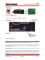
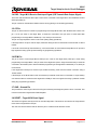
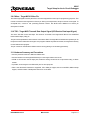
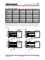
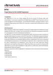
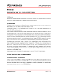
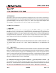
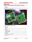
APPLICATION NOTE
M16C
Target Setup for the In-Circuit Debugger
1.0 Abstract
The ICD (In-Circuit Debugger), or USB-Monitor, is a low cost, compact interface that has two functions for
Renesas’ M16C Flash microcontrollers: 1) an in-circuit debugger tool with KD30 Debugger, and 2) an in-system
TM
programmer with FoUSB (Flash-over-USB ) Flash Programmer. The following article introduces, and shows
examples of, how to configure the target hardware with Renesas’ M16C Flash MCU to interface with the ICD for
in-circuit debugging.
2.0 Introduction
When used with KD30, the ICD provides an easy-to-use in-circuit debugging environment during application
development. In addition, when used with the FoUSB Flash Programmer, it also provides an in-system
programming interface to the target Renesas M16C Flash MCU.
The ICD, by taking advantage of Universal Serial Bus (USB), provides plug-and-play connectivity and fast data
transfers between the computer and the M16C target board. The ICD is powered by Renesas’ M37641 full speed
USB Flash MCU, which also makes it upgradeable to support future Renesas M16C MCUs.
Powering the ICD is user selectable: USB Bus powered or Target powered. When used in bus-powered mode,
the USB bus supplies power to the ICD and target board. When in target-powered mode, USB bus power is
disconnected and the ICD sources power from the M16C target board. Renesas recommends to use Target
Power Mode and NOT USB Bus Power Mode when connected to non-Renesas SKP target boards. If you plan to
use the ICD to supply power to non-SKP boards, please contact Renesas representative for details and
assistance.
Aside from a standalone kit (RTA-FoUSB-MON), the ICD comes included with the following Renesas Starter
Kits:
• MSV30102-SKP
• MSV30262-SKP
• MSV30245-SKP
• M16C System Evaluation Kit
• SKP16C26
• SKP16C28
• SKP16C62P
• SKP8CMini
REU05B0060-0101Z
March 2004
Page 1 of 8
M16C
Target Setup for the In-Circuit Debugger
PC with Windows™ 98,
2000, Me, or XP and
available USB port
Figure 1 ICD System Connectivity
A picture of the ICD with key components indicated is shown below.
10-pin Polarized
Connector to M16C
2
Target Board
Target or (USB) Bus
1
Powered Switch
Mini-USB
2
Connector
LED’s:
Red – Target Stopped
Green – Target Running
Yellow – USB-Monitor Status
Red – Power
Figure 2 ICD (or USB-Monitor)
Note:
1. The USB Bus Power Mode was designed to supply power to Renesas SKP boards.
If non-Renesas SKP boards (i.e. customer developed M16C board) are used as target boards, use the ICD in Target
Power mode. Contact your Renesas representative if you plan to use the ICD in Bus Power mode to supply power to
your non-SKP target board.
2. The ICD ships with a 6’ mini USB cable to connect to your PC and a 6” 10-pin flat ribbon target cable to connect to
the M16C target board.
3. The ICD requires 5V for re-programming if a new MCU file (MMI) needs to be downloaded to the ICD (i.e. when the
target MCU selected does not match the MCU file on the ICD). To accomplish this, disconnect the ICD from the target,
set to Bus Power Mode, and then download new MCU file. After MCU file has been downloaded, switch back to Target
Power Mode.
REU05B0060-0101Z
March 2004
Page 2 of 7
M16C
Target Setup for the In-Circuit Debugger
3.0 Target Hardware Connectivity for In-Circuit Debugging
This section describes the hardware connections to the ICD for in-circuit debugging operations. Examples for
different M16C MCU’s are shown at the end of the section. For target MCU resources used during in-circuit
debugging, see reference section for details.
The ICD connects to an M16C target board through a polarized, .100” (2.54mm), 10-pin connection using a flat
ribbon cable. It communicates with the M16C MCU using the boot UART/SIO in a clocked SIO configuration. The
signals used and how these signals are assigned is described below.
TXD
10
9
CNVss
RESET
8
7
GND
EPM
6
5
CE
RXD
4
3
SCLK
BUSY
2
1
Vcc
Figure 3 Target Board 10-Pin Header/Connector Signal Assignment
Note: All target interface lines are in high impedance state until instructed to do otherwise by the KD30 Debugger
application.
3.1 Vcc – Power Supply Pin
This provides the common connection point for power between ICD and the target board. This must be
connected to the target board’s Vcc line/plane.
In Target Power mode, the ICD requires at least 3.3V and 45mA to operate properly. The ICD requires 5V when
downloading new MCU Monitor Image (MMI).
3.2 Busy – Target MCU SIO Busy Signal
This line indicates whether the target is busy (and cannot receive data) or not. This must be connected to the
target MCU’s boot UART/SIO BUSY (CTS/RTS) pin.
This pin cannot be used while the ROM monitor is running (during in-circuit debug operations).
3.3 SCLK – Target MCU Serial Clock Signal
This clock is used for synchronous serial communication between ICD and target board. This must be connected
to the target MCU’s boot UART/SIO SCLK pin.
This pin cannot be used while the ROM monitor is running (during in-circuit debug operations).
REU05B0060-0101Z
March 2004
Page 3 of 7
M16C
Target Setup for the In-Circuit Debugger
3.4 RXD –Target MCU Receive Data Input Signal (ICD Transmit Data Output Signal)
This is the ICD SIO transmit data output. This must be connected to the target MCU’s boot UART/SIO receive
data input (RXD) pin.
This pin cannot be used while the ROM monitor is running (during in-circuit debug operations).
3.5 CE Pin
This pin is used to enter boot mode for programming of the target M16C MCU. Not all M16C MCU’s have a CE
pin. If a CE pin exists on the target MCU, it should be connected to this pin (refer to serial mode flash
programming in the target MCU’s datasheet). If not, leave pin unconnected.
This pin is in high impedance when in user mode (during debug operations).
If the target MCU’s CE pin is used as input, isolate the driving circuit from the header connection with a 1Kohm
resistor.
If to be left unconnected (if users decides to), care must be taken to ensure that the target MCU’s CE pin has a
high signal level using a pull-up resistor during any programming operations.
3.6 EPM Pin
The pin is used to control target MCU’s EPM pin (if it exists on the target MCU). EPM pin is used during
programming of the target MCU. If this pin exists on the target MCU (and in Target Powered mode), it should be
connected to the header (refer to serial mode flash programming of the target MCU’s datasheet). If not, leave pin
unconnected.
If the target MCU’s EPM pin is used as input, isolate the driving circuit from the header connection using a
1Kohm resistor.
If the EPM pin of the M16C MCU is left unconnected (no external circuit and not connected to 10-pin header),
care must be taken to ensure that the target MCU’s EPM pin has a low signal level using a pull-down resistor
during any programming operations.
3.7 GND – Ground Pin
This provides the common point where the ICD ground and target board ground planes can be connected. This
must be connected to target board’s GND line/plane.
3.8 RESET – Target MCU Reset Signal
This active low signal is used by the ICD to reset the target MCU. This must be connected to the target board’s
reset circuit or target MCU’s reset pin.
The user must ensure that the ICD can drive the pin to a valid low level with 5mA current.
REU05B0060-0101Z
March 2004
Page 4 of 7
M16C
Target Setup for the In-Circuit Debugger
3.9 CNVss – Target MCU CNVss Pin
This active high signal is used by the ICD to control the target MCU’s CNVss pin for programming purposes. This
must be connected to the target MCU’s CNVss pin. During normal operation, this pin must have a low signal. To
accomplish this, connect a 10K (nominal) pull-down resistor. See M16C MCU datasheet on CNVss pin
description for details.
3.10 TXD – Target MCU Transmit Data Output Signal (ICD Receive Data Input Signal)
This is the ICD SIO receive data input. This must be connected to the target M16C MCU’s boot UART/SIO
transmit data output (TXD) pin.
This pin must be pulled down with a resistor connected to GND. The target MCU’s ROM monitor polls this pin for
the presence of the ICD before running the user program. Without the pull-down resistor, the target MCU will only
run the ROM monitor program.
This pin cannot be used while the ROM monitor is running (during in-circuit debug operations).
3.11 Hardware Summary and Precautions
• Connect pull-down resistors to RXD and CNVss lines.
• Connect Reset line to the target MCU Reset pin or the target board’s reset circuit.
• If EPM or CE lines are used as input pins, isolate the driving circuit from the 10-pin header using a 1Kohm
resistor.
• If possible, avoid using the boot SIO/UART pins for other purposes.
• Table 1 lists the M16C Flash MCU’s supported, CE or EPM pin support, the boot UART/SIO, DBC interrupt
support, and the number of breakpoints that can be set in KD30.
REU05B0060-0101Z
March 2004
Page 5 of 7
M16C
Target Setup for the In-Circuit Debugger
Table 1 M16C MCU Support Summary
M16C MCU
CE/EPM Pin
Boot UART/SIO
DBC Irq Support
Breakpoints
M16C/10
None
UART0
No
2
M30245FC
Both
UART1
No
2
M16C/26
CE
UART1
Yes
6
M16C/28
CE
UART1
Yes
6
M16C/29
CE
UART1
Yes
6
M3062GF8N
Both
UART1
No
2
M16C/62P, 6N
Both
UART1
Yes
8
M306V7FG
Both
UART0
No
2
R8C/10, /11
None
UART1
Yes
2
Examples of target board hardware connection to 10-pin header (ICD) when used for debugging purposes only.
If you cannot find your M16C Flash MCU in the examples shown, please contact Renesas representative for
assistance.
10-Pin
Header
Vcc
BUSY
CLK
RxD
CE
EPM
GND
!RESET
CNVss
TxD
Vcc
P6_4/RTS1 (Busy)
P6_5/CLK1 (SCLK)
P6_6/RxD1 (RxD)
P8_6/XCout (CE)
1
2
3
4
5
6
7
8
9
10
Vss
!RESET
CNVss
P6_7/TxD1 (TxD)
47K
(nominal)
REU05B0060-0101Z
10-Pin
Header
Vcc
P6_4/RTS1 (Busy)
P6_5/CLK1 (SCLK)
P6_6/RxD1 (RxD)
P5_0/WRL (CE)
P5_5/HOLD (EPM)
Vss
!RESET
CNVss
P6_7/TxD1 (TxD)
1
2
3
4
5
6
7
8
9
10
47K
(nominal)
Vcc
P1_7/CNTR0 (Busy)
P1_6/CLK0 (SCLK)
P1_5/RxD0 (RxD)
1
2
3
4
5
6
7
8
9
10
Vss
!RESET
CNVss
P1_4/TxD0 (TxD)
47K
(nominal)
M30245F
Vcc
M16C/10
Vcc
Vcc
BUSY
CLK
RxD
CE
EPM
GND
!RESET
CNVss
TxD
47K
(nominal)
10-Pin
Header
Vcc
BUSY
CLK
RxD
CE
EPM
GND
!RESET
CNVss
TxD
10-Pin
Header
M16C/26, M16C/28,
M16C/29
Vcc
Vcc
BUSY
CLK
RxD
CE**
EPM
GND
!RESET
CNVss
TxD
47K
(nominal)
Vcc
47K
(nominal)
R8C/10, R8C/11
Vcc*
MODE (Busy)
CNVss (SCLK)
P3_7 (RxD1)
1
2
3
4
5
6
7
8
9
10
Vss
!RESET
P0_0 (TxD1)
47K
(nominal)
March 2004
47K
(nominal)
47K
(nominal)
Page 6 of 7
M16C
Target Setup for the In-Circuit Debugger
Vcc
10-Pin
Header
Vcc
BUSY
CLK
RxD
CE*
EPM*
GND
!RESET
CNVss
TxD
10-Pin
Header
M16C/62P
Vcc
Vcc1
P6_4/RTS1 (Busy)
P6_5/CLK1 (SCLK)
P6_6/RxD1 (RxD)
P5_0/WRL (CE)
P5_5/HOLD (EPM)
Vss
!RESET
CNVss
P6_7/TxD1 (TxD)
1
2
3
4
5
6
7
8
9
10
47K
(nominal)
Vcc
BUSY
CLK
RxD
CE*
EPM**
GND
!RESET
CNVss
TxD
RHOLD***
47K (nominal)
Vcc1
P6_4/RTS1 (Busy)
P6_5/CLK1 (SCLK)
P6_6/RxD1 (RxD)
P5_0/WRL (CE)
P5_5/HOLD (EPM)
Vss
!RESET
CNVss
P6_7/TxD1 (TxD)
1
2
3
4
5
6
7
8
9
10
47K
(nominal)
47K
(nominal)
* CE and EPM pins are high impedance in user mode (during debug).
M16C/62P in
Expanded Memory
Mode
47K
(nominal)
* CE and EPM pin are high impedance in user mode (during debug ).
** HOLD/EPM pin must be pulled high in memory expansion mode.
Note: If you cannot find your M16C Flash MCU in the examples shown, please contact Renesas representative for
assistance.
4.0 Conclusion
The ICD is an easy-to-use interface for setting up an M16C MCU development environment to support in-circuit
debugging. It does not require a lot of resources from the target board. Correct hardware connectivity will
guarantee proper operation.
5.0 Reference
Renesas Technology Corporation Semiconductor Home Page
http://www.renesas.com
E-mail Support
[email protected]
User’s Manual
• RTA-FoUSB-MON User’s Manual
• Target Setup for FoUSB Programmer App Note
• Firmware Requirements for In-Circuit Debugger Support App Note
REU05B0060-0101Z
March 2004
Page 7 of 7
Keep safety first in your circuit designs!
• Renesas Technology Corporation puts the maximum effort into making semiconductor products
better and more reliable, but there is always the possibility that trouble may occur with them. Trouble
with semiconductors may lead to personal injury, fire or property damage.
Remember to give due consideration to safety when making your circuit designs, with appropriate
measures such as (i) placement of substitutive, auxiliary circuits, (ii) use of nonflammable material or
(iii) prevention against any malfunction or mishap.
Notes regarding these materials
• These materials are intended as a reference to assist our customers in the selection of the Renesas
•
•
•
•
•
•
•
Technology Corporation product best suited to the customer's application; they do not convey any
license under any intellectual property rights, or any other rights, belonging to Renesas Technology
Corporation or a third party.
Renesas Technology Corporation assumes no responsibility for any damage, or infringement of any
third-party's rights, originating in the use of any product data, diagrams, charts, programs, algorithms,
or circuit application examples contained in these materials.
All information contained in these materials, including product data, diagrams, charts, programs and
algorithms represents information on products at the time of publication of these materials, and are
subject to change by Renesas Technology Corporation without notice due to product improvements
or other reasons. It is therefore recommended that customers contact Renesas Technology
Corporation or an authorized Renesas Technology Corporation product distributor for the latest
product information before purchasing a product listed herein.
The information described here may contain technical inaccuracies or typographical errors.
Renesas Technology Corporation assumes no responsibility for any damage, liability, or other loss
rising from these inaccuracies or errors.
Please also pay attention to information published by Renesas Technology Corporation by various
means, including the Renesas Technology Corporation Semiconductor home page
(http://www.renesas.com).
When using any or all of the information contained in these materials, including product data,
diagrams, charts, programs, and algorithms, please be sure to evaluate all information as a total
system before making a final decision on the applicability of the information and products. Renesas
Technology Corporation assumes no responsibility for any damage, liability or other loss resulting
from the information contained herein.
Renesas Technology Corporation semiconductors are not designed or manufactured for use in a
device or system that is used under circumstances in which human life is potentially at stake. Please
contact Renesas Technology Corporation or an authorized Renesas Technology Corporation product
distributor when considering the use of a product contained herein for any specific purposes, such as
apparatus or systems for transportation, vehicular, medical, aerospace, nuclear, or undersea
repeater use.
The prior written approval of Renesas Technology Corporation is necessary to reprint or reproduce in
whole or in part these materials.
If these products or technologies are subject to the Japanese export control restrictions, they must be
exported under a license from the Japanese government and cannot be imported into a country other
than the approved destination.
Any diversion or reexport contrary to the export control laws and regulations of Japan and/or the
country of destination is prohibited.
Please contact Renesas Technology Corporation for further details on these materials or the
products contained therein.