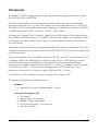
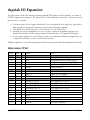
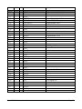
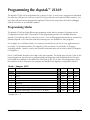
1
Danville Signal Processing, Inc.
dspstak™ 21369 Family
User Manual
Version 1.00
Danville Signal Processing, Inc.
dspstak™ 21369 Family User Manual
Copyright © 2006 Danville Signal Processing, Inc. All rights reserved. Printed in the USA.
Under the copyright laws, this manual may not be reproduced in any form without prior written
permission from Danville Signal Processing, Inc.
Danville Signal Processing, Inc. strives to deliver the best product to our customers. As part of this
goal, we are constantly trying to improve our products. Danville Signal Processing, Inc., therefore,
reserves the right to make changes to product specification or documentation without prior notice.
Updated operating manuals and product specification sheets are available at our website for
downloading.
This manual may contain errors, omissions or “typo’s”. Please send your comments, suggestions and
corrections to:
Danville Signal Processing, Inc.
38570 100th Avenue
Cannon Falls, MN 55009-5534
Trademark Notice
dspstak and dspblok are trademarks of Danville Signal Processing, Inc. VisualDSP++, EZ-Kit,
VisualAudio and SHARC are trademarks of Analog Devices, Inc. CyberClocks is a trademark of
Cypress Semiconductor Corporation. Windows is a trademark of Microsoft Corporation.
Contact Information
Danville Signal Processing, Inc.
38570 100th Avenue
Cannon Falls, MN 55009
E-mail:
Web Site:
[email protected]
http://www.danvillesignal.com
Voice:
Fax:
507-263-5854
877-230-5629
dspstak™ 21369 User Manual
Page 2
Table of Contents
Overview ..........................................................................5
Introducing dspstak™.............................................................................5
dspstak™ 21369 ....................................................................................5
Introduction...........................................................................................7
Hardware Description......................................................9
dspblok 21369zx ...................................................................................9
Power Supply ........................................................................................9
RS-232 Interface ..................................................................................10
USB Interface (zx versions only) ...........................................................11
USB Interface (zx2 versions only) .........................................................11
Interconnect Port .................................................................................12
Programmable Clocks ..........................................................................12
JTAG Emulation Port ............................................................................12
EZ-Kit Style Debugger (ICE versions only) .............................................13
dspstak™ 21369 Architecture ........................................14
System Description ..............................................................................14
DAI......................................................................................................15
DPI ......................................................................................................15
External Port ........................................................................................16
I/O Register & DPI Expansion...............................................................16
I/O Register Map..................................................................................17
I/O Register Commands .......................................................................17
Programming the Clock........................................................................19
dspstak I/O Expansion....................................................21
Interconnect Port .................................................................................21
Development Tools ........................................................23
dspstak™ 21369 User Manual
Page 3
Visual DSP++ 4.5 for SHARC .............................................................23
VisualAudio .........................................................................................24
EZ-KIT style Debugger (with ICE versions) ............................................24
Installing Visual DSP++ 4.5 (Kit License, with ICE versions) .................24
Installing the debugger in Visual DSP++ 4.5 (ICE versions) ..................25
Power-up Procedure............................................................................25
Programming the dspstak™ 21369 ................................26
Programming Modes............................................................................26
Boot & Clock Configuration .................................................................27
Uploading Programs – Modes 6 & 7.....................................................27
Uploading Procedure...........................................................................28
Software..........................................................................30
Schematic .......................................................................30
Mechanical Drawings.....................................................30
Product Warranty ...........................................................31
RoHS & WEEE Compliance.............................................32
dspstak™ 21369 User Manual
Page 4
Overview
DSP-based embedded applications often take the form of a digital signal processing engine coupled
with a specialized data conversion and signal conditioning front end. The front end electronics and
the DSP are almost always connected via high speed serial ports and the general purpose I/O ports
of the DSP. In most cases, once the local memory and peripheral interfacing needs of the DSP are
fulfilled, the DSP’s data and address busses are no longer needed.
Standardized bus architectures such as PC/104, PCI and cPCI are all based on communicating via
each board’s data and address bus, while ignoring the needs of the most DSP / data conversion
interfaces.
Introducing dspstak™
Danville’s dspstak modules are designed to simplify DSP-based embedded applications. Generally,
each dspstak consists of two or more modules: a DSP Engine, and a signal conditioning/data
conversion I/O Module(s). The Interconnect Port consists of SPORTs (high speed serial ports), SPI,
general I/O, clocks and power connections.
DSP Engine modules generally consist of a DSP processor, memory, power supplies and standard
digital I/O such as RS-232 and USB. We currently have products based on Analog Devices’ SHARC®
processors.
The I/O Modules may include signal conditioning electronics, A/D and/or D/A data converters,
audio transceivers, unique connectors and a plethora of other special front end requirements. Since
the I/O Module is separate from the DSP Engine Module, custom interfaces can be created quickly
and inexpensively. Danville has a number of standard I/O Modules and often is willing to create a
new one based on customer request. You can also create your own.
dspstak™ 21369
This manual covers the dspstak 21369 family of DSP Engines and is complemented by the dspstak
Family Users Manual. The family manual covers topics that all dspstaks have in common. You will
want to review the family manual for mechanical dimensions, system configurations, basic
connector specifications, etc.
The dspstak 21369 manual covers topics that are relevant to the specific implementation of dspstak
21369 DSP Engines. Currently, there are four members of this family.
•
•
dspstak 21369zx
dspstak 21369zx with ICE
dspstak™ 21369 User Manual
Page 5
•
•
dspstak 21369zx2
dspstak 21369zx2 with ICE
Most of the features of these products are identical. When we are describing these common
features, the product will be referred to as dspstak 21369.
The products vary in two ways: the choice of USB interfaces and whether a built in EZ-KIT style
debugger (ICE) is included.
The dspstak 21369zx and dspstak 21369zx with ICE include a USB interface based on an FTDI
FT245RL. This USB interface is very easy to use and has support for most popular operating systems.
In general, it looks like a very fast COM port to the computer. In many cases, a terminal program is
all that is needed to use this interface. The main limitation of this interface is that it is restricted to
full speed (12Mb/s) and therefore limited in the amount of data that can be transferred. We suggest
using this version when the USB acts primarily as a control port.
The dspstak 21369zx2 and dspstak 21369zx2 with ICE include a USB interface based on a PLX
NET2272. This device is capable of high-speed transfers (480Mb/s). It is very similar to the USB
interface used in Analog Devices’ SHARC USB EZ-Extender. There is USB driver support for
Windows XP and 2K included in Visual DSP++ 4.5. These include a high-speed bulk driver and
an audio class driver. In general, you would use these drivers as part of a software application
written for Windows. The audio driver works like a sound card.
The “with ICE” versions are used during the development process. They have exactly the same
footprint as the production versions. This allows you to develop your product without an external
emulator and then substitute lower cost boards when your product is ready for production. The
“with ICE” boards are supported by Visual DSP++. You can use a free KIT license (same restrictions
as an EZ-KIT) or the full-featured version. Danville also has platform files for Analog Devices’
VisualAudio graphical development tool. Most of our dspstak 21369 – dspstak I/O module
combinations are supported.
All dspstak 21369 boards have JTAG connections to accommodate an ADI HPUSB or USB ICE. If
you have one of these emulators, then any version of the dspstak 21369 can be used for
development.
Intended Audience
The dspstak 21369 is intended for DSP systems integrators, designers and programmers who may
wish to integrate a dspstak into their products. This manual is primarily aimed at users who have a
working knowledge of microcomputer technology and DSP related design. We assume that you are
familiar with the Analog Devices ADSP-21369 SHARC DSP.
dspstak™ 21369 User Manual
Page 6
Introduction
The dspstak™ 21369 is a high performance digital signal processing engine based on the Analog
Devices ADSP-21369 SHARC DSP.
The ADSP-21369 supports 32 bit fixed point and 32/40 bit floating point formats with SIMD
instructions running at up to 333 MHz. This translates to a peak computation rate of 2.0 GFLOPS.
The ADSP-21369 has very flexible peripherals including up to 8 independent serial ports (SPORTs),
8 sample rate converters (SRCs), 2 SPI ports, TWI (I2C), and 2 UARTs.
The heart of the dspstak 21369 is Danville’s dspblok 21369zx DSP Module. This module includes
flash, SDRAM and EEProm memory. The dspblok 21369zx is also available as a standalone module
for integration into other boards. You may wish to review the dspblok 21369zx User Manual for
more information.
The dspstak 21369 Interconnect Port supports the complete DAI interface, SPI, general I/O, clocks
and power connections. The dspstak 21369 also includes USB and RS-232 ports for easy interfacing
to the outside world.
Program development is very easy with the dspstak 21369. The “with ICE” versions includes a builtin emulator similar to the debugger that is built into Analog Devices’ EZ-Kit family of evaluation
boards. This technology was provided by Analog Devices and is licensed to Danville Signal
Processing. The emulator is supported by Visual DSP++ (Version 4.5 and later). Since it looks like
an EZ-Kit to Visual DSP++, you may use the debugger with an EZ-Kit license (free, with
performance restrictions) or you may use it with a Full Visual DSP++ license.
A JTAG interface is also available to connect an Analog Devices external ICE.
The dspstak 21369 includes the following items:
Hardware:
•
dspstak 21369 board (including dspblok 21369zx)
Documents & Programs (CD):
•
•
•
•
•
This Manual
dspstak Family User Manual
dspblok 21369zx User Manual
Free Terminal Program – Tera Term Pro
USB Device Driver
dspstak™ 21369 User Manual
Page 7
Firmware (CD):
•
•
Sample Programs
VisualAudio platform files
Development Tools (ICE Versions Only):
•
•
•
Analog Devices’ Visual DSP ++ 4.5 – KIT Version
Visual DSP++ Installation file
Cables
Schematics (CD):
•
•
dspblok 21369zx
dspstak 21369
We recommend that you have the following tools and documents:
•
•
•
•
•
•
Analog Devices VisualDSP++™ for SHARC® (Version 4.5 or later)
Analog Devices ADSP-21368 SHARC Hardware Reference Manual
Analog Devices ADSP-2136x SHARC Processor Programming Reference Manual
Analog Devices ADSP-21160 SHARC Instruction Set Reference Manual
Analog Devices ADSP-21369 Product Data Sheet
Cypress Semiconductor CyberClocks™
You may also want the following tools and documents for more advanced development:
•
•
Analog Devices HP ICE
Danville JTAG Adapter (required for ADI ICE)
Danville is an authorized reseller of ADI tools including Visual DSP++ and the emulators. If you
need one of these tools, we would appreciate your business.
Our website (www.danvillesignal.com) has downloads and links to other supplementary tools and
documents.
dspstak™ 21369 User Manual
Page 8
Hardware Description
The dspstak 21369 includes all dspstak DSP Engine standard features. These features are discussed
in a general way in the dspstak Family Users Manual and are as follows:
•
•
•
•
•
•
Power Supply
RS-232 Interface
USB Interface
Interconnect Port
Programmable Clock
JTAG Ports
Each of these areas is discussed in more detail in this manual.
Even though this manual addresses the dspstak 21369 specifically, there are several related products
that may be important to you. The third generation SHARC family includes several pin compatible
parts. These DSPs may have special licensed algorithms programmed into their ROM (ADSP-21367
for example) or enhanced peripherals (ADSP-21368 for example). Danville offers dspstak products
that support these processors. Since the core of the dspstak 21369 platform is a dspblok module,
exchanging dspblok modules is an easy way to support different DSPs and core functions. You can
also use the dspblok as a component in your own target. In this case, the dspstak baseboard is a
useful test platform.
dspblok 21369zx
The heart of the dspstak 21369 is a dspblok 21369zx. This module includes the ADSP-21369 DSP,
flash memory, EEProm and SDRAM. You can use a dspblok 21369zx as an independent building
block module and you can use it as the DSP Engine component in a dspblok system. Details of the
dspblok 21369zx are covered in the dspblok 21369zx User Manual.
Power Supply
The dspstak 21369 uses a standard 2.1/5.5mm coaxial power jack to provide power to itself and
also any I/O modules via the Interconnect Port. From the dspstak 21369 view, this supply may be
either an AC supply or a DC supply with the center of the coaxial power plug connected as the
positive pin. Adjacent to the coaxial jack, there are 3 pads spaced at 0.100 inch that may be used
as an alternative connection to provide a bipolar DC supply to the board. These pads are labeled
JH7 and can accommodate a .025 header or similar connector.
dspstak™ 21369 User Manual
Page 9
The incoming voltage is half wave rectified to create new unregulated DC supplies called Va+ and
Va-. From these unregulated supplies, Va+5 (5.0 Volt Analog) and Vd+5 (5.0 Volt Digital) are
created and made available to the I/O Modules via the Interconnect Port. Vd+5 is the same as
Va+5 with a different ground return. It is included for compatibility with older dspstak DSP
Engines. An additional internal supply is also created to provide the input to switching regulators
that are used for digital supplies. The main dspstak digital supply is Vd+3.3 (3.3V). The dspblok
21369 includes a switching supply for its core power supply requirement.
The dspstak 21369 DSP Engine does not use Va+, Va-, Va+5 or Vd+5. These supplies are
available to I/O Modules. If the I/O Module does not need a negative supply, you can power the
dspstak 21369 with only a positive DC power supply. The recommended input voltages are 9 VAC
or 9 to 15VDC. Since switching regulators are used for the digital supplies, the input voltage is not
critical.
In all cases, the DC supply or an unregulated DC supply created from an incoming AC supply
should be less than 20VDC. This will protect both the DSP Engine and probably the components on
the I/O Module.
One final thing to remember: The nominal output voltage of a wall adapter is usually much lower
than its actual output voltage. We recommend that unregulated DC wall adapters should have a
maximum nominal voltage of 12VDC.
RS-232 Interface
The RS-232 interface is used to upload user application programs for the DSP. An application
program may also use the RS-232 interface for its own purposes.
The RS-232 interface is configured as a DCE (Data Communications Equipment) device. It uses a
DB-9F connector that is designed to mate without crossover connections to the DB-9M connector
found on PC compatible computers. Connections are defined in the following table:
Signal
DCD
RD
TD
DTR
SIGNAL GND
DSR
RTS
CTS
RI
Direction
DCE -> DTE
DTE -> DCE
DTE -> DCE
DCE -> DTE
dspstak™ 21369 User Manual
Pin
1
2
3
4
5
6
7
8
9
Notes
DCD, DTR & DSR are connected together
DCD, DTR & DSR are connected together
DCD, DTR & DSR are connected together
dspstak I/O Register 0
dspstak I/O Register 0
NC
Page 10
When the dspstak 21369 is programmed using the RS-232 interface, only RD & TD are used. DTR,
DSR & DCD are simply connected together and ignored by the dspstak. Since the RS-232 port is
used in a very standardized manner, a USB to RS-232 converter can be used with computers that
no longer support RS-232 serial communications.
USB Interface (zx versions only)
The zx USB interface is another way that programs may be uploaded to the dspstak. This interface
should not be confused with the debugger (on board ICE), which uses its own mini-B USB
connector. The USB interface is also available for user applications. A device driver is included with
the dspstak 21369 to support Windows 2000 & Windows XP applications. The USB connection is
made via a standard USB type B connector.
The USB port on the dspstak 21369zx uses an FTDI FT245RL USB transceiver. This device is a USB
2.0 compliant, full speed part (12Mb/s). This part is very easy to use since in most cases it just looks
like a COM Port to the USB Master. FTDI has royalty free device drivers on their web site that
support a variety of operating systems. We suggest that you visit their web site (www.ftdichip.com)
for additional information.
We supply Windows® drivers on our distribution CD. The driver files includes dspstak *.inf files
that are used for installation in Microsoft Windows® operating systems. If you are using another OS,
you may want to compare the ftdibus.inf and ftdiport.inf files to the dspstakbus.inf and
dspstakport.inf files to configure your driver. Instructions on installing the Windows® drivers are on
the CD.
The zx USB registers are mapped into the dspstak I/O register space. There is an example of how to
read and write the USB included in the sample software on the CD.
USB Interface (zx2 versions only)
The zx2 USB uses a PLX NET2272 USB transceiver. This device is a USB 2.0 compliant, high-speed
part (480Mb/s). It is supported with two Windows device drivers supplied with Visual DSP++ 4.5
as part of the 213xx examples (../Visual DSP 4.5/213xx/Examples/USB EZ-Extender). The circuit
implementation is functionally identical with the exception of the line used for reset.
The distribution CD includes a dspstak 21369 implementation of the ADI examples.
Presently, The zx2 USB port cannot upload code to the dspstak 21369 flash. This function is
handled exclusively by the RS-232 port.
dspstak™ 21369 User Manual
Page 11
The USB connection is made via a standard USB type B connector. This interface should not be
confused with the debugger (on board ICE), which uses its own mini-B USB connector.
Interconnect Port
The Interconnect Port is the only standard connection between the DSP Engine and I/O Modules.
This port is described in detail in the dspstak Family Users Manual and the dspstak I/O Expansion
section of this manual.
Programmable Clocks
The dspstak 21369 has a very flexible clock configuration. A user reprogrammable clock generator
provides the DSP clock and three I/O clocks that are available on the Interconnect Port. The three
programmable clocks on the Interconnect Port allow I/O Modules to use convenient clocks for
whatever devices that might be present. For example, an ADC might use an 18.432 MHz MCLK to
sample at 96k or a 19.6608 MHz MCLK to sample at 102.4k. In addition to the on-board
programmable clock, the DSP clock can also be provided externally by a dspstak I/O Module.
The dspstak 21369 uses a Cypress Semiconductor CY22393 flash programmable clock generator.
This device has three PLLs which when combined with the reference oscillator can create four
independent clock frequencies. Cypress has a program called CyberClocks on their web site
(www.cypress.com) that you can use to create a JEDEC file to reprogram the clock chip. There are
two standard clock configurations that are available by selecting the Clock Select Bit in the dspstak
I/O register. The CY22393 is also reconfigurable by directly writing its registers via TWI (I2C). There
are supporting library functions in the code examples.
In many cases, the factory default settings are appropriate and no changes are ever necessary.
JTAG Emulation Port
The dspstak 21369 has a right angle 2mm connector mounted on the dspblok assembly. This
connector is accessible even when a dspstak I/O Module is positioned above the dspstak 21369.
The JTAG connector is smaller than the standard ADI JTAG header. The Danville JTAG connector is
a male 16 pin, 2mm dual row header. A JTAG adapter is available from Danville to convert the
2mm header to the 0.100 headers used by the Analog Devices emulators.
If you are using an external ICE for the DSP, the built-in debugger is automatically disconnected.
When you are not using an ICE or ByteBlaster, leave the JTAG pins open.
dspstak™ 21369 User Manual
Page 12
EZ-Kit Style Debugger (ICE versions only)
The dspstak 21369 debugger uses a mini-b USB connector (J5). The technology is provided under
license from Analog Devices for use with the dspstak 21369. It is not Danville’s property and
therefore we will not discuss specifics or disclose circuit information. Here are the important facts:
•
•
•
•
•
It is supported by Visual DSP++ (Version 4.5 or later).
It looks like an EZ-Kit to Visual DSP++. You can use the EZ-Kit license with the feature
restrictions or you can use a full Visual DSP++ license.
We include an installation CD of Visual DSP++ 4.5 with a KIT license. You should install
any updates that are on the Analog Devices website and register the product with ADI.
It only supports the ADSP-21369 on the dspstak.
Contact Danville if you want to use a different DSP processor.
dspstak™ 21369 User Manual
Page 13
dspstak™ 21369 Architecture
System Description
The dspstak 21369 platform is intended for embedded signal processing applications where the
benefits of a 32 bit fixed and floating point DSP are apparent. The dspstak architecture is tailored to
take advantage of the third generation SHARC DSP family. These issues are discussed in more detail
in our dspstak Family User Manual (Version 2.00).
The block diagram above illustrates the basic dspstak 21369 architecture with all the variations on
the same drawing. The ADSP-21369 has a rich set of peripherals, which are extended by the
addition of a USB transceiver and a programmable clock generator. The core functions are
provided by a dspblok 21369zx, which includes the DSP, flash, EEProm and SDRAM.
I/O is connected to the dspstak 21369 via the Interconnect Port. This is a 96 pin DIN connector
that is described in detail in its own section in this manual.
dspstak™ 21369 User Manual
Page 14
A major requirement for a general-purpose solution such as the dspstak 21369 is that resources
cannot be squandered. It is very important that the dspstak core maintain maximum flexibility since
the exact user application is not known ahead of time. The logical starting place to consider is the
DSP since all the other components are “supporting cast”.
The DSP has the following external interfaces:
•
•
•
Digital Audio Interface (DAI)
Digital Peripheral Interface (DPI)
External Port
DAI
The DAI is comprised of a group of peripherals including the SPORTs and a signal routing unit.
There are 20 pins on the DSP that connect the DAI to the outside world. All 20 DAI pins are
available on the Interconnect Port. It is the DAI that really enables a dspstak to work with a large
number of different I/O requirements.
Most digital signal (and general purpose) processors have a finite number of peripherals that are
individually mapped to specific pins on the device. If you want to support a large number of
options, you need a large number of pins. Since larger pin counts usually means higher cost, there is
a tendency to have fewer features. Of course, most applications don’t need all the possible features,
but the set they do need is seldom universal.
The third generation SHARC solves this problem by providing a large number of peripherals behind
a 20 pin crossbar switch (the DAI). In the ADSP-21369, there are 8 SPORTS, 8 sample rate
converters (SRCs), an S/PDIF transceiver, 4 precision clock generators (PCGs) and a high-speed
parallel input FIFO. The DAI pins can also function as general purpose I/O. The DAI allows you to
select the ones you want in an “a la Carte” fashion.
The dspstak 21369 does not use any of the DAI pins for internal functions, therefore all DAI pins
are available for dspstak I/O.
DPI
The DPI expands on the DAI concept by abstracting the general-purpose microcontroller
peripherals to 14 assignable pins on the DSP. Earlier third generation SHARCs like the ADSP-21262
have fewer peripherals so dedicated pins were used or in some cases shared with the DAI.
dspstak™ 21369 User Manual
Page 15
The DPI provides 2 SPI ports, 2 UARTs, a TWI (I2C) port, and general purpose I/O. The dspstak
21369 takes advantage of many of these built-in peripherals so unlike the DAI, many of the DPI
pins are not externally available.
Most modern data converters and many other devices rely on SPI communications for control and
configuration. The dspstak places a strong emphasis on SPI based communications, therefore
additional hardware support has been added to expand SPI capabilities via the Interconnect Port.
There are two SPI ports on the ADSP-21369. The dspstak 21369 uses SPI 0 as its primary SPI
interface. The DSP is always the master and uses this interface to boot from flash, read/write
external memory, configure I/O, etc. The remaining SPI port is unused and could be configured as a
slave for an external processor interface.
The TWI (I2C) interface is used internally to control the programmable clocks. It could be
reassigned to external pins on the Interconnect Port. UART 0 is used for the RS-232 interface.
In addition to the SPI 0 port, there are five DPI pins that are available on the Interconnect Port.
External Port
The external port provides an asynchronous data bus and supports 32 bit wide 133 MHz SDRAM.
64Mbit (2M x 32) SDRAM is provided as part of the dspblok 21369zx. The data bus is used to
expand the local I/O of the dspstak 21369 including connections to the USB transceiver.
The external port is not expanded to off board connectors to insure that all high-speed bus
communications are successful. Applications that require access to the asynchronous data bus, may
want to consider using a dspblok 21369zx independently.
I/O Register & DPI Expansion
A PLD is used to expand I/O via the External Port using #MS2, A1 & A0. This mapping defines four
register addresses. Only the lowest byte (D7-D0) is valid, the upper bytes will read as high and
should be masked in software.
The PLD is also used to buffer the SPI port where the DSP is always configured as an SPI master.
Since dspstak I/O often uses many SPI devices, buffering extends the SPI drive capability and also
automatically controls MISO to prevent contention from external devices. With the SPI SS register,
multiple devices can be written at the same time with only one device responding if the mask is set
correctly.
A subset of the I/O Register is implemented in Danville’s dspblok ps-usb and dspblok ps-uart
products. The Mode bits are duplicated in Registers 0 & 3 to minimize logic requirements for
dspstak™ 21369 User Manual
Page 16
dspblok applications. USB RESET in Register 0 is defined as RS-485/RS-422 SELECT in the dspblok
ps-uart since it has no need to support the high-speed zx2 USB.
The following table shows the I/O Register. Depending on the version of the dspstak 21369, some
registers will not be valid since the USB port is implemented differently. You can write any value to
the upper bytes of Registers 0, 1 & 2 (Register 3 is read only). These bits do not point any
corresponding hardware, however we recommend that you write 0 to these bits for future
capability. The upper bytes will return 1’s regardless of any previous writes since the data bus has
pull-ups.
I/O Register Map
Name
Addr
D7
D6
D5
D4
D3
D2
D1
D0
System
0W
GP1
DIR
GP1
DIR
GP0
DIR
GP0
DIR
GP1
GP0
CTS
GP0
RTS
USB
RESET
MODE
1
RESET
GP1
CLK
SEL
MODE
2
SS4
IO3
SS5
IO4
SS3
IO2
SS4
IO3
SS2
IO1
SS3
IO2
SS1
IO0
SS2
IO1
SS1
IO0
0R
SPI SS
Notes:
MODE
0
1W
1W
IR
1R
0
0
0
0
SS5
IO4
0
0
SS
FTDI USB
2W
2R
D7
D7
D6
D6
D5
D5
D4
D4
D3
D3
D2
D2
D1
D1
D0
D0
MODE USB
STATUS
3R
1
MODE
2
MODE
1
MODE
0
0
USB
PD
USB
TXE
USB
RXF
1 = SPI
0 = I/O
Read Only
I/O Register Commands
This register supports a variety of internal and external functions. GP1 & GP0 are general
purpose I/O mapped to the Interconnect Port. CTS & RTS are handshaking lines used for RS232. Note that CTS is an output since the RS-232 port is defined as a DCE.
System – Register 0
GP1 DIR:
GP0 DIR:
GP1:
GP0:
D7
D6
D5
D4
R/W
R/W
R/W
R/W
GP0 Direction
1=Output, 0=Input
GP1 Direction
1=Output, 0=Input
General Purpose I/O
General Purpose I/O
CTS:
D3
W
RS-232 Output – DCE Perspective
dspstak™ 21369 User Manual
Page 17
RTS:
D3
R
RS-232 Input – DCE Perspective
CLK SEL:
D2
USB RESET: D1
RESET:
D0
W
W
W
Selects Programmable Clock Settings (CY22393 S2)
Resets High Speed USB (ignored in zx)
I/O Reset (interconnect Port)
MODE :
R
Mode 7 – Upload code at 115k
Mode 6 – Upload code at 19.2k
Mode 5, 4 – Reserved
Modes 3-0 – User Modes
D2-D0
All other bits are Don’t Care.
SPI SS – Register 1
SP1 Slave Select is used to enable the MISO buffer when using the pin as a SPI slave select. If
the bit is 0, then the pin can be used as general purpose I/O or any other DPI function. If an
SPI device is write only (no MISO required), then this setting can be ignored.
SS5:
IO4:
D5
D5
R/W
R/W
1 = Slave Select (Flag 0 must be an output)
0 = General Purpose (Flag 0)
SS4:
IO3:
D5
D5
R/W
R/W
1 = Slave Select (DPI 14 must be an output)
0 = General Purpose (DPI 14 function)
SS3:
IO2:
D5
D5
R/W
R/W
1 = Slave Select (DPI 13 must be an output)
0 = General Purpose (DPI 13 function)
SS2:
IO1:
D5
D5
R/W
R/W
1 = Slave Select (DPI 4 must be an output)
0 = General Purpose (DPI 4 function)
SS1:
IO0:
D5
D5
R/W
R/W
1 = Slave Select (DPI 8 must be an output)
0 = General Purpose (DPI 8 function)
SS:
D5
D5
R/W
R/W
1 = Slave Select (DPI 7 must be an output)
0 = General Purpose (DPI 7 function)
All other bits are Don’t Care.
dspstak™ 21369 User Manual
Page 18
USB Data (zx version) – Register 2
This is the data bus of the zx USB transceiver. You should not read or write to this register
without checking the status bits in Register 3. The zx2 versions do not use this register and
will return 0xFF.
Mode & USB Status – Register 3
The Mode is identical to the state of Mode in Register 0, The USB status bits are only valid in
the zx versions. They will read 1 in zx2 versions.
1:
MODE :
D7
D6-D4
R
R
0:
USB PD:
USB TXE:
USB_RXF:
D3
D2
D1
D0
R
R
R
R
Always a 1
Mode 7 – Upload code at 115k
Mode 6 – Upload code at 19.2k
Mode 5, 4 – Reserved
Modes 3-0 – User Modes
Always a 0
0 = zx USB enumerated
0 = zx USB transmit FIFO not full, can write a byte
0 = zx USB receive FIFO not empty, can read a byte
All other bits are Don’t Care.
Programming the Clock
The dspstak 21369 uses a Cypress Semiconductor CY22393 programmable clock generator to
provide clocks for the ADSP-21369 and the Interconnect Port. The Interconnect Port clocks are
SYSCLK, MCLK0 & MCLK1.
The CY22393 has three independent PLLs that allow you to generate clocks that are appropriate for
your situation. The CY22393 starts with a 24.576 MHz crystal based clock to derive the new
clocks. The three programmable clocks on the Interconnect Port allow I/O Modules to use
convenient clocks for whatever devices that might be present. For example, an ADC might use a
18.432 MHz MCLK to sample at 96k or a 19.6608 MHz MCLK to sample at 102.4k.
If you want to reprogram the CY22393, you should review the CY22393 data sheet. You will also
need the Cypress program, CyberClocks™ to generate a JEDEC file of clock parameters. The data
sheet and the program are available on the Cypress web site and there are links on the Danville
web site at http://www.danvillesignal.com.
There are two predefined sets of clock frequencies that are be switched by CLK SEL in I/O Register
0. The default settings are Clk Set 0.
dspstak™ 21369 User Manual
Page 19
Clock Configuration – CY22393
Clock
CY22393
Clk Set 1
Clk Set 0
(Default)
DSP Clock (JH1 Pins 2&3)
SYSCLK
MCLK0
MCLK1
Not Used
CLKC
CLKD
CLKA
CLKB
CLKE
22.1184 MHz
22.1184 MHz
22.5792 MHz
8.192 MHz
Off
22.1184 MHz
22.1184 MHz
24.576 MHz
12.288 MHz
Off
The clock choices are somewhat arbitrary. The DSP clock uses 22.1184 MHz since this ideal for
setting the UART to common bauds such as 115.2k and 38.4k. It also conveniently scales to 331.78
MHz by multiplying by 15. This is the maximum core clock supported by the ADSP-21369.
MCLK0 & MCLK1 and typically used for audio data converters. The 24.576 MHz and submultiple
clocks are reasonably jitter free since they are derived from a 24.576 MHz input clock.
You can also change the clock frequencies via software by using the TWI (I2C) interface. The
software configuration is volatile whereas the two Clk Sets are preprogrammed into the CY22393.
There are software examples to illustrate this method on the CD. You should not change the DSP
Clock (CLKC) since this may disrupt the operation of the DSP. You cannot mess up too badly if you
make a programming error, since the dspstak 21369 will always start up in Clock Set 0.
It is also possible to provide an external clock to the ADSP-21369 via the Interconnect Port. In this
configuration, JH1 Pins 1&2 are shorted. It might be prudent to disable the DSP Clock (CLKC) in
this situation.
dspstak™ 21369 User Manual
Page 20
dspstak I/O Expansion
The Interconnect Port is the interface between dspstak DSP Engines and I/O Modules. It consists of
SPORTs (high speed serial ports), SPI, general I/O, clocks and power connections. There are several
general rules to consider:
•
•
•
•
The Interconnect Port is largely unbuffered. It is not designed to drive long lines, especially at
high speeds. It is designed to interface to the boards comprising a dspstak.
The digital I/O is always based on 3.3V level logic. It is not 5V tolerant!
dspstaks are not hot swappable! You can of course, create hot swappable interfaces on a
dspstak I/O Module, but don’t plug a dspstak I/O module into a live dspstak DSP Engine.
If you need to interface to a much larger system or accommodate different voltage levels, use
a dspstak I/O Module to create a more robust interface.
Additional details are covered in the dspstak Family Manual and the individual dspstak I/O manuals.
Interconnect Port
Row
A&C
B
Name
Notes
1
2
3
4
5
*
*
*
*
*
*
*
*
*
*
AGND
Va+
VaVa+5
AGND
Analog Ground
Unregulated Positive Analog Supply
Unregulated Negative Analog Supply
Regulated Analog +5.0 Volt Supply
Analog Ground
6
7
8
*
*
*
*
*
*
Vd+5
Vd+3.3
DGND
Digital 5.0 Volt Supply
Digital 3.3 Volt Supply
Digital Ground – Main Return
9
9
10
10
11
11
12
12
13
13
*
IO0/#SS1 (DPI 8)
IO1/#SS2 (DPI 4)
IO2/#SS3 (DPI 13)
IO3/#SS4 (DPI 14)
IO4/#SS5 (FLG 0)
DAI 2
DAI 3
DAI 1
#SS0 (DPI 7)
SPICLK
3.3V Digital I/O or SPI SS
3.3V Digital I/O or SPI SS
3.3V Digital I/O or SPI SS
3.3V Digital I/O or SPI SS
3.3V Digital I/O or SPI SS
*
*
*
*
*
*
*
*
*
dspstak™ 21369 User Manual
Primary SPI Slave Select
SPI Clock – Buffered
Page 21
Row
A&C
14
14
15
15
16
16
17
17
18
18
19
19
20
20
21
21
22
22
23
23
24
24
25
25
26
26
27
27
28
28
29
29
30
30
31
31
32
32
*
B
*
*
*
*
*
*
*
*
*
*
*
*
*
*
*
*
*
*
*
*
*
*
*
*
*
*
*
*
*
*
*
*
*
*
*
*
*
Name
Notes
SPISO
SPISI
DAI 4
#RESET
SYSCLKIN
SYSCLKOUT
Vd+3.3
GND
DAI 5
DAI 6
GND
MCLK0
DAI 7
DAI 8
DAI 9
DAI 10
GP0
GND
DAI 11
DAI 12
GND
Vd+3.3
Vd+3.3
GND
DAI 13
DAI 14
GND
MCLK1
DAI 15
DAI 16
DAI 17
DAI 18
GP1
GND
DAI 19
DAI 20
GND
Vd+3.3
SPI Serial Out (MISO) - Buffered
SPI Serial In (MOSI) - Buffered
dspstak™ 21369 User Manual
System Reset – Open Drain
External DSP Clock Input
Programmable clock
Programmable Clock
3.3V Digital I/O
Programmable Clock
3.3V Digital I/O
Page 22
Development Tools
The dspstak 21369 is supported by Visual DSP++ 4.5 or greater. If you have an earlier version of
Visual DSP, we suggest that you upgrade to the latest version. Analog Devices also has regular
service packs on their website so you want to check to see that you have the latest build.
Danville is also supporting the dspstak 21369 with a variety of VisualAudio platform files. Analog
Devices’ VisualAudio is a graphical development environment that streamlines code development
by combining optimized building block functions with an easy-to-use graphical interface. You use it
as a front end to Visual DSP++. We have additional information on our website:
www.danvillesignal.com.
We strongly suggest that you use either an ICE such as Analog Devices’ HPUSB-ICE or use one of
the dspstak 21369 with ICE versions. All dspstak 21369 boards support the ADI ICE with the use of
a Danville JTAG adapter (P/N A.08151A).
Visual DSP++ 4.5 for SHARC
Visual DSP++ comes in three basic licensed versions. These are as follows:
•
•
•
Full Version
Test Drive
Kit Version
The Full version provides all the features of Visual DSP++. It supports the Analog Devices
standalone ICE (HPUSB-ICE, for example) as well as the built in EZ-KIT style debuggers (our “with
ICE” is a licensed EZ-KIT style debugger). If you have an earlier Visual DSP++ for SHARC version,
you can update to 4.5 for free. Check the ADI web site for details.
The Test Drive Version functions the same as a Full version with a 90 Day time limit.
The Kit license is free. It supports Analog Devices’ EZ-KITs and also our dspstak 21369 with ICE
Versions. The Kit license starts out just like a Test Drive (or Full) version. After 90 days, the Kit
version will no longer support the standalone ICE or the simulator. It also restricts the maximum
program size to 10922 words of memory with no restrictions on data space. You must also be
attached to the EZ-KIT style (our ICE) debugger. You can still create bootable images of your
finished application code to load to production versions.
If you have a dspstak 21369 with ICE version, we supply a copy of Visual DSP++ 4.5 for SHARC
with a KIT license. You can also purchase a Full Visual DSP++ license from Danville. We are
dspstak™ 21369 User Manual
Page 23
authorized resellers of Analog Devices Development Tools including all versions of Visual DSP++
and the ICE.
VisualAudio
VisualAudio is a front end for VisualDSP++. You can development production quality code very
quickly with this tool. Here is the basic design method:
•
•
•
•
•
•
Create a graphical layout of your application in Visual Audio
Compile and load into Visual DSP ++
Modify code in C or ASM in VisualDSP++ as needed
Build the Project and download via the ICE
Run the application on the dspstak 21369 system
Tune the parameters in real time from VisualAudio
Don’t let the name VisualAudio keep you from exploring this tool. It’s useful for non-audio
applications as well. There’s really no risk in using this product, it’s free!
We are committed to supporting this product and have more info on our web site.
EZ-KIT style Debugger (with ICE versions)
Danville Signal licenses the EZ-KIT style debugger from Analog Devices. From a Visual DSP++
point of view, the dspstak emulates an EZ-KIT. The debugger uses a mini-B USB connector that is
located on the edge of the PCB. Do not confuse this USB connector for the larger USB – B
connector that is located next to the DB-9 connector.
Installing Visual DSP++ 4.5 (Kit License, with ICE versions)
If you do not currently have Visual DSP++ for SHARC installed, you can install the KIT version
from the CD that is included with the dspstak 21369 with ICE versions. Follow ADI’s installation
instructions and make sure you use the default directory structure. This is important for the dspstak
with ICE debugger installation described in the next section.
You will need to register the license with ADI. You will need the hard drive ID from your computer
and the KIT license number which is on the jacket or jewel case of the CD. You can get the hard
drive ID from Start >> Run >> Command >> dir /p. The hard drive (volume serial) number is 8
digits and looks something like this: ????-????
Registration page: http://forms/analog.com/Form_Pages/DSP/products/visualDSPRegistration.asp
Select Danville dspstak from the product list.
dspstak™ 21369 User Manual
Page 24
Installing the debugger in Visual DSP++ 4.5 (ICE versions)
You need to install a device driver for the debugger. This is true for all Visual DSP++ 4.5 licensed
versions. The procedure is simple and as follows:
1. Copy the inf file: dspstak_21369_EZ_KIT_ICE.inf into the ..VisualDSP 4.5\Setup\Emu_Drivers
directory. This file is on the dspstak CD.
2. Update the registry by simply clicking on the dspstak_21369_ICE_registry.reg file that is also
on the dspstak CD. It is important that the default directory structure for Visual DSP is used.
Consult Danville if you have a different directory structure.
Here is the expected directory structure:
C:\Program Files\Analog Devices\VisualDSP 4.5\……..
If your installation is successful, you will see Danville Signal Processing dspstak 21369 in the
platform templates. Here is the procedure:
1.
2.
3.
4.
5.
Start Visual DSP++
Session >> New Session
New Session >> Select Processor >> Processor Family >> SHARC
Target Processor >> ADSP-21369
Configurator >> Platform Templates >> Danville Signal Processing dspstak 21369
Power-up Procedure
1.
2.
3.
4.
Connect your dspstak system together.
Power the dspstak.
Connect power to Analog Devices ICE (if used).
Plug in the USB cable to either the ICE or the on-board EZ Kit debugger. This is a mini B
connection.
5. Start Visual DSP++
6. Create a new session if needed.
7. Connect to Target if needed.
dspstak™ 21369 User Manual
Page 25
Programming the dspstak™ 21369
The dspstak 21369 can be programmed in a variety of ways. In most cases, programs are uploaded
via either the USB port (zx versions) or the RS-232 port into the on-board serial flash memory. You
may also load and execute programs through the JTAG port by using either the built in debugger
(with ICE versions) or an external emulator.
Programming Modes
The dspstak 21369 has eight different programming modes that are assigned via jumper on the
Configuration Header (JH9). The purpose of the programming modes is to establish what the
dspstak 21369 will do when it comes out of reset. Four of the programming modes are reserved for
standard dspstak 21369 functions and the remaining four are available for user programs.
For example, you could use Mode 0 as a means to bootload one version of your application and
use Mode 1 to bootload another. The dspstak 21369 uses Mode 7 and Mode 6 as Program
Uploading Modes. Mode is read by the Danville bootloader and can be read in either I/O Register
0 or Register 3.
JH9 is a 2x8 header located on the edge of the pcb assembly. The Mode pins use pins 1 thru 6; the
remaining pins are used for factory programming and diagnostics and should always be left open.
Each Mode bit is labeled on the silkscreen of the pcb as M2, M1 or M0. A shorting jumper causes
the Mode bit to be 0, therefore if no jumpers are installed, the dspstak is configured in Mode 7.
Mode – Jumpers (JH5)
Mode
0
1
2
3
4
5
6
7
Name
M2
M1
M0
User 0
User 1
User 2
User 3
Reserved
Reserved
Program Uploading – RS-232 at 19k Baud
Program Uploading – RS-232 at 115.2k Baud
On
On
On
On
Off
Off
Off
Off
On
On
Off
Off
On
On
Off
Off
On
Off
On
Off
On
Off
On
Off
* Jumper On = 0
dspstak™ 21369 User Manual
Page 26
Boot & Clock Configuration
The DSP is configured to boot from serial flash (Boot Mode 01). This mode causes the SPI port to
automatically load a DSP program from the flash memory after reset is deasserted.
The DSP is configured in hardware for a Core Clock /Clock In ratio of 6:1 (ClkCFg Mode 00). In
most cases, the DSP clock is 22.1184 MHz. This causes the DSP to operate at an initial core clock
of 132.71 MHz. The DSP can change the ratio via software commands. In the sample DSP
programs, we generally reset this ratio to 15:1 so that the DSP operates at 331.78 MHz, which is
essentially the ADSP-21369 maximum core clock of 333 MHz.
The dspblok 21369zx has a Boot & Clock Mode Configuration Header JH8 (usually not installed).
On the dspstak 21369, the boot and clock mode pins should be always left open.
Uploading Programs – Modes 6 & 7
The dspstak 21369 uses a 4Mbit SPI serial flash memory device to bootload the ADSP-21369. Since
boot mode selection is set for SPI Master Boot, the ADSP-21369 will boot from the SPI flash
memory after reset is deasserted.
This boot capability is very useful in the ADSP-21369 except that there is no native support in the
DSP to program the flash memory. The dspstak 21369 (actually all dspstak DSP Engines) has a
resident boot loader and flash writer program that addresses this problem.
The dspstak 21369 automatically boots a proprietary Danville program called boot369 that is
located in the lowest block of the flash memory. The boot369 program in turn, boots your program
file that resides in other sectors of the flash memory. You don’t have to worry about reserving
memory for boot369. In the process of loading your program, the boot369 program that resides in
internal RAM is overwritten.
If the dspstak 21369 is connected to an ASCII terminal via either RS-232 or USB (zx versions) and it
is operating in Mode 6 or 7, you have a five second window to interrupt the boot process (hit a key
on your terminal) before the application program is automatically loaded. When you interrupt the
boot process, the dspstak enters Command Mode. Command Mode lets you upload program files
to the flash memory. If the dspstak 21369 is operating in Modes 0 through Mode 3, your program
will boot immediately as if the boot369 program didn’t exist. It is still there and it loads your
program, but it does so silently.
You write your DSP applications as normal and create a *.ldr file (Boot Type = SPI Slave, Format =
Binary, Width = 8).
dspstak™ 21369 User Manual
Page 27
You don’t really need to worry about how your files are stored in the flash memory, but we are
going to tell you anyway. Your files start at the beginning of the third block of the flash. The lower
blocks hold the bootloader code. There is also an 80H space that is used to store the name of your
program, checksums, etc. It resides in front of your code. When you upload a new file, all the
memory in the flash is block erased with the exception of the blocks where the boot369 program
resides and the last block of the flash. You can to write the last block of the flash memory, but be
very careful that the boot369 program is never overwritten or erased. The only way to rewrite
boot369 is with an emulator.
It is very hard to damage the contents of the flash by accident, but it is possible. If you never write
directly to the flash, you are unlikely to ever see a problem. Danville supplies sample code that
manages the SPI bus where the flash memory resides. This code makes it even more difficult to
write to the flash inadvertently.
Uploading Procedure
Command mode is available via either the zx USB port or the RS-232 port. A USB device driver is
included that emulates a COM port for Windows 2000 or Windows XP operating systems.
Bootloader communications automatically switch between the RS-232 port and the USB port. If
the USB port is active (enumerated), the USB port is used; otherwise, the RS232 port will be active.
Here are the basic steps to uploading programs:
•
Configure the dspstak 21369 to operate in Mode 6 or Mode 7.
•
Connect to an ASCII Terminal Program via RS-232 or USB. USB is faster.
o If RS-232 is used, a 9 pin to 9 pin cable with no twists is appropriate on PC
compatible computers. The serial configuration is 115.2K, N, 8, 1 for Mode 7 and
19.2K, N, 8, 1 for Mode 6. Handshaking lines are ignored. Since many PCs no
longer have an RS-232 port, you can also use an RS-232 to USB converter to emulate
an RS-232 port.
o If USB is used, the baud settings are ignored and the interface will operate like a very
fast COM port.
•
Power Up or Reset the dspstak 21369. You should see a DSP> prompt followed by moving
# symbols. After about 5 seconds, the application program will boot unless you press a key
to interrupt the boot process. This will bring a new DSP> prompt signifying Command
Mode.
•
Type ? to view a list of available commands.
dspstak™ 21369 User Manual
Page 28
•
Type U to upload a new DSP program file. Your program must be a *.ldr (ADI loader file)
with the following parameters:
o Boot Type = SPI Slave
o Format = Binary
o Width = 8
After you confirm the upload, the bootloader will erase all user flash memory space except
the last block of the flash. At the "Ready:" prompt use your ASCII terminal program to send
the .ldr file. Make sure you enable the "binary transfer" option. You may also use the UA
command to upload a similar file in ASCII format. This will take longer.
In Tera Term Pro, choose "Send File..." from the "File" menu. Click the "Binary" checkbox,
and then open your .ldr file.
As the file transfers, you will see one progress mark for every 32 bytes transferred. Data
transfer must be continuous. If the host stops sending data for more than approximately
500ms, the bootloader will assume that the code upload is complete and terminate the
transfer.
•
After the program is uploaded, a checksum is calculated and you have the opportunity to
enter a description of the program. The program description is an ASCII string that you can
use to identify your program. It does not impact the function of the DSP module in any
way, but can be a helpful way to track program revisions. A typical program description
might be "Filter version 1.00.” The size of the program is also calculated.
•
Type Q to quit Command Mode and the application program will boot.
There are a number of additional commands that are available in Command Mode. For example,
you can read, write and erase EE memory form the DSP> prompt.
There is no option to read back the application program via the Command Mode. This is to help
you keep your code a little more proprietary. We suggest that you use the checksum information as
a check during production programming to insure that your program was loaded correctly.
dspstak™ 21369 User Manual
Page 29
Software
The Distribution CD includes software examples that demonstrate many of the features of the
dspstak 21369. You may use these examples as take off points to start your own applications.
Our software library is constantly expanding. This code and other resources are available to our
customers through our web site. Send an email to [email protected] to gain access to the
customer section of our web site.
Schematic
The Distribution CD includes schematic diagrams of the dspstak 21369 and the dspblok 21369zx
subcomponent. We do not include the EZ-Kit style debugger portion of the schematic; this
information is considered proprietary by Analog Devices.
Mechanical Drawings
Mechanical Drawings are included in the dspstak Family Users Manual. If you any need additional
information on board mounting, clearances, etc, send an email to [email protected].
If you are designing your own I/O Module or want to mount the dspstak 21369 in an unusual
configuration, you may want to check with us for suggestions, design review, etc. We also have PCB
templates available to help you get started on an I/O Module layout. This will help insure that the
connectors and holes on your board actually line up.
dspstak™ 21369 User Manual
Page 30
Product Warranty
Danville Signal Processing, Inc. products carry the following warranty:
Danville Signal Processing products are warranted against defects in materials and workmanship. If
Danville Signal Processing receives notice of such defects during the warranty period, Danville
Signal Processing shall, at its option, either repair or replace hardware products, which prove to be
defective.
Danville Signal Processing software and firmware products, which are designated by Danville Signal
Processing for use with our hardware products, are warranted not to fail to execute their
programming instructions due to defects in materials and workmanship. If Danville Signal Processing
receives notice of such defects during the warranty period, Danville Signal Processing shall, at its
option, either repair or replace software media or firmware, which do not execute their
programming instructions due to such defects. Danville Signal Processing does not warrant that
operation of the software, firmware, or hardware shall be uninterrupted or error free.
The warranty period for each product is one year from date of installation.
Limitation of Warranty:
The forgoing warranty shall not apply to defects resulting from:
•
•
•
•
•
Improper or inadequate maintenance by the Buyer;
Buyer-supplied software or interfacing;
Unauthorized modification or misuse;
Operation outside the environmental specification of the product;
Improper site preparation and maintenance.
Exclusive Remedies:
The remedies provided herein are the Buyer’s sole and exclusive remedies. In no event shall
Danville Signal Processing, Inc. be liable for direct, indirect, special, incidental or consequential
damages (including loss of profits) whether based on contract, tort, or any other legal theory.
dspstak™ 21369 User Manual
Page 31
RoHS & WEEE Compliance
The European Union approved a directive on the restriction of the use of certain hazardous
substances in electrical and electronic equipment. This directive is commonly known as RoHS, EU
Directive 2002/95/EC.
This directive severely limits the amount of lead and 5 other substances that can be in contained in
nonexempt products. The directive became European law in February 2003 and took effect July 1,
2006.
It is likely that other countries outside the European Union and some states in the United States
may adopt similar legislation.
There are a number of important exemptions that affect many of our customers. The most
important of these is Category 9, Control and Monitoring Instruments. You may wish to review your
situation to see if this exemption applies to you. Military, medical and some other products are also
exempt. We suggest that you make an appropriate assessment concerning your products.
The dspstak 21369 is RoHS compliant for all P/N A.09369A or later revisions. The main pcb
assembly is marked with P/N MPCB.09369A for all A.09369A versions.
The dspstak 21369zx is a subcomponent of a larger system; therefore it is not subject to the WEEE
directive EU Directive 2002/96/EC.
dspstak™ 21369 User Manual
Page 32