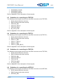
1
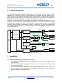
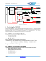
FMC30RF User Manual r1.3 FMC30RF User Manual 4DSP LLC, USA Email: [email protected] This document is the property of 4DSP LLC and may not be copied nor communicated to a third party without the written permission of 4DSP LLC. © 4DSP LLC 2015 UM015 www.4dsp.com -1- FMC30RF User Manual r1.3 Revision History Date Revision Revision 2012-05-30 Draft 0.1 2012-05-30 Release after review 1.0 2012-10-05 Additional info on LNA and reference oscillator 1.1 2014-06-11 Update voltage monitoring section Additional info in Figure 5 and pin out. 1.2 2015-02-12 Added RF input analog line-up description, updated RF in/out characteristics. 1.3 UM015 www.4dsp.com -2- FMC30RF User Manual r1.3 Table of Contents 1 Acronyms and related documents ............................................................................. 4 1.1 Acronyms ................................................................................................................ 4 1.2 Related Documents ................................................................................................. 4 2 General description ..................................................................................................... 5 3 Installation ................................................................................................................... 5 3.1 Requirements and handling instructions .................................................................. 5 4 Design .......................................................................................................................... 6 4.1 Phycisal specifications ............................................................................................ 6 4.1.1 Board Dimensions ............................................................................................ 6 4.1.2 Front panel coax inputs .................................................................................... 6 4.2 Electrical specifications ........................................................................................... 6 4.2.1 EEPROM ......................................................................................................... 7 4.2.2 JTAG................................................................................................................ 7 4.2.3 FMC connector................................................................................................. 7 4.2.4 RF input ........................................................................................................... 7 4.3 Main characteristic .................................................................................................. 9 5 Modes of operation.....................................................................................................10 5.1 Time-Division Duplex (TDD) ...................................................................................10 5.2 Frequency-Division Duplex (FDD) ..........................................................................10 5.3 Multiple-Input Multiple-Output (MIMO) ....................................................................10 6 Controlling the FMC30RF ...........................................................................................11 6.1 Guidelines for controlling the RF path ....................................................................11 6.2 Guidelines for controlling the CDCE62005 .............................................................11 6.3 Guidelines for controlling the TRF3765 ..................................................................12 6.4 Guidelines for controlling the TRF3711 ..................................................................12 6.5 Guidelines for controlling the TRF3720 ..................................................................12 6.6 Guidelines for controlling the AFE7225 ..................................................................12 6.7 Guidelines for controlling the AMC7823 .................................................................13 7 Power supply ..............................................................................................................13 8 Environment................................................................................................................14 8.1 Temperature ..........................................................................................................14 8.2 Monitoring ..............................................................................................................15 8.3 Cooling ...................................................................................................................15 8.3.1 Convection cooling ..........................................................................................15 8.3.2 Conduction cooling ..........................................................................................15 9 Safety...........................................................................................................................16 10 EMC .............................................................................................................................16 11 Ordering information ..................................................................................................16 12 Warranty ......................................................................................................................16 UM015 www.4dsp.com -3- FMC30RF User Manual Appendix A r1.3 LPC pin-out FMC30RF ...............................................................................17 1 Acronyms and related documents 1.1 Acronyms ADC DDR EPROM FBGA FMC FPGA JTAG LED LVTTL LSB LVDS MGT MSB PCB PLL PSSR Analog to Digital Converter Double Data Rate Erasable Programmable Read-Only Memory Fineline Ball Grid Array FPGA Mezzanine Card Field Programmable Gate Array Join Test Action Group Light Emitting Diode Low Voltage Transistor Logic level Least Significant Bit(s) Low Voltage Differential Signaling Multi-Gigabit Transceiver Most Significant Bit(s) Printed Circuit Board Phase Locked Loop Power Supply Rejection Ratio Table 1: Glossary 1.2 Related Documents UM015 FPGA Mezzanine Card (FMC) standard ANSI/VITA 57.1-2010 CDCE62005 datasheet, TI, August 2011 TRF3765 datasheet, TI, November 2011 TRF371109 datasheet, TI, May 2011 TRF371125 datasheet, TI, December 2010 TRF372017 datasheet, TI, August 2010 AMC7823 datasheet, TI, January 2010 www.4dsp.com -4- FMC30RF User Manual r1.3 2 General description The FMC30RF is an FMC Daughter Card which is fully compliant with the VITA 57.1-2010 standard. The FMC30RF offers in a small footprint a low power and fully featured Rx/Tx signal path for the development and deployment of advanced RF solutions. With a frequency range coverage from 400MHz to 3.0GHz (two ranges) and up to 60MHz bandwidth the FMC30RF provides flexibility and reconfigurability to a host of applications. Based on Texas Instruments RF technology the FMC30RF comprises of a dual DAC Tx IQ modulator, a dual ADC Rx IQ demodulator with PGA and LNA front-end and on-board clocking with integrated PLL/VCO. The FMC30RF allows flexible control on sampling frequency through serial communication busses. Furthermore the card is equipped with power supply and temperature monitoring and offers several power-down modes to switch off unused functions. TX VCO IN REF TX CLK TX LO OUT TRF372017 TX_VCO_CTRL AFE7225 LNA_BYPASS_CTRL RF I/O TRF371109 TRF371125 ATT RF IN LO FMC LPC TRX_SWITCH_CTRL LNA_OUT * not avalable from front panel RX VCO IN TRF3765 RX CLK RX LO OUT REF RX_VCO_CTRL TCXO 30.72MHz CDCE65005_REFEN SEC_REF CDCE62005 REF OUT PRI_REF REF IN Figure 1: FMC30RF block diagram 3 Installation 3.1 Requirements and handling instructions UM015 The FMC30RF daughter card must be installed on a carrier card compliant to the FMC standard. The FMC carrier card must support the low-pin count connector (LPC 160-pins). High pin count is permitted. The FMC carrier card must support VADJ/VIO_B voltage between +1.65V and +5.5V. Do not flex the card and prevent electrostatic discharges by observing ESD precautions when handling the card. www.4dsp.com -5- FMC30RF User Manual r1.3 4 Design 4.1 Phycisal specifications 4.1.1 Board Dimensions The FMC30RF card complies with the FMC standard known as ANSI/VITA 57.1. The card is a single width conduction cooled mezzanine module (with region 1 and front panel I/O). A front rib on the carrier hardware is not supported. The stacking height is 10mm. REF IN CDCE 62005 AMC 7823 REF OUT TRF 3765 RX CLK TRF 3711 RF IN AFE 7225 RF I/O TRF 3720 TX CLK Figure 2: FMC30RF dimensions REF IN REF OUT RX CLK RF IN TX CLK RF I/O 4.1.2 Front panel coax inputs The FMC30RF can be ordered with MMCX or SSMC connector type. Six connectors are available on the front panel. Figure 3: FMC30RF bezel layout 4.2 Electrical specifications The FMC30RF card uses a mix of LVDS and LVCMOS signals. According to the FMC standard VADJ should be +2.5V to support LVDS, but the FMC30RF is designed to accept any level on VADJ ranging between 1.65V and 5.5V. VIO_B_M2C connections are connected to VADJ on the FMC30RF. Level translators are implemented to guarantee VADJ level on the FMC connector for all single ended communication and control signals. UM015 www.4dsp.com -6- FMC30RF User Manual r1.3 4.2.1 EEPROM The FMC30RF card carries a 2Kbit EEPROM (24LC02B) which is accessible from the carrier card through the I2C bus. The EEPROM is powered by 3P3VAUX. The standby current is only 0.01µA when SCL and SDA are kept at 3P3VAUX level. These signals may also be left floating since pull-up resistors are present on the card. 4.2.2 JTAG The FMC30RF card TDO pin is connected to the TDI pin (through an SN74LVC1G126 buffer) to ensure continuity of the JTAG chain. TCK, TMS and TRST are left unconnected on the FMC30RF. 4.2.3 FMC connector The low-pin count connector has only bank LA available and two dedicated LVDS clock pairs. The recommendations from AV57.1-2010 Table 14 have been taking into account resulting in the following arrangement: The ADC data clock pair (ADC_DCLKOUT) and ADC frame clock pair (ADC_FCLKOUT) are connected to clock capable pins LA00_CC and LA01_CC respectively. The ADC data pairs are mapped to LA02 to LA05. The DAC clock, frame and data pairs are mapped to LA06 to LA12. Since all pairs are outputs as seen from the FPGA, there is no need to have the clock and frame pair on clock capable pins. LA13 to LA31 are used for low speed single ended communication and control signals. The remaining connections (LA32-LA33) are used left unconnected. An LVDS output of the CDCE62005 is connected to a dedicated LVDS connections on the FMC (CLK0_M2C). The other dedicated LVDS connection is not used. Refer also to the appendix for the detailed LPC connector pinout. 4.2.4 RF input The RF input circuit comprises tuneable and fixed gain stages. The analog line-up is depicted in Figure 4. LNA_BYPASS_CTRL RF I/O AFE7225 TRF371109 TRF371125 BB Gain: 0dB to +24dB ATT RF IN LNA2 +18dB ATT: -1dB to SW3 -32dB -0.5dB SW2 -0.5dB LNA1 +18dB SW1 -0.5dB Figure 4: RF input analog line-up UM015 www.4dsp.com -7- FMC30RF User Manual r1.3 Guidelines of controlling tuneable gain and attenuators are provided in section 6. The maximum input level at the RF input is +3dBm and can be applied to the board when the total gain of the analog line-up is set to minimum. This is done by: - Bypass LNA2 - Set the stepped attenuator to 32dB attenuation - Set the BB gain of the TRF3711 to 0dB (default setting is 15dB, refer to the datasheet of the TRF3711) Applying a signal of +3dBm to the first stage LNA drives the LNA close to its input 1dB compression point. UM015 www.4dsp.com -8- FMC30RF User Manual 4.3 r1.3 Main characteristic RF IN LO Range Low range option: 400MHz – 1200MHz High range option: 1200MHz – 3000MHz Bandwidth 60MHz (when LPF in TRF3711xx bypassed) 50Ω Input Impedance +3dBm1 Maximum Input Level RF OUT LO Range 300MHz – 4800MHz Bandwidth 70MHz 50Ω Output Impedance Full Scale Maximum Output Level +3dBm (depending on LO frequency) Receiver LO (RX CLK) Output Frequency Range Programmable trough fractional PLL (TRF3765): 300MHz to 4800MHz 50Ω Output Impedance -0.5dBm typ. Output Level 300MHz to 4800MHz Input Frequency Range High-impedance Input Impedance 0dBm Input Level Transmitter LO (TX CLK) Output Frequency Range Output Impedance Output Level Input Frequency Range Input Impedance Input Level Programmable trough fractional PLL (TRF372017): 300MHz to 4800MHz 50Ω -0.5dBm typ. 300MHz to 4800MHz High-impedance 0dBm External Reference Input (REF IN) Input Level 0.2VPP - 3.3VPP Input Frequency 10MHz – 250MHz Input Impedance 50Ω External Reference Output (REF OUT) Output Level Output Frequency 3.3VPP (AC coupled LVCMOS) 10MHz – 250MHz Table 2: FMC30RF daughter card main characteristics 1 Make sure minimum gain is configured, refer to section 4.2.4. UM015 www.4dsp.com -9- FMC30RF User Manual r1.3 5 Modes of operation The FMC30RF support different modes of operation; TDD and FDD. TX VCO IN REF TX CLK TX LO OUT TRF372017 TX_VCO_CTRL AFE7225 LNA_BYPASS_CTRL RF I/O TRF371109 TRF371125 ATT RF IN LO FMC LPC TRX_SWITCH_CTRL LNA_OUT * not avalable from front panel RX VCO IN TRF3765 RX CLK RX LO OUT REF RX_VCO_CTRL TCXO 30.72MHz CDCE65005_REFEN SEC_REF CDCE62005 REF OUT PRI_REF REF IN Figure 5: Signal Path 5.1 Time-Division Duplex (TDD) The FMC30RF supports TDD using the RF I/O connector. The RF I/O connector is either receiving (TRX_SWITCH_CTRL=0) or transmitting (TRX_SWITCH_CTRL=1). The TRX_SWITCH_CTRL signal should be driven by the FPGA trough the FMC connector. 5.2 Frequency-Division Duplex (FDD) The FMC30RF supports FDD using the RF I/O connector for transmitting and the RF IN connector for receiving. The TRX_SWITCH_CTRL signal should be driven high by the FPGA trough the FMC connector. 5.3 Multiple-Input Multiple-Output (MIMO) With two FMC30RF boards a 2x2 MIMO setup can be realised. UM015 www.4dsp.com - 10 - FMC30RF User Manual r1.3 TX VCO IN REF TX CLK TX LO OUT TRF372017 TX_VCO_CTRL AFE7225 LNA_BYPASS_CTRL RF I/O TRF371109 TRF371125 ATT RF IN LO FMC LPC TRX_SWITCH_CTRL LNA_OUT * not avalable from front panel RX VCO IN TRF3765 RX CLK RX LO OUT REF RX_VCO_CTRL TCXO 30.72MHz U4P U1P/N CLK_M2C_P/N U2P CDCE65005_REFEN SEC_REF+ CDCE62005 PRI_REF+ U0P/N REF OUT U3P REF IN Figure 6: Clock paths 6 Controlling the FMC30RF Good knowledge of the internal structure and communication protocol of relevant on-board devices is required for controlling the FMC30RF. This document only provides guidelines for programming the devices. For detailed information it is recommended to refer to the datasheets listed in the related documents section of this document. 6.1 Guidelines for controlling the RF path The following control signals controls the RF frontend; TRX_SWITCH_CTRL LNA_BYPASS_CTRL RF_ATT_V[1..5] Refer to Appendix A for a description of these signals. The LNA in the RX path depends on the RF coverage specified at the time of order: - RF coverage option 1 (400MHz – 1200MHz): SKY67101-396LF - RF coverage option 2 (1200MHz – 3000MHz): SKY67100-396LF The gain is 18-20dB for each LNA stage. 6.2 Guidelines for controlling the CDCE62005 The following control signals connect from the FMC connector to the CDCE62005; SCLK (shared with other devices) SDATA (shared with other devices) CDCE62005_CS# CDCE62005_SDOUT CDCE62005_PD# UM015 www.4dsp.com - 11 - FMC30RF User Manual r1.3 CDCE62005_SYNC# CDCE62005_LOCK CDCE62005_REFEN Refer to Appendix A for a description of these signals. 6.3 Guidelines for controlling the TRF3765 The following control signals connect from the FMC connector to the TRF3765; SCLK (shared with other devices) SDATA (shared with other devices) TRF3765_CS# TRF3765_SDOUT TRF3765_LOCK RX_VCO_CTRL Refer to Appendix A for a description of these signals. 6.4 Guidelines for controlling the TRF3711 The following control signals connect from the FMC connector to the TRF3711; SCLK (shared with other devices) SDATA (shared with other devices) TRF3711_CS# TRF3711_SDOUT TRF3711_PD# TRF3711_GAIN_B[0..2] Refer to Appendix A for a description of these signals. 6.5 Guidelines for controlling the TRF3720 The following control signals connect from the FMC connector to the TRF3720; SCLK (shared with other devices) SDATA (shared with other devices) TRF3720_CS# TRF3720_SDOUT TRF3720_PS TRF3720_LOCK TX_VCO_CTRL Refer to Appendix A for a description of these signals. 6.6 Guidelines for controlling the AFE7225 The following control signals connect from the FMC connector to the AFE7225; SCLK (shared with other devices) SDATA (shared with other devices) AFE7225_CS# UM015 www.4dsp.com - 12 - FMC30RF User Manual r1.3 AFE7225_SDOUT AFE7225_RESET AFE7225_PD Refer to Appendix A for a description of these signals. 6.7 Guidelines for controlling the AMC7823 The following control signals connect from the FMC connector to the AMC7823; SCLK (shared with other devices) SDATA (shared with other devices) AMC7823_CS# AMC7823_SDOUT AMC7823_GALR# AMC7823_RESET# Refer to Appendix A for a description of these signals. 7 Power supply Power is supplied to the FMC30RF card through the FMC connector. The pin current rating is 2.7A, but the overall maximum as specified by the FMC standard is limited according to Table 3. Voltage +3.3V +12V VADJ (+2.5V) VIO_B (+2.5V) # pins 4 2 4 2 Max Amps 3A 1A 4A 1.15 A Max Watt 10 W 12 W 10 W 2.3 W Table 3: FMC standard power specification The power provided by the carrier card can be very noisy. Special care is taken with the power supply generation on the FMC30RF card to minimize the effect of power supply noise on clock generation, (de-)modulation, and data conversion. Clean supply is derived from +3.3V and 12V in two steps for maximum efficiency. The first step uses a high efficient switched regulators to generate +3.8V and +5.5V power rails. From these power rail the analog and digital supplies are derived with a low dropout, low noise, high PSRR, linear regulator. At several stages in the power supply there is additional noise filtering with beads and capacitance. Power supplies for different devices are isolated where necessary. UM015 www.4dsp.com - 13 - FMC30RF User Manual r1.3 Power plane VADJ 3P3V 12P0V 3P3VAUX (Operating) 3P3VAUX (Standby) Typical 100mA 1.3A 0.5A 0.1 mA 0.01 µA Maximum 200mA 1.6A 0.6A 3 mA 1 µA Table 4: Typical/Maximum current drawn from FMC carrier card 5.5V 1.4A @ 3.3V 0.5A @ 12V 3.8V TPS63020 (0.75A) 3.3V à 5.5V TPS5430 (1.30A) 12V à 3.8V Typical power consumption: 10 Watt TPS7A8001 (60mA) 3.8V à 1.8V VDD1_1p8 TPS7A8001 (60mA) 3.8V à 1.8V VDD2_1p8 TPS7A8001 (40mA) 5.5V à 5.0V 5V0A_DAC TPS7A8001 (132mA) 3.8V à 3.3V 3V3A_DAC TPS7A8001 (580mA) 3.8V à 3.3V CDCE_3p3 TPS7A8001 (30mA) 3.8V à 3.3V TCXO_3p3 TPS7A8001 (201mA) 5.5V à 4.0V RF_4p0 TPS7A8001 (360mA) 5.5V à 5.0V TRF3711_5p0 TPS74401(148mA) 5.5V à 5.0V TRF3720_5p0 TPS74401 (250mA) 3.8V à 3.3V TRF3720_3p3 TPS74401 (190mA) 3.8V à 3.3V TRF3765_3p3 Figure 7: FMC30RF Power Supply Architecture 8 Environment 8.1 Temperature Operating temperature: -40°C to +85°C (Industrial) UM015 www.4dsp.com - 14 - FMC30RF User Manual r1.3 Storage temperature: -40°C to +120°C 8.2 Monitoring The AMC7823 device may be used to monitor the voltage on the different power rails as well as the temperature. It is recommended that the carrier card and/or host software uses the power-down features in the devices in the case the temperature is too high. Normal operations can resume once the temperature is within the operating conditions boundaries. Parameter: Voltage Formula Channel 0 5.0V Analog DAC 2 * ADC0 Channel 1 3.3V Digital/Clock 2 * ADC1 Channel 2 1.8V Analog/Digital 2 * ADC2 Channel 3 4.0V RF 2 * ADC3 Channel 4 5.0V Analog 2 * ADC4 Channel 5 3.3V Analog 2 * ADC5 Channel 6 3.3V TCXO 2 * ADC6 Channel 7 VADJ 2 * ADC7 Temperature (Ch 8) Table 5: Temperature and voltage parameters 8.3 Cooling Two different types of cooling will be available for the FMC30RF. 8.3.1 Convection cooling The air flow provided by the chassis fans the FMC30RF is enclosed in will dissipate the heat generated by the on board components. A minimum airflow of 300 LFM is recommended. For stand alone operations (such as on a Xilinx development kit), it is highly recommended to blow air across the FMC and ensure that the temperature of the devices is within the allowed range. 4DSP’s warranty does not cover boards on which the maximum allowed temperature has been exceeded. 8.3.2 Conduction cooling In demanding environments, the ambient temperature inside a chassis could be close to the operating temperature defined in this document. It is very likely that in these conditions the junction temperature of power consuming devices will exceed the operating conditions recommended by the devices manufacturers (mostly +85°C). The FMC30RF is designed for maximum heat transfer to conduction cooled ribs. A customized cooling frame that connects directly to the surface of the devices is allowed (contact 4DSP for detailed mechanical information). UM015 www.4dsp.com - 15 - FMC30RF User Manual r1.3 9 Safety This module presents no hazard to the user. 10 EMC This module is designed to operate from within an enclosed host system, which is build to provide EMC shielding. Operation within the EU EMC guidelines is not guaranteed unless it is installed within an adequate host system. This module is protected from damage by fast voltage transients originating from outside the host system which may be introduced through the system. 11 Ordering information Part Number: FMC30RF-2-1-1-1 Card Type FMC30RF Temperature Range Industrial (-40oC to +85oC) = 1 Commercial (0oC to +70oC) = 2 Connector Type Standard Feature – MMCX (snap coupling) = 1 SSMC (screw coupling) = 2 RF coverage 400MHz – 1200MHz = 1 1200MHz – 3000MHz = 2 Mil-I-46058c Conformal Coating No Conformal Coating = 1 Add Conformal Coating = 2 12 Warranty Hardware Software/Firmware Basic Warranty (included) 1 Year from Date of Shipment 90 Days from Date of Shipment Extended Warranty (optional) 2 Years from Date of Shipment 1 Year from Date of Shipment UM015 www.4dsp.com - 16 - Appendix A LPC pin-out FMC30RF FMC label FMC30RF Signal Description CLK0_M2C_N CLK_TO_FPGA_N Output from CDCE62005 CLK0_M2C_P CLK_TO_FPGA_P Output from CDCE62005 LA00_N_CC ADC_DCLKOUT_N Connects to AFE7225 LA00_P_CC ADC_DCLKOUT_P Connects to AFE7225 LA01_N_CC ADC_FCLKOUT_N Connects to AFE7225 LA01_P_CC ADC_FCLKOUT_P Connects to AFE7225 LA02_N ADCB_DATA1_N Connects to AFE7225 LA02_P ADCB_DATA1_P Connects to AFE7225 LA03_N ADCB_DATA0_N Connects to AFE7225 LA03_P ADCB_DATA0_P Connects to AFE7225 LA04_N ADCA_DATA1_N Connects to AFE7225 LA04_P ADCA_DATA1_P Connects to AFE7225 LA05_N ADCA_DATA0_N Connects to AFE7225 LA05_P ADCA_DATA0_P Connects to AFE7225 LA06_N DAC_FCLKIN_N Connects to AFE7225 LA06_P DAC_FCLKIN_P Connects to AFE7225 LA07_N DACA_DATA1_N Connects to AFE7225 LA07_P DACA_DATA1_P Connects to AFE7225 LA08_N DACA_DATA0_N Connects to AFE7225 LA08_P DACA_DATA0_P Connects to AFE7225 LA09_N DACB_DATA0_N Connects to AFE7225 LA09_P DACB_DATA0_P Connects to AFE7225 LA10_N DAC_DCLKIN_N Connects to AFE7225 LA10_P DAC_DCLKIN_P Connects to AFE7225 LA11_N DAC_SYNCIN_N Connects to AFE7225 LA11_P DAC_SYNCIN_P Connects to AFE7225 LA12_N DACB_DATA1_N Connects to AFE7225 LA12_P DACB_DATA1_P Connects to AFE7225 LA13_N LNA_BYPASS_CTRL ‘0’ = 2nd LNA is excluded from the RX path ‘1’ = 2nd LNA is included in the RX path LA13_P TRX_SWITCH_CTRL Behavior on RF I/O connector; ‘0’ = RF I/O connector is receiving (RX) ‘1’ = RF I/O connector is transmitting (TX) Behavior on RF IN connector; ‘0’ = RF IN connector is disconnected ‘1’ = RF IN connector is receiving (RX) LA14_N RF_ATT_V1 Connects to SKY12329-350LF V1 LA14_P RF_ATT_V2 Connects to SKY12329-350LF V2 LA15_N TRF3765_CS# Connects to TRF3765 STROBE FMC30RF User Manual r1.3 LA15_P AFE7225_RESET Connects to AFE7225 RESET LA16_N AFE7225_CS# Connects to AFE7225 SEN LA16_P AFE7225_PD Connects to AFE7225 PDN LA17_N_CC RF_ATT_V4 Connects to SKY12329-350LF V4 LA17_P_CC RF_ATT_V3 Connects to SKY12329-350LF V3 LA18_N_CC AMC7823_CS# Connects to AMC7823 SS LA18_P_CC AMC7823_RESET# Connects to AMC7823 RESET LA19_N CDCE62005_LOCK Connects to CDCE62005 PLL_LOCK LA19_P TRF3765_LOCK Connects to TRF3765 LD LA20_N RF_ATT_V5 Connects to SKY12329-350LF V5 LA20_P TRF3720_LOCK Connects to TRF3720 LD LA21_N SCLK Connects to: - CDCE62005 SPI_CLK - TRF3765 CLOCK - TRF3720 CLK - TRF3711 CLOCK - AFE7225 SCLK - AMC7823 SCLK LA21_P TRF3720_CS# Connects to TRF3720 LE LA22_N RX_VCO_CTRL Behavior on RX CLK connector; ‘0’ = RX CLK connector is VCO output from TRF3765 LO4_OUT ‘1’ = RX CLK connector is VCO input to TRF3765 EXTVCO_IN LA22_P TRF3720_PS Connects to TRF3720 PS LA23_N TX_VCO_CTRL Behavior on TX CLK connector; ‘0’ = TX CLK connector is VCO output from TRF3720 LO_OUT ‘1’ = TX CLK connector is VCO input to TRF3720 EXT_VCO LA23_P TRF3711_PD# Connects to TRF3711 CHIP_EN LA24_N TRF3711_CS# Connects to TRF3711 STROBE LA24_P SDATA Connects to - CDCE62005 MOSI - TRF3765 DATA - TRF3720 DATA - TRF3711 DATA - AFE7225 SDATA - AMC7823 MOSI LA25_N TRF3711_GAIN_B0 Connects to TRF3711 GAIN_B0 LA25_P TRF3711_GAIN_B1 Connects to TRF3711 GAIN_B1 LA26_N CDCE62005_REFEN Behavior on on-board reference clock; ‘0’ = the on-board reference clock is powered down ‘1’ = the on-board reference clock is enabled LA26_P TRF3711_GAIN_B2 Connects to TRF3711 GAIN_B2 LA27_N CDCE62005_SDOUT Connects to CDCE62005 MISO LA27_P AFE7225_SDOUT Connects to AFE7225 SDOUT LA28_N CDCE62005_PD# Connects to CDCE62005 POWER_DOWN LA28_P CDCE62005_SYNC# Connects to CDCE62005 SYNC LA29_N TRF3720_SDOUT Connects to TRF3720 RDBK UM015 www.4dsp.com - 18 - FMC30RF User Manual r1.3 LA29_P TRF3711_SDOUT Connects to TRF3711 READBACK LA30_N AMC7823_SDOUT Connects to AMC7823 MISO LA30_P CDCE62005_CS# Connects to CDCE62005 SPI_LE LA31_N AMC7823_GALR# Connects to AMC7823 GALR# LA31_P TRF3765_SDOUT Connects to TRF3765 READBACK LA32_N Not connected LA32_P Not connected LA33_N Not connected LA33_P Not connected PRSNT_M2C_L PRSNT_M2C_L Connects to GND PG_C2M PG_C2M Connects to PS_EN UM015 www.4dsp.com - 19 -