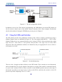
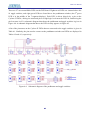
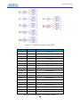
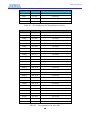
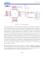
1
Altera DE2 Board
DE2
Development and Education Board
User Manual
Version 1.4
Copyright © 2006 Altera Corporation
Altera DE2 Board
CONTENTS
Chapter 1 DE2 Package.....................................................................................................................1
1.1
1.2
1.3
Package Contents .................................................................................................................1
The DE2 Board Assembly....................................................................................................2
Getting Help.........................................................................................................................3
Chapter 2 Altera DE2 Board.............................................................................................................4
2.1
2.2
2.3
Layout and Components ......................................................................................................4
Block Diagram of the DE2 Board........................................................................................5
Power-up the DE2 Board .....................................................................................................9
Chapter 3 DE2 Control Panel .........................................................................................................10
3.1
3.2
3.3
3.4
3.5
3.6
3.7
Control Panel Setup ........................................................................................................... 11
Controlling the LEDs, 7-Segment Displays and LCD Display .........................................13
SDRAM/SRAM Controller and Programmer....................................................................14
Flash Memory Programmer ...............................................................................................16
Overall Structure of the DE2 Control Panel ......................................................................17
TOOLS – Multi-Port SRAM/SDRAM/Flash Controller ...................................................19
VGA Display Control.........................................................................................................20
Chapter 4 Using the DE2 Board .....................................................................................................24
4.1
4.2
4.3
4.4
4.5
4.6
4.7
4.8
4.9
4.10
4.11
4.12
4.13
4.14
4.15
4.16
Configuring the Cyclone II FPGA .....................................................................................24
Using the LEDs and Switches............................................................................................26
Using the 7-segment Displays............................................................................................30
Clock Inputs .......................................................................................................................32
Using the LCD Module......................................................................................................33
Using the Expansion Header..............................................................................................35
Using VGA ........................................................................................................................37
Using the 24-bit Audio CODEC ........................................................................................41
RS-232 Serial Port .............................................................................................................42
PS/2 Serial Port ..................................................................................................................42
Fast Ethernet Network Controller ......................................................................................43
TV Decoder........................................................................................................................44
Implementing a TV Encoder..............................................................................................46
Using USB Host and Device..............................................................................................46
Using IrDA.........................................................................................................................48
Using SDRAM/SRAM/Flash.............................................................................................49
Chapter 5 Examples of Advanced Demonstrations ......................................................................54
5.1
DE2 Factory Configuration................................................................................................54
ii
Altera DE2 Board
5.2
5.3
5.4
5.5
5.6
5.7
5.8
TV Box Demonstration......................................................................................................55
USB Paintbrush..................................................................................................................57
USB Device........................................................................................................................59
A Karaoke Machine ...........................................................................................................61
Ethernet Packet Sending/Receiving ...................................................................................62
SD Card Music Player........................................................................................................64
Music Synthesizer Demonstration .....................................................................................66
iii
DE2 User Manual
Chapter 1
DE2 Package
The DE2 package contains all components needed to use the DE2 board in conjunction with a
computer that runs the Microsoft Windows software.
1.1 Package Contents
Figure 1.1 shows a photograph of the DE2 package.
Figure 1.1. The DE2 package contents.
1
DE2 User Manual
The DE2 package includes:
•
•
•
DE2 board
USB Cable for FPGA programming and control
CD-ROM containing the DE2 documentation and supporting materials, including the User
Manual, the Control Panel utility, reference designs and demonstrations, device datasheets,
tutorials, and a set of laboratory exercises
•
CD-ROMs containing Altera’s Quartus® II Web Edition and the Nios® II Embedded Design
Suit Evaluation Edition software.
•
Bag of six rubber (silicon) covers for the DE2 board stands. The bag also contains some
extender pins, which can be used to facilitate easier probing with testing equipment of the
board’s I/O expansion headers
•
•
Clear plastic cover for the board
9V DC wall-mount power supply
1.2 The DE2 Board Assembly
To assemble the included stands for the DE2 board:
•
Assemble a rubber (silicon) cover, as shown in Figure 1.2, for each of the six copper stands
on the DE2 board
•
The clear plastic cover provides extra protection, and is mounted over the top of the board
by using additional stands and screws
Figure 1.2. The feet for the DE2 board.
2
DE2 User Manual
1.3 Getting Help
Here are the addresses where you can get help if you encounter problems:
•
Altera Corporation
101 Innovation Drive
San Jose, California, 95134 USA
Email: [email protected]
•
Terasic Technologies
No. 356, Sec. 1, Fusing E. Rd.
Jhubei City, HsinChu County, Taiwan, 302
Email: [email protected]
Web: DE2.terasic.com
•
Arches Computing
Unit 708-222 Spadina Ave
Toronto, Ontario, Canada M5T3A2
Email: [email protected]
Web: DE2.archescomputing.com
A BBS (Bulletin Board System) Forum for the DE2 board has been created at the address shown
below. This Forum is meant to serve as a repository for information about the DE2 board, and to
provide a resource through which users can ask questions, and share design examples.
•
BBS forum: http://www.terasic.com/english/discuss.htm
3
DE2 User Manual
Chapter 2
Altera DE2 Board
This chapter presents the features and design characteristics of the DE2 board.
2.1 Layout and Components
A photograph of the DE2 board is shown in Figure 2.1. It depicts the layout of the board and
indicates the location of the connectors and key components.
Figure 2.1. The DE2 board.
The DE2 board has many features that allow the user to implement a wide range of designed
circuits, from simple circuits to various multimedia projects.
The following hardware is provided on the DE2 board:
•
Altera Cyclone® II 2C35 FPGA device
•
•
Altera Serial Configuration device - EPCS16
USB Blaster (on board) for programming and user API control; both JTAG and Active Serial
(AS) programming modes are supported
•
•
512-Kbyte SRAM
8-Mbyte SDRAM
4
DE2 User Manual
•
•
•
•
•
•
•
•
•
•
•
•
•
•
•
•
4-Mbyte Flash memory (1 Mbyte on some boards)
SD Card socket
4 pushbutton switches
18 toggle switches
18 red user LEDs
9 green user LEDs
50-MHz oscillator and 27-MHz oscillator for clock sources
24-bit CD-quality audio CODEC with line-in, line-out, and microphone-in jacks
VGA DAC (10-bit high-speed triple DACs) with VGA-out connector
TV Decoder (NTSC/PAL) and TV-in connector
10/100 Ethernet Controller with a connector
USB Host/Slave Controller with USB type A and type B connectors
RS-232 transceiver and 9-pin connector
PS/2 mouse/keyboard connector
IrDA transceiver
Two 40-pin Expansion Headers with diode protection
In addition to these hardware features, the DE2 board has software support for standard I/O
interfaces and a control panel facility for accessing various components. Also, software is provided
for a number of demonstrations that illustrate the advanced capabilities of the DE2 board.
In order to use the DE2 board, the user has to be familiar with the Quartus II software. The
necessary knowledge can be acquired by reading the tutorials Getting Started with Altera’s DE2
Board and Quartus II Introduction (which exists in three versions based on the design entry method
used, namely Verilog, VHDL or schematic entry). These tutorials are provided in the directory
DE2_tutorials on the DE2 System CD-ROM that accompanies the DE2 board and can also be
found on Altera’s DE2 web pages.
2.2 Block Diagram of the DE2 Board
Figure 2.2 gives the block diagram of the DE2 board. To provide maximum flexibility for the user,
all connections are made through the Cyclone II FPGA device. Thus, the user can configure the
FPGA to implement any system design.
5
DE2 User Manual
Figure 2.2. Block diagram of the DE2 board.
Following is more detailed information about the blocks in Figure 2.2:
Cyclone II 2C35 FPGA
•
•
•
•
•
•
•
33,216 LEs
105 M4K RAM blocks
483,840 total RAM bits
35 embedded multipliers
4 PLLs
475 user I/O pins
FineLine BGA 672-pin package
Serial Configuration device and USB Blaster circuit
•
•
•
Altera’s EPCS16 Serial Configuration device
On-board USB Blaster for programming and user API control
JTAG and AS programming modes are supported
6
DE2 User Manual
SRAM
•
•
•
512-Kbyte Static RAM memory chip
Organized as 256K x 16 bits
Accessible as memory for the Nios II processor and by the DE2 Control Panel
SDRAM
•
•
•
8-Mbyte Single Data Rate Synchronous Dynamic RAM memory chip
Organized as 1M x 16 bits x 4 banks
Accessible as memory for the Nios II processor and by the DE2 Control Panel
Flash memory
•
•
•
4-Mbyte NOR Flash memory (1 Mbyte on some boards)
8-bit data bus
Accessible as memory for the Nios II processor and by the DE2 Control Panel
SD card socket
•
•
Provides SPI mode for SD Card access
Accessible as memory for the Nios II processor with the DE2 SD Card Driver
Pushbutton switches
•
•
•
4 pushbutton switches
Debounced by a Schmitt trigger circuit
Normally high; generates one active-low pulse when the switch is pressed
Toggle switches
•
•
18 toggle switches for user inputs
A switch causes logic 0 when in the DOWN (closest to the edge of the DE2 board) position
and logic 1 when in the UP position
Clock inputs
•
•
•
50-MHz oscillator
27-MHz oscillator
SMA external clock input
7
DE2 User Manual
Audio CODEC
•
•
•
•
Wolfson WM8731 24-bit sigma-delta audio CODEC
Line-level input, line-level output, and microphone input jacks
Sampling frequency: 8 to 96 KHz
Applications for MP3 players and recorders, PDAs, smart phones, voice recorders, etc.
VGA output
•
•
•
•
Uses the ADV7123 240-MHz triple 10-bit high-speed video DAC
With 15-pin high-density D-sub connector
Supports up to 1600 x 1200 at 100-Hz refresh rate
Can be used with the Cyclone II FPGA to implement a high-performance TV Encoder
NTSC/PAL TV decoder circuit
•
•
•
•
•
•
Uses ADV7181B Multi-format SDTV Video Decoder
Supports NTSC-(M,J,4.43), PAL-(B/D/G/H/I/M/N), SECAM
Integrates three 54-MHz 9-bit ADCs
Clocked from a single 27-MHz oscillator input
Supports Composite Video (CVBS) RCA jack input.
Supports digital output formats (8-bit/16-bit): ITU-R BT.656 YCrCb 4:2:2 output + HS, VS,
and FIELD
•
Applications: DVD recorders, LCD TV, Set-top boxes, Digital TV, Portable video devices
10/100 Ethernet controller
•
•
•
•
•
•
Integrated MAC and PHY with a general processor interface
Supports 100Base-T and 10Base-T applications
Supports full-duplex operation at 10 Mb/s and 100 Mb/s, with auto-MDIX
Fully compliant with the IEEE 802.3u Specification
Supports IP/TCP/UDP checksum generation and checking
Supports back-pressure mode for half-duplex mode flow control
USB Host/Slave controller
•
•
•
•
Complies fully with Universal Serial Bus Specification Rev. 2.0
Supports data transfer at full-speed and low-speed
Supports both USB host and device
Two USB ports (one type A for a host and one type B for a device)
•
Provides a high-speed parallel interface to most available processors; supports Nios II with a
Terasic driver
8
DE2 User Manual
•
Supports Programmed I/O (PIO) and Direct Memory Access (DMA)
Serial ports
•
•
•
•
One RS-232 port
One PS/2 port
DB-9 serial connector for the RS-232 port
PS/2 connector for connecting a PS2 mouse or keyboard to the DE2 board
IrDA transceiver
•
•
•
•
•
Contains a 115.2-kb/s infrared transceiver
32 mA LED drive current
Integrated EMI shield
IEC825-1 Class 1 eye safe
Edge detection input
Two 40-pin expansion headers
•
72 Cyclone II I/O pins, as well as 8 power and ground lines, are brought out to two 40-pin
expansion connectors
•
•
40-pin header is designed to accept a standard 40-pin ribbon cable used for IDE hard drives
Diode and resistor protection is provided
2.3 Power-up the DE2 Board
The DE2 board comes with a preloaded configuration bit stream to demonstrate some features of
the board. This bit stream also allows users to see quickly if the board is working properly. To
power-up the board perform the following steps:
1. Connect the provided USB cable from the host computer to the USB Blaster connector on
the DE2 board. For communication between the host and the DE2 board, it is necessary to
install the Altera USB Blaster driver software. If this driver is not already installed on the
host computer, it can be installed as explained in the tutorial Getting Started with Altera's
2.
3.
4.
5.
DE2 Board. This tutorial is available on the DE2 System CD-ROM and from the Altera
DE2 web pages.
Connect the 9V adapter to the DE2 board
Connect a VGA monitor to the VGA port on the DE2 board
Connect your headset to the Line-out audio port on the DE2 board
Turn the RUN/PROG switch on the left edge of the DE2 board to RUN position; the
PROG position is used only for the AS Mode programming
9
DE2 User Manual
6. Turn the power on by pressing the ON/OFF switch on the DE2 board
At this point you should observe the following:
•
•
•
•
•
•
All user LEDs are flashing
All 7-segment displays are cycling through the numbers 0 to F
The LCD display shows Welcome to the Altera DE2 Board
The VGA monitor displays the image shown in Figure 2.3.
Set the toggle switch SW17 to the DOWN position; you should hear a 1-kHz sound
Set the toggle switch SW17 to the UP position and connect the output of an audio player to
the Line-in connector on the DE2 board; on your headset you should hear the music played
from the audio player (MP3, PC, iPod, or the like)
•
You can also connect a microphone to the Microphone-in connector on the DE2 board; your
voice will be mixed with the music played from the audio player
Figure 2.3. The default VGA output pattern.
Chapter 3
10
DE2 User Manual
DE2 Control Panel
The DE2 board comes with a Control Panel facility that allows a user to access various components
on the board through a USB connection from a host computer. This chapter first presents some
basic functions of the Control Panel, then describes its structure in block diagram form, and finally
describes its capabilities.
3.1 Control Panel Setup
To run the Control Panel application, it is first necessary to configure a corresponding circuit in the
Cyclone II FPGA. This is done by downloading the configuration file DE2_USB_API.sof into the
FPGA. The downloading procedure is described in Section 4.1.
In addition to the DE2_USB_API.sof file, it is necessary to execute on the host computer the
program DE2_control_panel.exe. Both of these files are available on the DE2 System CD-ROM
that accompanies the DE2 board, in the directory DE2_control_panel. Of course, these files may
already have been installed to some other location on your computer system.
To activate the Control Panel, perform the following steps:
1. Connect the supplied USB cable to the USB Blaster port, connect the 9V power supply,
and turn the power switch ON
2. Set the RUN/PROG switch to the RUN position
3. Start the Quartus II software
4. Select Tools > Programmer to reach the window in Figure 3.1. Click on Add File and in
the pop-up window that appears select the DE2_USB_API.sof file. Next, click on the
Program/Configure box which results in the image displayed in the figure. Now, click
Start to download the configuration file into the FPGA.
5. Start the executable DE2_control_panel.exe on the host computer. The Control Panel user
interface shown in Figure 3.2 will appear.
6. Open the USB port by clicking Open > Open USB Port 0. The DE2 Control Panel
application will list all the USB ports that connect to DE2 boards. The DE2 Control Panel
can control up to 4 DE2 boards using the USB links. The Control Panel will occupy the
USB port until you close that port; you cannot use Quartus II to download a configuration
file into the FPGA until you close the USB port.
7. The Control Panel is now ready for use; experiment by setting the value of some 7-segment
display and observing the result on the DE2 board.
11
DE2 User Manual
Figure 3.1. Quartus II Programmer window.
Figure 3.2. The DE2 Control Panel.
The concept of the DE2 Control Panel is illustrated in Figure 3.3. The IP that performs the control
functions is implemented in the FPGA device. It communicates with the Control Panel window,
which is active on the host computer, via the USB Blaster link. The graphical interface is used to
issue commands to the control circuitry. The provided IP handles all requests and performs data
transfers between the computer and the DE2 board.
12
DE2 User Manual
Figure 3.3. The DE2 Control Panel concept.
The DE2 Control Panel can be used to change the values displayed on 7-segment displays, light up
LEDs, talk to the PS/2 keyboard, read/write the SRAM, Flash Memory and SDRAM, load an image
pattern to display as VGA output, load music to the memory and play music via the audio DAC.
The feature of reading/writing a byte or an entire file from/to the Flash Memory allows the user to
develop multimedia applications (Flash Audio Player, Flash Picture Viewer) without worrying about
how to build a Flash Memory Programmer.
3.2 Controlling the LEDs, 7-Segment Displays and LCD Display
A simple function of the Control Panel is to allow setting the values displayed on LEDs, 7-segment
displays, and the LCD character display.
In the window shown in Figure 3.2, the values to be displayed by the 7-segment displays (which are
named HEX7-0) can be entered into the corresponding boxes and displayed by pressing the Set
button. A keyboard connected to the PS/2 port can be used to type text that will be displayed on the
LCD display.
Choosing the LED & LCD tab leads to the window in Figure 3.4. Here, you can turn the individual
LEDs on by selecting them and pressing the Set button. Text can be written to the LCD display by
typing it in the LCD box and pressing the corresponding Set button.
The ability to set arbitrary values into simple display devices is not needed in typical design
activities. However, it gives the user a simple mechanism for verifying that these devices are
functioning correctly in case a malfunction is suspected. Thus, it can be used for troubleshooting
purposes.
13
DE2 User Manual
Figure 3.4. Controlling LEDs and the LCD display.
3.3 SDRAM/SRAM Controller and Programmer
The Control Panel can be used to write/read data to/from the SDRAM and SRAM chips on the DE2
board. We will describe how the SDRAM may be accessed; the same approach is used to access the
SRAM. Click on the SDRAM tab to reach the window in Figure 3.5.
Figure 3.5. Accessing the SDRAM.
14
DE2 User Manual
A 16-bit word can be written into the SDRAM by entering the address of the desired location,
specifying the data to be written, and pressing the Write button. Contents of the location can be
read by pressing the Read button. Figure 3.5 depicts the result of writing the hexadecimal value
6CA into location 200, followed by reading the same location.
The Sequential Write function of the Control Panel is used to write the contents of a file into the
SDRAM as follows:
1. Specify the starting address in the Address box.
2. Specify the number of bytes to be written in the Length box. If the entire file is to be
loaded, then a checkmark may be placed in the File Length box instead of giving the
number of bytes.
3. To initiate the writing of data, click on the Write a File to SDRAM button.
4. When the Control Panel responds with the standard Windows dialog box asking for the
source file, specify the desired file in the usual manner.
The Control Panel also supports loading files with a .hex extension. Files with a .hex extension are
ASCII text files that specify memory values using ASCII characters to represent hexadecimal
values. For example, a file containing the line
0123456789ABCDEF
defines four 16-bit values: 0123, 4567, 89AB, CDEF. These values will be loaded consecutively
into the memory.
The Sequential Read function is used to read the contents of the SDRAM and place them into a file
as follows:
1. Specify the starting address in the Address box.
2. Specify the number of bytes to be copied into the file in the Length box. If the entire
contents of the SDRAM are to be copied (which involves all 8 Mbytes), then place a
checkmark in the Entire SDRAM box.
3. Press Load SDRAM Content to a File button.
4. When the Control Panel responds with the standard Windows dialog box asking for the
destination file, specify the desired file in the usual manner.
15
DE2 User Manual
3.4 Flash Memory Programmer
The Control Panel can be used to write/read data to/from the Flash memory chip on the DE2 board.
It can be used to:
•
•
•
•
•
Erase the entire Flash memory
Write one byte to the memory
Read one byte from the memory
Write a binary file to the memory
Load the contents of the Flash memory into a file
Note the following characteristics of the Flash memory:
•
•
The Flash memory chip is organized as 4 M (or 1 M on some boards) x 8 bits.
You must erase the entire Flash memory before you can write into it. (Be aware that the
number of times a Flash memory can be erased is limited.)
•
The time required to erase the entire Flash memory is about 20 seconds. Do not close the
DE2 Control Panel in the middle of the operation.
To open the Flash memory control window, shown in Figure 3.6, select the FLASH tab in the
Control Panel.
Figure 3.6. Flash memory control window.
A byte of data can be written into a random location on the Flash chip as follows:
1. Click on the Chip Erase button. The button and the window frame title will prompt you to
wait until the operation is finished, which takes about 20 seconds.
16
DE2 User Manual
2. Enter the desired address into the Address box and the data byte into the wDATA box.
Then, click on the Write button.
To read a byte of data from a random location, enter the address of the location and click on the
Read button. The rDATA box will display the data read back from the address specified.
The Sequential Write function is used to load a file into the Flash chip as follows:
1. Specify the starting address and the length of data (in bytes) to be written into the Flash
memory. You can click on the File Length checkbox to indicate that you want to load the
entire file.
2. Click on the Write a File to Flash button to activate the writing process.
3. When the Control Panel responds with the standard Windows dialog box asking for the
source file, specify the desired file in the usual manner.
The Sequential Read function is used to read the data stored in the Flash memory and write this data
into a file as follows:
1. Specify the starting address and the length of data (in bytes) to be read from the Flash
memory. You can click on the Entire Flash checkbox to indicate that you want to copy the
entire contents of the Flash memory into a specified file.
2. Click on the Load Flash Content to a File button to activate the reading process.
3. When the Control Panel responds with the standard Windows dialog box asking for the
destination file, specify the desired file in the usual manner.
3.5 Overall Structure of the DE2 Control Panel
The DE2 Control Panel facility communicates with a circuit that is instantiated in the Cyclone II
FPGA. This circuit is specified in Verilog code, which makes it possible for a knowledgeable user
to change the functionality of the Control Panel. The code is located inside the DE2_demonstrations
directory on the DE2 System CD-ROM.
To run the Control Panel, the user must first set it up as explained in Section 3.1. Figure 3.7 depicts
the structure of the Control Panel. Each input/output device is controlled by a controller instantiated
in the FPGA chip. The communication with the PC is done via the USB Blaster link. A Command
Controller circuit interprets the commands received from the PC and performs the appropriate
actions. The SDRAM, SRAM, and Flash Memory controllers have three user-selectable
asynchronous ports in addition to the Host port that provides a link with the Command Controller.
The connection between the VGA DAC Controller and the FPGA memory allows displaying of the
default image shown on the left side of the figure, which is stored in an M4K block in the Cyclone
17
DE2 User Manual
II chip. The connection between the Audio DAC Controller and a lookup table in the FPGA is used
to produce a test audio signal of 1 kHz.
To let users implement and test their IP cores (written in Verilog) without requiring them to
implement complex API/Host control software and memory (SRAM/SDRAM/Flash) controllers,
we provide an integrated control environment consisting of a software controller in C++, a USB
command controller, and a multi-port SRAM/SDRAM/Flash controller.
Figure 3.7. The DE2 Control Panel block diagram.
Users can connect circuits of their own design to one of the User Ports of the SRAM/SDRAM/Flash
controller. Then, they can download binary data into the SRAM/SDRAM/Flash. Once the data is
downloaded to the SDRAM/Flash, users can configure the memory controllers so that their circuits
can read/write the SDRAM/Flash via the User Ports connected.
18
DE2 User Manual
3.6 TOOLS – Multi-Port SRAM/SDRAM/Flash Controller
The TOOLS page of the Control Panel GUI allows selection of the User Ports. We will illustrate a
typical process by implementing a Flash Music Player. The music data is loaded into the Flash
memory. User Port 1 in the Flash Controller is used to send the music data to the Audio DAC
Controller and hence to the audio output jack.
You can implement this application as follows:
1. Erase the Flash memory (as explained in Section 3.4). Then, write a music file into the
Flash memory. You can use the file music.wav in the directory DE2_demonstrations\music
on the DE2 System CD-ROM.
2. In the DE2 Control Panel, select the TOOLS tab to reach the window in Figure 3.8.
Figure 3.8. TOOLS window of the DE2 Control Panel.
3. Select the Asynchronous 1 port for the Flash Multiplexer and then click on the Configure
button to activate the port. You need to click the Configure button to enable the connection
from the Flash Memory to the Asynchronous Port 1 of the Flash Controller (indicated in
Figure 3.7).
4. Set toggle switches SW1 and SW0 to OFF (DOWN position) and ON (UP position),
respectively.
5. Plug your headset or a speaker into the audio output jack and you should hear the music
played from the Audio DAC circuit.
6. Note that the Asynchronous Port 1 is connected to the Audio DAC part, as shown in Figure
3.7. Once you selected Asynchronous Port 1 and clicked the Configure button, the Audio
DAC Controller will communicate with the Flash memory directly. In our example, the
19
DE2 User Manual
AUDIO_DAC Verilog module defines a circuit that reads the contents of the Flash memory
and sends it to the external audio chip.
3.7 VGA Display Control
The Control Panel provides a tool with the associated IP that allows the user to display an image via
the VGA output port. To illustrate this feature, we will show how an image can be displayed on a
VGA monitor. Perform the following steps to display a default image:
•
Select the VGA tab in the Control Panel to reach the window in Figure 3.9.
Figure 3.9. Displayed image and the cursor controlled by the scroll bars
•
•
Make sure that the checkboxes Default Image and Cursor Enable are checked.
Connect a VGA monitor to the DE2 board and you should see on the screen the default
image shown in Figure 3.9. The image includes a cursor which can be controlled by means
of the X/Y-axes scroll bars on the DE2 Control Panel.
The image in Figure 3.9 is stored in an M4K memory block in the Cyclone II FPGA. It is loaded
into the M4K block in the MIF/Hex(Intel) format during the default bit stream configuration stage.
We will next describe how you can display other images and use your own images to generate the
binary data patterns that can be displayed on the VGA monitor.
Another image is provided in the file picture.dat in the folder DE2_demonstrations\pictures on the
DE2 System CD-ROM. You can display this image as follows:
•
Select the SRAM page of the Control Panel and load the file picture.dat into the SRAM.
20
DE2 User Manual
•
Select the TOOLS page and choose Asynchronous 1 for the SRAM multiplexer port as
shown in Figure 3.10. Click on the Configure button to activate the multi-port setup.
Figure 3.10. Use the Asynchronous Port 1 to access the image data in the SRAM.
•
•
•
The FPGA is now configured as indicated in Figure 3.11.
Select the VGA page and deselect the checkbox Default Image.
The VGA monitor should display the picture.dat image from the SRAM, as depicted in
Figure 3.12. You can turn off the cursor by deselecting the Cursor Enable checkbox.
Figure 3.11.
Multi-Port Controller configured to display an image from the SRAM.
21
DE2 User Manual
Figure 3.12.
A displayed image.
You can display any image file by loading it into the SRAM chip or into an M4K memory block in
the Cyclone II chip. This requires generating a bitmap file, which may be done as follows:
1. Load the desired image into an image processing tool, such as Corel PhotoPaint.
2. Resample the original image to have a 640 x 480 resolution. Save the modified image in
the Windows Bitmap format.
3. Execute DE2_control_panel\ImgConv.exe, an image conversion tool developed for the
DE2 board, to reach the window in Figure 3.13.
4. Click on the Open Bitmap button and select the 640 x 480 Grayscale photo for
conversion.
5. When the processing of the file is completed, click on the Save Raw Data button and a file
named Raw_Data_Gray.dat will be generated and stored in the same directory as the
original image file. You can change the file name prefix from Raw_Data to another name
by changing the File Name field in the displayed window.
6. Raw_Data_Gray.dat is the raw data that can be downloaded directly into the SRAM on the
DE2 board and displayed on the VGA monitor using the VGA controller IP described in
the DE2_USB_API project.
7. The ImgConv tool will also generate Raw_Data_BW.dat (and its corresponding TXT
format) for the black and white version of the image – the threshold for judging black or
white level is defined in the BW Threshold.
22
DE2 User Manual
Figure 3.13.
The image converter window.
Image Source
R/G/B
Filter
Band B&W
Threshold
Filter
Output
Result
(640x480)
Color Picture
R/G/B
N/A
Color Picture
R/G/B
(optional)
BW Threshold Raw_Data_BW +
Raw_Data_BW.txt
Grayscale
Picture
N/A
N/A
Grayscale
Picture
N/A
BW Threshold Raw_Data_BW +
Raw_Data_BW.txt
Raw_Data_Gray
Raw_Data_Gray
Note: Raw_Data_BW.txt is used to fill in the MIF/Intel Hex format for M4K SRAM
23
DE2 User Manual
Chapter 4
Using the DE2 Board
This chapter gives instructions for using the DE2 board and describes each of its I/O devices.
4.1 Configuring the Cyclone II FPGA
The procedure for downloading a circuit from a host computer to the DE2 board is described in the
tutorial Quartus II Introduction. This tutorial is found in the DE2_tutorials folder on the DE2
System CD-ROM, and it is also available on the Altera DE2 web pages. The user is encouraged to
read the tutorial first, and to treat the information below as a short reference.
The DE2 board contains a serial EEPROM chip that stores configuration data for the Cyclone II
FPGA. This configuration data is automatically loaded from the EEPROM chip into the FPGA each
time power is applied to the board. Using the Quartus II software, it is possible to reprogram the
FPGA at any time, and it is also possible to change the non-volatile data that is stored in the serial
EEPROM chip. Both types of programming methods are described below.
1. JTAG programming: In this method of programming, named after the IEEE standards Joint
Test Action Group, the configuration bit stream is downloaded directly into the Cyclone II
FPGA. The FPGA will retain this configuration as long as power is applied to the board;
the configuration is lost when the power is turned off.
2. AS programming: In this method, called Active Serial programming, the configuration bit
stream is downloaded into the Altera EPCS16 serial EEPROM chip. It provides
non-volatile storage of the bit stream, so that the information is retained even when the
power supply to the DE2 board is turned off. When the board's power is turned on, the
configuration data in the EPCS16 device is automatically loaded into the Cyclone II
FPGA.
The sections below describe the steps used to perform both JTAG and AS programming. For both
methods the DE2 board is connected to a host computer via a USB cable. Using this connection, the
board will be identified by the host computer as an Altera USB Blaster device. The process for
installing on the host computer the necessary software device driver that communicates with the
USB Blaster is described in the tutorial Getting Started with Altera's DE2 Board. This tutorial is
available on the DE2 System CD-ROM and from the Altera DE2 web pages.
24
DE2 User Manual
Configuring the FPGA in JTAG Mode
Figure 4.1 illustrates the JTAG configuration setup. To download a configuration bit stream into the
Cyclone II FPGA, perform the following steps:
•
•
•
Ensure that power is applied to the DE2 board
Connect the supplied USB cable to the USB Blaster port on the DE2 board (see Figure 2.1)
Configure the JTAG programming circuit by setting the RUN/PROG switch (on the left side
of the board) to the RUN position.
•
The FPGA can now be programmed by using the Quartus II Programmer module to select a
configuration bit stream file with the .sof filename extension
Figure 4.1. The JTAG configuration scheme.
Configuring the EPCS16 in AS Mode
Figure 4.2 illustrates the AS configuration set up. To download a configuration bit stream into the
EPCS16 serial EEPROM device, perform the following steps:
•
•
•
Ensure that power is applied to the DE2 board
Connect the supplied USB cable to the USB Blaster port on the DE2 board (see Figure 2.1)
Configure the JTAG programming circuit by setting the RUN/PROG switch (on the left side
of the board) to the PROG position.
•
The EPCS16 chip can now be programmed by using the Quartus II Programmer module to
select a configuration bit stream file with the .pof filename extension
•
Once the programming operation is finished, set the RUN/PROG switch back to the RUN
position and then reset the board by turning the power switch off and back on; this action
causes the new configuration data in the EPCS16 device to be loaded into the FPGA chip.
25
DE2 User Manual
Figure 4.2. The AS configuration scheme.
In addition to its use for JTAG and AS programming, the USB Blaster port on the DE2 board can
also be used to control some of the board's features remotely from a host computer. Details that
describe this method of using the USB Blaster port are given in Chapter 3.
4.2 Using the LEDs and Switches
The DE2 board provides four pushbutton switches. Each of these switches is debounced using a
Schmitt Trigger circuit, as indicated in Figure 4.3. The four outputs called KEY0, …, KEY3 of the
Schmitt Trigger device are connected directly to the Cyclone II FPGA. Each switch provides a high
logic level (3.3 volts) when it is not pressed, and provides a low logic level (0 volts) when
depressed. Since the pushbutton switches are debounced, they are appropriate for use as clock or
reset inputs in a circuit.
Figure 4.3. Switch debouncing.
There are also 18 toggle switches (sliders) on the DE2 board. These switches are not debounced,
and are intended for use as level-sensitive data inputs to a circuit. Each switch is connected directly
to a pin on the Cyclone II FPGA. When a switch is in the DOWN position (closest to the edge of
the board) it provides a low logic level (0 volts) to the FPGA, and when the switch is in the UP
position it provides a high logic level (3.3 volts).
26
DE2 User Manual
There are 27 user-controllable LEDs on the DE2 board. Eighteen red LEDs are situated above the
18 toggle switches, and eight green LEDs are found above the pushbutton switches (the 9th green
LED is in the middle of the 7-segment displays). Each LED is driven directly by a pin on the
Cyclone II FPGA; driving its associated pin to a high logic level turns the LED on, and driving the
pin low turns it off. A schematic diagram that shows the pushbutton and toggle switches is given in
Figure 4.4. A schematic diagram that shows the LED circuitry appears in Figure 4.5.
A list of the pin names on the Cyclone II FPGA that are connected to the toggle switches is given in
Table 4.1. Similarly, the pins used to connect to the pushbutton switches and LEDs are displayed in
Tables 4.2 and 4.3, respectively.
Figure 4.4. Schematic diagram of the pushbutton and toggle switches.
27
DE2 User Manual
Figure 4.5. Schematic diagram of the LEDs.
Signal Name
FPGA Pin No.
Description
SW[0]
PIN_N25
Toggle Switch[0]
SW[1]
PIN_N26
Toggle Switch[1]
SW[2]
PIN_P25
Toggle Switch[2]
SW[3]
PIN_AE14
Toggle Switch[3]
SW[4]
PIN_AF14
Toggle Switch[4]
SW[5]
PIN_AD13
Toggle Switch[5]
SW[6]
PIN_AC13
Toggle Switch[6]
SW[7]
PIN_C13
Toggle Switch[7]
SW[8]
PIN_B13
Toggle Switch[8]
SW[9]
PIN_A13
Toggle Switch[9]
SW[10]
PIN_N1
Toggle Switch[10]
SW[11]
PIN_P1
Toggle Switch[11]
SW[12]
PIN_P2
Toggle Switch[12]
SW[13]
PIN_T7
Toggle Switch[13]
SW[14]
PIN_U3
Toggle Switch[14]
SW[15]
PIN_U4
Toggle Switch[15]
SW[16]
PIN_V1
Toggle Switch[16]
SW[17]
PIN_V2
Toggle Switch[17]
Table 4.1. Pin assignments for the toggle switches.
28
DE2 User Manual
Signal Name
FPGA Pin No.
Description
KEY[0]
PIN_G26
Pushbutton[0]
KEY[1]
PIN_N23
Pushbutton[1]
KEY[2]
PIN_P23
Pushbutton[2]
KEY[3]
PIN_W26
Pushbutton[3]
Table 4.2. Pin assignments for the pushbutton switches.
Signal Name
FPGA Pin No.
Description
LEDR[0]
PIN_AE23
LED Red[0]
LEDR[1]
PIN_AF23
LED Red[1]
LEDR[2]
PIN_AB21
LED Red[2]
LEDR[3]
PIN_AC22
LED Red[3]
LEDR[4]
PIN_AD22
LED Red[4]
LEDR[5]
PIN_AD23
LED Red[5]
LEDR[6]
PIN_AD21
LED Red[6]
LEDR[7]
PIN_AC21
LED Red[7]
LEDR[8]
PIN_AA14
LED Red[8]
LEDR[9]
PIN_Y13
LED Red[9]
LEDR[10]
PIN_AA13
LED Red[10]
LEDR[11]
PIN_AC14
LED Red[11]
LEDR[12]
PIN_AD15
LED Red[12]
LEDR[13]
PIN_AE15
LED Red[13]
LEDR[14]
PIN_AF13
LED Red[14]
LEDR[15]
PIN_AE13
LED Red[15]
LEDR[16]
PIN_AE12
LED Red[16]
LEDR[17]
PIN_AD12
LED Red[17]
LEDG[0]
PIN_AE22
LED Green[0]
LEDG[1]
PIN_AF22
LED Green[1]
LEDG[2]
PIN_W19
LED Green[2]
LEDG[3]
PIN_V18
LED Green[3]
LEDG[4]
PIN_U18
LED Green[4]
LEDG[5]
PIN_U17
LED Green[5]
LEDG[6]
PIN_AA20
LED Green[6]
LEDG[7]
PIN_Y18
LED Green[7]
LEDG[8]
PIN_Y12
LED Green[8]
Table 4.3. Pin assignments for the LEDs.
29
DE2 User Manual
4.3 Using the 7-segment Displays
The DE2 Board has eight 7-segment displays. These displays are arranged into two pairs and a
group of four, with the intent of displaying numbers of various sizes. As indicated in the schematic
in Figure 4.6, the seven segments are connected to pins on the Cyclone II FPGA. Applying a low
logic level to a segment causes it to light up, and applying a high logic level turns it off.
Each segment in a display is identified by an index from 0 to 6, with the positions given in Figure
4.7. Note that the dot in each display is unconnected and cannot be used. Table 4.4 shows the
assignments of FPGA pins to the 7-segment displays.
Figure 4.6. Schematic diagram of the 7-segment displays.
Figure 4.7. Position and index of each segment in a 7-segment display.
30
DE2 User Manual
Signal Name
FPGA Pin No.
Description
HEX0[0]
PIN_AF10
Seven Segment Digit 0[0]
HEX0[1]
PIN_AB12
Seven Segment Digit 0[1]
HEX0[2]
PIN_AC12
Seven Segment Digit 0[2]
HEX0[3]
PIN_AD11
Seven Segment Digit 0[3]
HEX0[4]
PIN_AE11
Seven Segment Digit 0[4]
HEX0[5]
PIN_V14
Seven Segment Digit 0[5]
HEX0[6]
PIN_V13
Seven Segment Digit 0[6]
HEX1[0]
PIN_V20
Seven Segment Digit 1[0]
HEX1[1]
PIN_V21
Seven Segment Digit 1[1]
HEX1[2]
PIN_W21
Seven Segment Digit 1[2]
HEX1[3]
PIN_Y22
Seven Segment Digit 1[3]
HEX1[4]
PIN_AA24
Seven Segment Digit 1[4]
HEX1[5]
PIN_AA23
Seven Segment Digit 1[5]
HEX1[6]
PIN_AB24
Seven Segment Digit 1[6]
HEX2[0]
PIN_AB23
Seven Segment Digit 2[0]
HEX2[1]
PIN_V22
Seven Segment Digit 2[1]
HEX2[2]
PIN_AC25
Seven Segment Digit 2[2]
HEX2[3]
PIN_AC26
Seven Segment Digit 2[3]
HEX2[4]
PIN_AB26
Seven Segment Digit 2[4]
HEX2[5]
PIN_AB25
Seven Segment Digit 2[5]
HEX2[6]
PIN_Y24
Seven Segment Digit 2[6]
HEX3[0]
PIN_Y23
Seven Segment Digit 3[0]
HEX3[1]
PIN_AA25
Seven Segment Digit 3[1]
HEX3[2]
PIN_AA26
Seven Segment Digit 3[2]
HEX3[3]
PIN_Y26
Seven Segment Digit 3[3]
HEX3[4]
PIN_Y25
Seven Segment Digit 3[4]
HEX3[5]
PIN_U22
Seven Segment Digit 3[5]
HEX3[6]
PIN_W24
Seven Segment Digit 3[6]
HEX4[0]
PIN_U9
Seven Segment Digit 4[0]
HEX4[1]
PIN_U1
Seven Segment Digit 4[1]
HEX4[2]
PIN_U2
Seven Segment Digit 4[2]
HEX4[3]
PIN_T4
Seven Segment Digit 4[3]
HEX4[4]
PIN_R7
Seven Segment Digit 4[4]
HEX4[5]
PIN_R6
Seven Segment Digit 4[5]
HEX4[6]
PIN_T3
Seven Segment Digit 4[6]
HEX5[0]
PIN_T2
Seven Segment Digit 5[0]
31
DE2 User Manual
HEX5[1]
PIN_P6
Seven Segment Digit 5[1]
HEX5[2]
PIN_P7
Seven Segment Digit 5[2]
HEX5[3]
PIN_T9
Seven Segment Digit 5[3]
HEX5[4]
PIN_R5
Seven Segment Digit 5[4]
HEX5[5]
PIN_R4
Seven Segment Digit 5[5]
HEX5[6]
PIN_R3
Seven Segment Digit 5[6]
HEX6[0]
PIN_R2
Seven Segment Digit 6[0]
HEX6[1]
PIN_P4
Seven Segment Digit 6[1]
HEX6[2]
PIN_P3
Seven Segment Digit 6[2]
HEX6[3]
PIN_M2
Seven Segment Digit 6[3]
HEX6[4]
PIN_M3
Seven Segment Digit 6[4]
HEX6[5]
PIN_M5
Seven Segment Digit 6[5]
HEX6[6]
PIN_M4
Seven Segment Digit 6[6]
HEX7[0]
PIN_L3
Seven Segment Digit 7[0]
HEX7[1]
PIN_L2
Seven Segment Digit 7[1]
HEX7[2]
PIN_L9
Seven Segment Digit 7[2]
HEX7[3]
PIN_L6
Seven Segment Digit 7[3]
HEX7[4]
PIN_L7
Seven Segment Digit 7[4]
HEX7[5]
PIN_P9
Seven Segment Digit 7[5]
HEX7[6]
PIN_N9
Seven Segment Digit 7[6]
Table 4.4. Pin assignments for the 7-segment displays.
4.4 Clock Inputs
The DE2 board includes two oscillators that produce 27 MHz and 50 MHz clock signals. The board
also includes an SMA connector which can be used to connect an external clock source to the board.
The schematic of the clock circuitry is shown in Figure 4.8, and the associated pin assignments
appear in Table 4.5.
The 27-MHz clock is fed to the FPGA from the TV decoder chip. The chip has an active-low reset
signal that inhibits the clock when it is asserted to a low-logic level. To get the 27-MHz clock to
appear on the input pin, the TV decoder chip's reset signal (TD_RESET, PIN_C4 on the FPGA)
must be asserted to a high-logic level.
32
DE2 User Manual
Figure 4.8. Schematic diagram of the clock circuit.
Signal Name
FPGA Pin No.
Description
CLOCK_27
PIN_D13
27 MHz clock input
CLOCK_50
PIN_N2
50 MHz clock input
EXT_CLOCK
PIN_P26
External (SMA) clock input
Table 4.5. Pin assignments for the clock inputs.
4.5 Using the LCD Module
The LCD module has built-in fonts and can be used to display text by sending appropriate
commands to the display controller, which is called HD44780. Detailed information for using the
display is available in its datasheet, which can be found on the manufacturer's web site, and from
the Datasheet folder on the DE2 System CD-ROM. A schematic diagram of the LCD module
showing connections to the Cyclone II FPGA is given in Figure 4.9. The associated pin assignments
appear in Table 4.6.
33
DE2 User Manual
Figure 4.9. Schematic diagram of the LCD module.
Signal Name
FPGA Pin No.
Description
LCD_DATA[0]
PIN_J1
LCD Data[0]
LCD_DATA[1]
PIN_J2
LCD Data[1]
LCD_DATA[2]
PIN_H1
LCD Data[2]
LCD_DATA[3]
PIN_H2
LCD Data[3]
LCD_DATA[4]
PIN_J4
LCD Data[4]
LCD_DATA[5]
PIN_J3
LCD Data[5]
LCD_DATA[6]
PIN_H4
LCD Data[6]
LCD_DATA[7]
PIN_H3
LCD Data[7]
LCD_RW
PIN_K4
LCD Read/Write Select, 0 = Write, 1 = Read
LCD_EN
PIN_K3
LCD Enable
LCD_RS
PIN_K1
LCD Command/Data Select, 0 = Command, 1 = Data
LCD_ON
PIN_L4
LCD Power ON/OFF
LCD_BLON
PIN_K2
LCD Back Light ON/OFF
Table 4.6. Pin assignments for the LCD module.
34
DE2 User Manual
4.6 Using the Expansion Header
The DE2 Board provides two 40-pin expansion headers. Each header connects directly to 36 pins on
the Cyclone II FPGA, and also provides DC +5V (VCC5), DC +3.3V (VCC33), and two GND pins.
Figure 4.10 shows the related schematics. Each pin on the expansion headers is connected to two
diodes and a resistor that provide protection from high and low voltages. The figure shows the
protection circuitry for only four of the pins on each header, but this circuitry is included for all 72
data pins. Table 4.7 gives the pin assignments.
Figure 4.10. Schematic diagram of the expansion headers.
Signal Name
FPGA Pin No.
Description
GPIO_0[0]
PIN_D25
GPIO Connection 0[0]
GPIO_0[1]
PIN_J22
GPIO Connection 0[1]
GPIO_0[2]
PIN_E26
GPIO Connection 0[2]
GPIO_0[3]
PIN_E25
GPIO Connection 0[3]
GPIO_0[4]
PIN_F24
GPIO Connection 0[4]
GPIO_0[5]
PIN_F23
GPIO Connection 0[5]
GPIO_0[6]
PIN_J21
GPIO Connection 0[6]
GPIO_0[7]
PIN_J20
GPIO Connection 0[7]
GPIO_0[8]
PIN_F25
GPIO Connection 0[8]
GPIO_0[9]
PIN_F26
GPIO Connection 0[9]
35
DE2 User Manual
GPIO_0[10]
PIN_N18
GPIO Connection 0[10]
GPIO_0[11]
PIN_P18
GPIO Connection 0[11]
GPIO_0[12]
PIN_G23
GPIO Connection 0[12]
GPIO_0[13]
PIN_G24
GPIO Connection 0[13]
GPIO_0[14]
PIN_K22
GPIO Connection 0[14]
GPIO_0[15]
PIN_G25
GPIO Connection 0[15]
GPIO_0[16]
PIN_H23
GPIO Connection 0[16]
GPIO_0[17]
PIN_H24
GPIO Connection 0[17]
GPIO_0[18]
PIN_J23
GPIO Connection 0[18]
GPIO_0[19]
PIN_J24
GPIO Connection 0[19]
GPIO_0[20]
PIN_H25
GPIO Connection 0[20]
GPIO_0[21]
PIN_H26
GPIO Connection 0[21]
GPIO_0[22]
PIN_H19
GPIO Connection 0[22]
GPIO_0[23]
PIN_K18
GPIO Connection 0[23]
GPIO_0[24]
PIN_K19
GPIO Connection 0[24]
GPIO_0[25]
PIN_K21
GPIO Connection 0[25]
GPIO_0[26]
PIN_K23
GPIO Connection 0[26]
GPIO_0[27]
PIN_K24
GPIO Connection 0[27]
GPIO_0[28]
PIN_L21
GPIO Connection 0[28]
GPIO_0[29]
PIN_L20
GPIO Connection 0[29]
GPIO_0[30]
PIN_J25
GPIO Connection 0[30]
GPIO_0[31]
PIN_J26
GPIO Connection 0[31]
GPIO_0[32]
PIN_L23
GPIO Connection 0[32]
GPIO_0[33]
PIN_L24
GPIO Connection 0[33]
GPIO_0[34]
PIN_L25
GPIO Connection 0[34]
GPIO_0[35]
PIN_L19
GPIO Connection 0[35]
GPIO_1[0]
PIN_K25
GPIO Connection 1[0]
GPIO_1[1]
PIN_K26
GPIO Connection 1[1]
GPIO_1[2]
PIN_M22
GPIO Connection 1[2]
GPIO_1[3]
PIN_M23
GPIO Connection 1[3]
GPIO_1[4]
PIN_M19
GPIO Connection 1[4]
GPIO_1[5]
PIN_M20
GPIO Connection 1[5]
GPIO_1[6]
PIN_N20
GPIO Connection 1[6]
GPIO_1[7]
PIN_M21
GPIO Connection 1[7]
GPIO_1[8]
PIN_M24
GPIO Connection 1[8]
GPIO_1[9]
PIN_M25
GPIO Connection 1[9]
GPIO_1[10]
PIN_N24
GPIO Connection 1[10]
36
DE2 User Manual
GPIO_1[11]
PIN_P24
GPIO Connection 1[11]
GPIO_1[12]
PIN_R25
GPIO Connection 1[12]
GPIO_1[13]
PIN_R24
GPIO Connection 1[13]
GPIO_1[14]
PIN_R20
GPIO Connection 1[14]
GPIO_1[15]
PIN_T22
GPIO Connection 1[15]
GPIO_1[16]
PIN_T23
GPIO Connection 1[16]
GPIO_1[17]
PIN_T24
GPIO Connection 1[17]
GPIO_1[18]
PIN_T25
GPIO Connection 1[18]
GPIO_1[19]
PIN_T18
GPIO Connection 1[19]
GPIO_1[20]
PIN_T21
GPIO Connection 1[20]
GPIO_1[21]
PIN_T20
GPIO Connection 1[21]
GPIO_1[22]
PIN_U26
GPIO Connection 1[22]
GPIO_1[23]
PIN_U25
GPIO Connection 1[23]
GPIO_1[24]
PIN_U23
GPIO Connection 1[24]
GPIO_1[25]
PIN_U24
GPIO Connection 1[25]
GPIO_1[26]
PIN_R19
GPIO Connection 1[26]
GPIO_1[27]
PIN_T19
GPIO Connection 1[27]
GPIO_1[28]
PIN_U20
GPIO Connection 1[28]
GPIO_1[29]
PIN_U21
GPIO Connection 1[29]
GPIO_1[30]
PIN_V26
GPIO Connection 1[30]
GPIO_1[31]
PIN_V25
GPIO Connection 1[31]
GPIO_1[32]
PIN_V24
GPIO Connection 1[32]
GPIO_1[33]
PIN_V23
GPIO Connection 1[33]
GPIO_1[34]
PIN_W25
GPIO Connection 1[34]
GPIO_1[35]
PIN_W23
GPIO Connection 1[35]
Table 4.7. Pin assignments for the expansion headers.
4.7 Using VGA
The DE2 board includes a 16-pin D-SUB connector for VGA output. The VGA synchronization
signals are provided directly from the Cyclone II FPGA, and the Analog Devices ADV7123 triple
10-bit high-speed video DAC is used to produce the analog data signals (red, green, and blue). The
associated schematic is given in Figure 4.11 and can support resolutions of up to 1600 x 1200 pixels,
at 100 MHz.
37
DE2 User Manual
Figure 4.11. VGA circuit schematic.
The timing specification for VGA synchronization and RGB (red, green, blue) data can be found on
various educational web sites (for example, search for “VGA signal timing”). Figure 4.12 illustrates
the basic timing requirements for each row (horizontal) that is displayed on a VGA monitor. An
active-low pulse of specific duration (time a in the figure) is applied to the horizontal
synchronization (hsync) input of the monitor, which signifies the end of one row of data and the
start of the next. The data (RGB) inputs on the monitor must be off (driven to 0 V) for a time period
called the back porch (b) after the hsync pulse occurs, which is followed by the display interval (c).
During the data display interval the RGB data drives each pixel in turn across the row being
displayed. Finally, there is a time period called the front porch (d) where the RGB signals must
again be off before the next hsync pulse can occur. The timing of the vertical synchronization (vsync)
is the same as shown in Figure 4.12, except that a vsync pulse signifies the end of one frame and the
start of the next, and the data refers to the set of rows in the frame (horizontal timing). Figures 4.13
and 4.14 show, for different resolutions, the durations of time periods a, b, c, and d for both
horizontal and vertical timing.
Detailed information for using the ADV7123 video DAC is available in its datasheet, which can be
found on the manufacturer's web site, and from the Datasheet folder on the DE2 System CD-ROM.
The pin assignments between the Cyclone II FPGA and the ADV7123 are listed in Table 4.8. An
example of code that drives a VGA display is described in Sections 5.2 and 5.3.
38
DE2 User Manual
Figure 4.12. VGA horizontal timing specification.
VGA mode
Horizontal Timing Spec
Configuration
Resolution(HxV)
a(us)
b(us)
c(us)
d(us)
Pixel clock(Mhz)
VGA(60Hz)
640x480
3.8
1.9
25.4
0.6
25
(640/c)
VGA(85Hz)
640x480
1.6
2.2
17.8
1.6
36
(640/c)
SVGA(60Hz)
800x600
3.2
2.2
20
1
40
(800/c)
SVGA(75Hz)
800x600
1.6
3.2
16.2
0.3
49
(800/c)
SVGA(85Hz)
800x600
1.1
2.7
14.2
0.6
56
(800/c)
XGA(60Hz)
1024x768
2.1
2.5
15.8
0.4
65
(1024/c)
XGA(70Hz)
1024x768
1.8
1.9
13.7
0.3
75
(1024/c)
XGA(85Hz)
1024x768
1.0
2.2
10.8
0.5
95
(1024/c)
1280x1024(60Hz)
1280x1024
1.0
2.3
11.9
0.4
108
(1280/c)
Figure 4.13. VGA horizontal timing specification.
VGA mode
Configuration
Vertical Timing Spec
Resolution
(HxV)
a(lines)
b(lines)
c(lines)
d(lines)
VGA(60Hz)
640x480
2
33
480
10
VGA(85Hz)
640x480
3
25
480
1
SVGA(60Hz)
800x600
4
23
600
1
SVGA(75Hz)
800x600
3
21
600
1
SVGA(85Hz)
800x600
3
27
600
1
XGA(60Hz)
1024x768
6
29
768
3
XGA(70Hz)
1024x768
6
29
768
3
XGA(85Hz)
1024x768
3
36
768
1
1280x1024(60Hz)
1280x1024
3
38
1024
1
Figure 4.14. VGA vertical timing specification.
39
DE2 User Manual
Signal Name
FPGA Pin No.
Description
VGA_R[0]
PIN_C8
VGA Red[0]
VGA_R[1]
PIN_F10
VGA Red[1]
VGA_R[2]
PIN_G10
VGA Red[2]
VGA_R[3]
PIN_D9
VGA Red[3]
VGA_R[4]
PIN_C9
VGA Red[4]
VGA_R[5]
PIN_A8
VGA Red[5]
VGA_R[6]
PIN_H11
VGA Red[6]
VGA_R[7]
PIN_H12
VGA Red[7]
VGA_R[8]
PIN_F11
VGA Red[8]
VGA_R[9]
PIN_E10
VGA Red[9]
VGA_G[0]
PIN_B9
VGA Green[0]
VGA_G[1]
PIN_A9
VGA Green[1]
VGA_G[2]
PIN_C10
VGA Green[2]
VGA_G[3]
PIN_D10
VGA Green[3]
VGA_G[4]
PIN_B10
VGA Green[4]
VGA_G[5]
PIN_A10
VGA Green[5]
VGA_G[6]
PIN_G11
VGA Green[6]
VGA_G[7]
PIN_D11
VGA Green[7]
VGA_G[8]
PIN_E12
VGA Green[8]
VGA_G[9]
PIN_D12
VGA Green[9]
VGA_B[0]
PIN_J13
VGA Blue[0]
VGA_B[1]
PIN_J14
VGA Blue[1]
VGA_B[2]
PIN_F12
VGA Blue[2]
VGA_B[3]
PIN_G12
VGA Blue[3]
VGA_B[4]
PIN_J10
VGA Blue[4]
VGA_B[5]
PIN_J11
VGA Blue[5]
VGA_B[6]
PIN_C11
VGA Blue[6]
VGA_B[7]
PIN_B11
VGA Blue[7]
VGA_B[8]
PIN_C12
VGA Blue[8]
VGA_B[9]
PIN_B12
VGA Blue[9]
VGA_CLK
PIN_B8
VGA Clock
VGA_BLANK
PIN_D6
VGA BLANK
VGA_HS
PIN_A7
VGA H_SYNC
VGA_VS
PIN_D8
VGA V_SYNC
VGA_SYNC
PIN_B7
VGA SYNC
Table 4.8. ADV7123 pin assignments.
40
DE2 User Manual
4.8 Using the 24-bit Audio CODEC
The DE2 board provides high-quality 24-bit audio via the Wolfson WM8731 audio CODEC
(enCOder/DECoder). This chip supports microphone-in, line-in, and line-out ports, with a sample
rate adjustable from 8 kHz to 96 kHz. The WM8731 is controlled by a serial I2C bus interface,
which is connected to pins on the Cyclone II FPGA. A schematic diagram of the audio circuitry is
shown in Figure 4.15, and the FPGA pin assignments are listed in Table 4.9. Detailed information
for using the WM8731 codec is available in its datasheet, which can be found on the manufacturer's
web site, and from the Datasheet folder on the DE2 System CD-ROM.
Figure 4.15. Audio CODEC schematic.
Signal Name
FPGA Pin No.
Description
AUD_ADCLRCK
PIN_C5
Audio CODEC ADC LR Clock
AUD_ADCDAT
PIN_B5
Audio CODEC ADC Data
AUD_DACLRCK
PIN_C6
Audio CODEC DAC LR Clock
AUD_DACDAT
PIN_A4
Audio CODEC DAC Data
AUD_XCK
PIN_A5
Audio CODEC Chip Clock
AUD_BCLK
PIN_B4
Audio CODEC Bit-Stream Clock
I2C_SCLK
PIN_A6
I2C Data
I2C_SDAT
PIN_B6
I2C Clock
Table 4.9. Audio CODEC pin assignments.
41
DE2 User Manual
4.9 RS-232 Serial Port
The DE2 board uses the MAX232 transceiver chip and a 9-pin D-SUB connector for RS-232
communications. For detailed information on how to use the transceiver refer to the datasheet,
which is available on the manufacturer’s web site, and from the Datasheet folder on the DE2
System CD-ROM. Figure 4.16 shows the related schematics, and Table 4.10 lists the Cyclone II
FPGA pin assignments.
Figure 4.16. MAX232 (RS-232) chip schematic.
Signal Name
FPGA Pin No.
Description
UART_RXD
PIN_C25
UART Receiver
UART_TXD
PIN_B25
UART Transmitter
Table 4.10. RS-232 pin assignments.
4.10 PS/2 Serial Port
The DE2 board includes a standard PS/2 interface and a connector for a PS/2 keyboard or mouse.
Figure 4.17 shows the schematic of the PS/2 circuit. Instructions for using a PS/2 mouse or
keyboard can be found by performing an appropriate search on various educational web sites. The
pin assignments for the associated interface are shown in Table 4.11.
Figure 4.17. PS/2 schematic.
42
DE2 User Manual
Signal Name
FPGA Pin No.
Description
PS2_CLK
PIN_D26
PS/2 Clock
PS2_DAT
PIN_C24
PS/2 Data
Table 4.11. PS/2 pin assignments.
4.11 Fast Ethernet Network Controller
The DE2 board provides Ethernet support via the Davicom DM9000A Fast Ethernet controller chip.
The DM9000A includes a general processor interface, 16 Kbytes SRAM, a media access control
(MAC) unit, and a 10/100M PHY transceiver. Figure 4.18 shows the schematic for the Fast Ethernet
interface, and the associated pin assignments are listed in Table 4.12. For detailed information on
how to use the DM9000A refer to its datasheet and application note, which are available on the
manufacturer’s web site, and from the Datasheet folder on the DE2 System CD-ROM.
Figure 4.18.
Fast Ethernet schematic.
Signal Name
FPGA Pin No.
Description
ENET_DATA[0]
PIN_D17
DM9000A DATA[0]
ENET_DATA[1]
PIN_C17
DM9000A DATA[1]
ENET_DATA[2]
PIN_B18
DM9000A DATA[2]
ENET_DATA[3]
PIN_A18
DM9000A DATA[3]
ENET_DATA[4]
PIN_B17
DM9000A DATA[4]
43
DE2 User Manual
ENET_DATA[5]
PIN_A17
DM9000A DATA[5]
ENET_DATA[6]
PIN_B16
DM9000A DATA[6]
ENET_DATA[7]
PIN_B15
DM9000A DATA[7]
ENET_DATA[8]
PIN_B20
DM9000A DATA[8]
ENET_DATA[9]
PIN_A20
DM9000A DATA[9]
ENET_DATA[10]
PIN_C19
DM9000A DATA[10]
ENET_DATA[11]
PIN_D19
DM9000A DATA[11]
ENET_DATA[12]
PIN_B19
DM9000A DATA[12]
ENET_DATA[13]
PIN_A19
DM9000A DATA[13]
ENET_DATA[14]
PIN_E18
DM9000A DATA[14]
ENET_DATA[15]
PIN_D18
DM9000A DATA[15]
ENET_CLK
PIN_B24
DM9000A Clock 25 MHz
ENET_CMD
PIN_A21
DM9000A Command/Data Select, 0 = Command, 1 = Data
ENET_CS_N
PIN_A23
DM9000A Chip Select
ENET_INT
PIN_B21
DM9000A Interrupt
ENET_RD_N
PIN_A22
DM9000A Read
ENET_WR_N
PIN_B22
DM9000A Write
ENET_RST_N
PIN_B23
DM9000A Reset
Table 4.12. Fast Ethernet pin assignments.
4.12 TV Decoder
The DE2 board is equipped with an Analog Devices ADV7181 TV decoder chip. The ADV7181 is
an integrated video decoder that automatically detects and converts a standard analog baseband
television signal (NTSC, PAL, and SECAM) into 4:2:2 component video data compatible with
16-bit/8-bit CCIR601/CCIR656. The ADV7181 is compatible with a broad range of video devices,
including DVD players, tape-based sources, broadcast sources, and security/surveillance cameras.
The registers in the TV decoder can be programmed by a serial I2C bus, which is connected to the
Cyclone II FPGA as indicated in Figure 4.19. The pin assignments are listed in Table 4.13. Detailed
information on the ADV7181 is available on the manufacturer’s web site, and from the Datasheet
folder on the DE2 System CD-ROM.
44
DE2 User Manual
Figure 4.19.
TV Decoder schematic.
Signal Name
FPGA Pin No.
Description
TD_DATA[0]
PIN_J9
TV Decoder Data[0]
TD_DATA[1]
PIN_E8
TV Decoder Data[1]
TD_DATA[2]
PIN_H8
TV Decoder Data[2]
TD_DATA[3]
PIN_H10
TV Decoder Data[3]
TD_DATA[4]
PIN_G9
TV Decoder Data[4]
TD_DATA[5]
PIN_F9
TV Decoder Data[5]
TD_DATA[6]
PIN_D7
TV Decoder Data[6]
TD_DATA[7]
PIN_C7
TV Decoder Data[7]
TD_HS
PIN_D5
TV Decoder H_SYNC
TD_VS
PIN_K9
TV Decoder V_SYNC
TD_CLK27
PIN_C16
TV Decoder Clock Input.
TD_RESET
PIN_C4
TV Decoder Reset
I2C_SCLK
PIN_A6
I2C Data
I2C_SDAT
PIN_B6
I2C Clock
Table 4.13. TV Decoder pin assignments.
45
DE2 User Manual
4.13 Implementing a TV Encoder
Although the DE2 board does not include a TV encoder chip, the ADV7123 (10-bit high-speed
triple ADCs) can be used to implement a professional-quality TV encoder with the digital
processing part implemented in the Cyclone II FPGA. Figure 4.20 shows a block diagram of a TV
encoder implemented in this manner.
Figure 4.20. A TV Encoder that uses the Cyclone II FPGA and the ADV7123.
4.14 Using USB Host and Device
The DE2 board provides both USB host and device interfaces using the Philips ISP1362 single-chip
USB controller. The host and device controllers are compliant with the Universal Serial Bus
Specification Rev. 2.0, supporting data transfer at full-speed (12 Mbit/s) and low-speed (1.5 Mbit/s).
Figure 4.21 shows the schematic diagram of the USB circuitry; the pin assignments for the
associated interface are listed in Table 4.14.
Detailed information for using the ISP1362 device is available in its datasheet and programming
guide; both documents can be found on the manufacturer’s web site, and from the Datasheet folder
on the DE2 System CD-ROM. The most challenging part of a USB application is in the design of
the software driver needed. Two complete examples of USB drivers, for both host and device
applications, can be found in Sections 5.3 and 5.4. These demonstrations provide examples of
software drivers for the Nios II processor.
46
DE2 User Manual
Figure 4.21. USB (ISP1362) host and device schematic.
Signal Name
FPGA Pin No.
Description
OTG_ADDR[0]
PIN_K7
ISP1362 Address[0]
OTG_ADDR[1]
PIN_F2
ISP1362 Address[1]
OTG_DATA[0]
PIN_F4
ISP1362 Data[0]
OTG_DATA[1]
PIN_D2
ISP1362 Data[1]
OTG_DATA[2]
PIN_D1
ISP1362 Data[2]
OTG_DATA[3]
PIN_F7
ISP1362 Data[3]
OTG_DATA[4]
PIN_J5
ISP1362 Data[4]
OTG_DATA[5]
PIN_J8
ISP1362 Data[5]
OTG_DATA[6]
PIN_J7
ISP1362 Data[6]
OTG_DATA[7]
PIN_H6
ISP1362 Data[7]
OTG_DATA[8]
PIN_E2
ISP1362 Data[8]
OTG_DATA[9]
PIN_E1
ISP1362 Data[9]
OTG_DATA[10]
PIN_K6
ISP1362 Data[10]
OTG_DATA[11]
PIN_K5
ISP1362 Data[11]
OTG_DATA[12]
PIN_G4
ISP1362 Data[12]
OTG_DATA[13]
PIN_G3
ISP1362 Data[13]
OTG_DATA[14]
PIN_J6
ISP1362 Data[14]
OTG_DATA[15]
PIN_K8
ISP1362 Data[15]
OTG_CS_N
PIN_F1
ISP1362 Chip Select
OTG_RD_N
PIN_G2
ISP1362 Read
47
DE2 User Manual
OTG_WR_N
PIN_G1
ISP1362 Write
OTG_RST_N
PIN_G5
ISP1362 Reset
OTG_INT0
PIN_B3
ISP1362 Interrupt 0
OTG_INT1
PIN_C3
ISP1362 Interrupt 1
OTG_DACK0_N
PIN_C2
ISP1362 DMA Acknowledge 0
OTG_DACK1_N
PIN_B2
ISP1362 DMA Acknowledge 1
OTG_DREQ0
PIN_F6
ISP1362 DMA Request 0
OTG_DREQ1
PIN_E5
ISP1362 DMA Request 1
OTG_FSPEED
PIN_F3
USB Full Speed, 0 = Enable, Z = Disable
OTG_LSPEED
PIN_G6
USB Low Speed, 0 = Enable, Z = Disable
Table 4.14. USB (ISP1362) pin assignments.
4.15 Using IrDA
The DE2 board provides a simple wireless communication media using the Agilent HSDL-3201
low power infrared transceiver. The datasheet for this device is provided in the Datasheet\IrDA
folder on the DE2 System CD-ROM. Note that the highest transmission rate supported is 115.2
Kbit/s and both the TX and RX sides have to use the same transmission rate. Figure 4.22 shows the
schematic of the IrDA communication link. Please refer to the following website for detailed
information
on
how
to
send
and
receive
data
using
the
IrDA link:
http://techtrain.microchip.com/webseminars/documents/IrDA_BW.pdf.
The pin assignment of the associated interface are listed in Table 4.15.
Figure 4.22. IrDA schematic.
Signal Name
FPGA Pin No.
Description
IRDA_TXD
PIN_AE24
IRDA Transmitter
IRDA_RXD
PIN_AE25
IRDA Receiver
Table 4.15. IrDA pin assignments.
48
DE2 User Manual
4.16 Using SDRAM/SRAM/Flash
The DE2 board provides an 8-Mbyte SDRAM, 512-Kbyte SRAM, and 4-Mbyte (1-Mbyte on some
boards) Flash memory. Figures 4.23, 4.24, and 4.25 show the schematics of the memory chips. The
pin assignments for each device are listed in Tables 4.16, 4.17, and 4.18. The datasheets for the
memory chips are provided in the Datasheet folder on the DE2 System CD-ROM.
Figure 4.23.
Figure 4.24.
SDRAM schematic.
SRAM schematic.
49
DE2 User Manual
Figure 4.25.
Flash schematic.
Signal Name
FPGA Pin No.
Description
DRAM_ADDR[0]
PIN_T6
SDRAM Address[0]
DRAM_ADDR[1]
PIN_V4
SDRAM Address[1]
DRAM_ADDR[2]
PIN_V3
SDRAM Address[2]
DRAM_ADDR[3]
PIN_W2
SDRAM Address[3]
DRAM_ADDR[4]
PIN_W1
SDRAM Address[4]
DRAM_ADDR[5]
PIN_U6
SDRAM Address[5]
DRAM_ADDR[6]
PIN_U7
SDRAM Address[6]
DRAM_ADDR[7]
PIN_U5
SDRAM Address[7]
DRAM_ADDR[8]
PIN_W4
SDRAM Address[8]
DRAM_ADDR[9]
PIN_W3
SDRAM Address[9]
DRAM_ADDR[10]
PIN_Y1
SDRAM Address[10]
DRAM_ADDR[11]
PIN_V5
SDRAM Address[11]
DRAM_DQ[0]
PIN_V6
SDRAM Data[0]
DRAM_DQ[1]
PIN_AA2
SDRAM Data[1]
DRAM_DQ[2]
PIN_AA1
SDRAM Data[2]
DRAM_DQ[3]
PIN_Y3
SDRAM Data[3]
DRAM_DQ[4]
PIN_Y4
SDRAM Data[4]
DRAM_DQ[5]
PIN_R8
SDRAM Data[5]
DRAM_DQ[6]
PIN_T8
SDRAM Data[6]
DRAM_DQ[7]
PIN_V7
SDRAM Data[7]
DRAM_DQ[8]
PIN_W6
SDRAM Data[8]
50
DE2 User Manual
DRAM_DQ[9]
PIN_AB2
SDRAM Data[9]
DRAM_DQ[10]
PIN_AB1
SDRAM Data[10]
DRAM_DQ[11]
PIN_AA4
SDRAM Data[11]
DRAM_DQ[12]
PIN_AA3
SDRAM Data[12]
DRAM_DQ[13]
PIN_AC2
SDRAM Data[13]
DRAM_DQ[14]
PIN_AC1
SDRAM Data[14]
DRAM_DQ[15]
PIN_AA5
SDRAM Data[15]
DRAM_BA_0
PIN_AE2
SDRAM Bank Address[0]
DRAM_BA_1
PIN_AE3
SDRAM Bank Address[1]
DRAM_LDQM
PIN_AD2
SDRAM Low-byte Data Mask
DRAM_UDQM
PIN_Y5
SDRAM High-byte Data Mask
DRAM_RAS_N
PIN_AB4
SDRAM Row Address Strobe
DRAM_CAS_N
PIN_AB3
SDRAM Column Address Strobe
DRAM_CKE
PIN_AA6
SDRAM Clock Enable
DRAM_CLK
PIN_AA7
SDRAM Clock
DRAM_WE_N
PIN_AD3
SDRAM Write Enable
DRAM_CS_N
PIN_AC3
SDRAM Chip Select
Table 4.16. SDRAM pin assignments.
Signal Name
FPGA Pin No.
Description
SRAM_ADDR[0]
PIN_AE4
SRAM Address[0]
SRAM_ADDR[1]
PIN_AF4
SRAM Address[1]
SRAM_ADDR[2]
PIN_AC5
SRAM Address[2]
SRAM_ADDR[3]
PIN_AC6
SRAM Address[3]
SRAM_ADDR[4]
PIN_AD4
SRAM Address[4]
SRAM_ADDR[5]
PIN_AD5
SRAM Address[5]
SRAM_ADDR[6]
PIN_AE5
SRAM Address[6]
SRAM_ADDR[7]
PIN_AF5
SRAM Address[7]
SRAM_ADDR[8]
PIN_AD6
SRAM Address[8]
SRAM_ADDR[9]
PIN_AD7
SRAM Address[9]
SRAM_ADDR[10]
PIN_V10
SRAM Address[10]
SRAM_ADDR[11]
PIN_V9
SRAM Address[11]
SRAM_ADDR[12]
PIN_AC7
SRAM Address[12]
SRAM_ADDR[13]
PIN_W8
SRAM Address[13]
SRAM_ADDR[14]
PIN_W10
SRAM Address[14]
SRAM_ADDR[15]
PIN_Y10
SRAM Address[15]
51
DE2 User Manual
SRAM_ADDR[16]
PIN_AB8
SRAM Address[16]
SRAM_ADDR[17]
PIN_AC8
SRAM Address[17]
SRAM_DQ[0]
PIN_AD8
SRAM Data[0]
SRAM_DQ[1]
PIN_AE6
SRAM Data[1]
SRAM_DQ[2]
PIN_AF6
SRAM Data[2]
SRAM_DQ[3]
PIN_AA9
SRAM Data[3]
SRAM_DQ[4]
PIN_AA10
SRAM Data[4]
SRAM_DQ[5]
PIN_AB10
SRAM Data[5]
SRAM_DQ[6]
PIN_AA11
SRAM Data[6]
SRAM_DQ[7]
PIN_Y11
SRAM Data[7]
SRAM_DQ[8]
PIN_AE7
SRAM Data[8]
SRAM_DQ[9]
PIN_AF7
SRAM Data[9]
SRAM_DQ[10]
PIN_AE8
SRAM Data[10]
SRAM_DQ[11]
PIN_AF8
SRAM Data[11]
SRAM_DQ[12]
PIN_W11
SRAM Data[12]
SRAM_DQ[13]
PIN_W12
SRAM Data[13]
SRAM_DQ[14]
PIN_AC9
SRAM Data[14]
SRAM_DQ[15]
PIN_AC10
SRAM Data[15]
SRAM_WE_N
PIN_AE10
SRAM Write Enable
SRAM_OE_N
PIN_AD10
SRAM Output Enable
SRAM_UB_N
PIN_AF9
SRAM High-byte Data Mask
SRAM_LB_N
PIN_AE9
SRAM Low-byte Data Mask
SRAM_CE_N
PIN_AC11
SRAM Chip Enable
Table 4.17. SRAM pin assignments.
Signal Name
FPGA Pin No.
Description
FL_ADDR[0]
PIN_AC18
FLASH Address[0]
FL_ADDR[1]
PIN_AB18
FLASH Address[1]
FL_ADDR[2]
PIN_AE19
FLASH Address[2]
FL_ADDR[3]
PIN_AF19
FLASH Address[3]
FL_ADDR[4]
PIN_AE18
FLASH Address[4]
FL_ADDR[5]
PIN_AF18
FLASH Address[5]
FL_ADDR[6]
PIN_Y16
FLASH Address[6]
FL_ADDR[7]
PIN_AA16
FLASH Address[7]
FL_ADDR[8]
PIN_AD17
FLASH Address[8]
FL_ADDR[9]
PIN_AC17
FLASH Address[9]
52
DE2 User Manual
FL_ADDR[10]
PIN_AE17
FLASH Address[10]
FL_ADDR[11]
PIN_AF17
FLASH Address[11]
FL_ADDR[12]
PIN_W16
FLASH Address[12]
FL_ADDR[13]
PIN_W15
FLASH Address[13]
FL_ADDR[14]
PIN_AC16
FLASH Address[14]
FL_ADDR[15]
PIN_AD16
FLASH Address[15]
FL_ADDR[16]
PIN_AE16
FLASH Address[16]
FL_ADDR[17]
PIN_AC15
FLASH Address[17]
FL_ADDR[18]
PIN_AB15
FLASH Address[18]
FL_ADDR[19]
PIN_AA15
FLASH Address[19]
FL_ADDR[20]
PIN_Y15
FLASH Address[20]
FL_ADDR[21]
PIN_Y14
FLASH Address[21]
FL_DQ[0]
PIN_AD19
FLASH Data[0]
FL_DQ[1]
PIN_AC19
FLASH Data[1]
FL_DQ[2]
PIN_AF20
FLASH Data[2]
FL_DQ[3]
PIN_AE20
FLASH Data[3]
FL_DQ[4]
PIN_AB20
FLASH Data[4]
FL_DQ[5]
PIN_AC20
FLASH Data[5]
FL_DQ[6]
PIN_AF21
FLASH Data[6]
FL_DQ[7]
PIN_AE21
FLASH Data[7]
FL_CE_N
PIN_V17
FLASH Chip Enable
FL_OE_N
PIN_W17
FLASH Output Enable
FL_RST_N
PIN_AA18
FLASH Reset
FL_WE_N
PIN_AA17
FLASH Write Enable
Table 4.18. Flash pin assignments.
53
DE2 User Manual
Chapter 5
Examples of Advanced Demonstrations
This chapter provides a number of examples of advanced circuits implemented on the DE2 board.
These circuits provide demonstrations of the major features on the board, such as its audio and
video capabilities, and USB and Ethernet connectivity. For each demonstration the Cyclone II
FPGA (or EPCS16 serial EEPROM) configuration file is provided, as well as the full source code in
Verilog HDL code. All of the associated files can be found in the DE2_demonstrations folder from
the DE2 System CD-ROM. For each of demonstrations described in the following sections, we
give the name of the project directory for its files, which are subdirectories of the
DE2_demonstrations folder.
Installing the Demonstrations
To install the demonstrations on your computer, perform the following
1. Copy the directory DE2_demonstrations into a local directory of your choice. It is
important to ensure that the path to your local directory contains no spaces – otherwise, the
Nios II software will not work.
2. In the directory DE2_demonstrations, go to the subdirectory fixpaths.
3. Run the DE2_fixpaths.bat batch file. In the dialog box that pops up, select the directory
DE2_demonstrations in your local directory where you copied the files to. Click OK.
4. When fixpaths is finished, press any key to complete the process.
5.1 DE2 Factory Configuration
The DE2 board is shipped from the factory with a default configuration that demonstrates some of
the basic features of the board. The setup required for this demonstration, and the locations of its
files are shown below.
Demonstration Setup, File Locations, and Instructions
•
•
Project directory: DE2_Default
Bit stream used: DE2_Default.sof or DE2_Default.pof
54
DE2 User Manual
•
Power on the DE2 board, with the USB cable connected to the USB Blaster port. If
necessary (that is, if the default factory configuration of the DE2 board is not currently
stored in EPCS16 device), download the bit stream to the board by using either JTAG or AS
programming
•
You should now be able to observe that the 7-segment displays are displaying a sequence of
characters, and the red and green LEDs are flashing. Also, Welcome to the Altera DE2
Board is shown on the LCD display
•
Optionally connect a VGA display to the VGA D-SUB connector. When connected, the
VGA display should show a pattern of colors.
•
•
Optionally connect a powered speaker to the stereo audio-out jack
Place toggle switch SW17 in the UP position to hear a 1 kHz humming sound from the
audio-out port. Alternatively, if switch SW17 is DOWN, the microphone-in port can be
connected to a microphone to hear voice sounds, or the line-in port can be used to play audio
from an appropriate sound source.
The Verilog source code for this demonstration is provided in the DE2_Default folder, which also
includes the necessary files for the corresponding Quartus II project. The top-level Verilog file,
called DE2_Default.v, can be used as a template for other projects, because it defines ports that
correspond to all of the user-accessible pins on the Cyclone II FPGA.
5.2 TV Box Demonstration
This demonstration plays video and audio input from a DVD player using the VGA output and
audio CODEC on the DE2 board. Figure 5.1 shows the block diagram of the design. There are two
major blocks in the circuit, called I2C_AV_Config and TV_to_VGA. The TV_to_VGA block consists
of the ITU-R 656 Decoder, SDRAM Frame Buffer, YUV422 to YUV444, YCrCb to RGB, and VGA
Controller. The figure also shows the TV Decoder (ADV7181) and the VGA DAC (ADV7123)
chips used.
As soon as the bit stream is downloaded into the FPGA, the register values of the TV Decoder chip
are used to configure the TV decoder via the I2C_AV_Config block, which uses the I2C protocol to
communicate with the TV Decoder chip. Following the power-on sequence, the TV Decoder chip
will be unstable for a time period; the Lock Detector is responsible for detecting this instability.
The ITU-R 656 Decoder block extracts YCrCb 4:2:2 (YUV 4:2:2) video signals from the ITU-R 656
data stream sent from the TV Decoder. It also generates a data valid control signal indicating the
valid period of data output. Because the video signal from the TV Decoder is interlaced, we need to
perform de-interlacing on the data source. We used the SDRAM Frame Buffer and a field selection
multiplexer(MUX) which is controled by the VGA controller to perform the de-interlacing operation.
55
DE2 User Manual
Internally, the VGA Controller generates data request and odd/even selected signals to the SDRAM
Frame Buffer and filed selection multiplexer(MUX). The YUV422 to YUV444 block converts the
selected YCrCb 4:2:2 (YUV 4:2:2) video data to the YCrCb 4:4:4 (YUV 4:4:4) video data format.
Finally, the YCrCb_to_RGB block converts the YCrCb data into RGB output. The VGA Controller
block generates standard VGA sync signals VGA_HS and VGA_VS to enable the display on a VGA
monitor.
Figure 5.1. Block diagram of the TV box demonstration.
Demonstration Setup, File Locations, and Instructions
•
•
•
Project directory: DE2_TV
Bit stream used: DE2_TV.sof or DE2_TV.pof
Connect a DVD player’s composite video output (yellow plug) to the Video-in RCA jack of
the DE2 board. The DVD player has to be configured to provide
o NTSC output
o 60 Hz refresh rate
o 4:3 aspect ratio
•
•
Non-progressive video
Connect the VGA output of the DE2 board to a VGA monitor (both LCD and CRT type of
monitors should work)
56
DE2 User Manual
•
Connect the audio output of the DVD player to the line-in port of the DE2 board and
connect a speaker to the line-out port. If the audio output jacks from the DVD player are of
RCA type, then an adaptor will be needed to convert to the mini-stereo plug supported on
the DE2 board; this is the same type of plug supported on most computers
•
Load the bit stream into FPGA. Press KEY0 on the DE2 board to reset the circuit
Figure 5.2 illustrates the setup for this demonstration.
Figure 5.2. The setup for the TV box demonstration.
5.3 USB Paintbrush
USB is a popular communication method used in many multimedia products. The DE2 board
provides a complete USB solution for both host and device applications. In this demonstration, we
implement a Paintbrush application by using a USB mouse as the input device.
This demonstration uses the device port of the Philips ISP1362 chip and the Nios II processor to
implement a USB mouse movement detector. We also implemented a video frame buffer with a
VGA controller to perform the real-time image storage and display. Figure 5.3 shows the block
diagram of the circuit, which allows the user to draw lines on the VGA display screen using the
USB mouse. The VGA Controller block is integrated into the Altera Avalon bus so that it can be
controlled by the Nios II processor.
Once the program running on the Nios II processor is started, it will detect the existence of the USB
mouse connected to DE2 board. Once the mouse is moved, the Nios II processor is able to keep
track of the movement and record it in a frame buffer memory. The VGA Controller will overlap the
57
DE2 User Manual
data stored in the frame buffer with a default image pattern and display the overlapped image on the
VGA display.
Figure 5.3. Block diagram of the USB paintbrush demonstration.
Demonstration Setup, File Locations, and Instructions
Project directory: DE2_NIOS_HOST_MOUSE_VGA
Bit stream used: DE2_NIOS_HOST_MOUSE_VGA.sof
Nios II Workspace: DE2_NIOS_HOST_MOUSE_VGA
•
•
Connect a USB Mouse to the USB Host Connector (type A) of the DE2 board
Connect the VGA output of the DE2 board to a VGA monitor (both LCD and CRT type of
monitors should work)
•
•
Load the bit stream into FPGA
Run the Nios II and choose DE2_NIOS_HOST_MOUSE_VGA as the workspace. Click on
the Compile and Run button
•
You should now be able to observe a blue background with an Altera logo on the VGA
display
•
•
Move the USB mouse and observe the corresponding movements of the cursor on the screen
Left-click mouse to draw white dots/lines and right-click the mouse to draw blue dots/lines
on the screen.
58
DE2 User Manual
Figure 5.4 illustrates the setup for this demonstration.
Figure 5.4. The setup for the USB paintbrush demonstration.
5.4 USB Device
Most USB applications and products operate as USB devices, rather than USB hosts. In this
demonstration, we show how the DE2 board can operate as a USB device that can be connected to a
host computer. As indicated in the block diagram in Figure 5.5, the Nios II processor is used to
communicate with the host computer via the host port on the DE2 board’s Philips ISP1362 device.
After connecting the DE2 board to a USB port on the host computer, a software program has to be
executed on the Nios II processor to initialize the Philips ISP1362 chip. Once the software program
is successfully executed, the host computer will identify the new device in its USB device list and
ask for the associated driver; the device will be identified as a Philips PDIUSBD12 SMART
Evaluation Board. After completion of the driver installation on the host computer, the next step is
to run a software program on the host computer called ISP1362DcUsb.exe; this program
communicates with the DE2 board.
In the ISP1362DcUsb program, clicking on the Add button in the window panel of the software
causes the host computer to send a particular USB packet to the DE2 board; the packet will be
received by the Nios II processor and will increment the value of a hardware counter. The value of
the counter is displayed on one of the board’s 7-segment displays, and also on the green LEDs. If
the user clicks on the Clear button in the window panel of the software driver, the host computer
sends a different USB packet to the board, which causes the Nios II processor to clear the hardware
counter to zero.
59
DE2 User Manual
Figure 5.5. Block diagram of the USB device demonstration.
Demonstration Setup, File Locations, and Instructions
•
•
•
•
•
•
•
•
Project directory: DE2_NIOS_DEVICE_LED\HW
Bit stream used: DE2_NIOS_DEVICE_LED.sof
Nios II Workspace: DE2_NIOS_DEVICE_LED\HW
Borland BC++ Software Driver: DE2_NIOS_DEVICE_LED\SW
Load the bit stream into FPGA
Run Nios II IDE with HW as the workspace. Click on Compile and Run
Connect the USB Device connector of the DE2 board to the host computer using a USB
cable (type A → B). A new USB hardware device will be detected
Specify the location of the driver as DE2_NIOS_DEVICE_LED\D12test.inf (Philips
PDIUSBD12 SMART Evaluation Board). Ignore any warning messages produced during
installation
•
The host computer should report that a Philips PDIUSBD12 SMART Evaluation Board is
now installed
•
Execute the software: DE2_NIOS_DEVICE_LED\SW\ISP1362DcUsb.exe on the host
computer. Then, experiment with the software by clicking on the ADD and Clear buttons
Figure 5.6 illustrates the setup for this demonstration.
60
DE2 User Manual
Figure 5.6. The setup for the USB paintbrush demonstration.
5.5 A Karaoke Machine
This demonstration uses the microphone-in, line-in, and line-out ports on the DE2 board to create a
Karaoke Machine application. The Wolfson WM8731 audio CODEC is configured in the master
mode, where the audio CODEC generates AD/DA serial bit clock (BCK) and the left/right channel
clock (LRCK) automatically. As indicated in Figure 5.7, the I2C interface is used to configure the
Audio CODEC. The sample rate and gain of the CODEC are set in this manner, and the data input
from the line-in port is then mixed with the microphone-in port and the result is sent to the line-out
port.
For this demonstration the sample rate is set to 48 kHz. Pressing the pushbutton KEY0 reconfigures
the gain of the audio CODEC via the I2C bus, cycling through one of the ten predefined gains
(volume levels) provided by the device.
Figure 5.7. Block diagram of the Karaoke Machine demonstration.
61
DE2 User Manual
Demonstration Setup, File Locations, and Instructions
•
•
•
•
Project directory: DE2_i2sound
Bit stream used: DE2_i2sound.sof or DE2_i2sound.pof
Connect a microphone to the microphone-in port (pink color) on the DE2 board
Connect the audio output of a music-player, such as an MP3 player or computer, to the
line-in port (blue color) on the DE2 board
•
•
•
Connect a headset/speaker to the line-out port (green color) on the DE2 board
Load the bit stream into the FPGA
You should be able to hear a mixture of the microphone sound and the sound from the music
player
•
Press KEY0 to adjust the volume; it cycles between volume levels 0 to 9
Figure 5.8 illustrates the setup for this demonstration.
Figure 5.8. The setup for the Karaoke Machine.
5.6 Ethernet Packet Sending/Receiving
In this demonstration, we will show how to send and receive Ethernet packets using the Fast
Ethernet controller on DE2 board. As illustrated in Figure 5.9, we use the Nios II processor to send
and receive Ethernet packets using the DM9000A Ethernet PHY/MAC Controller. The
demonstration can be set up to use either a loop-back connection from one board to itself, or two
DE2 boards connected together.
62
DE2 User Manual
On the transmitting side, the Nios II processor sends 64-byte packets every 0.5 seconds to the
DM9000A. After receiving the packet, the DM9000A appends a four-byte checksum to the packet
and sends it to the Ethernet port.
On the receiving side, the DM9000A checks every packet received to see if the destination MAC
address in the packet is identical to the MAC address of the DE2 board. If the packet received does
have the same MAC address or is a broadcast packet, the DM9000A will accept the packet and send
an interrupt to the Nios II processor. The processor will then display the packet contents in the Nios
II IDE console window.
Figure 5.9. Packet sending and receiving using the Nios II processor.
Demonstration Setup, File Locations, and Instructions
•
•
•
•
•
•
•
•
Project directory: DE2_NET
Bit stream used: DE2_NET.sof
Nios II Workspace: DE2_NET
Plug a CAT5 loop-back cable into the Ethernet connector of DE2
Load the bit stream into the FPGA
Run the Nios II IDE under the workspace DE2_NET
Click on the Compile and Run button
You should now be able to observe the contents of the packets received (64-byte packets
sent, 68-byte packets received because of the extra checksum bytes)
Figure 5.10 illustrates the setup for this demonstration.
63
DE2 User Manual
Figure 5.10. The setup for the Ethernet demonstration.
5.7 SD Card Music Player
Many commercial media/audio players use a large external storage device, such as an SD card or
CF card, to store music or video files. Such players may also include high-quality DAC devices so
that good audio quality is produced. The DE2 board provides the hardware and software needed for
SD card access and professional audio performance so that it is possible to design advanced
multimedia products using the DE2 board.
In this demonstration we show how to implement an SD Card Music Player on the DE2 board, in
which the music files are stored in an SD card and the board can play the music files via its
CD-quality audio DAC circuits. We use the Nios II processor to read the music data stored in the
SD Card and use the Wolfson WM8731 audio CODEC to play the music.
The audio CODEC is configured in the slave mode, where external circuitry must provide the
ADC/DAC serial bit clock (BCK) and left/right channel clock (LRCK) to the audio CODEC. As
shown in Figure 5.11, we provide an Audio DAC Controller to achieve the clock generation and the
data flow control. The Audio DAC Controller is integrated into the Avalon bus architecture, so that
the Nios II processor can control the application.
64
DE2 User Manual
During operation the Nios II processor will check if the FIFO memory of the Audio DAC Controller
becomes full. If the FIFO is not full, the processor will read a 512-byte sector and send the data to
the FIFO of the Audio DAC Controller via the Avalon bus. The Audio DAC Controller uses a 48
kHz sample rate to send the data and clock signals to the audio CODEC. The design also mixes the
data from microphone-in with line-in for the Karaoke-style effects.
Figure 5.11. Block diagram of the SD music player demonstration.
Demonstration Setup, File Locations, and Instructions
•
•
•
•
•
Project directory: DE2_SD_Card_Audio
Bit stream used: DE2_SD_Card_Audio.sof
Nios II Workspace: DE2_SD_Card_Audio
Format your SD card into FAT16 format
To play a music file with this demonstration, the file must use the 48KHz sample rate and
16-bit sample resolution WAV format. Copy one or more such WAV files onto the
FAT16-formatted SD Card. Due to a limitation in the software used for this demonstration, it
is necessary to reformat the whole SD Card if any WAV file that has been copied onto the
card needs to be later removed from the SD Card
•
•
•
Load the bit stream into the FPGA
Run the Nios II IDE under the workspace DE2_SD_Card_Audio
Connect a headset or speaker to the DE2 board and you should be able to hear the music
played from the SD Card
Figure 5.12 illustrates the setup for this demonstration.
65
DE2 User Manual
Figure 5.12. The setup for the SD music player demonstration.
5.8 Music Synthesizer Demonstration
This demonstration shows how to implement a Multi-tone Electronic Keyboard using DE2 board
with a PS/2 Keyboard and a speaker.
PS/2 Keyboard is used as the piano keyboard for input. The Cyclone II FPGA on the DE2 board
serves as the Music Synthesizer SOC to generate music and tones. The VGA connected to the DE2
board is used to show which key is pressed during the playing of the music.
Figure 5.13 shows the block diagram of the design of the Music Synthesizer. There are four major
blocks in the circuit: DEMO_SOUND, PS2_KEYBOARD, STAFF, and TONE_GENERATOR. The
DEMO_SOUND block stores a demo sound for user to play; PS2_KEYBOARD handles the users’
input from PS/2 keyboard; The STAFF block draws the corresponding keyboard diagram on VGA
monitor when key(s) are pressed. The TONE_GENERATOR is the core of music synthesizer SOC.
User can switch the music source either from PS2_KEYBOAD or the DEMO_SOUND block using
SW9. To repeat the demo sound, users can press KEY1.
The TONE_GENERATOR has two tones: (1) String. (2) Brass, which can be controlled by SW0.
The audio codec used on the DE2 board has two channels, which can be turned ON/OFF using SW1
and SW2.
Figure 5.14 illustrates the setup for this demonstration.
66
DE2 User Manual
Figure 5.13.
Block diagram of the Music Synthesizer design
Demonstration Setup, File Locations, and Instructions
•
•
•
•
Project directory: DE2_Synthesizer
Bit stream used: DE2_Synthesizer.sof or DE2_Synthesizer.pof
Connect a PS/2 Keyboard to the DE2 board.
Connect the VGA output of the DE2 board to a VGA monitor (both LCD and CRT type of
monitors should work)
•
•
•
•
•
Connect the Lineout of the DE2 board to a speaker.
Load the bit stream into FPGA.
Make sure all the switches (SW[9:0]) are set to 0 (Down Position)
Press KEY1 on the DE2 board to start the music demo
Press KEY0 on the DE2 board to reset the circuit
Table 5.1 and 5.2 illustrate the usage of the switches, pushbuttons (KEYs), PS/2 Keyboard.
67
DE2 User Manual
z
Switches and Pushbuttons
Signal Name
Description
KEY[0]
Reset Circuit
KEY[1]
Repeat the Demo Music
SW[0]
OFF: BRASS, ON: STRING
SW[9]
OFF: DEMO, ON: PS2 KEYBOARD
SW[1]
Channel-1 ON / OFF
SW[2]
Channel-2 ON / OFF
Table 5.1. Usage of the switches, pushbuttons (KEYs).
•
PS/2 Keyboard
Signal Name
Description
Q
-#4
A
-5
W
-#5
S
-6
E
-#6
D
-7
F
1
T
#1
G
2
Y
#2
H
3
J
4
I
#4
K
5
O
#5
L
6
P
#6
:
7
“
+1
Table 5.2. Usage of the PS/2 Keyboard’s keys.
68
DE2 User Manual
Figure 5.14. The Setup of the Music Synthesizer Demonstration.
Copyright © 2005 Altera Corporation. All rights reserved. Altera, The Programmable Solutions
Company, the stylized Altera logo, specific device designations, and all other words and logos that
are identified as trademarks and/or service marks are, unless noted otherwise, the trademarks and
service marks of Altera Corporation in the U.S. and other countries. All other product or service
names are the property of their respective holders. Altera products are protected under numerous
U.S. and foreign patents and pending applications, mask work rights, and copyrights. Altera
warrants performance of its semiconductor products to current specifications in accordance with
Altera’s standard warranty, but reserves the right to make changes to any products and services at
any time without notice. Altera assumes no responsibility or liability arising out of the application
or use of any information, product, or service described herein except as expressly agreed to in
writing by Altera Corporation. Altera customers are advised to obtain the latest version of device
specifications before relying on any published information and before placing orders for products or
services.
This document is being provided on an “as-is” basis and as an accommodation and therefore all
warranties, representations or guarantees of any kind (whether express, implied or statutory)
including, without limitation, warranties of merchantability, non-infringement, or fitness for a
particular purpose, are specifically disclaimed.
69