1
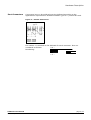
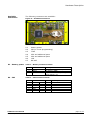
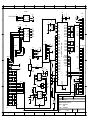
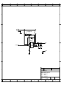
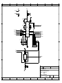
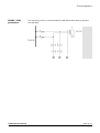
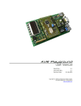
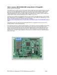
AVRcard
Microcontroller Core Module
User Manual
Board Rev.:
Document Rev.:
Revision Date:
1.1
1.1a
06.01.2004
www.avrcard.com
Product Overview
Contents
Section 1
4
Product Overview
4
Key Features........................................................................ 4
Additional Resources ............................................................. 4
Section 2
5
Getting started
5
Handling Precautions............................................................. 5
System Requirements ........................................................... 5
Quick Start .......................................................................... 5
Section 3
7
Hardware Description
7
Functional Blocks.................................................................. 7
CPU
7
FRAM
7
RTC
7
DC-DC Converter ........................................................ 8
RS-232 Driver ............................................................ 8
RS-485 Driver ............................................................ 8
Interfaces ............................................................................ 8
I2C
8
Serial Communication.................................................. 8
Port Connectors.................................................................... 9
Available Connectors ................................................. 10
X1 - battery power.................................................... 10
X2 - ISP 10
X3 - JTAG 11
X4 - common ports ................................................... 11
X5 - common ports ................................................... 12
X6 - LCD 12
X7 - RS485 .............................................................. 13
Jumpers ............................................................................ 13
J1 - RX/TX select ...................................................... 13
ADC reference voltage......................................................... 14
Section 4
15
Programming
15
Programming ..................................................................... 15
Section 5
AVRcard User Manual
Rev. 1.1a, 06.01.2004
16
page 2/19
www.avrcard.com
Product Overview
Circuit Diagrams
16
Bill of Materials................................................................... 17
RS485 - ESD protection....................................................... 18
Section 6
19
References
19
Data Sheets ....................................................................... 19
Contact ............................................................................. 19
Figures
Figure 1 – Functional Blocks of the AVRcard .......................................... 7
Figure 2 – Header dimensions.............................................................. 9
Figure 3 – Available Connectors ......................................................... 10
Figure 4 – Serial Port Configuration Jumpers ....................................... 13
Figure 5 – Location of ADC Reference Voltage Regulator ....................... 14
Tables
Table 1 – Commands of the preloaded terminal monitor.......................... 6
Table 2 – Battery Connector Pinout .................................................... 10
Table 3 – ISP Connector Pinout .......................................................... 10
Table 4 – JTAG Connector Pinout........................................................ 11
Table 5 – Common Ports Connector Pinout .......................................... 11
Table 6 – Common Ports Connector Pinout .......................................... 12
Table 7 – Standard LCD Connector Pinout ........................................... 12
Table 8 – RS-485 Connector Pinout .................................................... 13
Table 9 – List of Parts ....................................................................... 17
Author:
Hans Kallen
Keywords:
AVRcard, ATmega128, prototyping, RS-485, LCD, FM24C256
This document is originally distributed by AVRcard.com, and may be distributed, reproduced, and modified
without restrictions. Updates and additional design notes can be found at: www.avrcard.com under
“Resources”.
AVRcard User Manual
Rev. 1.1a, 06.01.2004
page 3/19
www.avrcard.com
Product Overview
Section 1
Product Overview
The AVRcard has been designed to enable developers to rapidly prototype AVR based applications.
The board features the most powerful 8-bit RISC CPU to date from Atmel. The board has been
designed by ESS Development AG. It supports rapid development of applications for the
ATmega128 8-bit RISC CPU by providing a multitude of useful hardware features.
Key Features
ATmega128 8-bit RISC CPU
32Kbytes, 2-wire serial ferromagnetic RAM (FM24C256-SE) for
persistent data storage without backup power
2-wire serial real time clock providing additional square wave output 132KHz (DS1307)
3V lithium battery keeping time and date up to 5 years
RS-485 driver for two wire networking up to 1.5 km (MAX485)
RS-232 driver supporting two serial interfaces (MAX202)
Step-up voltage converter for 2-5V battery power supply or long supply
wiring (MAX1674)
all SMD assembly except analog voltage reference and header
connectors which can be soldered manually according to the user’s
requirements
CPU ports routed directly to connectors for unrestricted use (ESD
protected by series resistors)
connector for standard LCD with adjustable negative contrast voltage
output
ISP connector
JTAG connector
5V supply
credit card size (87 x 54mm)
Additional
Resources
Product Information – All updated product information can be
retrieved at the Web Site, www.avrcard.com.
Application Support – Please check the Resources pages regularly at
www.avrcard.com for design notes and application hints. Further
support is available by email from [email protected].
Custom Designs – Custom versions of the product are available. For
inquiries please contact [email protected].
AVRcard User Manual
Rev. 1.1a, 06.01.2004
page 4/19
www.avrcard.com
Getting started
Section 2
Getting started
Handling
Precautions
Most of the CPU ports on the AVRcard are protected by series resistors
against electrostatic discharge. Please note that this is not a 100%
protection and does not apply to all port pins. Always observe ESD
protection standards while working with the board.
Especially the RS-485 transceiver chip is sensitive to electrostatic
discharge. Therefore, an external protection circuit should be considered in
rough environments. Refer to chapter RS485 - ESD protection.
Never use battery power supply and external supply simultainously! The
step up converter can be damaged due to reverse current flow.
System
Requirements
Power Supply: 5VDC +/- 10%
PC with terminal software, 19'200 bit/s, 8 data bits, no parity
Cable for serial communications
Quick Start
Your AVRcard has been factory tested and shipped with the terminal
software loaded. You can test basic functions of the board by using this
preloaded software.
1.
Connect a regulated 5VDC power supply to the AVRcard.
2.
Connect a cable for serial communications between the serial port 1
of the AVRcard and your PC.
Connect these signals to a female 9 pin D-Sub connector which plugs
into the COM port of your PC, as follows:
Pin 2: TXD1
Pin 3: RXD1
Pin 5: GND
AVRcard User Manual
Rev. 1.1a, 06.01.2004
3.
Set jumper RX1 select.
4.
Start your terminal program with the settings 19200 bps, 8 bits, no
parity, 1 stop bit, no flow control.
5.
Switch on the power supply. The AVRcard will report the command
prompt '>'. Now you can send commands according to the table
below. Enter '?'-'Return' to get a help text describing all the available
commands.
page 5/19
www.avrcard.com
Getting started
Table 1 – Commands of the preloaded terminal monitor
Command
AVRcard User Manual
Rev. 1.1a, 06.01.2004
Description
?<cr>
display this help text
help<cr>
display this help text
<ctrl><q>
serial port transparent mode (on/off)
dt<cr>
display current date and time
st<cr>
set date and time
wr<cr>
write hex byte to fram
wrtxt<cr>
write text to fram
rdump<cr>
fram hex dump
sp<cr>
show i/o port
wd<cr>
write i/o port data direction
wp<cr>
write i/o port bit
reg<cr>
read control registers
cf<cr>
create file
df<cr>
delete file
wf<cr>
write text to file
rf<cr>
read file content
fseek<cr>
read file content at specific address
fdump<cr>
file hex dump
dir<cr>
show files on virtual disk
disk<cr>
show free virtual disk space
format<cr>
format virtual disk
vref<cr>
set reference voltage for adc
adc<cr>
read voltages at adc ports
page 6/19
www.avrcard.com
Hardware Description
Section 3
Hardware Description
Functional
Blocks
Figure 1 shows the board and its different functional areas. These areas are
detailed in the following sections.
Figure 1 – Functional Blocks of the AVRcard
CPU
Some of the ATMEGA128 ports are routed to more than one connector or
used internally. See chapter Available Connectors.
FRAM
The FM24C256 is a 256-kilobit nonvolatile memory employing an advanced
ferroelectric process. A ferroelectric random access memory or FRAM is
nonvolatile and performs reads and writes like a RAM. It provides reliable
data retention for 10 years while eliminating the complexities, overhead,
and system level reliability problems caused by EEPROM and other
nonvolatile memories.
The FM24C256 performs write operations at bus speed. No write delays are
incurred. The next bus cycle may commence immediately without the need
for data polling. In addition, the product offers write endurance orders of
magnitude higher than EEPROM. Also, FRAM exhibits much lower power
during writes than EEPROM since write operations do not require an
internally elevated power supply voltage for write circuits.
RTC
AVRcard User Manual
Rev. 1.1a, 06.01.2004
The DS1307 Serial Real-Time Clock is a low-power, full binary-coded
decimal (BCD) clock/calendar plus 56 bytes of NV SRAM. Address and data
are transferred serially via a 2-wire, bi-directional bus. The clock/calendar
provides seconds, minutes, hours, day, date, month,and year information.
The end of the month date is automatically adjusted for months with fewer
page 7/19
www.avrcard.com
Hardware Description
than 31 days, including corrections for leap year. The clock operates in
either the 24-hour or 12-hour format with AM/PM indicator. The DS1307
has a built-in power sense circuit that detects power failures and
automatically switches to the battery supply.
DC-DC Converter
The MAX1674 step-up DC-DC converter features a built-in synchronous
rectifier, which improves efficiency and reduces size and cost by
eliminating the need for an external Schottky diode. Quiescent supply
current is only 16µA. The input voltage ranges from 0.7V to Vout, where
Vout can be set from 2V to 5.5V. Start-up is guaranteed from 1.1V inputs.
The MAX1674 has a preset, pin-selectable output for 5V or 3.3V. On the
AVRcard, the output voltage is preset to 5V by R13, R24 is omitted.
Note: The MAX1674 may not be reversely fed. Therefore, never use battery
power supply and external supply simultainously. The step up converter
can be damaged.
RS-232 Driver
The MAX202E line driver/receiver is designed for RS-232 and V.28
communications in harsh environments. Each transmitter output and
receiver input is protected against ±15kV electrostatic discharge (ESD)
shocks,without latchup. The drivers and receivers meet all EIA/TIA-232E
and CCITT V.28 specifications at data rates up to 120kbps, when loaded in
accordance with the EIA/TIA-232E specification.
RS-485 Driver
The MAX485 is a low-power transceiver for RS-485 communication. Each
part contains one driver and one receiver. The driver slew rates of the
MAX485 is not limited, allowing it to transmit up to 2.5Mbps. These
transceivers draw between 120µA and 500µA of supply current when
unloaded or fully loaded with disabled drivers. The device operates from a
single 5V supply. Drivers are short-circuit current limited and are protected
against excessive power dissipation by thermal shutdown circuitry that
places the driver outputs into a high-impedance state. The receiver input
has a fail-safe feature that guarantees a logic-high output if the input is
open circuit.
Interfaces
I2C
Internal FRAM and RTC use I2C bus on PD0 (SCL) and PD1 (SCA). These
lines are pulled up to VCC by 2K7 resistors. This allows external I2C
devices to be attached directly. The DS1307 limits bus speed to 100kHz.
Serial
Communication
The two serial interfaces of the Atmega128 can be configured in various
ways:
Serial port 1 (PE0, PE1) transmits to TTL and RS-232 simultainously.
Receives from TTL
Serial port 1 receives from RS-232.
Serial port 2 (PD2, PD3) transmits to TTL and simultainously to RS-232
Serial port 2 transmits to TTL and RS-485
Serial port 2 receives from TTL
Serial port 2 receives from RS-232
Serial port 2 receives from RS-485.
Note: Whenever reception from RS-232 or RS-485 is selected no TTL input
signal must be connected to the corresponding pins on the AVRcard as it
would interfer with the signal from transceivers Refer to chapter Jumpers.
AVRcard User Manual
Rev. 1.1a, 06.01.2004
page 8/19
www.avrcard.com
Hardware Description
Port Connectors
Connectors have to be soldered onto the AVRcard according to the
application’s requirements. Standard headers (grid 0.1") should be used.
Figure 2 – Header dimensions
Pin number 1 is marked on the AVRcard for each connector. Pins are
numbered as follows:
2 4 ...
Numbering:
1 3 ...
AVRcard User Manual
Rev. 1.1a, 06.01.2004
1 2 3 ...
page 9/19
www.avrcard.com
Hardware Description
Available
Connectors
The following connectors are available:
Figure 3 – Available Connectors
X1:
X1 - battery power
battery power
X2:
ISP (in circuit programming)
X3:
JTAG
X4:
CPU and additional ports
X5:
CPU and additional ports
X6:
LCD
X7:
RS-485
Table 2 – Battery Connector Pinout
Pin
1
2
3
X2 - ISP
Description
BATT+
BATT/LOWBATT
+2..5V battery power input
0V battery (GND)
is pulled low if battery voltage
drops below 1.3V
Table 3 – ISP Connector Pinout
Pin
1
2
3
4
5
6
AVRcard User Manual
Rev. 1.1a, 06.01.2004
Function
Function
I/O
PE1
VCC
PB1
PE0
RST
GND
i/o
pwr
i/o
i/o
i
pwr
TXD
SCK
RXD
Description
page 10/19
www.avrcard.com
Hardware Description
X3 - JTAG
Table 4 – JTAG Connector Pinout
Pin
1
2
3
4
5
6
7
8
9
10
X4 - common ports
Function
I/O
PF5
VCC
PF4
PF7
RST
GND
PF6
-
i/o
pwr
i/o
i/o
i
pwr
-
Description
not connected
not connected
not connected
Please note that the ports on the connector are not always numbered in
the same direction.
Table 5 – Common Ports Connector Pinout
AVRcard User Manual
Rev. 1.1a, 06.01.2004
Pin
Function
I/O
1
2
3
4
5
6
7
8
9
10
11
12
13
14
15
16
17
18
19
20
21
22
23
24
25
26
27
28
29
30
31
32
PC0
PC1
PC2
PC3
PC4
PC5
PC6
PC7
PA7
PA6
PA5
PA4
PA3
PA2
PA1
PA0
ALE
/RD
/WR
SQW
VCC
VCC
GND
GND
PF7
PF6
PF5
PF4
PF3
PF2
PF1
PF0
i/o
i/o
i/o
i/o
i/o
i/o
i/o
i/o
i/o
i/o
i/o
i/o
i/o
i/o
i/o
i/o
o
o
o
o
pwr
pwr
pwr
pwr
i/o
i/o
i/o
i/o
i/o
i/o
i/o
i/o
A8
A9
A10
A11
A12
A13
A14
A15
AD7
AD6
AD5
AD4
AD3
AD2
AD1
AD0
ADC7
ADC6
ADC5
ADC4
ADC3
ADC2
ADC1
ADC0
ESD
Internal Connections
X6/11
X6/12
X6/13
X6/14
X6/6
X6/4
X6/5
data direction select for RS-485
page 11/19
www.avrcard.com
Hardware Description
X5 - common ports
X6 - LCD
AVRcard User Manual
Rev. 1.1a, 06.01.2004
Table 6 – Common Ports Connector Pinout
Pin
Function
I/O
1
2
3
4
5
6
7
8
9
10
11
12
13
14
15
16
17
18
19
20
21
22
23
24
25
26
27
28
29
30
31
32
PE0
PE1
PE2
PE3
PE4
PE5
PE6
PE7
PB0
PB1
PB2
PB3
PB4
PB5
PB6
PB7
PD0
PD1
PD2
PD3
PD4
PD5
PD6
PD7
VCC
VCC
GND
GND
RX1
RX2
TX1
TX2
i/o
i/o
i/o
i/o
i/o
i/o
i/o
i/o
i/o
i/o
i/o
i/o
i/o
i/o
i/o
i/o
i/o
i/o
i/o
i/o
i/o
i/o
i/o
i/o
pwr
pwr
pwr
pwr
i
i
o
o
RXD
TXD
AC+
ACINT4
INT5
INT6
INT7
SS
SCK
MOSI
MISO
OC0
OC1A
OC1B
OC2
INT0
INT1
INT2
INT3
IC1
T1
T2
VCC
VCC
GND
GND
ESD
Internal Connections
SCL on FRAM and RTC
SDA on FRAM and RTC
Table 7 – Standard LCD Connector Pinout
Pin
Function
I/O
ESD
Internal Connection
1
2
3
4
5
6
7
8
9
10
11
12
13
14
GND
VCC
V0
PC5
PC6
PC4
PC0
PC1
PC2
PC3
pwr
pwr
pwr
i/o
i/o
i/o
X4/6
X4/7
X4/5
i/o
i/o
i/o
i/o
X4/1
X4/2
X4/3
X4/4
page 12/19
www.avrcard.com
Hardware Description
X7 - RS485
Table 8 – RS-485 Connector Pinout
Jumpers
Pin
Function
I/O
ESD prot
1
2
3
4
GND
B
A
-
-
no
no
no
no
Description
120Ω bus termination
resistor. Bus can be
terminated by placing a
bridge on external
connector (pin4 to pin 2)
at far end node.
Jumpers are installed on the AVRcard to select the different possible
combinations of serial transmission and reception supplied by the two
UARTs on the ATmega128. RS-232, RS-485 and serial port with TTL level
can be selected.
Jumpers are standard (0.1").
Figure 4 – Serial Port Configuration Jumpers
RX2 select
RX1 select
TX2 select
1
RS232 RS485
Serial port 1 can be configured for
RS-232 only. For serial port 2, RS232 or RS-485 can be selected.
J1 - RX/TX select
RX1 select:
In transmit direction the TTL signal is routed from the ATMEGA128 to the
RS232 transceiver (X5/pin31 [TX1]) as well as to the TTL port (X5/pin2
[PE1]). So that the receive direction signal from the RS232 transceiver
(X5/pin29 [RX1]) does not interfere with the TTL port signal (X5/pin1
[PE0]), this jumper should be set accordingly.
AVRcard User Manual
Rev. 1.1a, 06.01.2004
jumper on:
RS232 RX
jumper off:
TTL RX
1
page 13/19
www.avrcard.com
Hardware Description
RX2 select:
In receive direction the serial port 2 can accept it's signal from TTL
(X5/pin19 [PD2]), RS232 (X5/pin30 [RX2]) or RS485 (X7) inputs.
jumper off:
1
RS232 RX
1
RS485 RX
TTL RX
jumper left:
RS232 RX
jumper right:
RS485 RX
TX2 select:
In transmit direction the serial port 2 can be connected to TTL (X5/pin10
[PD3]), RS232 (X5/pin32 [TX2]) or RS485 (X7) outputs.
ADC reference
voltage
jumper off:
TTL TX only
jumper left:
RS232 and TTL TX
jumper right:
RS485 and TTL TX
1
RS232 and TTL TX
1
RS485 and TTL TX
The ATMEGA128 provides several internal analog to digital converters.
Whenever you want to use a more precise or a different reference voltage
(i.e. LM4040AIM) than the internal one you can solder this element
manually as needed. The footprint of U2 fits to a TO-92 case.
Figure 5 – Location of ADC Reference Voltage Regulator
LM4040 orientation (top
view)
AVRcard User Manual
Rev. 1.1a, 06.01.2004
page 14/19
www.avrcard.com
Programming
Section 4
Programming
Programming
For programming you can use the ISP connecter as well as the JTAG
connector. It is advised to refer to datasheets of ATmega128 and your
programmer as well as this document for the exact connection method. Pin
allocation matches ATMEL starter kit programmer as well as ISP/JTAG
programmers manufactured by e-Lab (www.e-Lab.de).
Never use battery power supply while programming !
The step up convertor can be damaged due reverse current flow as VCC is
also provided on programming connectors.
AVRcard User Manual
Rev. 1.1a, 06.01.2004
page 15/19
www.avrcard.com
Circuit Diagrams
Section 5
Circuit Diagrams
These diagrams are also availabe as a separate document.
Main circuit
Power
Communication
Parts Placement
AVRcard User Manual
Rev. 1.1a, 06.01.2004
page 16/19
www.avrcard.com
3
2
C14
ISP
R10
VCC
VCC
1
2
3
4
5
6
PE1
PB1
PE0
HDR_6
GND
PF4
PF7
PF6
HDR_10
3
R6
3V VCC
GND
SDA
SCL
SQW
GND
X1
X2
VBAT
VCC
36 DS1307
5
6
7
4
GND
VCC
PD0
SQW
6
5
21
VCC
52
VCC
A8-PC0
A9-PC1
A10-PC2
A11-PC3
A12-PC4
A13-PC5
A14-PC6
A15-PC7
R18
35
36
37
38
39
40
41
42
1
3
5
7
1
3
5
7
R20
GND
4
1
3
5
7
1
3
5
7
47
R19
47
HDR_14
2
4
6
8
2
4
6
8
47
R21
47
PC0
DDR
OC2-PB7
OC1B-PB6
OC1A-PB5
OC0-PB4
MISO-PB3
MOSI-PB2
SCK-PB1
SS-PB0
17
16
15
14
13
12
11
10
PC7
PA7
PA0
ALE
RD
WR
PEN
AVCC
43
34
33
1
SQW
AVREF
VCC
AGND
D
PF7
1
3
5
7
1
3
5
7
R22
47
R23
47
2
4
6
8
2
4
6
8
X4
1
2
3
4
5
6
7
8
9
10
11
12
13
14
15
16
17
18
19
20
21
22
23
24
25
26
27
28
29
30
31
32
HDR_32
C
B
PF0
GND
7
63
ADC0-PF0
ADC1-PF1
ADC2-PF2
ADC3-PF3
ADC4-PF4
ADC5-PF5
ADC6-PF6
ADC7-PF7
R9
X5
8
62
PD0-INT0
PD1-INT1
PD2-INT2
PD3-INT3
PD4-IC1
PD5
PD6-T1
PD7-T2
24
+
2k7
PD1
64
RXD-PE0
TXD-PE1
AC+_PE2
AC-_PE3
INT4-PE4
INT5-PE5
INT6-PE6
INT7-PE7
2
4
6
8
2
4
6
8
1k0
1
2
3
8
0.1uF
C12
0.1uF
2k7
VCC
GND
33
PE0
C11
R8 R7
2
PB7
PB0
PE7
VCC
WP
SCL
SDA
47uH
8
7
6
5
21 FM24C256
XTAL2
47
2
4
6
8
AO
A1
A2
VSS
GND
U2
47
R12
1
2
3
4
0.1uF
R17
2
4
6
8
2
4
6
8
1
3
5
7
61
60
59
58
57
56
55
54
L1
C13
47
PD0
32.768K
R16
17
MCP809
GND
1
47
4k7
+
R15
PD7
-
47
2
4
6
8
2
4
6
8
1
VCC
2
1
3
5
7
1
3
5
7
R14
+
GND
1
3
5
7
1
3
5
7
25
26
27
28
29
30
31
32
VCC
RES
VCC
32
31
30
29
28
27
26
25
24
23
22
21
20
19
18
17
16
15
14
13
12
11
10
9
8
7
6
5
4
3
2
1
A
1
2
3
4
HDR_4
HDR_32
B
X2
PF5
TOSC1
TOSC2
51
50
49
48
47
46
45
44
GND
GND
X7
120
C
1
2
3
4
5
6
7
8
9
10
JTAG
2
3
4
5
6
7
8
9
AD0-PA0
AD1-PA1
AD2-PA2
AD3-PA3
AD4-PA4
AD5-PA5
AD6-PA6
AD7-PA7
X6
1
2
3
PC5 4
5
6
PC6
7
PC4
8
9
10
PC0
11
PC1
12
PC2
13
PC3
14
VCC
GND
X3
RS-485
19
18
XTAL1
XTAL2
ATMEGA128
V0
DDR
PD3
PE1
PD2
PE0
LCD
V0
QFP64
V0 14
13
DDR
12
T1_IN
11
T2_IN
10
R1_OUT
9
R2_OUT
RESET
53
22
VCC
GND
T1_OUT
T2_OUT
R1_IN
R2_IN
A
B
24
23
LM4040AIM
1
2
3
4
5
6
7
8
16M
COM
-
VCC
GND
20
XTAL1
GND
12pF
HDR_3
12pF
6
5
VCC
GND
VCC
BATT+
BATT/LOWBATT
C5
D
VCC
VCC
C6
BATTERY POWER
1
2
3
GND
1
2
3
GND
POWER
X1
1
VCC
4
GND
5
GND
6
0.1uF
7
GND
8
REV: 1.1A
DATE:
PROJECT:
AVR_CARD
COMPANY:
ADDRESS:
CITY
COUNTRY:
ESS DEVELOPMENT AG
WWW.ESS.CH
WORB
SWITZERLAND
INITIAL
3
06.01.2004
ENG: HK
A
8.11.2002
PAGE:
2
1
OF:
3
1
8
7
6
5
4
3
2
1
D
D
BATT+
L2
BATT-
C
22uH
0
100K
R11
0
R24
R13
GND
GND
C
3.3 / 5V SELECTION
MAX1674
/LOWBATT
FB
OUT
LBI
LX
LBO GND
REF SHDN
8
7
6
5
GND
1
2
3
4
62
+
VCC
C18
0.1uF GND
C15
B
C16
47uF
GND
GND
0.1uF
A
REV: 1.1
DATE:
PROJECT:
AVR_CARD
COMPANY:
ADDRESS:
CITY
COUNTRY:
ESS DEVELOPMENT AG
WWW.ESS.CH
WORB
SWITZERLAND
INITIAL
8
7
6
5
B
GND
GND
4
3
17.01.2003
ENG: SK
A
8.11.2002
PAGE:
2
3
OF:
3
1
7
6
5
VCC
4
2
1
VCC
C19
0.1uF
VCC
GND
D
GND
D
GND
0.1uF
16
0.1uF
C1
2 V+ VCC
1
0.1uF
T1_OUT
120
T2_OUT
120
R1_IN
120
R2_IN
120
3
R4 R5 R2 R3
C2
C
3
GND
8
C4
V-6
C1+
C1-
C2+
U1
MAX202
R1
0.1uF
V0
10k
C2-
5
C3
VCC
11
T1_IN
10
T2_IN
14
T1_OUT
7
T2_OUT
13
R1_IN
8
R2_IN
4
T2_IN
C
T1_IN
12
R1_OUT
9
R2_OUT
R2_OUT
R1_OUT
15
GND
1
2
3
4
5
6
7
8
0.1nF 0.1nF 0.1nF 0.1nF
C9
C10
HDR_8
C8
J8
C7
GND
B
GND
RX/TX SELECTOR
B
A
A
GND
DI
DE
55
B
VCC
RO
RE
DDR
GND
0.1uF
C17
1
2
3
4
MAX485
8
7
6
5
B
A
VCC
REV: 1.1
DATE:
PROJECT:
AVR_CARD
COMPANY:
ADDRESS:
CITY
COUNTRY:
ESS DEVELOPMENT AG
WWW.ESS.CH
WORB
SWITZERLAND
INITIAL
8
7
6
5
4
3
17.01.2003
ENG: SK
A
8.11.2002
PAGE:
2
2
OF:
3
1
Circuit Diagrams
Bill of Materials
Table 9 – List of Parts
Qty.
AVRcard User Manual
Rev. 1.1a, 06.01.2004
DEVICE
VALUE
1
1
1
1
1
1
1
1
1
1
1
1
1
1
1
1
1
1
1
1
1
1
1
1
11
ATMEGA128
BATT
COIL
COIL
DS1307
ELCO
FM24C256
HDR_10
HDR_14
HDR_3
HDR_4
HDR_6
HDR_8
LM4040AIM
MAX1674
MAX202
MAX485
MCP809
POT_METER
RESISTOR
RESISTOR
RESISTOR
XTAL
XTAL
RARRAY
12
CAPACITOR
0.1uF
2
2
2
2
4
5
CAPACITOR
HDR_32
RESISTOR
RESISTOR
CAPACITOR
RESISTOR
12pF
3V
22uH
47uH
47uF
-
10k
100K
1k0
4k7
16M
32.768KHz
47
0
2k7
0.1nF
120
Refdes
24
33
L2
L1
36
C18
21
X3
X6
X1
X7
X2
J8
U2
62
U1
55
17
R1
R11
R9
R6
XTAL1
XTAL2
R14,R15,R16,R17,R18,R19,
R20,R21,R22,R12,R23
C12,C2,C13,C3,C14,C4,C15
,C16,C17,C19,C11,C1
C5,C6
X4, X5
13,R24
R7,R8
C7,C8,C9,C10
R2,R3,R4,R5,R10
page 17/19
www.avrcard.com
Circuit Diagrams
RS485 - ESD
protection
AVRcard User Manual
Rev. 1.1a, 06.01.2004
The following circuit is recommended for RS-485 busses that go beyond
the lab desk.
page 18/19
www.avrcard.com
References
Section 6
References
Data Sheets
Contact
ATMEGA128:
www.atmel.com
FM24C256-SE:
www.ramtron.com
DS1307, MAX202, MAX485, MAX1674:
www.maxim-ic.com
Elektronik-Atelier
Hans Kallen
Steinackerweg 14
CH-3075 Rüfenacht
Switzerland
www.avrcard.com
[email protected]
Phone: +41 31 832 1441
Fax:
AVRcard User Manual
Rev. 1.1a, 06.01.2004
+41 31 832 1442
page 19/19
www.avrcard.com