1
FXCPU
Structured Programming Manual
Device & Common
FXCPU Structured Programming Manual
[Device & Common]
FXCPU Structured Programming Manual
[Device & Common]
Manual No.
JY997D26001
Revision
L
Date
4/2015
Foreword
This manual describes devices and parameters for structured programs used in the MELSEC-F FX Series.
Please read this manual and manuals of relevant products before use, sufficiently understand the
specifications, and use the unit correctly and safely.
See to it that this manual is supplied to the end user.
This manual confers no industrial property rights or any rights of any other kind, nor does it confer any patent licenses.
Mitsubishi Electric Corporation cannot be held responsible for any problems involving industrial property rights which may occur as a
result of using the contents described in this manual.
© 2009 Mitsubishi Electric Corporation
1
FXCPU Structured Programming Manual
[Device & Common]
Outline Precautions
• This manual provides information for the use of the FX Series Programmable Controllers. The manual has
been written to be used by trained and competent personnel. The definition of such a person or persons is
as follows;
a) Any engineer who is responsible for the planning, design and construction of automatic equipment
using the product associated with this manual should be of a competent nature, trained and qualified
to the local and national standards required to fulfill that role. These engineers should be fully aware
of all aspects of safety with regards to automated equipment.
b) Any commissioning or service engineer must be of a competent nature, trained and qualified to the
local and national standards required to fulfill that job. These engineers should also be trained in the
use and maintenance of the completed product. This includes being completely familiar with all
associated documentation for the said product. All maintenance should be carried out in accordance
with established safety practices.
c) All operators of the completed equipment should be trained to use that product in a safe and
coordinated manner in compliance to established safety practices. The operators should also be
familiar with documentation which is connected with the actual operation of the completed
equipment.
Note: the term 'completed equipment' refers to a third party constructed device which contains or uses
the product associated with this manual
• This product has been manufactured as a general-purpose part for general industries, and has not been
designed or manufactured to be incorporated in a device or system used in purposes related to human life.
• Before using the product for special purposes such as nuclear power, electric power, aerospace, medicine
or passenger movement vehicles, consult with Mitsubishi Electric.
• This product has been manufactured under strict quality control. However when installing the product
where major accidents or losses could occur if the product fails, install appropriate backup or failsafe
functions in the system.
• When combining this product with other products, please confirm the standard and the code, or regulations
with which the user should follow. Moreover, please confirm the compatibility of this product to the system,
machine, and apparatus with which a user is using.
• If in doubt at any stage during the installation of the product, always consult a professional electrical
engineer who is qualified and trained to the local and national standards. If in doubt about the operation or
use, please consult the nearest Mitsubishi Electric representative
• Since the examples indicated by this manual, technical bulletin, catalog, etc. are used as a reference,
please use it after confirming the function and safety of the equipment and system. Mitsubishi Electric will
accept no responsibility for actual use of the product based on these illustrative examples.
• This manual content, specification etc. may be changed without a notice for improvement.
• The information in this manual has been carefully checked and is believed to be accurate; however, you
have noticed a doubtful point, a doubtful error, etc., please contact the nearest Mitsubishi Electric
representative.
Registration
• Microsoft®, Windows® and Excel® are either registered trademarks or trademarks of Microsoft Corporation
in the United States and/or other countries.
• CompactFlash is a trademark of SanDisk Corporation in the United States and other countries.
• Ethernet is a trademark of Xerox Corporation.
• MODBUS® is a registered trademark of Schneider Electric SA.
• The company name and the product name to be described in this manual are the registered trademarks or
trademarks of each company.
2
FXCPU Structured Programming Manual
[Device & Common]
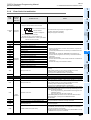
Table of Contents
Table of Contents
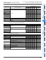
Positioning of This Manual....................................................................................................... 6
Related Manuals ........................................................................................................................ 9
Generic Names and Abbreviations Used in Manuals .......................................................... 12
1. Device Outline
13
1.1 Devices Constructing PLC ......................................................................................................... 13
1.1.1 Relation among devices ................................................................................................................ 14
1.1.2 Device function list......................................................................................................................... 15
1.2 Program Memory and Devices................................................................................................... 17
1.2.1
1.2.2
1.2.3
1.2.4
1.2.5
Memory structure........................................................................................................................... 17
Memory operations and backup against power interruption (power ON/OFF and RUN/STOP) ... 22
Types of backup methods against power interruption ................................................................... 32
Change of devices between general type and latched (backed-up) type...................................... 33
How to initialize latched (backed-up) type devices........................................................................ 33
2. Devices in Detail
35
2.1 Device Number List..................................................................................................................... 35
2.2 Input/Output Relays [X and Y] ................................................................................................... 37
2.2.1 Numbers of input/output relays...................................................................................................... 37
2.2.2 Functions and roles ....................................................................................................................... 39
2.2.3 Operation timing of I/O relays........................................................................................................ 40
2.3 Auxiliary relay [M] ....................................................................................................................... 41
2.3.1 Numbers of auxiliary relays ........................................................................................................... 41
2.3.2 Functions and operation examples................................................................................................ 42
2.4 State Relay [S] ............................................................................................................................. 44
2.4.1 Numbers of state relays................................................................................................................. 44
2.4.2 Functions and operation examples................................................................................................ 46
2.5 Timer [T]....................................................................................................................................... 48
2.5.1
2.5.2
2.5.3
2.5.4
2.5.5
2.5.6
2.5.7
Numbers of timers ......................................................................................................................... 48
Functions and operation examples................................................................................................ 50
Set value specification method...................................................................................................... 52
Cautions on use............................................................................................................................. 52
Details of timer operations and timer accuracy ............................................................................. 52
Program examples [Off-delay timer and flicker timer] ................................................................... 53
Handling timers as numeric devices.............................................................................................. 54
2.6 Counter [C] .................................................................................................................................. 55
2.6.1
2.6.2
2.6.3
2.6.4
2.6.5
2.6.6
2.6.7
2.6.8
Numbers of counters ..................................................................................................................... 55
Features of counters...................................................................................................................... 56
Related devices (to specify counting direction) [32-bit counter] .................................................... 56
Functions and operation examples................................................................................................ 57
Set value specification method...................................................................................................... 58
Cautions on use............................................................................................................................. 59
Response speed of counters......................................................................................................... 59
Counters handled as numeric devices .......................................................................................... 59
2.7 High Speed Counter [C].............................................................................................................. 62
2.7.1 Types and device numbers of high speed counters ...................................................................... 62
2.7.2 Input assignment for high speed counters..................................................................................... 69
2.7.3 Handling of high speed counters ................................................................................................... 74
2.7.4 Current value update timing and comparison of current value ...................................................... 77
2.7.5 Related devices ............................................................................................................................. 78
2.7.6 Change of logic of external reset input signal................................................................................ 79
2.7.7 Assignment of counter input terminal and switching of function.................................................... 80
2.7.8 How to use 2-phase 2-counting input counters C251 to C255 for 4-edge counting ...................... 82
2.7.9 Condition under which hardware counters are handled as software counters .............................. 83
2.7.10 Response frequency of high speed counters .............................................................................. 84
2.7.11 Cautions on use........................................................................................................................... 92
3
FXCPU Structured Programming Manual
[Device & Common]
Table of Contents
2.8 Data Register and File Register [D] ........................................................................................... 94
2.8.1
2.8.2
2.8.3
2.8.4
2.8.5
Numbers of data registers and file registers.................................................................................. 94
Structure of data registers and file registers.................................................................................. 96
Functions and operation examples of data registers..................................................................... 96
Functions and operation examples of file registers ....................................................................... 99
Cautions on using file registers ................................................................................................... 103
2.9 Extension Register [R] and Extension File Register [ER] ..................................................... 104
2.9.1
2.9.2
2.9.3
2.9.4
2.9.5
2.9.6
2.9.7
2.9.8
Numbers of extension registers and extension file registers ....................................................... 104
Data storage destination and access method ............................................................................. 104
Structure of extension registers and extension file registers ....................................................... 105
Initialization of extension registers and extension file registers................................................... 105
Functions and operation examples of extension registers .......................................................... 106
Functions and operation examples of extension file registers..................................................... 107
Cautions on using extension file registers ................................................................................... 109
Registration of data stored in extension registers and extension file registers............................ 111
2.10 Index Register [V and Z] ......................................................................................................... 115
2.10.1 Numbers of index registers........................................................................................................ 115
2.10.2 Functions and structures ........................................................................................................... 116
2.10.3 Indexing of devices.................................................................................................................... 116
2.11 Pointer [P and I]....................................................................................................................... 117
2.11.1 Numbers of pointers .................................................................................................................. 117
2.11.2 Functions and operation examples of branch pointers.............................................................. 118
2.11.3 Functions and operation examples of interrupt pointers............................................................ 119
3. How to Specify Devices and Constants in Instructions
124
3.1 Numeric Values Handled in PLCs (Octal, Decimal, Hexadecimal and Real Numbers)....... 124
3.1.1 Types of numeric values.............................................................................................................. 124
3.1.2 Conversion of numeric values ..................................................................................................... 125
3.1.3 Handling of numeric values in floating point operations .............................................................. 125
3.2 Specification of Constants K, H and E (Decimal, Hexadecimal and Real Numbers) .......... 128
3.2.1 Constant "K" (decimal number) ................................................................................................... 128
3.2.2 Constant "H" (hexadecimal number) ........................................................................................... 128
3.2.3 Constant "E" (real number).......................................................................................................... 128
3.3 Character Strings ...................................................................................................................... 129
3.3.1 Character string constant ("ABC") ............................................................................................... 129
3.3.2 Character string data ................................................................................................................... 129
3.4
3.5
3.6
3.7
Specification of Digits for Bit Devices (Kn***) ..................................................................... 131
Specification of Bit for Word Device [D.b] ........................................................................... 132
Direct Specification of Buffer Memory (U\G) ..................................................................... 132
Indexing ..................................................................................................................................... 133
3.7.1 Indexing in basic instructions....................................................................................................... 133
3.7.2 Indexing in instructions ................................................................................................................ 134
3.7.3 Indexing example for instructions whose number of times of use is restricted............................ 137
4. Operations of Special Devices (M8000 and later, D8000 and later)
138
4.1 Special Device List (M8000 and later, D8000 and later)......................................................... 138
4.1.1 Special auxiliary relays (M8000 and later)................................................................................... 138
4.1.2 Special data registers (D8000 and later) ..................................................................................... 177
4.2 Supplement of Special Devices (M8000 and later and D8000 and later).............................. 216
4.2.1
4.2.2
4.2.3
4.2.4
4.2.5
4.2.6
4.2.7
4.2.8
4.2.9
4
RUN monitor and initial pulse [M8000 to M8003] ........................................................................ 216
Watchdog timer time [D8000] ...................................................................................................... 217
Low battery voltage detection [M8005 and M8006]..................................................................... 217
Power interruption detection time [D8008, M8008 and M8007] .................................................. 218
Operation cycle (scan time) monitor [D8010 to D8012]............................................................... 219
Internal clock [M8011 to M8014] ................................................................................................. 219
Real-time clock [M8015 to M8019 and D8013 to D8019]............................................................ 220
How to set real-time clock ........................................................................................................... 221
Input filter adjustment [D8020]([D8021])...................................................................................... 223
FXCPU Structured Programming Manual
[Device & Common]
4.2.10
4.2.11
4.2.12
4.2.13
4.2.14
4.2.15
4.2.16
4.2.17
4.2.18
4.2.19
Table of Contents
Battery [BATT (BAT)] LED OFF command [M8030].................................................................. 228
Built-in analog variable potentiometers [D8030, D8031, D8013]............................................... 230
Clear command [M8031 and M8032] ........................................................................................ 231
Memory hold stop [M8033] (Output holding in STOP mode)..................................................... 231
All output disable command [M8034] ........................................................................................ 231
Independent operation for RUN/STOP input [M8035 to M8037] ............................................... 232
Constant scan mode [M8039 and D8039] (Fixed scan time) .................................................... 233
State control in program by STL instruction [M8040] ................................................................ 233
Analog expansion boards [M8260 to M8279 and D8260 to D8279].......................................... 234
Analog special adapters [M8260 to M8299 and D8260 to D8299]
(FX3S/FX3G/FX3GC/FX3U/FX3UC PLCs) .................................................................................. 236
5. Errors
243
5.1 FX3S/FX3G/FX3GC/FX3U/FX3UC PLCs...................................................................................... 243
5.1.1 Error detection devices................................................................................................................ 243
5.1.2 Error Code List and Action .......................................................................................................... 245
5.2 FX1S/FX1N/FX1NC/FX2N/FX2NC PLCs ...................................................................................... 254
5.2.1 Error detection devices................................................................................................................ 254
5.2.2 Error Code List and Action .......................................................................................................... 256
5.3 FX0S/FX0/FX0N/FXU/FX2C PLCs............................................................................................... 263
5.3.1 Error detection devices................................................................................................................ 263
5.3.2 Error Code List and Action .......................................................................................................... 265
6. Types and Setting of Parameters
6.1
6.2
6.3
6.4
6.5
269
Parameter List ........................................................................................................................... 270
Parameter Initial Values............................................................................................................ 273
Memory Capacity Setting Range ............................................................................................. 275
Compatible Optional Memory Models..................................................................................... 277
Keyword ..................................................................................................................................... 279
6.5.1 PLC applicability and access restriction ...................................................................................... 279
6.5.2 Registering and changing keywords............................................................................................ 281
6.6 Parameter setting by GX Works2 ............................................................................................ 284
6.6.1 PLC Parameter setting ................................................................................................................ 284
6.6.2 Network parameter ...................................................................................................................... 298
6.6.3 Transferring parameters (, sequence program and symbolic information*1) to the PLC ............. 302
7. Other Functions
303
7.1 Symbolic information storage and block password.............................................................. 303
7.1.1 Storage of symbolic information .................................................................................................. 303
7.1.2 Block password ........................................................................................................................... 303
Warranty................................................................................................................................. 305
Revision History .................................................................................................................... 306
5
FXCPU Structured Programming Manual
[Device & Common]
Positioning of This Manual
Positioning of This Manual
This manual explains devices and parameters for structured programs provided by GX Works2. Refer to
other manuals for sequence instructions and application functions.
Refer to each corresponding manual for analog, communication, positioning control and special units and
blocks.
1. When using FX3S/FX3G/FX3GC/FX3U/FX3UC PLCs
MELSEC-Q/L/F Structured Programming Manual (Fundamentals) (Additional Manual)
Q/L/F
This manual explains programming methods, specifications, functions, etc. required to create
structured programs.
Structured
(This manual)
FXCPU Structured Programming Manual [Device & Common] (Additional Manual)
FX
This manual explains devices and parameters for structured programs provided
by GX Works2.
Structured
FXCPU Structured Programming Manual [Basic & Applied Instruction]
FX
Structured
FX
Structured
FX3S
FX3G
FX3GC
FX3U
FX3UC
(Additional Manual)
This manual explains sequence instructions for structured programs provided
by GX Works2.
FXCPU Structured Programming Manual [Application Functions]
(Additional Manual)
This manual explains application functions for structured programs provided
by GX Works2.
FX3S/FX3G/FX3GC/FX3U/FX3UC User's Manual- Analog Control Edition
(Additional Manual)
This manual explains details of analog special function blocks and analog special
adapters for FX3S/FX3G/FX3GC/FX3U/FX3UC PLCs and PID instruction.
Explanation of instructions and instructions used in program examples are expressed
for GX Developer.
FX Series User's Manual -Data Communication Edition (Additional Manual)
FX
FX3S
FX3G
FX3GC
FX3U
FX3UC
Special
unit/block
This manual explains details of simple N:N link, parallel link, computer link, no-protocol
communication (RS and RS2 instructions), programming communication and inverter
communication for FX PLCs.
Explanation of instructions and instructions used in program examples are expressed
for GX Developer.
FX3S/FX3G/FX3GC/FX3U/FX3UC Series User's Manual -Positioning Edition
(Additional Manual)
This manual explains details of wiring, instructions and operations of the positioning
function built in FX3S/FX3G/FX3GC/FX3U/FX3UC PLC main units.
Explanation of instructions and instructions used in program examples are expressed
for GX Developer.
Individual manuals (Manual supplied with product or additional Manual *1)
This manual explains details of each special unit/block.
Explanation of instructions and instructions used in program examples are expressed
for GX Developer.
*1. Detailed explanation may be provided by a separate manual in some products.
6
FXCPU Structured Programming Manual
[Device & Common]
Positioning of This Manual
2. When using FX1S/FX1N/FX1NC/FX2N/FX2NC PLCs
MELSEC-Q/L/F Structured Programming Manual [Fundamentals] (Additional Manual)
Q/L/F
This manual explains programming methods, specifications, functions, etc. required to create
structured programs.
Structured
(This manual)
FXCPU Structured Programming Manual [Device & Common] (Additional Manual)
FX
This manual explains devices and parameters for structured programs provided
by GX Works2.
Structured
FX
FXCPU Structured Programming Manual [Basic & Applied Instruction]
(Additional Manual)
This manual explains sequence instructions for structured programs provided
by GX Works2.
Structured
FX
FXCPU Structured Programming Manual [Application Functions]
(Additional Manual)
This manual explains application functions for structured programs provided
by GX Works2.
Structured
FX Series User's Manual -Data Communication Edition (Additional Manual)
FX
This manual explains details of simple N:N link, parallel link, computer link, no-protocol
communication (RS instruction), programming communication and inverter communication
for FX PLCs.
Explanation of instructions and instructions used in program examples are expressed for
GX Developer and FX-PCS/WIN.
Individual manuals (Manual supplied with product or additional Manual *1 )
Special
unit/block
This manual explains details of each special unit/block.
Explanation of instructions and instructions used in program examples are expressed
for GX Developer and FX-PCS/WIN.
*1. Detailed explanation may be provided by a separate manual in some products.
7
FXCPU Structured Programming Manual
[Device & Common]
Positioning of This Manual
3. When using FX0S/X0/FX0N/FXU/FX2C PLCs
MELSEC-Q/L/F Structured Programming Manual (Fundamentals) (Additional Manual)
Q/L/F
This manual explains programming methods, specifications, functions, etc. required to create
structured programs.
Structured
(This manual)
FXCPU Structured Programming Manual [Device & Common] (Additional Manual)
FX
This manual explains devices and parameters for structured programs provided
by GX Works2.
Structured
FX
FXCPU Structured Programming Manual [Basic & Applied Instruction]
(Additional Manual)
This manual explains sequence instructions for structured programs provided
by GX Works2.
Structured
FX
Structured
FXCPU Structured Programming Manual [Application Functions]
(Additional Manual)
This manual explains application functions for structured programs provided
by GX Works2.
FX Series User's Manual -Data Communication Edition (Additional Manual)
FX
This manual explains details of parallel link, computer link, no-protocol communication
(RS instruction) and programming communication for FX PLCs.
Explanation of instructions and instructions used in program examples are expressed for
GX Developer and FX-PCS/WIN.
Individual manuals (Manual supplied with product or additional Manual *1)
Special
unit/block
This manual explains details of each special unit/block.
Explanation of instructions and instructions used in program examples are expressed
for GX Developer and FX-PCS/WIN.
*1. Detailed explanation may be provided by a separate manual in some products.
8
FXCPU Structured Programming Manual
[Device & Common]
Related Manuals
Related Manuals
This manual explains devices and parameters for structured programs provided by GX Works2.
Refer to other manuals for sequence instructions and applied functions.
This chapter introduces only reference manuals for this manual and manuals which describe the hardware
information of PLC main units.
Manuals not introduced here may be required in some applications.
Refer to the manual of the used PLC main unit and manuals supplied together with used products.
Contact the representative for acquiring required manuals.
Common among FX PLCs [structured]
Manual name
Manual number
Supplied with product
or Additional Manual
Contents
Model
name code
MELSEC-Q/L/F Structured
Programming Manual (Fundamentals)
SH-080782
Additional Manual
Programming methods, specifications, functions,
etc. required to create structured programs
13JW06
FXCPU Structured Programming
Manual [Device & Common]
JY997D26001
Additional Manual
Devices, parameters, etc. provided in structured
projects of GX Works2
09R925
FXCPU Structured Programming
Manual [Basic & Applied Instruction]
JY997D34701
Additional Manual
Sequence instructions provided in structured
projects of GX Works2
09R926
FXCPU Structured Programming
Manual [Application Functions]
JY997D34801
Additional Manual
Application functions provided in structured
projects of GX Works2
09R927
FX3S/FX3G/FX3GC/FX3U/FX3UC PLCs
Manual name
Manual number
Supplied with product
or Additional Manual
Contents
Model
name code
PLC main unit
FX3U Series Hardware Manual
JY997D18801
Supplied with product
FX3U Series User's Manual- Hardware
Edition
JY997D16501
Additional Manual
FX3UC (D, DS, DSS) Series Hardware
Manual
JY997D28601
I/O specifications, wiring and installation of the
PLC main unit FX3U extracted from the FX3U
Series User’s Manual - Hardware Edition. For
detailed explanation, refer to the FX3U Series
User’s Manual - Hardware Edition.
Details about the hardware including I/O
specifications, wiring, installation and
maintenance of the FX3U PLC main unit.
-
09R516
Supplied with product
I/O specifications, wiring and installation of the
PLC main unit FX3UC (D, DS, DSS) extracted
from the FX3UC Series User’s Manual - Hardware
Edition. For detailed explanation, refer to the
FX3UC Series User’s Manual - Hardware Edition.
-
I/O specifications, wiring and installation of the
PLC main unit FX3UC-32MT-LT-2 extracted from
the FX3UC Series User’s Manual - Hardware
Edition. For detailed explanation, refer to the
FX3UC Series User’s Manual - Hardware Edition.
-
FX3UC-32MT-LT-2 Hardware Manual
JY997D31601
Supplied with product
FX3UC Series User's Manual Hardware Edition
JY997D28701
Additional Manual
FX3G Series Hardware Manual
JY997D46001
Supplied with product
FX3G Series User's Manual- Hardware
Edition
JY997D31301
Additional Manual
FX3GC Series Hardware Manual
JY997D45201
Supplied with product
FX3GC Series User's ManualHardware Edition
JY997D45401
Additional Manual
Details about the hardware including I/O
specifications, wiring, installation and
maintenance of the FX3UC PLC main unit.
I/O specifications, wiring and installation of the
PLC main unit FX3G extracted from the FX3G
Series User’s Manual - Hardware Edition. For
detailed explanation, refer to the FX3G Series
User’s Manual - Hardware Edition.
Details about the hardware including I/O
specifications, wiring, installation and
maintenance of the FX3G PLC main unit.
I/O specifications, wiring and installation of the
PLC main unit FX3GC extracted from the FX3GC
Series User's Manual - Hardware Edition. For
detailed explanation, refer to the FX3GC Series
User's Manual - Hardware Edition.
Details about the hardware including I/O
specifications, wiring, installation and
maintenance of the FX3GC PLC main unit.
09R519
-
09R521
-
09R533
9
FXCPU Structured Programming Manual
[Device & Common]
Manual name
Related Manuals
Manual number
Supplied with product
or Additional Manual
Contents
Model
name code
PLC main unit
I/O specifications, wiring and installation of the
PLC main unit FX3S extracted from the FX3S
Series User's Manual - Hardware Edition. For
detailed explanation, refer to the FX3S Series
User's Manual - Hardware Edition.
FX3S Series Hardware Manual
JY997D48301
Supplied with product
-
FX3S Series User's Manual Hardware Edition
JY997D48601
Additional Manual
Details about the hardware including I/O
specifications, wiring, installation and
maintenance of the FX3S PLC main unit.
09R535
FX3S/FX3G/FX3GC/FX3U/FX3UC User's
Manual- Analog Control Edition
JY997D16701
Additional Manual
Details about the analog special function block
(FX3U-4AD, FX3U-4DA, FX3UC-4AD) and analog
special adapter (FX3U-****-ADP).
09R619
FX Series User's Manual -Data
Communication Edition
JY997D16901
Additional Manual
Details about simple N : N link, parallel link,
computer link and no-protocol communication
(RS instruction and FX2N-232IF).
09R715
FX3S/FX3G/FX3GC/FX3U/FX3UC Series
User's Manual - MODBUS Serial
Communication Edition
JY997D26201
Additional Manual
Explains the MODBUS serial communication
network in FX3S/FX3G/FX3GC/FX3U/FX3UC PLCs.
09R626
FX3S/FX3G/FX3GC/FX3U/FX3UC Series
User's Manual -Positioning Edition
JY997D16801
Additional Manual
Details about the positioning function built in the
FX3S/FX3G/FX3GC/FX3U/FX3UC Series.
09R620
FX3U-CF-ADP User's Manual
JY997D35401
Additional Manual
Describes details of the FX3U-CF-ADP CF card
special adapter.
09R720
Programming
FX1S/FX1N/FX1NC PLCs
FX2N/FX2NC PLCs [whose production is finished]
Manual number
Supplied with product
or Additional Manual
FX1S HARDWARE MANUAL
JY992D83901
Additional Manual
Details about the hardware including I/O
specifications, wiring, installation and
maintenance of the FX1S PLC main unit.
-
FX1N HARDWARE MANUAL
JY992D89301
Additional Manual
Details about the hardware including I/O
specifications, wiring, installation and
maintenance of the FX1N PLC main unit.
-
FX2N HARDWARE MANUAL
JY992D66301
Additional Manual
Details about the hardware including I/O
specifications, wiring, installation and
maintenance of the FX2N PLC main unit.
09R508
FX1NC HARDWARE MANUAL
JY992D92101
Additional Manual
Details about the hardware including I/O
specifications, wiring, installation and
maintenance of the FX1NC PLC main unit.
(Japanese only)
09R505
FX2NC HARDWARE MANUAL
JY992D76401
Additional Manual
Details about the hardware including I/O
specifications, wiring, installation and
maintenance of the FX2NC PLC main unit.
09R509
JY997D16901
Additional Manual
Details about simple N : N link, parallel link,
computer link and no-protocol communication
(RS instruction and FX2N-232IF).
09R715
Manual name
Contents
Model
name code
PLC main unit
Programming
FX Series User's Manual -Data
Communication Edition
10
FXCPU Structured Programming Manual
[Device & Common]
Related Manuals
FX0S/FX0/FX0N/FXU/FX2C PLCs [whose production is finished]
Manual number
Supplied with product
or Additional Manual
FX0/FX0N HARDWARE MANUAL
JY992D47501
Supplied with product
Details about the hardware including I/O
specifications, wiring, installation and
maintenance of the FX0/FX0N PLC main unit.
-
FX0S HARDWARE MANUAL
JY992D55301
Supplied with product
Details about the hardware including I/O
specifications, wiring, installation and
maintenance of the FX0S PLC main unit.
-
FX/FX2C HARDWARE MANUAL
JY992D47401
Supplied with product
Details about the hardware including I/O
specifications, wiring, installation and
maintenance of the FXU/FX2C PLC main unit.
-
JY997D16901
Additional Manual
Details about simple N : N link, parallel link,
computer link and no-protocol communication
(RS instruction and FX2N-232IF).
09R715
Manual name
Contents
Model
name code
PLC main unit
Programming
FX Series User's Manual -Data
Communication Edition
Manuals of models whose production is finished
Production is finished for FX0S/FX0/FX0N/FXU/FX2C/FX2N/FX2NC PLCs.
11
FXCPU Structured Programming Manual
[Device & Common]
Generic Names and Abbreviations Used in Manuals
Generic Names and Abbreviations Used in Manuals
Abbreviation/generic name
Name
PLCs
FX3U Series or FX3U PLC
Generic name of FX3U Series PLCs
FX3UC Series or FX3UC PLC
Generic name of FX3UC Series PLCs
FX3G Series or FX3G PLC
Generic name of FX3G Series PLCs
FX3GC Series or FX3GC PLC
Generic name of FX3GC Series PLCs
FX3S Series or FX3S PLC
Generic name of FX3S Series PLCs
FX2N Series or FX2N PLC
Generic name of FX2N Series PLCs
FX2NC Series or FX2NC PLC
Generic name of FX2NC Series PLCs
FX1N Series or FX1N PLC
Generic name of FX1N Series PLCs
FX1NC Series or FX1NC PLC
Generic name of FX1NC Series PLCs
These products can only used in Japan.
FX1S Series or FX1S PLC
Generic name of FX1S Series PLCs
FXU Series or FXU PLC
Generic name of FXU(FX,FX2) Series PLCs
FX2C Series or FX2C PLC
Generic name of FX2C Series PLCs
FX0N Series or FX0N PLC
Generic name of FX0N Series PLCs
FX0S Series or FX0S PLC
Generic name of FX0S Series PLCs
FX0 Series or FX0 PLC
Generic name of FX0 Series PLCs
Special adapters
CF card special adapter
CF-ADP
Ethernet adapter
Generic name of CF card special adapters
FX3U-CF-ADP
Abbreviated name for FX3U-ENET-ADP
Programming language
ST
Abbreviation of structured text language
Structured ladder
Abbreviation of ladder diagram language
FBD
Abbreviation of function block diagram language
Manuals
12
Q/L/F Structured Programming
Manual (Fundamentals)
Abbreviation of MELSEC-Q/L/F Structured Programming Manual (Fundamentals)
FX Structured Programming Manual
[Device & Common]
Abbreviation of FXCPU Structured Programming Manual [Device & Common]
FX Structured Programming Manual
[Basic & Applied Instruction]
Abbreviation of FXCPU Structured Programming Manual [Basic & Applied Instruction]
FX Structured Programming Manual
[Application Functions]
Abbreviation of FXCPU Structured Programming Manual [Application Functions]
COMMUNICATION CONTROL
EDITION
Abbreviation of FX Series User's Manual-DATA COMMUNICATION CONTROL EDITION
ANALOG CONTROL EDITION
Abbreviation of FX3S/FX3G/FX3GC/FX3U/FX3UC Series User's Manual-ANALOG CONTROL
EDITION
POSITIONING CONTROL EDITION
Abbreviation of FX3S/FX3G/FX3GC/FX3U/FX3UC Series User's Manual-POSITIONING CONTROL
EDITION
FXCPU Structured Programming Manual
[Device & Common]
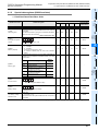
1 Device Outline
1.1 Devices Constructing PLC
1
Device Outline
1.
Device Outline
2
This chapter explains basic contents of devices.
Devices in
Detail
1.1
Devices Constructing PLC
3
Specified the
Device &
Constant
Each PLC has many built-in relays, timers, counters, etc.
Each of which has many normally-open contacts and normally-closed contacts.
Connect these contacts and coils to construct a program.
Each PLC also has built-in memory devices including data registers (D) and extension registers (R) to store
numeric data.
4
Special Device
5
Errors
6
Types and
Setting of
Parameters
7
Other Functions
13
FXCPU Structured Programming Manual
1 Device Outline
[Device & Common]
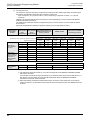
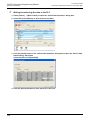
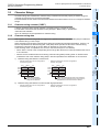
1.1.1
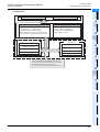
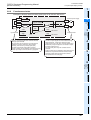
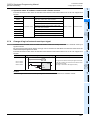
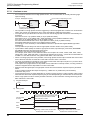
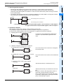
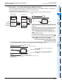
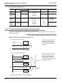
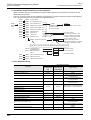
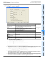
1.1 Devices Constructing PLC
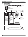
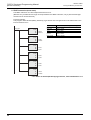
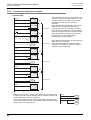
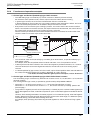
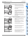
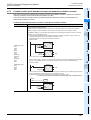
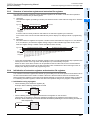
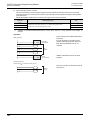
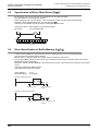
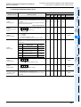
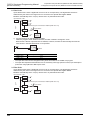
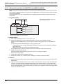
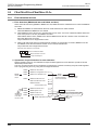
Relation among devices
Arrow indicates signal transfer.
Input terminal or
input connector
Input relay: X
The PLC receives signals from external input switches via input relays.
The symbol of input relay is "X".
The PLC has built-in input relays in accordance with its scale.
1 2 3 4
Counter: C
The PLC has many
built-in counters.
The symbol of
counter is "C".
Auxiliary relay: M
The PLC has many
built-in auxiliary
relays.
The symbol of
auxiliary relay is "M".
State relay: S
The PLC has many
built-in state relays.
The symbol of state
relay is "S".
Timer: T
The PLC has many
built-in timers.
The symbol of timer
is "T".
Output relay: Y
The PLC drives
external loads via
output relays.
The PLC has many
built-in output relays.
The symbol of
output relay is "Y".
Contact (one normally-open contact) for external output of output relay
The PLC has built-in output contacts in accordance with its scale.
Output terminal or
output connector
14
FXCPU Structured Programming Manual
[Device & Common]
1.1 Devices Constructing PLC
1
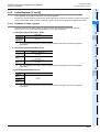
Device function list
1. Input relay (X) and output relay (Y)
→ Refer to Section 2.2.
• Digital filters are used in specified input relays, and the filter value can be changed in programs.
Accordingly, assign input relay numbers having input filter for applications requiring high-speed receiving.
(Refer to explanation of filter adjustment, input interrupt, high speed counter and various instructions.)
→ Refer to Section 2.3.
• Auxiliary relays are built in the PLC. Different from input relays and output relays, auxiliary relays cannot
receive external inputs or cannot drive external loads directly.
Auxiliary relays are available only in programs.
3. State relay (S)
→ Refer to Section 2.4.
• State relays are used as process numbers in the step ladder.
• State relays can be used as annunciators for external failure diagnosis.
5
Errors
• If state relays are not used as process numbers, they can be programmed as general contacts/coils in the
same way as auxiliary relays.
4
Special Device
• In some auxiliary relays, the ON/OFF status is backed up against interruption of the PLC power.
3
Specified the
Device &
Constant
2. Auxiliary relay (M)
2
Devices in
Detail
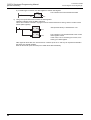
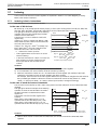
• In the PLC main unit, input relays and output relays are assigned with serial octal numbers such as "X000
to X007", "X010 to X017", "Y000 to Y007" and "Y010 to Y017".
In extension units and extension blocks, input relays and output relays are also assigned with serial octal
numbers in the connection order from the PLC main unit.
Device Outline
1.1.2
1 Device Outline
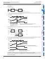
4. Timer (T)
→ Refer to Section 2.5.
6
Types and
Setting of
Parameters
• Timers count clock pulses (1 ms, 10 ms, 100 ms, etc.) inside the PLC.
When the count value reaches the set value, output contacts are activated.
Timers can measure 0.001 to 3276.7 seconds in accordance with the base clock pulse.
5. Counter (C)
Counters are classified into the following types, and can be used for suitable purposes and applications.
1) Counter (latched type)
2) High speed counter (latched type backed up against power interruption)
→ Refer to Section 2.7.
High speed counters can count several kHz without regard to operations in the PLC.
- 32-bit counter: For up/down-counting, counting range: -2,147,483,648 to +2,147,483,647
(1-phase 1-counting, 1-phase 2 counting or 2-phase 2 counting) assigned to specific input relays
6. Data register (D)
→ Refer to Section 2.8.
Data registers store numeric data.
FX PLCs have only 16-bit data registers (whose most significant bit indicates the positive or negative sign),
but two combined data registers can handle 32-bit numeric value (whose most significant bit indicates the
positive or negative sign). (Refer to "5. Counter" for the available numeric range.)
Data registers are classified into the general type and the latched type (backed up against power interruption)
in the same way as other devices.
15
7
Other Functions
→ Refer to Section 2.6.
Counters are used for signals inside the PLC. The response speed is several tens of Hz or less usually.
- 16-bit counter: For up-counting, counting range: 1 to 32767
- 32-bit counter: For up/down-counting, counting range: -2,147,483,648 to +2,147,483,647
FXCPU Structured Programming Manual
[Device & Common]
1 Device Outline
1.1 Devices Constructing PLC
7. Extension register (R) and extension file register (ER)
→ Refer to Section 2.9.
Only FX3G/FX3GC/FX3U/FX3UC PLCs support extension registers (R) and extension file registers (ER).
Extension registers(R) are extended type of data registers (D), and backed up against power interruption by
battery in FX3U/FX3UC PLCs.
In FX3G/FX3GC PLCs, general type devices can be backed up against power interruption if an optional battery
is connected.
FX3G/FX3GC/FX3U/FX3UC PLCs can store the contents of extension registers (R) in extension file registers
(ER). However, FX3U/FX3UC PLCs can use extension file registers (ER) only while a memory cassette is
attached.
8. Index register (V and Z)
→ Refer to Section 2.10.
Registers (V) (Z) are available for indexing.
Add index registers (V) (Z) to other devices as follows:
[In the case of "V0 = 5, Z0 = 5]
D100V0 = D105, C20Z0 = C25 ← Device number + Value of V or Z
Data registers and index registers are used to indirectly specify set values of timers and counters, or used in
instructions.
9. Pointer (P and I)
→ Refer to Section 2.11.
Pointers are classified into the branch type and the interrupt type.
• Branch pointers (P) specify the jump destination of the CJ (FNC 00: Conditional jump) and CALL
(subroutine call) instructions.
• Interrupt pointers (I) specify the interrupt routine for input interrupt, timer interrupt or counter interrupt.
10.Constant (K, H and E)
→ Refer to Chapter 3.
Among various numeric values used in PLCs, "K" indicates "decimal integer", "H" indicates "hexadecimal
value", and "E" indicates "real number (floating point data)".
Constants are used for set values and current values of timers and counters as well as input variables of
instructions.
16
FXCPU Structured Programming Manual
1 Device Outline
[Device & Common]
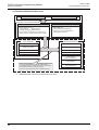
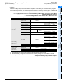
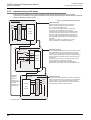
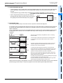
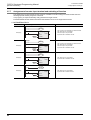
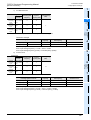
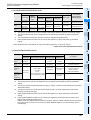
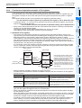
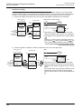
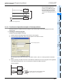
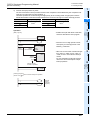
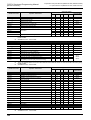
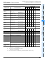
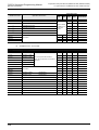
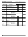
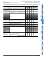
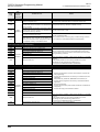
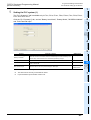
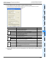
1.2 Program Memory and Devices
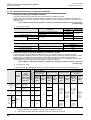
Program Memory and Devices
1.2.1
Memory structure
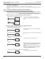
Device Outline
1.2
1
2
CPU
Devices in
Detail
1. FX3U and FX3UC PLCs
System ROM
3
Built-in device memory(RAM)
Specified the
Device &
Constant
[Bit device memory]
[Data memory]
Contact image memory
Input relay (X)
Output relay (Y)
Auxiliary relay (M) State relay (S)
Timer contact, time counting coil,
counter contact, counting coil and reset coil
Data register (D)
Timer current value register (T)
Counter current value register (C)
Index register (V and Z)
4
Extension register (R)
Parameter
Sequence program
Sequence program
Comment
Comment
File register (D)
File register (D)
Special setting
Special setting
Symbolic information*1
Symbolic information*1
*1. Supported in Ver. 3.00 or later.
6
Types and
Setting of
Parameters
Extension file register (ER)
5
Errors
Parameter
Special Device
Optional memory
(Flash memory)
Transfer/initialization by instruction
Built-in program memory(RAM)
7
Other Functions
The PLC automatically recognizes attachment of
an optional memory (when the power is turned ON),
and isolates the built-in program memory.
(The PLC gives the priority to the optional memory.)
17
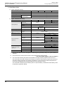
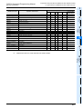
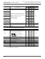
FXCPU Structured Programming Manual
1 Device Outline
[Device & Common]
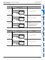
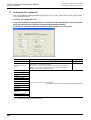
1.2 Program Memory and Devices
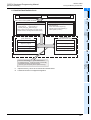
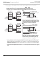
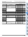
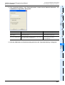
2. FX3G and FX3GC PLCs
CPU
System ROM
Built-in device memory(RAM, EEPROM)
[Bit device memory]
Contact image memory
Input relay (X)
Output relay (Y)
Auxiliary relay (M) State relay (S)
Timer contact, time counting coil, reset coil (T),
counter contact, counting coil and reset coil (C)
[Data memory]
Data register (D)
Timer current value register (T)
Counter current value register (C)
Index register (V and Z)
Extension register (R)
Parameter
Parameter
Sequence program
Sequence program
Comment
Comment
File register (D)
File register (D)
Special setting
Special setting
Extension file register (ER)
Transfer/initialization
by instruction
The PLC automatically recognizes attachment of
an optional memory*1 (when the power is turned ON),
and isolates the built-in program memory.
(The PLC gives the priority to the optional memory.)
*1.
18
Optional memory cannot be connected to FX3GC PLCs.
Extension file register (ER)
Transfer/initialization by instruction
Optional memory*1
(EEPROM)
Built-in program memory(EEPROM)
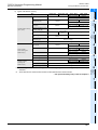
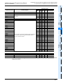
FXCPU Structured Programming Manual
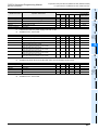
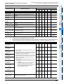
1 Device Outline
[Device & Common]
1.2 Program Memory and Devices
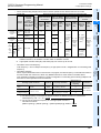
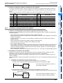
1
CPU
Device Outline
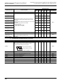
3. FX3S PLCs
System ROM
2
Built-in device memory(RAM, EEPROM)
Contact image memory
Input relay (X)
Output relay (Y)
Auxiliary relay (M) State relay (S)
Timer contact, time counting coil, reset coil (T),
counter contact, counting coil and reset coil (C)
Devices in
Detail
[Bit device memory]
[Data memory]
Data register (D)
Timer current value register (T)
Counter current value register (C)
Index register (V and Z)
Parameter
Optional memory
(EEPROM)
4
Parameter
Special Device
Sequence program
Specified the
Device &
Constant
Built-in program memory(EEPROM)
3
Sequence program
Comment
File register (D)
Comment
File register (D)
5
Errors
The PLC automatically recognizes attachment of
an optional memory (when the power is turned ON),
and isolates the built-in program memory.
(The PLC gives the priority to the optional memory.)
6
Types and
Setting of
Parameters
7
Other Functions
19
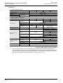
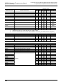
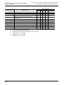
FXCPU Structured Programming Manual
1 Device Outline
[Device & Common]
1.2 Program Memory and Devices
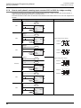
4. FX1S/FX1N/FX2N/FX1NC/FX2NC PLCs
CPU
System ROM
Built-in device memory(RAM, EEPROM)
[Bit device memory]
Contact image memory
Input relay (X)
Output relay (Y)
Auxiliary relay (M) State relay (S)
Timer contact, time counting coil, reset coil (T),
counter contact, counting coil and reset coil (C)
[Data memory]
Data register (D)
Timer current value register (T)
Counter current value register (C)
Index register (V and Z)
Built-in program memory
(RAM, EEPROM)
Optional memory *1
(RAM,EEPROM,EPROM)
Parameter
Parameter
Sequence program
Sequence program
Comment
Comment
File register (D)
File register (D)
Clock function
(FX2NC-EEPROM16C)
Extension function
(FX2N-ROM-E1)
The PLC automatically recognizes attachment of
an optional memory*1 (when the power is turned ON),
and isolates the built-in program memory.
(The PLC gives the priority to the optional memory.)
*1.
20
Optional memory cannot be connected to FX1NC PLCs.
Clock function + Extension function
(FX2NC-ROM-CE1)
FXCPU Structured Programming Manual
1 Device Outline
[Device & Common]
1.2 Program Memory and Devices
1
CPU
Device Outline
5. FX0S/FX0/FX0N/FXU/FX2C PLCs
System ROM
2
Built-in device memory(RAM, EEPROM)
Contact image memory
Input relay (X)
Output relay (Y)
Auxiliary relay (M) State relay (S)
Timer contact, time counting coil, reset coil (T),
counter contact, counting coil and reset coil (C)
Devices in
Detail
[Bit device memory]
[Data memory]
Data register (D)
Timer current value register (T)
Counter current value register (C)
Index register (V and Z)
Parameter
Parameter
Sequence program
Sequence program
Comment
Comment
File register (D)*2
File register (D)*2
4
Special Device
Optional memory *1
(RAM,EEPROM,EPROM)
Specified the
Device &
Constant
Built-in program memory
(RAM, EEPROM)
3
5
Errors
The PLC automatically recognizes attachment of
an optional memory*1 (when the power is turned ON),
and isolates the built-in program memory.
(The PLC gives the priority to the optional memory.)
Optional memory cannot be connected to FX0S/FX0 PLCs.
*2.
FX0S/FX0 PLCs do not support file registers.
Types and
Setting of
Parameters
*1.
6
7
Other Functions
21
FXCPU Structured Programming Manual
1 Device Outline
[Device & Common]
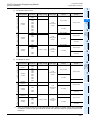
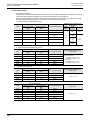
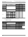
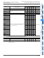
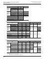
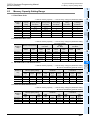
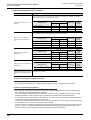
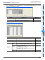
1.2.2
1.2 Program Memory and Devices
Memory operations and backup against power interruption (power ON/OFF and
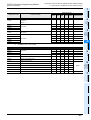
RUN/STOP)
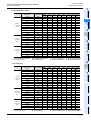
1. FX3U/FX3UC PLCs
1) Types of program memory
Item
Power OFF
Power OFF→ON
STOP→RUN
Does not
Sequence program
Does not change.*2
Does not change.*2
Comment
File register
Can be secured by
parameter setting.
Does not change.*2
Does not change.*2
Special setting
Symbolic
RUN→STOP
change.*2
Parameter
information*1
Does not change.*2
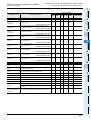
2) Types of word device memory
Item
Power OFF
General type
Data register (D)
Extension file register
(ER)*5
Index register (V and Z)
Timer current value
register (T)
Clock data
22
RUN→STOP
Cleared.
Does not change while M8033 is ON.
Does not change.*2
Cleared.
Set to initial
Does not change.*4
value.*4
Does not change.*3
Latched (backed-up) type
File type
V, Z
STOP→RUN
Does not change.
Does not change.*3
File type
Does not change.
Cleared.
For 100 ms
Cleared.
For 10 ms
Cleared.
Does not change.
Does not change.
Does not change.
Cleared.
Does not change while M8033 is ON.
Does not change.*3
Retentive type for 1 ms
Does not change.*3
Cleared.
Cleared.
Does not change while M8033 is ON.
Retentive type for 100 ms
General type
Counter current value
register (C)
Cleared.
Latched (backed-up) type
Special type
Extension register (R)
Power OFF→ON
Does not change.
Cleared.
Does not change while M8033 is ON.
Latched (backed-up) type
Does not change.*3
High speed type
Does not change.*3
Current value
Does not change.*3
*1.
Available in Ver. 3.00 or later.
*2.
The program memory contents or device status is not held correctly when the battery voltage
becomes lower than the holding voltage if a memory cassette is not attached.
*3.
The device status is not held correctly when the battery voltage becomes lower than the holding
voltage.
*4.
Some devices are cleared when the PLC mode switches from STOP to RUN.
→ For special data registers, refer to Chapter 4.
*5.
An optional memory cassette is required.
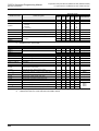
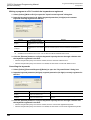
FXCPU Structured Programming Manual
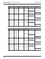
1 Device Outline
[Device & Common]
1.2 Program Memory and Devices
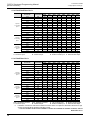
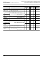
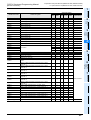
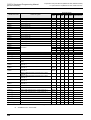
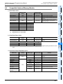
Item
Power OFF
Input relay (X)
Cleared.
General type auxiliary
relay (M)
Cleared.
Latched (backed-up) type
auxiliary relay (M)
General type state relay
(S)
Does not change while M8033 is ON.
Does not change.
Cleared.
Does not change while M8033 is ON.
Cleared.
Set to initial
Cleared.
Does not change.
Cleared.
Does not change while M8033 is ON.
Does not change.
Cleared.
For 100 ms
Cleared.
For 10 ms
Cleared.
Does not change.
Cleared.
Does not change while M8033 is ON.
Does not change.
5
Cleared.
Does not change while M8033 is ON.
Does not change.
Cleared.
Does not change while M8033 is ON.
Does not change.
Retentive type for 1 ms
Does not change.
Does not change.
Cleared.
Does not change while M8033 is ON.
Latched (backed-up) type
Does not change.
High speed type
Does not change.
6
Types and
Setting of
Parameters
Retentive type for 100 ms
Cleared.
3
4
Does not change.*1
value.*1
Annunciator (S)
General type
Cleared.
Errors
Counter contact
Counting coil
Reset coil (C)
Does not change.
Does not change.
Latched (backed-up) type
state relay (S)
Timer contact
Time counting coil
Reset coil (T)
Does not change while M8033 is ON.
Special Device
Special auxiliary relay (M)
RUN→STOP
Does not change.
Cleared.
Output relay (Y)
STOP→RUN
Specified the
Device &
Constant
Contact image memory
(X, Y, M, S)
Power OFF→ON
2
Devices in
Detail
3) Types of bit device memory
1
Device Outline
• Caution
When the battery voltage becomes low due to expiration of the battery life or another reason, programs
(not stored in a memory cassette), latched (backed-up) type devices and clock data are not held correctly.
Clear latched type devices, and transfer programs (not stored in a memory cassette) again. In addition, set
the initial values and clock data if necessary.
→ For rough guide to the life and replacement timing of the battery, refer to the User's Manual
[Hardware Edition] of each PLC.
→ For the latched type device clear method, refer to Subsection 1.2.5.
7
Some devices are cleared when the PLC mode switches from STOP to RUN.
*2.
When the battery voltage becomes lower than the holding voltage, the device status is not held
correctly.
→ For special auxiliary relays, refer to Chapter 4.
23
Other Functions
*1.
FXCPU Structured Programming Manual
1 Device Outline
[Device & Common]
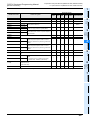
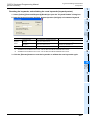
1.2 Program Memory and Devices
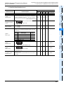
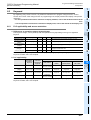
2. FX3G/FX3GC PLCs
1) Types of program memory
Item
Power OFF
Power OFF→ON
STOP→RUN
Parameter
Does not change.
Sequence program
Does not change.
Comment
File register
RUN→STOP
Does not change.
Can be secured by
parameter setting.
Does not change.
2) Types of word device memory
Item
Power OFF
Cleared.*1
General type
Data register (D)
Latched (backed-up) type
Extension file register
(ER)
Index register (V and Z)
Timer current value
register (T)
General type
Clock data
24
Cleared.
Does not change while M8033 is ON.
Does not change.
Cleared.
Does not change.*2
value.*2
Cleared.*1
Does not change.
Does not change.
Cleared.
For 100 ms
Cleared.
For 10 ms
Cleared.
For 1 ms
Cleared.
Does not change.
Does not change.
Does not change.
Does not change.
Cleared.
Does not change while M8033 is ON.
Retentive type for 1 ms
Does not change.
Does not change.
Cleared.
Does not change while M8033 is ON.
Latched (backed-up) type
Does not change.
High speed type
Does not change.
Current value
Cleared.
Does not change while M8033 is ON.
Does not change.
Cleared.
Cleared.
Does not change while M8033 is ON.
Retentive type for 100 ms
General type
Counter current value
register (C)
RUN→STOP
Set to initial
File type
V, Z
STOP→RUN
Does not change.
Does not change.
File type
Special type
Extension register (R)
Power OFF→ON
Does not change.*3
*1.
General type devices can be changed to the latched type by parameter setting if an optional battery is
attached.
*2.
Some devices are cleared when the PLC mode switches from STOP to RUN.
→ For special data registers, refer to Chapter 4.
*3.
The clock data is held by the power accumulated in the large-capacity capacitor built in the PLC.
The clock data is not held correctly if the voltage of the built-in large-capacity capacitor becomes low.
The large-capacity capacitor can hold the clock data for 10 days (when the ambient temperature is
25°C) if it is charged fully (by turning ON the PLC for 30 minutes or more).
The clock data is backed up by the battery when an optional battery is attached and the battery mode
is selected by parameter setting.
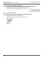
FXCPU Structured Programming Manual
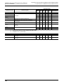
1 Device Outline
[Device & Common]
1.2 Program Memory and Devices
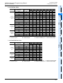
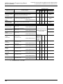
1
Item
Power OFF
Input relay (X)
Cleared.
Output relay (Y)
Cleared.
Special auxiliary relay (M)
Does not change.
Cleared.
Does not change while M8033 is ON.
2
Does not change.
Cleared.
Set to initial
Cleared.*1
Does not change.
Does not change.
Annunciator (S)
Does not change.
For 100 ms
Cleared.
For 10 ms
Cleared.
For 1 ms
Cleared.
Does not change.
Cleared.
Does not change while M8033 is ON.
Does not change.
Cleared.
Does not change while M8033 is ON.
Does not change.
Cleared.
Does not change while M8033 is ON.
Retentive type for 100 ms
Does not change.
Retentive type for 1 ms
Does not change.
Cleared.
3
Does not change.*2
value.*2
Latched (backed-up) type
state relay (S)
General type
Cleared.
Does not change while M8033 is ON.
Does not change.
Cleared.
4
5
Errors
Counter contact
Counting coil
Reset coil (C)
Does not change.
Special Device
Timer contact
Time counting coil
Reset coil (T)
Cleared.
Specified the
Device &
Constant
General type state relay
(S)
RUN→STOP
Does not change while M8033 is ON.
Cleared.*1
Latched (backed-up) type
auxiliary relay (M)
STOP→RUN
Does not change.
Devices in
Detail
General type auxiliary
relay (M)
Contact image memory
(X, Y, M, S)
Power OFF→ON
Device Outline
3) Types of bit device memory
Does not change while M8033 is ON.
Latched (backed-up) type
Does not change.
High speed type
Does not change.
General type devices can be changed to the latched type by parameter setting if an optional battery is
attached.
*2.
Some devices are cleared when the PLC mode switches from STOP to RUN.
→ For special auxiliary relays, refer to Chapter 4.
6
Types and
Setting of
Parameters
*1.
7
Other Functions
25
FXCPU Structured Programming Manual
1 Device Outline
[Device & Common]
1.2 Program Memory and Devices
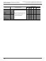
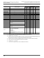
3. FX3S PLC
1) Types of program memory
Item
Power OFF
Power OFF→ON
STOP→RUN
Parameter
Does not change.
Sequence program
Does not change.
Comment
File register
RUN→STOP
Does not change.
Can be secured by
parameter setting.
Does not change.
2) Types of word device memory
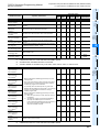
Item
Power OFF
General type
Data register (D)
Timer current value
register (T)
Counter current value
register (C)
26
STOP→RUN
RUN→STOP
Does not change.
Cleared.
Does not change while M8033 is ON.
Does not change.
File type
Does not change.
Set to initial
Cleared.
Does not change.*1
value.*1
V, Z
Cleared.
For 100 ms
Cleared.
For 10 ms
Cleared.
For 1 ms
Cleared.
Does not change.
Does not change.
Does not change.
Does not change.
Does not change.
Latched (backed-up) type
Current value
Cleared.
Does not change while M8033 is ON.
Retentive type for 1 ms
Cleared.
Cleared.
Does not change while M8033 is ON.
Does not change.
General type
Cleared.
Does not change while M8033 is ON.
Retentive type for 100 ms
High speed type
Clock data
Cleared.
Latched (backed-up) type
Special type
Index register (V and Z)
Power OFF→ON
Does not change.
Cleared.
Does not change while M8033 is ON.
Does not change.
Does not change.
Does not change.*2
*1.
Some devices are cleared when the PLC mode switches from STOP to RUN.
→ For special data registers, refer to Chapter 4.
*2.
The clock data is held by the power accumulated in the large-capacity capacitor built in the PLC.
The clock data is not held correctly if the voltage of the built-in large-capacity capacitor becomes low.
The large-capacity capacitor can hold the clock data for 10 days (when the ambient temperature is
25°C) if it is charged fully (by turning ON the PLC for 30 minutes or more).
FXCPU Structured Programming Manual
1 Device Outline
[Device & Common]
1.2 Program Memory and Devices
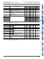
1
Item
Power OFF→ON
Input relay (X)
Cleared.
Output relay (Y)
Cleared.
General type auxiliary
relay (M)
Cleared.
Latched (backed-up) type
auxiliary relay (M)
Special auxiliary relay (M)
*1.
For 1 ms
Does not change.
Set to initial
Cleared.
2
3
Does not change. *1
value.*1
Cleared.
Does not change.
Does not change.
Cleared.
Cleared.
Cleared.
Does not change.
Does not change.
Cleared.
Does not change while M8033 is ON.
Does not change.
Cleared.
Does not change while M8033 is ON.
Does not change.
Does not change.
Cleared.
Cleared.
Does not change while M8033 is ON.
Retentive type for 1 ms
Latched (backed-up) type
Cleared.
Does not change while M8033 is ON.
Retentive type for 100 ms
General type
Cleared.
Does not change while M8033 is ON.
Does not change.
Cleared.
Does not change while M8033 is ON.
4
5
Errors
Counter contact
Counting coil
Reset coil (C)
For 10 ms
Does not change.
Special Device
Timer contact
Time counting coil
Reset coil (T)
Cleared.
Does not change while M8033 is ON.
Does not change.
Latched (backed-up) type
state relay (S)
For 100 ms
RUN→STOP
Specified the
Device &
Constant
General type state relay
(S)
STOP→RUN
Does not change.
Devices in
Detail
Contact image memory
(X, Y, M, S)
Power OFF
Device Outline
3) Types of bit device memory
Does not change.
Some devices are cleared when the PLC mode switches from STOP to RUN.
→ For special data registers, refer to Chapter 4.
6
Types and
Setting of
Parameters
7
Other Functions
27
FXCPU Structured Programming Manual
1 Device Outline
[Device & Common]
1.2 Program Memory and Devices
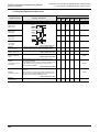
4. FX1S/FX1N/FX2N/FX1NC/FX2NC PLCs
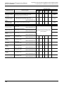
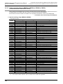
The memory type varies depending on the PLC, and is classified as follows by the device initialization timing.
Classification
A1: Backed up by battery
A: Latched type memory
Power OFF
STOP→RUN
RUN→STOP
Does not change.
(The device status is not held correctly when the battery voltage becomes
lower than the holding voltage.)
A2: Backed up by EEPROM
Does not change.
A3: Backed up by capacitor
Does not change.
(The device status is held correctly for 10 days (when the ambient temperature is 25°C) after the capacitor is fully charged, but the device status is not
held correctly after the capacitor is discharged.)
B: Special device and index memory
Cleared.
C: Non-latched type memory
*1.
Power OFF→ON
Set to initial
Does not change.*1
value.*1
Cleared.
Does not change.
Cleared.
Does not change while M8033 is ON.
Some devices are cleared when the PLC mode switches from STOP to RUN.
1) Types of program memory
FX1S
FX1N
FX2N
FX1NC
FX2NC
Parameter
Item
A2
A2
A1*1
A2
A1*1
Sequence program
A2
A2
A1*1
A2
A1*1
A2
A2
A1*1
A2
A1*1
A2
A2
A1*1
A2
A1*1
Comment
File register
*1.
Can be secured by
parameter setting.
The battery is not used when an optional EEPROM or EPROM memory is attached.
2) Types of word device memory
Item
Data register (D)
Index register (V and Z)
Timer current value
register (T)
Counter current value
register (C)
Clock data
*1.
28
FX1S
FX1N
FX2N
FX1NC
General type
C
C
C
C
FX2NC
C
Latched (backed-up) type
A2
A2/A3
A1
A2/A3
A1
File type*1
A2
A2
A1
A2
A1
Special type
B
B
B
B
B
V, Z
B
B
B
B
B
For 100 ms
C
C
C
C
C
For 10 ms
C
C
C
C
C
Retentive type for 100 ms
-
A3
A1
A3
A1
Retentive type for 1 ms
-
A3
A1
A3
A1
General type
C
C
C
C
C
Latched (backed-up) type
A2
A2/A3
A1
A2/A3
A1
High speed type
A2
A2
A1
A2
A1
Current value
A3
A3
A1
A3
A1*1
Attach a memory board having the clock function when the clock function is required in the FX2NC
Series.
FXCPU Structured Programming Manual
1 Device Outline
[Device & Common]
1.2 Program Memory and Devices
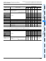
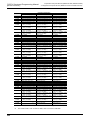
1
Contact image memory
(X, Y, M, S)
FX2N
FX1NC
FX2NC
C
C
C
C
Output relay (Y)
C
C
C
C
C
General type auxiliary
relay (M)
C
C
C
C
C
2
Latched (backed-up) type
auxiliary relay (M)
A2
A2/A3
A1
A2/A3
A1
Special auxiliary relay (M)
B
B
B
B
B
General type state relay
(S)
A2
A2/A3
C
A2/A3
C
Latched (backed-up) type
state relay (S)
A2
A2/A3
A1
A2/A3
A1
Annunciator (S)
-
-
A1
-
A1
For 100 ms
C
C
C
C
C
For 10 ms
C
C
C
C
C
Retentive type for 100 ms
-
A3
A1
A3
A1
Retentive type for 1 ms
-
A3
A1
A3
A1
General type
C
C
C
C
C
Latched (backed-up) type
A2
A2/A3
A1
A2/A3
A1
High speed type
A2
A2
A1
A2
A1
3
4
Special Device
Counter contact
Counting coil
Reset coil (C)
FX1N
C
Specified the
Device &
Constant
Timer contact
Time counting coil
Reset coil (T)
FX1S
Input relay (X)
Devices in
Detail
Item
Device Outline
3) Types of bit device memory
5
Errors
6
Types and
Setting of
Parameters
7
Other Functions
29
FXCPU Structured Programming Manual
1 Device Outline
[Device & Common]
1.2 Program Memory and Devices
5. FX0S/FX0/FX0N/FXU/FX2C PLCs
1) Types of program memory
Item
Power OFF
Power OFF→ON
STOP→RUN
Parameter
Does not
Sequence program
Does not change.*2
Comment
File register
RUN→STOP
change.*2
Does not change.*2
Can be secured by
parameter setting.
Does not change.*2
2) Types of word device memory
Item
Power OFF
General type
Data register (D)
Index register (V and Z)
Timer current value
register (T)
Clock data
30
Cleared.
STOP→RUN
RUN→STOP
Does not change.
Cleared.
Does not change while M8033 is ON.
Latched (backed-up) type
Does not change.*2
File type
Does not change*2.
Special type
Cleared.
V, Z
Cleared.
Set to initial
Does not change.*1
value.*1
Set to initial
Does not change.*1
value.*1
For 100 ms
Cleared.
For 10 ms
Cleared.
Does not change.
Does not change.
Cleared.
Does not change while M8033 is ON.
Does not change.*2
Retentive type for 1 ms
Does not change.*2
Cleared.
Cleared.
Does not change while M8033 is ON.
Retentive type for 100 ms
General type
Counter current value
register (C)
Power OFF→ON
Does not change.
Cleared.
Does not change while M8033 is ON.
Latched (backed-up) type
Does not change.*2
High speed type
Does not change.*2
Current value
Does not change.*2
*1.
Some devices are cleared when the PLC mode switches from STOP to RUN.
M8074 is backed up against power interruption.
*2.
The device status is not held correctly when the battery voltage becomes lower than the holding
voltage.
(FXU/FX2C PLCs)
FXCPU Structured Programming Manual
1 Device Outline
[Device & Common]
1.2 Program Memory and Devices
1
Item
Input relay (X)
Cleared.
Output relay (Y)
Cleared.
General type auxiliary
relay (M)
Cleared.
Latched (backed-up) type
auxiliary relay (M)
Special auxiliary relay (M)
RUN→STOP
Cleared.
Does not change while M8033 is ON.
Does not change.
Does not change.
Cleared.
Does not change while M8033 is ON.
2
Does not change.*2
Cleared.
Set to initial
Cleared.
Does not change.
Annunciator (S)
Does not change.*2
Cleared.
For 10 ms
Cleared.
Does not change.
Cleared.
Does not change while M8033 is ON.
Does not change.
Cleared.
Does not change while M8033 is ON.
Retentive type for 100 ms
Does not change.*2
Retentive type for 1 ms
Does not change.*2
Does not change.
Cleared.
Does not change while M8033 is ON.
Latched (backed-up) type
Does not change.*2
High speed type
Does not change.*2
Some devices are cleared when the PLC mode switches from STOP to RUN.
M8074 is backed up against power interruption.
*2.
The device status is not held correctly when the battery voltage becomes lower than the holding
voltage.
(FXU/FX2C PLCs)
5
6
Types and
Setting of
Parameters
*1.
4
Errors
Cleared.
Cleared.
Does not change while M8033 is ON.
Does not change.*2
For 100 ms
3
Does not change.*1
value.*1
Latched (backed-up) type
state relay (S)
General type
Cleared.
Does not change while M8033 is ON.
Special Device
Counter contact
Counting coil
Reset coil (C)
STOP→RUN
Does not change.
Specified the
Device &
Constant
General type state relay
(S)
Timer contact
Time counting coil
Reset coil (T)
Power OFF→ON
Devices in
Detail
Contact image memory
(X, Y, M, S)
Power OFF
Device Outline
3) Types of bit device memory
7
Other Functions
31
FXCPU Structured Programming Manual
1 Device Outline
[Device & Common]
1.2.3
1.2 Program Memory and Devices
Types of backup methods against power interruption
There are following types of latch (backup) of the program memory and built-in devices in PLCs.
1. Battery backup method
FXU/FX2C/FX2N/FX2NC/FX3G/FX3GC/FX3U/FX3UC PLCs
Item
Description
Latched (backed-up) contents
A battery backs up the built-in RAM memory, latched type devices and clock data.
Maintenance
Periodical replacement is required.
For rough guide to the replacement frequency, refer to the User's Manual [Hardware Edition] of each
PLC.
Cautions
1) When the battery voltage becomes low, sequence programs and other latched (backed-up)
contents are lost.
2) When an optional memory cassette (flash memory) is attached, it is not necessary to back up
sequence programs using the battery (in FX3U/FX3UC PLCs).
2. Flash memory backup method
FX3U/FX3UC PLCs
Item
Description
Latched (backed-up) contents
1) The flash memory built in a memory cassette holds sequence programs.
2) A battery is used also to hold latched (backed-up) type devices and clock data.
Maintenance
Maintenance is not required.
Cautions
The upper limit is set for the number of times of overwriting.
(Refer to the User's Manual [Hardware Edition] of each PLC.)
3. EEPROM backup method
FX0S/FX0N/FX1S/FX1N/FX1NC/FX3S/FX3G/FX3GC PLCs
Item
Description
Latched (backed-up) contents
1) The EEPROM built in the PLC holds sequence programs and latched (backed-up) type devices.
2) A capacitor is used also to hold the clock data.
Maintenance
Maintenance is not required.
Cautions
1) The upper limit is set for the number of times of overwriting.
(Refer to the User's Manual [Hardware Edition] of each PLC.)
2) For secure backup, it is necessary to keep the PLC power ON for 5 minutes or more, and then turn
OFF the power.
4. Capacitor backup method
FX1N/FX1NC PLCs
Item
32
Description
Latched (backed-up) contents
1) The large-capacity capacitor built in the PLC holds latched (backed-up) type devices and clock
data.
2) The capacitor holds data for 10 days (when the ambient temperature is 25°C) if it is fully charged
as described below.
Maintenance
Maintenance is not required.
Cautions
1) The large-capacity capacitor is charged while the PLC is ON, and fully charged after the PLC is
ON for 30 minutes or more.
2) When the voltage of the large-capacity capacitor becomes low, latched (backed-up) type devices
are not held correctly.
When using the PLC for the first time after purchase, or when using the PLC after power OFF for a
long time (10 days [when the ambient temperature is 25°C] in the fully charged status), clear
latched (backed-up) type devices.
FXCPU Structured Programming Manual
[Device & Common]
1.2 Program Memory and Devices
1
Change of devices between general type and latched (backed-up) type
FX0S/FX0/FX0N/FX1S/FX1N/FX1NC/FX3S/FX3G*1/FX3GC*1 PLCs do not support the type change of latched
(backed-up) type devices.
1. When using latched (backed-up) type devices as non-latched type devices
2. When using non-latched type devices as latched (backed-up) type devices
3
Non-latched type devices can be changed into the latched (backed-up) type by parameter setting.
1.2.5
In FX3G/FX3GC PLCs, non-latched type devices can be changed into the latched (backed-up) type by
selecting the battery mode using a parameter if an optional battery is attached.
How to initialize latched (backed-up) type devices
Specified the
Device &
Constant
*1.
2
Devices in
Detail
Some latched (backed-up) type devices can be changed into the non-latched type by parameter setting.
Devices dedicated to the latched type cannot be changed into the non-latched type.
Such devices can be handled as non-latched type devices by clearing all latched type devices using the initial
pulse (M8002) in a program.
Device Outline
1.2.4
1 Device Outline
4
1. M8032 (latched type memory all clear)
5
Errors
When M8032 is set to ON, all latched (backed-up) devices*1 (including reset coils of timers and counters) are
cleared.
M8032 can be set to ON and OFF using the forced ON/OFF operation from peripheral equipment or in a
sequence program. Note that latched type devices cannot be set to ON while M8032 is ON.
When M8032 is set to ON in a program, note that latched type devices are cleared during execution of the
END instruction after M8032 turns ON.
Special Device
Latched (backed-up) type devices can be initialized by clearing the whole PLC memory using peripheral
equipment, clearing all latched type memories using the special auxiliary relay M8032, or executing the ZRST
instruction.
This subsection describes two major methods.
6
Types and
Setting of
Parameters
Program example:
This program clears all latched type devices.
M8002
M8032
Initial pulse
*1.
General type devices which have been changed into the latched type in the FX3G/FX3GC PLCs using
an optional battery attached are also cleared.
33
7
Other Functions
→ For details, refer to Subsection 4.2.11.
FXCPU Structured Programming Manual
1 Device Outline
[Device & Common]
1.2 Program Memory and Devices
2. ZRST instruction (zone reset)
The ZRST instruction can clear multiple devices all at once.
(Because only a limited device range can be specified for the ZRST instruction, only a part of latched type
devices can be cleared at a time.)
Program example:
This program clears latched (battery backed-up) type devices in the ranges shown in the table below in the
FX3U and FX3UC PLCs.
Latched (backed-up) device range
Clear input
EN
EN
EN
EN
EN
EN
ZRST
ENO
d1
d2
Auxiliary relay
M500
M7679
ZRST
ENO
d1
d2
S500
S4095
ZRST
ENO
d1
d2
T246
T255
ZRST
ENO
d1
d2
C100
C199
ZRST
ENO
d1
d2
C220
C255
ZRST
ENO
d1
d2
D200
D7999
M500 to M7679
State relay
S500 to S4095
Timer
T246 to T255
Counter
C100 to C199,
C220 to C255
Data register
D200 to D7999
→ For details on latched (backed-up) type devices, refer to Subsection 1.2.2
34
FXCPU Structured Programming Manual
2 Devices in Detail
[Device & Common]
2.1 Device Number List
1
Device Outline
2.
Devices in Detail
2
2.1
Devices in
Detail
This chapter explains how numeric values are handled in the PLC as well as the roles and functions of
various built-in devices including I/O relays, auxiliary relays, state relays, counters and data registers.
The following contents provide a basis for handling the PLC.
Device Number List
Device name
Reference
Device numbers are octal.
The total number of inputs and outputs is 256.
Section 2.2
I/O relay
X000 to X367
248 points
Output relay
Y000 to Y367
248 points
General type [changeable]
M0 to M499
500 points
Latched (backed-up) type
[changeable]
M500 to M1023
524 points
Latched (backed-up) type [fixed]
M1024 to M7679
6656 points
M8000 to M8511
512 points
Initial state
(General type [changeable])
S0 to S9
10 points
General type [changeable]
S10 to S499
490 points
Latched (backed-up) type
[changeable]
S500 to S899
400 points
Annunciator
(Latched (backed-up) type
[changeable])
S900 to S999
100 points
Latched (backed-up) type [fixed]
S1000 to S4095
3096 points
T0 to T191
Auxiliary relay
Special
type*2
Devices can be changed between the latched
(backed-up) type and the non-latched type using
parameters.
Section 2.3
Chapter 4
5
Errors
Input relay
4
Special Device
Description
3
Specified the
Device &
Constant
Device numbers are assigned in the FX3U and FX3UC PLCs as shown below.
The assignment varies depending on each PLC. For details, refer to the reference section.
For input relay numbers and output relay numbers when I/O extension equipment and special extension
equipment are connected to the PLC main unit, refer to the User's Manual [Hardware Edition] of each PLC.
State relay
6
Section 2.4
7
192 points
0.1 to 3276.7 sec
100 ms
T192 to T199
[for subroutine or interrupt routine]
8 points
0.1 to 3276.7 sec
10 ms
T200 to T245
46 points
0.01 to 327.67 sec
Retentive type for 1 ms
T246 to T249
4 points
0.001 to 32.767 sec
Retentive type for 100 ms
T250 to T255
6 points
0.1 to 3276.7 sec
1 ms
T256 to T511
256 points
0.001 to 32.767 sec
General type up-counter (16 bits)
[changeable]
C0 to C99
100 points
Latched (backed-up) type upcounter (16 bits) [changeable]
C100 to C199
100 points
0 to 32767 counts
Devices can be changed between the latched
(backed-up) type and the non-latched type using
parameters.
Section 2.5
Counter
General type bidirectional counter
C200 to C219
(32 bits) [changeable]
20 points
Latched (backed-up) type
bidirectional counter (32 bits)
[changeable]
15 points
C220 to C234
-2147483648 to +2147483647 counts
Devices can be changed between the latched
(backed-up) type and the non-latched type using
parameters.
Section 2.6
35
Other Functions
Timer (on-delay timer)
100 ms
Types and
Setting of
Parameters
Devices can be changed between the latched
(backed-up) type and the non-latched type using
parameters.
FXCPU Structured Programming Manual
2 Devices in Detail
[Device & Common]
2.1 Device Number List
Device name
Description
Reference
High speed counter
1-phase 1-counting input
Bidirectional (32 bits)
C235 to C245
1-phase 2-counting input
Bidirectional (32 bits)
C246 to C250
2-phase 2-counting input
Bidirectional (32 bits)
C251 to C255
Up to 8 points can be used among C235 to C255 [latched
(backed-up) type]
The setting can be changed between the latched (backed-up) type
and the non-latched type using parameters.
-2,147,483,648 to +2,147,483,647 counts
Hardware counter*1
1 phase : 100 kHz × 6 points, 10 kHz × 2 points
2 phases : 50 kHz (1-edge counting), 50 kHz (4-edge counting)
Software counter
1 phase : 40 kHz
2 phases : 40 kHz (1-edge counting), 10 kHz (4-edge counting)
Section 2.7
Data register (32 bits when used in pair form)
General type (16 bits)
[changeable]
D0 to D199
200 points
Latched (backed-up) type
(16 bits) [changeable]
D200 to D511
312 points
Latched (backed-up) type
(16 bits) [fixed] <file register>
D512 to D7999
7488 points
<D1000 to D7999> <7000 points>
Special type (16 bits)*2
D8000 to D8511
Index type (16 bits)
V0 to V7, Z0 to Z7 16 points
The setting can be changed between the
latched (backed-up) type and the non-latched
type using parameters.
Among 7488 fixed latched (backed-up) type
data registers, D1000 and later can be set as file
registers in units of 500 points using
parameters.
512 points
Section 2.8
Chapter 4
Section 2.10
Extension register/Extension file register
Extension register (16 bits)
R0 to R32767
32768 points
Backed up by a battery against power
interruption.
Extension file register (16 bits)
ER0 to ER32767
32768 points
Available only while a memory cassette is
attached.
For JUMP or CALL branch
P0 to P4095
4096 points
For CJ and CALL instructions
Input interrupt
Input delay interrupt
I0 to I5
6 points
Timer interrupt
I6 to I8
3 points
Counter interrupt
I010 to I060
6 points
For HSCS instruction
N0 to N7
8 points
For MC instruction
Section 2.9
Pointer
Section 2.11
Nesting
For master control
Constant
Decimal (K)
Hexadecimal (H)
36
16 bits
-32,768 to +32,767
32 bits
-2,147,483,648 to +2,147,483,647
16 bits
0 to FFFF
32 bits
0 to FFFFFFFF
Real number (E)
32 bits
-1.0 × 2128 to -1.0 × 2-126, 0, 1.0 × 2-126 to 1.0 × 2128
Both the decimal point expression and the exponent expression
are available.
Character string ("")
Character string
Specify characters with quotation marks.
In a constant of an instruction, up to 32 half-width characters are
available.
Chapter 3
*1.
When the FX3U-4HSX-ADP is connected to an FX3U PLC, the maximum input frequency is set as
follows:
1 phase : 200 kHz
2 phases : 100 kHz (1-edge counting), 100 kHz (4-edge counting)
*2.
For supported functions, refer to Chapter 4.
For handling of the latched (backed-up) area, refer to Section 1.2.
FXCPU Structured Programming Manual
2 Devices in Detail
[Device & Common]
1
Input/Output Relays [X and Y]
Device Outline
2.2
2.2 Input/Output Relays [X and Y]
Some input relay and output relay numbers are secured in the main unit, and others are assigned to
extension equipment according to the connection order.
Because input/output relays are numbered in octal, numeric values such as "8" and "9" do not exist.
Numbers of input/output relays
Devices in
Detail
2.2.1
2
The tables below show input relay (X) and output relay (Y) numbers. (Numbers are assigned in octal.)
1. FX3S/FX3G/FX3GC/FX3U/FX3UC PLCs
FX3U-16M
Model name
Output
Y000 to Y007 Y000 to Y017 Y000 to Y027 Y000 to Y037 Y000 to Y047 Y000 to Y077
8 points
16 points
24 points
32 points
40 points
64 points
Y000 to Y367
248 points
FX3UC-32M
Output
Y000 to Y007 Y000 to Y017 Y000 to Y037 Y000 to Y057
8 points
16 points
32 points
48 points
Y000 to Y367
248 points
When extended
Input
X000 to X017
16 points
X000 to X357
240 points
Output
Y000 to Y017
16 points
Y000 to Y357
240 points
Input
FX3G-14M
FX3G-24M
X000 to X007
8 points
X000 to X015
14 points (16)*1
Y000 to Y005
Y000 to Y011
6 points (8)*1
10 points (16)*1
When extended
X000 to X027
24 points
36 points (40)*1
X000 to X177
128 points
Y000 to Y017
16 points
Y000 to Y027
24 points
Y000 to Y177
128 points
6
128
points
in total
When extended
X000 to X017
16 points
X000 to X177
128 points
Y000 to Y017
Y000 to Y177
128 points
16 points
128
points
in total
Model name
FX3S-10M
FX3S-14M
FX3S-20M
FX3S-30M
Input
X000 to X005
6 points
X000 to X007
8 points
X000 to X013
12 points
X000 to X017
16 points
Output
Y000 to Y003
4 points
Y000 to Y005
6 points
Y000 to Y007
8 points
Y000 to Y015
14 points
7
Other Functions
Output
FX3G-60M
X000 to X043
Types and
Setting of
Parameters
Input
FX3G-40M
5
256
points
in total
Errors
FX3UC-32MT-LT(-2)
4
256
points
in total
Special Device
Input
Model name
256
points
in total
When extended
X000 to X367
248 points
Model name FX3GC-32MT/D(DSS)
*1.
FX3UC-96M
X000 to X007 X000 to X017 X000 to X037 X000 to X057
8 points
16 points
32 points
48 points
Output
FX3S PLC
FX3UC-64M
3
FX3U-128M When extended
X000 to X367
248 points
Model name
FX3GC PLC
FX3U-80M
X000 to X007 X000 to X017 X000 to X027 X000 to X037 X000 to X047 X000 to X077
8 points
16 points
24 points
32 points
40 points
64 points
FX3UC (D, DS, DSS)
PLC
FX3G PLC
FX3U-64M
Input
Model name FX3UC-16M
FX3UC-32MTLT(-2) PLC
FX3U-48M
Specified the
Device &
Constant
FX3U PLC
FX3U-32M
No
extension
A number inside ( ) indicates the number of occupied points.
The difference from the number of effective points indicates unused numbers.
37
FXCPU Structured Programming Manual
2 Devices in Detail
[Device & Common]
2.2 Input/Output Relays [X and Y]
2. FX1S/FX1N/FX1NC/FX2N/FX2NC PLCs
FX1S PLC
Model name
FX1S-10M
FX1S-14M
FX1S-20M
FX1S-30M
Input
X00 to X05
6 points
X00 to X07
8 points
X00 to X013
12 points
X00 to X17
16 points
Output
Y00 to Y03
4 points
Y00 to Y05
6 points
Y00 to Y07
8 points
Y00 to Y15
14 points
FX1N-24M
FX1N-40M
FX1N-60M
Model name
FX1N PLC
Input
X000 to X177
128 points
Output
Y000 to Y011 Y000 to Y017 Y000 to Y027
10 points
16 points
24 points
Y000 to Y177
128 points
FX2N-16M
FX2N-48M
FX2N-64M
FX2N-80M
FX2N-128M When extended
X000 to X007 X000 to X017 X000 to X027 X000 to X037 X000 to X047 X000 to X077
8 points
16 points
24 points
32 points
40 points
64 points
X000 to X267
184 points
Output
Y000 to Y007 Y000 to Y017 Y000 to Y027 Y000 to Y037 Y000 to Y077 Y000 to Y077
8 points
16 points
24 points
32 points
40 points
64 points
Y000 to Y267
184 points
FX1NC-16M
FX1NC-32M
Input
X000 to X177
128 points
Output
Y000 to Y007 Y000 to Y017
8 points
16 points
Y000 to Y177
128 points
FX2NC-16M
FX2NC-32M
256
points
in total
When extended
X000 to X007 X000 to X017
8 points
16 points
Model name
FX2NC
PLC
FX2N-32M
128
points
in total
Input
Model name
FX1NC
PLC
When extended
X000 to X015 X000 to X027 X000 to X043
14 points
24 points
36 points
Model name
FX2N PLC
No
extension
FX2NC-64M
128
points
in total
FX2NC-96M
When extended
Input
X000 to X007 X000 to X017 X000 to X037 X000 to X057
8 points
16 points
32 points
48 points
X000 to X267
184 points
Output
Y000 to Y007 Y000 to Y017 Y000 to Y037 Y000 to Y057
8 points
16 points
32 points
48 points
Y000 to Y267
184 points
256
points
in total
3. FX0S/FX0/FX0N/FXU/FX2C PLCs
FX0S/FX0
PLC
FX0N PLC
Model name
FX0S-10M
Input
X000 to X005
6 points
X000 to X007
8 points
X000 to X013
12 points
X000 to X017
16 points
Output
Y000 toY003
4 points
Y000 to Y005
6 points
Y000 to Y007
8 points
Y000 to Y015
14 points
No
extension
Model name
FX0N-24M
FX0N-40M
FX0N-60M
When extended
Input
X000 to X015
14 points
X000 to X027
24 points
X000 to X043
36 points
X000 to X127
84 points
Output
Y000 to Y011
10 points
Y000 to Y017
16 points
Y000 to Y027
24 points
Y000 to Y77
64 points
Model name
FXU PLC
FX0/FX0S-14M FX0/FX0S-20M FX0/FX0S-30M
FXU-16M
FXU-24M
FXU-32M
FXU-48M
FXU-64M
128
points
in total
FXU-80M
Input
Output
Y000 to Y007 Y000 to Y013 Y000 to Y017 Y000 to Y027 Y000 to Y037 Y000 to Y047 Y000 to Y077
8 points
12 points
16 points
24 points
32 points
40 points
64 points
Model name When extended
FXU PLC
FX2C PLC
38
FXU-128M
X000 to X007 X000 to X013 X000 to X017 X000 to X027 X000 to X037 X000 to X047 X000 to X077
8 points
12 points
16 points
24 points
32 points
40 points
64 points
Input
X000 to X267
184 points
Output
Y000 to Y267
184 points
256
points
in total
Model name
FX2C-64M
FX2C-96M
FX2C-128M
FX2C-160M
When extended
Input
X000 to X037
32 points
X000 to X057
48 points
X000 to X077
64 points
X000 to X117
80 points
X000 to X267
184 points
Output
Y000 to Y037
32 points
Y000 to Y057
48 points
Y000 to Y077
64 points
Y000 to Y117
80 points
Y000 to Y267
184 points
256
points
in total
FXCPU Structured Programming Manual
2 Devices in Detail
[Device & Common]
1
Functions and roles
Device Outline
2.2.2
2.2 Input/Output Relays [X and Y]
Examples of terminal names and wiring (sink input) are for the FX3U Series PLC.
0V
Devices in
Detail
COM1
Program example
S/S
X000
X000
2
External power supply
24V
X001
X000
Y000
Input
signal
Y000
Load
Y000
X000
3
Y000
NO contact
X000
Output terminal
Y000
PLC
NC contact
4
The PLC outputs signals to external loads through
output terminals. Contacts for external output
(output devices such as relay contacts, TRIACs and
transistors) of output relays are connected to output
terminals inside the PLC.
An output relay has many NO contacts and NC
contacts.
These contacts can be arbitrarily used inside the PLC.
Differences in operations between external output
contacts (output devices) and internal contacts
are explained on the next page.
Special Device
The PLC receives signals from external switches
through input terminals.
An input relay (X) connected to an input terminal
inside the PLC is an electronic relay isolated
optically, and has many normally-open (NO)
contacts and normally-closed (NC) contacts.
These contacts can be arbitrarily used inside the PLC.
These input relays cannot be driven by programs.
Specified the
Device &
Constant
Input terminal
5
Errors
6
Types and
Setting of
Parameters
7
Other Functions
39
FXCPU Structured Programming Manual
2 Devices in Detail
[Device & Common]
2.2.3
2.2 Input/Output Relays [X and Y]
Operation timing of I/O relays
The PLC executes sequence control by repeatedly executing the following processing procedure.
In this batch I/O method, not only are there driving times of input filters and output devices but also response
delays caused by operation cycles.
1) 2) 3)...6) indicate the processing order.
Input processing
1)
Read-in
Input processing
Before executing a program, the PLC reads the
ON/OFF status of all input terminals inside the
PLC into the input image memory.
Even if inputs change while the PLC is executing
the program, the contents of the input image
memory remain unchanged, but the changes in inputs
are read during the input processing in the next cycle.
Even if an input contact changes from ON to OFF or
from OFF to ON, its ON/OFF status is judged after the
response delay (approximately 10 ms) caused by the
input filter.
(When the input filter is the digital type, its value
can be overwritten by a sequence program.)
X000
X002
Input terminal
X001
Input
image
memory
Program processing
2) Read-out
Program processing
The PLC reads the ON/OFF status of each device from the
input image memory and other device image memories
according to the contents of instructions in the program
memory, executes operations in sequence from the step 0,
and then writes the operation result to the image memory
at each time.
Accordingly, the contents of the image memory of each
device change as the program is executed.
The operation of a contact inside an output relay is
determined by the contents of the output image memory.
X000
Y000
3) Write
M0
Y000
4) Read
-out
Device
5) Write
image
Auxiliary relay
[The time
required for a
cyclic operation
is called
operation cycle
(scan time).]
6) Output
Output processing
Y000
Output
latch
memory
Output terminal
Repeated
operation
memory
Y001
Y002
The above method is called the batch I/O method (or refresh method).
40
Output processing
When execution of all instructions is finished, the ON/OFF
status of the image memory of outputs (Y) is transferred to
the latch memory. This is the actual output of the PLC.
External output contacts inside the PLC operate after the
response delay time of the output devices.
FXCPU Structured Programming Manual
2 Devices in Detail
[Device & Common]
1
Auxiliary relay [M]
2.3.1
2
Devices in
Detail
There are many auxiliary relays inside the PLC. Coils of auxiliary relays are driven by contacts of various
devices inside the PLC in the same way as output relays.
Auxiliary relays have many electronically normally-open contacts and normally-closed contacts which can be
used arbitrarily inside the PLC.
However, external loads cannot be driven directly by these contacts. External loads should be driven by
output relays.
Device Outline
2.3
2.3 Auxiliary relay [M]
Numbers of auxiliary relays
3
The table below shows auxiliary relay (M) numbers. (Numbers are assigned in decimal.)
Specified the
Device &
Constant
1. FX3S/FX3G/FX3GC/FX3U/FX3UC PLCs
FX3U/FX3UC
PLC
Fixed latched (battery
backed-up) type
Special type
M0 to M499
M500 to M1023
M1024 to M7679
500 points*1
524 points*2
6656 points*3
M8000 to M8511
512 points
General type
Fixed latched (EEPROM
backed-up) type
General type
Special type
M0 to M383
384 points
M384 to M1535
1152 points
M1536 to M7679
6144 points*4
M8000 to M8511
512 points
General type
Fixed latched (EEPROM
backed-up) type
General type
Special type
M0 to M383
384 points
M384 to M511
128 points
M512 to M1535
1024 points
M8000 to M8511
512 points
4
5
Errors
FX3S PLC
Latched (battery
backed-up) type
Special Device
FX3G/FX3GC
PLC
General type
This area is not latched (backed up). It can be changed to the latched (backed-up) area by parameter
setting.
*2.
This area is latched (backed up). It can be changed to the non-latched (non-backed-up) area by
parameter setting.
*3.
The characteristics of latch (backup) cannot be changed using parameters.
*4.
They can be changed to the latched (battery backed-up) type using parameters while an optional
battery is attached. However, the latched area cannot be set.
7
2. FX1S/FX1N/FX1NC/FX2N/FX2NC PLCs
FX1S PLC
M0 to M383
384 points*3
M0 to M383
Fixed latched (backed-up) type
Latched (battery
backed-up) type Battery backed-up EEPROM backed-up Capacitor backed-up
-
-
-
-
FX1N/FX1NC
PLC
384 points*3
FX2N/FX2NC
PLC
M0 to M499
M500 to M1023
M1024 to M3071
500 points*1
524 points*2
2048 points*3
M384 to M511
-
128 points*3
M384 to M511
M512 to M1535
128 points*3
1024 points*3
-
-
Special type
M8000 to M8255
256 points
M8000 to M8255
256 points
M8000 to M8255
256 points
*1.
This area is not latched (backed up). It can be changed to the latched (backed-up) area by parameter
setting.
*2.
This area is latched (backed up). It can be changed to the non-latched (non-backed-up) area by
parameter setting.
*3.
The characteristics of latch (backup) cannot be changed using parameters.
41
Other Functions
When simple N:N link or parallel link is used, some auxiliary relays are occupied for the link.
→ Refer to the data communication manual.
General
type
6
Types and
Setting of
Parameters
*1.
FXCPU Structured Programming Manual
2 Devices in Detail
[Device & Common]
2.3 Auxiliary relay [M]
3. FX0S/FX0/FX0N/FXU/FX2C PLCs
General type
M0 to M495
FX0S/FX0
PLC
-
496 points*4
M0 to M383
FX0N PLC
-
384 points*4
FXU/FX2C
PLC
M0 to M499
FXU PLC (Ver.
2.30 or earlier)
(Reference)
2.3.2
Latched (backed-up) type
500 points*1
Fixed latched
(backed-up) type
M496 to M511
16 points*3
M384 to M511
128 points*3
M500 to M1023
M1024 to M1535
524 points*2
512 points*3
For link
Parent → Child:M800 to M899
Child → Parent:M900 to M999
-
Special type
M8000 to M8254
57 points
M8000 to M8254
67 points
M8000 to M8255
173 points
M8000 to M8255
169 point
*1.
This area is not latched (backed up). It can be changed to the latched (backed-up) area by parameter
setting.
*2.
This area is latched (backed up). It can be changed to the non-latched (non-backed-up) area by
parameter setting.
*3.
This area is fixed to the latched (backed-up) type. (The contents can be cleared by the RST and ZRST
instructions.)
*4.
This area is fixed to the non-latched (non-backed-up) type. The characteristics of latch (backup)
cannot be changed.
Functions and operation examples
1. General type
M100
M100
NO contact
M100
NC contact
Auxiliary relay circuit
42
All of general type auxiliary relays turn OFF when the PLC is turned
OFF.
When the ON/OFF status of auxiliary relays just before power
interruption is required for control, use latched (backed-up) type
auxiliary relays.
FXCPU Structured Programming Manual
2 Devices in Detail
[Device & Common]
2.3 Auxiliary relay [M]
1
X000
M600
M600
PLC
Backup against power interruption
(self-holding circuit)
EN
X001
EN
The left figure shows a circuit using the SET and RST
instructions.
M600
RST
ENO
d
M600
5
Errors
SET
ENO
d
4
Special Device
X000
3
Specified the
Device &
Constant
The left figure shows an operation example of M600
(latched type device) in a self-holding circuit.
When X000 turns ON and M600 turns ON in this circuit,
M600 holds its operation by itself even if X000 turns OFF.
Because M600 is a latched (backed-up) type device, it
remains activated even when the operation is restarted
after X000 has turned OFF due to power interruption. If a
normally-closed contact of X001 is opened when the
operation is restarted, however, M600 is deactivated.
X001
2
Devices in
Detail
When the power is turned OFF while the PLC is operating, all of output relays and general type auxiliary
relays turn OFF.
Even when the power is restored after that, all of output relays and general type auxiliary relays remain OFF
except those whose input condition is ON. In some output relays and auxiliary relays, however, the ON/OFF
status just before power interruption should be stored and then replicated when the power is restored,
depending on control targets. In such a case, use latched (backed-up) type auxiliary relays.
Latched (backed-up) type devices are backed up by a battery, EEPROM, etc. built in the PLC.
→ For details on the backup method against power interruption, refer to Section 1.2.
Device Outline
2. Latched (backed-up) type
PLC
Backup against power interruption
(set/reset circuit)
6
Types and
Setting of
Parameters
1) Application example of latched (backed-up) type auxiliary relays
In some cases, the table should be restarted in the same
Limit switch
Limit switch
Right
Left
direction as the direction selected just before power
LS 2(X001)
LS 1(X000)
limit
limit
interruption.
7
Motor
with brake
X000
X001
M600
Rightward
drive command
M601
Leftward
drive command
X000 = ON (at the left limit) → M600 = ON → The table is
driven rightward. → The power is turned OFF. → The table
stops in an intermediate position. → The table is restarted
(M600 = ON). → X001 = ON (at the right limit) → M600 =
OFF, M601 = ON → The table is driven leftward.
M600
X001
X000
M601
2) Method to use a fixed latched (backed-up) type auxiliary relay as a general type auxiliary relay
When using a fixed latched (backed-up) type auxiliary relay as a general type auxiliary relay, provide a
reset circuit shown in the figure below around the head step in the program.
M8002
EN
Initial pulse
ZRST
ENO
d1
d2
M1024
M1999
43
Other Functions
Table in reciprocating motion
FXCPU Structured Programming Manual
2 Devices in Detail
[Device & Common]
2.4
2.4 State Relay [S]
State Relay [S]
State relays (S) are important devices to simply program stepping type process control, and are combined
with the step ladder instruction STL.
2.4.1
Numbers of state relays
The table below shows state relay (S) numbers. (Numbers are assigned in decimal.)
1. FX3S/FX3G/FX3GC/FX3U/FX3UC PLCs
FX3U/FX3UC
PLC
FX3G/FX3GC
PLC
FX3S PLC
Initial state type
General type
Latched (battery
backed-up) type
Fixed latched (battery
backed-up) type
Annunciator type
S0 to S9
S0 to S499
500 points
(S0 to S9 are provided
S500 to S899
S1000 to S4095
S900 to S999
400 points*2
3096 points*3
100 points*2
10 points*1
for the initial state.)*1
Initial state (EEPROM
backed-up) type
Latched (EEPROM
backed-up) type
Annunciator (EEPROM
backed-up) type
S0 to S9
10 points
S10 to S899
890 points
S900 to S999
100 points
General type
S1000 to S4095
3096 points*4
Initial state (EEPROM
backed-up) type
Fixed latched (EEPROM
backed-up) type
General type
S0 to S9
10 points
S10 to S127
118 points
S128 to S255
128 points
*1.
This area is not latched (backed up). It can be changed to the latched (backed-up) area by parameter
setting.
*2.
This area is latched (backed up). It can be changed to the non-latched (non-backed-up) area by
parameter setting.
*3.
The characteristics of latch (backup) cannot be changed using parameters.
*4.
They can be changed to the latched (battery backed-up) type using parameters while an optional
battery is attached. However, the latched area cannot be set.
2. FX1S/FX1N/FX1NC/FX2N/FX2NC PLCs
General type
Latched (battery
backed-up) type
Fixed latched (backed-up) type
EEPROM backed-up
Capacitor backed-up
Annunciator type
S0 to S127
FX1S PLC
-
-
128 points*3
(S0 to S9 are provided
for the initial state.)
-
-
S0 to S127
FX1N/FX1NC
PLC
-
-
128 points*3
(S0 to S9 are provided
for the initial state.)
S128 to S999
-
-
872 points*3
-
S0 to S499
FX2N/FX2NC
PLC
44
500 points*1
(S0 to S9 are provided
for the initial state.)
S500 to S899
400 points*2
S900 to S999
100 points*2
*1.
This area is not latched (backed up). It can be changed to the latched (backed-up) area by parameter
setting.
*2.
This area is latched (backed up). It can be changed to the non-latched (non-backed-up) area by
parameter setting.
*3.
The characteristics of latch (backup) cannot be changed using parameters.
FXCPU Structured Programming Manual
2 Devices in Detail
[Device & Common]
2.4 State Relay [S]
1
General type
Latched (backed-up) type
Fixed latched (backed-up)
type
Annunciator type
-
-
-
S0 to S63
64 points*4
(S0 to S9 are provided for the
initial state.)
2
Devices in
Detail
FX0S/FX0
PLC
S0 to S127
FX0N PLC
-
-
128 points*3
(S0 to S9 are provided for the
initial state.)
-
3
S0 to S499
S500 to S899
400 points*2
-
S900 to S999
100 points*2
This area is not latched (backed up). It can be changed to the latched (backed-up) area by parameter
setting.
*2.
This area is latched (backed up). It can be changed to the non-latched (non-backed-up) area by
parameter setting.
*3.
This area is fixed to the latched (backed-up) type. (The contents can be cleared by the RST and ZRST
instructions.)
*4.
This area is fixed to the non-latched (non-backed-up) type. The characteristics of latch (backup)
cannot be changed.
4
Special Device
*1.
Specified the
Device &
Constant
FXU/FX2C
PLC
500 points*1
(S0 to S9 are provided for the
initial state.)
(S10 to S19 are provided for
zero return.)
Device Outline
3. FX0S/FX0/FX0N/FXU/FX2C PLCs
5
Errors
6
Types and
Setting of
Parameters
7
Other Functions
45
FXCPU Structured Programming Manual
2 Devices in Detail
[Device & Common]
2.4.2
2.4 State Relay [S]
Functions and operation examples
1. General type
SET
EN
ENO
d
M8002
S2
EN
s
S2
STL
ENO
S2 process
Start
X000
EN
S20
EN
s
SET
ENO
d
S20
STL
ENO
Moving down
S20 process
Y000
Lower limit
X001
EN
S21
EN
s
SET
ENO
d
In the stepping type process control shown in the
left figure, when the start signal X000 turns ON,
the state relay S20 is set (turned ON) and the
solenoid valve Y000 for moving down is
activated.
When the lower limit switch X001 turns ON, the
state relay S21 is set (turned ON) and the
solenoid valve Y001 for clamping is activated.
When the clamp confirmation limit switch X002
turns ON, the state relay S22 is set (turned ON).
When the operation proceeds to the next step,
the state relay in the preceding step is
automatically reset (turned OFF).
When the PLC is turned OFF, all of general type
state relays are turned OFF.
When the ON/OFF status just before power
interruption is required for restart, use latched
(backed-up) type state relays.
S21
STL
ENO
Clamping
S21 process
Y001
Clamping
X002
EN
S22
EN
s
SET
ENO
d
S22
STL
ENO
Moving up
Y002
Upper limit
X003
EN
S22 process
SET
ENO
d
State relays have many normally-open contacts and normally-closed
contacts in the same way as auxiliary relays, and these contacts can
be used arbitrarily in sequence programs.
When state relays (S) are not used for step ladder instructions, they
can be used in general sequences in the same way as auxiliary relays
(M) (as shown in the right figure).
46
X001
S10
S10
M30
Y005
FXCPU Structured Programming Manual
2 Devices in Detail
[Device & Common]
2.4 State Relay [S]
1
• Latched (backed-up) type state relays store their ON/OFF status even if the power is shut down while the
PLC is operating, so the operation can be restarted after shutdown from the previous last point in the
process.
Latched (backed-up) type state relays are backed up by a battery, EEPROM, etc. built in the PLC.
→ For details on each backup method, refer to Section 1.2.
M8002
EN
Initial pulse
ZRST
ENO
d1
d2
S1000
S1200
3
S1000 to S1200
are initialized.
Specified the
Device &
Constant
3. Annunciator type
Annunciator type state relays can be also used as outputs for external fault diagnosis.
M8000
X001
T1
K20
EN
s
m
T2
K100
EN
s
m
X002
X004
ANS
ENO
d
ANS
ENO
d
Y010
X005
EN
ANRP
ENO
S901
S902
· If the forward end detection input X000 is not activated within
1 second after the forward output Y000 is driven, S900 is
activated.
6
· If both the upper limit detection input X001 and the lower limit
detection input X002 are deactivated at the same time for 2
seconds or more, S901 is activated.
· In a machine whose takt time is less than 10 seconds,if the
switch X004 which is designed to be activated during one-cycle
operation of the machine is not activated while the continuous
operation mode input X003 is ON, S902 is activated.
· When any of annunciator type state relays S900 to S999 turns
ON, the special auxiliary relay M8048 is activated and the fault
display output Y010 is activated.
· The state relays activated by the external fault diagnosis program
can be turned OFF by the reset button X005.
Every time X005 is set to ON, the active annunciator type state
relay having the smallest number is reset in turn.
While the special auxiliary relay M8049 is not driven, annunciator type state relays can be used as latched
(backed-up) type state relays in sequence programs in the same way as general type state relays.
47
7
Other Functions
M8048
S900
5
Types and
Setting of
Parameters
X003
T0
K10
ANS
EN
ENO
s
d
m
X000
Errors
Y000
· When the special auxiliary relay M8049 is driven, monitoring
becomes valid.
M8049
4
Special Device
For example, when an external fault diagnosis circuit shown in the figure below is created and the contents of
the special data register D8049 are monitored, the smallest number out of the active state relays S900 to
S999 is displayed.
If two or more faults have occurred, the smallest state relay number having a fault is displayed at first. When
the displayed fault is cleared, the next smallest state relay number having a fault is stored in D8049 and
displayed.
RUN monitor
2
Devices in
Detail
• When using latched (backed-up) type state relays as
general type state relays, provide a reset circuit shown in
the right figure around the head step in the program.
Device Outline
2. Latched (backed-up) type
FXCPU Structured Programming Manual
2 Devices in Detail
[Device & Common]
2.5
2.5 Timer [T]
Timer [T]
Timers add and count clock pulses of 1 ms, 10 ms, 100 ms, etc. inside the PLC. When the count value
reaches a specified set value, the output contact of the timer turns ON.
A set value can be directly specified by a constant (K) in the program memory, or indirectly specified by the
contents of a data register (D).
In timers, "TS" indicates a contact, "TC" indicates a coil, and "TN" indicates the current value.
→ Refer to the Q/L/F Structured Programming Manual (Fundamentals).
2.5.1
Numbers of timers
The table below shows timer (T) numbers. (Numbers are assigned in decimal.)
1. FX3S/FX3G/FX3GC/FX3U/FX3UC PLCs
For 100 ms pulses
0.1 to 3276.7 sec
For 10 ms pulses
0.01 to 327.67 sec
T0 to T199
200 points
---------------------------Routine program type
T192 to T199
FX3U/
FX3UC
PLC
For 100 ms pulses
0.1 to 3276.7 sec
FX3G/
FX3GC
PLC
FX3S PLC
T200 to T245
46 points
Retentive type for 100
1 ms pulses*1
0.001 to 32.767 sec
ms pulses*1
0.1 to 3276.7 sec
T246 to T249
4 points
Interrupt execution
latched (backed-up)
T250 to T255
6 points
Latched (backed-up)
type*1
Retentive type for
For 10 ms pulses
1 ms pulses
0.001 to 32.767
0.01 to 327.67 sec
sec
T246 to T249
T0 to T199
200 points
----------------------Routine program
type T192 to T199
T200 to T245
46 points
For 100 ms pulses
0.1 to 3276.7 sec
For 100/10 ms
pulses
0.1 to 3276.7 sec
0.01 to 327.67 sec
T0 to T62
63 points
Retentive type for
T32 to T62
31 points*3
Retentive type for
100 ms pulses
0.1 to 3276.7 sec
For 1 ms pulses
0.001 to 32.767 sec
type*1
For 1 ms pulses
0.001 to 32.767
sec
Variable
potentiometer
type
Numeric value
from 0 to 255
T256 to T319
64 points
2 built-in points
(Only in FX3G
PLC)
Variable
potentiometer
type
Numeric value
from 0 to 255
T250 to T255
4 points*2
Interrupt execution
latched (backedup) type
6 points*2
Latched (backedup) type
For 1 ms pulses
0.001 to 32.767
sec
Retentive type for
1 ms pulses
0.001 to 32.767
sec
Retentive type for
100 ms pulses
0.1 to 3276.7 sec
T128 to T131
4 points
Interrupt execution
latched (backed-
T132 to T137
6 points
Latched (backed-
T63 to T127
65 points
T256 to T511
256 points
up) type*2
2 built-in points*4
up) type*2
Timer numbers not used for timers can be used as data registers for storing numeric values.
48
*1.
Retentive type timers are backed up by the battery in FX3U/FX3UC PLCs.
*2.
Retentive type timers are backed up by the EEPROM memory (built in PLC) in FX3S/FX3G/FX3GC
PLCs.
*3.
100 ms timers are changed to 10 ms timers when the special auxiliary relay M8028 is driven.
*4.
This function is not supported in the FX3S-30M
/E
-2AD PLC.
FXCPU Structured Programming Manual
2 Devices in Detail
[Device & Common]
2.5 Timer [T]
1
For 100 ms pulses
0.1 to 3276.7 sec
T0 to T199
200 points
FX2N/
FX2NC
PLC
T0 to T199
200 points
----------------------Routine program
type T192 to T199
31 points*1
-
-
-
T63
1 point
-
T200 to T245
46 points
T246 to T249
4 points
Capacitor latched
(backed-up) type
(Retentive type)
T250 to T255
6 points
Capacitor latched
(backed-up) type
T200 to T245
46 points
T246 to T249
4 points
T250 to T255
Interrupt execution
6 points
latched (backed-up) Capacitor latched
type
(backed-up) type
(Retentive type)
2 built-in points
8 points for
function board
(Only in FX1S/
FX1N PLCs)
8 points for
function board
(Only in FX2N
PLC)
Special Device
100 ms timers are changed to 10 ms timers when the special auxiliary relay M8028 is driven.
3. FX0S/FX0/FX0N/FXU/FX2C PLCs
FX0S/FX0
PLC
T0 to T55
56 points
(T32 to T55)
FX0N PLC
T0 to T62
63 points
(T32 to T62)
FXU/FX2C
PLC
Routine program
type T192 to T199
T200 to T245
46 points
(24 points)*1
(31 points)*1
For 1 ms pulses
0.001 to 32.767 sec
Retentive type for
100 ms pulses
0.1 to 3276.7 sec
Variable potentiometer type
Numeric value from 0 to 255
-
-
1 built-in point
T63
-
2 built-in points
T246 to T249*2
4 points
Retentive type
Interrupt execution
T250 to T255*2
6 points
8 points for function board
Timer numbers not used for timers can be used as data registers for storing numeric values.
100 ms timers are changed to 10 ms timers when the special auxiliary relay M8028 is driven.
In FX0 PLCs, this function is available in Ver. 1.01 and later.
*2.
They are backed up against power interruption.
6
7
Other Functions
*1.
5
Types and
Setting of
Parameters
For 10 ms pulses
0.01 to 327.67 sec
Errors
For 100 ms pulses
0.1 to 3276.7 sec
3
4
Timer numbers not used for timers can be used as data registers for storing numeric values.
*1.
2
Specified the
Device &
Constant
FX1N/
FX1NC
PLC
T32 to T62
Variable
potentiometer
type
Numeric value
from 0 to 255
Devices in
Detail
FX1S PLC
T0 to T31
32 points
For 100/10 ms
Retentive type
pulses
For 10 ms pulses
For 1 ms pulses
for 100 ms
0.1 to 3276.7 sec 0.01 to 327.67 sec 0.001 to 32.767 sec
pulses
0.01 to 327.67 sec
0.1 to 3276.7 sec
Device Outline
2. FX1S/FX1N/FX1NC/FX2N/FX2NC PLCs
49
FXCPU Structured Programming Manual
2 Devices in Detail
[Device & Common]
2.5.2
2.5 Timer [T]
Functions and operation examples
1. General type
X000
TC200
K123
OUT_T
EN
ENO
TCoil
TValue
Set value (constant)
A data register can
be specified instead.
TS200
Y000
1.23 sec
X000
Set value
Current
value
When the drive input X000 of the timer T200
turns ON, the current value counter for T200
adds and counts clock pulses of 10 ms. When
the count value becomes equivalent to the set
value K123, the output contact of the timer turns
ON.
In other words, the output contact turns ON 1.23
seconds after the coil is driven.
When the drive input X000 turns OFF or when
the power is turned OFF, the timer is reset and
the output contact turns OFF.
Y000
• The program of 100 ms/10 ms type timer of the FX0S, FX0, FX0N, FX1S and FX3S PLCs.
100 ms timers are changed to timers which operate based on the 10 ms base clock when the special
auxiliary relay M8028 is driven in the program.
M8000
M8028
RUN monitor
X003
TC32
K100
OUT_T
EN
ENO
TCoil
TValue
1-second timer
2. Retentive type
X000
TC250
K345
OUT_T
EN
ENO
TCoil
TValue
TS250
Y001
X002
t1
X001 Retentive
Current time
value
Y001
X002
50
EN
t2
RST
ENO
d
t1 + t2 = 34.5 sec
Retentive time
Set value
Set value (constant)
A data register can
be specified instead.
TC250
When the drive input X001 of the timer T250
turns ON, the current value counter for T250
adds and counts clock pulses of 100 ms. When
the count value becomes equivalent to the set
value K345, the output contact of the timer turns
ON.
Even if the drive input X001 turns OFF or if the
power is turned OFF during counting, the timer
continues counting when the operation restarts.
The retentive operating time is 34.5 seconds.
When the reset input X002 turns ON, the timer is
reset and the output contact turns OFF.
FXCPU Structured Programming Manual
2 Devices in Detail
[Device & Common]
2.5 Timer [T]
1
• Program for built-in analog variable potentiometers
Program values for built-in analog variable potentiometers are stored in the following special data registers
as numeric data within the range from 0 to 255 in accordance with the scale position.
Values received as numeric values can be specified as the indirectly specified value for a timer to provide
variable potentiometer type analog timers.
FX1S, FX1N, FX3S*1, FX3G PLC
VR1→D8030
VR2→D8031
•
FX0S, FX0 PLC
D8013
FX0N PLC
VR1→D8013(D8030)
VR2→D8031
3
Specified the
Device &
Constant
[Example of basic circuit]
•
[Example of applied circuit]
OUT_T
EN
ENO
TCoil
TValue
X003
TC10
D8030
M8000
RUN monitor
D0
[Value of D8031 (VR2)] 2
Transferred to (D1, D0)
X003
TC10
D0
OUT_T
EN
ENO
TCoil
TValue
5
Errors
(0 to 51 sec)
The set value range can be changed
(to "32,767" maximum) by multiplying the contents of the
data register by "n".
Do not use D1 in other programs.
*1.
FX3S-30M
/E
-2AD are not applicable to built-in analog variable potentiometers.
6
X001
TC0
D0
D0
7
The analog value of the variable potentiometer No. 0 is
converted into 8-bit binary value, and the value in the range
from 0 to 255 is transferred to D0.
In this example, D0 is used as the timer set value.
OUT_T
EN
ENO
TCoil
TValue
Use the VRSC instruction to put the value of an analog variable potentiometer as a numeric value in the
range from 0 to 10 in accordance with the scale position.
51
Other Functions
K0
VRRD
EN
ENO
s
d
Types and
Setting of
Parameters
• Program for analog variable potentiometers on function board
Values of analog variable potentiometers which can be built in the PLC as a function board can be
received as numeric data in the range from 0 to 255 in accordance with the scale position.
Values received as numeric values can be specified as timer function values to provide variable
potentiometer type analog timers.
Use the VRRD function to put analog variable potentiometer values into the PLC.
X000
4
Special Device
(0 to 25.5 sec)
Data register which stores
an analog variable potentiometer
value (integer in range from 0 to 255)
D8031
K2
MUL_E
EN
ENO
_IN
_IN
2
Devices in
Detail
[Special data registers]
•
Device Outline
3. Variable potentiometer type
FXCPU Structured Programming Manual
2 Devices in Detail
[Device & Common]
2.5.3
2.5 Timer [T]
Set value specification method
1. Specification using a constant (K)
X003
TC10
K100
T10 is a timer for 100 ms (0.1 s) pulses.
When the constant "100" is specified, T10 works as a
10-second timer (0.1 sec × 100 = 10 sec).
OUT_T
EN
ENO
TCoil
TValue
Constant (decimal integer)
10-sec timer
2. Indirect specification using a data register
X001
K100
X003
TC10
D5
MOV
EN
ENO
s
d
Write in advance a value to the data register used for
indirect specification in a program, or set such a value in
advance using a digital switch.
Note that the set value of a latched (backed-up) type
register can be indefinite when the battery voltage
becomes low.
D5
OUT_T
EN
ENO
TCoil
TValue
D5=K100
10-sec timer
2.5.4
Cautions on use
1) Use timers T192 to T199 in subroutines and interrupt routines. These timers execute counting when a coil
instruction or END instruction is executed.
Once the count value of such a timer has reached the set value, the timer output contact turns ON when
a coil instruction or END instruction is executed.
Because general type timers execute counting only when a coil instruction is executed (refer to "2.5.5
Details of timer operations and timer accuracy" below), they do not operate normally if they are used in
subroutines or interrupt routines in which a coil instruction is executed only in a certain condition.
2) If a retentive type timer for 1 ms pulses is used in a subroutine or interrupt routine, its output contact turns
ON when the first coil instruction is executed after its count value has reached the set value.
3) For writing the symbolic information and changing the set values of timers and counters using a
peripheral equipment, it is recommended to create programs with the set values specified indirectly.
If the set values are specified directly, programs cannot be restored from the symbolic information after
the set values are changed.
2.5.5
Details of timer operations and timer accuracy
A timer (except interrupt execution type) starts counting when the coil is driven, and its output contact turns
ON when the first coil instruction is executed after the timer has reached timeout.
Input processing
X010
TC0
K12
OUT_T
EN
ENO
TCoil
TValue
1st cycle
TS0
Y010
52
Counting operation (If the operation cycle is long,
it automatically counts two or more clocks.)
X010=OFF ON
Contact is not
activated at this point.
Timer starts counting.
T 0
Contact is
1.2
activated.
sec
timeout
Y010
ON
2nd cycle
"n"th cycle
"n+1"th cycle
FXCPU Structured Programming Manual
2 Devices in Detail
[Device & Common]
2.5 Timer [T]
1
T
+T0
-
Device Outline
As shown in the above operation diagram, the accuracy of operation of the timer contact after the coil is
driven until the contact turns ON is shown in the following outline expression:
:0.001 sec (timer for 1 ms), 0.01 sec (timer for 10 ms) or 0.1 sec (timer for 100 ms)
T :Timer set value (sec)
T0 :Operation cycle (sec)
2.5.6
Program examples [Off-delay timer and flicker timer]
3
Specified the
Device &
Constant
Off-delay timer
X001
TS5
X001
Y000
Y000
X001
OUT_T
EN
ENO
TCoil
TValue
T5
Y000
4
(20 sec)
Special Device
TC5
K200
Flicker timer
5
Errors
X001
X001
TS2
TC2
K10
OUT_T
EN
ENO
TCoil
TValue
2 sec 1 sec 2 sec
T1
T2 T1
Y000
6
T 2
(
)
Types and
Setting of
Parameters
TC1
K20
OUT_T
EN
ENO
TCoil
TValue
TS1
One operation cycle
Y000
7
Other Functions
In addition, the flicker operation can be performed by the ALT instruction.
Multi-timer using the STMR instruction
Off-delay timers, one-shot timers and flicker timers can be easily created using this instruction.
Off-delay timer and one-shot timer
X000
T10
K100
EN
s
m
STMR
ENO
d
M0
• The value specified in "m" is handled as
the set value of a timer specified in input
variable s .
The set value is "10 sec." in this example.
X000
M 0
10 sec
10 sec
• M0 is an off-delay timer.
M 1
10 sec
10 sec
• M1 is a one-shot timer which operates after
the input turns OFF from ON.
M 2
2
Devices in
Detail
If the contact is programmed before the timer coil, "+2T0" results in the worst case.
When the timer set value is "0", the output contact turns ON when a coil instruction is executed in the next
cycle.
An interrupt execution type timer for 1 ms pulses counts clock pulses of 1 ms as an interrupt processing after
a coil instruction has been executed.
10 sec
• M2 and M3 are flicker timers, and connected
as shown in the program example below for flicker.
M 3
53
FXCPU Structured Programming Manual
2 Devices in Detail
[Device & Common]
2.5 Timer [T]
Flicker timer
X000
M3
T10
K100
EN
s
m
STMR
ENO
d
• When M3 is connected as shown in the
left figure, M2 and M1 become flicker outputs.
M0
• When X000 is set to OFF, M0, M1 and M3 turn
OFF and T10 is reset after the set time.
X000
M 2
• Do not use the timers used here in other
general circuits again.
M 1
In addition, the timer time can be set according to the switch input time using the teaching timer instruction
TTMR.
2.5.7
Handling timers as numeric devices
In timers, the output contact operating in accordance with the set value is used in some cases, and the
current value is used as numeric data for control in other cases.
The figures below show the structure of timer current value registers. When a timer number is specified in an
input variable of an instruction, the timer is handled as a device which stores 16-bit or 32-bit data in the same
way as data registers.
1. Structure of timer current value registers
1) 16-bit
16 bit
High order
Low order
Available numeric value range
16-bit:0 to 32,767
32-bit:-2,147,483,648 to +2,147,483,647
*1
Sign
0 : Positive
1 : Negative
16,384
8,192
4,096
2,048
1,024
512
256
128
64
32
16
8
4
2
1
b15 0 1 0 1 0 1 0 1 0 1 0 1 0 1 0 1 b0
*1.The sign is valid only when a timer is handled as a substitute for a data register.
2) 32-bit
32 bit
High order
Low order
Sign
0 : Positive
1 : Negative
1,073,741,824
536,870,912
268,435,456
134,217,728
67,108,864
33,554,432
16,777,216
8,388,608
4,194,304
2,097,152
1,048,576
524,288
262,144
131,072
65,536
32,768
16,384
8,192
4,096
2,048
1,024
512
256
128
64
32
16
8
4
2
1
1 1 1 1 0 0 0 0 1 1 1 1 0 0 0 0
b31 0 1 0 1 0 1 0 1 0 1 0 1 0 1 0 1
b0
2. Use examples
For the full use of timers as numeric devices, refer to the instruction explanation manual offered separately.
→ FX Structured Programming Manual [Basic & Applied Instruction]
54
FXCPU Structured Programming Manual
2 Devices in Detail
[Device & Common]
2.6.1
1
Counter [C]
In counters, "CS" indicates a contact, "CC" indicates a coil, and "CN" indicates the current value.
→ Refer to the Q/L/F Structured Programming Manual (Fundamentals).
Device Outline
2.6
2.6 Counter [C]
Numbers of counters
2
1. In FX3S/FX3G/FX3GC/FX3U/FX3UC PLCs
FX3U/FX3UC
PLC
General type
Latched (battery backedup) type
General type
Latched (battery backedup) type
C0 to C99
C100 to C199
C200 to C219
C220 to C234
100 points*1
100 points*2
20 points*1
15 points*2
32-bit bi-directional counter
-2,147,483,648 to +2,147,483,647
General type
Fixed latched (EEPROM
keep) type
General type
Fixed latched (EEPROM
keep) type
C0 to C15
16 points
C16 to C199
184 points
C200 to C219
20 points
C220 to C234
15 points
5
Errors
16-bit up-counter
Counting range: 0 to 32767
FX3S PLC
4
32-bit bi-directional counter
-2,147,483,648 to +2,147,483,64732
General type
Fixed latched (EEPROM
keep) type
General type
C0 to C15
16 points
C16 to C31
16 points
C200 to C234
35 points
6
This area is not latched (backed up). It can be changed to the latched (backed-up) area by parameter
setting.
*2.
This area is latched (backed up). It can be changed to the non-latched (non-backed-up) area by
parameter setting.
7
2. In FX1S/FX1N/FX1NC/FX2N/FX2NC PLCs
Battery
backed-up
C0 to 15
FX1S
PLC
16 points*3
FX1N/FX1NC
PLC
16 points*3
FX2N/FX2NC
PLC
C0 to C99
C100 to C199
100 points*1
100 points*2
C0 to C15
-
32-bit bi-directional counter
-2,147,483,648 to +2,147,483,647
Fixed latched (backed-up) type
General type
EEPROM
backed-up
C16 to C31
Capacitor
backed-up
-
-
C16 to C31
C32 to C199
C200 to C219
16 points*3
168 points*3
20 points*3
-
-
16 points*3
Latched
(backed-up)
type
Fixed latched
(backed-up)
type
Battery
backed-up
Capacitor
backed-up
-
-
-
C200 to C219
C220 to C234
20 points*1
15 points*2
C220 to C234
15 points*3
-
*1.
This area is not latched (backed up). It can be changed to the latched (backed-up) area by parameter
setting.
*2.
This area is latched (backed up). It can be changed to the non-latched (non-backed-up) area by
parameter setting.
*3.
The characteristics of latch (backup) cannot be changed using parameters.
Counter numbers not used as counters can be used as data registers to store numeric values.
55
Other Functions
16-bit up-counter
Counting range: 0 to 32767
General type
Types and
Setting of
Parameters
*1.
Latched
(backed-up)
type
Special Device
16-bit up-counter
Counting range: 0 to 32767
FX3G/FX3GC
PLC
3
32-bit bi-directional counter
-2,147,483,648 to +2,147,483,647
Specified the
Device &
Constant
16-bit up-counter
Counting range: 0 to 32767
Devices in
Detail
The tables below show counter (C) numbers. (Numbers are assigned in decimal.)
→ For high speed counters, refer to Section 2.7.
FXCPU Structured Programming Manual
2 Devices in Detail
[Device & Common]
2.6 Counter [C]
3. In FX0S/FX0/FX0N/FXU/FX2C PLCs
16-bit up-counter
Counting range: 0 to 32767
General type
Latched (backed-up)
type
C0 to 13
14 points*4
FX0N
PLC
16 points*4
FXU/FX2C
PLC
C0 to C99
C100 to C199
100 points*1
100 points*2
*2.
*3.
*4.
Fixed latched
(backed-up) type
C14 to C15
FX0S/FX0
PLC
*1.
32-bit bi-directional counter
-2,147,483,648 to +2,147,483,647
-
C0 to C15
2 points*3
C16 to C31
-
16 points*3
-
General type
Latched (backed-up)
type
-
-
-
-
C200 to C219
C220 to C234
20 points*1
15 points*2
This area is not latched (backed up). It can be changed to the latched (backed-up) area by parameter
setting.
This area is latched (backed up). It can be changed to the non-latched (non-backed-up) area by
parameter setting.
This area is fixed to the latched (backed-up) type. (The contents can be cleared by the RST and ZRST
instructions.)
This area is fixed to the non-latched (non-backed-up) type. The characteristics of latch (backup)
cannot be changed.
Counter numbers not used as counters can be used as data registers to store numeric values.
2.6.2
Features of counters
The table below shows the features of 16-bit counters and 32-bit counters.
These counters can be used in accordance with the operating condition such as counting direction switching
and counting range.
Item
2.6.3
16-bit counter
32-bit counter
Counting direction
Up-counting
Up-counting and down-counting can be switched (refer
to Subsection 2.6.3).
Set value
1 to 32767
-2,147,483,648 to +2,147,483,647
Set value
specification
Constant (K) or data register
Constant (K) or a pair of data registers
Current value
change
Does not change after counting up.
Changes even after counting up (ring counter).
Output contact
Latches the operation status after counting up.
Latches the operation status (in up-counting), or is reset
(in down-counting).
Reset operation
When the RST instruction is executed, the current value of counter is reset to "0" and the output contact turns OFF.
Current value
register
16-bit
32-bit
Related devices (to specify counting direction) [32-bit counter]
FX0S/FX0/FX0N PLCs do not support 32-bit counters.
When an auxiliary relay for switching the counting direction is set to ON, the counter executes down-counting.
When the auxiliary relay is set to OFF, the counter executes up-counting.
56
Counter No.
Counting
direction
switching
relay
Counter No.
Counting
direction
switching
relay
Counter No.
Counting
direction
switching
relay
Counter No.
Counting
direction
switching
relay
C200
C201
M8200
C210
M8201
C211
M8210
C220
M8220
C230
M8230
M8211
C221
M8221
C231
C202
M8202
M8231
C212
M8212
C222
M8222
C232
C203
M8232
M8203
C213
M8213
C223
M8223
C233
M8233
C204
M8204
C214
M8214
C224
M8224
C234
M8234
C205
M8205
C215
M8215
C225
M8225
C206
M8206
C216
M8216
C226
M8226
C207
M8207
C217
M8217
C227
M8227
C208
M8208
C218
M8218
C228
M8228
C209
M8209
C219
M8219
C229
M8229
FXCPU Structured Programming Manual
2 Devices in Detail
[Device & Common]
1
Functions and operation examples
Device Outline
2.6.4
2.6 Counter [C]
1. General type and latched (backed-up) type 16-bit counters
• The valid setting rage of 16-bit binary up-counter is from K1 to K32767 (decimal constant).
K0 causes the same operation as K1, and the output contact turns ON at the first counting.
• Every time the coil C0 is driven by the counting input X011, the current value of the counter increases.
When a coil instruction is executed 10 times, the output contact turns ON. After that, the current value of
the counter does not change even if the counting input X011 turns ON.
When the reset input X010 turns ON and then the RST instruction is executed, the current value of the
counter is reset to "0" and the output contact turns OFF.
3
X010
EN
CC0
K10
X010
C0
OUT_C
EN
ENO
CCoil
CValue
X011
Current
value
Set value (constant)
The set value can be
indirectly specified instead.
0
1
2
3
4
5
6
7
8
9
4
10
Special Device
X011
RST
ENO
d
5
Errors
Y000
CS0
Specified the
Device &
Constant
Devices in
Detail
2
• In general type counters, the count value is cleared when the PLC is turned OFF.
In latched (backed-up) type counters, the count value just before power interruption is stored. The count
value in the subsequent operation can be added to the previous last count value.
Y000
• The counter set value can be set directly by a constant (K) as shown above, or specified indirectly by a
data register number.
For example, when D10 is specified and the contents of D10 are "123", it is equivalent to "K123".
• In a latched (backed-up) type counter, the current value, output contact operation status and reset status of
the counter are latched (backed up) by a battery, EEPROM, etc. built in the PLC.
→ For details on backup methods against power interruption, refer to Section 2.6.
The valid setting range of 32-bit binary bidirectional counters is from -2,147,483,648 to +2,147,483,647
(decimal constant).
The counting direction (up or down) is specified by special auxiliary relays M8200 to M8234.
• When M8UUU is driven for the counter CUUU, the counter executes down-counting.
When M8UUU is not driven for the counter CUUU, the counter executes up-counting. (Refer to the
previous page.)
• The (positive or negative) set value can be specified by a constant (K) or the contents of data registers (D).
When data registers are used, 32-bit data composed of a pair of serial data registers is handled as the set
value.
However, when handling 32-bit data in structured programs, it is not allowed to specify 16-bit data registers
directly, different from simple projects. (Because 32-bit counters have 32-bit length, it is allowed to specify
32-bit data directly.) Use a label when handling 32-bit data.
For example, when specifying 32-bit data using two data registers D1 and D0, define D0 using a global
label.
57
7
Other Functions
2. General type and latched (backed-up) type 32-bit bidirectional counters
Types and
Setting of
Parameters
• If data beyond the set value is written to the current value register by the MOV instruction, etc., the OUT
coil turns ON and the current value register becomes the set value when the next counting input is
received.
6
FXCPU Structured Programming Manual
2 Devices in Detail
[Device & Common]
2.6 Counter [C]
• When the coil C200 is driven by the counting input X014, the counter starts up-counting or down-counting.
When the current value of the counter increases from "-6" to "-5", the output contact turns ON. When the
current value decreases from "-5" to "-6", the output contact turns OFF.
X012
X012
M8200
X013
EN
X014
CC200
K-5
Up-counting
Up-counting
Down-counting
X013
RST
ENO
d
X014
C200
4 5 4
Current
3
3
2
2
value
1
1
0
0
OUT_C_32
EN
ENO
CCoil
CValue
-1
When output contact has
been already turned ON.
Set value (constant)
The set value can be
indirectly specified instead.
Y001
0
-2
-3 -4
-5
-6
-7
-8
-7
-6 -5
-4 -3
CS200
Y001
• The current value increases or decreases without regard to the operation of the output contact.
When the counter executes up-counting from "2,147,483,647", the count value becomes "-2,147,483,648".
In the same way, when the counter executes down-counting from "-2,147,483,648", the count value
becomes "2,147,483,647". (This type of counter is called ring counter.)
• When the reset input X013 turns ON and then the RST instruction is executed, the current value of the
counter is reset to "0" and the output contact turns OFF.
• In a latched type counter, the current value, output contact operation status and reset status of the counter
are latched (backed up) by a battery, etc. in the PLC.
→ For details on backup methods against power interruption, refer to Section 1.2.
• A 32-bit counter can be used as a 32-bit data register. 32-bit counters cannot be handled as target devices
in 16-bit applied instructions.
• If data beyond the set value is written to the current value register by the DMOV instruction, etc., the
counter continues counting and the contact does not change when the next counting input is received.
2.6.5
Set value specification method
1. 16-bit counter
1) Direct specification using a constant (K)
OUT_C
EN
ENO
CCoil
CValue
X003
CC0
K100
Constant (decimal constant)1 to 32,767
100 counts
2) Indirect specification using a data register (D)
X001
K100
X003
CC0
D5
MOV
EN
ENO
s
d
OUT_C
EN
ENO
CCoil
CValue
D5:100
100 counts
58
D5
Write in advance a value to the data register used
for indirect specification in a program, or set such
a value in advance using a digital switch.
Note that the set value of a latched (backed-up) type
register can be indefinite when the battery voltage
becomes low.
FXCPU Structured Programming Manual
2 Devices in Detail
[Device & Common]
2.6 Counter [C]
1
Device Outline
2. 32-bit counter
1) Direct specification using a constant (K)
X003
2
Devices in
Detail
CC200
K43210
OUT_C_32
EN
ENO
CCoil
CValue
Constant (decimal constant)-2,147,483,648 to +2,147,483,647
43210 counts
2) Indirect specification using a data register (D)
X001
X003
D5*1
OUT_C_32
EN
ENO
CCoil
CValue
4
Special Device
CC200
D5*1
3
Specified the
Device &
Constant
K43210
DMOV
EN
ENO
s
d
*1 Make sure data registers used for indirect specification are not used in other programs.
2.6.6
Cautions on use
2.6.7
6
Response speed of counters
Counters use output contacts which operate in accordance with the set value, or use the count value (current
value) as numeric data for control.
The figures below show the structure of current value registers of counters.
When a counter number is specified in an input variable of an instruction, the counter is handled as a device
which stores 16-bit or 32-bit data in the same way as data registers.
A 32-bit counter is handled as 32-bit data.
59
7
Other Functions
Counters handled as numeric devices
Types and
Setting of
Parameters
Counters execute counting by cyclic operation for contact operations of signals X, Y, M, S, C, etc. inside the
PLC.
For example, when X011 is used for counting input, its ON duration and OFF duration should be longer than
the scan time of the PLC (which is several tens Hz or less usually).
On the other hand, high speed counters described later execute counting as an interrupt processing for
specific input, and can execute counting at several kHz without regard to the scan time.
→ For high speed counters, refer to Section 2.7.
2.6.8
5
Errors
For writing the symbolic information and changing the set values of timers and counters using a peripheral
equipment, it is recommended to create programs with the set values specified indirectly.
If the set values are specified directly, programs cannot be restored from the symbolic information after the
set values are changed.
FXCPU Structured Programming Manual
2 Devices in Detail
[Device & Common]
2.6 Counter [C]
1. Structure of the current value register of a counter
1) 16-bit
16-bit
High order
Low order Available numeric value range
16-bit:0 to 32,767
32-bit:-2,147,483,648 to +2,147,483,647
*1
Sign
0 : Positive
1 : Negative
16,384
8,192
4,096
2,048
1,024
512
256
128
64
32
16
8
4
2
1
b15 0 1 0 1 0 1 0 1 0 1 0 1 0 1 0 1 b0
*1.The sign is valid only when a timer is handled as a substitute for a data register.
2) 32-bit
32-bit
High order
Low order
Sign
0 : Positive
1 : Negative
1,073,741,824
536,870,912
268,435,456
134,217,728
67,108,864
33,554,432
16,777,216
8,388,608
4,194,304
2,097,152
1,048,576
524,288
262,144
131,072
65,536
32,768
16,384
8,192
4,096
2,048
1,024
512
256
128
64
32
16
8
4
2
1
1 1 1 1 0 0 0 0 1 1 1 1 0 0 0 0
b31 0 1 0 1 0 1 0 1 0 1 0 1 0 1 0 1
b0
2. Use examples in applied instructions
For the full use of counters as numeric devices, refer to the instruction explanation manual offered separately.
→ FX Structured Programming Manual [Basic & Applied Instruction]
CN20
K100
CN30
CN10
CN5
K2
CN200
K100
K20000
CN200
60
EN
s
MOV
ENO
d
CMP
EN
ENO
s1
d
s2
BCD
EN
ENO
s
d
MUL_E
EN
ENO
_IN
_IN
DMOV
EN
ENO
s
d
EN
s1
s2
s3
DZCP
ENO
d
CN20 (current value) is transferred to D10.
D10
M0
A decimal integer "100" is compared with CN30
(current value), and the comparison result is
output to M0 to M2.
The contents of CN10 (current value) are converted
into BCD, and output to Y000 to Y007
(to control the 7-segment display unit).
K2Y000
CN5 (current value) is multiplied by "2", and the
obtained value is transferred to (D5, D4).
D4
CN200 (current value) is transferred to (D1, D0).
D0
M10
CN200 (current value) is compared with a decimal
integer zone "100 to 20000", and the comparison
result is output to M10 to M12.
FXCPU Structured Programming Manual
2 Devices in Detail
[Device & Common]
2.6 Counter [C]
1
The ZRST instruction resets also the last stage and reset state of T and C coils.
Accordingly, if the drive contact of X000 is ON in the following program, the counter executes counting after
the ZRST instruction is executed.
Timing chart
one operation one operation one operation one operation
cycle
cycle
cycle
cycle
Structured ladder/FBD
RST
EN
ENO
d
C0
C100
2
Devices in
Detail
ZRST
EN
ENO
d1
d2
M0
X000
M0
M0
Current
value of C0 3
3
4
Specified the
Device &
Constant
2
1
X000
CC0
K10
OUT_C instruction 0
execution
OUT_C
EN
ENO
CCoil
CValue
OUT_C instruction
execution
ZRST instruction OUT_C instruction
execution
execution
4
Counting is executed
when X000 is ON.
Special Device
Program in the following way to disable counting after execution of the ZRST instruction.
M0
EN
X000
EN
RST
ENO
d
C0
C100
5
Errors
EN
ZRST
ENO
d1
d2
Device Outline
3. Caution on simultaneous instances of the ZRST instruction and a counter
M0
MEP
ENO
6
Types and
Setting of
Parameters
CC0
K10
OUT_C
EN
ENO
CCoil
CValue
7
Other Functions
61
FXCPU Structured Programming Manual
2 Devices in Detail
[Device & Common]
2.7 High Speed Counter [C]
2.7
High Speed Counter [C]
2.7.1
Types and device numbers of high speed counters
1. Types of high speed counters
The PLC main unit has built-in 32-bit high speed bidirectional counters (1-phase 1-counting, 1-phase 2counting and 2-phase 2-counting). These high speed counters are classified into the hardware type and the
software type according to the counting method.
Some high speed counters can be used together with an external reset input terminal and external start input
terminal (for counting start).
2. Classification of high speed counters according to the counting method
• Hardware counters :These types of counters execute counting using hardware, but are switched to
software counters depending on the operation condition.
→ For the condition handled as software counters, refer to Subsection 2.7.9.
• Software counters : These types of counters execute counting through CPU interrupt processing.
It is necessary to use each software counter within restrictions of both the maximum
response frequency and the total frequency.
→ For restriction of the response frequency depending on the total frequency, refer to Subsection
2.7.10.
3. Types of high speed counters and input signal forms
The table below shows the types (1-phase 1-counting, 1-phase 2-counting and 2-phase 2-counting) and input
signals (waveforms) of high speed counters.
Input signal form
1-phase 1-counting input
UP/DOWN
+1
1-phase 2-counting input
Counting direction
The ON/OFF status of M8235 to M8245
specifies down-counting or up-counting.
ON: Down-counting
OFF: Up-counting
+1
A counter executes up-counting or downcounting as shown on the left.
The counting direction can be checked in
M8246 to M8250.
ON: Down-counting
OFF: Up-counting
+1
UP
-1
-1
-1
4-edge counting
2-phase 2-counting
input
1-edge counting
DOWN
62
Phase A
Phase B
+1
+1
Phase A
Phase B
Up-counting
Phase B
-1
Down-counting
+1 +1 +1 +1 +1
Phase A
-1
-1 -1 -1 -1 -1
Phase A
Phase B
+1 +1 +1 +1
Up-counting
-1 -1 -1 -1
Down-counting
A counter automatically executes upcounting or down-counting according to
changes in the input status of the phase
A or B as shown on the left.
The counting direction can be checked in
M8251 to M8255.
ON: Down-counting
OFF: Up-counting
FXCPU Structured Programming Manual
2 Devices in Detail
[Device & Common]
2.7 High Speed Counter [C]
1
General-purpose inputs X000 to X007 (X003) are used for high speed counter inputs. An encoder*1 adopting
the output type shown in the table below can be connected depending on the connected terminal.
Encoders adopting the voltage output type and absolute encoders cannot be connected to high speed
counter inputs.
→ For the wiring, refer to the manual (Hardware Edition) of the PLC main unit.
FX3U-4HSX-ADP*2
2
Devices in
Detail
Output type which can be directly connected to input terminal of
Open collector transistor output type compatible with 24 VDC
main unit
Output type which can be directly connected to input terminal of
Device Outline
4. Cautions on counterpart equipment connected to high speed counter inputs
Differential line driver output type (Output voltage: 5 VDC or less)
A rotary encoder adopting the output type shown above may not operate correctly depending on the
electrical compatibility. Check the specifications before connecting an encoder.
*2.
This product is the adaptor for high speed input dedicated to FX3U PLCs.
3
Specified the
Device &
Constant
*1.
4
Special Device
5
Errors
6
Types and
Setting of
Parameters
7
Other Functions
63
FXCPU Structured Programming Manual
2 Devices in Detail
[Device & Common]
2.7 High Speed Counter [C]
5. High speed counter list
1) In FX3U/FX3UC PLCs
Classification
Counter No.
1-edge counting/
4-edge counting
External reset input
terminal
External start input
terminal
Not provided
Not provided
-
Provided*5
Not provided
-
Provided*5
Provided
-
Not provided
Not provided
Provided*5
Not provided
Provided*5
Provided
Data length
C235*2
C236*2
1-phase 1-counting input
C237*2
Hardware
C238*2
counters*1
C239*2
C240*2
C244(OP)*3
C245(OP)*3
Software
counters
C241
C242
C243
C244*3
1-phase 2-counting input
C245*3
Hardware
*1
counters
2-phase 2-counting input
C246*2
C248(OP)*2*3
C247
Software
counters
Hardware
C248*3
C249
C250
C251*2
counters*1
C253*2
C252
Software
counters
C253(OP)*6
C254
C255
64
-
-
-
32-bit
bidirectional
counter
32-bit
bidirectional
counter
1-edge counting*4
Not provided
4-edge counting*4
Not provided
1-edge counting*4
Provided*5
4-edge counting*4
1-edge counting*4
4-edge counting*4
1-edge counting*4
4-edge counting*4
1-edge counting*4
4-edge counting*4
32-bit
bidirectional
counter
Provided*5
Not provided
Not provided
Provided*5
Provided
*1.
They are handled as software counters depending on the operating condition. When they are handled
as software counters, they get restrictions of both the maximum response frequency and the total
frequency.
→ For the condition handled as software counters, refer to Subsection 2.7.9.
→ For the total frequency, refer to Subsection 2.7.10.
*2.
Cautions on wiring should be considered for these high speed counters.
→ For the wiring, refer to the manual (Hardware Edition) of the PLC main unit.
*3.
C244, C245 and C248 are usually used as software counters, but can be used as hardware counters
C244 (OP), C245 (OP) and C248 (OP) by combining special auxiliary relays (M8388 and one among
M8390 to M8392).
→ For the method to switch the counter function, refer to Subsection 2.7.7.
*4.
2-phase 2-input counters usually execute 1-edge counting, but can be used for 4-edge counting by
combining special auxiliary relays (M8388 and one between M8198 and M8199).
→ For the method to use a 2-phase 2-input counter for 4-edge counting, refer to Subsection 2.7.8.
*5.
The external reset input usually causes reset at turning ON, but can cause reset at turning OFF by
combining special auxiliary relays (M8388 and M8389).
→ For the method to change the logic for external reset input, refer to Subsection 2.7.6.
*6.
C253 is usually used as a hardware counter, but can be used as a counter C253 (OP) not having
reset input by combining special auxiliary relays (M8388 and M8392).
In this case, C253 (OP) is handled as a software counter.
FXCPU Structured Programming Manual
2 Devices in Detail
[Device & Common]
2.7 High Speed Counter [C]
1
For some high speed counters in FX3U/FX3UC PLCs, the assignment of input terminals switches when special
auxiliary relays are combined.
(For input terminal numbers, refer to Subsection 2.7.2.)
Such high speed counters are described as follows in this section. Note that "(OP)" is not available in
programming.
Switched device number
Standard device number
Switched device number
C244
C244(OP)
C248
C248(OP)
C245
C245(OP)
C253
C253(OP)
2) In FX3G/FX3GC PLCs
1-phase 1-counting input
C235
C236
C237
C238
C239
C240
-
Not provided
Not provided
C241
C242
C243
-
Provided
Not provided
C244
C245
-
Provided
Provided
-
Not provided
Not provided
Provided
Not provided
4
32-bit
bidirectional
counter
C246
C248(OP)*1
Software
counters
External start input
terminal
C249
C250
-
Provided
Provided
1-edge counting
Not provided
Not provided
Provided
Not provided
Provided
Provided
32-bit
bidirectional
counter
6
C251
C253(OP)*1
C254(OP)*2
Software
counters
C252
C253
1-edge counting
C254
C255
1-edge counting
32-bit
bidirectional
counter
7
*1.
C248 and C253 are usually used as counters having reset input, but can be used as counters C248
(OP) and C253 (OP) not having reset input when used together with special auxiliary relays M8388
and M8392.
*2.
C254 is usually used as a counter having reset input and start input, but can be used as a counter
C254 (OP) not having reset input or start input when used together with special auxiliary relays M8388
and M8395.
Notation of high speed counters
For some high speed counters in FX3G/FX3GC PLCs, the assignment of input terminals switches when
special auxiliary relays are combined.
Such high speed counters are described as follows in this section. Note that "(OP)" is not available in
programming.
Standard device number
Switched device number
C248
C248(OP)
C253
C253(OP)
C254
C254(OP)
65
Other Functions
-
Types and
Setting of
Parameters
C247
C248
5
Errors
2-phase 2-counting input 1-phase 2-counting input
Counter No.
Data length
External reset input
terminal
Special Device
Software
counters
3
1-edge counting/
4-edge counting
Specified the
Device &
Constant
Classification
2
Devices in
Detail
Standard device number
Device Outline
Notation of high speed counters
FXCPU Structured Programming Manual
2 Devices in Detail
[Device & Common]
2.7 High Speed Counter [C]
3) In FX3S PLC
2-phase 2-counting input 1-phase 2-counting input
1-phase 1-counting input
Classification
*1.
Software
counters
Counter No.
1-edge counting/
4-edge counting
C235
C236
C237
C238
C239
C240
-
C241
C242
C243
C244
C245
C246
Not provided
Not provided
-
Provided
Not provided
-
Provided
Provided
-
Not provided
Not provided
Provided
Not provided
C247
C248
-
C249
C250
-
Provided
Provided
1-edge counting
Not provided
Not provided
Provided
Not provided
Provided
Provided
C251
C253(OP)*1
Software
counters
External start input
terminal
32-bit
bidirectional
counter
C248(OP)*1
Software
counters
External reset input
terminal
Data length
C252
C253
1-edge counting
C254
C255
1-edge counting
32-bit
bidirectional
counter
32-bit
bidirectional
counter
C248 and C253 are usually used as counters having reset input, but can be used as counters C248
(OP) and C253 (OP) not having reset input when used together with special auxiliary relays M8388
and M8392.
Notation of high speed counters
For some high speed counters in FX3S PLC, the assignment of input terminals switches when special
auxiliary relays are combined.
Such high speed counters are described as follows in this section. Note that "(OP)" is not available in
programming.
66
Standard device number
Switched device number
C248
C248(OP)
C253
C253(OP)
FXCPU Structured Programming Manual
2 Devices in Detail
[Device & Common]
2.7 High Speed Counter [C]
1
1-edge counting/
4-edge counting
C235
C236
-
C237
C238
C239
C240
Software
counters
C241
C242
C243
Data length
External reset input
terminal
-
Not provided
32-bit
bidirectional
counter
Provided
-
Not provided
Not provided
-
32-bit
bidirectional
counter
Provided
C249
C250
Special Device
C252
C253
4
Provided
C251
Software
counters
3
Provided
C247
C248
Software
counters
2
Not provided
C244
C245
C246
External start input
terminal
Specified the
Device &
Constant
Not provided
Not provided
1-edge counting
32-bit
bidirectional
counter
Provided
C254
C255
5
Provided
Errors
2-phase 2-counting input 1-phase 2-counting input
Counter No.
Devices in
Detail
1-phase 1-counting input
Classification
Device Outline
4) In FX1S/FX1N/FX1NC PLCs
2-phase 2-counting input 1-phase 2-counting input
Counter No.
1-edge counting/
4-edge counting
Hardware
C235
C236
-
counters*1
Software
counters
C237
C238
C239
C240
C241
C242
C243
Data length
External reset input
terminal
Not provided
-
Not provided
32-bit
bidirectional
counter
Hardware
Software
counters
Hardware
counters*1
Software
counters
C246
Provided
-
C247
C248
-
Not provided
32-bit
bidirectional
counter
Not provided
Provided
C249
C250
Provided
C251
C252
C253
C254
C255
Not provided
1-edge counting
32-bit
bidirectional
counter
6
7
Provided
C244
C245
counters*1
External start input
terminal
Other Functions
*1.
Classification
Types and
Setting of
Parameters
1-phase 1-counting input
5) In FX2N/FX2NC PLCs
Not provided
Provided
Provided
They are handled as software counters depending on the operating condition. When they are handled
as software counters, they get restrictions of both the maximum response frequency and the total
frequency.
67
FXCPU Structured Programming Manual
2 Devices in Detail
[Device & Common]
2.7 High Speed Counter [C]
6) In FX0S/FX0/FX0N PLCs
2-phase 2-counting input 1-phase 2-counting input 1-phase 1-counting input
Classification
Software
counters
Counter No.
C235
C236
C237
C238
C241
C242
1-edge counting/
4-edge counting
Data length
-
32-bit
bidirectional
counter
External reset input
terminal
Not provided
Not provided
Provided
C244
Provided
C246
Software
counters
C247
Not provided
-
32-bit
bidirectional
counter
Not provided
Provided
C249
Provided
C251
Software
counters
C252
External start input
terminal
Not provided
1-edge counting
32-bit
bidirectional
counter
Not provided
Provided
C254
Provided
7) In FXU/FX2C PLCs
2-phase 2-counting input 1-phase 2-counting input
1-phase 1-counting input
Classification
68
Software
counters
Counter No.
C235
C236
C237
C238
C239
C240
1-edge counting/
4-edge counting
Data length
External reset input
terminal
Not provided
-
C241
C242
C243
Not provided
32-bit
bidirectional
counter
Provided
C244
C245
Provided
C246
Software
counters
C247
C248
Not provided
-
32-bit
bidirectional
counter
Not provided
Provided
C249
C250
Provided
C251
Software
counters
C252
C253
C254
C255
External start input
terminal
Not provided
1-edge counting
32-bit
bidirectional
counter
Not provided
Provided
Provided
FXCPU Structured Programming Manual
[Device & Common]
2.7 High Speed Counter [C]
1
Input assignment for high speed counters
3
Specified the
Device &
Constant
• Prohibition on redundant use of input terminals
Inputs X000 to X007(X003) are used for high speed counters, input interrupt, pulse catch, SPD/DSZR/
DVIT/ZRN instructions and general-purpose inputs.
Make sure to use each input terminal only once.
2
Devices in
Detail
Inputs X000 to X007 (X003) are assigned as shown in the tables below according to each high speed counter
number.
When a high speed counter is used, the filer constant of a corresponding input number in the PLC main unit
automatically changes.
Input terminals not used for high speed counters, however, can be used as general inputs.
→ For the input specifications of the PLC main unit, refer to the hardware manual of the PLC main
unit.
FX3U/FX3UC PLCs : (X000 to X005:5μS, X006, X007:50μS)
FX3G/FX3GC PLCs : (X000, X001, X003, X004:10μS, X002, X005 to X007:50μS)
FX3S PLC : (X000, X001:10μS, X002 to X007:50μS)
FX1S/FX1N/FX1NC/FX2N/FX2NC PLCs : (X000, X001:20μS, X002 to X005:50μS)
FX0S/FX0/FX0N/FXU/FX2C PLCs : (X000 to X003/X005:50μS)
Device Outline
2.7.2
2 Devices in Detail
4
Special Device
5
Errors
6
Types and
Setting of
Parameters
7
Other Functions
69
FXCPU Structured Programming Manual
2 Devices in Detail
[Device & Common]
2.7 High Speed Counter [C]
1. In FX3U/FX3UC PLCs
When FX3U-4HSX-ADP units are connected to an FX3U PLC, input terminals inside heavy-line frames in the
table below are assigned to the first FX3U-4HSX-ADP unit, and other input terminals are assigned to the
second FX3U-4HSX-ADP unit.
Same input numbers are assigned to input terminals of the FX3U-4HSX-ADP and input terminals of the FX3U
PLC main unit. Use only either input terminal.
If both input terminals are used, intended operations are not achieved because inputs of the FX3U-4HSXADP
and inputs of the FX3U PLC operate under the "OR" relationship.
→ For the input specifications of the FX3U-4HSX-ADP, refer to the FX3U hardware manual.
1-phase
1-counting
input
1-phase
2-counting
input
2-phase
2-counting
input
Counter No.
Classification
C235*1
H/W*2
C236*1
H/W*2
C237*1
H/W*2
C238*1
H/W*2
C239*1
H/W*2
C240*1
C241
C242
C243
C244
H/W*2
S/W
S/W
S/W
S/W
C244(OP)*3
C245
H/W*2
S/W
C245(OP)*3
H/W*2
C246*1
C247
C248
H/W*2
S/W
S/W
C248(OP)*1*3
C249
C250
H/W*2
S/W
S/W
C251*1
C252
H/W*2
S/W
C253*1
H/W*2
C253(OP)*3
S/W
C254
C255
S/W
S/W
H/W : Hardware counters
A : Phase A input
70
X000
X001
Input terminal assignment
X002
X003
X004
X005
X006
X007
U/D
U/D
U/D
U/D
U/D
U/D
U/D
R
U/D
R
U/D
U/D
R
R
S
U/D
U/D
R
S
U/D
U
D
U
D
U
D
A
B
A
B
A
S/W : Software counters
B : Phase B input
B
R
U
D
U
D
R
U
D
R
A
B
R
A
B
A
B
R
S
S
R
R
S
R
S
U : Up-counting input
D : Down-counting input
R : External reset input S : External start input
*1.
Cautions on wiring should be considered for these high speed counters.
→ For the wiring, refer to the hardware manual of the PLC main unit.
*2.
Hardware counters are switched to software counters when a comparison set/reset instruction for high
speed counter (DHSCS, DHSCR, DHSZ or DHSCT) is used.
C253 is switched to a software counter when the logic for external reset input is reversed.
→ For the condition under which hardware counters are handled as software counters, refer to
Subsection 2.7.9.
*3.
When a special auxiliary relay is driven in a program, used input terminals and their functions are
switched.
→ For the method to use software counters as hardware counters, refer to Subsection 2.7.7.
*4.
2-phase 2-input counters usually execute 1-edge counting, but can be used for 4-edge counting by
combining special auxiliary relays.
→ For the method to use a 2-phase 2-input counter for 4-edge counting, refer to Subsection 2.7.8.
FXCPU Structured Programming Manual
2 Devices in Detail
[Device & Common]
2.7 High Speed Counter [C]
1
S/W
C236
S/W
C237
S/W
C238
S/W
C239
S/W
C240
S/W
C241
S/W
C242
S/W
C243
S/W
C244
S/W
C245
S/W
C246
X001
X002
X003
X004
X005
2
U/D
U/D
U/D
U/D
U/D
R
U/D
R
U/D
R
S/W
U
D
C247
S/W
U
D
C248
S/W
U
D
C248(OP)
S/W
U
D
C249
S/W
C250
S/W
C251
D
S/W
A
B
C252
S/W
A
B
C253
R
S
R
R
R
D
R
S/W
A
B
R
C253(OP)
S/W
A
B
C254
S/W
H/W : Hardware counters
A : Phase A input
S
R
B
R
A
A
S/W : Software counters
B : Phase B input
5
S
B
R
Errors
S/W
S/W
4
S
U
A
3
R
S
U/D
U
C255
X007
U/D
U/D
C254(OP)
X006
U/D
Special Device
2-phase
2-counting
input
C235
Input terminal assignment
X000
Specified the
Device &
Constant
1-phase
2-counting
input
Classification
Devices in
Detail
1-phase
1-counting
input
Counter No.
Device Outline
2. In FX3G/FX3GC PLCs
B
S
U : Up-counting input
D : Down-counting input
R : External reset input S : External start input
6
1-phase
2-counting
input
2-phase
2-counting
input
Classification
C235
S/W
C236
S/W
C237
S/W
C238
S/W
C239
S/W
C240
S/W
C241
S/W
Input terminal assignment
X000
X001
X002
X003
X004
X005
X007
U/D
7
U/D
U/D
U/D
U/D
U/D
R
C242
S/W
C243
S/W
C244
S/W
C245
S/W
C246
S/W
U
D
C247
S/W
U
D
C248
S/W
U
D
C248(OP)
S/W
U
D
U/D
R
U
D
R
R
U/D
U/D
S
U/D
U
S
R
S/W
S/W
C251
S/W
A
B
C252
S/W
A
B
C253
S/W
A
B
C253(OP)
S/W
A
B
C254
S/W
C255
S/W
A
B
S/W : Software counters
B : Phase B input
D
R
C249
A
R
R
C250
H/W : Hardware counters
A : Phase A input
X006
U/D
Other Functions
1-phase
1-counting
input
Counter No.
Types and
Setting of
Parameters
3. In FX3S PLC
B
R
R
S
S
R
R
S
R
S
U : Up-counting input
D : Down-counting input
R : External reset input S : External start input
71
FXCPU Structured Programming Manual
2 Devices in Detail
[Device & Common]
2.7 High Speed Counter [C]
4. In FX1S/FX1N/FX1NC PLCs
1-phase
1-counting
input
1-phase
2-counting
input
2-phase
2-counting
input
Counter No.
Classification
C235
S/W
C236
S/W
C237
S/W
C238
S/W
C239
S/W
C240
S/W
C241
S/W
Input terminal assignment
X000
X001
X002
X004
X005
X006
X007
U/D
U/D
U/D
U/D
U/D
U/D
R
C242
S/W
C243
S/W
C244
S/W
C245
S/W
C246
S/W
U
D
C247
S/W
U
D
R
C248
S/W
C249
S/W
U
D
R
C250
S/W
C251
S/W
A
B
C252
S/W
A
B
R
C253
S/W
C254
S/W
A
B
R
C255
S/W
H/W : Hardware counters
A : Phase A input
X003
U/D
U/D
R
U/D
U/D
R
R
S
U/D
S/W : Software counters
B : Phase B input
R
S
U
D
R
U
D
R
A
B
R
A
B
R
S
S
S
S
U : Up-counting input
D : Down-counting input
R : External reset input S : External start input
5. In FX2N/FX2NC PLCs
1-phase
1-counting
input
1-phase
2-counting
input
2-phase
2-counting
input
Counter No.
Classification
C235
H/W*1
C236
H/W*1
C237
S/W
C238
S/W
C239
S/W
C240
S/W
C241
S/W
72
X001
X002
X003
X004
X005
X006
X007
U/D
U/D
U/D
U/D
U/D
U/D
U/D
R
C242
S/W
C243
S/W
C244
S/W
C245
S/W
C246
H/W*1
U
D
C247
S/W
U
D
R
C248
S/W
C249
S/W
U
D
R
C250
S/W
C251
H/W*1
A
B
C252
S/W
A
B
R
C253
S/W
C254
S/W
A
B
R
C255
S/W
H/W : Hardware counters
A : Phase A input
*1.
Input terminal assignment
X000
U/D
R
U/D
U/D
S
U/D
S/W : Software counters
B : Phase B input
R
R
R
S
U
D
R
U
D
R
A
B
R
A
B
R
S
S
S
S
U : Up-counting input
D : Down-counting input
R : External reset input S : External start input
Hardware counters are switched to software counters when a comparison set/reset instruction for high
speed counter (DHSCS, DHSCR or DHSZ) is used.
→ For the condition under which hardware counters are handled as software counters, refer to
Subsection 2.7.9.
FXCPU Structured Programming Manual
2 Devices in Detail
[Device & Common]
2.7 High Speed Counter [C]
1
S/W
C236
S/W
C237
S/W
C238
S/W
C239
S/W
C240
S/W
C241
S/W
C242
S/W
C243
S/W
C244
S/W
C245
S/W
C246
X001
X002
X004
X005
X006
X007
U/D
2
U/D
U/D
U/D
U/D
U/D
R
U/D
R
U/D
U/D
R
S/W
U
D
C247
S/W
U
D
R
C248
S/W
C249
S/W
U
D
R
C250
S/W
U/D
C251
S/W
A
B
S/W
A
B
R
C253
S/W
C254
S/W
A
B
R
C255
S/W
R
S
U
D
R
U
D
R
A
B
R
A
B
R
4
S
S
S
S
U : Up-counting input
D : Down-counting input
R : External reset input S : External start input
5
Errors
S/W : Software counters
B : Phase B input
3
R
S
C252
H/W : Hardware counters
A : Phase A input
X003
U/D
Special Device
2-phase
2-counting
input
C235
Input terminal assignment
X000
Specified the
Device &
Constant
1-phase
2-counting
input
Classification
Devices in
Detail
1-phase
1-counting
input
Counter No.
Device Outline
6. In FXU/FX2C PLCs
7. In FX0S/FX0/FX0N PLCs
Classification
C235
S/W
C236
S/W
C237
S/W
C238
S/W
C241
S/W
Input terminal assignment
X000
X001
X002
U/D
U/D
U/D
U/D
U/D
R
C242
S/W
C244
S/W
U/D
R
1-phase
2-counting
input
C246
S/W
U
D
C247
S/W
U
D
R
C249
S/W
U
D
R
2-phase
2-counting
input
C251
S/W
A
B
C252
S/W
A
B
C254
S/W
A
B
U/D
S/W : Software counters
B : Phase B input
7
R
S
Other Functions
H/W : Hardware counters
A : Phase A input
6
X003
Types and
Setting of
Parameters
1-phase
1-counting
input
Counter No.
S
R
R
S
U : Up-counting input
D : Down-counting input
R : External reset input S : External start input
73
FXCPU Structured Programming Manual
2 Devices in Detail
[Device & Common]
2.7.3
2.7 High Speed Counter [C]
Handling of high speed counters
1. 1-phase 1-counting input
X010
Down-counting
or up-counting
M8235
X011
EN
RST
ENO
d
· While X012 is ON, C235 counts "OFF
of the input X000.
· When X011 turns ON and then the RST instruction
is executed, C235 is reset.
CC235
OUT_C_32
EN
ENO
CCoil
CValue
X012
CC235
K-5
X010
X011
EN
· The counting direction of counters C235 to C245
is switched to down-counting or up-counting
when M8235 to M8245 turns ON or OFF.
· While X012 is ON, C244 immediately starts counting
when the input X006 turns ON. The counting input
is X000.
In this example, the set value is indirectly
specified as the contents of data registers (D1, D0).
Down-counting
or up-counting
M8244
RST
ENO
d
· The high speed counter C244 can be reset using X011
in a sequence as shown in the figure, but it is
immediately reset without any program when X001
is closed.In this case, any program including X011
is not necessary.
CC244
OUT_C_32
EN
ENO
CCoil
CValue
X012
CC244
D0
ON"
· The counting direction of counters C235 to C245
is switched to down-counting or up-counting
when M8235 to M8245 turns ON or OFF.
Operation example
The counter C235 shown above operates as follows:
X010
Up-counting
X011
Reset input
X012
Start input
Up-counting
Down-counting
X000
Counting
input
C235
2
Current 1
value 0
3
4
5
4
3
2
1
0
-1
When output has been
already turned ON
0
-2
-3
-4
-5
-4
-6
-7
-8
-7
-6
-3
-5
C235 output contact
When the counting input X000 is given, C235 executes up-counting or down-counting as interrupt processing.
• When the current value of the counter increases from "-6" to "-5", the output contact is set (turned ON).
When the current value decreases from "-5" to "-6", the output contact is reset (turned OFF).
• The current value increases or decreases without regard to the operation of the output contact.
When the counter executes up-counting from "+2,147,483,647", the count value becomes "2,147,483,648". In the same way, when the counter executes down-counting from "-2,147,483,648", the
count value becomes "+2,147,483,647". (This type of operation is called ring counter.)
• When the reset input X011 turns ON and then the RST instruction is executed, the current value of the
counter is reset to "0" and the output contact is turned OFF.
• In a latched type high speed counter, the current value, output contact operation status and reset status of
the counter are latched (backed up) even if the power is interrupted.
74
FXCPU Structured Programming Manual
[Device & Common]
2 Devices in Detail
2.7 High Speed Counter [C]
1
These counters are 32-bit bidirectional counters. The operation of the output contact caused by the current
value is equivalent to that in 1-phase 1-counting input type high speed counters described above.
X011
EN
CC246
D2
RST
ENO
d
3
CC249
· While X012 is ON, C249 immediately starts counting
when the input X006 (X003) turns ON.
The up-counting input is X000, and the down-counting
input is X001.
· The high speed counter C244 can be reset using X011
in a sequence as shown in the figure, but it is
immediately reset without any program when X002 is
closed. In this case, any program including X011
is not necessary.
4
Special Device
OUT_C_32
EN
ENO
CCoil
CValue
· The up/down-counting operation of C246 to C250 is
indicated by the ON/OFF status of M8246 to M8250.
ON: Down-counting
OFF: Up-counting
EN
CC251
K1234
CC251
OUT_C_32
EN
ENO
CCoil
CValue
· While X012 is ON, C251 counts operations of inputs
X000 (phase A) and X001 (phase B) as interrupt
processing.
When X011 turns ON and then the RST instruction is
execute, C251 is reset.
6
Types and
Setting of
Parameters
X012
RST
ENO
d
· When the current value becomes equivalent to or
larger than the set value, Y002 turns ON. When the
current value becomes equivalent to or smaller than
the set value, Y002 turns OFF.
CS251
Y002
7
Other Functions
· Y003 turns ON (for down-counting) or OFF
(for up-counting) according to the counting direction.
M8251
Y003
X011
EN
X012
CC254
D0
RST
ENO
d
OUT_C_32
EN
ENO
CCoil
CValue
CC254
· While X012 is ON, C254 immediately starts counting
when the input X006 turns ON. Its counting inputs
are X000 (phase A) and X001 (phase B).
· In addition to reset by X011 in a sequence, C254 is
immediately reset when X002 turns ON.
Y004
· When the current value becomes equivalent to or larger
than the set value (D1, D0), Y004 turns ON. When the
current value becomes equivalent to or smaller than
the set value, Y004 turns OFF.
Y005
· Y005 turns ON (for down-counting) or OFF
(for up-counting) according to the counting direction.
CS254
M8254
5
Errors
These counters are 32-bit bidirectional counters. The operation of the output contact caused by the current
value is equivalent to that in 1-phase type high speed counters described above.
→ Refer to "2.7.2 Input assignment for high speed counters".
X011
2
Specified the
Device &
Constant
EN
CC249
K1234
· The up/down-counting operation of C246 to C250 is
indicated by the ON/OFF status of M8246 to M8250.
ON: Down-counting
OFF: Up-counting
OUT_C_32
EN
ENO
CCoil
CValue
X011
X012
CC246
· While X012 is ON, C246 executes up-counting when
the input X000 turns ON from OFF, and executes
down-counting when the input X001 turns ON from OFF.
Devices in
Detail
X012
RST
ENO
d
Device Outline
2. 1-phase 2-counting input
75
FXCPU Structured Programming Manual
2 Devices in Detail
[Device & Common]
2.7 High Speed Counter [C]
• 2-phase encoder generates outputs for the phase A and phase B with a phase difference of 90°. With
these outputs, a high speed counter automatically executes up-counting and down-counting as shown in
the figure below.
- When a counter is executing 1-edge counting
Phase A
Phase A
+1
+1
Phase B
-1
-1
Phase B
Up-counting
Down-counting
- When a counter is executing 4-edge counting
+1 +1 +1 +1 +1
Phase A
-1 -1 -1 -1 -1
Phase A
Phase B
Phase B
+1 +1 +1 +1
Up-counting
-1 -1 -1 -1
Down-counting
• The up/down-counting operation of C251 to C255 is indicated by the ON/OFF status of M8251 to M8255.
ON: Down-counting
OFF: Up-counting
76
FXCPU Structured Programming Manual
2 Devices in Detail
[Device & Common]
1
Current value update timing and comparison of current value
1. Current value update timing
Current value update timing
Hardware counter
When OUT or HCMOV instruction is executed for counter
Software counter
When counting input is given
3
The following two methods are available to compare and output the current value of a high speed counter.
Some instructions are not supported in some PLCs.
→ Refer to the FX Structured Programming Manual [Basic & Applied Instruction].
If it is necessary to execute comparison and update an output contact (Y) at the timing at which the
current value of a high speed counter changes, use a comparison instruction for high speed counter
(DHSCS, DHSCR, DHSZ or DHSCT).
DHSCS*1
DHSCR*1
DHSCT*1
*1.
FX3U/FX3UC PLCs: These instructions can be used up to 32 times including the DHSCT instruction.
FX0S/FX0/FX0N/FX1S/FX1N/FX1NC/FXU/FX2C/FX2N/FX2NC/FX3S/FX3G/FX3GC PLCs: These instructions can be
used up to 6 times.
(FX0S/FX0/FX0N/FX1S/FX1N/FX1NC PLCs do not support the DHSZ instruction.)
This instruction can be used only once.
(FX0S/FX0/FX0N/FX1S/FX1N/FX1NC/FXU/FX2C/FX2N/FX2NC/FX3S/FX3G/FX3GC PLCs do not support the DHSCT
instruction.)
When a comparison instruction for high speed counter is used, the maximum response frequency and
total frequency of software counters may be restricted.
→ For the maximum response frequency and total frequency of software counters, refer to
Subsection 2.7.10.
77
7
Other Functions
DHSZ*1
Restriction of number of times of using instruction
6
Types and
Setting of
Parameters
Instruction
5
Errors
2) Using a comparison instruction for high speed counter (DHSCS, DHSCR, DHSZ or DHSCT)
A comparison instruction for high speed counter (DHSCS, DHSCR, DHSZ or DHSCT) executes
comparison and outputs the comparison result while the target high speed counter is counting.
The number of times of using these instructions is restricted as shown in the table below.
When an output relay (Y) is specified for the comparison result, the comparison result is directly reflected
on the ON/OFF status of the output without regard to output refresh executed by the END instruction.
Mechanical operation delay (about 10 ms) cannot be avoided in a relay output type PLC.
Use a transistor output type PLC.
4
Special Device
1) Using the comparison instruction (CMP), zone comparison instruction (ZCP) or data comparison
instruction
When the comparison result is not necessary during counting operation, comparison may be smoothly
executed in the main program*1 if the DHCMOV instruction is used just before the comparison instruction
(CMP or ZCP) or data comparison instruction.
Specified the
Device &
Constant
2. Comparison of the current value
*1.
2
Devices in
Detail
A high speed counter executes up-counting or down-counting when a pulse is input to its input terminal, but
the current value of the high speed counter is updated at the timing shown in the table below.
When the current value of a high speed counter is used as it is in the MOV instruction, CMP instruction or
applied instruction for data comparison, etc., the current value update timing is affected by scans as shown in
the table.
Device Outline
2.7.4
2.7 High Speed Counter [C]
FXCPU Structured Programming Manual
2 Devices in Detail
[Device & Common]
2.7.5
2.7 High Speed Counter [C]
Related devices
1. Devices used to switch the counting direction of 1-phase 1-counting input counters
Type
1-phase 1-counting input
Counter No.
Specifying device
C235
M8235
C236
M8236
C237
M8237
C238
M8238
C239
M8239
C240
M8240
C241
M8241
C242
M8242
C243
M8243
C244
M8244
C245
M8245
Up-counting
Down-counting
OFF
ON
2. Devices used to monitor the counting direction of 1-phase 1-counting input counters and 2phase 2-counting input counters
Type
1-phase 1-counting input
2-phase 2-counting input
Counter No.
Monitoring device
C246
M8246
C247
M8247
C248
M8248
C249
M8249
C250
M8250
C251
M8251
C252
M8252
C253
M8253
C254
M8254
C255
M8255
OFF
ON
Up-counting
Down-counting
3. Devices used to switch the high speed counter function
FX0S/FX0/FX0N/FX1S/FX1N/FX1NC/FXU/FX2C/FX2N/FX2NC PLCs do not support this function.
Device number
M8388
Description
M8389
Switches the logic of the external reset input.
(For details, refer to Subsection 2.7.6.)
(FX3S/FX3G/FX3GC PLCs do not support this device.)
M8390
Switches the function of C244. (For details, refer to Subsection 2.7.7.)
(FX3S/FX3G/FX3GC PLCs do not support this device.)
M8391
Switches the function of C245. (For details, refer to Subsection 2.7.7.)
(FX3S/FX3G/FX3GC PLCs do not support this device.)
M8392
78
Name
Contact for switching function
Switches the function of high speed counter.
of high speed counter
Function switching device
Switches the function of C248 and C253. (For details, refer to Subsection 2.7.7.)
M8395
Switches the function of C254. (For details, refer to Subsection 2.7.7.)
(FX3S/FX3U/FX3UC PLCs do not support this device.)
M8198
Switches the edge counting type (between 1 and 4) of C251, C252 and C254.
(For details, refer to Subsection 2.7.8.)
(FX3S/FX3G/FX3GC PLCs do not support this device.)
M8199
Switches the edge counting type (between 1 and 4) of C253, C255 and C253
(OP). (For details, refer to Subsection 2.7.8.)
(FX3S/FX3G/FX3GC PLCs do not support this device.)
FXCPU Structured Programming Manual
2 Devices in Detail
[Device & Common]
2.7 High Speed Counter [C]
1
FX 0S /FX 0 /FX 0N /FX 1S /FX 1N /FX 1NC /FX U /FX2C /FX2N /FX 2NC /FX 3S /FX3G /FX 3GC PLCs do not support this
function.
Device number
Name
Indicates the operation status of C236.
M8382*1
Indicates the operation status of C237, C242 and C245.
Operation status
2
Software counter
Hardware counter
Indicates the operation status of C239 and C243.
*1
3
Indicates the operation status of C240.
M8386*1
Indicates the operation status of C244 (OP).
M8387*1
Indicates the operation status of C245 (OP).
Specified the
Device &
Constant
M8385
Indicates the operation status of C238, C248, C248
(OP), C250, C253 and C255.
OFF
Devices in
Detail
M8381*1
M8384*1
2.7.6
ON
M8380*1
M8383*1
*1.
Description
Indicates the operation status of C235, C241, C244,
C246, C247, C249, C251, C252 and C254.
Cleared when the PLC mode switches from STOP to RUN.
4
Change of logic of external reset input signal
Description
5
Errors
Program to reverse logic of external reset input signal
Special Device
Counters C241 to C245, C247 to C250 and C252 to C255 are usually reset when the external reset input
signal turns ON.
By using the program shown below, the logic can be reversed so that these counters are reset when the
external reset input signal turns OFF.
FX 0S /FX 0 /FX 0N /FX 1S /FX 1N /FX 1NC /FX U /FX2C /FX2N /FX 2NC /FX 3S /FX3G /FX 3GC PLCs do not support this
function.
Counter No.
Device Outline
4. Operation status of hardware counters and software counters
M8388
M8389
CC2
K
OUT_C_32
EN
ENO
CCoil
CValue
The logic of the external reset input signal is reversed
so that the counters are reset when the external reset
input signal turns OFF.
(The logic is reversed for all target counters.)
Caution
6
Types and
Setting of
Parameters
C241 to C245
C247 to C250
C252 to C255
7
When the logic of the external reset input signal is reversed, C253 switches to a software counter.
Other Functions
79
FXCPU Structured Programming Manual
2 Devices in Detail
[Device & Common]
2.7.7
2.7 High Speed Counter [C]
Assignment of counter input terminal and switching of function
The assignment of input terminal and the function of software counters change as shown below when the
following special auxiliary relays are combined.
In a program, put a special auxiliary relay just before a target counter.
FX0S/FX0/FX0N/FX1S/FX1N/FX1NC/FXU/FX2C/FX2N/FX2NC PLCs do not support this function.
1. In FX3U/FX3UC PLCs
Counter No.
When using software counter as hardware counter
Description
M8388
M8390
C244(OP)
CC244
K
OUT_C_32
EN
ENO
CCoil
CValue
•
•
•
•
The counting input changes from X000 to X006.
The reset input is not provided.
The start input is not provided.
It operates as a hardware counter.
•
•
•
•
The counting input changes from X002 to X007.
The reset input is not provided.
The start input is not provided.
It operates as a hardware counter.
•
•
The reset input is not provided.
It operates as a hardware counter.
•
•
The reset input is not provided.
It operates as a software counter.
M8388
M8391
C245(OP)
CC245
K
OUT_C_32
EN
ENO
CCoil
CValue
M8388
M8392
C248(OP)
CC248
K
OUT_C_32
EN
ENO
CCoil
CValue
M8388
M8392
C253(OP)
CC253
K
80
OUT_C_32
EN
ENO
CCoil
CValue
FXCPU Structured Programming Manual
2 Devices in Detail
[Device & Common]
2.7 High Speed Counter [C]
1
Counter No.
When using assignment of counter input terminal and
switching of function
Device Outline
2. In FX3G/FX3GC PLCs
Description
M8388
M8392
CC248
K
OUT_C_32
EN
ENO
CCoil
CValue
•
Devices in
Detail
C248(OP)
2
The reset input is not provided.
3
M8388
C253(OP)
CC253
K
OUT_C_32
EN
ENO
CCoil
CValue
•
Specified the
Device &
Constant
M8392
The reset input is not provided.
4
M8395
C254(OP)
CC254
K
•
•
The input counting (2-phase 2-counting) changes
as follows:
Phase A: Changes from X000 to X006.
Phase B: Changes from X001 to X007.
The reset input is not provided.
The start input is not provided.
5
Errors
OUT_C_32
EN
ENO
CCoil
CValue
•
Special Device
M8388
3. In FX3S PLCs
Counter No.
When using assignment of counter input terminal and
switching of function
6
Description
Types and
Setting of
Parameters
M8388
M8392
C248(OP)
•
The reset input is not provided.
7
Other Functions
CC248
K
OUT_C_32
EN
ENO
CCoil
CValue
M8388
M8392
C253(OP)
CC253
K
OUT_C_32
EN
ENO
CCoil
CValue
•
The reset input is not provided.
81
FXCPU Structured Programming Manual
2 Devices in Detail
[Device & Common]
2.7.8
2.7 High Speed Counter [C]
How to use 2-phase 2-counting input counters C251 to C255 for 4-edge counting
2-phase 2-counting input counters C251 to C255 usually executes 1-edge counting, but can be used for 4edge counting by the programs shown in the table below.
FX 0S /FX 0 /FX 0N /FX 1S /FX 1N /FX 1NC /FX U /FX2C /FX2N /FX 2NC /FX 3S /FX3G /FX 3GC PLCs do not support this
function.
Counter No.
When using 2-phase 2-counting input counter for 4-edge counting
Description
M8000
M8198
C251
CC251
K
OUT_C_32
EN
ENO
CCoil
CValue
M8000
M8198
C252
CC252
K
OUT_C_32
EN
ENO
CCoil
CValue
1-edge counting (before change)
Phase A
+1
+1
Phase B
M8000
Up-counting
M8199
C253
CC253
K
OUT_C_32
EN
ENO
CCoil
CValue
M8000
M8199
Phase A
-1
-1
Phase B
Down-counting
4-edge counting (after change)
+1 +1 +1 +1 +1
M8388
M8392
C253(OP)
CC253
K
OUT_C_32
EN
ENO
CCoil
CValue
Phase A
Phase B
+1 +1 +1 +1
Up-counting
-1 -1 -1 -1 -1
Phase A
M8000
M8198
C254
CC254
K
OUT_C_32
EN
ENO
CCoil
CValue
M8000
M8199
C255
CC255
K
82
OUT_C_32
EN
ENO
CCoil
CValue
Phase B
-1 -1 -1 -1
Down-counting
FXCPU Structured Programming Manual
2 Devices in Detail
[Device & Common]
1
Condition under which hardware counters are handled as software counters
High speed counters are classified into hardware counters and software counters. Under some conditions,
however, hardware counters are handled as software counters.
In this case, use such counters within the range of maximum response frequency and total frequency
determined for software counters.
Counter No.
Conditions under which hardware counters are handled as software counters
Because hardware counters execute counting at the hardware level of the PLC, they can execute counting
without regard to the total frequency.
However, they are handled as software counters in the following conditions.In this case, the maximum
response frequency and total frequency are restricted in the same way as other software counters.
CC235
K
5
Y000
Errors
K100
CN235
DHSCS
EN
ENO
s1
d
s2
4
Special Device
FX3U/FX3UC PLCs
C235
C236
C237
C238
C239
C240
C244(OP)
C245(OP)
C246
C248(OP)
C251
C253
OUT_C_32
EN
ENO
CCoil
CValue
3
Specified the
Device &
Constant
Use M8380 to M8387 to know whether high speed counters are handled as hardware counters or software
counters (only in FX3U/FX3UC PLCs).
• When the DHSCS, DHSCR, DHSZ or DHSCT instruction is used for a hardware counter number, the
corresponding hardware counter is handled as a software counter.
(FX2N/FX2NC PLCs do not support the DHSCT instruction.)
Example: C235
2
Devices in
Detail
Conditions under which hardware counters are handled as software counters
Device Outline
2.7.9
2.7 High Speed Counter [C]
In this case, C235 is handled as a software counter.
•
When an index register is used for a counter number specified in the DHSCS, DHSCR, DHSZ or DHSCT
instruction, all hardware counters are handled as software counters (only in FX3U/FX3UC PLCs).
Example: C235Z0
K100
CN235Z0
•
DHSCS
EN
ENO
s1
d
s2
Y000
M8388
M8389
OUT_C_32
EN
ENO
CCoil
CValue
83
7
Other Functions
C253 (hardware counter) is handled as a software counter when the logic is reversed using the external
reset input signal logic change function (only in FX3U/FX3UC PLCs).
Example: When the logic of the external reset input signal is reversed for C253
→ For reverse of the logic of the external reset input signal, refer to Subsection 2.7.6.
CC253
K
6
Types and
Setting of
Parameters
FX2N/FX2NC PLCs
C235
C236
C246
C251
FXCPU Structured Programming Manual
2 Devices in Detail
[Device & Common]
2.7 High Speed Counter [C]
2.7.10 Response frequency of high speed counters
1. Response frequency of hardware counters
The tables below show the maximum response frequency of hardware counters.
When hardware counters are handled as software counters in some operating conditions, their maximum
response frequency becomes equivalent to that of software counters, and they are subject to restriction of the
total frequency.
→ For conditions under which hardware counters are handled as software counters, refer to the
previous page.
1) In FX3U/FX3UC PLCs
Maximum response frequency
Counter No.
1-phase 1-counting input
1-phase 2-counting input
2-phase 2-counting input
Main unit
C235, C236, C237, C238, C239, C240
1-edge counting
C244(OP), C245(OP)
10kHz
C246, C248(OP)
100kHz
C251, C253
4-edge counting
FX3U-4HSX-ADP
100kHz
200kHz
50kHz
100kHz
50kHz
100kHz
2) In FX2N/FX2NC PLCs
Maximum response frequency
Counter No.
Main unit
1-phase 1-counting input
C235, C236
60kHz
1-phase 2-counting input
C246
60kHz
2-phase 2-counting input
C251
30kHz
2. Response frequency and total frequency of software counters
The tables below show the maximum response frequency and total frequency of software counters.
When the DHSZ or DHSCT instruction is used in a program, both the maximum response frequency and the
total frequency are restricted for all software counters without regard to operands of the instruction.
While examining a system or creating a program, consider the restrictions, and use software counters within
the allowable range of maximum response frequency and total frequency.
→ For conditions under which hardware counters are handled as software counters, refer to the
previous page.
1) In FX3U/FX3UC PLCs
Counter type
Following
software
counter
Software combined with
counter
DHSCS, DHSCR,
DHSZ or DHSCT
instruction*1
1-phase
1-counting
input
1-phase
2-counting
input
C241, C242, C235, C236,
C243, C244, C237, C238,
C245
C239, C240
-
C247, C248,
C246, C248(OP)
C249, C250
1edge
2countphase ing C252,
2C253(OP),
count- 4- C254,
ing edge C255
input counting
*1.
*2.
84
C244(OP),
C245(OP)
Magnification for
calculating total frequency
• When special analog adapters and FX3U/3UC Series special function blocks/units are not connected
Response frequency and total frequency according to instructions used
When DHSZ and
DHSCT instructions
are not used
When only DHSCT
instruction is used
40
30
×1
10
10
×1
40
30
80
40
60
30
C251, C253
×4
When both DHSZ and
DHSCT instructions
are used
Maximum
Maximum
Maximum
Maximum
Total
Total
Total
Total
response
response
response
response
frequency
frequency
frequency
frequency
frequency
frequency
frequency
frequency
(kHz)
(kHz)
(kHz)
(kHz)
(kHz)
(kHz)
(kHz)
(kHz)
×1
×1
When only DHSZ
instruction is used
10
7.5
40 - (Num30 - (Number of times
ber of times
of using
of using
80 - 1.5 ×
60 - 1.5 ×
instruc- (Number of
instruc(Number
tions)*2
times of
tions)*2
of times of
using
using
instrucinstructions)
tions)
(40 - Number of times
of using
instructions) / 4
(30 - Number of times
of using
instructions) / 4
When index registers are added to a counter number specified by the DHSCS, DHSCR, DHSZ or
DHSCT instruction, all hardware counters switch to software counters.
High speed counters C244 (OP) and C245 (OP) can count at up to 10 kHz.
FXCPU Structured Programming Manual
2 Devices in Detail
[Device & Common]
2.7 High Speed Counter [C]
1
instruction*1
1-phase
1-counting
input
C244(OP),
C245(OP)
-
C247, C248,
C246, C248(OP)
C249, C250
*1.
When both DHSZ and
DHSCT instructions
are used
Maximum
Maximum
Maximum
Maximum
Total
Total
Total
Total
response
response
response
response
frequency
frequency
frequency
frequency
frequency
frequency
frequency
frequency
(kHz)
(kHz)
(kHz)
(kHz)
(kHz)
(kHz)
(kHz)
(kHz)
×1
30
25
×1
10
10
×1
30
25
60
×1
30
50
25
C251, C253
×4
7.5
6.2
25 - (Num30 - (Number of times
ber of times
of using
of using
50 - 1.5 ×
50 - 1.5 ×
instrucinstruc- (Number of
(Number
times of
tions)*2
of times of
tions)*2
using
using
instrucinstructions)
tions)
(30 - Number of times
of using
instructions) / 4
(25 - Number of times
of using
instructions) / 4
When index registers are added to a counter number specified by the DHSCS, DHSCR, DHSZ or
DHSCT instruction, all hardware counters switch to software counters.
High speed counters C244 (OP) and C245 (OP) can count at up to 10 kHz.
• Calculation of the total frequency
Total frequency ≥ Sum of "Response frequency of high speed counter × Magnification for calculating total
frequency"
Operates as software
counter.
C241
C253(OP)
[4-edge counting]
Software counter
Maximum response
frequency calculation
Magnification for
calculating total
frequency
30kHz
40 - 6 (times) = 34 kHz
×1
20kHz
40 - 6 (times) = 34 kHz
×1
4kHz
{40 - 6 (times)} / 4 = 8.5 kHz
×4
4
Used
instruction
DHSZ instruction × 6 times
1) The total frequency is calculated as follows because the DHSZ instruction is used 6 times:
Total frequency = 80 - 1.5 × 6 = 71 kHz
2) The sum of the response frequency of used high speed counters is
calculated as follows:
{30kHz×1[C237]} + {20kHz×1[C241]} + {4kHz×4[C253(OP)]} =66kHz ≤ 71kHz
85
5
6
7
Other Functions
C237
Input
frequency
3
Types and
Setting of
Parameters
• Calculation example
When only the DHSZ instruction is used 6 times in a program, the total frequency is calculated as follows in
accordance with the columns for "When only DHSZ instruction is used" shown in the table above.
This calculation example is provided for a system configuration not including special analog adapters and
FX3U/FX3UC Series special function blocks/units.
Used high speed counter No.
2
Errors
*2.
When only DHSZ
instruction is used
Special Device
1edge
2countphase ing C252,
C253(OP),
2count- 4- C254,
ing edge C255
input counting
When only DHSCT
instruction is used
Specified the
Device &
Constant
1-phase
2-counting
input
C241, C242, C235, C236,
C243, C244, C237, C238,
C245
C239, C240
Response frequency and total frequency according to instructions used
When DHSZ and
DHSCT instructions
are not used
Devices in
Detail
Following
software
counter
Software combined with
counter
DHSCS, DHSCR,
DHSZ or DHSCT
Magnification for
calculating total frequency
Counter type
Device Outline
• When special analog adapters and FX3U/3UC Series special function blocks/units are connected
FXCPU Structured Programming Manual
2 Devices in Detail
[Device & Common]
2.7 High Speed Counter [C]
2) In FX3G/FX3GC PLCs
Counter type
Response
Software counter frequency
C235, C236, C238,
1-phase C239, C241
1-counting
C237, C240, C242,
input
C243, C244, C245
When DHSCS, DHSCR or DHSZ
instruction is used
200 kHz - (Number of positioned axes*1 + Number of
pulse width/period measurement inputs) × 40 kHz
60 kHz - (Number of positioned axes*1 × 5 kHz)
(Number of pulse width/period measurement
inputs × 20 kHz)
60kHz
10kHz
1-phase C246, C248(OP)
2-counting C247, C248, C249,
input
C250
60kHz
2-phase C251, C253(OP)
2-counting C252, C253, C254,
input
C254(OP), C255
30kHz
*1.
Overall frequency determined by condition of instructions used
When DHSCS, DHSCR or DHSZ
instruction is not used
10kHz
5kHz
Number of axes used in the following positioning instructions:
PLSY, PLSR , DSZR , DTBL , ZRN , PLSV , DRVI , DRVA
• Calculation of the total frequency
The total frequency is calculated using the following expression:
Total frequency ≥ (Sum of frequency used by 1-phase counters) + (Sum of frequency
used by 2-phase counters)
• Calculation example
Example1: When DHSCS, DHSCR or DHSZ instruction is not used, and instructions related to positioning
(DRVI instruction [Y000] and DRVA instruction [Y001]) are used
Overall frequency: 200 kHz - (2 axes × 40 kHz) = 120 kHz
<Counter No.>
C235 (1-phase 1-counting) :
C236 (1-phase 1-counting) :
C237 (1-phase 1-counting) :
C253 (2-phase 2-counting) :
<Contents of use>
50 kHz is input.
50 kHz is input.
10 kHz is input.
5 kHz is input.
Total115 kHz
120 kHz (Overall frequency)
Example2: When DHSCS, DHSCR or DHSZ instruction is not used, and instructions related to positioning
(DRVI instruction [Y000] are used, Number of pulse width/pulse period measurement
inputs(X003)
Overall frequency: 200 kHz - (1 axes + 1 input) × 40 kHz = 120 kHz
<Counter No.>
C235 (1-phase 1-counting) :
C236 (1-phase 1-counting) :
<Contents of use>
50 kHz is input.
50 kHz is input.
Total100 kHz
86
120 kHz (Overall frequency)
FXCPU Structured Programming Manual
2 Devices in Detail
[Device & Common]
2.7 High Speed Counter [C]
1
Counter type
Response
Software counter frequency
C235, C236, C241
1-phase
1-counting C237, C238, C239,
C240, C242, C243,
input
C244, C245
60kHz
C246
1-phase
2-counting C247, C248,
C248(OP), C249,
input
C250
60kHz
C251
2-phase
2-counting C252, C253,
C253(OP), C254,
input
C255
30kHz
Overall frequency determined by condition of instructions used
When DHSCS, DHSCR or DHSZ
instruction is not used
When DHSCS, DHSCR or DHSZ
instruction is used
2
10kHz
10kHz
Devices in
Detail
200 kHz - (Number of positioned axes*1 × 40 kHz)
60 kHz - (Number of positioned axes*1 × 5 kHz)
3
Specified the
Device &
Constant
*1.
Device Outline
3) In FX3S PLC
5kHz
Number of axes used in the following positioning instructions:
PLSY, PLSR, DSZR, ZRN, PLSV, DRVI, DRVA
4
Total frequency ≥ (Sum of frequency used by 1-phase counters) + (Sum of frequency
used by 2-phase counters)
Overall frequency: 200 kHz - (2 axes × 40 kHz) = 120 kHz
6
<Contents of use>
50 kHz is input.
50 kHz is input.
10 kHz is input.
5 kHz is input.
Total 115 kHz
Types and
Setting of
Parameters
<Counter No.>
C235 (1-phase 1-counting) :
C236 (1-phase 1-counting) :
C237 (1-phase 1-counting) :
C253 (2-phase 2-counting) :
5
Errors
• Calculation example
Example: When DHSCS, DHSCR or DHSZ instruction is not used, and instructions related to positioning
(DRVI instruction [Y000] and DRVA instruction [Y001]) are used
Special Device
• Calculation of the total frequency
The total frequency is calculated using the following expression:
7
120 kHz (Overall frequency)
Other Functions
87
FXCPU Structured Programming Manual
2 Devices in Detail
[Device & Common]
2.7 High Speed Counter [C]
Counter type
Software
counter
Magnification for
calculating total frequency
4) In FX1S/FX1N/FX1NC PLCs
1-phase
1-counting C235 to C245
input
×1
1-phase
2-counting C246 to C250
input
×1
2-phase
2-counting C251 to C255
input
×2
*1.
Response frequency and total frequency according to instructions used
When DHSCS and DHSCR instructions are not used
Maximum response frequency (kHz)
Total
frequency
(kHz)
C235, C236, C246(1-phase)*1
C251(2-phase)
:30
C237 to C245, C247 to C250(1-phase) :10
C252 to 255(2-phase)
:5
60
When DHSCS and DHSCR instructions are used
Maximum response frequency (kHz)
Total
frequency
(kHz)
C235, C236, C246(1-phase)*1
C251(2-phase)
:30
C237 to C245, C247 to C250(1-phase) :10
C252 to 255(2-phase)
:5
30
The maximum response frequency is 60 kHz.
When using two or more high speed counters or when combining a high speed counter and the SPD,
PLSY or PLSR instruction, make sure that the sum of the processing frequency does not exceed the total
frequency shown above.
Calculation example (When the DHSCS and DHSCR instructions are not used)
Used high speed counter No.
Input/output
frequency
Magnification for calculating
total frequency
Calculated value
C235(1-phase)
Software counter
30kHz
×1
30kHz
C237(1-phase)
Software counter
10kHz
×1
10kHz
C253(2-phase)
Software counter
5kHz
×2
10kHz
Total frequency = 60 kHz
Sum of processing frequency = 30 kHz + 10 kHz + 10 kHz = 50 kHz
Sum of processing frequency (50 kHz) ≤ Total frequency (60 kHz)
88
FXCPU Structured Programming Manual
2 Devices in Detail
[Device & Common]
2.7 High Speed Counter [C]
1
Counter type
When DHSCS, DHSCR
When only DHSCS and
and DHSCZ
Following
DHSCR instructions are
Magnification
instructions
are
not
software counter
used
used
combined with for calculating
total
frequency
DHSCS, DHSCR
Maximum
Total
Maximum
Total
or DHSCZ
response
frequency
response
frequency
instruction
frequency
(kHz)
frequency (kHz)
(kHz)
(kHz)
C237 to C245 C235, C236
×1
10
1-phase
2-counting
input
C247 to C250 C246
×1
10
2-phase
2-counting
input
C252 to C255 C251
×2
5
Maximum
response
frequency
(kHz)
10
20
10
Total
frequency
(kHz)
3
5.5
11
5.5
C251:5
C252 to C255:4
5.5
4
Calculation example (When the DHSCS, DHSCR and DHSZ instructions are not used)
Input/output
frequency
Magnification for calculating
total frequency
(Not required to be added
because C235 is handled as
hardware counter)
Handled as hardware
counter
60kHz
C237(1-phase)
Software counter
3kHz
×1
C253(2-phase)
Software counter
2kHz
×2
4kHz
7kHz
-
7kHz
4kHz
-
4kHz
PLSY(Y0)
Pulse output instruction
3kHz
6
Types and
Setting of
Parameters
PLSY(Y1)
Errors
(Not required to be added
because C235 is handled as
hardware counter)
5
Calculated value
C235(1-phase)
4
Special Device
When using two or more high speed counters or when combining a high speed counter and the SPD,
PLSY or PLSR instruction, make sure that the sum of the processing frequency does not exceed the total
frequency shown above.
Used high speed counter No.
2
Specified the
Device &
Constant
1-phase
1-counting
input
When only DHSCZ
instruction is used
Devices in
Detail
Software
counter
Response frequency and total frequency according to instructions used
Device Outline
5) In FX2N/FX2NC PLCs
Total frequency = 20 kHz
Sum of processing frequency = 3 kHz + 4 kHz + 7 kHz + 4 kHz = 18 kHz
Sum of processing frequency (18 kHz) ≤ Total frequency (20 kHz)
7
Other Functions
89
FXCPU Structured Programming Manual
2 Devices in Detail
[Device & Common]
2.7 High Speed Counter [C]
6) In FXU/FX2C PLCs
The maximum response frequency of high speed counters C235 to C255 is generally as follows (when
the DHSCS and DHSCR instructions are not used or not driven):
Sum of frequency of 1-phase counters + (Sum of frequency of 2-phase counters) × 4 ≤ 20 kHz
maximum
However, the actual maximum response frequency varies depending on used counters and DHSCS,
DHSCR and DHSZ instructions.
The table below shows the maximum response frequency of each counter. Do not exceed the values
shown below.
(Each value indicates the maximum response frequency of one high speed counter.)
Combination of
high speed
counters
Number of 1Number of 2When DHSCS, DHSCR and
phase counters phase counters
DHSZ instructions are not
driven
driven
used or not driven
simultaneously simultaneously
DHSCS, DHSCR
When one or two DHSZ
instructions are driven
Maximum response frequency of 1-phase counters
Counter No. when up to three 1-phase counters are C235, C237,
driven simultaneously→
C238
When only 1phase counters
are used
When one 2phase counter (1
kHz or less) and
one to four 1phase counters
are used
C236, C239,
C240
C235, C237,
C238
C236, C239,
C240
C235, C237,
C238
C236, C239,
C240
1
-
10
7.0
7.0
5.0
5.0
4.0
2
-
10[A]
3.5
4.0[B]
2.5
2.5
1.5
3
-
6.6
2.5
2.5
2.0
2.5
1.5
4
-
2.5
1.5
1.5
5
-
2.5
1.5
1.5
6
-
2.5
1.5
1.0
1
1
5.0
4.0
3.0
2
1
4.0
2.0
1.0
3
1
3.0
2.0
1.0
4
1
2.0
1.0
1.0
Maximum response frequency of 2-phase counters (kHz)
When only 2phase counters
are used
-
1
2.0
2.0
2.0
-
2
2.0
1.5
1.3
1) The maximum response frequency of counters changes when the DHSCS, DHSCR and DHSZ
instructions are used.
For example, the maximum response frequency of C235 and C237 driven at the same time is 10
kHz (part A), but decreases to 4 kHz (part B) respectively when the DHSCS and DHSCR
instructions are driven at the same time.
2) When the DHSCS, DHSCR and DHSZ instructions are driven at the same time, the maximum
response frequency is equivalent to the maximum response frequency when the DHSZ instruction
is driven.
90
FXCPU Structured Programming Manual
2 Devices in Detail
[Device & Common]
2.7 High Speed Counter [C]
1
Counter type
Device Outline
7) In FX0/FX0N PLCs
Magnification for
Maximum
Total frequency
calculating total
response
(kHz)
frequency
frequency (kHz)
Software
counter
C235 to C238,
C241 to C242,
C244
×1
5
1-phase
2-counting
input
C246 to C247,
C249
×1
5
2-phase
2-counting
input
C251 to C252,
C254
×1
2
2
Devices in
Detail
1-phase
1-counting
input
5
3
Specified the
Device &
Constant
It is not allowed to use 1-phase counters and 2-phase counters together.
Calculation example
Used high speed counter No.
Input/output
frequency
Magnification for calculating
total frequency
Calculated value
Software counter
1kHz
×1
1kHz
C236(1-phase)
Software counter
3kHz
×1
3kHz
4
Special Device
C235(1-phase)
Total frequency = 5 kHz
Sum of processing frequency = 1 kHz + 3 kHz = 4 kHz
Sum of processing frequency (4 kHz) ≤ Total frequency (5 kHz)
5
8) In FX0S PLCs
Errors
Counter type
Magnification for
Maximum
Total frequency
calculating total
response
(kHz)
frequency
frequency (kHz)
Software
counter
C235 to C238,
C241 to C242,
C244
×1
7
1-phase
2-counting
input
C246 to C247,
C249
×1
7
2-phase
2-counting
input
C251 to C252,
C254
×1
2
14
7
Input/output
frequency
Magnification for calculating
total frequency
Calculated value
C237(1-phase)
Software counter
3kHz
×1
3kHz
C238(1-phase)
Software counter
3kHz
×1
3kHz
C251(2-phase)
Software counter
2kHz
×1
4kHz
Other Functions
Used high speed counter No.
6
Types and
Setting of
Parameters
1-phase
1-counting
input
Total frequency = 14 kHz
Sum of processing frequency = 3 kHz + 3 kHz + 4 kHz = 10 kHz
Sum of processing frequency (10 kHz) ≤ Total frequency (14 kHz)
91
FXCPU Structured Programming Manual
2 Devices in Detail
[Device & Common]
2.7 High Speed Counter [C]
2.7.11 Cautions on use
• For a contact to drive the coil of a high speed counter, use a contact which is normally ON during high
speed counting.
Example : M8000(RUN monitor)
CC235
K
Input number corresponding to C235
OUT_C_32
EN
ENO
CCoil
CValue
X000
CC235
K
OUT_C_32
EN
ENO
CCoil
CValue
Program a contact which is
normally ON during counting.
• If the operation of a high speed counter is triggered by a device equipped with a contact such as simulation
switch, the counter may malfunction due to noise generated by chattering of the switch.
• The input filter of input terminals in the PLC main unit used for high speed counters are automatically set
as follows:
FX3U/FX3UC PLCs: 5 µs (X000 to X005) or 50 µs (X006 and X007)
FX3G/FX3GC PLCs: 10 µs (X000, X001, X003 and X004) or 50 µs (X002 and X005 to X007)
FX3S PLC: 10 µs (X000 and X001) or 50 µs (X002 to X007)
FX1S/FX1N/FX1NC/FX2N/FX2NC PLCs: 20 µs (X000 and X001) or 50 µs (X002 to X005)
FX0S/FX0/FX0N/FXU/FX2C PLCs: 50 µs (X000 to X003 or X005)
Accordingly, it is not necessary to use the REFF instruction or special data register D8020 (input filter
adjustment).
The input filter of input relays not used for high speed counters remain 10 ms (initial value).
• Inputs X000 to X007 (X003) are used for high speed counters, input interrupt, pulse catch, SPD/DSZR/
DVIT/ZRN instructions and general-purpose inputs.
Make sure to use each input terminal only once.
For example, when C251 is used, X000 and X001 are occupied. As a result, "C235, C236, C241, C244,
C246, C247, C249, C252 and C254", "input interrupt pointers I00* and I10*", "pulse catch contacts M8170
and M8171" and "SPD instruction using X000 and/or X001" cannot be used.
• When a counting input pulse is not provided, none of high speed counter output contacts does not turn ON
even if the PLC executes an instruction in the status "Current value = Set value".
• Counting can be started or stopped in a high speed counter when the output coil (OUT C**) is set to ON or
OFF. Program this output coil in the main routine.
If the output coil is programmed in a step ladder circuit, subroutine or interrupt routine, counting cannot be
started or stopped until the step ladder or routine is executed.
• Make sure that the signal input to a high speed counter does not exceed the response frequency described
above.
If an input signal exceeds the response frequency, a WDT error or parallel link (communication)
malfunction may occur.
• The response frequency changes depending on number of used counters, but the input filter value is fixed.
Note that noise above the response frequency may be counted depending on the filter value of the used input.
• When a high speed counter is reset by the RST instruction, it cannot execute counting until driving of the
RST instruction is set to OFF.
1) Program example
X010
EN
RST
ENO
d
CC235
2) Timing chart
X000
Current value
of C235
3
2
1
The current value does not change even
if pulses are input because the C235
reset instruction is valid.
3
2
1
X010
RST
C235
C235 remains reset.
Driving of "RST C235" is set to ON
because the contact turns ON.
92
Driving of "RST C235" is set to OFF
because the contact turns OFF.
FXCPU Structured Programming Manual
2 Devices in Detail
[Device & Common]
2.7 High Speed Counter [C]
1) Program example
*1
DMOV
EN
ENO
s
d
K0
2
CN235
The current value of C235 is cleared (to "0").
*1.
When the driving contact is the continuous execution type, the current value of the counter is reset to
"0" at each scan while X010 remains ON.
3
2) Timing chart
Specified the
Device &
Constant
X000
4
Current value
of C235
Devices in
Detail
X010
LDP
EN
ENO
s
1
Device Outline
• Write the following program "to reset only the current value of a high speed counter (and not to turn OFF
the contact)".
3
3
2
2
1
4
1
Special Device
X010
Because the driving contact is the pulse execution type,
C235 executes counting normally after that.
5
• Write the following program "to turn OFF the contact and reset the current value of a high speed counter".
Errors
Because X010 turns ON,
"FNC12 DMOV" is executed.
The current value of C235
is reset to "0".
1) Program example
*1
EN
M8001
EN
RUN monitor
(Normally OFF)
CN235
RST
ENO
d
CN235
6
- - - - - A)
- - - - - B)
7
When the driving contact is the continuous execution type, the current value of the counter is reset to
"0" and the counter reset status is cleared at each scan while X010 remains ON.
2) Timing chart
X000
4
Current value
of C235
3
3
2
1
X010
2
1
Because the reset status is
cleared, C235 executes counting.
RST
C235
Counter is reset (part A)
in above program).
Driving of counter reset is set to OFF
(part B) in above program).
• For writing the symbolic information and changing the set values of timers and counters using a peripheral
equipment, it is recommended to create programs with the set values specified indirectly.
If the set values are specified directly, programs cannot be restored from the symbolic information after the
set values are changed.
93
Other Functions
*1.
RST
ENO
d
Types and
Setting of
Parameters
X010
LDP
EN
ENO
s
FXCPU Structured Programming Manual
2 Devices in Detail
[Device & Common]
2.8
2.8 Data Register and File Register [D]
Data Register and File Register [D]
Data registers store numeric values. File registers are handled as initial values of data registers.
FX0S and FX0 are not applicable to file registers.
Each data register or file register stores 16-bit data (whose most significant bit specifies the positive or
negative sign). Two data registers or file registers combined can store 32-bit data (whose most significant bit
specifies the positive or negative sign).
→ For the functions and operations of file registers, refer to Subsection 2.8.4.
2.8.1
Numbers of data registers and file registers
The tables below show data register and file register [D] numbers. (Numbers are assigned in decimal.)
1. In FX3S/FX3G/FX3GC/FX3U/FX3UC PLCs
Data registers
FX3U/FX3UC
PLCs
General type
Latched (battery
backed-up) type
Fixed latched
(battery backed-up)
type
Special type
File registers (latched (battery
backed-up) type)
D0 to D199
D200 to D511
D512 to D7999
D8000 to D8511
200 points*1
312 points*2
7488 points*3*4
512 points*3
D1000*4 and later
7000 points maximum
General type
Fixed latched
(EEPROM backedup) type
General type
Special type
File registers (latched (EEPROM
backed-up) type)
D0 to D127
D128 to D1099
D1100 to D7999
D8000 to D8511
128 points*3
972 points*3
6900 points*5
512 points*3
D1000*4 and later
7000 points maximum
Data registers
FX3G/FX3GC
PLCs
Data registers
FX3S PLC
General type
Fixed latched
(EEPROM backedup) type)
General type
Special type
File registers (latched (EEPROM
backed-up) type)
D0 to D127
128 points
D128 to D255
128 points
D256 to D2999
2744 points
D8000 to D8511
512 points
D1000*4 and later
2000 points maximum
*1.
This area is not latched, but can be changed to the latched (backed-up) area by parameter setting.
*2.
This area is latched, but can be changed to the non-latched (non-backed-up) area by parameter
setting.
*3.
The characteristics about latch (battery backup) cannot be changed using parameters.
*4.
Data registers D1000 and later can be used as file registers in units of 500 points by parameter
setting.
*5.
This area can be changed to the latched (battery backed-up) area by parameter setting while an
optional battery is attached, but the latched (battery backed-up) range cannot be specified.
When simple N:N link or parallel link is used, some data registers are occupied for the link.
→ Refer to the data communication manual.
94
FXCPU Structured Programming Manual
2 Devices in Detail
[Device & Common]
2.8 Data Register and File Register [D]
1
Data registers
General type
128 points*3
D0 to D127
FX1N/FX1NC
PLCs
128 points*3
FX2N/FX2NC
PLCs
200 points*1
D0 to D199
Fixed latched (battery backed-up) type
Battery
backed-up
-
-
-
-
EEPROM
backed-up
D128 to D255
128 points*3
-
D8000 to D8255
D1000*4 and later
256 points
1500 points maximum
D128 to D255 D256 to D7999 D8000 to D8255
D1000*4 and later
256 points
128 points*3
7744 points*3
7000 points maximum
D200 to D511 D512 to D7999
312 points*2
Special type
Capacitor
backed-up
File registers
(latched (battery
backed-up) type)
-
7488 points*3
-
D8000 to D8255
D1000*4 and later
256 points
7000 points maximum
This area is not latched, but can be changed to the latched (backed-up) area by parameter setting.
*2.
This area is latched, but can be changed to the non-latched (non-backed-up) area by parameter
setting.
*3.
The characteristics about latch (backup) cannot be changed using parameters.
*4.
Data registers D1000 and later can be used as file registers in units of 500 points by parameter
setting.
4
3. FX0S/FX0/FX0N/FXU/FX2C PLCs
5
Errors
Data registers
FX0/FX0S
PLCs
D0 to D29
30 points*4
D0 to D127
128
points*4
FXU/FX2C
PLCs
-
D200 to D511
D0 to D199
200 points*1
312 points*2
For link
Master→Slave:D490 to D499
Slave→Master:D500 to D509
Fixed latched
(backed-up) type
D30, 31
2 points*3
D128 to D255
128 points
*3
D512 to D999
488 points*3
-
Special type
File registers
D8000 to D8069
27 points
-
D8000 to D8129
38 points
D1000*5 and later
1500 points maximum
D8000 to D8137
85 points
D8000 to D8135
69 points
6
D1000*5 and later
2000 points maximum
D6000 to D7999*6
2000 points(RAM file)
7
-
*1.
This area is not latched, but can be changed to the latched (backed-up) area by parameter setting.
*2.
This area is latched, but can be changed to the non-latched (non-backed-up) area by parameter
setting.
*3.
This area is fixed to the latched (backed-up) type (, and the contents can be cleared by the RST and
ZRST instructions).
*4.
This area is fixed to the non-latched (non-backed-up) type (, and the characteristics about latch
(backup) cannot be changed).
*5.
Data registers D1000 and later can be used as file registers in units of 500 points by parameter
setting.
*6.
Data registers D6000 to D7999 can be used as file registers by driving the special auxiliary relay
M8074 and prohibiting sampling trace.
Different from file registers secured inside the program memory, D6000 to D7999 are secured inside
the system memory of the PLC, and may be called "RAM file registers" (to notify that they are the
latched type).
95
Other Functions
FXU PLCs
(Ver. 2.30 or
earlier)
(Reference)
Latched (backed-up) type
Types and
Setting of
Parameters
FX0N
PLCs
Special Device
When simple N:N link or parallel link is used, some data registers are occupied for the link.
→ Refer to the data communication manual.
General type
3
Specified the
Device &
Constant
*1.
2
Devices in
Detail
FX1S PLCs
D0 to D127
Latched
(battery
backed-up)
type
Device Outline
2. In FX1S/FX1N/FX1NC/FX2N/FX2NC PLCs
FXCPU Structured Programming Manual
2 Devices in Detail
[Device & Common]
2.8.2
2.8 Data Register and File Register [D]
Structure of data registers and file registers
1) 16-bit type
One (16-bit) data register or file register can store a numeric value within the range from -32768 to
+32767.
D 0(16-bit type)
High order
Sign
0 : Positive
1 : Negative
16,384
8,192
4,096
2,048
1,024
512
256
128
64
32
16
8
4
2
1
b15
Low order
0 1 0 1 0 1 0 1 0 1 0 1 0 1 0 1
b0
A numeric value can be read from or written to a data register by an instruction usually.
Or a numeric value can be directly read from or written to a data register from a display unit, display
module or programming tool.
2) 32-bit type
Two serial data registers or file registers can express 32-bit data.
- A data register having a larger device number handles high-order 16 bits, and a data register having a
smaller device number handles low-order 16 bits.
- In the index type, V handles high-order 16 bits, and Z handles low-order 16 bits.
- Two serial data registers or file registers can store a numeric value within the range from -2,147,483,648
to +2,147,483,647.
D 1(High-order 16 bits)
High order
Sign
0 : Positive
1 : Negative
1,073,741,824
536,870,912
268,435,456
134,217,728
67,108,864
33,554,432
16,777,216
8,388,608
4,194,304
2,097,152
1,048,576
524,288
262,144
131,072
65,536
32,768
16,384
8,192
4,096
2,048
1,024
512
256
128
64
32
16
8
4
2
1
b31
D 0(Low-order 16 bits)
0 1 0 1 0 1 0 1 0 1 0 1 0 1 0 1 1 1 1 1 0 0 0 0 1 1 1 1 0 0 0 0
Low order
b0
In the case of 32-bit type, when a data register or file register on the low-order side (Example: D0) is
specified, the subsequent number on the high-order side (Example: D1) is automatically occupied.
Either an odd or even device number can be specified for the low-order side, but it is recommended to
specify an even device number for the low-order side under consideration of the monitoring function of
display units, display modules and programming tools.
2.8.3
Functions and operation examples of data registers
Data registers store numeric data.
Each data register stores 16-bit data (whose most significant bit specifies the positive or negative sign). Two
data registers combined can store 32-bit data (whose most significant bit specifies the positive or negative
sign).
1. General type and latched (backed-up) type data registers
• Once data is written to a data register, it does not change unless other data overwrites it.
When the PLC mode switches from "RUN" to "STOP" or when the power is interrupted, however, all data
stored in general type data registers are cleared to "0".
If the special auxiliary relay M8033 has been driven in advance, data are held even when the PLC mode
switches from "RUN" to "STOP".
• Latched (backed-up) type data registers hold their contents even when the PLC mode switches from
"RUN" to "STOP" or when the power is interrupted.
• The contents of data registers are latched (backed up) by a battery, EEPROM, etc. built in the PLC.
→ For details on each backup method, refer to Section 2.6.
• When using fixed latched (backed-up) type data registers as general type registers, provide the following
reset circuit using the RST or ZRST instruction at the head step in a program.
M8002
EN
Initial pulse
ZRST
ENO
d1
d2
Data stored in D512 to D999 are cleared to "0".
D512
D999
→ For file registers, refer to Subsection 2.8.4.
96
FXCPU Structured Programming Manual
2 Devices in Detail
[Device & Common]
2.8 Data Register and File Register [D]
1
• Special type data registers store specific data in advance, or receive data for special purpose.
The contents of special data registers are set to their initial values when the power is turned ON.
(Generally, these data registers are cleared to "0" first, and then initial values (if there are any) are written
by the system ROM.)
M8002
Initial pulse
K250
EN
s
The watchdog timer is set to 250 ms.
D8000
WDT
ENO
3
The watchdog timer is refreshed.
→ For the backup characteristics of special data registers, refer to Section 1.2 and Chapter 4.
→ For types and functions of special data registers, refer to Chapter 4.
3. Operation examples
4
1) Specifying the set value of a timer or counter
CC10
D20
OUT_C
EN
ENO
CCoil
CValue
6
D5
MOV
ENO
d
The current value of the counter C2 is changed to
the contents of D5.
7
CN2
CN10
The current value of the counter C10 is transferred
to D4.
D4
c) Storing a numeric value in data registers
16-bit type
K200
EN
s
MOV
ENO
d
"200 (decimal value)" is transferred to D10.
D10
32-bit type
K80000
DMOV
EN
ENO
s
d
D10
"80000 (decimal value)" is transferred to D10 and
D11.
Because a numeric value larger than "32767" is
32-bit data, a 32-bit operation is required.
When a data register on the low-order side (D10)
is specified, a data register on the high-order side
(D11) is automatically occupied.
97
Other Functions
b) Reading the current value of a timer or counter
MOV
EN
ENO
s
d
Types and
Setting of
Parameters
2) Operation examples using the MOV instruction
a) Changing the current value of a counter
EN
s
5
Errors
TC2
D0
A counter or timer operates while regarding the
contents of a specified data register as its set
value.
Special Device
Data registers can be used in various controls handling numeric data.
This paragraph explains representative operation examples among various applications.
For the full use of data registers, refer to the explanation on applied instructions provided later.
OUT_T
EN
ENO
TCoil
TValue
Specified the
Device &
Constant
EN
MOV
ENO
d
2
Devices in
Detail
• For example, the watchdog timer time is set initially to D8000 by the system ROM. To change the contents,
write desired time to D8000 using the transfer instruction MOV.
Device Outline
2. Special type data registers
FXCPU Structured Programming Manual
2 Devices in Detail
[Device & Common]
2.8 Data Register and File Register [D]
d) Transferring the contents of a data register to another data register
The contents of D10 are transferred to D20.
MOV
EN
s
D10
ENO
d
D20
3) Using unoccupied timers and counters as data registers
Operation example using the MOV instruction
Timers and counters not used in a program can be used as devices for storing 16-bit or 32-bit numeric
values (data registers).
K300
EN
s
MOV
ENO
d
TN10
TN10
EN
s
MOV
ENO
d
CN20
"300 (decimal value)" is transferred to T10.
The contents of T10 are transferred to the current
value register of C20.
In this case, T10 is not working as a timer, but is
working as a data register.
With regard to 32-bit data, two 16-bit timers or counters (such as C1 and C0) can express 32-bit data in
the same way as data registers.
Each 32-bit counter (such as C200) can handle 32-bit data individually.
98
FXCPU Structured Programming Manual
2 Devices in Detail
[Device & Common]
1
Functions and operation examples of file registers
• In parameter setting, 1 to 14 blocks can be specified. One block secures 500 file registers, and uses the
program memory area for 500 steps.
→ For the number of blocks to be specified as parameter setting, refer to Subsection 6.3.
1. Operation of file registers
System RAM
D0
Program
memory
D1000
File register
500 points 14 blocks
(7000 points) maximum
Data
memory
Data register
When the PLC is
powered ON
When the PLC D1000
mode is switched
from STOP to RUN
[A]
Data register
[B]
D7999
Data register
Write
Read
Data registers D1000 and later located
in the area [B] which are specified as
operands in instructions (except BMOV),
indirectly specified for timers or
counters or specified as devices in the
RST instruction are handled in the same
way as general data registers, and the
contents of such data registers are read
and written in the same way as general
data registers.
Instruction
Description
Remarks
Data writing to file registers using the BMOV instruction
is not available in FX0N/FXU (Ver. 2.30 or earlier)
PLCs.
Use peripheral equipment for data writing.
BMOV instruction
Reads data from and writes data to the file register
area [A] in the program memory.
Other instructions
Because the data register area [B] is provided in the
Read data from and write data to the data register area
system RAM inside the PLC, their contents can be
[B] in the image memory in the same way as data
arbitrarily changed without regard to restriction of the
reading from and data writing to general data registers.
optional memory type.
The contents of data registers specified as file registers are automatically copied from the file register area
[A] to the data register area [B] when the PLC is powered ON.
• When a file register is monitored from peripheral equipment, the contents of the data register area [B] in
the data memory are read.
When "file register current value change", "file register forced reset" or "PC memory all clear" is executed
from peripheral equipment, the contents of the file register area [A] in the program memory are changed,
and then the changed contents are automatically transferred to the data register area [B].
Accordingly, when overwriting of file registers is required, the program memory should be located in the
built-in memory or a memory cassette whose protect switch is set to OFF. (File registers stored in a
memory cassette cannot be overwritten from peripheral equipment if its protect switch is ON.)
99
7
Other Functions
The remaining area can be used as general-purpose data registers.
• Difference between the BMOV instruction and other instructions
The table below shows difference between the BMOV instruction and other instructions for file registers
(D1000 and later).
6
Types and
Setting of
Parameters
Program/
comment
5
Errors
Built-in memory
or
memory cassette
4
Special Device
• The contents of the file register area [A] in the program memory set inside the built-in memory or an
optional memory are batch-transferred to the data register area [B] in the data memory inside the system
RAM when the PLC is powered ON or when the PLC mode is switched from "STOP" to "RUN".
If data registers in the area [A] are specified as file registers by parameter setting, the contents of the area
[A] in the program memory are batch-transferred to the area [B] in the data memory when the PLC is
powered ON or when the PLC mode is switched from "STOP" to "RUN". This means that the contents of
changes stored in the data memory are initialized.
If it is necessary to save the contents of changes caused by a sequence program and stored in the data
memory, update the contents of the area [A] to changed values using the same-number register update
function of the BMOV instruction described later.
3
Specified the
Device &
Constant
• When some of data registers D1000 and later are specified as file registers, remaining unspecified data
registers can be used as data registers.
The program Capacity and file register points differs from one PLC to another.
This explanation here uses the FX3U and FX3UC PLCs as examples.
2
Devices in
Detail
A file register sets the initial value of a data register having the same device number.
Each file register stores 16-bit data (whose most significant bit specifies the positive or negative sign). Two
file registers combined can store 32-bit data (whose most significant bit specifies the positive or negative
sign).
Data registers D1000 and later can be specified as file registers by parameter setting.
→ For the maximum number of points to be specified as file registers, refer to Subsection 2.8.1.
Device Outline
2.8.4
2.8 Data Register and File Register [D]
FXCPU Structured Programming Manual
2 Devices in Detail
[Device & Common]
2.8 Data Register and File Register [D]
2. File register ↔ Data register <Same-number register update function of the BMOV
instruction>
When a same file register is specified in both input variables
and
in the BMOV instruction, the
same-number register update function of the BMOV instruction is activated as described below.
FX0N/FX1S/FXU/FX2C PLCs do not support the same-number register update function.
In FXU/FX2C PLCs, the special device M8198 reverses the BMOV instruction execution direction.
Built-in memory
or
memory cassette
D1000
500 points
14 blocks
(7000 points)
maximum
System RAM
M8024
D0
Program
memory
Data
memory
Program/
comment
Data register
X002
D1100
K400
D1100 D1100
File register
[A]
Data register
D1499 D1499
[B]
Data register
Built-in memory
or
memory cassette
System RAM
D0
Program
memory
Data
memory
Program/
comment
Data register
File register
[A]
BMOVP
ENO
d
Write
X001
M8024
X003
Data register
D1100
K400
Write
D1499 D1499
D1100
• When X002 is set to ON while the BMOV instruction
execution direction reverse flag M8024 is OFF, the
contents of file registers in the area [A] in the program
memory are transferred to the data register area [B] in
the data memory as shown in the left figure.
D1100 D1100
D1000
EN
s
n
BMOVP instruction
execution
direction reverse flag: OFF
A same file register number
is specified.
Read
D7999
500 points
14 blocks
(7000 points)
maximum
Read
OFF
[B]
EN
s
n
BMOVP instruction
execution direction
reverse flag: ON
BMOVP
ENO
d
D1100
A same file register number is specified.
Data register
D7999
M8001
M8024
Always OFF
during operation
BMOVP instruction
execution direction
reverse flag: OFF
• When X003 is set to ON while the BMOV instruction
execution direction reverse flag M8024 is ON, the
contents of data registers in the area [B] in the data
memory are transferred to the file register area [A] in the
program memory as shown in the left figure.
• When updating the contents of file registers using the same-number register update function, make sure
that the file register number is equivalent between the input variable
and the input variable
.
Make sure also that the number of transfer points specified by "n" does not exceed the file register area.
If the number of transfer points exceeds the file register area, an operation error occurs and the BMOV
instruction is not executed.
• When input variables
and
are indexed, the instruction is executed if the actual device number is
located within the file register area and if the number of transfer points does not exceed the file register
area.
100
FXCPU Structured Programming Manual
2 Devices in Detail
[Device & Common]
2.8 Data Register and File Register [D]
1
When a file register (D1000 or later) is specified as the destination of the BMOV instruction, it is possible to
directly write data to the file register area [A] in the program memory.
FX0N PLCs do not support this function.
In FXU/FX2C PLCs, the special device M8198 reverses the BMOV instruction execution direction.
Write
System RAM
Data
memory
Program/
comment
Data register
500 points
14 blocks
(7000 points)
maximum
X001
D599
D1100
D200
K400
Data register
File register
Write
[A]
[B]
D1499
D7999
D1499
Data register
EN
s
n
BMOVP
ENO
d
3
D1100
• By controlling the BMOV instruction execution direction reverse flag M8024 in the BMOV instruction, data
can be transferred in both directions in one program (as shown in the figure below).
M8024
X000
BMOVP
ENO
d
M8001
M8024
Always OFF
during operation
BMOV instruction
execution direction inverse flag
Batch transfer of data registers
s
d
M8024(OFF):D1100 D200
7
D200
s
M8024(ON) :D1100
Other Functions
D1100
K400
EN
s
n
6
Types and
Setting of
Parameters
X001
5
Errors
• A file register can be specified in the input variable
.
However, if a same number is specified in both the input
variable
and the output variable
, the samenumber register update function is activated.
→ For the same-number register update function,
refer to the previous page.
4
Special Device
• When X001 is set to ON, data is transferred to the data
register area [B] and file register area [A] as shown in the
left figure.
If the protect switch of the memory cassette is set to ON
and data cannot be written to the file register area [A],
data is written to only the data register area [B].
When a file register is specified in the output variable
in a general instruction, data is transferred only to
the data register area [B].
Specified the
Device &
Constant
D1100
D200
Write
Program
memory
D1000
OFF
M8024
D0
2
Devices in
Detail
Built-in memory
or
memory cassette
Device Outline
3. Data register → File register <Writing by the BMOV instruction>
Batch transfer of data registers
d
D200 and writing to file registers
BMOVP instruction
execution direction reverse flag: OFF
101
FXCPU Structured Programming Manual
2 Devices in Detail
[Device & Common]
2.8 Data Register and File Register [D]
Cautions on reading
When a file register (D1000 or later) is specified as the source of the BMOV instruction and a file register
having the same number is not specified as the destination (that is, when the same-number register update
function is not activated), the contents of the file register area [A] in the program memory are not read.
1) When a file register is specified as the source and a data register is specified as the destination
Batch transfer of data registers
Built-in memory
or
memory cassette
M8024
D0
D200
Program
memory
Read
Program/
comment
D1000
500 points
14 blocks
(7000 points)
maximum
OFF
System RAM
D599
D1100
File register
[A]
Data
memory
D1100
K400
Data register
EN
s
n
BMOVP
ENO
d
D200
• When X000 is set to ON, the contents of the data
register area [B] are read as shown in the left figure.
[B]
D1499
D7999
X000
Data register
• A file register can be specified in the output variable
.
However, if a same number is specified in both the
input variable
and the output variable
, the
same-number register update function is activated.
→ For the same-number register update function,
refer to the previous page.
Data register
2) When file registers of different numbers are specified in the source and destination
Write
Built-in memory
or
memory cassette
System RAM
M8024
D0
Program
memory
Data
memory
Program/
comment
Data register
OFF
X001
D1000
File register
[A]
D1499
[B]
Data register
D1100
K100
D1100
D1199
D1400
D1400
D7999
102
Data register
D1499
Write
500 points
14 blocks
(7000 points)
maximum
Write
EN
s
n
BMOVP
ENO
d
D1400
• When X001 is set to ON, the contents of the data
register area [B] are transferred to the data register
area [B] and file register area [A] as shown in the left
figure.
If the protect switch of the memory cassette is set to
ON and data cannot be written to the file register
area [A], data is written to only the data register area
[B].
FXCPU Structured Programming Manual
[Device & Common]
2.8 Data Register and File Register [D]
1
Cautions on using file registers
1. Cautions on using a memory cassette
When changing the contents of file registers secured in a memory cassette, satisfy the following conditions:
• Set to OFF the protect switch of the memory cassette.
• Make sure that the number of transfer points specified by "n" does not exceed the file register area.
• Indexing
When the input variable
and output variable
are indexed, the BMOV instruction is executed if
the actual device number is located within the file register area and if the number of transfer points does
not exceed the file register area.
103
7
Other Functions
• If the number of transfer points exceeds the file register area, an operation error (M8067) occurs and the
BMOV instruction is not executed.
6
Types and
Setting of
Parameters
• When updating the contents of file registers having the same number, make sure that the file register
number is same between the input variable
and the output variable
.
5
Errors
2. Cautions on handling file registers using the same-number register update function of the
BMOV instruction
4
Special Device
• Writing data to the EEPROM memory
<In the case of FX3S/FX3G/FX3GC PLCs>
It takes 80 ms to write data to one serial block (500 points).
Execution of the program is paused during this period but the watchdog timer is refreshed automatically,
cautions are required.
<In the case of FX1S/FX1N/FX1NC/FX2N/FX2NC PLCs>
It takes 10ms to write data to 1 point.
Execution of the program is paused during this period, and the watchdog timer is automatically refreshed.
<In the case of FX0N PLCs>
Write data from peripheral equipment.
3
Specified the
Device &
Constant
• Writing data to the flash memory
<In the case of FX3U/FX3UC PLCs>
- It takes 66 to 132 ms to write data to one serial block (500 points).
Execution of the program is paused during this period. Because the watchdog timer is not refreshed
during this period, it is necessary to take proper countermeasures such as inserting the WDT instruction
into the sequence program.
- Do not turn OFF the power while the contents of file registers are changed.
If the power is turned OFF during the change, the data stored in file registers may be filled with
unexpected values, or a parameter error may occur.
2
Devices in
Detail
• Allowable number of times of writing data to the program memory
→ For the allowable number of times of writing data, refer to Section 6.4.
When data is written by a continuous operation type instruction in a program, data is written to the program
memory in each operation cycle of the PLC.
For preventing this, make sure to use a pulse execution type instruction (BMOVP).
Device Outline
2.8.5
2 Devices in Detail
FXCPU Structured Programming Manual
2 Devices in Detail
[Device & Common]
2.9
2.9 Extension Register [R] and Extension File Register [ER]
Extension Register [R] and Extension File Register [ER]
FX0S/FX0/FX0N/FX1S/FX1N/FX1NC/FXU/FX2C/FX2N/FX2NC/FX3S PLCs do not support extension registers and
extension file registers.
Extension registers (R) are extended data registers (D).
The contents of extension registers (R) can be stored in extension file registers (ER). In FX3U/FX3UC PLCs,
however, extension file registers (ER) are available only while a memory cassette is attached.
2.9.1
Numbers of extension registers and extension file registers
The tables below show the extension register (R) and extension file register (ER) numbers. (Numbers are
assigned in decimal.)
Extension register (R)
(Latched (battery backed-up) type)
Extension file register (ER)
(File type)
R0 to R32767
32768 points
ER0 to ER32767
Extension register (R)
(General type)
Extension file register (ER)
(File type)
R0 to R23999
ER0 to ER23999
24000 points*2
24000 points*3
FX3U/FX3UC
PLCs
FX3G/FX3GC
PLCs
2.9.2
32768 points*1
*1.
Available only while a memory cassette is attached (because they are stored in the flash memory
inside a memory cassette).
*2.
Can be changed to the latched (battery backed-up) type by parameter setting while an optional battery
is attached (, but the latched (battery backed-up) area cannot be set).
*3.
Stored in the EEPROM built in the PLC, or stored in the EEPROM in a memory cassette while a
memory cassette is attached.
Data storage destination and access method
Because the memory for data storage is different between extension registers and extension file registers, the
access method is different as shown in the tables below:
Data storage destination
Device
PLC
Extension registers (R)
Data storage destination
FX3U/FX3UC
Built-in RAM (backed up by battery)
FX3G/FX3GC
Built-in RAM
FX3U/FX3UC
Memory cassette (flash memory)
Extension file registers (ER)
FX3G
FX3GC
Built-in EEPROM or memory cassette (EEPROM)
Built-in EEPROM
Access method
Access method
Extension file registers
Reading in program
Only dedicated instructions can access.
Writing in program
Only dedicated instructions can access.
Display module
Test operation in online mode of GX Works2
Data change method Batch writing by GX Works2
Computer link function
104
Extension
registers
FXCPU Structured Programming Manual
2 Devices in Detail
[Device & Common]
1
Structure of extension registers and extension file registers
One extension register consists of 16 bits. Extension registers can be used in 16-bit and 32-bit operation
instructions in the same way as data registers.
R0,ER0(16-bit type)
High order
Low order
b0
3
A numeric value is usually read from and written to an extension register by an instruction.
Or a numeric value can be read and written directly from a display unit, display module or programming
tool.
High order
R1,ER1(High-order 16 bits)
R0,ER0(Low-order 16 bits)
Low order
0 1 0 1 0 1 0 1 0 1 0 1 0 1 0 1 1 1 1 1 0 0 0 0 1 1 1 1 0 0 0 0
b31
b0
1,073,741,824
536,870,912
268,435,456
134,217,728
67,108,864
33,554,432
16,777,216
8,388,608
4,194,304
2,097,152
1,048,576
524,288
262,144
131,072
65,536
32,768
16,384
8,192
4,096
2,048
1,024
512
256
128
64
32
16
8
4
2
1
5
Errors
Sign
0:Positive
1:Negative
6
Types and
Setting of
Parameters
• In the case of 32-bit data, when an extension register on the low-order side (Example: R0) is specified, the
subsequent number on the high-order side (Example: R1) is automatically occupied.
Either an odd or even device number can be specified for the low-order side, but it is recommended to
specify an even device number for the low-order side under consideration of the monitoring function of
display units, display modules and programming tools.
2.9.4
4
Special Device
2) 32-bit type
Two serial extension registers can express a 32-bit numeric value within the range from -2,147,483,648
to +2,147,483,647. (An extension register having a larger number handles high-order 16 bits, and an
extension register having a smaller number handles low-order 16 bits.)
Specified the
Device &
Constant
Sign
0:Positive
1:Negative
16,384
8,192
4,096
2,048
1,024
512
256
128
64
32
16
8
4
2
1
b15
0 1 0 1 0 1 0 1 0 1 0 1 0 1 0 1
2
Devices in
Detail
1) 16-bit type
One extension register (consisting of 16 bits) can handle a numeric value within the range from -32768 to
+32767.
Device Outline
2.9.3
2.9 Extension Register [R] and Extension File Register [ER]
Initialization of extension registers and extension file registers
1. Initialization using a program
• When initializing some extension registers (R)
Example: When initializing (clearing) R0 to R199
Command
K0
K200
EN
s
n
FMOVP
ENO
d
R0
• When initializing extension registers and extension file registers in units of sector
(Sectors are not provided for extension registers and extension file registers in FX3G/FX3GC PLCs.)
Example: When initializing R0 to R4095 and ER0 to ER4095 (initializing two sectors starting from R0 and
ER0 respectively)
Command
R0
K2
EN
s
n
INITRP
ENO
105
7
Other Functions
The contents of extension registers are backed up by the battery even when the power is turned OFF or when
the PLC mode switches from "STOP" to "RUN" if the PLC is the FX3U/FX3UC Series or the FX3G/FX3GC
Series if extension registers are changed to the latched (backed-up) type and an optional battery is attached.
For initializing extension registers, execute the data clear operation using a PLC program or GX Works2.
FXCPU Structured Programming Manual
2 Devices in Detail
[Device & Common]
2.9 Extension Register [R] and Extension File Register [ER]
2. Initialization using GX Works2
Select [Online] → [Clear PLC memory ...] in GX Works2, and clear [Data device].
Note that this operation initializes the contents of timers, counters, data registers, file registers and extension
registers.
2.9.5
Functions and operation examples of extension registers
Extension registers can be used in various controls handling numeric data in the same way as data registers.
This subsection explains representative operation examples among various applications.
For the full use of extension registers, refer to the explanation on sequence instruction offered separately.
→ FX Structured Programming Manual [Basic & Applied Instruction]
1. Extension registers in sequence instructions (basic instructions)
• Specifying the set value of a timer or counter
TC2
R0
A counter or timer operates while regarding the
contents of a specified extension register as its set
value.
OUT_T
EN
ENO
TCoil
TValue
OUT_C
EN
ENO
CCoil
CValue
CC10
R20
2. Extension registers in sequence instructions (applied instructions)
Operation examples using the MOV instruction
• Changing the current value of a counter
R5
MOV
EN
ENO
s
d
The current value of the counter C2 is changed to the
contents of R5.
CN2
• Reading the current value of a counter
CN10
MOV
EN
ENO
s
d
The current value of the counter C10 is transferred to
R4.
R4
• Storing a numeric value to extension registers
16-bit type
K200
MOV
EN
ENO
s
d
K80000
DMOV
EN
ENO
s
d
"200 (decimal value)" is transferred to R10.
R10
32-bit type
R10
"80000 (decimal value)" is transferred to R10 and R11.
Because a numeric value larger than "32767" is 32-bit
data, a 32-bit operation (double-D instruction) is
required.
When an extension register on the low-order side (R10)
is specified, an extension register on the high-order
side (R11) is automatically occupied.
• Transferring the contents of a data register to an extension register
The contents of D10 are transferred to R20.
D10
106
EN
s
MOV
ENO
d
R20
FXCPU Structured Programming Manual
[Device & Common]
2.9 Extension Register [R] and Extension File Register [ER]
1
Functions and operation examples of extension file registers
• FX3U/FX3UC PLCs
Instruction
Description
This (transfer) instruction reads the contents of extension file registers (ER)*1 to extension registers (R).
SAVER
This (transfer) instruction writes the contents of extension registers (R) to extension file registers (ER)*1 in units of 2048
points (1 sector).
Use this instruction to store the contents of newly created 1 sector (2048 points) to extension file registers (ER)*1.
This instruction initializes extension registers (R) and extension file registers (ER)*1 in units of 2048 points (1 sector).
INITR
Use this instruction to initializes extension registers (R) and extension file registers (ER)*1 before starting to log data using
the LOGR instruction.
LOGR
This instruction logs specified data, and writes it to extension registers (R) and extension file registers (ER)*1.
and is
Use this instruction to store the contents of arbitrary extension registers (R) to extension file registers (ER)*1.
This instruction initializes extension file registers (ER)*1 in units of 2048 points (1 sector), and is supported in FX3UC
PLCs Ver. 1.30 or later.
INITER
Use this instruction to initialize extension file registers (ER)*1 before executing the SAVER instruction.
Extension file registers are accessible only while a memory cassette is attached.
• FX3G/FX3GC PLCs
Instruction
LOADR
RWER
Description
This (transfer) instruction reads the contents of extension file registers (ER) to extension registers (R).
6
This (transfer) instruction writes the contents of specified extension registers (R) to extension file registers (ER).
Use this instruction to store the contents of arbitrary extension registers (R) to extension file registers (ER)*2.
While a memory cassette is attached, extension file registers in the memory cassette are accessed.
While a memory cassette is not attached, extension file registers in the EEPROM built in the PLC are
accessed.
Types and
Setting of
Parameters
*2.
5
Errors
*1.
4
Special Device
This (transfer) instruction writes the content of specified extension registers (R) to extension file registers
supported in FX3UC PLCs Ver. 1.30 or later.
(ER)*1,
3
Specified the
Device &
Constant
LOADR
RWER
2
Devices in
Detail
Extension file registers (ER) are usually used as log data storage destinations and set data storage
destinations.
Extension file registers can be handled only in dedicated instructions shown in the table below. When using
the contents of extension file registers in other instructions, transfer them to extension registers having the
same device numbers, and then use corresponding extension registers.
In FX3U/FX3UC PLCs, extension file registers are available only while a memory cassette is attached.
Device Outline
2.9.6
2 Devices in Detail
7
Other Functions
107
FXCPU Structured Programming Manual
2 Devices in Detail
[Device & Common]
2.9 Extension Register [R] and Extension File Register [ER]
1. Relationship between extension file registers and extension registers
Extension file registers and extension registers have the following positional relationship inside the PLC.
a) FX3U/FX3UC PLCs
Extension registers(R)
Extension file registers(ER)
Available in built-in RAM
Available in attached memory cassette
R0
2048 points
SAVER instruction
(in units of sector)
RWER instruction
(in units of point)
ER2048
R2048
General-purpose device
2048 points
(sequence program)
General applied
R4096
instruction
2048 points
ER0
LOADR instruction
(in units of point)
ER4096
2048 points
1 sector
2048 points
2048 points
ER6144
INITR instruction
(initialization)
(in units of sector)
LOGR instruction
INITR instruction
(initialization)
(in units of sector)
R30720
2048 points
16 sectors
All points are
written at one time.
ER30720
ER32767
R32767
Nonvolatile memory
Programming tool
GX Works2
b) FX3G/FX3GC PLCs
General-purpose device
(sequence program)
Extension registers(R)
Extension file registers(ER)
Available in built-in RAM
Available in built-in EEPROM
or attached memory cassette*1
R0
General applied
instruction
RWER instruction
(in units of point)
LOADR instruction
(in units of point)
R23999
Nonvolatile
memory
All points are
written at one time.
Programming tool
GX Works2
*1.
108
ER0
Memory cassette cannot be connected to FX3GC PLCs.
ER23999
FXCPU Structured Programming Manual
2 Devices in Detail
[Device & Common]
2.9 Extension Register [R] and Extension File Register [ER]
1
According to the data structure, extension registers and extension file registers are divided into sectors in
FX3U/FX3UC PLCs. One sector consists of 2048 devices. The table below shows the head device in each
sector.
Sectors are not provided for extension registers and extension file registers in FX3G/FX3GC PLCs.
Sector
No.
Device range
Head
device
No.
Device range
Sector 0
R0
ER0 to ER2047, R0 to R2047
Sector 8
R16384 ER16384 to ER18431, R16384 to R18431
Sector 1
R2048
ER2048 to ER4095, R2048 to R4095
Sector 9
R18432 ER18432 to ER20479, R18432 to R20479
Sector 2
R4096
ER4096 to ER6143, R4096 to R6143
Sector 10 R20480 ER20480 to ER22527, R20480 to R22527
Sector 3
R6144
ER6144 to ER8191, R6144 to R8191
Sector 11 R22528 ER22528 to ER24575, R22528 to R24575
Sector 4
R8192
ER8192 to ER10239, R8192 to R10239
Sector 12 R24576 ER24576 to ER26623, R24576 to R26623
Sector 5
R10240 ER10240 to ER12287, R10240 to R12287
Sector 13 R26624 ER26624 to ER28671, R26624 to R28671
Sector 6
R12288 ER12288 to ER14335, R12288 to R14335
Sector 14 R28672 ER28672 to ER30719, R28672 to R30719
Sector 7
R14336 ER14336 to ER16383, R14336 to R16383
Sector 15 R30720 ER30720 to ER32767, R30720 to R32767
Cautions on using extension file registers
• When writing data to extension file registers using the LOGR instruction
Initialize sectors to be written in advance before starting to log data.
Because the contents of extension file registers are stored in the attached memory cassette or built-in
EEPROM, execute the data clear operation using a sequence program or GX Works2.
When writing data to extension file registers in FX3U/FX3UC PLCs, it is necessary to initialize areas to be
written in advance.
When writing data to extension file registers in FX3G/FX3GC PLCs, it is not necessary to initialize areas to be
written.
1) Initialization using a program (only in FX3U/FX3UC PLCs)
a) Initialize only extension file registers in units of sector [in Ver. 1.30 or later]
Example: When initializing ER0 to ER4095 (initializing two sectors starting from ER0)
R0
K2
The current value is initialized to "FFFFH" in
each of ER0 to ER4095.
b) When initializing extension registers and extension file registers in units of sector
Example: When initializing R0 to R4095 and ER0 to ER4095 (initializing two sectors starting from R0
and ER0 respectively)
Command input
R0
K2
EN
s
n
INITRP
ENO
The current value is initialized to "FFFFH" in
each of R0 to R4095 and ER0 to ER4095.
109
7
Other Functions
2. Initialization of extension file registers
6
Types and
Setting of
Parameters
• When using the INITR instruction
This instruction initializes the contents of extension registers and extension file registers in specified sectors.
When initializing only extension file registers using this instruction, make sure to temporarily move the
contents of extension registers in target sectors to unused extension registers or unused data registers
before executing this instruction.
When initializing only extension file registers in FX3UC PLCs Ver. 1.30 or later, use the INITER instruction.
5
Errors
• When writing data to extension file registers using the SAVER instruction
Initialize sectors to be written in advance before executing this instruction. After initialization, write data to
extension file registers.
In FX3UC PLCs Ver. 1.30 or later, it is not necessary to initialize sectors to be written when using the
RWER instruction.
Special Device
Because extension file registers are stored in the flash memory inside a memory cassette, pay attention to
the following points:
INITERP
EN
ENO
s
n
3
4
1. Cautions on writing data to extension file registers (in FX3U/FX3UC PLCs)
Command input
2
Specified the
Device &
Constant
2.9.7
Head
device
No.
Devices in
Detail
Sector
No.
Device Outline
2. Sectors of extension registers and extension file registers
FXCPU Structured Programming Manual
[Device & Common]
2 Devices in Detail
2.9 Extension Register [R] and Extension File Register [ER]
2) Initialization using GX Works2
Select [Online] → [Clear PLC memory ...] in GX Works2, and clear [Data device].
Note that this operation initializes the contents of timers, counters, data registers, file registers and
extension registers.
3. Allowable number of times of writing data to the program memory
Pay attention to the following points when accessing extension file registers
• In the case of FX3U/FX3UC PLCs
The allowable number of times of writing is 10,000 or less in a memory cassette (flash memory).
Every time the INITR, RWER or INITER instruction is executed, each execution is counted as one time of
writing. Make sure that the allowable number of times of writing is not exceeded.
When a continuous execution type instruction is used, data is written to the memory in each operation
cycle of the PLC. For preventing this, make sure to use a pulse execution type instruction.
Even if the LOADR, SAVER or LOGR instruction is executed, each execution is not counted as one time of
writing.
However, it is necessary to initialize sectors to be written in advance before executing the SAVER or
LOGR instruction.
When initializing registers using the INITR or INITER instruction, note that each execution of the INITR or
INITER instruction is counted as one time of writing. Make sure that the allowable number of times of
writing is not exceeded.
• In the case of FX3G/FX3GC PLCs
The allowable number of times of writing is 10,000 or less in a memory cassette (EEPROM), and 20,000 or
less in the built-in memory (EEPROM).
Every time the RWER instruction is executed, each execution is counted as one time of writing. Make sure
that the allowable number of times of writing is not exceeded.
When a continuous execution type instruction is used, data is written to the memory in each operation
cycle of the PLC. For preventing this, make sure to use a pulse execution type instruction.
Even if the LOADR instruction is executed, each execution is not counted as one time of writing.
110
FXCPU Structured Programming Manual
[Device & Common]
1
2.9 Extension Register [R] and Extension File Register [ER]
1
Registration of data stored in extension registers and extension file registers
This subsection explains the operation procedures in GX Works2.
→ For details on operation procedures in GX Works2, refer to the GX Works2 manual.
Device Outline
2.9.8
2 Devices in Detail
Setting the project type, PLC type and programming language
2
Devices in
Detail
Select [Project] → [NEW].
3
Specified the
Device &
Constant
4
Special Device
5
Errors
6
Types and
Setting of
Parameters
7
Other Functions
111
FXCPU Structured Programming Manual
[Device & Common]
2
2 Devices in Detail
2.9 Extension Register [R] and Extension File Register [ER]
Creating the device memory
This operation is not required when using the device memory offered as the default.
1. Right-click [Device Memory] in the project data list to open the submenu.
2. Click [Add NEW Data] to open the "New Data" dialog box.
Set the Data Name
3. Input the data name, and click the [OK] button to open the created "Device Memory" dialog
box.
112
FXCPU Structured Programming Manual
[Device & Common]
2.9 Extension Register [R] and Extension File Register [ER]
1
Device Outline
3
2 Devices in Detail
Setting the data
1. Select [Edit] → [Input Device] to open the "Input Device" dialog box.
2. Set the "Device", "Range", "Display Mode" and "Register".
2
Devices in
Detail
3
Specified the
Device &
Constant
3. Set the data.
4
Special Device
5
Errors
6
Types and
Setting of
Parameters
7
Other Functions
113
FXCPU Structured Programming Manual
[Device & Common]
4
2 Devices in Detail
2.9 Extension Register [R] and Extension File Register [ER]
Writing (transferring) the data to the PLC
1. Select [Online] → [Write to PLC] to open the "Online Data Operation" dialog box.
2. Check the Device Memory to write (transfer) the data.
3. Click the [Detail] button in the "Online Data Operation" dialog box to open the "Device Data
Detail Setting" dialog box.
Check the [Ext. file register(ER)].
4. Click the [Execute] button to write (transfer) to the PLC.
114
FXCPU Structured Programming Manual
[Device & Common]
2.10 Index Register [V and Z]
1
Index Register [V and Z]
Index registers can be used in the same way as data registers.
But they are special registers because they can change device numbers and numeric values in a program
when combined with another device number or numeric value used as operands in applied instructions.
The table below shows index register (V and Z) numbers. (Numbers are assigned in decimal.)
When only "V" or "Z" is specified, it is handled as "V0" or "Z0" respectively.
1. FX3S/FX3G/FX3GC/FX3U/FX3UC PLCs
3
*1.
Specified the
Device &
Constant
Index type
FX3U/FX3UC/
FX3G/FX3GC/
FX3S PLCs
V0(V) to V7, Z0(Z) to Z7
16 points*1
The characteristics about latch (backup) against power interruption cannot be changed by
parameters.
4
Special Device
2. FX1S/FX1N/FX1NC/FX2N/FX2NC PLCs
Index type
FX1S PLCs
V0(V) to V7, Z0(Z) to Z7
16 points*1
FX1N/FX1NC
PLCs
V0(V) to V7, Z0(Z) to Z7
FX2N/FX2NC
PLCs
V0(V) to V7, Z0(Z) to Z7
5
16 points*1
Errors
*1.
16 points*1
The characteristics about latch (backup) against power interruption cannot be changed by
parameters.
6
Types and
Setting of
Parameters
3. FX0S/FX0/FX0N/FXU/FX2C PLCs
Index type
FX0S/FX0
PLCs
FX0N PLCs
*1.
V, Z
2 points*1
7
Other Functions
FXU/FX2C
PLCs
2
Devices in
Detail
2.10.1 Numbers of index registers
Device Outline
2.10
2 Devices in Detail
The characteristics about latch (backup) against power interruption cannot be changed by
parameters.
115
FXCPU Structured Programming Manual
2 Devices in Detail
[Device & Common]
2.10 Index Register [V and Z]
2.10.2 Functions and structures
1. 16-bit type
Index registers have the same structure as data registers.
16-bit type
V
16-bit type
Z
V0 to V7 :8 points
Z0 to Z7 :8 points
2. 32-bit type
Make sure to use Z0 to Z7 when indexing a device used in a 32-bit applied instruction or handling a numeric
value beyond the 16-bit range.
This is because FX PLCs handle Z as the low-order side of a 32-bit
32-bit type
register as shown in combinations of V and Z in the left figure. Even if
V0 (high-order side) Z0 (low-order side)
V0 to V7 (on the high-order side) is specified, indexing is not executed.
When index registers are specified as a 32-bit device, both V (highV1 (high-order side) Z1 (low-order side)
order side) and Z (low-order side) are referred to at the same time. If a
V2 (high-order side) Z2 (low-order side)
numeric value used for another purpose remains in V (high-order
side), consequently the numeric value here becomes extremely large,
V3 (high-order side) Z3 (low-order side)
and an operation error occurs.
V4 (high-order side) Z4 (low-order side)
V5 (high-order side) Z5 (low-order side)
Example of writing data to 32-bit index registers
V6 (high-order side) Z6 (low-order side)
V7 (high-order side) Z7 (low-order side)
K300
DMOV
EN
ENO
s
d
K300
(V2,Z2)
Z2
Even if an index value used in a 32-bit instruction does not exceed the
16-bit numeric range, use a 32-bit operation instruction such as DMOV
for writing a numeric value to Z as shown above so that both V (highorder side) and Z (low-order side) are overwritten at the same time.
2.10.3 Indexing of devices
Available devices and contents of indexing are as described below.
→ For indexing method and cautions, refer to Section 3.7.
Decimal devices and numeric values: M, S, T, C, D, R, KnM, KnS, P and K
For example, when "V0 = K5" is specified and "D20V0" is executed, an instruction is executed for the device
number D25 (D20 + 5).
Constants can be indexed also. When "K30V0" is specified, an instruction is executed for the decimal value
K35 (30 + 5).
Octal devices: X, Y, KnX and KnY
For example, when "Z1 = K8" is specified and "X0Z1" is executed, an instruction is executed for the device
X10 (X0 + 8: Octal addition).
When indexing a device whose device number is handled in octal, a numeric value converted into octal is
added for the contents of V and Z.
Accordingly, note that X0Z1 indicates X12, and does not indicate X10 when "Z1 = K10" is specified.
Hexadecimal values: H
For example, when "V5 = K30" is specified, a constant H30V5 is handled as "H4E (30H + K30)". When "V5 =
H30" is specified, a constant H30V5 is handled as "H60 (30H + 30H)".
116
FXCPU Structured Programming Manual
2 Devices in Detail
[Device & Common]
1
Pointer [P and I]
Device Outline
2.11
2.11 Pointer [P and I]
2.11.1 Numbers of pointers
2
Devices in
Detail
The table below shows pointer (P and I) numbers. (Numbers are assigned in decimal.)
When an input interrupt type pointer is used, the input number assigned to the pointer cannot be used
together with a "high speed counter" or "speed detection" which uses the same input range.
1. FX3S/FX3G/FX3GC/FX3U/FX3UC PLCs
Series
P0 to P62
P64 to P4095
4095 points
Branch type
FX3G/FX3GC
PLCs
P0 to P62
P64 to P2047
2047 points
Branch type
FX3S PLC
P0 to P62
P64 to P255
255 points
END jump type
P63
1 point
END jump type
P63
1 point
Timer interrupt
type
I00(X000) I30(X003)
I6
I10(X001) I40(X004)
I7
I20(X002) I50(X005)
6 points
I8
3 points
Input interrupt type
Timer interrupt
type
I00(X000) I30(X003)
I6
I10(X001) I40(X004)
I7
I20(X002) I50(X005)
6 points
I8
3 points
Input interrupt type
Timer interrupt
type
I00(X000) I30(X003)
I6
I10(X001) I40(X004)
I7
I20(X002) I50(X005)
6 points
I8
3 points
Input interrupt type
Timer interrupt
type
Counter interrupt type
-
-
-
-
Counter interrupt type
I010 I040
I020 I050
I030 I060
6 points
4
5
6
Types and
Setting of
Parameters
2. FX1S/FX1N/FX1NC/FX2N/FX2NC PLCs
Series
Branch type
END jump type
7
I00(X000) I30(X003)
P63
1 point
FX1N/FX1NC
PLCs
P0 to P62
P64 to P127
127 points
P63
1 point
FX2N/FX2NC
PLCs
P0 to P62
P64 to P127
127 points
P63
1 point
FX1S PLCs
I10(X001) I40(X004)
I20(X002) I50(X005)
6 points
Other Functions
P0 to P62
63 points
I00(X000) I30(X003)
I10(X001) I40(X004)
I20(X002) I50(X005)
6 points
I00(X000) I30(X003)
I6
I10(X001) I40(X004)
I7
I20(X002) I50(X005)
6 points
I8
3 points
3
Errors
Series
P63
1 point
Input interrupt/input delay
interrupt type
Special Device
Series
END jump type
Specified the
Device &
Constant
FX3U/FX3UC
PLCs
Branch type
I010 I040
I020 I050
I030 I060
6 points
117
FXCPU Structured Programming Manual
2 Devices in Detail
[Device & Common]
2.11 Pointer [P and I]
3. FX0S/FX0/FX0N/FXU/FX2C PLCs
Series
Branch type
END jump type
FX0S/FX0
PLCs
Input interrupt type
Timer interrupt
type
Counter interrupt type
I00(X000)
-
-
-
-
-
FX0N PLCs
P0 to P63
64 points
I20(X002)
-
FXU PLCs
(Ver. 2.30 or
earlier)
Reference
I30(X003)
4 points
I00(X000)
P0 to P62
P64 to P127
127 points
FXU/FX2C
PLCs
I10(X001)
I10(X001)
P63
I20(X002)
I30(X003)
P0 to P62
63 points
I40(X004)
P63
I50(X005)
6 points
I6
I7
I8
3 points
I010 I040
I020 I050
I030 I060
6 points
-
2.11.2 Functions and operation examples of branch pointers
The roles and operations of branch pointers are as described below.
Because all of these pointers are combined with instructions, refer to the explanation of each instruction for
detailed use methods.
→ FX Structured Programming Manual [Basic & Applied Instruction]
→ FX Structured Programming Manual [Application Functions]
1. Applied instructions using branch pointers (P)
• CJ (conditional jump) instruction
X001
P0
EN
p
When X001 turns ON, the PLC
jumps to the label position
specified by the CJ instruction,
and executes the subsequent
program.
CJ
ENO
Jump
Label
P0
• CALL (call subroutine) instruction
X001
P1
CALL
EN
ENO
p
Main program
Jump
FEND
EN
ENO
Label
P1
• Role of the pointer P63 for jump to the END step
118
Return
SRET
EN
ENO
Subroutine
program
When X001 turns ON, the PLC
executes a subroutine in the
label position specified by the
CALL instruction, and then
returns to the original position by
the SRET instruction.
FXCPU Structured Programming Manual
2 Devices in Detail
[Device & Common]
2.11 Pointer [P and I]
EN
2
Devices in
Detail
Label
P63
CJ
ENO
EN
p
1
Device Outline
P63
P63 is a special pointer for
jumping to the END step when
the CJ instruction is executed.
Note that a program error will
occur if P63 is programmed as a
label.
END
ENO
3
Should not be programmed.
Specified the
Device &
Constant
2.11.3 Functions and operation examples of interrupt pointers
1. Creating an interrupt program
Create an interrupt program as follows:
4
Special Device
Interrupt pointes are classified into three subtypes, input interrupt type, timer interrupt type and counter
interrupt type.
5
1) Create a task for interrupt program and a task for main program.
Errors
2) In the interrupt program task, set an interrupt pointer in the "Event" column.
6
Set an interrupt pointer
Types and
Setting of
Parameters
7
Other Functions
For interrupt pointes which can be set in the "Event" column, refer to "2. Interrupt pointers" described
below.
3) During compiling, the IRET instruction is automatically added at the end of the program block registered
in the interrupt program task. It is not necessary to program the IRET instruction.
Interrupt program
EN
EN
INC
ENO
d
IRET
ENO
D0
The IRET instruction is automatically added
during compiling. Do not program it.
119
FXCPU Structured Programming Manual
2 Devices in Detail
[Device & Common]
2.11 Pointer [P and I]
2. Interrupt pointers
1) Input interrupt pointers
The PLC can receive input signals from specific input numbers without affected by its operation cycle. By
using these input signals as triggers, the PLC executes interrupt routine programs.
Because input interrupt pointers can handle signals shorter than the operation cycle, use them for highpriority processing during sequence control or for control handling short pulses.
a) FX3S/FX3G/FX3GC/FX3U/FX3UC PLCs
Input interrupt pointer
Input
Interrupt disabling flag
ON duration or OFF duration of
input signal
Interrupt at rising
edge
Interrupt at falling
edge
FX3U/
FX3UC
X000
I001
I000
M8050*1
X001
I101
I100
M8051*1
X002
I201
I200
M8052*1
X003
I301
I300
M8053*1
X004
I401
I400
M8054*1
10 μs or
more
X005
I501
I500
M8055*1
50 μs or
more
5 μs or
more
FX3G/
FX3GC
FX3S
10 μs or
more
10 μs or
more
50 μs or
more
50 μs or
more
*1. Cleared when the PLC mode switches from "RUN" to "STOP".
b) FX1S/FX1N/FX1NC/FX2N/FX2NC PLCs
Input interrupt pointer
Input
Interrupt at rising
edge
Interrupt at falling
edge
Interrupt disabling flag
X000
I001
I000
M8050
X001
I101
I100
M8051
X002
I201
I200
M8052
X003
I301
I300
M8053
X004
I401
I400
M8054
X005
I501
I500
M8055
ON duration or OFF duration of
input signal
FX1S, FX1N, FX1NC
: 10 μs(X000, X001) or more
50 μs(X002 to X005) or more
FX2N, FX2NC
: 20 μs(X000, X001) or more
50 μs(X002 to X005) or more
c) FX0S/FX0/FX0N PLCs
Input interrupt pointer
Input
Interrupt at rising
edge
Interrupt at falling
edge
Interrupt disabling flag
X000
I001
I000
M8050
X001
I101
I100
M8051
X002
I201
I200
M8052
X003
I301
I300
M8053
ON duration or OFF duration of
input signal
100 μs or more
d) FXU/FX2C PLCs
Input interrupt pointer
120
Input
Interrupt at rising
edge
Interrupt at falling
edge
Interrupt disabling flag
X000
I001
I000
M8050
X001
I101
I100
M8051
X002
I201
I200
M8052
X003
I301
I300
M8053
X004
I401
I400
M8054
X005
I501
I500
M8055
ON duration or OFF duration of
input signal
200 μs or more
FXCPU Structured Programming Manual
2 Devices in Detail
[Device & Common]
2.11 Pointer [P and I]
1
Inputs X000 to X007 are used for high speed counters, input interrupt, pulse catch, SPD/DSZR/DVIT/ZRN
instructions and general-purpose inputs.
Make sure to use each input terminal only once.
Delay function of input interrupt pointers
Contact for delay time setting
M8393
K
*
EN
s
MOV
ENO
d
D8393
Program to be processed by input interrupt
5
[Main program]
EN
EI
ENO
FEND
EN
ENO
7
Other Functions
[Interrupt program]
Rising edge of X000 is detected.
Interrupt routine 1)
[Interrupt program]
(Event: I101)
6
Types and
Setting of
Parameters
Interrupt enabled
range
• Interrupts are usually disabled in the
PLC.
If interrupts are enabled by the EI
instruction, when X000 or X001 turns ON
while the program is scanned, the PLC
executes the interrupt routine 1) or 2),
and then returns to the main program by
the IRET instruction.
(The IRET instruction is automatically
added during compiling.)
Errors
Operation
(Event: I001)
4
Special Device
1) Delay time (unit: ms)
• Delay time specifying program
Make sure to describe the delay time specifying
program shown on the left at the head of an
interrupt routing program.
Because this is a pattern program, change only
the delay time [1)].
Only a constant (K) or data register (D) can be
used to specify the delay time*.
3
Specified the
Device &
Constant
[Interrupt program]
(Event: I
)
2
Devices in
Detail
Input interrupt pointers have the function to delay the execution of interrupt routine in units of 1 ms.
FX0S/FX0/FX0N/FX1S/FX1N/FX1NC/FXU/FX2C/FX2N/FX2NC/FX3S/FX3G/FX3GC PLCs do not support the delay
function of input interrupt pointers.
Specify the delay time using the following pattern program.
This delay function can electrically adjust the mounting position of sensors used for input interrupts without
shifting the actual position.
Device Outline
Prohibition on redundant use of input terminals
Rising edge of X001 is detected.
Interrupt routine 2)
121
FXCPU Structured Programming Manual
2 Devices in Detail
[Device & Common]
2.11 Pointer [P and I]
2) Timer interrupt pointers: 3 points
The PLC executes an interrupt routine program at every specified interrupt cycle time (10 to 99 ms).
Use these pointers for control which requires cyclic interrupt processing without regard to the operation
cycle of the PLC.
FX0S/FX0/FX0N/FX1S/FX1N/FX1NC PLCs do not support timer interrupt pointers.
Input No.
I6
I7
I8
*1.
Interrupt disabling
flag
Interrupt cycle (ms)
M8056*1
An integer from 10 to 99 is put in the "" portion of the pointer name.
Example: I610 = Timer interrupt at every 10 ms
M8057*1
M8058*1
Cleared in FX3S/FX3G/FX3GC/FX3U/FX3UC PLCs when the PLC mode switches from "RUN" to
"STOP".
Operation
[Main program]
EN
EI
ENO
Interrupts
are enabled.
• Timer interrupts are enabled after the EI
instruction.
It is not necessary to program the DI
(disable interrupt) instruction when the
timer interrupt disabled zone is not
required.
Main
program
FEND
EN
ENO
[Interrupt program]
(Event: I620)
End of
main program
Interrupt at every 20 ms
Interrupt
routine
122
• "FEND" indicates the end of the main
program.
• The PLC executes an interrupt routine at
every 20 ms.
FXCPU Structured Programming Manual
2 Devices in Detail
[Device & Common]
2.11 Pointer [P and I]
Pointer No.
Interrupt disabling flag
I010
I040
M8059*1
I050
I030
*1.
Interrupt disabling flag
2
Devices in
Detail
I020
Pointer No.
1
Device Outline
3) Counter interrupt pointers: 6 points
The PLC executes an interrupt routine based on the comparison result obtained by the comparison set
instruction for high speed counter (DHSCS_I).
Use these pointers for control which gives high priority to the counting result of high speed counters.
FX0S/FX0/FX0N/FX1S/FX1N/FX1NC/FX3S/FX3G/FX3GC PLCs do not support counter interrupt pointers.
M8059*1
I060
Cleared in FX3U/FX3UC PLCs when the PLC mode switches from "RUN" to "STOP".
3
Operation
[Main program]
EN
EI
ENO
Specified the
Device &
Constant
• Enable interrupts after the EI instruction,
and then describe the main program.
4
RUN
monitor
CC255
K2147483647
FEND
EN
ENO
[Interrupt program]
7
When counter interrupt is specified
Other Functions
(Event: I010)
6
Types and
Setting of
Parameters
Interrupt pointer
number is specified.
5
Errors
K1000
CN255
I010
• When the current value of C255 changes
from "999" to "1000" or from "1001" to
"1000", the PLC executes the interrupt
routine.
For use examples of interrupt program,
refer to the above description of input
interrupt pointers.
DHSCS_I
EN
ENO
s1
s2
i
Special Device
M8000
• Drive the coil of a high speed counter,
and specify an interrupt pointer in the
DHSCS_I instruction.
OUT_C_32
EN
ENO
CCoil
CValue
Interrupt
routine
(Interrupt
program)
123
FXCPU Structured Programming Manual
[Device & Common]
3.
3 How to Specify Devices and Constants in Instructions
3.1 Numeric Values Handled in PLCs (Octal, Decimal, Hexadecimal and Real Numbers)
How to Specify Devices and Constants in Instructions
This chapter explains how to specify sources and destinations in instructions, which is the basis for handling
PLC instructions.
•
•
•
•
•
3.1
Specifying constants (decimal, hexadecimal and real numbers)
Specifying digits of bit devices
Specifying bit positions in data registers
Directly specifying BFM (buffer memory) in special function blocks/units
Indexing by adding index registers
Numeric Values Handled in PLCs (Octal, Decimal, Hexadecimal and
Real Numbers)
FX PLCs handle five types of numeric values according to the application and purpose.
This section explains the roles and functions of these numeric values.
3.1.1
Types of numeric values
1. Decimal number (DEC)
• Set value (constant "K") of timers and counters
• Device numbers of auxiliary relays (M), timers (T), counters (C), state relays (S), etc.
• Numeric values used as operands and instruction operations in instructions (constant "K")
2. Hexadecimal number (HEX)
• Numeric values used as operands and instruction operations in instructions (constant "H")
3. Binary number (BIN)
• Handling of negative value
A negative value is expressed in two's complement inside
PLCs.
For details, refer to the explanation of NEG instruction in the
following manual.
→ FX Structured Programming Manual [Basic & Applied
Instruction]
Example of decimal number input
Input from
keyboard
(Decimal)
K789
0:Positive value 1:Negative value
16,384
8,192
4,096
2,048
1,024
512
256
128
64
32
16
8
4
2
1
For a timer, counter or data register, a numeric value is specified
in the decimal or hexadecimal notation as described above. But
all of these numeric values are handled in the binary notation
inside PLCs.
When these devices are monitored in peripheral equipment,
they are automatically converted into the decimal notation as
shown in the right figure (, and can be converted into the
hexadecimal notation).
(Binary)
0 0 0 0 0 0 1 1 0 0 0 1 0 1 0 1
1+4+16+256+512
=789
Automatic
conversion
(Decimal)
K789
Monitoring in programming tool
4. Octal number (OCT)
In FX PLCs, device numbers of input relays and output relays are assigned in octal.
Because "8" and "9" do not exist in the octal notation, device numbers are carried in the way "0 to 7, 10 to 17
... 70 to 77, 100 to 107".
5. Binary-coded decimal (BCD)
The BCD notation expresses each numeric value from 0 to 9 constructing each digit of a decimal number as a
4-bit binary number.
Because each digit can be handled easily, this notation is adopted for controlling digital switches of BCD
output type and seven-segment display units.
6. Real number (floating point data)
PLCs have the floating point operation function to perform high-accuracy operation.
In floating point operations, binary floating point values (real numbers) are used, and decimal floating point
values (real numbers) (scientific notation) are also used for monitoring binary floating point values.
FX0S/FX0/FX0N/FX1S/FX1N/FX1NC/FXU/FX2C PLCs do not support floating point operations.
124
FXCPU Structured Programming Manual
[Device & Common]
3.1 Numeric Values Handled in PLCs (Octal, Decimal, Hexadecimal and Real Numbers)
1
Conversion of numeric values
Device Outline
3.1.2
3 How to Specify Devices and Constants in Instructions
Numeric values handled in FX PLCs can be converted as shown in the table below.
00
0000
Binary number
0000
0000
BCD
0000
1
1
01
0000
0001
0000
0001
2
2
02
0000
0010
0000
0010
3
3
03
0000
0011
0000
0011
4
4
04
0000
0100
0000
0100
5
5
05
0000
0101
0000
0101
6
6
06
0000
0110
0000
0110
7
7
07
0000
0111
0000
0111
8
10
08
0000
1000
0000
1000
9
11
09
0000
1001
0000
1001
10
12
0A
0000
1010
0001
0000
11
13
0B
0000
1011
0001
0001
12
14
0C
0000
1100
0001
0010
13
15
0D
0000
1101
0001
0011
14
16
0E
0000
1110
0001
0100
15
17
0F
0000
1111
0001
0101
16
20
10
0001
0000
0001
0110
···
···
···
···
···
···
···
99
143
63
0110
0011
1001
1001
3
4
5
Errors
···
···
···
···
Hexadecimal number
···
···
···
Octal number
2
Special Device
Hexadecimal number
0
Specified the
Device &
Constant
Octal number
0
Devices in
Detail
Decimal number
Major applications
Decimal number
3.1.3
Numbers of internal input
Constants (H)
relays and output relays
Binary number
Processing inside PLC
BCD
BCD digital switches and
seven-segment display
units
Handling of numeric values in floating point operations
6
Types and
Setting of
Parameters
Constants (K) and
numbers of internal
devices except input
relays and output relays
7
Other Functions
Handling of numeric values in floating point operations
Binary integers are handled inside PLCs.
In division of integers, the answer "40 / 3 = 13 ... 1" is obtained, for example.
In squire root extractions of integers, the portion after the decimal point is truncated.
In PLCs, floating point operations are available to achieve higher accuracy in such operations.
FX0S/FX0/FX0N/FX1S/FX1N/FX1NC/FXU/FX2C PLCs do not support floating point operations.
125
FXCPU Structured Programming Manual
[Device & Common]
3 How to Specify Devices and Constants in Instructions
3.1 Numeric Values Handled in PLCs (Octal, Decimal, Hexadecimal and Real Numbers)
Binary floating point (real number)
When handling a binary floating point (real number) in data registers, use a pair of data registers having
consecutive device numbers.
When D11 and D10 are used, for example, a binary floating point is handled as shown below:
D 11(b15 to b0)
27
26
25
21
20
S
E7
E6
E5
E1
b31
b30
b29
b28
b24
D 10(b15 to b0)
-1
2
2-2
2-3
2-21
2-22
2-23
E0
A22
A21
A20
A2
A1
A0
b23
b22
b21
b20
b2
b1
b0
23 bits in mantissa part
8 bits in exponent part
E0 to E7 = 0 or 1
Sign for mantissa part
(0: Positive, 1: Negative)
A0 to A22 = 0 or 1
0 in case "b0 to b31 = 0"
Binary floating point (real number)= ±(20+A22×2-1+A21×2-2+•••+A0×2-23)
7+E6×26+•••+E0×20)
×2(E7×2
/2127
Example: A22=1, A21=0, A20=1, A19 to A0=0, E7=1, E6 to E1=0, E0=1
Binary floating point (real number)= ±(20+1×2-1+0×2-2+1×2-3+•••+0×2-23)
7
6
0
×2(1×2 +0×2 +•••+1×2 )/2127
=±1.625×2129/2127=±1.625×22
The sign bit b31 indicates whether data is positive or negative, but is not handled as a complement.
Number of significant figures
The number of significant figures of binary floating point is approximately "7" when expressed in the decimal
notation.
Binary floating point handles the following range:
- Minimum absolute value 1175494 × 10-44
- Maximum absolute value 3402823 × 1032
Handling of zero (M8020), borrow (M8021) and carry (M8022) flags
These flags operate as follows in floating point operations:
- Zero flag
: "1" when the result is truly "0"
- Borrow flag : "1" when the result does not reach the minimum unit but is not "0"
- Carry flag : "1" when the absolute value of the result exceeds the available value
Monitoring of binary floating point (real number)
Programming software such as GX Works2 which supports the display of floating point can directly monitor
binary floating point (real number).
126
FXCPU Structured Programming Manual
[Device & Common]
3 How to Specify Devices and Constants in Instructions
3.1 Numeric Values Handled in PLCs (Octal, Decimal, Hexadecimal and Real Numbers)
1
Decimal floating point (real number)= [Mantissa D0] × 10[Exponent D1]
Mantissa D0=± (1,000 to 9,999) or 0
Exponent D1=-41 to +35
2
Devices in
Detail
Because binary floating point (real number) is difficult to understand for users, it can be converted into
decimal floating point (real number). But the PLC executes internal operations using binary floating point (real
number) in any case.
Decimal floating point (real number) is handled by a pair of data registers having consecutive device
numbers. Different from binary floating point (real number), a data register having a smaller device number
handles the mantissa part, and the other data register having a larger device number handles the exponent
part.
For example, when data registers D1 and D0 are used, they handle decimal floating point as shown below.
Data can be written to D0 and D1 by the MOV instruction.
Device Outline
Decimal floating point (real number) (scientific notation)
3
Specified the
Device &
Constant
The most significant bit of D0 and D1 specifies the positive or negative sign respectively, and is handled as
two's complement respectively.
The mantissa D0 does not allow "100", for example. In the case of "100", it is handled as "1000 × 10-1".
The decimal floating point (real number) handles the following range:
4
Special Device
- Minimum absolute value 1175 × 10-41
- Maximum absolute value 3402 × 1035
Decimal floating point (real number) is valid in the following instructions:
- Conversion from binary floating point (real number) into decimal floating point (real number): DEBCD
- Conversion from decimal floating point (real number) into binary floating point (real number): DEBIN
5
Errors
Number of significant figures
The number of significant figures of decimal floating point is approximately "4" when expressed in the decimal
notation.
Decimal floating point handles the above range.
6
Types and
Setting of
Parameters
7
Other Functions
127
FXCPU Structured Programming Manual
[Device & Common]
3.2
3 How to Specify Devices and Constants in Instructions
3.2 Specification of Constants K, H and E (Decimal, Hexadecimal and Real Numbers)
Specification of Constants K, H and E (Decimal, Hexadecimal and Real
Numbers)
When handling constants in a sequence program, use constants "K (decimal)", "H (hexadecimal)" and E
(floating point)".
In peripheral equipment for programming, add "K" to a decimal number, "H" to a hexadecimal number and "E"
to a floating point (real number) for operations associated with numeric values in instructions.
(Examples: K100 (decimal number), H64 (hexadecimal number) and E1.23 or E1.23+10 (real number))
The roles and functions of constants are described below.
3.2.1
Constant "K" (decimal number)
"K" indicates a decimal integer, and is mainly used to specify the set value of timers and counters and
numeric values used as operands in instructions (Example: K1234).
The decimal constant specification range is as follows:
- When word data (16 bits) is used •••• K-32768 to K32767
- When double word data (32 bits) is used •••• K-2,147,483,648 to K2,147,483,647
3.2.2
Constant "H" (hexadecimal number)
"H" indicates a hexadecimal number, and is mainly used to specify numeric values used as operands in
instructions (Example: H1234).
When a number in the range from 0 to 9 is used in every digit, BCD data can be specified because the status
of each bit (1 or 0) is equivalent to the BCD code.
(Example: When specifying BCD data for "H1234", specify each digit of the hexadecimal number using 0 to
9.)
The hexadecimal constant specification range is as follows:
- When word data (16 bits) is used•••H0 to HFFFF
(H0 to H9999 in the case of BCD data)
- When double word data (32 bits) is used •••H0 to HFFFFFFFF (H0 to H99999999 in the case of BCD data)
3.2.3
Constant "E" (real number)
"E" indicates a real number (floating point data), and is mainly used to specify numeric values used as
operands in instructions (Example: E1.234 or E1.234+3).
The real number setting range is from -1.0 × 2128 to -1.0 × 2-126, 0, 1.0 × 2-126 to 1.0 × 2128
In sequence programs, a real number can be specified in two methods, "normal expression" and "exponent
expression".
- Normal expression •••••• Specify a numeric value as it is.
For example, specify "10.2345" in the format "E10.2345".
- Exponent expression••••Specify a numeric value in the format "(Numeric value) × 10n".
For example, specify "1234" in the format "E1.234+3".
"+3" in "E1.234+3" indicates "103".
FX0S/FX0/FX0N/FX1S/FX1N/FX1NC/FXU/FX2C/FX2N/FX2NC PLCs do not support real numbers (E).
In FX3G PLCs, this function is support in Ver. 1.10 and later.
128
FXCPU Structured Programming Manual
3 How to Specify Devices and Constants in Instructions
[Device & Common]
1
Character Strings
Character strings are classified into character string constants which directly specify character strings as
operands in instructions and character string data.
FX0S/FX0/FX0N/FX1S/FX1N/FX1NC/FXU/FX2C/FX2N/FX2NC/FX3S/FX3G/FX3GC PLCs do not support character
strings.
Character string constant ("ABC")
A device "character string" directly specifies a character string in a sequence program.
Put half-width characters inside quotation marks (Example: "ABCD1234") in specification.
JIS8 codes are available.
Up to 32 characters can be specified as a character string.
3
Character string data
• When "00H" is not set in the corresponding device range after the device number specified as the source
in an instruction
• When there are insufficient devices for storing character string data (including "00H" or "0000H" which
indicates the end of the character string data) in devices specified as the destination in an instruction
•
Example of data which can be recognized as
character string data
•
Example of data which cannot be recognized as
character string data
b15
b8 b7
b0
D100 2nd character 1st character
D101 4th character 3rd character
D102 6th character 5th character
D110
D7999 "n"th character "(n-1)"th character
00H
21st character
"00H" which indicates
the end of the character
string can be detected.
6
Types and
Setting of
Parameters
b15
b8 b7
b0
D100 2nd character 1st character
D101 4th character 3rd character
D102 6th character 5th character
"00H" which indicates the end of the character
string cannot be detected in the range from the
specified device to the last device number.
7
Example of data which can be recognized as
character string data
•
Other Functions
2) Character string data stored in bit devices with digit specification
•
5
Errors
1) Character string data stored in word devices
4
Special Device
With regard to character string data, the range from a specified device to the NUL code (00H) is handled as
one character string in units of byte.
When expressing (recognizing) character string data using bit devices with digit specification, however, 16
bits are required also for data including NUL code (00H) which specifies the end of the character string
because the instruction length is 16 bits. (Refer to "Example 2" in the step 2 below.)
In the following cases, an operation error occurs in the instruction (Error cord: K6706):
Specified the
Device &
Constant
3.3.2
2
Devices in
Detail
3.3.1
Device Outline
3.3
3.3 Character Strings
Example of data which cannot be recognized as
character string data
129
FXCPU Structured Programming Manual
3 How to Specify Devices and Constants in Instructions
[Device & Common]
3.3 Character Strings
16 bits
16 bits
<Example 1>
M115 to M100 2nd character 1st character
M131 to M116 4th character 3rd character
M147 to M132 6th character 5th character
M115 to M100 2nd character 1st character
M131 to M116 4th character 3rd character
M147 to M132 6th character 5th character
13th character
M7679 to M7664 "n"th character "(n-1)"th character
M211 to M196
00H
"00H" which indicates
the end of the character
string can be detected.
"00H" which indicates the end of the character
string cannot be detected in the range from
the specified device to the last device number.
16 bits
<Example 2>
M7623 to M7608
M7639 to M7624
M7655 to M7640
M7671 to M7656
M7679 to M7672
2nd character
4th character
6th character
8th character
1st character
3rd character
5th character
7th character
00H
Because the data including "00H" which indicates
the end of the character string does not reach
16 bits, the end of the character string data
cannot be recognized.
130
FXCPU Structured Programming Manual
3 How to Specify Devices and Constants in Instructions
[Device & Common]
1
Specification of Digits for Bit Devices (Kn***)
Device Outline
3.4
3.4 Specification of Digits for Bit Devices (Kn***)
Handling of bit devices
0
1
0
1
0
1
0
1
0
1
0
1
0
1
1
Transferred
Do not change.
K2M0 0
M15 M14
M13
M12
M11
M10
M9
M8
1
0
1
0
1
0
1
M7
M6
M5
M4
M3
M2
M1
M0
0
1
0
4
Transferred
Sign bit (0 = Positive, 1 = Negative)
0
0
0
0
0
0
Low order
D1
0
0
0
1
0
1
1
M0
KZX004
EN
s
BIN
ENO
d
D0
2-digit BCD data handled by X004 to X013 is converted into
binary data, and then transferred to D0.
7
A series of data registers starting from D1 means "D1, D2, D3, D4 ..."
In the case of words with digit specification, they are specified as shown below when they are handled as a
series.
K1X004,
K1X010,
• K2Y010,
K2Y020,
K2Y030••••••
• K3M0,
K3M12,
K3M24,
• K4S16,
K4S32,
K4S48••••••
K1X014••••••
K3M36••••••
Use the above devices in units of digit so that devices are not skipped.
When "K4Y000" is used in a 32-bit operation, high-order 16 bits are regarded as "0".
It is necessary to use "K8Y000" when 32-bit data is required.
131
Other Functions
Specification of consecutive words
• K1X000,
6
Types and
Setting of
Parameters
A bit device number can be specified arbitrarily usually, but it is recommended to set the least significant digit
to "0" for X and Y. (In other words, it is recommended to specify "X000, X010, X020 ... Y000, Y010, Y020 ... ")
For M and S, multiples of "8" are ideal, but it is recommended to specify "M0, M10, M20 ..." to prevent
confusion.
5
Errors
When 16-bit data is transferred to K1M0 to K3M0, data is not transferred to high-order bits because the data
length is insufficient.
32-bit data is transferred in the same way.
When the number of digits specified for bit devices is "K1" to "K3" in a 16-bit (or "K1" to "K7" in a 32-bit)
operation, insufficient high order bits are always regarded as "0". It means that such data is always positive.
Special Device
0
3
Specified the
Device &
Constant
Low order
D0
Sign bit (0 = Positive, 1 = Negative)
0
2
Devices in
Detail
Devices which handle only the ON/OFF information such as X, Y, M and S are called bit devices.
On the other hand, devices which handle numeric values such as T, C, D and R are called word devices.
Even bit devices can handle numeric values when they are combined. In this case, the number of digits "Kn"
and the head device number should be combined.
The number of digits is expressed in units of 4 bits. "K1" to "K4" are used for 16-bit data, and "K1" to "K8" are
used for 32-bit data.
For example, "K2M0" indicates 2-digit data handled by M0 to M7.
FXCPU Structured Programming Manual
3 How to Specify Devices and Constants in Instructions
[Device & Common]
3.5
3.5 Specification of Bit for Word Device [D.b]
Specification of Bit for Word Device [D.b]
By specifying a bit of a word device, the specified bit can be used as bit data.
Only FX3U/FX3UC PLCs support this function.
When specifying a bit of a word device, use a word device number and bit number (hexadecimal).
(Example: "D0.0" indicates the bit No. 0 of data register
.)
Indexing is not available for both the device number and the bit number.
Target word device : Data register or special data register
Bit number
: 0 to F(hexadecimal)
D0.F
D0.3
D0 F E D C B A 9 8 7 6 5 4 3 2 1 0
16 bits
3.6
Direct Specification of Buffer Memory (U\G)
A buffer memory (BFM) of a special function block or special function unit can be specified directly.
Only FX3U/FX3UC PLCs support this function.
BFM is 16-bit or 32-bit word data, and mainly used for operands in instructions.
For specifying BMF, specify the unit number (U) of a special function block or special function unit and the
BFM number (\G) consecutively.
(Example: "U0\G0" indicates BFM #0 in the special function block or special function unit whose unit number
is "0".)
Indexing is available for BFM numbers.
The specification range is as follows:
Unit number(U) . . . . 0 to 7
BFM number(\G) . . . 0 to 32766
Example of MOV instruction
K10
EN
s
MOV
ENO
d
Transfer source
U0\ G10
Unit BFM #10
number
Example of indexing BFM number
K20
EN
s
MOV
ENO
d
Transfer source
132
U0\ G10Z0
Unit
BFM #(10 + Z0)
number
FXCPU Structured Programming Manual
3 How to Specify Devices and Constants in Instructions
[Device & Common]
1
Indexing
The functions and structures of index registers are explained in detail in "2.10 Index Register [V and Z]".
Refer to this section in advance.
3.7.1
2
Indexing in basic instructions
Devices in
Detail
Only FX3U/FX3UC PLCs support this function.
In the case of bit devices
• Index registers Z0 to Z7 and V0 to V7 can be
used for indexing.
5
Errors
• In the OUT instruction for a timer or counter, the
timer number (or counter number) and the
device specified for the set value can be
indexed.
Z(0)=5 : X005 = ON Y000 = ON
M5 = ON Y001 = ON
Z(0)=10 : X012*2 = ON
Y000 = ON
M10 = ON
Y001 = ON
*2 Refer to the caution 3) below.
Cautions
6
2) It is not allowed to use 16-bit counters as 32-bit counters by indexing.
In the case of word devices and constants
The set value of word devices (T and C (00 to 199)) used in the OUT instruction can be indexed with index
registers.
The right figure shows an example of the indexing
MOVP
X030
operation in which the set value D0 of T0 used in
EN
ENO
K0 V2
the OUT instruction is indexed with an index
s
d
V2
K0
register V2.
Transfer K0 or K10 to the index register V2 in
MOVP
X030
advance.
EN
ENO
K10 V2
When X001 is set to ON and if V2 is "0", T0
s
d
K10
V2
operates with the set value D0 (D (0+0) = D0).
When X001 is set to ON and if V2 is "10", T0
OUT_T
X001
operates with the set value D10 (D (0+10) = D10).
Cautions
EN
TCoil
TValue
ENO
V2=0 : The set value of T0 is the current value of D0.
V2=10 : The set value of T0 is the current value of D10.
1) When a 32-bit counter is used in the OUT instruction, the set value cannot be indexed with index
registers.
133
7
Other Functions
3) When the octal device number of X or Y is indexed with an index register, the contents of the index
register are converted into octal, and then added to the device number.
For example, when the value of an index register added to the input X000 is changed to K0, K8 and K16,
the input X000 gets addition of the device number converted into octal in the way "X000 + 0 = X000",
"X000 + 8 = X010" and "X000 + 16 = X020", and the input number is changed accordingly.
Types and
Setting of
Parameters
1) 32-bit counters and special auxiliary relays cannot be indexed with index registers.
TC0
D0V2
4
Special Device
Y001
Refer to the caution 3) below.
3
Specified the
Device &
Constant
Bit devices [X, Y, M (except special auxiliary relays), T and C (C0 to C199)] used in the LD, LDI, AND, ANI,
OR, ORI, OUT, SET, RST, PLS and PLF instructions can be indexed with index registers.
The right figure shows an example of the indexing
MOVP
X030
operation using the index register Z(0) for X000
EN
ENO
K5 Z(0)
and M0 in the LD instruction.
s
d
Z(0)
K5
Transfer "K5" or "K10" in advance to the index
register Z(0).
MOVP
X030
If Z(0) is "5", "X(0+5) = X005" and "M(0+5) = M5".
EN
ENO
K10 Z(0)
When X005 turns ON, Y000 turns ON. When M5
s
d
K10
Z(0)
turns ON, Y001 turns ON.
X000Z(0)
If Z(0) is "10", "X(0+10) = X012*1" and "M(0+10) =
Y000
*1
M10". When X012 turns ON, Y000 turns ON.
When M10 turns ON, Y001 turns ON.
M0Z(0)
*1.
Device Outline
3.7
3.7 Indexing
FXCPU Structured Programming Manual
3 How to Specify Devices and Constants in Instructions
[Device & Common]
3.7.2
3.7 Indexing
Indexing in instructions
Indication of instructions allowing indexing
In the explanation of instructions, operands allowing indexing are indicated as shown in the table below.
→ FX Structured Programming Manual [Basic & Applied Instruction]
Bit Device
Operand
type
System User
Word Device
Digit Specification
Others
Special
System User
Unit
X Y M T C S D.b KnX KnY KnM KnS T C D
R
Const
Real Character
Pointer
ant Number String
Index
U\G V Z Modifier K
H
""
E
P
↑
Indicated by " "
In the case of bit devices
The right figure shows an example of the indexing
operation in which the comparison result M0 in the
CMP instruction is indexed with the index register
V1.
Transfer K0 or K5 to the index register V1 in
advance.
When X001 is set to ON, the comparison result is
output to M0 to M2.
When M0 is ON and if V1 is "0", Y000 (= Y000+0)
is activated.
When M0 is ON and if V1 is "5", Y005 (= Y000+5)
is activated.
When M1 is ON and if V1 is "0", Y010 (= Y010+0)
is activated.
When M2 is ON and if V1 is "0", Y020 (= Y020+0)
is activated.
When M2 is ON and if V1 is "5", Y025 (= Y020+5)
is activated.
• For available index registers, refer to Section
2.10.
K0
MOVP
EN
ENO
s
d
V1
K5
MOVP
EN
ENO
s
d
V1
CMP
ENO
d
M0
X000
X000
X001
EN
s1
s2
D0
D1
M0
Y000V1
M1
Y010V1
M2
D0>D1
D0=D1
D0<D1
Y020V1
M0=ON
M1=ON
M2=ON
V1=0
V1=5
Y000=ON Y005=ON
Y010=ON Y015=ON
Y020=ON Y025=ON
In the case of word devices
1. Indexing of operands in a 16-bit instruction
The right figure shows an example of the indexing
operation in which the transfer destination D0 in
the MOV instruction is indexed with the index
register V3.
Transfer K0 or K10 to the index register V3 in
advance.
When X001 is set to ON and if V3 is "0", K500 is
transferred to D0 (D (0+0) = D0).
When X001 is set to ON and if V3 is "10", K500 is
transferred to D10 (D (0+10) = D10).
V3
K10
MOVP
EN
ENO
s
d
V3
K500
MOVP
EN
ENO
s
d
D0V3
X000
X001
V3=0 : K500
V3=10 : K500
134
K0
MOVP
EN
ENO
s
d
X000
D0 (D0+0)
D10 (D0+10)
K0
K10
V3
V3
FXCPU Structured Programming Manual
3 How to Specify Devices and Constants in Instructions
[Device & Common]
3.7 Indexing
1
K10
DMOVP
EN
ENO
s
d
Z4
K69000
DMOVP
EN
ENO
s
d
C235Z4
X002
X003
V4,Z4=0 : K69000
V4,Z4=10 : K69000
K0
V4, Z4
Z4
K10
V4, Z4
3
C235 (C235+0)
C245 (C235+10)
4
Special Device
5
Errors
Cautions
1) Even if a numeric value written to index registers does not exceed the 16-bit numeric range (0 to 32767),
make sure to overwrite both V and Z using a 32-bit instruction. If only Z is overwritten and another
numeric value remains in V, the resulting numeric value will be extremely large and an operation error will
occur.
3) It is not allowed to index V and Z themselves.
5) Indexing in bit digit specification
It is not allowed to index "n" in "Kn" used for digit specification.
("K4M0Z0" is valid, but "K0Z0M0" is invalid.)
K0
MOVP
EN
ENO
s
d
V3
K8
MOVP
EN
ENO
s
d
V3
K16
MOVP
EN
ENO
s
d
V3
X030
X031
X032
X033
K2X0V3
V3=0 : X7 to X0
V3=8 : X17 to X10
V3=16 : X27 to X20
EN
s
MOV
ENO
d
K0
V3
K8
V3
K16
V3
K2Y0
Y7 to Y0
Y7 to Y0
Y7 to Y0
135
7
Other Functions
4) Direct specification of buffer memory in special function blocks/units
In the direct specification of buffer memory "U\G", the buffer memory number can be indexed with
index registers.
The unit number cannot be indexed with index registers.
("U0\G0Z0" is valid, but "U0Z0\G0" is invalid.)
6
Types and
Setting of
Parameters
2) It is not allowed to index 16-bit counters and use them as 32-bit counters.
When 32-bit counters are required as the result of indexing, add Z0 to Z7 to counters C200 and later.
6) Indexing in I/O relays (octal device numbers)
When the octal device number of X, Y, KnX or
KnY is indexed with an index register, the
contents of the index register are converted
into octal, and then added to the device
number.
The right figure shows an example of the
indexing operation in which Y000 to Y007 are
output by the MOV instruction and inputs are
switched by indexing to "X007 to X000", "X017
to X010" or "X027 to X020".
When the index value is overwritten by "K0",
"K8" and "K16", the device number converted
into octal is added in the way "X000 + 0 =
X000", "X000 + 8 = X010" and "X000 + 16 =
X020", and the input terminal working as the
source is changed accordingly.
2
Specified the
Device &
Constant
The right figure shows an example of the indexing
operation in which the transfer destination C235
(32-bit counter) in the DMOV instruction is indexed
with the index registers V4 and Z4.
Transfer K0 or k10 to the index registers V4 and
Z4 in advance.
When X003 is set to ON and if V4 and Z4 are "0",
K69000 is transferred to C235 (C (235+0) =
C235).
When X003 is set to ON and if V4 and Z4 are "10",
K69000 is transferred to C245 (C (235+10) =
C245).
K0
DMOVP
EN
ENO
s
d
X002
Devices in
Detail
In a 32-bit instruction, it is also necessary to
specify a 32-bit index register in the instruction.
When handling 32-bit data in a structured
program, however, direct specification of 16-bit
devices is not available, different from a simple
project. Use a label when handling 32-bit data.
(32-bit counters can be specified directly because
they have 32-bit data length.)
When an index register Z (Z0 or later) is specified
in a 32-bit instruction, the specified Z and its
counterpart V (V0 or later) work together as a 32bit register.
Device Outline
2. Indexing of operands in a 32-bit operation
FXCPU Structured Programming Manual
3 How to Specify Devices and Constants in Instructions
[Device & Common]
3.7 Indexing
Display example of the timer current value
A sequence to display the current value of timers T0 to T9 can be programmed using index registers.
M8000
RUN
monitor
K1X000
BIN
EN
ENO
s
d
5
(X003 to X000)BCD
(Z0)BIN
Digital switch inputs
X003 to X000 for
setting the timer
number
Z0
PLC
T0Z0
EN
s
BCD
ENO
d
(T0Z0)BIN (Y017 to Y000)BCD
"T0Z0 = T0 to T9" in accordance
K4Y000 with "Z0 = 0 to 9"
Seven-segment display
unit outputs X017 to
Y000 for displaying
the timer current value
In the case of constants
The right figure shows an example of the indexing
operation in which the transfer source in the MOV
instruction is indexed with the index register V6.
Transfer K0 or K20 to the index register V6 in
advance.
When X005 is set to ON and if V6 is "0", K6 (=
K(6+0))is transferred to D10.
When X005 is set to ON and if V6 is "20", K26 (=
K(6+20))is transferred to D10.
K0
MOVP
EN
ENO
s
d
V6
K20
MOVP
EN
ENO
s
d
V6
K6V6
MOVP
EN
ENO
s
d
D10
X004
X004
X005
V6=0 : K6(K6+0)
V6=20 : K26(K6+20)
136
D10
D10
K0
K20
V6
V6
FXCPU Structured Programming Manual
3 How to Specify Devices and Constants in Instructions
[Device & Common]
1
Indexing example for instructions whose number of times of use is restricted
By indexing the target device number with index registers V and Z, it is possible to change the target device
number for each program. When this method is applied to an instruction whose number of times of use is
restricted, it is regarded as if a same instruction is used multiple times in the program.
K0
MOVP
EN
ENO
s
d
2
Devices in
Detail
(K0)
(V0)
V0
3
K0
MOVP
EN
ENO
s
d
V2
K16
MOVP
EN
ENO
s
d
V0
K2
MOVP
EN
ENO
s
d
V1
K20
MOVP
EN
ENO
s
d
V2
X012
(K0)
(V1)
(K0)
(V2)
V1
(K16)
(V0)
4
Special Device
K0
MOVP
EN
ENO
s
d
Specified the
Device &
Constant
Example of indexing operation using the TKY instruction
Two sets of key entries (of 0 to 9 given from the
ten-key pad) store the input data to D0 and D2.
X012
The TKY instruction can be programmed only
once, but two sets of key entries of 0 to 9 are
available by indexing the head device number for
input data, the head device number for input data
storage destination and the head device number
for turning ON the key entry information.
Even if V is changed while the TKY instruction is
executed, such a change is invalid. To make the
change valid, turn OFF the execution of the TKY
instruction.
Device Outline
3.7.3
3.7 Indexing
5
Errors
(V1)
6
(K20)
(V2)
7
TKY
Head device
number for
input data
ENO
d1
d2
D0V1
M0V2
Head device
number for
data storage
destination
Head device number
for key entry information
137
Other Functions
X000V0
EN
s
Types and
Setting of
Parameters
X013
(K2)
FXCPU Structured Programming Manual
4 Operations of Special Devices (M8000 and later, D8000 and later)
[Device & Common]
4.
4.1 Special Device List (M8000 and later, D8000 and later)
Operations of Special Devices (M8000 and later, D8000
and later)
4.1
Special Device List (M8000 and later, D8000 and later)
This section explains types and functions of special auxiliary relays (indicated as "special M" in tables) and
special data registers (indicated as "special D" in tables).
Note that functions of certain devices vary depending on the PLC series even if the device number is same.
Do not use undefined and blank special auxiliary relays and special data registers in sequence programs
because they are occupied by the CPU.
Do not activate or write data to devices with brackets on the first character such as "[M]8000" and "[D]8001" in
programs.
→ For supplementary information on special devices, refer to Section 4.2.
4.1.1
Special auxiliary relays (M8000 and later)
1. FX3S/FX3G/FX3GC/FX3U/FX3UC PLCs
Applicable model
Number and name
Operation and function
FX3U FX3UC FX3G FX3GC
FX3S
Corresponding
special device
PLC status
[M]8000
RUN monitor
NO contact
[M]8001
RUN monitor
NC contact
RUN
input
3
3
3
3
3
-
3
3
3
3
3
-
3
3
3
3
3
-
3
3
3
3
3
-
M8061
Error occurrence
M8000
[M]8002
Initial pulse
NO contact
M8001
[M]8003
Initial pulse
NC contact
M8003
M8002
Scan time
→ Refer to Subsection 4.2.1.
[M]8004
Error occurrence
Remains ON while either one among M8060, M8061,
M8064, M8065, M8066 or M8067 is ON.
3
3
3
3
3
D8004
[M]8005
Battery voltage low
Remains ON while the battery voltage is abnormally low.
→ Refer to Subsection 4.2.3.
3
3
3
3
-
D8005
[M]8006
Battery voltage low
latch
Turns ON when abnormally low battery voltage is detected.
→ Refer to Subsection 4.2.3.
3
3
3
3
-
D8006
[M]8007
Instantaneous power
interruption
Remains ON during 1 scan when instantaneous power
interruption is detected.
Even if M8007 turns ON, the PLC continues operation as far
as the duration of low supply voltage is within the time
period specified by D8008.
→ Refer to Subsection 4.2.4.
3
3
-
-
-
D8007
D8008
[M]8008
Power interruption
It is set when momentary power failure is detected.
When the duration of low supply voltage exceeds the time
period specified by D8008, M8008 turns OFF and the PLC
switches to the STOP mode (M8000 = OFF).
→ Refer to Subsection 4.2.4.
3
3
-
-
-
D8008
[M]8009
24V DC failure
ON when 24 V DC power fails in any I/O extension units or
special function unit/block.
3
3
3
3
-
D8009
138
FXCPU Structured Programming Manual
4 Operations of Special Devices (M8000 and later, D8000 and later)
[Device & Common]
4.1 Special Device List (M8000 and later, D8000 and later)
1
Operation and function
FX3U FX3UC FX3G FX3GC
FX3S
Corresponding
special device
Clock
-
-
-
-
-
[M]8011
10 ms clock
3
3
3
3
3
-
[M]8012
100ms clock
Turns ON and OFF in 100 ms cycle (ON duration: 50 ms,
OFF duration: 50 ms).
→ Refer to Subsection 4.2.6.
3
3
3
3
3
-
[M]8013
1 sec clock
Turns ON and OFF in 1 sec cycle (ON duration: 500 ms,
OFF duration: 500 ms).
→ Refer to Subsection 4.2.6.
3
3
3
3
3
-
[M]8014
1 min clock
Turns ON and OFF in 1 min cycle (ON duration: 30 s, OFF
duration: 30 s).
→ Refer to Subsection 4.2.6.
3
3
3
3
3
-
M 8015
Stops and presets time counting.
For real-time clock
→ Refer to Subsection 4.2.7.
3
3
3
3
3
-
3
3
3
3
3
-
3
3
3
3
3
-
[M]8018
Detects installation (Always remains ON).
For real-time clock
→ Refer to Subsection 4.2.7.
3
3
3
3
3
-
M 8019
Notifies a real-time clock (RTC) error.
For real-time clock
→ Refer to Subsection 4.2.7.
3
3
3
3
3
-
[M]8020
Zero
Turns ON when the addition or subtraction result is "0".
3
3
3
3
3
-
[M]8021
Borrow
Turns ON when the subtraction result is less than the
maximum negative value.
3
3
3
3
3
-
M 8022
Carry
Turns ON when "carry" occurs in the addition result, or when
overflow occurs in the shift operation result.
3
3
3
3
3
-
[M]8023
Unavailable
-
-
-
-
-
-
M 8024
Specifies the BMOV instruction execution direction.
3
3
3
3
3
-
M 8025*1
Stops the time display.
For real-time clock
M 8016
2
3
4
Special Device
-
Turns ON and OFF in 10 ms cycle (ON duration: 5 ms, OFF
duration: 5 ms).
→ Refer to Subsection 4.2.6.
Specified the
Device &
Constant
Unavailable
Devices in
Detail
[M]8010
→ Refer to Subsection 4.2.7.
Corrects by ±30 seconds.
For real-time clock
M 8017
5
→ Refer to Subsection 4.2.7.
Errors
6
Flag
3
3
-
-
-
-
M
Indicates the RAMP mode.
3
3
-
-
-
-
M
8027*1
Indicates the PR mode.
3
3
-
-
-
-
Changes over the 100 ms timer and 10 ms timer.
-
-
-
-
3
-
Enables interrupts while the FROM/TO instruction is
executed.
3
3
3
3
-
-
Turns ON when the operation of DSW, etc. is completed.
3
3
3
3
3
-
M 8028
[M]8029
Instruction execution
complete
*1.
7
Other Functions
Indicates the HSC mode.
8026*1
Types and
Setting of
Parameters
*1
Device Outline
Applicable model
Number and name
Cleared when the PLC mode switches from RUN to STOP.
139
FXCPU Structured Programming Manual
4 Operations of Special Devices (M8000 and later, D8000 and later)
[Device & Common]
4.1 Special Device List (M8000 and later, D8000 and later)
Applicable model
Number and name
Operation and function
FX3U FX3UC FX3G FX3GC
FX3S
Corresponding
special device
PLC mode
M 8030*1
Battery LED OFF
command
Does not turn ON the battery LED on the PLC panel even if
the battery voltage becomes low.
→ Refer to Subsection 4.2.10.
3
3
3
3
-
-
3
3
3
3
3
-
3
3
3
3
3
-
M 8033
Holds the contents of the image memory and data memory
Memory holding against when the PLC mode switches from RUN to STOP.
STOP mode
→ Refer to Subsection 4.2.12.
3
3
3
3
3
-
M 8034*1
All output disable
3
3
3
3
3
-
3
3
3
3
3
-
3
3
3
3
3
-
3
3
3
3
3
-
M 8031*1
Non-latched memory all Clears the ON/OFF image memory of Y, M, S, T and C, and
clears the current value of T, C, D, special D and R.
clear
Does not clear file registers (D) in the program memory and
M 8032*1
extension file registers (ER) in the memory cassette.
Latched memory all
→ Refer to Subsection 4.2.11.
clear
Set to OFF all external output contacts of the PLC.
→ Refer to Subsection 4.2.13.
M 8035
Forced RUN mode
M 8036
Forced RUN command
→ Refer to Subsection 4.2.14 for details.
M 8037
Forced STOP
command
[M]8038
Parameter setting
Communication parameter setting flag (to set simple N:N
link).
→ Refer to the data communication manual.
3
3
3
3
3
D8176 to D8180
M 8039
Constant scan mode
Makes the PLC execute cyclic operations while keeping the
scan time specified in D8039.
→ Refer to Subsection 4.2.15.
3
3
3
3
3
D8039
*1.
140
Activated when the END instruction is executed.
FXCPU Structured Programming Manual
4 Operations of Special Devices (M8000 and later, D8000 and later)
[Device & Common]
4.1 Special Device List (M8000 and later, D8000 and later)
1
FX3S
Corresponding
special device
Device Outline
Applicable model
Number and name
Operation and function
FX3U FX3UC FX3G FX3GC
M 8040
Transfer disable
Disables transfer between states.
3
3
3
3
3
-
2
[M]8041*1
Transfer start
Enables transfer from the initial state during automatic
operation.
3
3
3
3
3
-
[M]8042
Start pulse
Devices in
Detail
Gives pulse output in response to start input.
3
3
3
3
3
-
M 8043*1
Zero point return
complete
Should be set to ON in the zero return mode end state.
3
3
3
3
3
-
3
M 8044*1
Zero point condition
Should be set to ON when the machine zero point is
detected.
3
3
3
3
3
-
M 8045
All output reset disable
Disables reset of all outputs when the operation mode
switches.
3
3
3
3
3
-
Specified the
Device &
Constant
Step ladder and annunciator
[M]8046*2
STL state ON
Remains ON while M8047 is ON and either one among S0
to S899 and S1000 to S4095*3 is ON.
3
3
3
3
3
M8047
M 8047*2
STL monitoring enable
Enables M8040 to D8047.
3
3
3
3
3
D8040 to D8047
[M]8048*2
Annunciator ON
Remains ON while M8049 is ON and either one among
S900 to S999 is ON.
3
3
3
3
-
-
M 8049*1
Annunciator enable
Enables D8049.
3
3
3
3
-
D8049
M8048
*2.
Activated when the END instruction is executed.
*3.
S1000 to S4095 are available only in the FX3S, FX3G, FX3GC, FX3U, or FX3UC PLCs.
Interrupt disable
6
3
3
3
3
3
-
3
3
3
3
3
-
3
3
3
3
3
-
3
3
3
3
3
-
3
3
3
3
3
-
3
3
3
3
3
-
3
3
3
3
3
-
3
3
3
3
3
-
3
3
3
3
3
-
3
3
-
-
-
-
Types and
Setting of
Parameters
M 8050
(Input interrupt)
I00 disable*4
M 8051
(Input interrupt)
•
M 8053
(Input interrupt)
I30 disable*4
I40 disable*4
M 8055
(Input interrupt)
I50 disable*4
M 8056
(Timer interrupt)
I6 disable*4
M 8057
(Timer interrupt)
•
When a special M for disabling input interrupt or timer
interrupt is ON
Even if an input interrupt or timer interrupt occurs while
acceptance of the corresponding interrupt is disabled,
the interrupt program is not executed.
For example, when the interrupt I00 is given while
M8050 is ON (to disable the interrupt I00), the interrupt
program is not executed even within the interrupt
enabled program area.
When a special M for disabling input interrupt or timer
interrupt is OFF
a) When an input interrupt or timer interrupt occurs, it
is accepted.
b) The interrupt program is executed immediately if
interrupts are enabled by the EI instruction.
If the DI instruction disables interrupts, execution of
the interrupt program is paused until the EI
instruction enables interrupts.
7
Other Functions
I20 disable*4
M 8054
(Input interrupt)
I7 disable*4
M 8058
(Timer interrupt)
I8 disable*4
M 8059
Counter interrupt
Disables interrupts I010 to I060.
disable*4
*4.
5
Errors
Cleared when the PLC mode switches from RUN to STOP.
M 8052
(Input interrupt)
Special Device
*1.
I10 disable*4
4
Cleared when the PLC mode switches from RUN to STOP.
141
FXCPU Structured Programming Manual
4 Operations of Special Devices (M8000 and later, D8000 and later)
[Device & Common]
4.1 Special Device List (M8000 and later, D8000 and later)
Applicable model
Number and name
Operation and function
FX3U FX3UC FX3G FX3GC
FX3S
Corresponding
special device
Error detection (Refer to Chapter 5 for details.)
[M]8060
I/O configuration error
3
3
3
3
-
D8060
[M]8061
PLC hardware error
3
3
3
3
3
D8061
3*1
3*1
-
-
3*1
D8062
PLC/PP communication error
[M]8062
[ch0]*2
-
-
3
3
-
D8062
[M]8063*2*3
Serial communication error 1 [ch1]
3
3
3
3
3
D8063
[M]8064
Parameter error
3
3
3
3
3
D8064
[M]8065
Syntax error
3
3
3
3
3
D8065
D8069
D8314
D8315
[M]8066
Circuit error
3
3
3
3
3
D8066
D8069
D8314
D8315
Operation error
3
3
3
3
3
D8067
D8069
D8314
D8315
M 8068
Operation error latch
3
3
3
3
3
D8068
D8312
D8313
M 8069*5
I/O bus check
3
3
3
3
-
-
[M]8067
Serial communication error 0
*4
*1.
It truns on, only when a memory access error (6230) occurs in FX3S, FX3U, and FX3UC PLCs.
*2.
Cleared when the PLC power supply from OFF to ON.
*3.
M8438 notifies a serial communication error 2 [ch2].
*4.
Cleared when the PLC mode switches from STOP to RUN.
*5.
The PLC executes the I/O bus check when M8069 is set to ON. (For details, refer to Chapter 5.)
Parallel link
M 8070*6
Parallel link (Should be set to ON for the master station.)
3
3
3
3
3
-
Parallel link (Should be set to ON for the slave station.)
3
3
3
3
3
-
[M]8072
Parallel link (Remains ON during operation.)
3
3
3
3
3
-
[M]8073
Parallel link (Turns ON when M8070 or M8071 is set
incorrectly.)
3
3
3
3
3
-
-
M
8071*6
*6.
Cleared when the PLC mode switches from STOP to RUN.
Sampling Trace [FX3U and FX3UC PLCs]
[M]8074
Unavailable
-
-
-
-
-
[M]8075
Ready request for sampling trace
3
3
-
-
-
[M]8076
Start request for sampling trace
3
3
-
-
-
[M]8077
Remains ON while sampling trace is executed.
3
3
-
-
-
[M]8078
Turns ON when sampling trace is completed.
3
3
-
-
-
[M]8079
Sampling trace system area
D8075 to D8098
3
3
-
-
-
[M]8080
-
-
-
-
-
-
[M]8081
-
-
-
-
-
-
[M]8082
-
-
-
-
-
-
[M]8083
-
-
-
-
-
-
[M]8084
-
-
-
-
-
-
-
-
-
-
-
-
[M]8086
-
-
-
-
-
-
[M]8087
-
-
-
-
-
-
[M]8088
-
-
-
-
-
-
[M]8089
-
-
-
-
-
-
[M]8085
142
Unavailable
FXCPU Structured Programming Manual
4 Operations of Special Devices (M8000 and later, D8000 and later)
[Device & Common]
4.1 Special Device List (M8000 and later, D8000 and later)
1
Operation and function
FX3U FX3UC FX3G FX3GC
FX3S
Corresponding
special device
Pulse width/Pulse period measurement [FX3G/FX3GC PLCs ] (Refer to the FX Structured Programming Manual [Basic & Applied Instruction] for details.)
Unavailable
-
-
-
-
-
Pulse width/Pulse period measurement setting flag
-
-
3*1
3
-
-
[M]8076
[X000] Pulse width/Pulse period measurement flag
-
-
3*1
3
-
D8074 to D8079
[M]8077
[X001] Pulse width/Pulse period measurement flag
-
-
3*1
3
-
D8080 to D8085
[M]8078
[X003] Pulse width/Pulse period measurement flag
-
-
3
*1
3
-
D8086 to D8091
[X004] Pulse width/Pulse period measurement flag
-
-
3
-
D8092 to D8097
M 8080
[X000] Pulse period measurement mode
-
-
3*1
3
-
D8074 to D8079
3
-
D8080 to D8085
-
D8086 to D8091
M 8081
[X001] Pulse period measurement mode
-
-
3*1
M 8082
[X003] Pulse period measurement mode
-
-
3*1
3
M 8083
[X004] Pulse period measurement mode
-
-
3*1
3
-
D8092 to D8097
[M]8084 to [M]8089
Unavailable
-
-
-
-
-
-
*1.
Available in Ver. 1.10 or later.
4
Flag
3
3*2
-
-
-
-
M 8091
COMRD and BINDA instructions: Output character quantity
selector signal
3
3*2
-
-
-
-
[M]8092
-
-
-
-
-
-
[M]8093
-
-
-
-
-
-
[M]8094
-
-
-
-
-
-
-
-
-
-
-
-
[M]8096
-
-
-
-
-
-
[M]8097
-
-
-
-
-
-
[M]8098
-
-
-
-
-
-
[M]8095
Unavailable
5
Errors
BKCMP instruction: Block comparison signal
Special Device
[M]8090
3
Specified the
Device &
Constant
[M]8079
3*1
2
Devices in
Detail
[M]8074
[M]8075
Device Outline
Applicable model
Number and name
High speed ring counter
M 8099*3
High speed ring counter operation (in units of 0.1 ms, 16 bits)
3
3
-
-
-
D8099
[M]8100
Unavailable
-
-
-
-
-
-
Available in Ver. 2.20 or later.
The 0.1 ms high speed ring counter (D8099) operates after M8099 is set to ON.
Memory information
[M]8101
[M]8102
Unavailable
[M]8103
-
-
-
-
-
-
-
-
-
-
-
-
-
-
-
-
-
-
Remains ON while the function extension memory is installed.
-
-
-
-
-
[M]8105
ON during writing in RUN mode*4
3
3
3
3
3
-
[M]8106
Unavailable
-
-
-
-
-
-
[M]8107
Checks registration of device comment.
3
3
-
-
-
D8107
[M]8108
Unavailable
-
-
-
-
-
-
3
3
3
3
-
D8109
-
-
-
-
-
-
-
-
-
-
-
-
-
-
3*5
-
3*6
-
-
3*6
-
-
3*6
-
Output refresh error (Refer to Chapter 5 for details.)
Output refresh error
[M]8110
Unavailable
[M]8111
Expansion Board [For FX3S/FX3G]
[M]8112
FX3G-4EX-BD: BX0 input
[M]8113
FX3G-4EX-BD: BX1 input
-
-
3*5
[M]8114
FX3G-4EX-BD: BX2 input
-
-
3*5
-
3*6
-
3*6
-
[M]8115
FX3G-4EX-BD: BX3 input
-
-
3*5
M 8116
FX3G-2EYT-BD: BY0 output
-
-
3*5
-
-
3*5
-
3*6
-
-
-
-
-
-
-
-
-
-
-
-
M 8117
FX3G-2EYT-BD: BY1 output
[M]8118
Unavailable
[M]8119
*4.
*5.
*6.
In FX3U/FX3UC PLCs, available only when a optional memory is connected.
Available in Ver. 2.20 or later.
Available in Ver. 1.10 or later.
143
7
Other Functions
[M]8104
D8104
D8105
[M]8109
6
Types and
Setting of
Parameters
*2.
*3.
FXCPU Structured Programming Manual
4 Operations of Special Devices (M8000 and later, D8000 and later)
[Device & Common]
4.1 Special Device List (M8000 and later, D8000 and later)
Applicable model
Number and name
Operation and function
FX3U FX3UC FX3G FX3GC
FX3S
Corresponding
special device
RS instruction and computer link [ch1] (Refer to the data communication manual for details.)
[M]8120
Unavailable
-
-
-
-
-
-
[M]8121*1
RS instruction: Send wait flag
3
3
3
3
3
-
M
8122*1
RS instruction: Send request
3
3
3
3
3
D8122
M
8123*1
RS instruction: Receive complete flag
3
3
3
3
3
D8123
[M]8124
RS instruction: Carrier detection flag
3
3
3
3
3
-
[M]8125
Unavailable
-
-
-
-
-
-
[M]8126
Computer link [ch1]: Global signal ON
3
3
3
3
3
[M]8127
Computer link [ch1]: On-demand send being executed
3
3
3
3
3
M 8128
Computer link [ch1]: On-demand error flag
3
3
3
3
3
M 8129
Computer link [ch1]: On-demand word/byte changeover
RS (FNC 80) instruction: Timeout check flag
3
3
3
3
3
*1.
D8127
D8128
D8129
Cleared when the PLC mode switches from RUN to STOP or when the RS instruction is set to OFF.
High speed counter comparison and high speed table
M 8130
DHSZ instruction: Table comparison mode
3
3
-
-
-
[M]8131
DHSZ instruction: Table comparison complete flag
3
3
-
-
-
M 8132
DHSZ and PLSY instructions: Speed pattern mode
3
3
-
-
-
[M]8133
HSZ instruction: Table comparison complete flag
3
3
-
-
-
[M]8134
-
-
-
-
-
-
[M]8135
-
-
-
-
-
-
-
-
-
-
-
-
-
-
-
-
-
-
[M]8136
Unavailable
[M]8137
D8130
D8131 to D8134
[M]8138
DHSCT instruction: Instruction execution complete flag
3
3
-
-
-
D8138
[M]8139
DHSCS, DHSCR, DHSZ and DHSCT instructions: High
speed counter comparison instruction being executed
3
3
-
-
-
D8139
M 8140
ZRN instruction: CLR signal output function enable
[M]8141
[M]8142
[M]8143
Unavailable
[M]8144
-
-
-
-
-
-
-
-
-
-
-
-
-
-
-
-
-
-
-
-
-
-
-
-
-
-
-
-
-
-
M 8145
[Y000] Pulse output stop command
-
-
3
3
3
-
M 8146
[Y001] Pulse output stop command
-
-
3
3
3
-
[M]8147
[Y000] Pulse output monitor (BUSY or READY)
-
-
3
3
3
-
[M]8148
[Y001] Pulse output monitor (BUSY or READY)
-
-
3
3
3
-
[M]8149
Unavailable
-
-
-
-
-
-
144
FXCPU Structured Programming Manual
4 Operations of Special Devices (M8000 and later, D8000 and later)
[Device & Common]
4.1 Special Device List (M8000 and later, D8000 and later)
1
Operation and function
FX3U FX3UC FX3G FX3GC
FX3S
Corresponding
special device
Inverter communication function (Refer to the data communication manual for details.)
2
-
-
-
-
-
-
Inverter communication being executed [ch1]
3
3
3*2
3
3
D8151
[M]8152*1
Inverter communication error [ch1]
3
3
3*2
3
3
D8152
[M]8153*1
Inverter communication error latch [ch1]
3
3
3*2
3
3
D8153
[M]8154*1
IVBWR instruction error [ch1]
3
3
-
-
-
D8154
*2
3
-
D8156
3
-
D8157
[M]8157
*1
Inverter communication being executed [ch2]
3
3
3
Inverter communication error [ch2]
3
3
3*2
Communication error latch for EXTR instruction
-
-
-
-
-
D8157
[M]8158*1
Inverter communication error latch [ch2]
3
3
3*2
3
-
D8158
[M]8159*1
IVBWR instruction error [ch2]
3
3
-
-
-
D8159
Cleared when the PLC mode switches from STOP to RUN.
*2.
Available in Ver. 1.10 or later.
4
Special Device
*1.
Advanced function
M 8160*3
8161*3*4
XCH instruction: SWAP function
3
3
-
-
-
-
8-bit processing mode
3
3
3
3
3
M 8162
High speed parallel link mode
3
3
3
3
3
-
[M]8163
Unavailable
-
-
-
-
-
-
M 8164*3
FROM and TO instructions: Transfer points variable mode
-
-
-
-
-
D8164
M
-
-
-
-
Unavailable
-
-
-
-
-
-
M 8167*3
HKY instruction: Hexadecimal data handling function
3
3
-
-
-
-
M 8168*3
SMOV instruction: Hexadecimal data handling function
3
3
3
3
3
-
[M]8169
Unavailable
-
-
-
-
-
-
Cleared when the PLC mode switches from RUN to STOP.
*4.
Available in the ASC, RS, ASCI, HEX, CCD and CRC instructions*6.
*5.
Available in Ver. 2.20 or later.
*6.
The CRC instruction is available only in FX3U/FX3UC PLCs.
7
Other Functions
*3.
6
Types and
Setting of
Parameters
3
[M]8166
5
Errors
SORT2 instruction: Sorting in descending order
3*5
M
8165*3
3
Specified the
Device &
Constant
Unavailable
[M]8151
Devices in
Detail
[M]8150
[M]8156
Device Outline
Applicable model
Number and name
145
FXCPU Structured Programming Manual
4 Operations of Special Devices (M8000 and later, D8000 and later)
[Device & Common]
4.1 Special Device List (M8000 and later, D8000 and later)
Applicable model
Number and name
Operation and function
FX3U FX3UC FX3G FX3GC
FX3S
Corresponding
special device
Pulse catch
M 8170*1
Input X000 pulse catch
3
3
3
3
3
-
*1
M 8171
Input X001 pulse catch
3
3
3
3
3
-
M 8172*1
Input X002 pulse catch
3
3
3
3
3
-
*1
Input X003 pulse catch
3
3
3
3
3
-
8174*1
Input X004 pulse catch
3
3
3
3
3
-
M 8175*1
Input X005 pulse catch
3
3
3
3
3
-
8176*1
Input X006 pulse catch
3
3
-
-
-
-
*1
Input X007 pulse catch
3
3
-
-
-
-
3
3
3
3
-
-
3
3
3
3
-
-
M 8173
M
M
M 8177
*1.
Cleared when the PLC mode switches from STOP to RUN.
FX3U/FX3UC PLCs: The EI instruction is necessary.
FX3S/FX3G/FX3GC PLCs: The EI instruction is not necessary.
Communication port channel setting (Refer to the data communication manual for details.)
M 8178
Parallel link: Channel changeover (OFF: ch1, ON: ch2)
M 8179
Simple N:N link: Channel
*2.
changeover*2
The channel is specified by the setting whether or not M8179 is used in the setting program.
→ For the setting program, refer to the data communication manual.
• ch1: Specified when M8179 is not used in the program.
• ch2: Specified when M8179 is used in the program.
Simple N:N link (Refer to the data communication manual for details.)
[M]8180
[M]8181
Unavailable
[M]8182
-
-
-
-
-
-
-
-
-
-
-
-
-
-
-
-
-
-
[M]8183
Data transmission sequence error (master station)
3
3
3
3
3
[M]8184
Data transmission sequence error (slave station No. 1)
3
3
3
3
3
[M]8185
Data transmission sequence error (slave station No. 2)
3
3
3
3
3
[M]8186
Data transmission sequence error (slave station No. 3)
3
3
3
3
3
[M]8187
Data transmission sequence error (slave station No. 4)
3
3
3
3
3
[M]8188
Data transmission sequence error (slave station No. 5)
3
3
3
3
3
[M]8189
Data transmission sequence error (slave station No. 6)
3
3
3
3
3
[M]8190
Data transmission sequence error (slave station No. 7)
3
3
3
3
3
[M]8191
Data transmission sequence being executed
D8201 to D8218
3
3
3
3
3
[M]8192
-
-
-
-
-
-
[M]8193
-
-
-
-
-
-
[M]8194
-
-
-
-
-
-
-
-
-
-
-
-
[M]8196
-
-
-
-
-
-
[M]8197
-
-
-
-
-
-
Unavailable
[M]8195
High speed counter edge counting specification (Refer to Subsection 2.7.8 for details.)
[M]8198*3*4
1-edge/4-edge counting selector for C251, C252 and C254
3
3
-
-
-
-
[M]8199*3*4
1-edge/4-edge counting selector for C253, C255 and C253
(OP)
3
3
-
-
-
-
146
*3.
OFF: 1-edge counting
ON: 4-edge counting
*4.
Cleared when the PLC mode switches from RUN to STOP.
FXCPU Structured Programming Manual
4 Operations of Special Devices (M8000 and later, D8000 and later)
[Device & Common]
4.1 Special Device List (M8000 and later, D8000 and later)
1
Operation and function
FX3U FX3UC FX3G FX3GC
FX3S
Corresponding
special device
Counter: Up/down-counter counting direction (Refer to Section 2.6 for details.)
3
-
3
3
-
M 8202
C202
3
3
3
3
3
-
M 8203
C203
3
3
3
3
3
-
M 8204
C204
3
3
3
3
3
-
M 8205
C205
3
3
3
3
3
-
M 8206
C206
3
3
3
3
3
-
M 8207
C207
3
3
3
3
3
-
M 8208
C208
3
3
3
3
3
-
M 8209
C209
3
3
3
3
3
-
M 8210
C210
3
3
3
3
3
-
M 8211
C211
3
3
3
3
3
-
M 8212
C212
3
3
3
3
3
-
M 8213
C213
3
3
3
3
3
-
M 8214
C214
3
3
3
3
3
-
M 8215
C215
3
3
3
3
3
-
M 8216
C216
3
3
3
3
3
-
M 8217
C217
3
3
3
3
3
-
M 8218
C218
3
3
3
3
3
-
M 8219
C219
3
3
3
3
3
-
M 8220
C220
3
3
3
3
3
-
M 8221
C221
3
3
3
3
3
-
M 8222
C222
3
3
3
3
3
-
M 8223
C223
3
3
3
3
3
-
M 8224
C224
3
3
3
3
3
-
M 8225
C225
3
3
3
3
3
-
M 8226
C226
3
3
3
3
3
-
M 8227
C227
3
3
3
3
3
-
M 8228
C228
3
3
3
3
3
-
M 8229
C229
3
3
3
3
3
-
M 8230
C230
3
3
3
3
3
-
M 8231
C231
3
3
3
3
3
-
M 8232
C232
3
3
3
3
3
-
M 8233
C233
3
3
3
3
3
-
M 8234
C234
3
3
3
3
3
-
When M8 turns ON, the corresponding
counter C becomes the down-counting mode.
• ON: Down-counting operation
• OFF: Up-counting operation
2
3
4
5
6
7
Other Functions
3
3
Types and
Setting of
Parameters
3
3
Errors
3
3
Special Device
3
C201
Specified the
Device &
Constant
C200
Devices in
Detail
M 8200
M 8201
High speed counter: Up/down-counter counting direction (Refer to Section 2.7 for details.)
M 8235
C235
3
3
3
3
3
-
M 8236
C236
3
3
3
3
3
-
M 8237
C237
3
3
3
3
3
-
M 8238
C238
3
3
3
3
3
-
M 8239
C239
3
3
3
3
3
-
M 8240
C240
3
3
3
3
3
-
M 8241
C241
3
3
3
3
3
-
M 8242
C242
3
3
3
3
3
-
M 8243
C243
3
3
3
3
3
-
M 8244
C244
3
3
3
3
3
-
M 8245
C245
3
3
3
3
3
-
When M8 turns ON, the corresponding
counter C becomes the down-counting mode.
• ON: Down-counting operation
• OFF: Up-counting operation
Device Outline
Applicable model
Number and name
147
FXCPU Structured Programming Manual
4 Operations of Special Devices (M8000 and later, D8000 and later)
[Device & Common]
4.1 Special Device List (M8000 and later, D8000 and later)
Applicable model
Number and name
Operation and function
FX3U FX3UC FX3G FX3GC
High speed counter: Up/down-counter monitor (Refer to Section 2.7 for details.)
3
3
3
3
[M]8246
C246
[M]8247
C247
3
3
3
3
[M]8248
C248
3
3
3
3
When the 1-phase 2-input or 2-phase 2-input
[M]8249
C249
3
3
3
3
counter C is in the down-counting mode, the
[M]8250
C250
3
3
3
3
corresponding M8 is ON.
[M]8251
C251
3
3
3
3
• ON: Down-counting operation
[M]8252
C252
3
3
3
3
• OFF: Up-counting operation
[M]8253
C253
3
3
3
3
[M]8254
C254
3
3
3
3
[M]8255
C255
3
3
3
3
[M]8256 to [M]8259
Unavailable
Analog Special Adapter [FX3U, FX3UC](Refer to Subsection 4.2.18 for applicability of each analog special adapter.)
FX3S
Corresponding
special device
3
3
3
3
3
3
3
3
3
3
-
-
M 8260 to M 8269
1st special adapter*1
3
3*2
-
-
-
-
M 8270 to M 8279
2nd special adapter*1
3
3*2
-
-
-
-
M 8280 to M 8289
adapter*1
3
3*2
-
-
-
-
adapter*1
3
3*2
-
-
-
-
-
-
3*6
-
3
-
-
-
3*6
-
-
-
M 8290 to M 8299
3rd special
4th special
Analog Special Adapter [FX3G, FX3GC, FX3S], Analog Expansion Board [FX3G, FX3S]
(Refer to Subsection 4.2.17 for applicability of each analog special adapter and analog expansion board)
M 8260 to M 8269
1st expansion board*3
board*4*5
M 8270 to M 8279
2nd expansion
M 8280 to M 8289
1st special adapter*1
-
-
3
3
3
-
M 8290 to M 8299
2nd special adapter*1*5
-
-
3
3
-
-
Flag
[M]8300 to [M]8303
Unavailable
-
-
-
-
-
-
[M]8304 Zero
Turns ON when the multiplication or division result is "0".
3*7
3*7
3
3
3
-
[M]8305
Unavailable
-
-
-
-
-
-
[M]8306 Carry
Turns ON when overflow occurs in the division result.
3*7
-
3
3
-
Unavailable
3*7
-
3
[M]8307 to [M]8311
-
-
-
-
148
*1.
Count the number of connected analog special adapter from the main unit.
*2.
Available in Ver. 1.20 or later.
*3.
Expansion board connected to the BD1 connector of a FX3G PLC (40-point and 60-point type) or the
BD connector of a FX3G PLC (14-point and 24-point type) and FX3S PLCs.
*4.
Expansion board connected to the BD2 connector of a FX3G PLC (40-point and 60-point type).
*5.
Only a FX3G PLC (40-point and 60-point type) can be connected.
*6.
Available in Ver. 1.10 or later.
*7.
Available in Ver. 2.30 or later.
FXCPU Structured Programming Manual
4 Operations of Special Devices (M8000 and later, D8000 and later)
[Device & Common]
4.1 Special Device List (M8000 and later, D8000 and later)
1
Operation and function
FX3U FX3UC FX3G FX3GC
FX3S
Corresponding
special device
Unconnected I/O specification error (Refer to Chapter 5 for details.) and flag
-
-
3
3
3
-
Unavailable
-
-
-
-
-
[M]8316*2
Unconnected I/O specification error
3
3
-
-
-
[M]8317
Unavailable
BFM initialization failure
Turns ON when a FROM/TO error occurs in a special
function block/unit specified in the BMF initialization function
after the PLC mode switched from STOP to RUN.
When M8318 turns ON, D8318 stores the unit number
where the error has occurred, and D8319 stores the BMF
number.
Unavailable
Indicates the model (FX3UC-32MT-LT or FX3UC-32MT-LT2).
1: FX3UC-32MT-LT-2
0: FX3UC-32MT-LT
-
-
-
-
-
D8316
D8317
-
3
3*3
-
-
-
D8318
D8319
-
-
-
-
-
-
-
3*4
-
-
-
-
-
-
-
[M]8318
[M]8319 to [M]8321
[M]8322
Built-in CC-Link/LT configuration request
-
3*4
-
[M]8324
Built-in CC-Link/LT configuration complete
-
-
-
-
Unavailable
-
3*4
-
-
[M]8325 to [M]8327
-
-
-
-
[M]8328
Instruction non-execution
3
-
-
-
Instruction execution abnormal end
3
3*3
3
-
[M]8329
3
3
3
-
3
4
Special Device
[M]8323
2
Specified the
Device &
Constant
Real-time clock data loss error
Devices in
Detail
M8312*1
[M]8313 to [M]8315
Device Outline
Applicable model
Number and name
Backed up against power interruption, and cleared by the clear operation or automatically cleared
when the clock data is set again.
*2.
Turns ON if a specified I/O device number is not connected when the I/O device number is directly
specified or indirectly specified by an index register in the LD, AND, OR or OUT instruction.
*3.
Available in Ver. 2.20 or later.
*4.
Only the FX3UC-32MT-LT-2 is available.
5
Errors
*1.
6
Types and
Setting of
Parameters
7
Other Functions
149
FXCPU Structured Programming Manual
4 Operations of Special Devices (M8000 and later, D8000 and later)
[Device & Common]
4.1 Special Device List (M8000 and later, D8000 and later)
Applicable model
Number and name
Operation and function
FX3U FX3UC FX3G FX3GC
FX3S
Corresponding
special device
Timing clock and positioning (Refer to the position control manual for details.)
[M]8330
DUTY instruction: Timing clock output 1
3
3*1
-
-
-
D8330
[M]8331
DUTY instruction: Timing clock output 2
3
3*1
-
-
-
D8331
-
-
-
D8332
-
-
-
D8333
[M]8332
DUTY instruction: Timing clock output 3
3
3*1
[M]8333
DUTY instruction: Timing clock output 4
3
3*1
[M]8334
DUTY instruction: Timing clock output 5
3
3*1
-
-
-
D8334
[M]8335
Unavailable
-
-
-
-
-
-
DVIT instruction: Interrupt input specification function enable
3
3*3
-
-
-
D8336
Unavailable
-
-
-
-
-
-
M
8336*2
[M]8337
[M]8338
PLSV instruction: Acceleration/deceleration operation
3
3*1
3
3
3
-
[M]8339
Unavailable
-
-
-
-
-
-
[M]8340
[Y000] Pulse output monitor (ON:BUSY/OFF:READY)
3
3
3
3
3
-
[Y000] Clear signal output function enable
3
3
3
3
3
-
M 8342*2
[Y000] Zero point return direction specification
3
3
3
3
3
-
M 8343
[Y000] Normal rotation limit
3
3
3
3
3
-
M 8344
[Y000] Reverse rotation limit
3
3
3
3
3
-
M 8345*2
[Y000] Near-point watchdog signal logic reverse
3
3
3
3
3
-
M 8346*2
[Y000] Zero point signal logic reverse
3
3
3
3
3
-
M 8347*2
[Y000] Interrupt signal logic reverse
3
3
-
-
-
-
[M]8348
[Y000] Positioning instruction being driven
3
3
3
3
3
-
M 8349*2
[Y000] Pulse output stop command
3
3
3
3
3
-
[M]8350
M
8341*2
[Y001] Pulse output monitor (ON:BUSY/OFF:READY)
3
3
3
3
3
-
M
8351*2
[Y001] Clear signal output function enable
3
3
3
3
3
-
M
8352*2
[Y001] Zero point return direction specification
3
3
3
3
3
-
M 8353
[Y001] Normal rotation limit
3
3
3
3
3
-
M 8354
[Y001] Reverse rotation limit
3
3
3
3
3
-
M 8355*2
[Y001] Near-point watchdog signal logic reverse
3
3
3
3
3
-
M 8356*2
[Y001] Zero point signal logic reverse
3
3
3
3
3
-
[Y001] Interrupt signal logic reverse
3
3
-
-
-
-
[M]8358
[Y001] Positioning instruction being driven
3
3
3
3
3
-
M 8359*2
[Y001] Pulse output stop command
3
3
3
3
3
-
[M]8360
[Y002] Pulse output monitor (ON:BUSY/OFF:READY)
3
3
3
-
-
-
M 8361*2
[Y002] Clear signal output function enable
3
3
3
-
-
-
M
8357*2
8362*2
[Y002] Zero point return direction specification
3
3
3
-
-
-
M 8363
[Y002] Normal rotation limit
3
3
3
-
-
-
M 8364
[Y002] Reverse rotation limit
3
3
3
-
-
-
[Y002] Near-point watchdog signal logic reverse
3
3
3
-
-
-
[Y002] Zero point signal logic reverse
3
3
3
-
-
-
M
M
8365*2
M 8366*2
M
8367*2
[M]8368
M
8369*2
150
[Y002] Interrupt signal logic reverse
3
3
-
-
-
-
[Y002] Positioning instruction being driven
3
3
3
-
-
-
[Y002] Pulse output stop command
3
3
3
-
-
-
*1.
Available in Ver. 2.20 or later.
*2.
Cleared when the PLC mode switches from RUN to STOP.
*3.
Available in Ver. 1.30 or later.
FXCPU Structured Programming Manual
4 Operations of Special Devices (M8000 and later, D8000 and later)
[Device & Common]
4.1 Special Device List (M8000 and later, D8000 and later)
1
Operation and function
FX3U FX3UC FX3G FX3GC
FX3S
Corresponding
special device
Positioning (FX3U PLCs) (Refer to the position control manual for details.)
[M]8370
[Y003] Pulse output monitor (ON:BUSY/OFF:READY)
3*2
-
-
-
-
-
M 8371*1
[Y003] Clear signal output function enable
3*2
-
-
-
-
-
-
-
-
-
[Y003] Normal rotation limit
3*2
-
-
-
-
-
M 8374
[Y003] Reverse rotation limit
3*2
-
-
-
-
-
[Y003] Near-point watchdog signal logic reverse
3*2
-
-
-
-
-
[Y003] Zero point signal logic reverse
3*2
-
-
-
-
-
[Y003] Interrupt signal logic reverse
3*2
-
-
-
-
-
[M]8378
[Y003] Positioning instruction being driven
3*2
-
-
-
-
-
M 8379*1
[Y003] Pulse output stop command
3*2
-
-
-
-
-
M
8375*1
M 8376*1
M
8377*1
3
Specified the
Device &
Constant
-
M 8373
M
2
Devices in
Detail
[Y003] Zero point return direction specification
3*2
8372*1
RS2 instruction [ch0] (FX3G/FX3GC PLCs) (Refer to the data communication manual for details.)
Unavailable
-
-
-
-
-
-
[M]8371*1
RS2(FNC 87)[ch0] Send wait flag
-
-
3
3
-
-
RS2(FNC 87)[ch0] Send request
-
-
3
3
-
-
M
8372*1
M 8373*1
RS2(FNC 87)[ch0] Receive complete flag
-
-
3
3
-
[M]8374 to [M]8378
Unavailable
-
-
-
-
-
-
M 8379
RS2(FNC 87)[ch0] Timeout check flag
-
-
3
3
-
-
4
Special Device
[M]8370
Cleared when the PLC mode switches from RUN to STOP or when the RS2 instruction [ch0] turns
OFF.
*2.
Available only when two FX3U-2HSY-ADP units are connected to an FX3U PLC.
High speed counter function (Refer to Subsection 2.7.5 for details.)
Operation status of C235, C241, C244, C246, C247, C249,
C251, C252 and C254
3
3
-
-
-
-
[M]8381*3
Operation status of C236
3
3
-
-
-
-
[M]8382*3
Operation status of C237, C242 and C245
3
3
-
-
-
-
[M]8383*3
Operation status of C238, C248, C248 (OP), C250, C253
and C255
3
3
-
-
-
-
[M]8384*3
Operation status of C239 and C243
3
3
-
-
-
-
3
3
-
-
-
-
Operation status of C244 (OP)
3
3
-
-
-
-
*3
Operation status of C245 (OP)
3
3
-
-
-
-
[M]8388
Contact for high speed counter function change
3
3
3
3
3
-
M 8389
External reset input logic changeover
3
3
-
-
-
-
M 8390
Function changeover device for C244
3
3
-
-
-
-
M 8391
Function changeover device for C245
3
3
-
-
-
-
M 8392
Function changeover device for C248 and C253
3
3
3
3
3
-
[M]8387
*3.
7
Other Functions
Operation status of C240
[M]8386*3
6
Types and
Setting of
Parameters
[M]8380*3
[M]8385
Cleared when the PLC mode switches from STOP to RUN.
Interrupt program
[M]8393
Contact for delay time setting
3
3
-
-
-
D8393
[M]8394
HCMOV (FNC189) instruction: Drive contact for interrupt
program
3
3
-
-
-
-
[M]8395
Function changeover device for C254
-
-
3
3
-
-
-
-
-
-
-
-
-
-
-
-
-
-
[M]8396
Unavailable
[M]8397
Ring counter
M 8398
1 ms ring counter activation (32 bits)*4
3
3
3
3
3
D8398, D8399
[M]8399
Unavailable
-
-
-
-
-
-
*4.
5
Errors
*1.
*3
Device Outline
Applicable model
Number and name
The 1 ms ring counters (D8399 and D8398) are activated when the END instruction is executed after
M8398 turned ON.
151
FXCPU Structured Programming Manual
4 Operations of Special Devices (M8000 and later, D8000 and later)
[Device & Common]
4.1 Special Device List (M8000 and later, D8000 and later)
Applicable model
Number and name
Operation and function
FX3U FX3UC FX3G FX3GC
FX3S
Corresponding
special device
RS2 instruction [ch1] (Refer to the data communication manual for details.)
[M]8400
Unavailable
-
-
-
-
-
-
[M]8401*1
RS2[ch1] Send wait flag
3
3
3
3
3
-
8402*1
RS2[ch1] Send request
3
3
3
3
3
D8402
M 8403*1
RS2[ch1] Receive complete flag
3
3
3
3
3
D8403
[M]8404
RS2[ch1] Carrier detection flag
3
3
3
3
3
-
[M]8405
RS2[ch1] Data set ready (DSR) flag
3*2
3*2
3
3
3
-
-
-
-
-
-
-
-
-
-
-
-
-
-
-
-
-
-
-
3
3
3
3
3
-
M
[M]8406
[M]8407
Unavailable
[M]8408
M 8409
RS2[ch1] Timeout check flag
*1.
*2.
They are cleared when the PLC mode switches from RUN to STOP or when the RS2 instruction [ch1]
is set to OFF.
Available in Ver. 2.30 or later.
RS2 instruction [ch2] and computer link [ch2] (Refer to the data communication manual for details.)
[M]8410 to [M]8420
Unavailable
-
-
-
-
-
-
[M]8421*3
RS2[ch2] Send wait flag
3
3
3
3
-
-
8422*3
RS2[ch2] Send request
3
3
3
3
-
D8422
M 8423*3
RS2[ch2] Receive complete flag
3
3
3
3
-
D8423
[M]8424
RS2[ch2] Carrier detection flag
3
3
3
3
-
-
[M]8425
RS2[ch2] Data set ready (DSR) flag
3*4
3*4
3
3
-
-
[M]8426
Computer link [ch2]: Global signal ON
3
3
3
3
-
M
[M]8427
Computer link [ch2]: On-demand send being executed
3
3
3
3
-
M 8428
Computer link [ch2]: On-demand error flag
3
3
3
3
-
M 8429
Computer link [ch2]: On-demand word/byte changeover
RS2 (FNC87) instruction [ch2]: Timeout check flag
3
3
3
3
-
*3.
*4.
D8427
D8428
D8429
They are cleared when the PLC mode switches from RUN to STOP or when the RS2 instruction [ch2]
is set to OFF.
Available in Ver. 2.30 or later.
Applicable model
Number and name
Operation and function
FX3U FX3UC FX3G FX3GC
FX3S
Corresponding
special device
MODBUS serial communication [ch1] (Refer to MODBUS serial communication Manual for details.)
[M]8401
MODBUS Request in Process
3*5
3*5
3*6
3
3
-
[M]8402
MODBUS Communication Error
3*5
3*5
3*6
3
3
D8402
[M]8403
MODBUS Communication Error (latched)
3*5
3*5
3*6
3
3
D8403
[M]8404
Listen Only Mode
3*5
3*5
-
-
-
-
[M]8405 to [M]8407
Unavailable
-
-
-
-
-
-
[M]8408
Retry
3*5
3*5
3*6
3
3
-
[M]8409
Timeout
3*5
3*5
3*6
3
3
-
[M]8410
Unavailable
-
-
-
-
-
-
MODBUS serial communication [ch2] (Refer to MODBUS serial communication Manual for details.)
MODBUS Request in Process
3*5
3*5
3*6
3
-
-
[M]8422
MODBUS Communication Error
3*5
3*5
3*6
3
-
D8422
[M]8423
MODBUS Communication Error (latched)
3*5
3*5
3*6
3
-
D8423
[M]8424
Listen Only Mode
3*5
3*5
-
-
-
-
[M]8425 to [M]8427
Unavailable
-
-
-
-
-
-
[M]8428
Retry
3*5
3*5
3*6
3
-
-
[M]8429
Timeout
3*5
3*5
3*6
3
-
-
[M]8430
Unavailable
-
-
-
-
-
-
3*6
3
3
-
[M]8421
MODBUS serial communication [ch1, ch2] (Refer to MODBUS serial communication Manual for details.)
M 8411
MODBUS Configuration Request Flag
*5.
*6.
152
Available in Ver. 2.40 or later.
Available in Ver. 1.30 or later.
3*5
3*5
FXCPU Structured Programming Manual
[Device & Common]
4 Operations of Special Devices (M8000 and later, D8000 and later)
4.1 Special Device List (M8000 and later, D8000 and later)
1
Operation and function
FX3U FX3UC FX3G FX3GC
FX3S
Corresponding
special device
-
FX3U-CF-ADP [ch1] (Refer to FX3U-CF-ADP User's Manual for details)
Unavailable
[M]8402
CF-ADP instruction executing
-
-
-
-
3*1
-
-
-
[M]8403
Unavailable
-
-
-
-
-
-
-
[M]8404
CF-ADP unit ready
3*1
3*1
-
-
-
-
[M]8405
CF card mount status
3*1
3*1
-
-
-
-
[M]8406 to [M]8409
Unavailable
-
-
-
-
-
-
M 8410
CF-ADP status renewal stop
3*1
3*1
-
-
-
-
[M]8411 to [M]8417
Unavailable
-
-
-
-
-
-
M 8418
CF-ADP instruction error*2
3*1
3*1
-
-
-
-
[M]8419
Unavailable
-
-
-
-
-
-
2
3
Specified the
Device &
Constant
3*1
Devices in
Detail
[M]8400 to [M]8401
FX3U-CF-ADP [ch2] (Refer to FX3U-CF-ADP User's Manual for details)
Unavailable
[M]8422
CF-ADP instruction executing
-
-
-
-
3*1
-
-
-
[M]8423
Unavailable
-
-
-
-
-
-
-
[M]8424
CF-ADP unit ready
3*1
3*1
-
-
-
-
[M]8425
CF card mount status
3*1
3*1
-
-
-
-
[M]8426 to [M]8429
Unavailable
-
-
-
-
-
-
M 8430
CF-ADP status renewal stop
3*1
3*1
-
-
-
-
[M]8431 to [M]8437
Unavailable
-
-
-
-
-
-
3*1
3*1
-
-
-
-
-
-
-
-
-
-
M 8438
CF-ADP instruction
[M]8439
Unavailable
error*2
*1.
Available in Ver. 2.61 or later.
*2.
Cleared when the PLC mode switches from STOP to RUN.
4
5
Errors
3*1
Special Device
[M]8420 to [M]8421
Device Outline
Applicable model
Number and name
6
Types and
Setting of
Parameters
7
Other Functions
153
FXCPU Structured Programming Manual
[Device & Common]
4 Operations of Special Devices (M8000 and later, D8000 and later)
4.1 Special Device List (M8000 and later, D8000 and later)
Applicable model
Number and name
Operation and function
FX3U FX3UC FX3G FX3GC
FX3S
Corresponding
special device
FX3U-ENET-ADP [ch1] (Refer to ENET-ADP Manual for details.)
[M]8400 to [M]8403
Unavailable
[M]8404
FX3U-ENET-ADP unit ready
-
-
-
-
-
-
3*2
3*2
3*3
3*3
3
-
[M]8405
[M]8406*1
Unavailable
-
-
-
-
-
-
Time setting execution
*2
3*2
3*3
3*3
3
-
[M]8407 to [M]8410
Unavailable
[M]8411*1
Execute time setting
[M]8412 to [M]8415
Unavailable
3
-
-
-
-
-
-
3*2
3*2
3*3
3*3
3
-
-
-
-
-
-
-
-
-
-
-
-
-
3*2
3*2
3*3
3*3
-
-
-
-
-
-
-
3*2
3*3
3*3
-
-
FX3U-ENET-ADP [ch2] (Refer to ENET-ADP Manual for details.)
[M]8420 to [M]8423
Unavailable
[M]8424
FX3U-ENET-ADP unit ready
[M]8425
Unavailable
-
[M]8426*1
Time setting execution
*2
[M]8427 to [M]8430
Unavailable
[M]8431*1
Execute time setting
[M]8432 to [M]8435
Unavailable
3
-
-
-
-
-
-
3*2
3*2
3*3
3*3
-
-
-
-
-
-
-
-
FX3U-ENET-ADP [ch1, ch2] (Refer to ENET-ADP Manual for details.)
[M]8490 to [M]8491
Unavailable
-
-
-
-
-
-
M 8492
IP address storage area write request
-
-
3*4
3*4
3
-
[M]8493
IP address storage area write completion
-
-
3*4
3*4
3
-
-
3*4
3*4
3
-
3*4
[M]8494
IP address storage area write error
-
M 8495
IP address storage area clear request
-
-
3*4
3
-
[M]8496
IP address storage area clear completion
-
-
3*4
3*4
3
-
-
3*4
3*4
3
-
-
*4
3*4
3
-
[M]8497
IP address storage area clear error
[M]8498
154
IP address change function enable
-
3
*1.
Used when the SNTP function setting is set to "Use" in the time setting parameters.
*2.
Available in Ver. 3.10 or later.
*3.
Available in Ver. 2.00 or later.
*4.
Available in Ver. 2.10 or later.
FXCPU Structured Programming Manual
4 Operations of Special Devices (M8000 and later, D8000 and later)
[Device & Common]
4.1 Special Device List (M8000 and later, D8000 and later)
1
Operation and function
FX3U FX3UC FX3G FX3GC
FX3S
Corresponding
special device
Error detection (Refer to Chapter 5 for details.)
Unavailable
-
-
-
-
-
-
M 8438
Serial communication error 2 [ch2]*1
3
3
3
3
-
D8438
[M]8439 to [M]8448
Unavailable
-
-
-
-
-
-
[M]8449
Special block error flag
3
3*2
3
3
-
D8449
[M]8450 to [M]8459
Unavailable
-
-
-
-
-
-
*1.
Cleared when the PLC power supply from OFF to ON.
*2.
Available in Ver. 2.20 or later.
2
Devices in
Detail
[M]8430 to [M]8437
Device Outline
Applicable model
Number and name
3
M 8460
DVIT instruction [Y000]: User interrupt input command
3
3*3
-
-
-
D8336
M 8461
DVIT instruction [Y001]: User interrupt input command
3
3*3
-
-
-
D8336
DVIT instruction [Y002]: User interrupt input command
3
-
-
-
D8336
M 8463
DVIT instruction [Y003]: User interrupt input command
3*4
-
-
-
-
D8336
M 8464
DSZR and ZRN instructions [Y000]:
Clear signal device specification function enable
3
3*3
3
3
3
D8464
M 8465
DSZR and ZRN instructions [Y001]:
Clear signal device specification function enable
3
3*3
3
3
3
D8465
M 8466
DSZR and ZRN instructions [Y002]:
Clear signal device specification function enable
3
3*3
3
-
-
D8466
M 8467
DSZR and ZRN instructions [Y003]:
Clear signal device specification function enable
3*4
-
-
-
-
D8467
Available in Ver. 2.20 or later.
*4.
Available only when two FX3U-2HSY-ADP units are connected to an FX3U PLC.
5
Errors
*3.
4
Special Device
M 8462
3*3
Specified the
Device &
Constant
Positioning (Refer to the positioning control manual for details.)
Error detection
Unavailable
-
-
-
-
-
-
[M]8487
USB error
-
-
-
-
3
D8487
[M]8488
Unavailable
-
-
-
-
-
-
[M]8489
Special parameter error
3*5
3*5
3*6
3*6
3
D8489
[M]8490 to [M]8511
Unavailable
-
-
-
-
-
-
*5.
Available in Ver. 3.10 or later.
*6.
Available in Ver. 2.00 or later.
6
Types and
Setting of
Parameters
[M]8468 to [M]8486
7
Other Functions
155
FXCPU Structured Programming Manual
4 Operations of Special Devices (M8000 and later, D8000 and later)
[Device & Common]
4.1 Special Device List (M8000 and later, D8000 and later)
2. FX1S/FX1N/FX2N/FX1NC/FX2NC PLCs
Applicable model
Number and name
Operation and function
FX1S FX1N FX2N FX1NC
FX2NC
Corresponding
special device
PLC status
[M]8000
RUN monitor
NO contact
RUN
input
3
3
3
3
3
-
3
3
3
3
3
-
3
3
3
3
3
-
3
3
3
3
3
-
M8061
Error occurrence
[M]8001
RUN monitor
NC contact
M8000
[M]8002
Initial pulse
NO contact
M8001
[M]8003
Initial pulse
NC contact
M8003
M8002
Scan time
→ Refer to Subsection 4.2.1.
[M]8004
Error occurrence
•
Remains ON while either one among M8060, M8061,
M8063, M8064, M8065, M8066 and M8067 is ON.
3
3
3
3
3
D8004
[M]8005
Battery voltage low
Remains ON while the battery voltage is abnormally low.
→ Refer to Subsection 4.2.3.
-
-
3
-
3
D8005
[M]8006
Battery voltage low
latch
Turns ON when abnormally low battery voltage is detected.
→ Refer to Subsection 4.2.3.
-
-
3
-
3
D8006
[M]8007
Instantaneous power
interruption
Remains ON during 1 scan when instantaneous power
interruption is detected.
Even if M8007 turns ON, the PLC continues operation as far
as the duration of low supply voltage is within the time
period specified by D8008.
→ Refer to Subsection 4.2.4.
-
-
3
-
3
D8007
[M]8008
Power interruption
Turns ON when instantaneous power interruption is
detected.
When the duration of low supply voltage exceeds the time
period specified by D8008, M8008 turns OFF and the PLC
switches to the STOP mode (M8000 = OFF).
→ Refer to Subsection 4.2.4.
-
-
3
-
3
D8008
[M]8009
24V DC failure
Turns ON when 24V DC power fails in either function unit*1.
-
-
3
-
3
D8009
*1.
156
Function units are available only in FX1N/FX2N PLCs.
FXCPU Structured Programming Manual
4 Operations of Special Devices (M8000 and later, D8000 and later)
[Device & Common]
4.1 Special Device List (M8000 and later, D8000 and later)
1
Operation and function
FX1S FX1N FX2N FX1NC
FX2NC
Corresponding
special device
Clock
-
-
-
-
-
[M]8011
10 ms clock
3
3
3
3
3
-
[M]8012
100ms clock
Turns ON and OFF in 100 ms cycle (ON duration: 50 ms,
OFF duration: 50 ms).
→ Refer to Subsection 4.2.6.
3
3
3
3
3
-
[M]8013
1 sec clock
Turns ON and OFF in 1 sec cycle (ON duration: 500 ms,
OFF duration: 500 ms).
→ Refer to Subsection 4.2.6.
3
3
3
3
3
-
[M]8014
1 min clock
Turns ON and OFF in 1 min cycle (ON duration: 30 s, OFF
duration: 30 s).
→ Refer to Subsection 4.2.6.
3
3
3
3
3
-
M 8015
Stops and presets time counting.
For real-time clock
→ Refer to Subsection 4.2.7.
3
3
3
3
3*3
-
3
3
3
3
3*3
-
3
3
3
3
3*3
-
Stops the time display.
For real-time clock
M 8016
→ Refer to Subsection 4.2.7.
Corrects by ±30 seconds.
For real-time clock
M 8017
→ Refer to Subsection 4.2.7.
M 8019
Notifies a real-time clock (RTC) error.
For real-time clock
→ Refer to Subsection 4.2.7.
3
[M]8020
Zero
Turns ON when the addition or subtraction result is "0".
3
3
3
3
3
-
[M]8021
Borrow
Turns ON when the subtraction result is less than the
maximum negative value.
3
3
3
3
3
-
M 8022
Carry
Turns ON when "carry" occurs in the addition result, or when
overflow occurs in the shift operation result.
3
3
3
3
3
-
[M]8023
Unavailable
-
-
-
-
-
-
M 8024
Specifies the BMOV instruction execution direction.
-
3
3
3
3
-
M 8025*2
Indicates the HSC mode.
-
-
3
-
3
-
Indicates the RAMP mode.
-
-
3
-
3
-
3 (Always ON)*3
3
3
3
3
4
5
Errors
[M]8018
Detects installation (Always remains ON).
For real-time clock
→ Refer to Subsection 4.2.7.
2
Special Device
-
Specified the
Device &
Constant
Unavailable
Turns ON and OFF in 10 ms cycle (ON duration: 5 ms, OFF
duration: 5 ms).
→ Refer to Subsection 4.2.6.
Devices in
Detail
[M]8010
-
3*3
-
6
Flag
M
8027*2
M 8028
[M]8029
Instruction execution
complete
*1.
Indicates the PR mode.
-
-
3
-
3
-
Changes over the 100 ms timer and 10 ms timer.
3
-
-
-
-
-
Enables interrupts while the FROM/TO instruction is
executed.
-
-
3
-
3
-
Turns ON when the operation of DSW, etc. is completed.
3
3
3
3
3
-
7
Other Functions
M
8026*2
Types and
Setting of
Parameters
*1
The operation varies depending on the PLC:
-
Not cleared in FX1N/FX2N/FX2NC PLCs.
*2.
The operation varies depending on the PLC:
*3.
FX2NC PLCs require an optional memory board (equipped with real-time clock).
-
Device Outline
Applicable model
Number and name
Not cleared in FX2N/FX2NC PLCs.
157
FXCPU Structured Programming Manual
4 Operations of Special Devices (M8000 and later, D8000 and later)
[Device & Common]
4.1 Special Device List (M8000 and later, D8000 and later)
Applicable model
Number and name
Operation and function
FX1S FX1N FX2N FX1NC
FX2NC
Corresponding
special device
PLC mode
M 8030*1
Battery LED OFF
command
Does not turn ON the battery LED on the PLC panel even if
the battery voltage becomes low.
→ Refer to Subsection 4.2.10.
-
-
3
-
3
-
3
3
3
3
3
-
3
3
3
3
3
-
M 8033
Holds the contents of the image memory and data memory
Memory holding against when the PLC mode switches from RUN to STOP.
STOP mode
→ Refer to Subsection 4.2.12.
3
3
3
3
3
-
M 8034*1
All output disable
3
3
3
3
3
-
3
3
3
3
3
-
3
3
3
3
3
-
3
3
3
3
3
-
M 8031*1
Non-latched memory all Clears the ON/OFF image memory of Y, M, S, T and C, and
clear
clears the current value of T, C and D to "0".
Does not clear file registers (D) in the program memory.
M 8032*1
→ Refer to Subsection 4.2.11.
Latched memory all
clear
Set to OFF all external output contacts of the PLC.
→ Refer to Subsection 4.2.13.
M 8035
Forced RUN mode
M 8036
Forced RUN command
→ Refer to Subsection 4.2.14 for details.
M 8037
Forced STOP
command
[M]8038
Parameter setting
Communication parameter setting flag (to set simple N:N
link).
→ Refer to the data communication manual.
3
3
3*2
3
3
-
M 8039
Constant scan mode
Makes the PLC execute cyclic operations while keeping the
scan time specified in D8039.
→ Refer to Subsection 4.2.15.
3
3
3
3
3
D8039
158
*1.
Activated when the END instruction is executed.
*2.
Available in Ver. 2.00 or later.
FXCPU Structured Programming Manual
4 Operations of Special Devices (M8000 and later, D8000 and later)
[Device & Common]
4.1 Special Device List (M8000 and later, D8000 and later)
1
Operation and function
FX1S FX1N FX2N FX1NC
FX2NC
Corresponding
special device
Step ladder and annunciator
Disables transfer between states.
3
3
3
3
3
-
Enables transfer from the initial state during automatic
operation.
2
3
3
3
3
3
-
Gives pulse output in response to start input.
3
3
3
3
3
-
Devices in
Detail
M 8040
Transfer disable
Device Outline
Applicable model
Number and name
M
Zero point return
complete
Should be set to ON in the zero return mode end state.
3
3
3
3
3
-
M 8044*1
Zero point condition
Should be set to ON when the machine zero point is
detected.
3
3
3
3
3
-
M 8045
All output reset disable
Disables reset of all outputs when the operation mode
switches.
3
3
3
3
3
-
[M]8046*2*3
STL state ON
Remains ON while M8047 is ON and either state relay
shown in the right is ON.
3
S0 to
S127
3
S0 to
S999
3
S0 to
S899
3
S0 to
S999
3
S0 to
S899
M8047
M 8047*2
STL monitoring enable
Enables M8040 to D8047.
3
3
3
3
3
D8040 to D8047
[M]8048*2
Annunciator ON
Remains ON while M8049 is ON and either one among
S900 to S999 is ON.
-
-
3
-
3
-
M 8049*1
Annunciator enable
Enables D8049.
-
-
3
-
3
D8049
M8048
[M]8041*1
Transfer start
[M]8042
Start pulse
8043*1
Specified the
Device &
Constant
4
Interrupt disable
6
3
3
3
3
3
-
3
3
3
3
3
-
Types and
Setting of
Parameters
M 8050*4
(Input interrupt)
3
3
3
3
3
-
7
3
3
3
3
3
-
3
3
3
3
3
-
3
3
3
3
3
-
-
-
3
-
3
-
-
-
3
-
3
-
-
-
3
-
3
-
-
-
3
-
3
-
I00 disable
M 8051*4
(Input interrupt)
5
Errors
Cleared when the PLC mode switches from RUN to STOP.
Activated when the END instruction is executed.
State relays S128 to S999 are backed up by the capacitor in FX1N/FX1NC PLCs. If the backup period
expires, the status of these state relays is not held correctly. In this case, M8046 may turn ON.
Special Device
*1.
*2.
*3.
3
I10 disable
M 8052*4
(Input interrupt)
•
M 8053*4
(Input interrupt)
I30 disable
M 8054*4
(Input interrupt)
I40 disable
M 8055*4
(Input interrupt)
I50 disable
M 8056*4
(Timer interrupt)
I6 disable
•
M8050 is ON (to disable the interrupt I00), the interrupt
program is not executed even within the interrupt
enabled program area.
When a special M for disabling input interrupt or timer
interrupt is OFF
a) When an input interrupt or timer interrupt occurs, it
is accepted.
b) The interrupt program is executed immediately if
interrupts are enabled by the EI instruction.
If the DI instruction disables interrupts, execution of
the interrupt program is paused until the EI
instruction enables interrupts.
M 8057*4
(Timer interrupt)
Other Functions
I20 disable
When a special M for disabling input interrupt or timer
interrupt is ON
Even if an input interrupt or timer interrupt occurs while
acceptance of the corresponding interrupt is disabled,
the interrupt program is not executed.
For example, when the interrupt I00 is given while
I7 disable
M 8058*4
(Timer interrupt)
I8 disable
M 8059*4
Counter interrupt
disable
*4.
Disables interrupts I010 to I060.
Cleared when the PLC mode switches from RUN to STOP.
159
FXCPU Structured Programming Manual
4 Operations of Special Devices (M8000 and later, D8000 and later)
[Device & Common]
4.1 Special Device List (M8000 and later, D8000 and later)
Applicable model
Number and name
Operation and function
FX1S FX1N FX2N FX1NC
FX2NC
Corresponding
special device
Error detection (Refer to Chapter 5 for details.)
[M]8060
I/O configuration error
-
-
3
-
3
D8060
[M]8061
PLC hardware error
-
-
3
-
3
D8061
[M]8062
PLC/PP communication error
3
3
3
3
3
D8062
Communication error
3
3
3
3
3
D8063
[M]8064
Parameter error
3
3
3
3
3
D8064
[M]8065
Syntax error
3
3
3
3
3
D8065
D8069
[M]8066
Circuit error
3
3
3
3
3
D8066
D8069
[M]8067*1
Operation error
3
3
3
3
3
D8067
D8069
M 8068
Operation error latch
3
3
3
3
3
D8068
M 8069*2
I/O bus check
-
-
3
-
3
-
[M]8063
*1
*1.
Cleared when the PLC mode switches from STOP to RUN.
*2.
The PLC executes the I/O bus check when M8069 is set to ON. (For details, refer to Chapter 5.)
Parallel link
M 8070*3
Parallel link (Should be set to ON for the master station.)
8071*3
3
3
3
3
3
-
Parallel link (Should be set to ON for the slave station.)
3
3
3
3
3
-
[M]8072
Parallel link (Remains ON during operation.)
3
3
3
3
3
-
[M]8073
Parallel link (Turns ON when M8070 or M8071 is set
incorrectly.)
3
3
3
3
3
-
-
-
-
-
-
M
*3.
Cleared when the PLC mode switches from STOP to RUN.
Sampling trace
[M]8074
Unavailable
-
[M]8075
System area during sampling trace
-
-
3
-
3
-
[M]8076
System area during sampling trace
-
-
3
-
3
-
[M]8077
Remains ON while sampling trace is executed.
-
-
3
-
3
-
[M]8078
Turns ON when sampling trace is completed.
-
-
3
-
3
-
[M]8079
Sampling trace system area
-
-
3
-
3
-
[M]8080
-
-
-
-
-
-
[M]8081
-
-
-
-
-
-
[M]8082
-
-
-
-
-
-
[M]8083
-
-
-
-
-
-
[M]8084
-
-
-
-
-
-
-
-
-
-
-
-
[M]8086
-
-
-
-
-
-
[M]8087
-
-
-
-
-
-
[M]8088
-
-
-
-
-
-
[M]8089
-
-
-
-
-
-
[M]8085
160
Unavailable
FXCPU Structured Programming Manual
4 Operations of Special Devices (M8000 and later, D8000 and later)
[Device & Common]
4.1 Special Device List (M8000 and later, D8000 and later)
1
Operation and function
FX1S FX1N FX2N FX1NC
FX2NC
Corresponding
special device
Undefined
-
-
-
-
-
-
-
-
-
-
-
[M]8092
-
-
-
-
-
-
[M]8093
-
-
-
-
-
-
-
-
-
-
-
-
[M]8095
-
-
-
-
-
-
[M]8096
-
-
-
-
-
-
[M]8097
-
-
-
-
-
-
[M]8098
-
-
-
-
-
-
[M]8094
Unavailable
2
3
Specified the
Device &
Constant
-
[M]8091
Devices in
Detail
[M]8090
High speed ring counter
M 8099*1
High speed ring counter operation (in units of 0.1 ms, 16
bits)
-
-
3
-
3
-
[M]8100
Unavailable
-
-
-
-
-
-
4
Special Device
*1.
In FX2N/FX2NC PLCs, the 0.1 ms high speed ring counter (D8099) is activated when the END
instruction is executed after M8099 turned ON.
Memory information
[M]8101
-
-
-
-
-
-
-
-
-
-
-
-
-
-
-
-
-
3*2
-
3*2
-
[M]8105
-
-
-
-
-
-
[M]8106
-
-
-
-
-
-
-
-
-
-
-
-
-
-
-
-
-
-
[M]8103
Remains ON while the function extension memory is
installed.
[M]8104
Unavailable
[M]8107
[M]8108
*2.
5
6
Types and
Setting of
Parameters
-
-
Unavailable
Errors
-
[M]8102
Available in Ver. 3.00 or later.
Output refresh error (Refer to Chapter 5 for details.)
[M]8109
-
3
-
3
D8109
-
-
-
-
-
-
-
-
-
-
-
FX1N-4EX-BD: BX0 input
3
3
-
-
-
-
FX1N-2AD-BD: Input mode changeover in ch1
3
3
-
-
-
D8112
FX1N-4EX-BD: BX1 input
3
3
-
-
-
-
FX1N-2AD-BD: Input mode changeover in ch2
3
3
-
-
-
D8113
FX1N-4EX-BD: BX2 input
3
3
-
-
-
-
FX1N-1DA-BD: Output mode changeover
3
3
-
-
-
D8114
M 8115
FX1N-4EX-BD: BX3 input
3
3
-
-
-
-
M 8116
FX1N-2EYT-BD: BY0 output
3
3
-
-
-
-
M 8117
FX1N-2EYT-BD: BY1 output
3
3
-
-
-
-
-
-
-
-
-
-
-
-
-
-
-
-
[M]8111
Output refresh error
Unavailable
7
Other Functions
-
[M]8110
Function board [For FX1S/FX1N PLCs]
M 8112
M 8113
M 8114
[M]8118
[M]8119
Unavailable
Device Outline
Applicable model
Number and name
161
FXCPU Structured Programming Manual
4 Operations of Special Devices (M8000 and later, D8000 and later)
[Device & Common]
4.1 Special Device List (M8000 and later, D8000 and later)
Applicable model
Number and name
Operation and function
FX1S FX1N FX2N FX1NC
FX2NC
Corresponding
special device
Communication link (Refer to the data communication manual for details.)
[M]8120
Unavailable
-
-
-
-
-
-
[M]8121*1
Send wait flag (no procedure)
3
3
3
3
3
-
M
8122*1
Send flag (no procedure)
3
3
3
3
3
D8122
M
8123*1
Receive complete flag (no procedure)
3
3
3
3
3
D8123
[M]8124
Carrier detection flag (no procedure)
3
3
3
3
3
-
[M]8125
Unavailable
-
-
-
-
-
-
[M]8126
Global signal (dedicated protocol)
3
3
3
3
3
-
3
D8127
D8128
D8129
[M]8127
M 8128
M 8129
*1.
On-demand handshake signal (dedicated protocol)
-
-
3
-
On-demand error flag (dedicated protocol)
3
3
3
-
3
On-demand word/byte changeover (dedicated protocol)
3
3
3
3
3
Timeout check flag (no procedure)
3
3
3
3
3
Cleared when the PLC mode switches from RUN to STOP or when the RS instruction is set to OFF.
High speed counter comparison, high speed table and positioning [Positioning is offered for FX1S/FX1N/FX1NC PLCs.]
M 8130
HSZ instruction: Table comparison mode
-
-
3
-
3
[M]8131
HSZ instruction: Table comparison complete flag
-
-
3
-
3
M 8132
HSZ and PLSY instructions: Speed pattern mode
-
-
3
-
3
[M]8133
HSZ instruction: Table comparison complete flag
-
-
3
-
3
[M]8134
-
-
-
-
-
-
[M]8135
-
-
-
-
-
-
[M]8136
-
-
-
-
-
-
-
-
-
-
-
-
[M]8138
-
-
-
-
-
-
[M]8139
-
-
-
-
-
-
3
3
-
3
-
-
[M]8141
-
-
-
-
-
-
[M]8142
-
-
-
-
-
-
-
-
-
-
-
-
-
-
-
-
-
-
[M]8137
M 8140
[M]8143
Unavailable
ZRN instruction: CLR signal output function enable
Unavailable
[M]8144
D8130
D8131
D8132
D8134
M 8145
[Y000] Pulse output stop command
3
3
-
3
-
-
M 8146
[Y001] Pulse output stop command
3
3
-
3
-
-
[M]8147
[Y000] Pulse output monitor (BUSY or READY)
3
3
-
3
-
-
[M]8148
[Y001] Pulse output monitor (BUSY or READY)
3
3
-
3
-
-
[M]8149
Unavailable
-
-
-
-
-
-
162
FXCPU Structured Programming Manual
4 Operations of Special Devices (M8000 and later, D8000 and later)
[Device & Common]
4.1 Special Device List (M8000 and later, D8000 and later)
1
FX2NC
Corresponding
special device
Device Outline
2
Applicable model
Number and name
Operation and function
FX1S FX1N FX2N FX1NC
Inverter communication function (Refer to the data communication manual for details.)
Defined in each EXTR instruction
-
-
3*2
-
3*2
D8154
[M]8155
Indicates that a communication port is used in the EXTR
instruction.
-
-
3*2
-
3*2
D8155
[M]8156
Indicates that a communication error or parameter error has
occurred in the EXTR instruction.
-
-
3*2
-
3*2
D8156
[M]8157*1
Communication error latch for EXTR instruction
-
-
3*2
-
3*2
D8157
Cleared when the PLC mode switches from STOP to RUN.
*2.
Available in Ver. 3.00 or later.
3
Specified the
Device &
Constant
*1.
Devices in
Detail
[M]8154
Advanced function
M 8160*3
-
3
-
3
-
3
3
3
3
3
-
M 8162
High speed parallel link mode
3
3
3
3
3
-
[M]8163
Unavailable
-
-
-
-
-
-
FROM and TO instructions: Transfer points variable mode
-
-
3
*5
-
3
D8164
-
-
-
-
-
-
-
-
-
-
-
-
-
3
-
3
-
3
-
3
-
-
-
-
-
M
*3
M 8164
M 8165
Unavailable
[M]8166
8167*3
HKY instruction: Hexadecimal data handling function
-
M 8168*3
SMOV instruction: Hexadecimal data handling function
-
[M]8169
Unavailable
-
M
*3.
Cleared when the PLC mode switches from RUN to STOP.
*4.
Available in the ASC, RS, ASC, HEX and CCD instructions.
*5.
Available in Ver. 2.00 or later.
-
4
5
Errors
-
8-bit processing mode
Special Device
XCH instruction: SWAP function
8161*3*4
6
Types and
Setting of
Parameters
7
Other Functions
163
FXCPU Structured Programming Manual
4 Operations of Special Devices (M8000 and later, D8000 and later)
[Device & Common]
4.1 Special Device List (M8000 and later, D8000 and later)
Applicable model
Number and name
Operation and function
FX1S
FX1N
FX2N
FX1NC
FX2NC
Corresponding
special device
Pulse catch
M 8170*1
Input X000 pulse catch
3
3
3
3
3
-
*1
M 8171
Input X001 pulse catch
3
3
3
3
3
-
M 8172*1
Input X002 pulse catch
3
3
3
3
3
-
*1
Input X003 pulse catch
3
3
3
3
3
-
8174*1
Input X004 pulse catch
3
3
3
3
3
-
M 8175*1
Input X005 pulse catch
3
3
3
3
3
-
-
-
-
-
-
-
-
-
-
-
-
-
M 8173
M
[M]8176
Unavailable
[M]8177
*1.
Cleared when the PLC mode switches from STOP to RUN.
FX2N/FX2NC PLCs ··· The EI instruction is necessary.
FX1S/FX1N/FX1NC PLCs ··· The EI instruction is not unnecessary.
Simple N:N link (Refer to the data communication manual for details.)
[M]8180
[M]8181
Unavailable
[M]8182
-
-
-
-
-
-
-
-
-
-
-
-
-
-
-
-
-
-
3
3
-
[M]8183*2
Data transmission sequence error (master station) (M504)
3
3*3
[M]8184*2
Data transmission sequence error
(slave station No. 1)
(M505)
3
3*3
3
3
-
[M]8185*2
Data transmission sequence error
(slave station No. 2)
(M506)
3
3*3
3
3
-
[M]8186*2
Data transmission sequence error
(slave station No. 3)
(M507)
3
3*3
3
3
-
[M]8187*2
Data transmission sequence error
(slave station No. 4)
(M508)
3
3*3
3
3
-
[M]8188*2
Data transmission sequence error
(slave station No. 5)
(M509)
3
3*3
3
3
-
[M]8189*2
Data transmission sequence error
(slave station No. 6)
(M510)
3
3*3
3
3
-
[M]8190*2
Data transmission sequence error
(slave station No. 7)
(M511)
3
3*3
3
3
-
[M]8191*2
Data transmission sequence being executed
(M503)
3
3*3
3
3
-
[M]8192
-
-
-
-
-
-
[M]8193
-
-
-
-
-
-
[M]8194
-
-
-
-
-
-
-
-
-
-
-
-
-
-
-
-
-
-
[M]8197
-
-
-
-
-
-
[M]8198
-
-
-
-
-
-
[M]8199
-
-
-
-
-
-
[M]8195
Unavailable
[M]8196
164
*2.
Numbers inside ( ) are used in FX1S PLCs.
*3.
Available in Ver. 2.00 or later.
FXCPU Structured Programming Manual
4 Operations of Special Devices (M8000 and later, D8000 and later)
[Device & Common]
4.1 Special Device List (M8000 and later, D8000 and later)
1
Operation and function
FX1S FX1N FX2N FX1NC
FX2NC
Corresponding
special device
Counter: Up/down-counter counting direction (Refer to Section 2.6 for details.)
C200
-
3
3
3
3
-
C201
-
3
3
3
3
-
M 8202
C202
-
3
3
3
3
-
M 8203
C203
-
3
3
3
3
-
C204
-
3
3
3
3
C205
-
3
3
3
3
-
M 8206
C206
-
3
3
3
3
-
M 8207
C207
-
3
3
3
3
-
M 8208
C208
-
3
3
3
3
-
M 8209
C209
-
3
3
3
3
-
M 8210
C210
-
3
3
3
3
-
M 8211
C211
-
3
3
3
3
-
C212
-
3
3
3
3
-
C213
-
3
3
3
3
-
M 8214
C214
-
3
3
3
3
-
M 8215
C215
-
3
3
3
3
-
M 8216
C216
M 8217
C217
C218
C219
counter C becomes the down-counting mode.
• ON: Down-counting operation
• OFF: Up-counting operation
-
3
3
3
3
-
-
3
3
3
3
-
-
3
3
3
3
-
-
3
3
3
3
-
M 8220
C220
-
3
3
3
3
-
M 8221
C221
-
3
3
3
3
-
M 8222
C222
-
3
3
3
3
-
M 8223
C223
-
3
3
3
3
-
C224
-
3
3
3
3
-
C225
-
3
3
3
3
-
M 8226
C226
-
3
3
3
3
-
M 8227
C227
-
3
3
3
3
-
M 8228
C228
-
3
3
3
3
-
M 8229
C229
-
3
3
3
3
-
C230
-
3
3
3
3
-
C231
-
3
3
3
3
-
M 8232
C232
-
3
3
3
3
-
M 8233
C233
-
3
3
3
3
-
M 8234
C234
-
3
3
3
3
-
7
Other Functions
M 8230
M 8231
6
Types and
Setting of
Parameters
M 8224
M 8225
5
Errors
M 8218
M 8219
When M8 turns ON, the corresponding
4
Special Device
M 8212
M 8213
3
Specified the
Device &
Constant
M 8204
M 8205
2
Devices in
Detail
M 8200
M 8201
High speed counter: Up/down-counter counting direction (Refer to Section 2.7 for details.)
M 8235
C235
3
3
3
3
3
M 8236
C236
3
3
3
3
3
-
M 8237
C237
3
3
3
3
3
-
3
3
3
3
3
-
3
3
3
3
3
-
3
3
3
3
3
-
M 8238
C238
M 8239
C239
M 8240
C240
When M8 turns ON, the corresponding
counter C becomes the down-counting mode.
• ON: Down-counting operation
• OFF: Up-counting operation
M 8241
C241
3
3
3
3
3
M 8242
C242
3
3
3
3
3
-
M 8243
C243
3
3
3
3
3
-
M 8244
C244
3
3
3
3
3
-
M 8245
C245
3
3
3
3
3
-
Device Outline
Applicable model
Number and name
165
FXCPU Structured Programming Manual
4 Operations of Special Devices (M8000 and later, D8000 and later)
[Device & Common]
4.1 Special Device List (M8000 and later, D8000 and later)
Applicable model
Number and name
Operation and function
FX1S FX1N FX2N FX1NC
FX2NC
Corresponding
special device
High speed counter: Up/down-counter monitor (Refer to Section 2.7 for details.)
[M]8246
C246
3
3
3
3
3
-
[M]8247
C247
3
3
3
3
3
-
[M]8248
C248
[M]8249
C249
[M]8250
C250
[M]8251
C251
When the 1-phase 2-input or 2-phase 2-input
counter C is in the down-counting mode, the
corresponding M8 is ON.
• ON: Down-counting operation
• OFF: Up-counting operation
3
3
3
3
3
-
3
3
3
3
3
-
3
3
3
3
3
-
3
3
3
3
3
-
[M]8252
C252
3
3
3
3
3
-
[M]8253
C253
3
3
3
3
3
-
[M]8254
C254
3
3
3
3
3
-
[M]8255
C255
3
3
3
3
3
-
166
FXCPU Structured Programming Manual
[Device & Common]
4 Operations of Special Devices (M8000 and later, D8000 and later)
4.1 Special Device List (M8000 and later, D8000 and later)
1
Applicable model
Number and name
Operation and function
FX0S,
FX0
FX0N
3
3
3
3
-
3
3
3
3
-
3
3
3
3
-
3
3
3
3
-
FXU
FX2C
Corresponding
special device
PLC status
RUN
input
M8061
Error occurrence
[M]8001
RUN monitor
NC contact
3
M8000
M8001
[M]8003
Initial pulse
NC contact
M8003
Specified the
Device &
Constant
[M]8002
Initial pulse
NO contact
M8002
Scan time
4
→ Refer to Subsection 4.2.1.
Remains ON while either one among M8060, M8061,
M8062, M8063, M8064, M8065, M8066 and M8067 is ON.
3
3
3
3
D8004
[M]8005
Battery voltage low
Remains ON while the battery voltage is abnormally low.
→ Refer to Subsection 4.2.3.
-
-
3
3
D8005
[M]8006
Battery voltage low
latch
Turns ON when abnormally low battery voltage is detected.
→ Refer to Subsection 4.2.3.
-
-
3
3
D8006
[M]8007
Instantaneous power
interruption
Remains ON during 1 scan when instantaneous power
interruption is detected.
Even if M8007 turns ON, the PLC continues operation as far
as the duration of low supply voltage is within the time period
specified by D8008.
→ Refer to Subsection 4.2.4.
-
-
3
3
D8007
[M]8008
Power interruption
Turns ON when instantaneous power interruption is detected.
When the duration of low supply voltage exceeds the time
period specified by D8008, M8008 turns OFF and the PLC
switches to the STOP mode (M8000 = OFF).
→ Refer to Subsection 4.2.4.
-
-
3
3
D8008
[M]8009
24V DC failure
Turns ON when 24V DC fails in either function unit or function
block.
-
-
3
3
D8009
5
Errors
•
Special Device
[M]8004
Error occurrence
2
Devices in
Detail
[M]8000
RUN monitor
NO contact
Device Outline
3. FX0S/FX0/FX0N/FXU/FX2C PLCs
6
Types and
Setting of
Parameters
7
Other Functions
167
FXCPU Structured Programming Manual
4 Operations of Special Devices (M8000 and later, D8000 and later)
[Device & Common]
4.1 Special Device List (M8000 and later, D8000 and later)
Applicable model
Number and name
Operation and function
FX0S,
FX0
FX0N
FXU
FX2C
Corresponding
special device
Clock
[M]8010
Unavailable
-
-
-
-
-
[M]8011
10 ms clock
Turns ON and OFF in 10 ms cycle (ON duration: 5 ms, OFF
duration: 5 ms).
→ Refer to Subsection 4.2.6.
3
3
3
3
-
[M]8012
100ms clock
Turns ON and OFF in 100 ms cycle (ON duration: 50 ms, OFF
duration: 50 ms).
→ Refer to Subsection 4.2.6.
3
3
3
3
-
[M]8013
1 sec clock
Turns ON and OFF in 1 sec cycle (ON duration: 500 ms, OFF
duration: 500 ms).
→ Refer to Subsection 4.2.6.
3
3
3
3
-
[M]8014
1 min clock
Turns ON and OFF in 1 min cycle (ON duration: 30 s, OFF
duration: 30 s).
→ Refer to Subsection 4.2.6.
3
3
3
3
-
M 8015
Stops and presets time counting.
For real-time clock
→ Refer to Subsection 4.2.7.
-
-
3*1
3
-
-
-
3*1
3
-
-
-
3*1
3
-
Stops the time display.
For real-time clock
M 8016
→ Refer to Subsection 4.2.7.
Corrects by ±30 seconds.
For real-time clock
M 8017
→ Refer to Subsection 4.2.7.
[M]8018
Detects installation (Always remains ON).
For real-time clock
→ Refer to Subsection 4.2.7.
-
-
3*1
3
-
M 8019
Notifies a real-time clock (RTC) error.
For real-time clock
→ Refer to Subsection 4.2.7.
-
-
3*1
3
-
[M]8020
Zero
Turns ON when the addition or subtraction result is "0".
3
3
3
3
-
[M]8021
Borrow
Turns ON when the subtraction result is less than the
maximum negative value.
3
3
3
3
-
M 8022
Carry
Turns ON when "carry" occurs in the addition result, or when
overflow occurs in the shift operation result.
3
3
3
3
-
M 8023
Floating-point operation flag
-
-
3*1
3
-
M 8024
Unavailable
-
-
-
-
-
M 8025
Indicates the HSC mode.
-
-
3*2
3
-
-
3*2
3
-
Flag
M 8026
Indicates the RAMP mode.
M 8027
M 8028
[M]8029
Instruction execution
complete
168
-
Indicates the PR mode.
-
-
3*2
3
-
Changes over the 100 ms timer and 10 ms timer.
3
3
-
-
-
Enables interrupts while the FROM/TO instruction is
executed.
-
-
3*2
3
-
Turns ON when the operation of DSW, etc. is completed.
3
3
3
3
-
*1.
Available in Ver. 3.07 or later.
*2.
Available in Ver. 2.1 or later.
FXCPU Structured Programming Manual
4 Operations of Special Devices (M8000 and later, D8000 and later)
[Device & Common]
4.1 Special Device List (M8000 and later, D8000 and later)
1
Operation and function
FX0S,
FX0
FX0N
FXU
FX2C
Corresponding
special device
-
-
3
3
-
3
3
3
3
-
3
3
3
3
-
PLC mode
Does not turn ON the battery LED on the PLC panel even if
the battery voltage becomes low.
→ Refer to Subsection 4.2.10.
Holds the contents of the image memory and data memory
when the PLC mode switches from RUN to STOP.
→ Refer to Subsection 4.2.12.
3
3
3
3
-
M 8034*1
All output disable
Set to OFF all external output contacts of the PLC.
→ Refer to Subsection 4.2.13.
3
3
3
3
-
3
3
-
3
3
-
3
3
-
M 8035*3
Forced RUN mode
When M8035 and M8036 are set to ON by M8000 and M8037
M 8036*3
is set to ON by XOO via a pushbutton, the PLC mode can be
Forced RUN command switched between RUN and STOP by two inputs, RUN input
button and stop button XOO.
M 8037*3
Forced STOP
command
Only forced RUN
and forced
STOP can be
executed using
programming
equipment.
RAM file register all
clear
M 8039
Constant scan mode
Clears D6000 to D79999 when set to ON while M8074 is ON.
-
-
3*2
3
-
Makes the PLC execute cyclic operations while keeping the
scan time specified in D8039.
→ Refer to Subsection 4.2.15.
3
3
3
3
D8039
Activated when the END instruction is executed.
*2.
Available in Ver. 3.07 or later.
*3.
Cleared when the PLC mode switches from RUN to STOP.
6
Types and
Setting of
Parameters
*1.
5
Errors
[M]8038*1
4
Special Device
M 8033
Memory holding
against STOP mode
3
Specified the
Device &
Constant
M 8031*1
Non-latched memory all Clears the ON/OFF image memory of Y, M, S, T and C, and
clears the current value of T, C and D to "0".
clear
Does not clear special D and file registers in the program
M 8032*1
memory.
Latched memory all
→ Refer to Subsection 4.2.11.
clear
2
Devices in
Detail
M 8030*1
Battery LED OFF
command
Device Outline
Applicable model
Number and name
7
Other Functions
169
FXCPU Structured Programming Manual
4 Operations of Special Devices (M8000 and later, D8000 and later)
[Device & Common]
4.1 Special Device List (M8000 and later, D8000 and later)
Applicable model
Number and name
Operation and function
FX0S,
FX0
FX0N
FXU
FX2C
Corresponding
special device
Step ladder and annunciator
M 8040
Transfer disable
Disables transfer between states.
3
3
3
3
-
[M]8041*1
Transfer start
Enables transfer from the initial state during automatic
operation.
3
3
3
3
-
[M]8042
Start pulse
Gives pulse output in response to start input.
3
3
3
3
-
M 8043*1
Zero point return
complete
Should be set to ON in the zero return mode end state.
3
3
3
3
-
M 8044*1
Zero point condition
Should be set to ON when the machine zero point is detected.
3
3
3
3
-
M 8045
All output reset disable
Disables reset of all outputs when the operation mode
switches.
3
3
3
3
-
[M]8046*2
STL state ON
Remains ON while M8047 is ON and either one among S0 to
S899 is ON.
3
3
3
3
M8047
M 8047*2
STL monitoring enable
Enables D8040 to D8047.
3
3
3
3
D8040 to D8047
[M]8048*2
Annunciator ON
Remains ON while M8049 is ON and either one among S900
to S999 is ON.
-
-
3
3
-
M 8049*1
Annunciator enable
Enables D8049.
-
-
3
3
D8049
M8048
170
*1.
Cleared when the PLC mode switches from RUN to STOP.
*2.
Activated when the END instruction is executed.
FXCPU Structured Programming Manual
[Device & Common]
4 Operations of Special Devices (M8000 and later, D8000 and later)
4.1 Special Device List (M8000 and later, D8000 and later)
1
Operation and function
FX0S,
FX0
FX0N
FXU
FX2C
Corresponding
special device
3
3
3
3
-
3
3
3
3
-
3
3
3
3
-
3
3
3
3
-
-
-
3
3
-
-
-
3
3
-
3
3
-
3
3
-
3
3
-
3*1
3
-
Interrupt disable and pulse catch
2
Devices in
Detail
M 8050
(Input interrupt)
I00 disable
M 8051
(Input interrupt)
Device Outline
Applicable model
Number and name
I10 disable
M 8052
(Input interrupt)
•
M 8053
(Input interrupt)
I30 disable
M 8054
(Input interrupt)
M 8055
(Input interrupt)
I50 disable
M 8056
(Timer interrupt)
I6 disable
•
They are
provided for the
pulse catch
function as
described below.
I7 disable
M 8058
(Timer interrupt)
5
Errors
M 8057
(Timer interrupt)
4
Special Device
I40 disable
M8050 is ON (to disable the interrupt I00), the interrupt
program is not executed even within the interrupt enabled
program area.
When a special M for disabling input interrupt or timer
interrupt is OFF
a) When an input interrupt or timer interrupt occurs, it is
accepted.
b) The interrupt program is executed immediately if
interrupts are enabled by the EI instruction.
If the DI instruction disables interrupts, execution of
the interrupt program is paused until the EI instruction
enables interrupts.
3
Specified the
Device &
Constant
I20 disable
When a special M for disabling input interrupt or timer
interrupt is ON
Even if an input interrupt or timer interrupt occurs while
acceptance of the corresponding interrupt is disabled, the
interrupt program is not executed.
For example, when the interrupt I00 is given while
6
I8 disable
Disables interrupts I010 to I060.
3
3
M 8057
Pulse catch
X01
3
3
3
3
3
3
M 8058
Pulse catch
X02
M 8059
Pulse catch
X03
Set to ON at the rising edge of the corresponding input signal.
Set to OFF by the RST instruction.
-
They disable the
interrupt
processing as
described above.
7
-
Other Functions
M 8056
Pulse catch
X00
Types and
Setting of
Parameters
M 8059
Counter interrupt
disable
-
-
171
FXCPU Structured Programming Manual
4 Operations of Special Devices (M8000 and later, D8000 and later)
[Device & Common]
4.1 Special Device List (M8000 and later, D8000 and later)
Applicable model
Number and name
Operation and function
FX0S,
FX0
FX0N
FXU
FX2C
Corresponding
special device
Error detection (Refer to Chapter 5 for details.)
[M]8060
I/O configuration error
-
-
3
3
D8060
[M]8061
PLC hardware error
3
3
3
3
D8061
[M]8062
PLC/PP communication error
-
-
3
3
D8062
*1
[M]8063
Parallel link error
RS-232C communication error
-
3*2
3
3
D8063
[M]8064
Parameter error
3
3
3
3
D8064
[M]8065
Syntax error
3
3
3
3
D8065
D8069
[M]8066
Circuit error
3
3
3
3
D8066
D8069
[M]8067*1
Operation error
3
3
3
3
D8067
D8069
M 8068
Operation error latch
3
3
3
3
D8068
I/O bus check
-
-
3
3
-
M
8069*3
*1.
Cleared when the PLC mode switches from STOP to RUN.
(Note that M8068 and D8068 are not cleared.)
*2.
Available in Ver. 1.20 or later.
*3.
When M8069 is set to ON, the PLC executes the I/O bus check.
When an error occurs, D8061 stores the error code "6103" and M8061 turns ON.
Parallel link
M 8070*4
Parallel link (Should be set to ON for the master station.)
8071*4
-
-
3
3
-
Parallel link (Should be set to ON for the slave station.)
-
-
3
3
-
[M]8072
Parallel link (Remains ON during operation.)
-
-
3
3
-
[M]8073
Parallel link (Turns ON when M8070 or M8071 is set
incorrectly.)
-
-
3
3
-
M
*4.
Cleared when the PLC mode switches from STOP to RUN.
Sampling trace
M8074
RAM file register use mode (backed up against power
interruption)
-
-
3*5
3
-
M8075
Ready request for sampling trace
-
-
3
3
-
M8076
Sampling trace preparation complete (execution start
command)
-
-
3
3
-
[M]8077
Remains ON while sampling trace is executed.
-
-
3
3
-
[M]8078
Turns ON when sampling trace is completed.
-
-
3
3
-
[M]8079
Turns ON when the number of times of trace reaches 512.
-
-
3
3
-
[M]8080 to [M]8098
Unavailable
-
-
-
-
-
-
-
3
3
-
*5.
Available in Ver. 3.01 or later.
High speed ring counter
M 8099*6
High speed ring counter operation
*6.
The high speed ring counter D8099 is activated when the END instruction is executed after M8099
turned ON.
Undefined
[M]8100 to [M]8119
172
Unavailable
-
-
-
-
-
FXCPU Structured Programming Manual
4 Operations of Special Devices (M8000 and later, D8000 and later)
[Device & Common]
4.1 Special Device List (M8000 and later, D8000 and later)
1
FX2C
Corresponding
special device
Device Outline
-
-
-
2
3*3
3
-
3*2
3*3
3
D8122
3*2
3*3
3
D8123
Applicable model
Number and name
Operation and function
FX0S,
FX0
FX0N
FXU
Communication setting latch
-
3*2
RS-232C send wait
-
3
*2
RS-232 send flag
-
Special adapter
M 8120*1
M 8122*5*7
*5*7
RS-232C receive complete flag
M 8123
RS-232C carrier being received
-
-
3
-
[M]8125
Unavailable
-
-
-
-
-
[M]8126*6
Global signal
-
3*2
3*4
3*4
-
[M]8127*6
On-demand handshake signal
-
3*2
3*4
3*4
-
3*4
3*4
-
3*4
3*4
-
M
8128*6
On-demand error flag
-
3*2
M
8129*6
On-demand word/byte changeover
-
3*2
3
Specified the
Device &
Constant
[M]8124
3*3
Devices in
Detail
[M]8121
*5*7
When M8120 is set to ON, latched type data registers D254 and D255 are changed to the non-latched
type.
These data registers can be used as general registers in programs.
*2.
Available in Ver. 1.20 or later.
*3.
Available in Ver. 3.07 or later.
*4.
Available in Ver. 3.30 or later.
*5.
Provided for the communication adapter FX(0N)-232ADP
*6.
Provided for the communication adapter FX(0N)-485ADP
*7.
Cleared when the PLC mode switches from STOP to RUN.
5
Errors
High speed table
M 8130
HSZ instruction: Table comparison mode
-
3*8
3
3
6
D8130
[M]8131
HSZ instruction: Table comparison complete flag
-
-
M 8132
HSZ and PLSY instructions: Speed pattern mode
-
-
3*8
3
[M]8133
HSZ instruction: Table comparison complete flag
-
-
3*8
3
D8131
D8132
D8134
[M]8134 to [M]8159
Unavailable
-
-
-
-
-
Types and
Setting of
Parameters
-
3*8
*8.
7
Available in Ver. 3.07 or later.
Other Functions
Advanced function
XCH instruction: SWAP function
-
-
3*10
3
-
M 8161
8-bit processing mode
-
*11
3*10
3
-
M 8162
High speed parallel link mode command
-
3
3*10
3
-
[M]8163
-
-
-
-
-
[M]8164
-
-
-
-
-
-
-
-
-
-
-
-
-
-
-
M 8160
*9
Unavailable
[M]8165
[M]8166
3
M 8167
HKY instruction: Hexadecimal data handling function
-
-
3*10
3
-
M 8168
SMOV instruction: Hexadecimal data handling function
-
-
3*10
3
-
[M]8169
Unavailable
-
-
-
-
-
*9.
4
Special Device
*1.
Available in the ASC, RS, ASCI, HEX and CCD instructions.
*10. Available in Ver. 3.07 or later.
*11. Available in Ver. 1.20 or later.
173
FXCPU Structured Programming Manual
[Device & Common]
4 Operations of Special Devices (M8000 and later, D8000 and later)
4.1 Special Device List (M8000 and later, D8000 and later)
Applicable model
Number and name
Operation and function
FX0S,
FX0
FX0N
FXU
FX2C
Corresponding
special device
Pulse catch
M 8170*1
Input X000 pulse catch
3*2
3
-
*1
M 8171
Input X001 pulse catch
*2
3
3
-
M 8172*1
Input X002 pulse catch
3*2
3
-
3*2
3
-
3*2
3
-
3*2
3
-
*1
Input X003 pulse catch
M 8173
8174*1
Input X004 pulse catch
M 8175*1
Input X005 pulse catch
M
Refer to M8056
to M8059 for the
pulse catch
function.
[M]8176
-
-
-
-
-
[M]8177
-
-
-
-
-
-
-
-
-
-
-
-
-
-
-
-
-
-
-
Unavailable
[M]8178
[M]8179
*1.
Cleared when the PLC mode switches from STOP to RUN.
*2.
Available in Ver. 3.07 or later.
Substitute function (high speed counter interrupt function and substitute instruction function)
[M]8180
Unavailable
-
M 8181
Substitute of I010
-
-
3*3
3
-
M 8182
Substitute of I020
-
-
*3
3
3
-
M 8183
Substitute of I030
-
-
3*3
3
-
-
*3
3
3
-
M 8184
Substitute of I040
Write these special M instead of a
pointer as the destination of the HSCS
instruction.
-
M 8185
Substitute of I050
-
-
3*3
3
-
M 8186
Substitute of I060
-
-
3*3
3
-
-
-
-
-
-
-
-
-
-
-
-
-
-
-
-
[M]8187
[M]8188
Unavailable
[M]8189
M 8190
Substitute of SQR
:M8190+MOV
-
-
3*3
3
-
M 8191
Substitute of FLT
:M8191+MOV
-
-
3*3
3
-
-
3*3
3
-
M 8192
Substitute of SQRT
:M8192+SMOV
-
M 8193
Substitute of SER
:M8193+RAMP
-
-
3*3
3
-
M 8194
Substitute of RS
:M8194+RAMP
-
-
3*3
3
-
-
3*3
3
-
*3
M 8195
Substitute of CCD
:M8195+FMOV
-
M 8196
Substitute of ASCI
:M8196+FMOV
-
-
3
3
-
M 8197
Substitute of HEX
:M8197+FMOV
-
-
3*3
3
-
3
-
-
-
M 8198
S/d direction reverse in the BMOV instruction
-
-
3*3
[M]8199
Unavailable
-
-
-
*3.
174
Available in Ver. 3.07 or later.
FXCPU Structured Programming Manual
4 Operations of Special Devices (M8000 and later, D8000 and later)
[Device & Common]
4.1 Special Device List (M8000 and later, D8000 and later)
1
Operation and function
FX0S,
FX0
FX0N
FXU
FX2C
Corresponding
special device
Counter: Up/down-counter counting direction (Refer to Section 2.6 for details.)
C200
-
-
3
3
-
C201
-
-
3
3
-
M 8202
C202
-
-
3
3
-
M 8203
C203
-
-
3
3
-
M 8204
C204
-
-
3
3
-
M 8205
C205
-
-
3
3
-
C206
-
-
3
3
-
C207
-
-
3
3
-
M 8208
C208
-
-
3
3
-
M 8209
C209
-
-
3
3
-
M 8210
C210
-
-
3
3
-
M 8211
C211
-
-
3
3
-
C212
-
-
3
3
-
C213
-
-
3
3
-
M 8214
C214
-
-
3
3
-
M 8215
C215
-
-
3
3
-
M 8216
C216
M 8217
C217
C218
C219
-
-
3
3
-
-
-
3
3
-
-
-
3
3
-
-
-
3
3
-
M 8220
C220
-
-
3
3
-
M 8221
C221
-
-
3
3
-
M 8222
C222
-
-
3
3
-
M 8223
C223
-
-
3
3
-
C224
-
-
3
3
-
C225
-
-
3
3
-
M 8226
C226
-
-
3
3
-
M 8227
C227
-
-
3
3
-
M 8228
C228
-
-
3
3
-
M 8229
C229
-
-
3
3
-
C230
-
-
3
3
-
C231
-
-
3
3
-
M 8232
C232
-
-
3
3
-
M 8233
C233
-
-
3
3
-
M 8234
C234
-
-
3
3
-
7
Other Functions
M 8230
M 8231
6
Types and
Setting of
Parameters
M 8224
M 8225
5
Errors
M 8218
M 8219
When M8 turns ON, the corresponding
counter C becomes the down-counting
mode.
• ON: Down-counting operation
• OFF: Up-counting operation
4
Special Device
M 8212
M 8213
3
Specified the
Device &
Constant
M 8206
M 8207
2
Devices in
Detail
M 8200
M 8201
High speed counter: Up/down-counter counting direction (Refer to Section 2.7 for details.)
M 8235
C235
3
3
3
3
M 8236
C236
3
3
3
3
-
M 8237
C237
3
3
3
3
-
3
3
3
3
-
-
-
3
3
-
-
-
3
3
-
M 8238
C238
M 8239
C239
M 8240
C240
M 8241
C241
M 8242
C242
M 8243
When M8 turns ON, the corresponding
counter C becomes the down-counting
mode.
• ON: Down-counting operation
• OFF: Up-counting operation
3
3
3
3
3
3
3
3
-
C243
-
-
3
3
-
M 8244
C244
3
3
3
3
-
M 8245
C245
-
-
3
3
-
Device Outline
Applicable model
Number and name
175
FXCPU Structured Programming Manual
4 Operations of Special Devices (M8000 and later, D8000 and later)
[Device & Common]
4.1 Special Device List (M8000 and later, D8000 and later)
Applicable model
Number and name
Operation and function
FX0S,
FX0
FX0N
FXU
FX2C
Corresponding
special device
High speed counter: Up/down-counter monitor (Refer to Section 2.7 for details.)
[M]8246
C246
3
3
3
3
-
[M]8247
C247
3
3
3
3
-
[M]8248
C248
[M]8249
C249
[M]8250
C250
[M]8251
C251
When the 1-phase 2-input or 2-phase 2-input
counter C is in the down-counting mode,
the corresponding M8 is ON.
• ON: Down-counting operation
• OFF: Up-counting operation
-
-
3
3
-
3
3
3
3
-
-
-
3
3
-
3
3
3
3
-
[M]8252
C252
3
3
3
3
-
[M]8253
C253
-
-
3
3
-
[M]8254
C254
3
3
3
3
-
[M]8255
C255
-
-
3
3
-
[M]8256 to [M]8259
Unavailable
-
-
-
-
-
176
FXCPU Structured Programming Manual
4 Operations of Special Devices (M8000 and later, D8000 and later)
[Device & Common]
1
Special data registers (D8000 and later)
Device Outline
4.1.2
4.1 Special Device List (M8000 and later, D8000 and later)
1. FX3S/FX3G/FX3GC/FX3U/FX3UC PLCs
Applicable model
Content of register
FX3U FX3UC FX3G FX3GC
FX3S
Corresponding
special device
PLC status
D 8000
Watchdog timer
[D]8001
PLC type and system
version
200
200
200
200
-
24
24
26
26
28
D8101
3
2 4 1 0 0
Shown
Version 1.00
on the right
•
•
•
•
2 ... 2K steps
4 ... 4K steps
8 ... 8K steps
In the case of 16K steps or more
"8" is written to D8002, and "16", "32" or 64" is written to
D8102.
4
38
38
38
38
34*1
D8102
Type of the built-in memory, type of the RAM, EEPROM and
EPROM memory cassettes and ON/OFF status of the write
protect switch
[D]8003
Memory type
Protect
switch
00H
RAM memory cassette
-
01H
EPROM cassette
-
02H
EEPROM memory cassette or
flash memory cassette
OFF
0AH
EEPROM memory cassette or
flash memory cassette
ON
10H
Memory built in PLC
3
3
3
3
-
3
6
Types and
Setting of
Parameters
-
8 0 6 0
3
3
3
3
3
M8004
7
3
3
3
3
-
M8005
Other Functions
[D]8004
Error M number
Memory type
5
Errors
Value
3
3
3
3
-
M8006
8060 to 8068(when M8004 is ON)
[D]8005
Battery voltage
[D]8006
Low battery voltage
detection level
*1.
3 0
(Unit: 0.1 V)
Current value of battery voltage
(Example:3.0V)
Initial value
• 2.7V (Unit: 0.1 V)
(Transferred from the system ROM when the PLC power is
turned ON)
Special Device
[D]8002
Memory capacity
200
Specified the
Device &
Constant
The initial value is shown on the right (Unit: 1 ms)
(Transferred from the system ROM when the PLC power is
turned ON).
The value overwritten by a program is valid after the END or
WDT instruction was executed.
→ Refer to Subsection 4.2.2.
2
Devices in
Detail
Number and name
"4" is displayed even when the memory capacity is set to 16K steps in the parameter setting.
177
FXCPU Structured Programming Manual
4 Operations of Special Devices (M8000 and later, D8000 and later)
[Device & Common]
4.1 Special Device List (M8000 and later, D8000 and later)
Applicable model
Number and name
Content of register
FX3U FX3UC FX3G FX3GC
FX3S
Corresponding
special device
PLC status
[D]8007
Instantaneous power
interruption
Stores the number of times M8007 is set to ON.
Cleared when the power is turned OFF.
3
3
-
-
-
M8007
D 8008
Instantaneous power
interruption detection
time
Initial value
• FX3U PLCs (AC power supply type): 10 ms
• FX3U/FX3UC PLCs (DC power supply type): 5 ms
→ Refer to Subsection 4.2.4.
3
3
-
-
-
M8008
[D]8009
Unit number where
24V DC has failed
Lowest input device number of function unit or extension
power supply unit where 24V DC has failed
3
-
3
-
-
M8009
Clock
[D]8010
Current scan time
[D]8011
Minimum scan time
[D]8012
Maximum scan time
D 8013
Second data
D 8014
Minute data
D 8015
Hour data
D 8016
Day data
D 8017
Month data
D 8018
Year data
D 8019
Day-of-the-week data
178
Accumulated instruction execution time from the step 0
(Unit: 0.1 ms)
→ Refer to Subsection 4.2.5.
Minimum value of scan time
(Unit: 0.1 ms)
→ Refer to Subsection 4.2.5.
Maximum value of scan time
(Unit: 0.1 ms)
3
The displayed value includes the waiting
time for the constant scan operation triggered by M8039.
-
→ Refer to Subsection 4.2.5.
0 to 59 seconds
(For real-time clock)
3
3
3
3
3
-
3
3
3
3
3
-
3
3
3
3
3
-
3
3
3
3
3
-
3
3
3
3
3
-
3
3
3
3
3
-
3
3
3
3
3
-
→ Refer to Subsection 4.2.7.
0 to 59 minutes
(For real-time clock)
→ Refer to Subsection 4.2.7.
0 to 23 hours
(For real-time clock)
→ Refer to Subsection 4.2.7.
1st to 31st day
(For real-time clock)
→ Refer to Subsection 4.2.7.
January to December
(For real-time clock)
→ Refer to Subsection 4.2.7.
Last 2 digits of year(0 to 99)
(For real-time clock)
→ Refer to Subsection 4.2.7.
0 (Sunday) to 6 (Saturday)
(For real-time clock)
→ Refer to Subsection 4.2.7.
FXCPU Structured Programming Manual
4 Operations of Special Devices (M8000 and later, D8000 and later)
[Device & Common]
4.1 Special Device List (M8000 and later, D8000 and later)
1
Content of register
FX3U FX3UC FX3G FX3GC
FX3S
Corresponding
special device
Input filter
Input filter value of X000 to X017 (X000 to X007 in FX3G/
FX3GC PLC main units)
(Initial value :10 ms)
→ Refer to Subsection 4.2.9.
2
3
3
3
3
-
[D]8021
-
-
-
-
-
-
[D]8022
-
-
-
-
-
-
[D]8023
-
-
-
-
-
-
-
-
-
-
-
-
[D]8025
-
-
-
-
-
-
[D]8026
-
-
-
-
-
-
[D]8027
-
-
-
-
-
-
[D]8024
Unavailable
3
Specified the
Device &
Constant
3
Devices in
Detail
D 8020
Input filter adjustment
Device Outline
Applicable model
Number and name
Index register Z0, V0
Value of the register Z0 (Z)*1
3
3
3
3
3
-
[D]8029
(V)*1
3
3
3
3
3
-
Value of the register V0
4
Special Device
[D]8028
Variable analog potentiometer [FX3G, FX3S]
[D]8030
Value (Integer from 0 to 255) of the variable analog
potentiometer VR1
-
-
3
-
3*2
-
[D]8031
Value (Integer from 0 to 255) of the variable analog
potentiometer VR2
-
-
3
-
3*2
-
D8182 to D8015 store values of Z1 to Z7 and V1 to V7.
*2.
This function is not supported in the FX3S-30M
/E
-2AD PLC.
5
Errors
*1.
Constant scan
-
-
-
-
-
-
[D]8033
-
-
-
-
-
-
[D]8034
-
-
-
-
-
-
[D]8035
-
-
-
-
-
-
[D]8036
-
-
-
-
-
-
[D]8037
-
-
-
-
-
-
[D]8038
-
-
-
-
-
-
3
3
3
3
3
M8039
Initial value : 0 ms(Unit: 1 ms)
(Transferred from the system ROM when the PLC power is
turned ON)
Can be overwritten by a program.
→ Refer to Subsection 4.2.15.
7
179
Other Functions
D 8039
Constant scan time
Unavailable
6
Types and
Setting of
Parameters
[D]8032
FXCPU Structured Programming Manual
4 Operations of Special Devices (M8000 and later, D8000 and later)
[Device & Common]
4.1 Special Device List (M8000 and later, D8000 and later)
Applicable model
Number and name
Content of register
FX3U FX3UC FX3G FX3GC
FX3S
Corresponding
special device
Step ladder and annunciator
[D]8040*1
ON state relay number 1
3
3
3
3
3
[D]8041*1
ON state relay number 2
3
3
3
3
3
[D]8042*1
ON state relay number 3
3
3
3
3
3
3
3
3
3
3
3
3
3
3
3
[D]8045*1
ON state relay number 6
3
3
3
3
3
[D]8046*1
ON state relay number 7
3
3
3
3
3
[D]8047*1
ON state relay number 8
3
3
3
3
3
Unavailable
-
-
-
-
-
-
Stores the smallest number of active annunciator relays
among S900 to S999 when M8049 is ON.
3
3
3
3
-
M8049
Unavailable
-
-
-
-
-
-
D8040 stores the smallest number of active state relays
[D]8043*1
*2
ON state relay number 4 among S0 to S899 and S1000 to S4095 , and D8041
stores the second-smallest number of active state relays.
[D]8044*1
In this way, D8040 to D8047 sequentially store up to 8 active
ON state relay number 5 state relays.
[D]8048
[D]8049*1
Smallest active state
relay number
[D]8050 to [D]8059
M8047
*1.
Activated when the END instruction is executed.
*2.
S1000 to S4095 are available only in the FX3G, FX3GC, FX3U, or FX3UC PLCs.
Error detection (Refer to Chapter 5 for details.)
Unconnected head I/O number in I/O configuration error
When programmed input/output numbers are unconnected,
D8060 stores the head unconnected device number.
Example: When X020 is unconnected
[D]8060
3
3
3
3
-
M8060
Error code for PLC hardware code
3
3
3
3
3
M8061
Error code for PLC/PP communication error
3
3
3
3
3
M8062
1 0 2 0
Value converted into BCD
Device number *3
1:Input X 0:Output Y
[D]8061
[D]8062
-
-
3
3
-
M8062
Error code for serial communication error 1 [ch1]
3
3
3
3
3
M8063
M8064
Error code for serial communication error 0
[D]8063*4
[ch0]*4
[D]8064
Error code for parameter error
3
3
3
3
3
[D]8065
Error code for syntax error
3
3
3
3
3
M8065
[D]8066
Error code for circuit error
3
3
3
3
3
M8066
[D]8067*5
Error code for operation error
3
3
3
3
3
M8067
D 8068
Latched step number where operation error has occurred
3*6
3*6
3
3
3
M8068
[D]8069*5
Step number where M8065 to M8067 error has occurred
3*7
3*7
3
3
3
M8065 to M8067
180
*3.
10 to 337 in FX3U/FX3UC PLCs
10 to 177 in FX3G/FX3GC PLCs
*4.
Cleared when the PLC power supply from OFF to ON.
*5.
Cleared when the PLC mode switches from STOP to RUN.
*6.
D8313 and D8312 store the step number when there are 32K steps or more.
*7.
D8315 and D8314 store the step number when there are 32K steps or more.
FXCPU Structured Programming Manual
[Device & Common]
4 Operations of Special Devices (M8000 and later, D8000 and later)
4.1 Special Device List (M8000 and later, D8000 and later)
1
Content of register
FX3U FX3UC FX3G FX3GC
FX3S
Corresponding
special device
Parallel link (Refer to the data communication manual for details.)
[D]8070
Parallel link error check time: 500 ms
3
3
3
3
-
-
-
-
-
-
-
-
-
-
-
-
-
-
-
-
-
-
-
[D]8074
3
3
-
-
-
[D]8075
3
3
-
-
-
[D]8076
3
3
-
-
-
[D]8077
3
3
-
-
-
[D]8078
3
3
-
-
-
[D]8079
3
3
-
-
-
[D]8080
3
3
-
-
-
[D]8081
3
3
-
-
-
[D]8082
3
3
-
-
-
[D]8083
3
3
-
-
-
[D]8084
3
3
-
-
-
[D]8085
3
3
-
-
-
3
3
-
-
-
3
3
-
-
-
[D]8088
3
3
-
-
-
[D]8089
3
3
-
-
-
[D]8090
3
3
-
-
-
[D]8091
3
3
-
-
-
[D]8092
3
3
-
-
-
[D]8093
3
3
-
-
-
[D]8094
3
3
-
-
-
[D]8095
3
3
-
-
-
[D]8096
3
3
-
-
-
[D]8097
3
3
-
-
-
[D]8098
3
3
-
-
-
[D]8072
Unavailable
[D]8073
Sampling
2
Devices in
Detail
3
[D]8071
Device Outline
Applicable model
Number and name
trace*1
[D]8087
A7PHP or personal computer*1.
M8075 to M8079
5
Errors
6
Types and
Setting of
Parameters
7
Sampling trace devices are used by peripheral equipment.
Other Functions
*1.
4
Special Device
The PLC system occupies these devices when the sampling
trace function is used in the connected A6GPP, A6PHP,
Specified the
Device &
Constant
[D]8086
3
181
FXCPU Structured Programming Manual
4 Operations of Special Devices (M8000 and later, D8000 and later)
[Device & Common]
4.1 Special Device List (M8000 and later, D8000 and later)
Applicable model
Number and name
Content of register
FX3U FX3UC FX3G FX3GC
FX3S
Corresponding
special device
Pulse width/Pulse period measurement [FX3G/FX3GC PLCs ] (Refer to the FX Structured Programming Manual [Basic & Applied Instruction] for
details.)
D 8074*1
Lower
D
8075*1
Upper
D
8076*1
Lower
D 8077*1
Upper
D 8078*1
Lower
D
8079*1
Upper
D
8080*1
Lower
D
8081*1
Upper
D
8082*1
Lower
*1
D 8083
Upper
D 8084*1
Lower
D
8085*1
Upper
D
8086*1
Lower
D 8087*1
Upper
D
8088*1
Lower
D
8089*1
Upper
D 8090*1
Lower
D
8091*1
Upper
D
8092*1
Lower
D 8093*1
Upper
D 8094*1
Lower
8095*1
Upper
D 8096*1
Lower
D
*1
[X000] Ring counter value for rising edge
(1/6 μs unit)
-
-
-
-
[X000] Ring counter value for falling edge
(1/6 μs unit)
-
-
-
-
[X000] Pulse width/Pulse period
(10 μs unit)
-
-
-
-
[X001] Ring counter value for rising edge
(1/6 μs unit)
-
-
-
-
[X001] Ring counter value for falling edge
(1/6 μs unit)
-
-
-
-
[X001] Pulse width/Pulse period
(10 μs unit)
-
-
-
-
X003] Ring counter value for rising edge
(1/6 μs unit)
-
-
-
-
[X003] Ring counter value for falling edge
(1/6 μs unit)
-
-
-
-
[X003] Pulse width/Pulse period
(10 μs unit)
-
-
-
-
[X004] Ring counter value for rising edge
(1/6 μs unit)
-
-
-
-
[X004] Ring counter value for falling edge
(1/6 μs unit)
-
-
-
-
[X004] Pulse width/Pulse period
(10 μs unit)
-
-
D 8097
Upper
D 8098
Unavailable
3*2
3
3*2
3
3*2
3
3*2
3
3*2
3
3*2
3
3*2
3
3*2
3
3*2
3
3*2
3
3*2
3
3*2
3
-
M8076
M8080
-
M8077
M8081
-
M8078
M8082
-
M8079
M8083
-
-
-
-
-
-
-
-
-
bits)*3
3
3
-
-
-
M8099
Unavailable
-
-
-
-
-
-
*1.
Cleared when PLC switches from STOP to RUN.
*2.
Available in Ver. 1.10 or later.
-
High speed ring counter
Up-counting ring counter of 0 to 32767 (Unit: 0.1 ms, 16
D 8099
[D]8100
*3.
182
The 0.1 ms high speed ring counter D8099 is activated when the END instruction is executed after
M8099 turned ON.
FXCPU Structured Programming Manual
4 Operations of Special Devices (M8000 and later, D8000 and later)
[Device & Common]
4.1 Special Device List (M8000 and later, D8000 and later)
1
Content of register
FX3U FX3UC FX3G FX3GC
FX3S
Corresponding
special device
Memory information
16
Unavailable
[D]8105
26
26
28
-
[D]8106
3
3
16*1
64
16*1
64
3
32
3
32
4*2
-
-
-
-
-
-
-
-
-
-
-
-
-
-
-
-
-
-
-
-
-
-
-
-
3
-
3
Specified the
Device &
Constant
[D]8103
[D]8104
16
Shown
Version 1.00
on the right
16 ... 16K steps
32 ... 32K steps
64 ... 64K steps
[D]8102
2
1 6 1 0 0 Value converted into BCD
Devices in
Detail
[D]8101
PLC type and system
version
[D]8107
Number of registered device comments
3
3
-
-
-
M8107
[D]8108
Number of connected special units
3
3
3
3
-
-
When the FX3U-FLROM-16 is attached
*2.
"4" is displayed even when the memory capacity is set to 16K steps in the parameter setting.
4
Special Device
*1.
Output refresh error (Refer to Chapter 5 for details.)
[D]8109
Y number where output refresh error has occurred
3
3
3
-
M8109
[D]8110
-
-
-
-
-
-
[D]8111
-
-
-
-
-
-
-
-
-
-
-
-
-
-
-
-
-
-
[D]8114
-
-
-
-
-
-
[D]8115 to [D]8119
-
-
-
-
-
-
-
Unavailable
[D]8113
6
RS instruction and computer link [ch1] (Refer to the data communication manual for details.)
3
3
3
3
3
D 8121*3
Computer link [ch1]: Station number setting
3
3
3
3
3
-
RS instruction: Number of remaining send data points
3
3
3
3
3
M8122
[D]8122
Types and
Setting of
Parameters
D 8120*3
RS instruction and computer link [ch1]: Communication
format setting
*4
RS instruction: Monitoring of number of received data points
3
3
3
3
3
M8123
D 8124
RS instruction: Header (Initial value: STX)
3
3
3
3
3
-
D 8125
RS instruction: Terminator (Initial value: ETX)
3
3
3
3
3
-
[D]8126
Unavailable
-
-
-
-
-
-
D 8127
Computer link [ch1]: On-demand head number specification
3
3
3
3
3
D 8128
Computer link [ch1]: On-demand data quantity specification
3
3
3
3
3
RS instruction and computer link [ch1]: Timeout time setting
3
3
3
3
3
D
*3.
Backed up against power interruption
*4.
Cleared when the PLC mode switches from RUN to STOP.
M8126 to M8129
183
7
Other Functions
[D]8123*4
8129*3
5
Errors
3
[D]8112
Device Outline
Applicable model
Number and name
FXCPU Structured Programming Manual
4 Operations of Special Devices (M8000 and later, D8000 and later)
[Device & Common]
4.1 Special Device List (M8000 and later, D8000 and later)
Applicable model
Number and name
Content of register
FX3U FX3UC FX3G FX3GC
FX3S
Corresponding
special device
High speed counter comparison and high speed table
[D]8130
HSZ instruction: High speed comparison table counter
3
3
-
-
-
M8130
[D]8131
HSZ and PLSY instructions: Speed pattern table counter
3
3
-
-
-
M8132
[D]8132
Low order
3
3
-
-
-
[D]8133
High order
HSZ and PLSY instructions:
Speed pattern frequency
3
3
-
-
-
HSZ and PLSY instructions:
Number of target pulses for speed pattern
3
3
-
-
-
3
3
-
-
-
PLSY and PLSR instructions:
Accumulated total number of pulses output to
Y000 and Y001
3
3
3
3
3
3
3
3
3
3
M8132
[D]8134
Low order
[D]8135
High order
D 8136
Low order
D 8137
High order
[D]8138
HSCT instruction: Table counter
3
3
-
-
-
M8138
[D]8139
HSCS, HSCR, HSZ and HSCT instructions:
Number of instructions being executed
3
3
-
-
-
M8139
D 8140
Low order
3
3
3
3
-
High order
PLSY and PLSR instructions: Accumulated
number of pulses output to Y000
3
D 8141
D 8142
Low order
3
3
3
3
3
-
D 8143
High order
PLSY and PLSR instructions: Accumulated
number of pulses output to Y001
[D]8144
-
-
-
-
-
-
[D]8145
-
-
-
-
-
-
[D]8146
-
-
-
-
-
-
-
-
-
-
-
-
[D]8148
-
-
-
-
-
-
[D]8149
-
-
-
-
-
-
[D]8147
184
Unavailable
M8132
-
FXCPU Structured Programming Manual
4 Operations of Special Devices (M8000 and later, D8000 and later)
[Device & Common]
4.1 Special Device List (M8000 and later, D8000 and later)
1
FX3S
Corresponding
special device
Device Outline
2
Applicable model
Number and name
Content of register
FX3U FX3UC FX3G FX3GC
Inverter communication function (Refer to the data communication manual for details.)
Response waiting time in inverter communication [ch1]
3
3
3*3
3
3
-
[D]8151
Step number being processed in inverter communication
[ch1]
Initial value: -1
3
3
3*3
3
3
M8151
[D]8152*2
Error code in inverter communication [ch1]
3
3
3*3
3
3
M8152
[D]8153*2
Latched step where error has occurred in inverter
communication [ch1]
Initial value: -1
3
3
3*3
3
3
M8153
3
[D]8154*2
Parameter number in which error has occurred in the
IVBWR instruction [ch1]
Initial value: -1
3
3
-
-
-
M8154
D 8155*1
Response waiting time in inverter communication [ch2]
3
3
3*3
3
-
-
Specified the
Device &
Constant
[D]8156
Step number being processed in inverter communication
[ch2]
Initial value: -1
3
3
3*3
3
-
M8156
[D]8157*2
Error code in inverter communication [ch2]
3
3
3*3
3
-
M8157
[D]8158*2
Latched step where error has occurred in inverter
communication [ch2]
Initial value: -1
3
3
3*3
3
-
M8158
[D]8159*2
Parameter number in which error has occurred in the
IVBWR instruction [ch2]
Initial value: -1
3
3
-
-
-
M8159
*2.
Cleared when the PLC mode switches from STOP to RUN.
*3.
Available in Ver. 1.10 or later.
5
Errors
Cleared when the PLC power supply from OFF to ON.
4
Special Device
*1.
Devices in
Detail
D 8150*1
6
Types and
Setting of
Parameters
7
Other Functions
185
FXCPU Structured Programming Manual
4 Operations of Special Devices (M8000 and later, D8000 and later)
[Device & Common]
4.1 Special Device List (M8000 and later, D8000 and later)
Applicable model
Number and name
Content of register
FX3U FX3UC FX3G FX3GC
FX3S
Corresponding
special device
Advanced function
[D]8160
-
-
-
-
-
-
[D]8161
-
-
-
-
-
-
[D]8162
-
-
-
-
-
-
-
-
-
-
-
-
[D]8164
-
-
-
-
-
-
[D]8165
-
-
-
-
-
-
[D]8166
3*4
3*4
-
-
-
-
-
-
-
-
-
-
-
-
-
-
-
-
3
3*3
3
3
3
-
Unavailable
[D]8163
Special block error condition
[D]8167
Unavailable
[D]8168
Access restriction status
Present
value
H∗∗00*1
[D]8169
Access
Program
Present
Monito
restriction
value
Read Write ring
status
change
Protect by (16digit) keyword is 3*2
3*2
3*2
3*2
not set.
H∗∗10*1 Write protection
Read/write
H∗∗11*1
protection
All online
H∗∗12*1 operation
protection
3
-
3
3
-
-
3
3
-
-
-
-
H∗∗20*1 Keyword cancel
3
3
3
3
*1.
"∗∗" indicates areas used by the system.
*2.
The accessibility is restricted depending on the keyword setting status.
*3.
Available in Ver. 2.20 or later.
*4.
Available in Ver. 3.00 or later.
For details refer to Chapter 5.
Simple N:N link (setting) (Refer to the data communication manual for details.)
[D]8170
[D]8171
Unavailable
[D]8172
-
-
-
-
-
-
-
-
-
-
-
-
-
-
-
-
-
-
[D]8173
Station number setting status
3
3
3
3
3
-
[D]8174
Slave station setting status
3
3
3
3
3
-
[D]8175
Refresh range setting status
3
3
3
3
3
-
D 8176
Station number setting
3
3
3
3
3
D 8177
Slave station quantity setting
3
3
3
3
3
D 8178
Refresh range setting
3
3
3
3
3
D 8179
Number of times of retry
3
3
3
3
3
D 8180
Monitoring time
3
3
3
3
3
[D]8181
Unavailable
-
-
-
-
-
186
M8038
-
FXCPU Structured Programming Manual
4 Operations of Special Devices (M8000 and later, D8000 and later)
[Device & Common]
4.1 Special Device List (M8000 and later, D8000 and later)
1
Content of register
FX3U FX3UC FX3G FX3GC
FX3S
Corresponding
special device
Index register (Z1 to Z7 and V1 to V7)
3
3
3
3
-
3
3
3
3
3
-
[D]8184
Value of register Z2
3
3
3
3
3
-
[D]8185
Value of register V2
3
3
3
3
3
-
[D]8186
Value of register Z3
3
3
3
3
3
-
[D]8187
Value of register V3
3
3
3
3
3
-
[D]8188
Value of register Z4
3
3
3
3
3
-
[D]8189
Value of register V4
3
3
3
3
3
-
[D]8190
Value of register Z5
3
3
3
3
3
-
[D]8191
Value of register V5
3
3
3
3
3
-
[D]8192
Value of register Z6
3
3
3
3
3
-
[D]8193
Value of register V6
3
3
3
3
3
-
[D]8194
Value of register Z7
3
3
3
3
3
-
[D]8195
Value of register V7
3
3
3
3
3
-
[D]8196
-
-
-
-
-
-
[D]8197
-
-
-
-
-
-
-
-
-
-
-
-
-
-
-
-
-
-
[D]8198
Unavailable
[D]8199
2
3
4
Special Device
3
Value of register V1
Specified the
Device &
Constant
Value of register Z1
[D]8183
Devices in
Detail
[D]8182
5
Simple N:N link (Refer to the data communication manual for details.)
Unavailable
-
-
-
-
-
-
[D]8201
Current link scan time
3
3
3
3
3
-
[D]8202
Maximum link scan time
3
3
3
3
3
-
[D]8203
Number of data transmission sequence errors in master
station
3
3
3
3
3
[D]8204
Number of data transmission sequence errors in slave
station No. 1
3
3
3
3
3
[D]8205
Number of data transmission sequence errors in slave
station No. 2
3
3
3
3
3
[D]8206
Number of data transmission sequence errors in slave
station No. 3
3
3
3
3
3
[D]8207
Number of data transmission sequence errors in slave
station No. 4
3
3
3
3
3
[D]8208
Number of data transmission sequence errors in slave
station No. 5
3
3
3
3
3
[D]8209
Number of data transmission sequence errors in slave
station No. 6
3
3
3
3
3
[D]8210
Number of data transmission sequence errors in slave
station No. 7
3
3
3
3
3
[D]8211
Code for data transmission error in master station
3
3
3
3
3
[D]8212
Code for data transmission error in slave station No. 1
3
3
3
3
3
[D]8213
Code for data transmission error in slave station No. 2
3
3
3
3
3
[D]8214
Code for data transmission error in slave station No. 3
3
3
3
3
3
[D]8215
Code for data transmission error in slave station No. 4
3
3
3
3
3
[D]8216
Code for data transmission error in slave station No. 5
3
3
3
3
3
[D]8217
Code for data transmission error in slave station No. 6
3
3
3
3
3
[D]8218
Code for data transmission error in slave station No. 7
3
3
3
3
3
[D]8219 to [D]8259
Unavailable
-
-
-
-
-
Errors
[D]8200
Device Outline
Applicable model
Number and name
6
Types and
Setting of
Parameters
7
-
187
Other Functions
M8183 to M8191
FXCPU Structured Programming Manual
4 Operations of Special Devices (M8000 and later, D8000 and later)
[Device & Common]
4.1 Special Device List (M8000 and later, D8000 and later)
Applicable model
Number and name
Content of register
FX3U FX3UC FX3G FX3GC
FX3S
Corresponding
special device
Analog special adapter [FX3U/FX3UC] (Refer to Subsection 4.2.18 for the applicability of each analog special adapter.)
D 8260 to D 8269
1st special adapter*1
3
3*2
-
-
-
-
D 8270 to D 8279
2nd special adapter
*1
3
3
*2
-
-
-
-
D 8280 to D 8289
3rd special adapter*1
3
3*2
-
-
-
-
D 8290 to D 8299
*1
3
3*2
-
-
-
-
-
3*6
-
3
-
4th special adapter
Analog Special Adapter [FX3G/FX3GC/FX3S], Analog Expansion Board [FX3G/FX3S]
(Refer to Subsection 4.2.17 for applicability of each analog special adapter and analog expansion board)
D 8260 to D 8269
D 8270 to D 8279
1st expansion board*3
2nd expansion
-
board*4*5
-
-
3*6
-
-
-
*1
-
-
3
3
3
-
-
-
3
3
-
-
-
-
-
3*7
-
*7
D 8280 to D 8289
1st special adapter
D 8290 to D 8299
2nd special adapter*1*5
Built-in analog function [FX3S-30M
/E
-2AD] (Refer to FX3S Hardware Edition for details.)
[D]8270
Ch1 analog input data (0 to 1020)
[D]8271
Ch2 analog input data (0 to 1020)
[D]8272
Unavailable
[D]8273
-
-
-
-
3
-
-
-
-
-
-
-
-
-
-
-
-
-
D 8274
Averaging time for ch1 (1 to 4095)
-
-
-
-
3*7
D 8275
Averaging time for ch2 (1 to 4095)
-
-
-
-
*7
3
-
-
-
-
-
-
-
-
-
-
-
-
-
[D]8278
Error status
b0: Ch1 upper over-scale detection
b1: Ch2 upper over-scale detection
b2: Not used
b3: Not used
b4: EEPROM error
b5: Averaging time setting error (common ch1 and ch2)
b6 to b15: Not used
-
-
-
-
3*7
-
[D]8279
Model code: K5
-
-
-
-
3*7
-
[D]8276
Unavailable
[D]8277
188
*1.
Count the number of connected analog special adapter from the main unit.
*2.
Available in Ver. 1.20 or later.
*3.
Expansion board connected to the BD1 connector of a FX3G PLC (40-point and 60-point type) or the
BD connector of a FX3G PLC (14-point and 24-point type) and FX3S PLCs.
*4.
Expansion board connected to the BD2 connector of a FX3G PLC (40-point and 60-point type).
*5.
Only a 40-point or 60-point type FX3G PLC can be connected.
*6.
Available in Ver. 1.10 or later.
*7.
This function is supported only in the FX3S-30M
/E
-2AD PLC.
FXCPU Structured Programming Manual
4 Operations of Special Devices (M8000 and later, D8000 and later)
[Device & Common]
4.1 Special Device List (M8000 and later, D8000 and later)
1
Content of register
FX3U FX3UC FX3G FX3GC
FX3S
Corresponding
special device
Display module (FX3G-5DM, FX3U-7DM) function (Refer to the hardware manual of the PLC for details.)
Control device (D) for display module
Default: K-1
3
3
3*2
-
-
-
D 8301
Control device (M) for display module
Default: K-1
3
3
3*2
-
-
-
D 8302*1
Language display setting
Japanese: K0
English: Other than K0
3
3
3*2
-
-
-
D 8303
LCD contrast setting value
Default: K0
3
3
3*2
-
-
-
-
-
-
-
-
-
-
-
-
-
-
-
-
-
-
-
-
-
-
-
-
-
[D]8308
-
-
-
-
-
-
[D]8309
-
-
-
-
-
-
3
3
-
-
-
-
[D]8306
Unavailable
[D]8307
*1.
Latch (battery or EEPROM backed) device.
*2.
Available in Ver. 1.10 or later.
4
Special Device
-
3
Specified the
Device &
Constant
[D]8304
[D]8305
2
Devices in
Detail
D 8300
RND
Low order
[D]8311
High order
RND instruction: Data for generating random
number
Default: K1
5
Errors
[D]8310
Syntax/circuit/operation/unconnected I/O specification error step number (Refer to Chapter 5 for details.)
D 8312
Low order
D 8313
High order
[D]8314*3
High order
3
3
-
-
-
M8068
Step number where M8065 to M8067 error has
occurred
(32 bits)
3
3
-
-
-
M8065 to M8067
Step number of instruction specifying an
unconnected I/O number (directly or indirectly
using index register)
3
3
-
-
-
M8316
6
[D]8316
Low order
[D]8317
High order
[D]8318
BMF initialization function: Unit number where error has
occurred
3
3*4
-
-
-
M8318
BMF initialization function: BFM number where error has
occurred
7
[D]8319
3
3*4
-
-
-
M8318
Unavailable
-
-
-
-
-
-
Other Functions
Latched step number where operation error
has occurred
(32 bits)
Types and
Setting of
Parameters
[D]8315
Low order
*3
Device Outline
Applicable model
Number and name
[D]8320 to [D]8328
*3.
Cleared when the PLC mode switches from STOP to RUN.
*4.
Available in Ver. 2.20 or later.
189
FXCPU Structured Programming Manual
4 Operations of Special Devices (M8000 and later, D8000 and later)
[Device & Common]
4.1 Special Device List (M8000 and later, D8000 and later)
Applicable model
Number and name
Content of register
FX3U FX3UC FX3G FX3GC
FX3S
Corresponding
special device
Timing clock and positioning (Refer to the position control manual for details.)
[D]8329
Unavailable
-
-
-
-
-
-
[D]8330
DUTY instruction: Scan count for timing clock output 1
3
3*1
-
-
-
M8330
[D]8331
DUTY instruction: Scan count for timing clock output 2
3
3*1
-
-
-
M8331
3
3*1
-
-
-
M8332
[D]8332
DUTY instruction: Scan count for timing clock output 3
[D]8333
DUTY instruction: Scan count for timing clock output 4
3
3*1
-
-
-
M8333
[D]8334
DUTY instruction: Scan count for timing clock output 5
3
3*1
-
-
-
M8334
D 8336
DVIT instruction: Interrupt input specification
Default: -
3
3*2
-
-
-
M8336
[D]8337 to [D]8339
Unavailable
-
-
-
-
-
-
D 8340
Low order
D 8341
High order
3
3
3
3
3
-
D 8342
[Y000] Bias speed Initial value: 0
3
3
3
3
3
-
D 8343
Low order
D 8344
High order
3
3
3
3
3
-
[Y000] Current value register
Default: 0
[Y000] Maximum speed
Default: 100000
D 8345
[Y000] Creep speed Initial value: 1000
D 8346
Low order
3
3
3
3
3
-
D 8347
High order
[Y000] Zero return speed
Default: 50000
3
3
3
3
3
-
D 8348
[Y000] Acceleration time Default: 100
3
3
3
3
3
-
D 8349
[Y000] Deceleration time Default: 100
3
3
3
3
3
-
D 8350
Low order
D 8351
High order
3
3
3
3
3
-
D 8352
[Y001] Bias speed Initial value: 0
3
3
3
3
3
-
D 8353
Low order
D 8354
High order
3
3
3
3
3
-
3
3
3
3
3
-
[Y001] Current value register
Default: 0
[Y001] Maximum speed
Default: 100000
D 8355
[Y001] Creep speed Initial value: 1000
D 8356
Low order
D 8357
High order
[Y001] Zero return speed
Default: 50000
3
3
3
3
3
-
D 8358
[Y001] Acceleration time Default: 100
3
3
3
3
3
-
D 8359
[Y001] Deceleration time Default: 100
3
3
3
3
3
-
190
*1.
Available in Ver. 2.20 or later.
*2.
Available in Ver. 1.30 or later.
FXCPU Structured Programming Manual
4 Operations of Special Devices (M8000 and later, D8000 and later)
[Device & Common]
4.1 Special Device List (M8000 and later, D8000 and later)
1
FX3S
Corresponding
special device
Device Outline
2
Applicable model
Number and name
Content of register
FX3U FX3UC FX3G FX3GC
Timing clock and positioning (Refer to the position control manual for details.)
Low order
D 8361
High order
[Y002] Current value register
Default: 0
[Y002] Bias speed Default: 0
D 8363
Low order
D 8364
High order
D 8365
[Y002] Creep speed Default: 1000
D 8366
Low order
D 8367
High order
[Y002] Maximum speed
Default: 100000
3
3
-
-
-
3
3
3
-
-
-
3
3
3
-
-
-
3
3
3
-
-
-
[Y002] Zero return speed
Default: 50000
3
3
3
-
-
-
D 8368
[Y002] Acceleration time Default: 100
3
3
3
-
-
-
D 8369
[Y002] Deceleration time Default: 100
3
3
3
-
-
-
3*2
-
-
-
-
-
3*2
-
-
-
-
-
3*2
-
-
-
-
-
3*2
-
-
-
-
-
[Y003] Zero return speed
Default: 50000
3*2
-
-
-
-
-
[Y003] Acceleration time Default: 100
3*2
-
-
-
-
-
D 8379
[Y003] Deceleration time Default: 100
3*2
-
-
-
-
-
[D]8380 to [D]8392
Unavailable
-
-
-
-
-
-
3
Specified the
Device &
Constant
D 8362
3
Devices in
Detail
D 8360
Positioning (FX3U PLCs) (Refer to the positioning control manual for details.)
Low order
High order
D 8372
[Y003] Bias speed Default: 0
D 8373
Low order
D 8374
High order
[Y003] Current value register
Default: 0
[Y003] Maximum speed
Default: 100000
D 8375
[Y003] Creep speed Default: 1000
D 8376
Low order
D 8377
High order
5
Errors
D 8378
4
Special Device
D 8370
D 8371
RS2 instruction [ch0] (FX3G/FX3GC PLCs) (Refer to the data communication manual for details.)
-
-
3
3
-
-
Unavailable
-
-
-
-
-
-
RS2[ch0] Number of remaining send data points
-
-
3
3
-
-
RS2[ch0] Monitoring of number of received data points
-
-
3
3
-
-
D 8374
Unavailable
-
-
-
-
-
-
[D]8375 to [D]8378
Unavailable
-
-
-
-
-
-
D 8379
RS2[ch0] Timeout time setting
-
-
3
3
-
-
D 8380
RS2[ch0] Headers 1 and 2 <Initial value: STX>
-
-
3
3
-
-
D 8381
RS2[ch0] Headers 3 and 4
-
-
3
3
-
-
D 8382
RS2[ch0] Terminators 1 and 2 <Initial value: ETX>
-
-
3
3
-
-
D 8383
RS2[ch0] Terminators 3 and 4
-
-
3
3
-
-
[D]8384
RS2[ch0] Receive sum (received data)
-
-
3
3
-
-
[D]8385
RS2[ch0] Receive sum (calculation result)
-
-
3
3
-
-
[D]8386
RS2[ch0] Send sum
-
-
3
3
-
-
[D]8387 to [D]8388
Unavailable
-
-
-
-
-
-
[D]8389
Operation mode display [ch0]
-
-
3
3
-
-
[D]8390 to [D]8392
Unavailable
-
-
-
-
-
-
[D]8372*1
[D]8373
*1
*1.
Cleared when the PLC mode switches from RUN to STOP.
*2.
Available only when two FX3U-2HSY-ADP units are connected to an FX3U PLC.
6
7
Other Functions
RS2[ch0] Communication format setting
D 8371
Types and
Setting of
Parameters
D 8370
191
FXCPU Structured Programming Manual
4 Operations of Special Devices (M8000 and later, D8000 and later)
[Device & Common]
4.1 Special Device List (M8000 and later, D8000 and later)
Applicable model
Number and name
Content of register
FX3U FX3UC FX3G FX3GC
FX3S
Corresponding
special device
Interrupt program
D 8393
Delay time
3
3
-
-
-
M8393
[D]8394
Unavailable
-
-
-
-
-
-
3*2
3*2
-
-
-
-
Symbolic information storage status and execution
program protection status using the block
password.
[D]8395
Symbolic Information,
Block password status
Value
Symbolic
information storage
Protection of
execution program
H∗∗00*1
None
None
H∗∗01*1
None
Provided
H∗∗10*1
Provided
None
H∗∗11*1
Provided
Provided
[D]8396
CC-Link/LT setting information
-
3*3
-
-
-
-
[D]8397
Unavailable
-
-
-
-
-
-
3
3
3
3
3
M8398
Ring counter
D 8398
Low order
D 8399
High order
192
Up-counting ring counters*4 of 0 to
2,147,483,647 (Unit: 1 ms)
*1.
"**" indicates areas used by the system.
*2.
Available in Ver. 3.00 or later.
*3.
Only the FX3UC-32MT-LT-2 is available.
*4.
1 ms ring counters (D8399 and D8398) are activated when the END instruction is executed after
M8398 turned ON.
FXCPU Structured Programming Manual
4 Operations of Special Devices (M8000 and later, D8000 and later)
[Device & Common]
4.1 Special Device List (M8000 and later, D8000 and later)
1
Content of register
FX3U FX3UC FX3G FX3GC
FX3S
Corresponding
special device
RS2 instruction [ch1] (Refer to the data communication manual for details.)
2
RS2[ch1] Communication format setting
3
3
3
3
3
-
[D]8401
Unavailable
-
-
-
-
-
-
RS2[ch1] Number of remaining send data points
3
3
3
3
3
M8402
*1
RS2[ch1] Monitoring of number of received data points
3
3
3
3
3
M8403
[D]8404
Unavailable
-
-
-
-
-
-
[D]8405
Communication parameter display [ch1]
3
3
3
3
3
-
-
-
-
-
-
-
-
-
-
-
-
-
-
-
-
-
-
-
[D]8403
[D]8406
Unavailable
[D]8408
3
3
3
3
3
-
D 8410
RS2[ch1] Headers 1 and 2 <Initial value: STX>
3
3
3
3
3
-
D 8411
RS2[ch1] Headers 3 and 4
3
3
3
3
3
-
D 8412
RS2[ch1] Terminators 1 and 2 <Initial value: ETX>
3
3
3
3
3
-
D 8413
RS2[ch1] Terminators 3 and 4
3
3
3
3
3
-
[D]8414
RS2[ch1] Receive sum (received data)
3
3
3
3
3
-
[D]8415
RS2[ch1] Receive sum (calculation result)
3
3
3
3
3
-
[D]8416
RS2[ch1] Send sum
3
3
3
3
3
-
-
-
-
-
-
-
-
-
-
-
-
-
3
3
3
3
3
-
-
-
[D]8417
Unavailable
[D]8418
[D]8419
Operation mode display [ch1]
4
5
Errors
RS2[ch1] Timeout time setting
Special Device
D 8409
3
Specified the
Device &
Constant
[D]8407
Devices in
Detail
D 8400
[D]8402*1
Device Outline
Applicable model
Number and name
RS2 instruction [ch2] and computer link [ch2] (Refer to the data communication manual for details.)
RS2[ch2] Communication format setting
3
3
3
3
D 8421
Computer link [ch2]: Station number setting
3
3
3
3
-
-
[D]8422*1
RS2[ch2] Number of remaining send data points
3
3
3
3
-
M8422
[D]8423*1
RS2[ch2] Monitoring of number of received data points
3
3
3
3
-
M8423
[D]8424
Unavailable
-
-
-
-
-
-
[D]8425
Communication parameter display [ch2]
3
3
3
3
-
-
Unavailable
-
-
-
-
-
D 8427
Computer link [ch2]: On-demand head number specification
3
3
3
3
-
D 8428
Computer link [ch2]: On-demand data quantity specification
3
3
3
3
-
D 8429
RS2 instruction [ch2] and computer link [ch2]: Timeout time
setting
3
3
3
3
-
M8426 to M8429
D 8430
RS2[ch2] Headers 1 and 2 <Initial value: STX>
3
3
3
3
-
-
D 8431
RS2[ch2] Headers 3 and 4
3
3
3
3
-
-
D 8432
RS2[ch2] Terminators 1 and 2 <Initial value: ETX>
3
3
3
3
-
-
D 8433
RS2[ch2] Terminators 3 and 4
3
3
3
3
-
-
[D]8434
RS2[ch2] Receive sum (received data)
3
3
3
3
-
-
[D]8435
RS2[ch2] Receive sum (calculation result)
3
3
3
3
-
-
[D]8436
RS2[ch2] Send sum
3
3
3
3
-
-
[D]8437
Unavailable
-
-
-
-
-
-
*1.
Cleared when the PLC mode switches from RUN to STOP.
193
7
Other Functions
[D]8426
6
Types and
Setting of
Parameters
D 8420
FXCPU Structured Programming Manual
[Device & Common]
4 Operations of Special Devices (M8000 and later, D8000 and later)
4.1 Special Device List (M8000 and later, D8000 and later)
Applicable model
Number and name
Content of register
FX3U FX3UC FX3G FX3GC
FX3S
Corresponding
special device
MODBUS serial communication [ch1] (Refer to MODBUS serial communication Manual for details.)
D 8400
3*1
3*1
3*2
3
3
-
Protocol
3
*1
3*1
3*2
3
3
-
3*1
3*1
3*2
Communication format
D 8401
D 8402
Error code of communication error
3
3
M8402
D 8403
Error details
3
*1
3*1
3*2
3
3
M8403
D 8404
Step in which communication error occurred
3*1
3*1
3*2
3
3
-
[D]8405
Communication parameter display
3*1
3*1
3*2
3
3
-
D 8406
ASCII Input Delimiter
3*1
3*1
-
-
-
-
[D]8407
Step Number Being Executed
3*1
3*1
3*2
3
3
-
[D]8408
Current Retry Value
3*1
3*1
3*2
3
3
-
D 8409
Slave Response Timeout
3
*1
3*1
3*2
3
3
-
D 8410
Turn Around Delay
3*1
3*1
3*2
3
3
-
Message to Message Delay
3*1
3*1
3*2
3
3
-
D 8412
Number of Retries
3*1
3*1
3*2
3
3
-
D 8414
Slave Node Address
3*1
3*1
3*2
3
3
-
Communication Status Information Setup
3*1
3*1
-
-
-
-
*1
3*1
-
-
-
-
3*1
3*2
3
3
-
D 8411
D 8415
D 8416
Communication Status Device Range Setup
3
[D]8419
Operation mode display
3*1
MODBUS serial communication [ch2] (Refer to MODBUS serial communication Manual for details.)
3*1
3*1
3*2
3
-
-
Protocol
3
*1
3*1
3*2
3
-
-
D 8422
Error code of communication error
3*1
3*1
3*2
3
-
M8422
D 8423
Error details
3*1
3*1
3*2
3
-
M8423
Step in which communication error occurred
3*1
3*1
3*2
3
-
-
*1
3*1
3*2
D 8420
Communication format
D 8421
D 8424
[D]8425
Communication parameter display
3
3
-
-
D 8426
ASCII Input Delimiter
3*1
3*1
3*2
3
-
-
Step Number Being Executed
3
*1
3*1
3*2
3
-
-
[D]8428
Current Retry Value
3*1
3*1
3*2
3
-
-
D 8429
Slave Response Timeout
3*1
3*1
3*2
3
-
-
D 8430
Turn Around Delay
3*1
3*1
3*2
3
-
-
*1
3*1
3*2
[D]8427
D 8431
Message to Message Delay
3
3
-
-
D 8432
Number of Retries
3*1
3*1
3*2
3
-
-
D 8434
Slave Node Address
3*1
3*1
3*2
3
-
-
D 8435
Communication Status Information Setup
3*1
3*1
-
-
-
-
D 8436
Communication Status Device Range Setup
3*1
3*1
-
-
-
-
[D]8439
Operation mode display
3*1
3*1
3*2
3
-
-
194
*1.
Available in Ver. 2.40 or later.
*2.
Available in Ver. 1.30 or later.
FXCPU Structured Programming Manual
[Device & Common]
4 Operations of Special Devices (M8000 and later, D8000 and later)
4.1 Special Device List (M8000 and later, D8000 and later)
1
Content of register
FX3U FX3UC FX3G FX3GC
FX3S
Corresponding
special device
MODBUS serial communication [ch1, ch2] (Refer to MODBUS serial communication Manual for details.)
D 8472
Lower
D 8473
Upper
D 8474
Lower
D 8475
Upper
D 8476
Lower
D 8477
Upper
D 8478
Lower
D 8479
Upper
D 8480
Lower
D 8481
Upper
D 8482
Lower
D 8483
Upper
D 8484
Lower
D 8485
Upper
*1.
MODBUS Device Mapping 1
3*1
3*1
-
-
-
-
2
MODBUS Device Mapping 2
3*1
3*1
-
-
-
-
MODBUS Device Mapping 3
3*1
3*1
-
-
-
-
MODBUS Device Mapping 4
3*1
3*1
-
-
-
-
3
MODBUS Device Mapping 5
3*1
3*1
-
-
-
-
MODBUS Device Mapping 6
3*1
3*1
-
-
-
-
MODBUS Device Mapping 7
3*1
3*1
-
-
-
-
MODBUS Device Mapping 8
3*1
3*1
-
-
-
-
4
Special Device
Upper
Specified the
Device &
Constant
Lower
Devices in
Detail
D 8470
D 8471
Device Outline
Applicable model
Number and name
Available in Ver. 2.40 or later.
5
Errors
6
Types and
Setting of
Parameters
7
Other Functions
195
FXCPU Structured Programming Manual
[Device & Common]
4 Operations of Special Devices (M8000 and later, D8000 and later)
4.1 Special Device List (M8000 and later, D8000 and later)
Applicable model
Number and name
Content of register
FX3U FX3UC FX3G FX3GC
FX3S
Corresponding
special device
FX3U-CF-ADP [ch1] (Refer to FX3U-CF-ADP User's Manual for details)
[D]8400 to [D]8401
[D]8402
Unavailable
Step number of executing CF-ADP instruction*2
[D]8403
[D]8404 to [D]8405
Unavailable
[D]8406
CF-ADP status
[D]8407
Unavailable
[D]8408
CF-ADP version
[D]8409 to [D]8413
Unavailable
[D]8414
Error step number of M8418, Error step number of M8438*2
[D]8415
[D]8416
Unavailable
[D]8417
Error code in detail for CF-ADP instructions*2
instructions*2
[D]8418
Error code for CF-ADP
[D]8419
Operation mode display
-
-
-
-
-
-
3*1
3*1
-
-
-
-
3*1
3*1
-
-
-
-
-
-
-
-
-
-
3*1
3*1
-
-
-
-
-
-
-
-
-
-
3*1
3*1
-
-
-
-
-
-
-
-
-
-
3*1
3*1
-
-
-
-
3*1
3*1
-
-
-
-
-
-
-
-
-
-
3*1
3*1
-
-
-
-
3*1
3*1
-
-
-
-
3*1
3*1
-
-
-
-
-
-
-
-
-
-
3*1
3*1
-
-
-
-
*1
3*1
-
-
-
-
-
-
-
-
-
-
3*1
3*1
-
-
-
-
-
-
-
-
-
-
3*1
3*1
-
-
-
-
-
-
-
-
-
-
3*1
3*1
-
-
-
-
3*1
3*1
-
-
-
-
FX3U-CF-ADP [ch2] (Refer to FX3U-CF-ADP User's Manual for details)
[D]8420 to [D]8421
[D]8422
Unavailable
Step number of executing CF-ADP instruction*2
[D]8423
[D]8424 to [D]8425
Unavailable
[D]8426
CF-ADP status
[D]8427
Unavailable
[D]8428
CF-ADP version
[D]8429 to [D]8433
Unavailable
[D]8434
Error step number of M8418, Error step number of M8438*2
[D]8435
[D]8436
Unavailable
[D]8437
Error code in detail for CF-ADP instructions*2
[D]8438
Error code for CF-ADP instructions
[D]8439
196
Operation mode display
*2
3
-
-
-
-
-
-
3*1
3*1
-
-
-
-
3*1
3*1
-
-
-
-
3*1
3*1
-
-
-
-
*1.
Available in Ver. 2.61 or later.
*2.
Cleared when the PLC mode switches from STOP to RUN.
FXCPU Structured Programming Manual
[Device & Common]
4 Operations of Special Devices (M8000 and later, D8000 and later)
4.1 Special Device List (M8000 and later, D8000 and later)
1
Content of register
FX3U FX3UC FX3G FX3GC
FX3S
Corresponding
special device
FX3U-ENET-ADP [ch1] (Refer to ENET-ADP Manual for details.)
3*2
3*2
3
-
IP Address (High-order)
3*1
3*2
3*2
3
-
[D]8402
Subnet mask (Low-order)
3*1
3*1
3*2
3*2
3
-
[D]8403
Subnet mask (High-order)
3
*1
*1
*2
*2
3
-
[D]8404
Default Router IP Address (Low-order)
3*1
3*1
3*2
3*2
3
-
[D]8405
Default Router IP Address (High-order)
3*1
3*1
3*2
3*2
3
-
[D]8406
Status information
3*1
3*1
3*2
3*2
3
-
[D]8407
Connection condition of the Ethernet port
3*1
3*1
3*2
3*2
3
-
[D]8408
FX3U-ENET-ADP version
3*1
3*1
3*2
3*2
3
-
D 8409
Communication timeout time
3*1
3*1
3*2
3*2
3
-
D 8410
Connection forcible nullification
3*1
3*1
3*2
3*2
3
-
[D]8411
Time setting functional operation result
3*1
3*1
3*2
3*2
3
-
[D]8412 to [D]8414
Host MAC address
3*1
3*1
3*2
3*2
3
-
[D]8415
Unavailable
-
-
-
-
-
-
[D]8416
Model code
3*1
3*1
3*2
3*2
3
-
[D]8417
Error code of the Ethernet adapter
3*1
3*1
3*2
3*2
3
-
[D]8418
Unavailable
-
-
-
-
-
-
[D]8419
Operation mode display
3*1
3*1
3*2
3*2
3
-
3*1
3*2
3*2
[D]8401
3
3
3
2
3
4
Special Device
3*1
3*1
Specified the
Device &
Constant
3*1
Devices in
Detail
IP Address (Low-order)
[D]8400
5
FX3U-ENET-ADP [ch2] (Refer to ENET-ADP Manual for details.)
-
3*1
3*1
3*2
3*2
-
-
[D]8422
Subnet mask (Low-order)
3*1
3*1
3*2
3*2
-
-
[D]8423
Subnet mask (High-order)
3*1
3*1
3*2
3*2
-
-
[D]8424
Default Router IP Address (Low-order)
3*1
3*1
3*2
3*2
-
-
[D]8425
Default Router IP Address (High-order)
3*1
3*1
3*2
3*2
-
-
[D]8426
Status information
3*1
3*1
3*2
3*2
-
-
[D]8427
Connection condition of the Ethernet port
3*1
3*1
3*2
3*2
-
-
[D]8428
FX3U-ENET-ADP version
3*1
3*1
3*2
3*2
-
-
D 8429
Communication timeout time
3*1
3*1
3*2
3*2
-
-
D 8430
Connection forcible nullification
3*1
3*1
3*2
3*2
-
-
[D]8431
Time setting functional operation result
3*1
3*1
3*2
3*2
-
-
[D]8432 to [D]8434
Host MAC address
3*1
3*1
3*2
3*2
-
-
[D]8435
Unavailable
-
-
-
-
-
-
[D]8436
Model code
3*1
3*1
3*2
3*2
-
-
[D]8437
Error code of the Ethernet adapter
3*1
3*1
3*2
3*2
-
-
[D]8438
Unavailable
-
-
-
-
-
-
[D]8439
Operation mode display
3*1
3*1
3*2
3*2
-
-
6
7
Other Functions
-
IP Address (High-order)
Types and
Setting of
Parameters
IP Address (Low-order)
[D]8421
Errors
[D]8420
3*1
FX3U-ENET-ADP [ch1, ch2] (Refer to ENET-ADP Manual for details.)
[D]8490 to [D]8491
-
-
-
-
-
-
D 8492
IP Address (Low-order)
-
-
3*3
3*3
3
-
D 8493
IP Address (High-order)
-
-
3*3
3*3
3
-
D 8494
Subnet mask setting (Low-order)
-
-
3*3
3*3
3
-
D 8495
Subnet mask setting (High-order)
-
-
3*3
3*3
3
-
3*3
D 8496
Default router IP address setting (Low-order)
-
-
3*3
3
-
D 8497
Default router IP address setting (High-order)
-
-
3*3
3*3
3
-
3*3
3
-
3*3
3
-
[D]8498
Error code for IP address storage area write
-
-
3*3
[D]8499
Error Code for IP address storage area clear
-
-
3*3
*1.
*2.
*3.
Device Outline
Applicable model
Number and name
Available in Ver. 3.10 or later.
Available in Ver. 2.00 or later.
Available in Ver. 2.10 or later.
197
FXCPU Structured Programming Manual
4 Operations of Special Devices (M8000 and later, D8000 and later)
[Device & Common]
4.1 Special Device List (M8000 and later, D8000 and later)
Applicable model
Number and name
Content of register
FX3U FX3UC FX3G FX3GC
FX3S
Corresponding
special device
Error detection (Refer to Chapter 5 for details.)
[D]8438*1
Error code for serial communication error 2 [ch2]
*1.
3
3
3
3
-
3
3
3
-
-
Cleared when the PLC power supply from OFF to ON.
RS2 instruction [ch2] and computer link [ch2] (Refer to the data communication manual for details.)
[D]8439
Operation mode display [ch2]
3
3
Error detection (Refer to Chapter 5 for details.)
[D]8440 to [D]8448
Unavailable
-
-
-
-
-
-
[D]8449
Special block error code
3
3*2
3
3
-
M8449
[D]8450 to [D]8459
Unavailable
-
-
-
-
-
-
*2.
Available in Ver. 2.20 or later.
Positioning (Refer to the positioning control manual for details.)
[D]8460 to [D]8463
Unavailable
3
3
-
-
-
-
D 8464
DSZR and ZRN instructions [Y000]:
Clear signal device specification
3
3*3
3
3
3
M8464
D 8465
DSZR and ZRN instructions [Y001]:
Clear signal device specification
3
3*3
3
3
3
M8465
D 8466
DSZR and ZRN instructions [Y002]:
Clear signal device specification
3
3*3
3
-
-
M8466
D 8467
DSZR and ZRN instructions [Y003]:
Clear signal device specification
3*4
-
-
-
-
M8467
*3.
Available in Ver. 2.20 or later.
*4.
Available only when two FX3U-2HSY-ADP units are connected to an FX3U PLC.
Error detection
[D]8468 to [D]8486
Unavailable
-
-
-
-
-
-
[D]8487
USB error
-
-
-
-
3
M8487
[D]8488
Unavailable
[D]8489
Error code for special parameter error
[D]8490 to [D]8511
Unavailable
198
*5.
Available in Ver. 3.10 or later.
*6.
Available in Ver. 2.00 or later.
-
-
-
-
-
-
3*5
3*5
3*6
3*6
3
M8489
-
-
-
-
-
-
FXCPU Structured Programming Manual
4 Operations of Special Devices (M8000 and later, D8000 and later)
[Device & Common]
4.1 Special Device List (M8000 and later, D8000 and later)
1
Applicable model
Number and name
Content of register
FX1S
FX1N FX2N FX1NC
FX2NC
Corresponding
special device
PLC status
[D]8002
Memory capacity
2 4 1 0 0
200
200
200
200
-
3
Value converted into BCD
Specified the
Device &
Constant
[D]8001
PLC type and system
version
200
22
26
24
26
24
-
3
2
3
8
3
4
8
3
8
3
4
8
D8102
Shown
Version 1.00
on the right
•
•
•
•
Type of the built-in memory, type of the RAM, EEPROM and
EPROM memory cassettes and ON/OFF status of the write
protect switch
Value
00H
RAM memory cassette
-
01H
EPROM cassette
-
02H
EEPROM memory cassette or
flash memory cassette
OFF
0AH
EEPROM memory cassette or
flash memory cassette
ON
10H
Memory built in PLC
5
3
3
3
3
3
-
6
-
8 0 6 0
3
3
3
3
3
M8004
-
-
3
-
3
M8005
-
-
3
-
3
M8006
Types and
Setting of
Parameters
[D]8004
Error M number
Protect
switch
Errors
[D]8003
Memory type
Memory type
4
Special Device
2 ... 2K steps
4 ... 4K steps
8 ... 8K steps
In the case of 16K steps or more
"8" is written to D8002, and "16" is written to D8102.
2
Devices in
Detail
D 8000
Watchdog timer
The initial value is shown on the right (Unit: 1 ms)
(Transferred from the system ROM when the PLC power is
turned ON).
The value overwritten by a program is valid after the END or
WDT instruction was executed.
→ Refer to Subsection 4.2.2.
Device Outline
2. FX1S/FX1N/FX2N/FX1NC/FX2NC PLCs
8060 to 8068(when M8004 is ON)
[D]8006
Low battery voltage
detection level
3 0
7
(Unit: 0.1 V)
Current value of battery voltage
(Example: 3.0V)
Initial value;
• FX2N/FX2NC PLCs : 3.0V (Unit: 0.1 V)
(Transferred from the system ROM when the PLC power is
turned ON)
199
Other Functions
[D]8005
Battery voltage
FXCPU Structured Programming Manual
4 Operations of Special Devices (M8000 and later, D8000 and later)
[Device & Common]
4.1 Special Device List (M8000 and later, D8000 and later)
Applicable model
Number and name
Content of register
FX1S
FX1N FX2N FX1NC
FX2NC
Corresponding
special device
PLC status
[D]8007
Instantaneous power
interruption
Stores the number of times M8007 is set to ON.
Cleared when the power is turned OFF.
-
-
3
-
3
M8007
D 8008
Instantaneous power
interruption detection
time
Initial value
• FX2N PLCs (AC power supply type): 10 ms
• FX2N/FX2NC PLCs (DC power supply type): 5ms
→ Refer to Subsection 4.2.4.
-
-
3
-
3
M8008
[D]8009
24V DC failure
Unit number where
24V DC has failed
Minimum input device number of function unit or extension
power supply unit where 24V DC has failed
-
-
3
-
3
M8009
Clock
Accumulated instruction execution time from the step 0
(Unit: 0.1 ms)
→ Refer to Subsection 4.2.5.
[D]8010
Current scan time
Minimum value of scan time
(Unit: 0.1 ms)
[D]8011
Minimum scan time
→ Refer to Subsection 4.2.5.
Maximum value of scan time
(Unit: 0.1 ms)
[D]8012
Maximum scan time
3
The displayed value includes the waiting
time for the constant scan operation triggered by M8039.
-
0 to 59 seconds
(For real-time clock)
3
3
3
3
3*1
-
3
3
3
3
3*1
-
3
3
3
3
3*1
-
3
3
3
3
3*1
-
3
3
3
3
3*1
-
3
3
3
3
3*1
-
3
3
3
3
3*1
-
→ Refer to Subsection 4.2.7.
0 to 59 minutes
(For real-time clock)
D 8014
Minute data
→ Refer to Subsection 4.2.7.
0 to 23 hours
(For real-time clock)
D 8015
Hour data
→ Refer to Subsection 4.2.7.
1st to 31st day
(For real-time clock)
D 8016
Day data
→ Refer to Subsection 4.2.7.
January to December
(For real-time clock)
D 8017
Month data
→ Refer to Subsection 4.2.7.
Last 2 digits of year (0 to 99)
(For real-time clock)
D 8018
Year data
→ Refer to Subsection 4.2.7.
D 8019
Day-of-the-week data
*1.
-
→ Refer to Subsection 4.2.5.
D 8013
Second data
200
-
0 (Sunday) to 6 (Saturday)
(For real-time clock)
→ Refer to Subsection 4.2.7.
FX2NC PLCs require a memory board equipped with the real-time clock function.
FXCPU Structured Programming Manual
4 Operations of Special Devices (M8000 and later, D8000 and later)
[Device & Common]
4.1 Special Device List (M8000 and later, D8000 and later)
1
Content of register
FX1S
FX1N FX2N FX1NC
FX2NC
Corresponding
special device
Input filter
Input filter value of X000 to X017 (X000 to X007 in FX1N/
FX1NC PLCs)
(Default: 10ms)
→ Refer to Subsection 4.2.9.
2
3
3
3
3
3
-
-
-
-
-
-
-
-
-
-
-
-
-
[D]8023
-
-
-
-
-
-
-
-
-
-
-
-
[D]8025
-
-
-
-
-
-
[D]8026
-
-
-
-
-
-
[D]8027
-
-
-
-
-
-
[D]8024
Unavailable
3
Specified the
Device &
Constant
[D]8021
[D]8022
Devices in
Detail
D 8020
Input filter adjustment
Device Outline
Applicable model
Number and name
Index register Z0, V0
Value of the register Z0 (Z)*1
3
3
3
3
3
-
[D]8029
(V)*1
3
3
3
3
3
-
Value of the register V0
*1.
4
Special Device
[D]8028
D8182 to D8015 store values of Z1 to Z7 and V1 to V7.
Variable analog potentiometer [FX1S/FX1N]
Value (Integer from 0 to 255) of the variable analog
potentiometer VR1
3
3
-
-
-
-
[D]8031
Value (Integer from 0 to 255) of the variable analog
potentiometer VR2
3
3
-
-
-
-
5
Errors
[D]8030
Constant scan
[D]8032
-
-
-
-
-
-
[D]8033
-
-
-
-
-
-
[D]8034
-
-
-
-
-
-
-
-
-
-
-
-
[D]8036
-
-
-
-
-
-
[D]8037
-
-
-
-
-
-
[D]8038
-
-
-
-
-
-
3
3
3
3
3
M8039
[D]8035
7
Other Functions
Default: 0ms(Unit: 0.1 ms)
(Transferred from the system ROM when the PLC power is
turned ON)
Can be overwritten by a program.
→ Refer to Subsection 4.2.15.
6
Types and
Setting of
Parameters
D 8039
Constant scan time
Unavailable
201
FXCPU Structured Programming Manual
4 Operations of Special Devices (M8000 and later, D8000 and later)
[Device & Common]
4.1 Special Device List (M8000 and later, D8000 and later)
Applicable model
Number and name
Content of register
FX1S
FX1N FX2N FX1NC
FX2NC
Corresponding
special device
Step ladder and annunciator
[D]8040*1
ON state relay number 1
3
3
3
3
3
[D]8041*1
ON state relay number 2
3
3
3
3
3
3
3
3
3
3
3
3
3
3
3
3
3
3
3
3
3
3
3
3
3
[D]8046*1
ON state relay number 7
3
3
3
3
3
[D]8047*1
ON state relay number 8
3
3
3
3
3
Unavailable
-
-
-
-
-
-
Stores the smallest number of active annunciator relays
among S900 to S999 when M8049 is ON.
-
-
3
-
3
M8049
Unavailable
-
-
-
-
-
-
-
-
3
-
3
M8060
[D]8042*1
D8040 stores the smallest number of active state relays,
ON state relay number 3 and D8041 stores the second-smallest number of active
state relays.
[D]8043*1
ON state relay number 4 In this way, D8040 to D8047 sequentially store up to 8 active
state relays.
[D]8044*1
Target state relay numbers are as follows:
ON state relay number 5 • FX1S: S0 to S127
• FX1N, FX1NC: S0 to S999
[D]8045*1
• FX2N, FX2NC: S0 to S899
ON state relay number 6
[D]8048
[D]8049*1
Smallest active state
relay number
[D]8050 to [D]8059
*1.
M8047
Activated when the END instruction is executed.
Error detection (Refer to Chapter 5 for details.)
Unconnected head I/O number in I/O configuration error
When programmed input/output numbers are unconnected,
D8060 stores the head unconnected device number.
Example: When X020 is unconnected
[D]8060
1 0 2 0
Value converted into BCD
Device number 10 to 337
1:Input X 0:Output Y
[D]8061
Error code for PLC hardware code
-
-
3
-
3
M8061
[D]8062
Error code for PLC/PP communication error
3
3
3
3
3
M8062
*2
Error code for serial communication error 1 [ch1]
3
3
3
3
3
M8063
[D]8064
Error code for parameter error
3
3
3
3
3
M8064
[D]8065
Error code for syntax error
3
3
3
3
3
M8065
[D]8066
Error code for circuit error
3
3
3
3
3
M8066
[D]8067*2
Error code for operation error
3
3
3
3
3
M8067
D 8068
Latched step number where operation error has occurred
3
3
3
3
3
M8068
[D]8069*2
Step number where M8065 to M8067 error has occurred
3
3
3
3
3
M8065 to M8067
[D]8063
*2.
202
Cleared when the PLC mode switches from STOP to RUN.
FXCPU Structured Programming Manual
4 Operations of Special Devices (M8000 and later, D8000 and later)
[Device & Common]
4.1 Special Device List (M8000 and later, D8000 and later)
1
Content of register
FX1S
FX1N FX2N FX1NC
FX2NC
Corresponding
special device
Parallel link (Refer to the data communication manual for details.)
[D]8070
Parallel link error check time: 500 ms
[D]8072
Unavailable
[D]8073
Sampling
3
3
3
3
3
-
-
-
-
-
-
-
-
-
-
-
-
-
-
-
-
-
-
-
2
Devices in
Detail
[D]8071
Device Outline
Applicable model
Number and name
trace*1
[D]8074
-
-
3
-
3
[D]8075
-
-
3
-
3
[D]8076
-
-
3
-
3
[D]8077
-
-
3
-
3
[D]8078
-
-
3
-
3
[D]8079
-
-
3
-
3
[D]8080
-
-
3
-
3
[D]8081
-
-
3
-
3
[D]8082
-
-
3
-
3
[D]8083
-
-
3
-
3
[D]8084
-
-
3
-
3
[D]8085
-
-
3
-
3
-
-
3
-
3
-
-
3
-
3
[D]8088
-
-
3
-
3
[D]8089
-
-
3
-
3
[D]8090
-
-
3
-
3
[D]8091
-
-
3
-
3
[D]8092
-
-
3
-
3
[D]8093
-
-
3
-
3
[D]8094
-
-
3
-
3
[D]8095
-
-
3
-
3
[D]8096
-
-
3
-
3
[D]8097
-
-
3
-
3
[D]8098
-
-
3
-
3
-
-
3
-
3
-
-
-
-
-
-
-
[D]8087
A7PHP or personal computer.*1
M8075 to M8079
6
Types and
Setting of
Parameters
7
Other Functions
Sampling trace devices are used by peripheral equipment.
High speed ring counter
Up-counting ring counter of 0 to 32767 (Unit: 0.1 ms, 16
D 8099
bits)*2
[D]8100
Unavailable
*2.
5
Errors
*1.
4
Special Device
The PLC system occupies these devices when the sampling
trace function is used in the connected A6GPP, A6PHP,
Specified the
Device &
Constant
[D]8086
3
The 0.1 ms high speed ring counter D8099 is activated when the END instruction is executed after
M8099 turned ON.
203
FXCPU Structured Programming Manual
4 Operations of Special Devices (M8000 and later, D8000 and later)
[Device & Common]
4.1 Special Device List (M8000 and later, D8000 and later)
Applicable model
Number and name
Content of register
FX1S
FX1N FX2N FX1NC
FX2NC
Corresponding
special device
Memory information
[D]8101
Unavailable
[D]8102
2 ... 2K steps
4 ... 4K steps
8 ... 8K steps
16 ... 16K steps
[D]8103
Unavailable
[D]8104
Type code specific to the function extension memory
[D]8105
Version of the function extension memory (Ver.1.00=100)
-
-
-
-
-
3
8
3
4
8
16
3
8
3
4
8
16
-
-
-
-
-
-
-
-
-
3
*1
-
3*1
M8104
-
-
3*1
-
3*1
M8104
-
-
-
-
-
-
-
-
-
-
-
-
-
-
-
-
-
-
-
-
3
-
3
M8109
-
-
-
-
-
-
-
-
-
-
-
-
FX1N-2AD-BD: Digital value of ch1
3
3
-
-
-
M8112
[D]8113
FX1N-2AD-BD: Digital value of ch2
3
3
-
-
-
M8113
D 8114
FX1N-1DA-BD: Digital value to be output
3
3
-
-
-
M8114
[D]8115 to [D]8119
Unavailable
-
-
-
-
-
-
[D]8106
[D]8107
Unavailable
[D]8108
*1.
3
2
Available in Ver. 3.00 or later.
Output refresh error (Refer to Chapter 5 for details.)
[D]8109
Y number where output refresh error has occurred
[D]8110
Unavailable
[D]8111
Function board (dedicated to FX1S/FX1N PLCs)
[D]8112
RS instruction and computer link [ch1] (Refer to the data communication manual for details.)
D 8120*2
RS instruction and computer link [ch1]:
Communication format setting
3
3
3
3
3
-
D 8121*2
Computer link [ch1]: Station number setting
3
3
3
3
3
-
[D]8122*3
RS instruction: Number of remaining send data points
3
3
3
3
3
M8122
[D]8123*3
RS instruction: Monitoring of number of received data points
3
3
3
3
3
M8123
D 8124
RS instruction: Header (Initial value: STX)
3
3
3
3
3
-
D 8125
RS instruction: Terminator (Initial value: ETX)
3
3
3
3
3
-
[D]8126
Unavailable
-
-
-
-
-
-
D 8127
Computer link [ch1]: On-demand head number specification
3
3
3
3
3
D 8128
Computer link [ch1]: On-demand data quantity specification
3
3
3
3
3
D 8129*2
RS instruction and computer link [ch1]: Timeout time setting
3
3
3
3
3
204
*2.
Backed up against power interruption
*3.
Cleared when the PLC mode switches from RUN to STOP.
M8127
M8128
M8129
FXCPU Structured Programming Manual
4 Operations of Special Devices (M8000 and later, D8000 and later)
[Device & Common]
4.1 Special Device List (M8000 and later, D8000 and later)
1
Content of register
FX1S
FX1N FX2N FX1NC
FX2NC
Corresponding
special device
High speed counter comparison, high speed table and positioning
HSZ instruction: High speed comparison table counter
-
-
3
-
3
M8130
[D]8131
HSZ and PLSY instructions: Speed pattern table counter
-
-
3
-
3
M8132
[D]8132
Low order HSZ and PLSY instructions:
Unused Speed pattern frequency
-
-
3
-
3
M8132
Low order HSZ and PLSY instructions:
High order Number of target pulses for speed pattern
-
-
3
-
3
M8132
Low order PLSY and PLSR instructions:
Accumulated total number of pulses output to
High order Y000 and Y001
3
3
3
3
3
-
-
-
-
-
-
-
-
-
-
-
-
-
Low order PLSY and PLSR instructions: Accumulated
number of pulses output to Y000 or current
address of Y000 when a positioning instruction
High order
is used
3
3
3
3
3
-
Low order PLSY and PLSR instructions: Accumulated
number of pulses output to Y001 or current
High order address of Y001 when a positioning instruction
is used
3
3
3
3
3
-
[D]8144
Unavailable
-
-
-
-
-
-
D 8145
ZRN, DRVI and DRVA instructions: Bias speed initial value
(0)
3
3
-
3
-
-
Low order ZRN, DRVI and DRVA instructions: Maximum
speed
• FX1S/FX1N PLCs: 100000 (initial value)
High order
• FX1NC PLCs: 100000*1 (initial value)
3
3
-
3*1
-
-
D 8148
ZRN, DRVI and DRVA instructions: Acceleration/
deceleration time
(Initial value:100)
3
3
-
3
-
-
[D]8149
Unavailable
-
-
-
-
-
-
[D]8133
[D]8134
[D]8135
D 8136
[D]8138
Unavailable
[D]8139
D 8140
D 8141
D 8143
D 8147
6
Types and
Setting of
Parameters
*1.
5
Errors
D 8146
4
Special Device
D 8142
3
Specified the
Device &
Constant
D 8137
2
Devices in
Detail
[D]8130
Device Outline
Applicable model
Number and name
Change the maximum speed to a value not more than "100000" using a sequence program.
7
Other Functions
205
FXCPU Structured Programming Manual
4 Operations of Special Devices (M8000 and later, D8000 and later)
[Device & Common]
4.1 Special Device List (M8000 and later, D8000 and later)
Applicable model
Number and name
Content of register
FX1S
FX1N FX2N FX1NC
FX2NC
Corresponding
special device
Inverter communication function (Refer to the data communication manual for details.)
[D]8150
-
-
-
-
-
-
[D]8151
-
-
-
-
-
-
-
-
-
-
-
-
-
-
-
-
-
-
-
3*2
-
Unavailable
[D]8152
[D]8153
EXTR instruction: Response waiting time
-
-
3*2
[D]8155
EXTR instruction: Step number being processed in
communication
-
-
3*2
-
3*2
-
[D]8156
EXTR instruction: Error code
-
-
3*2
-
3*2
-
[D]8157
EXTR instruction: Latched step number where error has
occurred
Initial value:-1
-
-
3*2
-
3*2
-
-
-
-
-
-
-
-
-
-
-
-
-
D
8154*1
[D]8158
Unavailable
[D]8159
*1.
Cleared when the PLC power supply from OFF to ON.
*2.
Available in Ver. 3.00 or later.
Display module function [FX1S/FX1N PLCs]
D 8158
Control device (D) for FX1N-5DM
Initial value:-1
3
3
-
-
-
-
D 8159
Control device (M) for FX1N-5DM
Initial value:-1
3
3
-
-
-
-
206
FXCPU Structured Programming Manual
4 Operations of Special Devices (M8000 and later, D8000 and later)
[Device & Common]
4.1 Special Device List (M8000 and later, D8000 and later)
1
Content of register
FX1S
FX1N FX2N FX1NC
FX2NC
Corresponding
special device
Advanced function
2
3
-
-
-
-
-
-
-
-
-
-
-
-
-
-
-
-
-
-
-
-
-
-
-
-
-
-
-
-
-
3*1
3
-
-
3
-
[D]8165
-
-
-
-
-
-
[D]8166
-
-
-
-
-
-
-
-
-
-
-
-
[D]8168
-
-
-
-
-
-
[D]8169
-
-
-
-
-
-
-
-
-
-
-
-
-
-
-
-
-
-
-
-
-
-
-
-
3
3
3*2
3
3
-
[D]8160
[D]8161
Unavailable
[D]8162
[D]8163
FROM and TO instructions: Transfer point quantity
specification
D 8164
[D]8167
Unavailable
4
Special Device
*1.
Devices in
Detail
-
Specified the
Device &
Constant
Specification of low battery voltage detection flag for the
FX1N-BAT
Default: -1
D 8159
Device Outline
Applicable model
Number and name
Available in Ver. 2.00 or later.
Simple N:N link (setting) (Refer to the data communication manual for details.)
[D]8170
[D]8171
Unavailable
[D]8173
Station number setting status
[D]8174
Slave station setting status
3
3
3*2
3
3
-
[D]8175
Refresh range setting status
3
3
3*2
3
3
-
D 8176
Station number setting
3
3
3*2
3
3
*2
3
3
Slave station quantity setting
3
3
3
D 8178
Refresh range setting
3
3
3*2
3
3
D 8179
Number of times of retry
3
3
3*2
3
3
D 8180
Monitoring time
3
3
3*2
3
3
[D]8181
Unavailable
-
-
-
-
-
*2.
6
M8038
-
Types and
Setting of
Parameters
D 8177
5
Errors
[D]8172
7
Available in Ver. 2.00 or later.
Other Functions
207
FXCPU Structured Programming Manual
4 Operations of Special Devices (M8000 and later, D8000 and later)
[Device & Common]
4.1 Special Device List (M8000 and later, D8000 and later)
Applicable model
Number and name
Content of register
FX1S
FX1N FX2N FX1NC
FX2NC
Corresponding
special device
Index register (Z1 to Z7 and V1 to V7)
[D]8182
Value of register Z1
3
3
3
3
3
-
[D]8183
Value of register V1
3
3
3
3
3
-
[D]8184
Value of register Z2
3
3
3
3
3
-
[D]8185
Value of register V2
3
3
3
3
3
-
[D]8186
Value of register Z3
3
3
3
3
3
-
[D]8187
Value of register V3
3
3
3
3
3
-
[D]8188
Value of register Z4
3
3
3
3
3
-
[D]8189
Value of register V4
3
3
3
3
3
-
[D]8190
Value of register Z5
3
3
3
3
3
-
[D]8191
Value of register V5
3
3
3
3
3
-
[D]8192
Value of register Z6
3
3
3
3
3
-
[D]8193
Value of register V6
3
3
3
3
3
-
[D]8194
Value of register Z7
3
3
3
3
3
-
[D]8195
Value of register V7
3
3
3
3
3
-
[D]8196
-
-
-
-
-
-
[D]8197
-
-
-
-
-
-
-
-
-
-
-
-
-
-
-
-
-
-
-
-
-
-
-
-
Unavailable
[D]8198
[D]8199
Simple N:N link (Refer to the data communication manual for details.)
[D]8200
Unavailable
[D]8201*1
Current link scan time
(D201)
3
3*2
3
3
-
[D]8202*1
Maximum link scan time
(D202)
3
3*2
3
3
-
[D]8203*1
Number of data transmission sequence errors in master
station
(D203)
3
3*2
3
3
-
[D]8204*1
Number of data transmission sequence errors in slave
station No. 1
(D204)
3
3*2
3
3
-
[D]8205*1
Number of data transmission sequence errors in slave
station No. 2
(D205)
3
3*2
3
3
-
[D]8206*1
Number of data transmission sequence errors in slave
station No. 3
(D206)
3
3*2
3
3
-
[D]8207*1
Number of data transmission sequence errors in slave
station No. 4
(D207)
3
3*2
3
3
-
[D]8208*1
Number of data transmission sequence errors in slave
station No. 5
(D208)
3
3*2
3
3
-
[D]8209*1
Number of data transmission sequence errors in slave
station No. 6
(D209)
3
3*2
3
3
-
[D]8210*1
Number of data transmission sequence errors in slave
station No. 7
(D210)
3
3*2
3
3
-
[D]8211*1
Code for data transmission error in master station
(D211)
3
3*2
3
3
-
[D]8212*1
Code for data transmission error in slave station No. 1
(D212)
3
3*2
3
3
-
[D]8213*1
Code for data transmission error in slave station No. 2
(D213)
3
3*2
3
3
-
[D]8214*1
Code for data transmission error in slave station No. 3
(D214)
3
3*2
3
3
-
[D]8215*1
Code for data transmission error in slave station No. 4
(D215)
3
3*2
3
3
-
3
3*2
3
3
-
[D]8216*1
Code for data transmission error in slave station No. 5
(D216)
[D]8217*1
Code for data transmission error in slave station No. 6
(D217)
3
3*2
3
3
-
[D]8218*1
Code for data transmission error in slave station No. 7
(D218)
3
3*2
3
3
-
[D]8219 to [D]8259
Unavailable
-
-
-
-
-
-
208
*1.
FX1S PLCs use device numbers inside ( ) in the "Applicable model" column.
*2.
Available in Ver. 2.00 or later.
FXCPU Structured Programming Manual
4 Operations of Special Devices (M8000 and later, D8000 and later)
[Device & Common]
4.1 Special Device List (M8000 and later, D8000 and later)
1
Device Outline
3. FX0S/FX0/FX0N/FXU/FX2C PLCs
Applicable model
Number and name
Content of register
FX0S,
FX0
FX0N
200
200
100
100
-
2
2
2
2
-
-
-
3
3
-
FXU
FX2C
Corresponding
special device
2
PLC status
[D]8002
Memory capacity
2
1 0 0
3
Value converted into BCD
Specified the
Device &
Constant
[D]8001
PLC type and system
version
Devices in
Detail
D 8000
Watchdog timer
The initial value is shown on the right (Unit: 1 ms) (Transferred
from the system ROM when the PLC power is turned ON).
The value overwritten by a program is valid after the END or
WDT instruction was executed.
→ Refer to Subsection 4.2.2.
Shown
Version 1.00
on the right
•
•
•
2 ... 2K steps
4 ... 4K steps
8 ... 8K steps
4
Value
[D]8003
Memory type
Protect
switch
00H
Optional RAM memory
-
01H
Optional EPROM memory
02H
Optional EEPROM memory
OFF
0AH
Memory built in PLC
ON
10H
RAM built in PLC
-
-
3
3
-
-
5
Errors
[D]8004
Error M number
Memory type
Special Device
Type of the built-in memory, type of the RAM, EEPROM and
EPROM memory cassettes and ON/OFF status of the write
protect switch
-
8 0 6 0
3
3
3
3
M8004
-
-
3
3
M8005
-
-
3
3
M8006
6
8060 to 8068(when M8004 is ON)
(Unit: 0.1 V)
Current value of battery voltage
(Example: 3.0V)
Initial value;
3.0V (Unit: 0.1 V)
(Transferred from the system ROM when the PLC power is
turned ON)
7
Other Functions
[D]8006
Low battery voltage
detection level
3 0
Types and
Setting of
Parameters
[D]8005
Battery voltage
209
FXCPU Structured Programming Manual
4 Operations of Special Devices (M8000 and later, D8000 and later)
[Device & Common]
4.1 Special Device List (M8000 and later, D8000 and later)
Applicable model
Number and name
Content of register
FX0S,
FX0
FX0N FXU FX2C
Corresponding
special device
PLC status
[D]8007
Instantaneous power
interruption
Stores the number of times M8007 is set to ON.
Cleared when the power is turned OFF.
-
-
3
3
M8007
D 8008
Instantaneous power
interruption detection
time
Initial value
• FXU/FX2C PLCs (AC power supply type): 10 ms
• FXU PLCs (DC power supply type): 10 ms
→ Refer to Subsection 4.2.4.
-
-
3
3
M8008
[D]8009
Unit number where
24V DC has failed
Minimum input device number of function unit or extension
power supply unit where 24V DC has failed
-
-
3
3
M8009
Clock
Accumulated instruction execution time from the step 0
(Unit: 0.1 ms)
→ Refer to Subsection 4.2.5.
[D]8010
Current scan time
Minimum value of scan time
(Unit: 0.1 ms)
[D]8011
Minimum scan time
Maximum value of scan time
(Unit: 0.1 ms)
[D]8012
Maximum scan time
0 to 59 seconds
(For real-time clock)
Stores the analog value (0 to
255) of the
variable ana→ Refer to Subsection 4.2.7.
log potentiometer No. 1.
0 to 59 minutes
(For real-time clock)
D 8014
Minute data
0 to 23 hours
(For real-time clock)
D 8015
Hour data
1st to 31st day
(For real-time clock)
January to December
(For real-time clock)
3
--
-
-
3*1
3
-
-
-
3*1
3
-
-
-
3*1
3
-
-
-
3*1
3
-
-
-
3*1
3
-
→ Refer to Subsection 4.2.7.
Last 2 digits of year(0 to 99)
(For real-time clock)
D 8018
Year data
→ Refer to Subsection 4.2.7.
D 8019
Day-of-the-week data
0 (Sunday) to 6 (Saturday)
(For real-time clock)
Available in Ver. 2.1 or later.
→ Refer to Subsection 4.2.7.
-
3*1
→ Refer to Subsection 4.2.7.
D 8017
Month data
3
-
→ Refer to Subsection 4.2.7.
D 8016
Day data
3*1
→ Refer to Subsection 4.2.7.
*1.
-
→ Refer to Subsection 4.2.5.
D 8013
Second data
210
-
3
The displayed value does not
include the waiting time for the
→ Refer to Subsection 4.2.5. constant scan operation triggered by M8039.
FXCPU Structured Programming Manual
4 Operations of Special Devices (M8000 and later, D8000 and later)
[Device & Common]
4.1 Special Device List (M8000 and later, D8000 and later)
1
Device Outline
Applicable model
Number and name
Content of register
FX0S,
FX0
FX0N FXU FX2C
Corresponding
special device
Input filter
3
3
-
-
-
D 8021
Input filter adjustment
Input filter value (0 to 15) of X10 to X17
(Initial value: 10ms)
→ Refer to Subsection 4.2.9.
3
-
-
-
-
[D]8022
-
-
-
-
-
[D]8023
-
-
-
-
-
[D]8024
-
-
-
-
-
[D]8025
Unavailable
-
-
-
-
-
[D]8026
-
-
-
-
-
[D]8027
-
-
-
-
-
2
3
Specified the
Device &
Constant
Input filter value (0 to 15) of X000 to X007
(Initial value: 10ms)
→ Refer to Subsection 4.2.9.
Devices in
Detail
D 8020
Input filter adjustment
Index register Z0, V0
Value of register Z
3
3
3
3
-
[D]8029
Value of register V
3
3
3
3
-
4
Special Device
[D]8028
Variable analog potentiometer [FX1S/FX1N]
[D]8030
Value (Integer from 0 to 255) of the variable analog
potentiometer VR1 (Same value as D8013)
-
3
-
-
-
[D]8031
Value (Integer from 0 to 255) of the variable analog
potentiometer VR2
-
3
-
-
-
[D]8032
-
-
-
-
-
[D]8033
-
-
-
-
-
[D]8034
-
-
-
-
-
-
-
-
-
-
[D]8036
-
-
-
-
-
[D]8037
-
-
-
-
-
-
-
-
-
-
3
3
3
3
M8039
5
[D]8035
Unavailable
D 8039
Constant scan time
Initial value : 0 ms(Unit: 1 ms)
(Transferred from the system ROM when the PLC power is
turned ON)
Can be overwritten by a program.
→ Refer to Subsection 4.2.15.
6
Types and
Setting of
Parameters
[D]8038
Errors
Constant scan
7
Other Functions
211
FXCPU Structured Programming Manual
4 Operations of Special Devices (M8000 and later, D8000 and later)
[Device & Common]
4.1 Special Device List (M8000 and later, D8000 and later)
Applicable model
Number and name
Content of register
FX0S,
FX0
FX0N FXU FX2C
Corresponding
special device
Step ladder and annunciator
[D]8040*1
ON state relay number 1
3
3
3
3
[D]8041*1
ON state relay number 2
3
3
3
3
3
3
3
3
3
3
3
3
3
3
3
3
3
3
3
3
[D]8046*1
ON state relay number 7
3
3
3
3
[D]8047*1
ON state relay number 8
3
3
3
3
Unavailable
-
-
-
-
-
Stores the smallest number of active annunciator relays
among S900 to S999 when M8049 is ON.
-
-
3
3
M8049
Unavailable
-
-
-
-
-
-
-
3
3
M8060
[D]8042*1
D8040 stores the smallest number of active state relays, and
ON state relay number 3 D8041 stores the second-smallest number of active state
relays.
[D]8043*1
ON state relay number 4 In this way, D8040 to D8047 sequentially store up to 8 active
state relays.
[D]8044*1
Target state relay numbers are as follows:
ON state relay number 5 • FX0, FX0S : S0 to S63
: S0 to S127
• FX0N
[D]8045*1
• FXU, FX2C : S0 to S899
ON state relay number 6
[D]8048
[D]8049*1
Smallest active state
relay number
[D]8050 to [D]8059
*1.
M8047
Activated when the END instruction is executed.
Error detection (Refer to Chapter 5 for details.)
Unconnected head I/O number in I/O configuration error
When programmed input/output numbers are unconnected,
D8060 stores the head unconnected device number.
Example: When X020 is unconnected
[D]8060
1 0 2 0
Value converted into BCD
Device number 10 to 337
1:Input X 0:Output Y
[D]8061
Error code for PLC hardware code
3
3
3
3
M8061
[D]8062
Error code for PLC/PP communication error
-
-
3
3
M8062
[D]8063
Error code for parallel link error
Error code for RS-232C communication error
-
3*3
3
3
M8063
[D]8064
Error code for parameter error
3
3
3
3
M8064
[D]8065
Error code for syntax error
3
3
3
3
M8065
[D]8066
Error code for circuit error
3
3
3
3
M8066
[D]8067
Error code for operation error*2
3
3
3
3
M8067
3
3
3
3
M8068
3
3
3
3
M8065 to M8067
D
8068*2
Latched step number where operation error has occurred
[D]8069*2
212
Step number where M8065 to M8067 error has
occurred*2
*2.
Cleared when the PLC mode switches from STOP to RUN.
*3.
Available in Ver. 1.20 or later.
FXCPU Structured Programming Manual
[Device & Common]
4 Operations of Special Devices (M8000 and later, D8000 and later)
4.1 Special Device List (M8000 and later, D8000 and later)
1
Device Outline
Applicable model
Number and name
Content of register
FX0S,
FX0
FX0N FXU FX2C
Corresponding
special device
Parallel link (Refer to the data communication manual for details.)
[D]8070
Parallel link error check time: 500 ms
[D]8072
Unavailable
[D]8073
Sampling
-
-
3
3
-
-
-
-
-
-
-
-
-
-
-
-
-
-
-
-
2
Devices in
Detail
[D]8071
trace*1
-
-
3
3
-
[D]8075
-
-
3
3
-
[D]8076
-
-
3
3
-
[D]8077
-
-
3
3
[D]8078
-
-
3
3
-
[D]8079
-
-
3
3
-
-
-
3
3
-
-
-
3
3
-
[D]8082
-
-
3
3
-
[D]8083
-
-
3
3
-
[D]8084
-
-
3
3
-
[D]8085
-
3
3
-
-
-
3
3
-
[D]8087
A7PHP or personal computer*1.
-
-
3
3
-
[D]8088
-
-
3
3
[D]8089
-
-
3
3
-
[D]8090
-
-
3
3
-
-
-
3
3
-
-
-
3
3
-
[D]8093
-
-
3
3
-
[D]8094
-
-
3
3
[D]8095
-
-
3
3
-
[D]8096
-
-
3
3
-
[D]8097
-
-
3
3
-
[D]8098
-
-
3
3
-
7
Sampling trace devices are used by peripheral equipment.
Other Functions
*1.
6
Types and
Setting of
Parameters
[D]8091
[D]8092
5
Errors
The PLC system occupies these devices when the sampling
trace function is used in the connected A6GPP, A6PHP,
-
[D]8086
4
Special Device
[D]8080
[D]8081
3
Specified the
Device &
Constant
[D]8074
High speed ring counter
D 8099
Up-counting ring counter of 0 to 32767 (Unit: 0.1 ms, 16 bits)*2
-
-
3
3
-
[D]8100
Unavailable
-
-
-
-
-
*2.
The 0.1 ms high speed ring counter D8099 is activated when the END instruction is executed after
M8099 turned ON.
213
FXCPU Structured Programming Manual
4 Operations of Special Devices (M8000 and later, D8000 and later)
[Device & Common]
4.1 Special Device List (M8000 and later, D8000 and later)
Applicable model
Number and name
Content of register
FX0S,
FX0
FX0N FXU FX2C
Corresponding
special device
Special adapter
D 8120*1
Communication format setting
-
3*3
3*4
3
-
D 8121
Station number setting
-
*3
3
3*5
3*5
-
[D]8122*2
Number of remaining send data points in RS-232C
communication
-
3*3
3*4
3
M8122
[D]8123*2
Number of received data points in RS-232C communication
-
3*3
3*4
3
M8123
D 8124
Header (8 bits) <Initial value: STX>
-
3*3
3*4
3
-
D 8125
Terminator (8 bits) <Initial value: FTX>
-
3*3
3*4
3
-
*1
[D]8126
Unavailable
-
-
-
-
-
D 8127
On-demand head number specification
-
3*3
3*5
3*5
-
On-demand data quantity specification
-
3*3
3*5
3*5
-
Timeout time setting
-
3*3
3*5
3*5
-
D 8128
D
8129*1
214
*1.
Backed up against power interruption
*2.
Cleared when the PLC mode switches from STOP to RUN.
*3.
Available in Ver. 1.20 or later.
*4.
Available in Ver. 3.07 or later.
*5.
Available in Ver. 3.30 or later.
FXCPU Structured Programming Manual
4 Operations of Special Devices (M8000 and later, D8000 and later)
[Device & Common]
4.1 Special Device List (M8000 and later, D8000 and later)
1
FX0N FXU FX2C
Corresponding
special device
Device Outline
2
Applicable model
Number and name
Content of register
FX0S,
FX0
High speed table
3*1
3
M8130
[D]8131
HSZ and PLSY instructions: Speed pattern table counter
-
-
3
*1
3
M8132
[D]8132
Low order HSZ and PLSY instructions:
Unused Speed pattern frequency
-
-
3*1
3
M8132
Low order HSZ and PLSY instructions:
High order Number of target pulses for speed pattern
-
-
3*1
3
M8132
Low order PLSY instruction
High order Output pulse
-
-
3*1
3
-
[D]8138
-
-
-
-
-
[D]8139
-
-
-
-
-
[D]8140
-
-
-
-
-
[D]8141
-
-
-
-
-
[D]8142
-
-
-
-
-
[D]8143
-
-
-
-
-
[D]8144
-
-
-
-
-
[D]8145
-
-
-
-
-
[D]8146
-
-
-
-
-
[D]8147
-
-
-
-
-
[D]8148
-
-
-
-
-
[D]8133
[D]8134
[D]8135
[D]8136
[D]8137
Unavailable
[D]8149
-
-
-
-
-
-
-
-
-
[D]8151
-
-
-
-
-
[D]8152
-
-
-
-
-
[D]8153
-
-
-
-
-
[D]8154
-
-
-
-
-
[D]8155
-
-
-
-
-
[D]8156
-
-
-
-
-
[D]8157
-
-
-
-
-
[D]8158
-
-
-
-
-
[D]8159
-
-
-
-
-
5
6
7
Available in Ver. 3.07 or later.
Other Functions
*1.
4
Types and
Setting of
Parameters
-
[D]8150
3
Errors
-
Special Device
-
Specified the
Device &
Constant
HSZ instruction: High speed comparison table counter
Devices in
Detail
[D]8130
215
FXCPU Structured Programming Manual
[Device & Common]
4.2
4 Operations of Special Devices (M8000 and later, D8000 and later)
4.2 Supplement of Special Devices (M8000 and later and D8000 and later)
Supplement of Special Devices (M8000 and later and D8000 and later)
This section explains how to use special devices provided to activate functions built in the PLC.
4.2.1
RUN monitor and initial pulse [M8000 to M8003]
1. RUN monitor (M8000 and M8001)
Use the RUN monitor (M8000 and M8001) which indicates the PLC operation status to drive instructions and
give external display "normally operating".
1) Program example
M8000
Y000 "Normally operating"
RUN monitor(NO contact)
Always ON while the PLC
is in the RUN mode.
Output to be always driven
M8001 is always OFF while the PLC is in the RUN mode.
2) Flag operation timing
RUN input
RUN
M8000
RUN monitor(NO contact)
STOP
ON
M8001
RUN monitor(NC contact)
M8002
Initial pulse(NO contact)
ON
1 scan time
ON
M8003
Initial pulse(NC contact)
ON
2. Initial pulse (M8002 and M8003)
The initial pulse (M8002 and M8003) remains ON or OFF instantaneously (only for 1 scan time) when the
PLC starts operation.
Use the initial pulse as the initial setting signal in a program for initializing the program or writing specified
values.
1) Program example
M8002
EN
Initial pulse (NO contact)
ZRST
ENO
d1
d2
Latched (backed-up) type
data registers D200 to D209
D200 are cleared.
D299
M8003 remains OFF instantaneously (only for 1 scan time) after the PLC becomes the RUN mode.
2) Flag operation timing
RUN input
RUN
M8000
RUN monitor(NO contact)
STOP
ON
M8001
RUN monitor(NC contact)
M8002
Initial pulse(NO contact)
M8003
Initial pulse(NC contact)
216
ON
1 scan time
ON
ON
FXCPU Structured Programming Manual
[Device & Common]
4.2 Supplement of Special Devices (M8000 and later and D8000 and later)
1
Watchdog timer time [D8000]
1. Program example
Initial pulse
K300
EN
s
EN
MOV
ENO
d
3
Specified the
Device &
Constant
M8002
2
Devices in
Detail
The watchdog timer monitors the operation time of the PLC. If the PLC does not finish operation within the
specified time, it turns ON the following LED and turns OFF all outputs.
FX3S/FX3G/FX3GC/FX3U/FX3UC PLCs: ERROR (ERR) LED
FX1S/FX1N/FX1NC/FX2N/FX2NC PLCs: CPU • E (ERROR) LED
FX0S/FX0/FX0N/FXU/FX2C PLCs: CPU • E LED
The system transfers "200 ms (or 100 ms)" as the initial value when the power is turned ON. When it is
necessary to execute a program which requires the scan time longer than 200 ms (or 100 ms), the watchdog
timer time can be changed using a program.
Device Outline
4.2.2
4 Operations of Special Devices (M8000 and later, D8000 and later)
Watchdog timer time
D8000 300ms
WDT
ENO
If the watchdog timer time (WDT) instruction
is not programmed, the value stored in D8000
becomes valid at the END processing.
4
A watchdog timer error may occur in the following cases. Add the above program near the first step and
extend the watchdog timer time, or shift the FROM/TO instruction execution timing.
5
Errors
1) When many special function units/blocks are connected
If many special function units/blocks (for positioning, cam switch, link, analog, etc.) are connected, it
takes more time to initialize buffer memories when the PLC becomes the RUN mode. As a result, the
operation time becomes longer, and a watchdog timer error may occur.
Special Device
2. When a watchdog timer error occurs
2) When many FROM/TO instructions are driven at the same time
If many FROM/TO instructions are executed or many buffer memories are transferred, the operation time
becomes longer. As a result, a watchdog timer error may occur.
6
Types and
Setting of
Parameters
3) When many high speed counters (software counters) are used
If many high speed counters are programmed and they count high frequency at the same time, the
operation time becomes longer. As a result, a watchdog timer error may occur.
3. How to reset the watchdog timer
4. Caution on changing the watchdog timer time
The watchdog timer time can be set to 32767 ms maximum. However, the operation error detection timing is
delayed if the watchdog timer time is long.
It is recommended to use the initial value (200 ms or 100 ms) when no problems are expected in operations.
The watchdog timer time becomes "0" when a value less than "0" is set to D8000.
4.2.3
Low battery voltage detection [M8005 and M8006]
These special devices detect low voltage in the lithium battery used for memory backup.
When the PLC detects low battery voltage, the BATT (BAT) LED turns ON. In FX3G/FX3GC PLCs, the ALM
LED turns ON when the PLC detects low battery voltage if an optional battery is used and the battery mode is
selected by the parameter setting.
Use the following program to notify low battery voltage to the outside.
Program example
M8005
Y001
0
"Low battery voltage"
Low battery voltage
M8006 latches low battery voltage.
217
7
Other Functions
The watchdog timer can be reset in the middle of a sequence program using the WDT instruction.
This reset method is recommended when the operation time of a specific sequence program is long or when
many special function units/blocks are connected.
→ For the WDT instruction, refer to the FX Structured Programming Manual [Basic & Applied
Instruction].
FXCPU Structured Programming Manual
[Device & Common]
4.2.4
4 Operations of Special Devices (M8000 and later, D8000 and later)
4.2 Supplement of Special Devices (M8000 and later and D8000 and later)
Power interruption detection time [D8008, M8008 and M8007]
1. FX3U PLCs (AC power supply type)
The table below shows the allowable instantaneous power interruption time in FX3U PLCs (AC power supply
type).
Supply voltage
Allowable instantaneous power
interruption time
100V AC system 10ms
Setting range: 10 to 100 ms
200V AC system Set a value to D8008.
Initial value: 10 ms
2. FX3U/FX3UC PLCs (DC power supply type)
The allowable instantaneous power interruption time in FX3U/FX3UC PLCs (DC power supply type) is 5 ms.
Do not overwrite the power interruption detection time stored in D8008.
3. FX2N PLCs (AC power supply type)
The table below shows the allowable instantaneous power interruption time in FX2N PLCs (AC power supply
type).
Supply voltage
Allowable instantaneous power
interruption time
Setting range: 10 to 100 ms
200V AC system Set a value to D8008.
Initial value: 10 ms
4. FX2N PLCs (24V DC power supply type)
The allowable instantaneous power interruption time in FX2N PLCs (24V DC power supply type) is set to "5
ms" when "K-1" is written to D8008.
5. FX2NC PLCs
The allowable instantaneous power interruption time in FX2NC PLCs is 5 ms.
The PLC system writes "K-1" to D8008. Do not overwrite D8008 in a sequence program.
6. FXU/FX2C PLCs (AC power supply type)
The table below shows the allowable instantaneous power interruption time in FXU/FX2C PLCs (AC power
supply type).
Supply voltage
Allowable instantaneous power
interruption time
Setting range: 10 to 100 ms
200V AC system Set a value to D8008.
Initial value: 10 ms
7. FXU PLCs (24V DC power supply type)
The allowable instantaneous power interruption time in FXU PLCs (24 VDC power supply type) is set to "5
ms" when "K-4" is written to D8008.
8. Time chart
AC power supply type
(FX3U/FX2N/FXU/FX2C PLCs)
DC power supply type
(FX3U/FX3UC PLCs)
AC power supply
DC power supply
Approx. 2 ms
Approx. 5 ms
M8000 RUN monitor
M8000 RUN monitor
M8007 Instantaneous
power interruption
detection
M8008 Power
interruption
detection
218
1 scan time
D8008 Power interruption
10ms detection time
M8007 Instantaneous
power interruption
detection
M8008 Power
interruption
detection
1 scan time
D8008 Power interruption
5ms detection time
FXCPU Structured Programming Manual
[Device & Common]
4.2 Supplement of Special Devices (M8000 and later and D8000 and later)
1
Operation cycle (scan time) monitor [D8010 to D8012]
D8010 : Current value
D8011 : Minimum value
D8012 : Maximum value
3
Internal clock [M8011 to M8014]
The PLC has the following four types of internal clocks which are always oscillating while the PLC power is
ON.
10ms
M8012
(100ms)
M8013
(1 sec)
100ms
10Hz
1s
4
Caution:
Internal clocks are always oscillating even while the PLC is in
the STOP mode. Accordingly, the rising edge of the RUN monitor
(M8000) does not synchronize with the clock start timing.
Special Device
M8011
(10ms)
100Hz
Specified the
Device &
Constant
4.2.6
These values can be monitored from
peripheral equipment.
2
Devices in
Detail
D8010 to D8012 store the current value, minimum value and maximum value of the PLC scan time
respectively (in units of 0.1 ms).
When the constant scan function is used, the scan time is as follows:
FX1S/FX1N/FX1NC/FX2N/FX2NC/FX3S/FX3G/FX3GC/FX3U/FX3UC PLCs: The scan time includes the waiting
time for constant scan.
FX0S/FX0/FX0N/FXU/FX2C PLCs: The scan time does not include the waiting time for constant scan.
Device Outline
4.2.5
4 Operations of Special Devices (M8000 and later, D8000 and later)
1Hz
1min
5
Errors
M8014
(60 sec)
6
Types and
Setting of
Parameters
7
Other Functions
219
FXCPU Structured Programming Manual
[Device & Common]
4.2.7
4 Operations of Special Devices (M8000 and later, D8000 and later)
4.2 Supplement of Special Devices (M8000 and later and D8000 and later)
Real-time clock [M8015 to M8019 and D8013 to D8019]
1. Assignment of special auxiliary relays (M8015 to M8019) and special data registers (D8013
to D8019)
Number
Name
Operation and function
M8015
Clock stop and preset
Stops the clock when set to ON.
The time is written and the clock is activated again at the edge from ON to OFF.
M8016
Time display stop
Stops the time display when set to ON (, but continues time counting).
M8017
±30-second correction
Corrects the second's digit at the edge from OFF to ON.
(Sets the second's digit to "0" when the value in the second's digit is "0" to "29", and carries
over the minute's digit and sets the second's digit to "0" when the value in the second's digit is
"30" to "59".
M8018
Installation detection
Always remains ON.
M8019
Real-time clock (RTC) error
Turns ON when the values of special data registers exceed the setting range at time setting.
Number
Name
Setting range
D8013
Second data
0 to 59
D8014
Minute data
0 to 59
D8015
Hour data
0 to 23
D8016
Day data
1 to 31
D8017
Month data
1 to 12
D8018
Year data
00 to 99
(last two digits of year)
D8019
Day-of-the-week data
0 to 6 (which corresponds to Sunday to
Saturday)
Operation and function
Use these devices to write the initial value at time setting or read
the current time.
• D8018 (year data) can be changed over to the four-digit year
mode.
In the four-digit year mode, 1980 to 2079 can be displayed.
FXU/FX2C PLCs do not support the four-digit year mode.
FX0/FX0S/FX0N PLCs do not support the real-time clock.
• Clock accuracy: ±45 sec/month (at 25°C)
• Leap year correction: Provided
→ For the real-time clock setting method, refer to Subsection 4.2.8.
2. Changing over the year display (from the two-digit year mode to the four-digit year mode)
When displaying year in four digits, add the following program.
D8018 is set to the four-digit year mode in the second scan in the PLC RUN mode.
FXU/FX2C PLCs do not support the four-digit year mode.
M8002
Initial pulse
K2000
EN
s
MOV
ENO
d
D8018
1) The PLC is usually operating in the two-digit year mode.
When the above instruction is executed in the RUN mode and "K2000 (fixed value)" is transferred to
D8018 (year data) for only 1 scan time, D8018 switches to the four-digit year mode.
2) Execute this program every time the PLC becomes the RUN mode.
Only the year data is displayed in four digits when "K2000" is transferred. The current date and time are
not affected at all.
3) In the four-digit year mode, the set values "80" to "99" correspond to "1980" to "1999", and "00" to "79"
correspond to "2000" to "2079".
Examples: 80 = 1980 99 = 1999 00 = 2000 79 = 2079
4) When connecting the data access unit FX-10DU, FX-20DU or FX-25DU
Select the two-digit year mode.
Year is not displayed correctly in the four-digit year mode in the current version of these units.
Note that the clock of the PLC switches to the two-digit year mode when the PLC clock operating in the
four-digit year mode is set from the FX-10DU, FX-20DU or FX-25DU.
220
FXCPU Structured Programming Manual
[Device & Common]
4.2 Supplement of Special Devices (M8000 and later and D8000 and later)
1
How to set real-time clock
The following two methods are available to set the real-time clock.
1. Method using the built-in display module FX3UC-32MT-LT/FX3UC-32MT-LT-2 or FX3U-7DM
C l oc k
t i me
se t t i ng
2
3
Cu r r en t
C l oc k
t i me
se t t i ng
Specified the
Device &
Constant
2) Set the cursor to "Clock setting" by pressing the [+] or [-] key.
Press the [ESC] key to cancel the operation and return to the "Menu"
screen.
Cu r r en t
Devices in
Detail
1) Set the cursor to "ClockMenu" by pressing the [+] or [-] key on the "Menu"
screen, and press the [OK] key to display the "Selection screen" shown
on the right.
Press the [ESC] key to cancel the operation and return to the "Top"
screen.
Device Outline
4.2.8
4 Operations of Special Devices (M8000 and later, D8000 and later)
4
C l oc k
se t t i ng
1 9 .
8 .
1993 *
7 : 11 : 19 [ Thu ]
Special Device
3) Press the [OK] key to display the "Clock setting" screen.
Press the [ESC] key to cancel the operation and return to the "Selection"
screen.
5
ESC
Contents of operation
se t t i ng
31 .
1 .
2004 *
23 : 59 : 59 [ Sa t ]
* The last two digits of year are
displayed in the initial setting.
Returns to the previous set item.
Returns to the "Selection" screen when the year data is flickering.
Decreases a numeric value.
Decreases a numeric value at high speed when pressed and held for 1
second or more.
+
Increases a numeric value.
Increases a numeric value at high speed when pressed and held for 1
second or more.
7
Moves to the next set item.
Displays the message "Current time is set." when pressed while the
second data is flickering.
5) Press the [OK] or [ESC] key to return to the "Selection" screen.
6) Press the [ESC] key to return to the "Menu" screen.
6
Other Functions
-
OK
C l oc k
Types and
Setting of
Parameters
Operation key
Errors
4) Change the flickering data by pressing the [+] or [-] key, and then press
the [OK] key to determine the displayed value. The set items change in
the order "Year → month → day → hour → minute → second".
When the last data "second" is determined by the [OK] key, the message
"Current time is set." appears, and setting of the current time is
completed.
Cu r r en t
C l oc k
t i me
se t t i ng
221
FXCPU Structured Programming Manual
[Device & Common]
4 Operations of Special Devices (M8000 and later, D8000 and later)
4.2 Supplement of Special Devices (M8000 and later and D8000 and later)
2. Method using a program
1) Method using the TWR instruction dedicated to time setting
→ FX Structured Programming Manual [Basic & Applied Instruction]
2) Method not using the TWR instruction dedicated to time setting
Use the following program when not using the TWR instruction dedicated to time setting.
X000
M8015
EN
PLF
ENO
d
K30
EN
s
MOV
ENO
d
K20*1
EN
s
MOV
ENO
d
K10*1
EN
s
MOV
ENO
d
EN
s
MOV
ENO
d
EN
s
MOV
ENO
d
*1
EN
s
MOV
ENO
d
*1
EN
s
MOV
ENO
d
M0
*1
*1
K25
K4*1
K0
K2
*1 Set item
M0
Example: 10:20:30 on April 25 Tuesday, 2000
D8013
Second data
D8014
Minute data
D8015
Hour data
D8016
Day data
Set the time 2 to 3 minutes ahead of the desired
time at the beginning, write the program shown on
the left to the PLC, set the PLC to the RUN mode,
and then set X000 to ON.
Set to OFF the input switch X000 when the actual
time reaches the input time. The input time
becomes valid, and the clock starts time counting.
Correction by 30 seconds
Every time X001 is set to ON from OFF, the second
data is corrected.
When the second data is "0" to "29", it is set to "0".
When the second data is "30" to "59", it is set to "0"
and the minute data is incremented by "1".
D8017
Month data
D8018
Year data
D8019
Day-of-the-week data
X001
M8017
30-second correction
3. Method using a programming tool
1) Starting the time change
Forcibly set M8015 to ON.
2) Set the time several minutes ahead of the desired time to each data register using the data register
current value change function (device monitor function) of a programming tool.
3) Finishing the time change
Forcibly set M8015 to OFF from ON when the actual time reaches the input set time.
Points on time setting
a) The values stored in date/time registers cannot be changed while M8015 is OFF.
Make sure to set M8015 to ON at the beginning, and then input desired date and time.
b) Input the time several minutes ahead of the desired time.
Forcibly set M8015 to OFF from ON when the actual time reaches the input time. The input time
becomes valid, and the clock starts time counting.
c) If values indicating impossible date and time (Example: February 30, 2006) are input, the input date
and time are ignored. Input possible date and time.
d) The day of the week (D8019) is automatically corrected in accordance with the date without regard to
the written numeric value.
222
FXCPU Structured Programming Manual
[Device & Common]
4.2 Supplement of Special Devices (M8000 and later and D8000 and later)
1
Input filter adjustment [D8020]([D8021])
Device Outline
4.2.9
4 Operations of Special Devices (M8000 and later, D8000 and later)
1. In FX3S/FX3G/FX3GC/FX3U/FX3UC PLCs
Inputs X000 to X017*1 have a digital filter circuit of 0 to 60 ms respectively. The digital filter constant is
determined by the value in the range from 0 to 60*2 stored in the special data register D8020.
D8020 is automatically set to "10 (ms)" when the PLC is powered ON from OFF.
X000
Devices in
Detail
Input terminal
2
Filter
0ms
0
1ms
1
3
Determined by the value stored in D8020 (Initial value: 10).
Input refresh
60
Image
memory
Specified the
Device &
Constant
10
10ms
X017
*1
60ms
4
X000 to X007 in FX3G PLC
*2.
0 to 15 in FX3S, FX3G and FX3GC PLCs
M8000
RUN monitor
K0
EN
s
MOV
ENO
d
D8020
6
Input number
Input filter value when "0" is set
X000 to X005
5μs*1
X006, X007
50μs
X010 to X017*2
200μs
Types and
Setting of
Parameters
FX3U/FX3UC PLCs
7
Input number
Input filter value when "0" is set
X000, X001, X003, X004
10μs
X002, X005, X006, X007
50μs
Other Functions
FX3G/FX3GC PLCs
FX3S PLC
Input number
*1.
*2.
Input filter value when "0" is set
X000, X001
10μs
X002 to X007
50μs
X010 to X017
200μs
When setting the input filter to "5 μs" or when receiving pulses whose response frequency is 50 to 100
kHz using a high speed counter, perform the following:
-
5
Errors
1) Program example for adjusting the input filter
When the program shown below is executed, the filter constant is changed to "0 ms".
Because the C-R filter is provided in the hardware, however, the filter constant actually becomes the
value shown in the table below when "0" is specified.
Special Device
*1.
Set the wiring length to 5 m or less.
Connect a bleeder resistor (1.5 kΩ, 1/2 W) to the input terminal. Make sure that the load current of the open collector
transistor output in the counterpart equipment added by the input current of the PLC is 20 mA or more.
In the FX3U/FX3UC PLCs (16-point type), only X000 to X007 support the input filter adjustment
function.
• The input filter value can be changed as many times as needed in the middle of a program.
• The input filter adjustment described here is not necessary when high speed counters, input interrupts or
pulse catch relays (M8170 to M8177) are used.
223
FXCPU Structured Programming Manual
[Device & Common]
4 Operations of Special Devices (M8000 and later, D8000 and later)
4.2 Supplement of Special Devices (M8000 and later and D8000 and later)
2. FX1S PLCs
Inputs X000 to X017 have a digital filter circuit of 0 to 15 ms respectively. The digital filter constant is
determined by the value in the range from 0 to 15 stored in the special data register D8020.
D8020 is automatically set to "10 (ms)" when the PLC is powered ON from OFF.
Input terminal Filter
X000
0ms
0
1ms
1
Determined by the value stored in D8020 (Initial value: 10).
10
Input refresh
15
Image
memory
10ms
X017
15ms
1) Program example for adjusting the input filter
When the program shown below is executed, the filter constant is changed to "0 ms".
Because the C-R filter is provided in the hardware, however, the filter constant actually becomes the
value shown in the table below when "0" is specified.
M8000
RUN monitor
K0
EN
s
MOV
ENO
d
D8020
Input number
Input filter value when "0" is set
X000 to X001
10μs
X002 to X017
50μs
• The input filter value can be changed as many times as needed in the middle of a program.
• The input filter adjustment described here is not necessary when high speed counters, input interrupts or
pulse catch relays (M8170 to M8175) are used.
3. FX1N PLCs
Inputs X000 to X007 have a digital filter circuit of 0 to 15 ms respectively. The digital filter constant is
determined by the value in the range from 0 to 15 stored in the special data register D8020.
D8020 is automatically set to "10 (ms)" when the PLC is powered ON from OFF.
Input terminal Filter
X000
0ms
0
1ms
1
Determined by the value stored in D8020 (Initial value: 10).
10
Input refresh
15
Image
memory
10ms
X007
15ms
224
FXCPU Structured Programming Manual
[Device & Common]
4 Operations of Special Devices (M8000 and later, D8000 and later)
4.2 Supplement of Special Devices (M8000 and later and D8000 and later)
M8000
K0
MOV
ENO
d
2
D8020
Input number
Input filter value when "0" is set
X000 to X001
10μs
X002 to X017
50μs
Devices in
Detail
RUN monitor
EN
s
3
• The input filter adjustment described here is not necessary when high speed counters, input interrupts or
pulse catch relays (M8170 to M8175) are used.
Specified the
Device &
Constant
• The input filter value can be changed as many times as needed in the middle of a program.
4
4. FX2N/FX2NC PLCs
Special Device
Inputs X000 to X017 have a digital filter circuit of 0 to 60 ms respectively. The digital filter constant is
determined by the value in the range from 0 to 60 stored in the special data register D8020.
D8020 is automatically set to "10 (ms)" when the PLC is powered ON from OFF.
Input terminal Filter
X000
1
Device Outline
1) Program example for adjusting the input filter
When the program shown below is executed, the filter constant is changed to "0 ms".
Because the C-R filter is provided in the hardware, however, the filter constant actually becomes the
value shown in the table below when "0" is specified.
0
1ms
1
5
Errors
0ms
Determined by the value stored in D8020 (Initial value: 10).
10
Input refresh
60
Image
memory
10ms
6
X017
1) Program example for adjusting the input filter
When the program shown below is executed, the filter constant is changed to "0 ms".
Because the C-R filter is provided in the hardware, however, the filter constant actually becomes the
value shown in the table below when "0" is specified.
RUN monitor
K0
EN
s
MOV
ENO
d
D8020
Input number
Input filter value when "0" is set
X000 to X001
20μs
X002 to X017
50μs
7
Other Functions
M8000
Types and
Setting of
Parameters
60ms
• The input filter value can be changed as many times as needed in the middle of a program.
• The input filter adjustment described here is not necessary when high speed counters, input interrupts or
pulse catch relays (M8170 to M8175) are used.
225
FXCPU Structured Programming Manual
[Device & Common]
4 Operations of Special Devices (M8000 and later, D8000 and later)
4.2 Supplement of Special Devices (M8000 and later and D8000 and later)
5. FX0N PLCs
Inputs X000 to X007 have a digital filter circuit of 0 to 15 ms respectively. The digital filter constant is
determined by the value in the range from 0 to 15 stored in the special data register D8020.
D8020 is automatically set to "10 (ms)" when the PLC is powered ON from OFF.
Input terminal Filter
X000
0ms
0
1ms
1
Determined by the value stored in D8020 (Initial value: 10).
10
Input refresh
15
Image
memory
10ms
X007
15ms
1) Program example for adjusting the input filter
When the program shown below is executed, the filter constant is changed to "0 ms".
Because the C-R filter is provided in the hardware, however, the filter constant actually becomes the
value shown in the table below when "0" is specified.
M8000
RUN monitor
K0
EN
s
MOV
ENO
d
D8020
Input number
Input filter value when "0" is set
X000 to X003
50μs
X004 to X017
200μs
• The input filter value can be changed as many times as needed in the middle of a program.
• The input filter adjustment described here is not necessary when high speed counters, input interrupts or
pulse catch relays (M8056 to M8059) are used.
226
FXCPU Structured Programming Manual
[Device & Common]
4 Operations of Special Devices (M8000 and later, D8000 and later)
4.2 Supplement of Special Devices (M8000 and later and D8000 and later)
1
Inputs X000 to X007 have a digital filter circuit of 0 to 15 ms respectively. The digital filter constant is
determined by the value in the range from 0 to 15 stored in the special data register D8020.
D8020 is automatically set to "10 (ms)" when the PLC is powered ON from OFF.
X010 to X017 function in the same way as X00 to X07, but their digital filter constant is determined by the
value stored in the special data register D8021.
0ms
0
1ms
1
Determined by the value stored in D8020 (Initial value: 10).
Input refresh
15
Image
memory
3
Specified the
Device &
Constant
10
10ms
X007
15ms
4
0ms
0
1ms
1
Special Device
Input terminal Filter
X010
2
Devices in
Detail
Input terminal Filter
X000
Device Outline
6. FX0S/FX0 PLCs
Determined by the value stored in D8021 (Initial value: 10).
10
Input refresh
15
Image
memory
5
Errors
10ms
X017
15ms
M8000
RUN monitor
MOV
ENO
d
7
D8020
Other Functions
Input number
K0
EN
s
Input filter value when "0" is set
X000 to X005
50μs
X006 to X017
200μs
6
Types and
Setting of
Parameters
1) Program example for adjusting the input filter
When the program shown below is executed, the filter constant is changed to "0 ms".
Because the C-R filter is provided in the hardware, however, the filter constant actually becomes the
value shown in the table below when "0" is specified.
• The input filter value can be changed as many times as needed in the middle of a program.
• The input filter adjustment described here is not necessary when high speed counters, input interrupts or
pulse catch relays (M8056 to M8059) are used.
227
FXCPU Structured Programming Manual
[Device & Common]
4 Operations of Special Devices (M8000 and later, D8000 and later)
4.2 Supplement of Special Devices (M8000 and later and D8000 and later)
4.2.10 Battery [BATT (BAT)] LED OFF command [M8030]
1. Batteryless operation
While M8030 remains ON, the battery LED does not turn ON even if the voltage of the battery used for
memory backup becomes low.
FX0S/FX0/FX0N/FX1S/FX1N/FX1NC/FX3S PLCs do not support M8030.
Set M8030 to ON when indication of the low battery voltage error is not required or when the battery is
removed.
When the batteryless operation is required, however, do not use M8030 but refer to "2. Parameter setting in
peripheral equipment" below.
2. Parameter setting in peripheral equipment
Specify the "batteryless operation" mode in the parameter setting.
FX0S/FX0/FX0N/FX1S/FX1N/FX1NC/FXU/FX2C/FX3S/FX3G/FX3GC PLCs do not support the batteryless
operation mode.
1) When the batteryless operation mode is specified
The PLC system automatically controls turning OFF of the battery LED and initializes devices in the
latched area shown below.
-
Auxiliary relay (M)
-
Counter (C)
-
State relay (S)
-
Data register (D)
-
Timer (T)
-
Extension register (R)
2) When the parameter setting for the batteryless operation mode is not available, input a sequence
program for the batteryless operation mode described below.
3. Conditions to enable the batteryless operation mode
1) An FLROM, EEPROM or EPROM for program memory is attached so that programs will not be lost.
2) Lathed (backed-up) type devices such as auxiliary relays and data registers are not used for control.
3) The sampling trace function is not used.
4) The real-time clock function is not used.
228
FXCPU Structured Programming Manual
[Device & Common]
4 Operations of Special Devices (M8000 and later, D8000 and later)
4.2 Supplement of Special Devices (M8000 and later and D8000 and later)
1
When the parameter setting for the batteryless operation mode is not available, create the sequence program
shown below.
• Program example for clearing the latched area (when the initial latched areas are set)
This example shows a program for FX3U/FX3UC PLCs.
M8030
Battery LED OFF
M8000
or
RUN monitor
M8032
Latched area
clear
RUN monitor
3
ZRST
EN
ENO
d1
d2
M500
M7679
ZRST
ENO
d1
d2
S500
S4095
State relay
ZRST
ENO
d1
d2
T246
T255
Timer
5
ZRST
ENO
d1
d2
C100*1
*1
C199
16-bit counter
EN
EN
M8002
*1
*1
Auxiliary relay
4
6
C220*1
*1
C255
32-bit counter
ZRST
ENO
d1
d2
D200*1
D7999
Data register
ZRST
ENO
d1
d2
R0
R32767
7
Other Functions
EN
Types and
Setting of
Parameters
ZRST
EN
ENO
d1
d2
EN
Initial pulse
Errors
EN
*1.
Battery LED
OFF
Special Device
Initial
pulse
M8030
Specified the
Device &
Constant
M8002
2
Devices in
Detail
M8000
Device Outline
4. Sequence program example for batteryless operation
The device number shows a value when the initial latched area is set.
If the latched area is changed, change the device number accordingly.
5. Caution on using communication setting devices (D8120, D8121 and D8129)
Special data registers D8120 (communication format), D8121 (station number setting) and D8129 (timeout
check time) are backed up against power interruption.
When using the batteryless operation function, reset these devices once in the same way as the above
example, and then transfer set values using a program.
The communication conditions can be set in the parameter setting.
When the communication conditions are set in the parameter setting, the PLC transfers the parameter values
to the above special data registers before starting operation. Accordingly, it is recommended to set the
communication conditions in the parameter setting.
229
FXCPU Structured Programming Manual
[Device & Common]
4 Operations of Special Devices (M8000 and later, D8000 and later)
4.2 Supplement of Special Devices (M8000 and later and D8000 and later)
4.2.11 Built-in analog variable potentiometers [D8030, D8031, D8013]
• Program for built-in analog variable potentiometers
Program values for built-in analog variable potentiometers are stored in the following special data registers
as numeric data within the range from 0 to 255 in accordance with the scale position.
Values received as numeric values can be specified as the indirectly specified value for a timer to provide
variable potentiometer type analog timers.
[Special data registers]
•
FX1S, FX1N, FX3S*1, FX3G PLC
VR1→D8030
VR2→D8031
•
FX0S, FX0 PLC
D8013
[Example of basic circuit]
X003
TC10
D8030
•
FX0N PLC
VR1→D8013(D8030)
VR2→D8031
[Example of applied circuit]
OUT_T
EN
ENO
TCoil
TValue
M8000
RUN monitor
D8031
K2
MUL_E
EN
ENO
_IN
_IN
[Value of D8031 (VR2)] 2
Transferred to (D1, D0)
(0 to 25.5 sec)
Data register which stores
an analog variable potentiometer
value (integer in range from 0 to 255)
D0
X003
TC10
D0
OUT_T
EN
ENO
TCoil
TValue
(0 to 51 sec)
The set value range can be changed
(to "32,767" maximum) by multiplying the contents of the
data register by "n".
Do not use D1 in other programs.
*1.
230
FX3S-30M
/E
-2AD are not applicable to built-in analog variable potentiometers.
FXCPU Structured Programming Manual
[Device & Common]
4 Operations of Special Devices (M8000 and later, D8000 and later)
4.2 Supplement of Special Devices (M8000 and later and D8000 and later)
1
Device Outline
4.2.12 Clear command [M8031 and M8032]
For all devices (image memory) in the PLC, the non-latched area or latched area can be cleared.
M8031 (Non-latched memory all clear)
M8032 (Latched memory all clear)
•
•
•
M8031*1
(Non-latched memory all clear) •
•
•
Contact image of latched type auxiliary relay (M) and latched type state relay (S)
Contact and time counting coil of retentive type timer (T)
Contact, number counting coil and reset coil of latched type counter and high speed counter
Current value register of latched type data register (D)
Current value of general type data register (D) (Data registers used as file registers)
Current value register of retentive type timer (T) and 1ms timer (T)
Current value register of latched type counter and high speed counter
Latched type extension register (R)
3
4
Special Device
*1.
•
•
•
•
•
•
•
•
Contact image of output relay (Y), general type auxiliary relay (M) and general type state relay (S)
Contact and time counting coil of timer (T)
Contact, number counting coil and reset coil of general type counter (C)
Current value of general type data register (D) (Except data registers used as file registers)
Current value register of timer (T)
Current value register of general type counter (C)
Specified the
Device &
Constant
M8032
(Latched memory all clear)
2
Cleared devices
Devices in
Detail
Device number
In FX3G/FX3GC PLCs equipped with an optional battery, general-type devices which have been
changed to the latched type are handled as devices in the latched area.
4.2.13 Memory hold stop [M8033] (Output holding in STOP mode)
5
Errors
When the special auxiliary relay M8033 is set to ON, the output status in the RUN mode is held even if the
PLC mode switches from RUN to STOP.
1. Program example
Command input
M8033
6
Output holding in STOP mode
4.2.14 All output disable command [M8034]
1. Program example
Command input
M8034
All outputs are disabled. (RUN mode on the image memory)
231
7
Other Functions
When M8034 is set to ON, the output memory is cleared. As a result, contacts of all output relays are turned
OFF, and the PLC runs on the image memory.
Types and
Setting of
Parameters
For example, when a heater is driven by the PLC, it is possible to stop the PLC while the heater and other
equipment are kept driven, change the program, an then restart the PLC again.
FXCPU Structured Programming Manual
[Device & Common]
4 Operations of Special Devices (M8000 and later, D8000 and later)
4.2 Supplement of Special Devices (M8000 and later and D8000 and later)
4.2.15 Independent operation for RUN/STOP input [M8035 to M8037]
When using external pushbutton switches to control the PLC's RUN/STOP mode, set the switches as shown
below.
The PLC enters the RUN mode by one-shot input of the RUN switch, and enters the STOP mode by one-shot
input of the STOP switch.
In FX0/FX0S/FX0N PLCs, only a programming tool is available for switch between the RUN mode and the
STOP mode.
1. Program example
The left figure shows an example of
FX3U PLC (sink input).
RUN
24V
0V
S/S
M8000
X000
STOP
X001
PLC
M8035 Forced RUN mode
M8036 Forced RUN input
X001
M8037 Forced STOP input
Write the above program in the PLC in advance.
2. Setting method
1) Fix the built-in RUN/STOP switch on the "STOP" side.
2) Specify the RUN switch input (X). (X000 is specified in the above circuit diagram example.)
Enable the external RUN/STOP input, and specify one input among X000 to X017 for the RUN input
signal.
a) Open the parameter setting dialog box in the programming tool.
In GX Works2, double-click [Parameter]-[PC parameter] in the project view to display the parameter
setting dialog box.
Click the "PC system (1)" tab, and set "RUN terminal input".
b) Specify the input number (X) to switch the PLC from the STOP mode to the RUN mode.
3) Specify the STOP switch input (X).
Specify an arbitrary input terminal (actual I/O in the PLC) in a sequence program.
Refer to the above program.
4) Transfer the program and parameters to the PLC.
5) Power OFF the PLC once, and then power it ON again to enable the parameter setting.
3. Cautions
1) When both the RUN switch and the STOP switch are pressed at the same time, the priority is given to the
STOP switch.
2) When the built-in RUN/STOP switch is set to "RUN" in the STOP mode, the PLC enters the RUN mode.
However, note that the STOP command has the priority over the built-in switch. For giving the STOP
command, use the STOP switch assigned to an arbitrary input. (Even if the built-in switch is set to "RUN",
the PLC enters the STOP mode when the STOP command is given because the STOP command has the
priority over the built-in switch.)
232
FXCPU Structured Programming Manual
[Device & Common]
4 Operations of Special Devices (M8000 and later, D8000 and later)
4.2 Supplement of Special Devices (M8000 and later and D8000 and later)
1
1) When using the programming software for personal computer
The programming software has the remote RUN/STOP function for the PLC.
Use the programming software to set the PLC to the RUN or STOP mode using a command sent from the
personal computer.
3) When the RUN/STOP switch built in the PLC is set to "RUN"
The remote STOP input from a programming tool and M8037 (forced STOP input) are enabled.
3
When the special auxiliary relay M8039 is set to ON and desired scan time (in units of ms) is written to the
special data register D8039, the scan time in the PLC does not become shorter than the value stored in
D8039.
If the operation is finished earlier, the PLC pauses for the remaining time, and then returns to the step No. 0.
M8000
Constant scan mode
RUN monitor
D8039
5
The constant scan time
is set to "20 ms".
Errors
K20
4
Special Device
1. Program example
MOVP
EN
ENO
s
d
Specified the
Device &
Constant
4.2.16 Constant scan mode [M8039 and D8039] (Fixed scan time)
M8039
2
Devices in
Detail
2) When using any other programming tool
The PLC enters the RUN mode when M8035 (forced RUN mode) and M8036 (forced RUN input) are set
to ON by the forced ON/OFF operation.
Set M8037 (forced STOP input) to ON in this status to let the PLC enter the STOP mode.
Device Outline
4. RUN/STOP command from a programming tool
2. Cautions
4.2.17 State control in program by STL instruction [M8040]
When M8040 is set to ON, the state relay ON status is not transferred even if the transfer condition is
satisfied.
Outputs in the stopped state relay continue operation.
→ For resetting outputs in state relays, refer to the FX Structured Programming Manual [Basic &
Applied Instruction].
233
7
Other Functions
2) Scan time display (D8010 to D8012)
In FX1S/FX1N/FX1NC/FX2N/FX2NC/FX3S/FX3G/FX3GC/FX3U/FX3UC PLCs, the constant scan time is
included in the scan time display stored in D8010 to D8012.
In FX0S/FX0/FX0N/FXU/FX2C PLCs, the constant scan time is not included in the scan time display stored
in D8010 to D8012.
6
Types and
Setting of
Parameters
1) When using an instruction which is executed in synchronization with a scan
a) When using the RAMP, HKY, SEGL, ARWS or PR instruction
It is recommended to use the constant scan mode or turn ON the scan with a constant time interval
using timer interrupts.
b) When using the HKY instruction
It is necessary to set the scan time to 20 ms or more because of the response relay caused by the key
input filter.
FXCPU Structured Programming Manual
[Device & Common]
4 Operations of Special Devices (M8000 and later, D8000 and later)
4.2 Supplement of Special Devices (M8000 and later and D8000 and later)
4.2.18 Analog expansion boards [M8260 to M8279 and D8260 to D8279]
When the analog expansion board is connected, operations and functions are assigned to devices shown in
the table below in accordance with the connection position.
Operations and functions in the table below are shaded for write-prohibited devices.
→ For details, refer to the Analog Control Edition.
1. Special auxiliary relay (M8260 to M8279)
• FX3S/FX3G PLC
Number
Operation and function
FX3G-2AD-BD*1
FX3G-1DA-BD*1
1st analog expansion board
M 8260
Input mode switching Ch1
Output mode switching
M 8261
Input mode switching Ch2
Not used
M 8262
Not used
Not used
M 8263
Not used
Not used
M 8264
Not used
Output hold mode cancel
M 8265
Not used
Not used
M 8266
Not used
Not used
M 8267
Not used
Not used
M 8268
Not used
Not used
M 8269
Not used
Not used
2nd analog expansion board*2
234
M 8270
Input mode switching Ch1
Output mode switching
M 8271
Input mode switching Ch2
Not used
M 8272
Not used
Not used
M 8273
Not used
Not used
M 8274
Not used
Output hold mode cancel
M 8275
Not used
Not used
M 8276
Not used
Not used
M 8277
Not used
Not used
M 8278
Not used
Not used
M 8279
Not used
Not used
*1.
In the case of FX3G PLC, versions 1.10 or later are applicable.
*2.
Only a 40-point or 60-point type FX3G PLC can be connected.
FXCPU Structured Programming Manual
[Device & Common]
4 Operations of Special Devices (M8000 and later, D8000 and later)
4.2 Supplement of Special Devices (M8000 and later and D8000 and later)
1
Device Outline
2. Special data register (D8260 to D8279)
• FX3S/FX3G PLC
Number
Operation and function
FX3G-2AD-BD*1
FX3G-1DA-BD*1
2
1st analog expansion board
Output data
D 8261
Input data Ch2
Not used
D 8262
Not used
Not used
D 8263
Not used
Not used
D 8264
Number of averaging times
Not used
for Ch1 (1 to 4095)
D 8265
Number of averaging times
Not used
for Ch2 (1 to 4095)
D 8266
Not used
Not used
D 8267
Not used
Not used
D 8268
Error status
Error status
D 8269
Model code: K3
Model code: K4
3
Specified the
Device &
Constant
Input data Ch1
Devices in
Detail
D 8260
2nd analog expansion board*2
Output data
D 8271
Input data Ch2
Not used
D 8272
Not used
Not used
D 8273
Not used
Not used
D 8274
Number of averaging times
Not used
for Ch1 (1 to 4095)
D 8275
Number of averaging times
Not used
for Ch2 (1 to 4095)
D 8276
Not used
Not used
D 8277
Not used
Not used
D 8278
Error status
Error status
D 8279
Model code: K3
Model code: K4
In the case of FX3G PLC, versions 1.10 or later are applicable.
*2.
Only a 40-point or 60-point type FX3G PLC can be connected.
5
6
Types and
Setting of
Parameters
*1.
4
Errors
Input data Ch1
Special Device
D 8270
7
Other Functions
235
FXCPU Structured Programming Manual
[Device & Common]
4 Operations of Special Devices (M8000 and later, D8000 and later)
4.2 Supplement of Special Devices (M8000 and later and D8000 and later)
4.2.19 Analog special adapters [M8260 to M8299 and D8260 to D8299]
(FX3S/FX3G/FX3GC/FX3U/FX3UC PLCs)
When analog special adapters are connected, operations and functions are assigned to the devices shown in
the table below in accordance with the number of connected analog special adapters.
Devices which cannot be written are shaded in the "Operation and function" column in the table below.
→ For details, refer to the Analog Control Edition.
1. Special auxiliary relays (M8260 to M8299)
• FX3U/FX3UC PLCs
Number
Operation and function
FX3U-4AD-ADP*1
FX3U-4DA-ADP*1
FX3U-3A-ADP*2
1st analog special adapter
M 8260
Ch1: Input mode switching
Ch1: Output mode switching
Input mode switching Ch1
M 8261
Ch2: Input mode switching
Ch2: Output mode switching
Input mode switching Ch2
M 8262
Ch3: Input mode switching
Ch3: Output mode switching
Output mode switching
M 8263
Ch4: Input mode switching
Ch4: Output mode switching
Not used
M 8264
Not used (disabled)
Ch1: Output hold mode reset Not used
M 8265
Not used (disabled)
Ch2: Output hold mode reset Not used
M 8266
Not used (disabled)
Ch3: Output hold mode reset Output hold mode cancel
M 8267
Not used (disabled)
Ch4: Output hold mode reset Sets whether or not input channel 1 is used.
M 8268
Not used (disabled)
Not used (disabled)
Sets whether or not input channel 2 is used.
M 8269
Not used (disabled)
Not used (disabled)
Sets whether or not output channel is used.
2nd analog special adapter
M 8270
Ch1: Input mode switching
Ch1: Output mode switching
Input mode switching Ch1
M 8271
Ch2: Input mode switching
Ch2: Output mode switching
Input mode switching Ch2
M 8272
Ch3: Input mode switching
Ch3: Output mode switching
Output mode switching
M 8273
Ch4: Input mode switching
Ch4: Output mode switching
Not used
M 8274
Not used (disabled)
Ch1: Output hold mode reset Not used
M 8275
Not used (disabled)
Ch2: Output hold mode reset Not used
M 8276
Not used (disabled)
Ch3: Output hold mode reset Output hold mode cancel
M 8277
Not used (disabled)
Ch4: Output hold mode reset Sets whether or not input channel 1 is used.
M 8278
Not used (disabled)
Not used (disabled)
Sets whether or not input channel 2 is used.
M 8279
Not used (disabled)
Not used (disabled)
Sets whether or not output channel is used.
3rd analog special adapter
M 8280
Ch1: Input mode switching
Ch1: Output mode switching
Input mode switching Ch1
M 8281
Ch2: Input mode switching
Ch2: Output mode switching
Input mode switching Ch2
M 8282
Ch3: Input mode switching
Ch3: Output mode switching
Output mode switching
M 8283
Ch4: Input mode switching
Ch4: Output mode switching
Not used
M 8284
Not used (disabled)
Ch1: Output hold mode reset Not used
M 8285
Not used (disabled)
Ch2: Output hold mode reset Not used
M 8286
Not used (disabled)
Ch3: Output hold mode reset Output hold mode cancel
M 8287
Not used (disabled)
Ch4: Output hold mode reset Sets whether or not input channel 1 is used.
M 8288
Not used (disabled)
Not used (disabled)
Sets whether or not input channel 2 is used.
M 8289
Not used (disabled)
Not used (disabled)
Sets whether or not output channel is used.
4th analog special adapter
236
M 8290
Ch1: Input mode switching
Ch1: Output mode switching
Input mode switching Ch1
M 8291
Ch2: Input mode switching
Ch2: Output mode switching
Input mode switching Ch2
M 8292
Ch3: Input mode switching
Ch3: Output mode switching
Output mode switching
M 8293
Ch4: Input mode switching
Ch4: Output mode switching
Not used
M 8294
Not used (disabled)
Ch1: Output hold mode reset Not used
M 8295
Not used (disabled)
Ch2: Output hold mode reset Not used
M 8296
Not used (disabled)
Ch3: Output hold mode reset Output hold mode cancel
M 8297
Not used (disabled)
Ch4: Output hold mode reset Sets whether or not input channel 1 is used.
M 8298
Not used (disabled)
Not used (disabled)
Sets whether or not input channel 2 is used.
M 8299
Not used (disabled)
Not used (disabled)
Sets whether or not output channel is used.
*1.
In the case of FX3UC PLC, versions 1.20 or later are applicable.
*2.
In the case of FX3U and FX3UC PLCs, versions 2.61 or later are applicable.
FXCPU Structured Programming Manual
[Device & Common]
4 Operations of Special Devices (M8000 and later, D8000 and later)
4.2 Supplement of Special Devices (M8000 and later and D8000 and later)
1
Device Outline
Number
Operation and function
FX3U-4AD-PT(W)-ADP*1
FX3U-4AD-TC-ADP*1
FX3U-4AD-PNK-ADP*1
1st analog special adapter
Temperature unit selection
Temperature unit selection
Not used
Type-K/-J switching
Input sensor selection
M 8262
Not used
Not used
Not used
M 8263
Not used
Not used
Not used
M 8264
Not used
Not used
Not used
M 8265
Not used
Not used
Not used
M 8266
Not used
Not used
Not used
M 8267
Not used
Not used
Not used
M 8268
Not used
Not used
Not used
M 8269
Not used
Not used
Not used
2
3
Specified the
Device &
Constant
Temperature unit selection
M 8261
Devices in
Detail
M 8260
2nd analog special adapter
Temperature unit selection
Temperature unit selection
Temperature unit selection
M 8271
Not used
Type-K/-J switching
Input sensor selection
M 8272
Not used
Not used
Not used
M 8273
Not used
Not used
Not used
M 8274
Not used
Not used
Not used
M 8275
Not used
Not used
Not used
M 8276
Not used
Not used
Not used
M 8277
Not used
Not used
Not used
M 8278
Not used
Not used
Not used
M 8279
Not used
Not used
Not used
4
Special Device
M 8270
5
Temperature unit selection
Temperature unit selection
Temperature unit selection
M 8281
Not used
Type-K/-J switching
Input sensor selection
M 8282
Not used
Not used
Not used
M 8283
Not used
Not used
Not used
M 8284
Not used
Not used
Not used
M 8285
Not used
Not used
Not used
M 8286
Not used
Not used
Not used
M 8287
Not used
Not used
Not used
M 8288
Not used
Not used
Not used
M 8289
Not used
Not used
Not used
6
Types and
Setting of
Parameters
M 8280
Errors
3rd analog special adapter
4th analog special adapter
Temperature unit selection
Temperature unit selection
Temperature unit selection
M 8291
Not used
Type-K/-J switching
Input sensor selection
M 8292
Not used
Not used
Not used
M 8293
Not used
Not used
Not used
M 8294
Not used
Not used
Not used
M 8295
Not used
Not used
Not used
M 8296
Not used
Not used
Not used
M 8297
Not used
Not used
Not used
M 8298
Not used
Not used
Not used
M 8299
Not used
Not used
Not used
*1.
7
Other Functions
M 8290
In the case of FX3UC PLC, versions 1.30 or later are applicable.
237
FXCPU Structured Programming Manual
[Device & Common]
4 Operations of Special Devices (M8000 and later, D8000 and later)
4.2 Supplement of Special Devices (M8000 and later and D8000 and later)
• FX3S/FX3G/FX3GC PLCs
Number
Operation and function
FX3U-4AD-ADP
FX3U-3A-ADP*1
FX3U-4DA-ADP
1st analog special adapter
M 8280
Ch1: Input mode switching
Ch1: Output mode switching
Input mode switching Ch1
M 8281
Ch2: Input mode switching
Ch2: Output mode switching
Input mode switching Ch2
M 8282
Ch3: Input mode switching
Ch3: Output mode switching
Output mode switching
M 8283
Ch4: Input mode switching
Ch4: Output mode switching
Not used
M 8284
Not used (disabled)
Ch1: Output hold mode reset Not used
M 8285
Not used (disabled)
Ch2: Output hold mode reset Not used
M 8286
Not used (disabled)
Ch3: Output hold mode reset Output hold mode cancel
M 8287
Not used (disabled)
Ch4: Output hold mode reset Sets whether or not input channel 1 is used.
M 8288
Not used (disabled)
Not used (disabled)
Sets whether or not input channel 2 is used.
M 8289
Not used (disabled)
Not used (disabled)
Sets whether or not output channel is used.
2nd analog special adapter*2
M 8290
Ch1: Input mode switching
Ch1: Output mode switching
Input mode switching Ch1
M 8291
Ch2: Input mode switching
Ch2: Output mode switching
Input mode switching Ch2
M 8292
Ch3: Input mode switching
Ch3: Output mode switching
Output mode switching
M 8293
Ch4: Input mode switching
Ch4: Output mode switching
Not used
M 8294
Not used (disabled)
Ch1: Output hold mode reset Not used
M 8295
Not used (disabled)
Ch2: Output hold mode reset Not used
M 8296
Not used (disabled)
Ch3: Output hold mode reset Output hold mode cancel
M 8297
Not used (disabled)
Ch4: Output hold mode reset Sets whether or not input channel 1 is used.
M 8298
Not used (disabled)
Not used (disabled)
Sets whether or not input channel 2 is used.
M 8299
Not used (disabled)
Not used (disabled)
Sets whether or not output channel is used.
Number
Operation and function
FX3U-4AD-PT(W)-ADP
FX3U-4AD-TC-ADP
FX3U-4AD-PNK-ADP
1st analog special adapter
M 8280
Temperature unit selection
Temperature unit selection
Temperature unit selection
M 8281
Not used
Type-K/-J switching
Input sensor selection
M 8282
Not used
Not used
Not used
M 8283
Not used
Not used
Not used
M 8284
Not used
Not used
Not used
M 8285
Not used
Not used
Not used
M 8286
Not used
Not used
Not used
M 8287
Not used
Not used
Not used
M 8288
Not used
Not used
Not used
M 8289
Not used
Not used
Not used
2nd analog special adapter*2
238
M 8290
Temperature unit selection
Temperature unit selection
Temperature unit selection
M 8291
Not used
Type-K/-J switching
Input sensor selection
M 8292
Not used
Not used
Not used
M 8293
Not used
Not used
Not used
M 8294
Not used
Not used
Not used
M 8295
Not used
Not used
Not used
M 8296
Not used
Not used
Not used
M 8297
Not used
Not used
Not used
M 8298
Not used
Not used
Not used
M 8299
Not used
Not used
Not used
*1.
In the case of FX3G PLC, versions 1.20 or later are applicable.
*2.
Can be connected only to 40-point or 60-point type FX3G and FX3GC PLCs.
FXCPU Structured Programming Manual
[Device & Common]
4 Operations of Special Devices (M8000 and later, D8000 and later)
4.2 Supplement of Special Devices (M8000 and later and D8000 and later)
1
Device Outline
2. Special data registers (D8260 to D8299)
• FX3U/FX3UC PLCs
Number
FX3U-4DA-ADP*1
Ch1: Output setting data
Ch2: Output setting data
Ch3: Output setting data
Ch4: Output setting data
Not used (disabled)
Not used (disabled)
FX3U-3A-ADP*2
Not used
Not used (disabled)
Not used
Error status
Model code = 2
Error status
Model code: K50
Ch1: Output setting data
Ch2: Output setting data
Ch3: Output setting data
Ch4: Output setting data
Input data Ch1
Input data Ch2
Output data
Not used
Number of averaging times
for Ch1 (1 to 4095)
Number of averaging times
for Ch2 (1 to 4095)
Not used (disabled)
Not used (disabled)
Not used
Error status
Model code = 2
Error status
Model code: K50
Ch1: Output setting data
Ch2: Output setting data
Ch3: Output setting data
Ch4: Output setting data
Input data Ch1
Input data Ch2
Output data
Not used
Number of averaging times
for Ch1 (1 to 4095)
Number of averaging times
for Ch2 (1 to 4095)
Not used (disabled)
Not used (disabled)
Not used
Not used (disabled)
Not used
Error status
Model code = 2
Error status
Model code: K50
Ch1: Output setting data
Ch2: Output setting data
Ch3: Output setting data
Ch4: Output setting data
Input data Ch1
Input data Ch2
Output data
Not used
Number of averaging times
for Ch1 (1 to 4095)
Number of averaging times
for Ch2 (1 to 4095)
Not used (disabled)
Not used (disabled)
Not used (disabled)
Not used
Not used (disabled)
Not used
Error status
Model code = 2
Error status
Model code: K50
6
7
Other Functions
Not used (disabled)
5
Types and
Setting of
Parameters
Not used
4
Errors
Not used (disabled)
3
Special Device
Not used (disabled)
Not used (disabled)
2
Input data Ch1
Input data Ch2
Output data
Not used
Number of averaging times
for Ch1 (1 to 4095)
Number of averaging times
for Ch2 (1 to 4095)
Specified the
Device &
Constant
*1.
*2.
Operation and function
Devices in
Detail
FX3U-4AD-ADP*1
1st analog special adapter
Ch1: Input data
D 8260
D 8261
Ch2: Input data
D 8262
Ch3: Input data
Ch4: Input data
D 8263
Ch1: Number of times of
D 8264
averaging (1 to 4095)
Ch2: Number of times of
D 8265
averaging (1 to 4095)
Ch3: Number of times of
D 8266
averaging (1 to 4095)
Ch4: Number of times of
D 8267
averaging (1 to 4095)
D 8268
Error status
D 8269
Model code = 1
2nd analog special adapter
Ch1: Input data
D 8270
D 8271
Ch2: Input data
Ch3: Input data
D 8272
D 8273
Ch4: Input data
Ch1: Number of times of
D 8274
averaging (1 to 4095)
Ch2: Number of times of
D 8275
averaging (1 to 4095)
Ch3: Number of times of
D 8276
averaging (1 to 4095)
Ch4: Number of times of
D 8277
averaging (1 to 4095)
D 8278
Error status
D 8279
Model code = 1
3rd analog special adapter
D 8280
Ch1: Input data
D 8281
Ch2: Input data
D 8282
Ch3: Input data
D 8283
Ch4: Input data
Ch1: Number of times of
D 8284
averaging (1 to 4095)
Ch2: Number of times of
D 8285
averaging (1 to 4095)
Ch3: Number of times of
D 8286
averaging (1 to 4095)
Ch4: Number of times of
D 8287
averaging (1 to 4095)
D 8288
Error status
D 8289
Model code = 1
4th analog special adapter
D 8290
Ch1: Input data
D 8291
Ch2: Input data
D 8292
Ch3: Input data
D 8293
Ch4: Input data
Ch1: Number of times of
D 8294
averaging (1 to 4095)
Ch2: Number of times of
D 8295
averaging (1 to 4095)
Ch3: Number of times of
D 8296
averaging (1 to 4095)
Ch4: Number of times of
D 8297
averaging (1 to 4095)
D 8298
Error status
D 8299
Model code = 1
In the case of FX3UC PLC, versions 1.20 or later are applicable.
In the case of FX3U and FX3UC PLCs, versions 2.61 or later are applicable.
239
FXCPU Structured Programming Manual
[Device & Common]
Number
4.2 Supplement of Special Devices (M8000 and later and D8000 and later)
Operation and function
FX3U-4AD-PT(W)-ADP*1
1st analog special adapter
D 8260
Measured temperature Ch1
D 8261
Measured temperature Ch2
D 8262
Measured temperature Ch3
D 8263
Measured temperature Ch4
Number of averaging times
D 8264
for Ch1 (1 to 4095)
Number of averaging times
D 8265
for Ch2 (1 to 4095)
Number of averaging times
D 8266
for Ch3 (1 to 4095)
Number of averaging times
D 8267
for Ch4 (1 to 4095)
D 8268
Error status
D 8269
Model code: K20, K21*2
2nd analog special adapter
D 8270
Measured temperature Ch1
D 8271
Measured temperature Ch2
D 8272
Measured temperature Ch3
D 8273
Measured temperature Ch4
Number of averaging times
D 8274
for Ch1 (1 to 4095)
Number of averaging times
D 8275
for Ch2 (1 to 4095)
Number of averaging times
D 8276
for Ch3 (1 to 4095)
Number of averaging times
D 8277
for Ch4 (1 to 4095)
D 8278
Error status
D 8279
Model code: K20, K21*2
3rd analog special adapter
D 8280
Measured temperature Ch1
D 8281
Measured temperature Ch2
D 8282
Measured temperature Ch3
D 8283
Measured temperature Ch4
Number of averaging times
D 8284
for Ch1 (1 to 4095)
Number of averaging times
D 8285
for Ch2 (1 to 4095)
Number of averaging times
D 8286
for Ch3 (1 to 4095)
Number of averaging times
D 8287
for Ch4 (1 to 4095)
D 8288
Error status
Model code: K20, K21*2
4th analog special adapter
D 8290
Measured temperature Ch1
D 8291
Measured temperature Ch2
D 8292
Measured temperature Ch3
D 8293
Measured temperature Ch4
Number of averaging times
D 8294
for Ch1 (1 to 4095)
Number of averaging times
D 8295
for Ch2 (1 to 4095)
Number of averaging times
D 8296
for Ch3 (1 to 4095)
Number of averaging times
D 8297
for Ch4 (1 to 4095)
D 8298
Error status
D 8289
D 8299
240
4 Operations of Special Devices (M8000 and later, D8000 and later)
Model code: K20, K21*2
FX3U-4AD-TC-ADP*1
FX3U-4AD-PNK-ADP*1
Measured temperature Ch1
Measured temperature Ch2
Measured temperature Ch3
Measured temperature Ch4
Number of averaging times
for Ch1 (1 to 4095)
Number of averaging times
for Ch2 (1 to 4095)
Number of averaging times
for Ch3 (1 to 4095)
Number of averaging times
for Ch4 (1 to 4095)
Error status
Measured temperature Ch1
Measured temperature Ch2
Measured temperature Ch3
Measured temperature Ch4
Number of averaging times
for Ch1 (1 to 4095)
Number of averaging times
for Ch2 (1 to 4095)
Number of averaging times
for Ch3 (1 to 4095)
Number of averaging times
for Ch4 (1 to 4095)
Error status
Model code: K10
Model code: K11
Measured temperature Ch1
Measured temperature Ch2
Measured temperature Ch3
Measured temperature Ch4
Number of averaging times
for Ch1 (1 to 4095)
Number of averaging times
for Ch2 (1 to 4095)
Number of averaging times
for Ch3 (1 to 4095)
Number of averaging times
for Ch4 (1 to 4095)
Error status
Measured temperature Ch1
Measured temperature Ch2
Measured temperature Ch3
Measured temperature Ch4
Number of averaging times
for Ch1 (1 to 4095)
Number of averaging times
for Ch2 (1 to 4095)
Number of averaging times
for Ch3 (1 to 4095)
Number of averaging times
for Ch4 (1 to 4095)
Error status
Model code: K10
Model code: K11
*1.
In the case of FX3UC PLC, versions 1.30 or later are applicable.
*2.
The model code is "20" for the PT-ADP, and "21" for the PTW-ADP.
FXCPU Structured Programming Manual
[Device & Common]
4 Operations of Special Devices (M8000 and later, D8000 and later)
4.2 Supplement of Special Devices (M8000 and later and D8000 and later)
1
Number
Operation and function
FX3U-4AD-ADP
FX3U-3A-ADP*1
Ver. 1.00 or later
Ver.1.20 or later
Ch1: Output setting data
Ch2: Output setting data
Ch3: Output setting data
Ch4: Output setting data
Not used (disabled)
Not used (disabled)
Not used (disabled)
Not used
Error status
Model code = 2
Error status
Model code: K50
Ch1: Output setting data
Ch2: Output setting data
Ch3: Output setting data
Ch4: Output setting data
Input data Ch1
Input data Ch2
Output data
Not used
Number of averaging times
for Ch1 (1 to 4095)
Number of averaging times
for Ch2 (1 to 4095)
Not used (disabled)
Not used (disabled)
Not used
Not used (disabled)
Not used
Error status
Model code = 2
Error status
Model code: K50
4
5
Errors
Not used
3
Special Device
Not used (disabled)
Not used (disabled)
2
Input data Ch1
Input data Ch2
Output data
Not used
Number of averaging times
for Ch1 (1 to 4095)
Number of averaging times
for Ch2 (1 to 4095)
Specified the
Device &
Constant
2nd analog special adapter*2
D 8290
Ch1: Input data
D 8291
Ch2: Input data
D 8292
Ch3: Input data
D 8293
Ch4: Input data
Ch1: Number of times of
D 8294
averaging (1 to 4095)
Ch2: Number of times of
D 8295
averaging (1 to 4095)
Ch3: Number of times of
D 8296
averaging (1 to 4095)
Ch4: Number of times of
D 8297
averaging (1 to 4095)
D 8298
Error status
D 8299
Model code = 1
FX3U-4DA-ADP
Devices in
Detail
Applicable
Ver. 1.00 or later
version
1st analog special adapter
D 8280
Ch1: Input data
D 8281
Ch2: Input data
D 8282
Ch3: Input data
D 8283
Ch4: Input data
Ch1: Number of times of
D 8284
averaging (1 to 4095)
Ch2: Number of times of
D 8285
averaging (1 to 4095)
Ch3: Number of times of
D 8286
averaging (1 to 4095)
Ch4: Number of times of
D 8287
averaging (1 to 4095)
D 8288
Error status
D 8289
Model code = 1
6
In the case of FX3G PLC, versions 1.20 or later are applicable.
Can be connected only to 40-point or 60-point type FX3G and FX3GC PLCs.
Types and
Setting of
Parameters
*1.
*2.
Device Outline
• FX3S/FX3G/FX3GC PLCs
7
Other Functions
241
FXCPU Structured Programming Manual
[Device & Common]
Number
4 Operations of Special Devices (M8000 and later, D8000 and later)
4.2 Supplement of Special Devices (M8000 and later and D8000 and later)
Operation and function
FX3U-4AD-PT(W)-ADP
FX3U-4AD-TC-ADP
FX3U-4AD-PNK-ADP
1st analog special adapter
D 8280
Measured temperature Ch1
Measured temperature Ch1
Measured temperature Ch1
D 8281
Measured temperature Ch2
Measured temperature Ch2
Measured temperature Ch2
D 8282
Measured temperature Ch3
Measured temperature Ch3
Measured temperature Ch3
D 8283
Measured temperature Ch4
Measured temperature Ch4
Measured temperature Ch4
D 8284
Number of averaging times Number of averaging times Number of averaging times
for Ch1 (1 to 4095)
for Ch1 (1 to 4095)
for Ch1 (1 to 4095)
D 8285
Number of averaging times Number of averaging times Number of averaging times
for Ch2 (1 to 4095)
for Ch2 (1 to 4095)
for Ch2 (1 to 4095)
D 8286
Number of averaging times Number of averaging times Number of averaging times
for Ch3 (1 to 4095)
for Ch3 (1 to 4095)
for Ch3 (1 to 4095)
D 8287
Number of averaging times Number of averaging times Number of averaging times
for Ch4 (1 to 4095)
for Ch4 (1 to 4095)
for Ch4 (1 to 4095)
D 8288
Error status
Error status
Error status
D 8289
Model code: K20, K21*2
Model code: K10
Model code: K11
2nd analog special adapter*1
D 8290
Measured temperature Ch1
Measured temperature Ch1
Measured temperature Ch1
D 8291
Measured temperature Ch2
Measured temperature Ch2
Measured temperature Ch2
D 8292
Measured temperature Ch3
Measured temperature Ch3
Measured temperature Ch3
D 8293
Measured temperature Ch4
Measured temperature Ch4
Measured temperature Ch4
D 8294
Number of averaging times Number of averaging times Number of averaging times
for Ch1 (1 to 4095)
for Ch1 (1 to 4095)
for Ch1 (1 to 4095)
D 8295
Number of averaging times Number of averaging times Number of averaging times
for Ch2 (1 to 4095)
for Ch2 (1 to 4095)
for Ch2 (1 to 4095)
D 8296
Number of averaging times Number of averaging times Number of averaging times
for Ch3 (1 to 4095)
for Ch3 (1 to 4095)
for Ch3 (1 to 4095)
D 8297
Number of averaging times Number of averaging times Number of averaging times
for Ch4 (1 to 4095)
for Ch4 (1 to 4095)
for Ch4 (1 to 4095)
D 8298
Error status
D 8299
242
Model code: K20,
K21*2
Error status
Error status
Model code: K10
Model code: K11
*1.
Can be connected only to 40-point or 60-point type FX3G and FX3GC PLCs.
*2.
The model code is "20" for the PT-ADP, and "21" for the PTW-ADP.
FXCPU Structured Programming Manual
[Device & Common]
5 Errors
5.1 FX3S/FX3G/FX3GC/FX3U/FX3UC PLCs
1
Device Outline
5.
Errors
FX3S/FX3G/FX3GC/FX3U/FX3UC PLCs
5.1.1
Error detection devices
3
Specified the
Device &
Constant
5.1
1. Error detection (M8060 and later and D8060 and later)
1) M8060, M8061 and M8064 to M8067 are cleared when the PLC mode switches from STOP to RUN.
Note that M8068 and D8068 are not cleared.
Example: When X020 is unconnected
1 0 2 0 Value converted into BCD
Device number *1
6
Types and
Setting of
Parameters
3) When units and blocks having programmed I/O numbers are not actually connected, M8060 turns ON
and D8060 stores the head device number of unconnected units/blocks.
This function is available only in FX3G, FX3GC, FX3U, and FX3UC PLCs.
5
Errors
2) When M8069 is set to ON, the PLC will enter the STOP mode (M8061: PLC hardware error) if a failure
occurs in an I/O extension unit, extension power supply unit or function block.
When M8069 is set to ON, the PLC executes the I/O bus check. If an error is detected, D8061 stores the
error code ("6103" or "6104") and M8061 turns ON.
When D8061 stores "6104", M8009 turns ON and D8009 stores the I/O numbers connected after the
extension power supply unit where 24V DC power failure has occurred.
This function is available only in FX3G, FX3GC, FX3U, and FX3UC PLCs.
4
Special Device
When some devices among M8060, M8061 and M8064 to M8067 turn ON, D8004 stores the smallest device
number and M8004 turns ON.
7
1:Input X 0:Output Y
10 to 337 in FX3U/FX3UC PLCs, and 10 to 177 in FX3G/FX3GC PLCs
4) When an I/O device number is directly specified or indirectly specified using index registers for the LD,
AND, OR or OUT instruction, and if the specified I/O device number is not actually connected, M8316
turns ON, and D8317 (high-order bits) and D8316 (low-order bits) store the error step number in the
instruction.
This function is available only in FX3U and FX3UC PLCs.
243
Other Functions
*1.
2
Devices in
Detail
This chapter explains error codes stored in special data registers when program errors occur in the PLC, and
actions to be taken against errors.
Support of error detection devices depends on the PLCs.
→ For details, refer to Section 4.1.
FXCPU Structured Programming Manual
5 Errors
[Device & Common]
5.1 FX3S/FX3G/FX3GC/FX3U/FX3UC PLCs
2. Operations of special devices for error detection
Special auxiliary relays for error detection and special data registers for error detection operate under the
relationship shown below.
The error occurrence state can be checked by monitoring the contents of auxiliary relays and data registers
from a programming tool or by using the PLC diagnosis function.
D8069
I/O bus
check
D8009
M8009 24 VDC failure
D8060
M8060 I/O configuration error
D8061
M8061 PLC hardware error
D8062
M8062 Serial communication error 0
D8063
M8063 Serial communication error 1
D8438
M8438 Serial communication error 2
D8064
D8065
M8064 Parameter error
M8065 Syntax error
D8066
M8066 Circuit error
D8067
M8067 Operation error
D8004
Special M number
(smallest number)
of error occurrence
M8068 Operation error latch
D8315
D8314
D8313
D8312
M8004
Turns ON when an error occurs.
Error step number
The error step number is also
stored in D8069 for a program
consisting of 32K steps or less.
1st error step No. latch
The first error step number is
also stored in D8068 for a program
consisting of 32K steps or less.
Clear errors, and then forcibly clear M8068 using a programming tool.
M8316 Unconnected I/O
specification error
M8318 BFM initialization
failure
D8317
D8487
M8487 USB communication error
D8449
M8449 Special block error
D8489
M8489 Special parameter error
D8316
Error step number
D8318
Error unit number
D8319
Error BMF number
3. Error detection timing
Error detection timing
When power is
turned ON from
OFF
When PLC mode
switches from
STOP to RUN
M8060 I/O configuration error
Checked
Checked
-
M8061 PLC hardware error
Checked
-
Always
M8062 Serial communication error 0 [CH0]
-
-
When PLC receives signal from
counterpart station
M8063 Serial communication error 1 [CH1]
-
-
When PLC receives signal from
counterpart station
M8438 Serial communication error 2 [CH2]
-
-
When PLC receives signal from
counterpart station
Checked
Checked
When program is changed (STOP)
When program is transferred (STOP)
-
-
RUN mode
M8109 Output refresh error
-
-
Always
M8316 Unconnected I/O specification error
-
-
RUN mode
M8318 BFM initialization failure
-
Checked
-
M8449 Special block error
-
-
Always
-
-
When PLC receives signal from
counterpart station
Checked
-
When special parameter is changed
(STOP)
-
-
Always
Error item
M8064 Parameter error
M8065 Syntax error
M8066 Circuit error
M8067 Operation error
M8068 Operation error latch
M8487 USB communication error
M8489 Special parameter error
D8166 Special block error condition
244
Other timing
FXCPU Structured Programming Manual
5 Errors
[Device & Common]
Error
code
1
Error Code List and Action
PLC
operation
at error
occurrence
Device Outline
5.1.2
5.1 FX3S/FX3G/FX3GC/FX3U/FX3UC PLCs
Contents of error
Action
2
Devices in
Detail
I/O configuration error [M8060(D8060)]
Head unconnected I/O device number
Example: When X020 is unconnected
1 0 2 0 Value converted into BCD
Continues
operation
Device number
1:Input X 0:Output Y
3
Unconnected I/O relay numbers are programmed.
The PLC continues its operation.
Modify the program if necessary.
Specified the
Device &
Constant
Example:
1020
• 1st to 3rd digits: Device number
• 4th digit: I/O type (1:Input X 0:Output Y)
Example: When D8060 stores "1020", inputs X020
and later are unconnected.
4
Serial communication error [M8438(D8438)]
-
No error
3801
Parity error, overrun error or framing error
3802
Communication character error
Communication data sum check error
3804
Data format error
3805
Command error
3806
Monitoring timeout error
3807
Modem initialization error
3808
Simple N:N link parameter error
3809
3812
3813
N:N Network setting error
Continues
operation
•
•
•
Parallel link character error
Parallel link sum check error
Parallel link format error
3820
Inverter communication error
3821
MODBUS communication error
•
Memory access error
3840
Special adapter connection error
Check connection of the special adapter.
PLC hardware error [M8061(D8061)]
0000
-
6101
6102
No error
Memory access error
When the memory cassette is used, check whether it is mounted
correctly.
If the problem persists or if the memory cassette is not used,
something may be malfunctioning inside the PLC.
Consult your local Mitsubishi Electric representative.
Operation circuit error
Isolate the PLC and supply power to it using a different power supply.
If the ERROR(ERR) LED turns OFF, noise may be affecting the PLC.
Take the following measures.
- Check the ground wiring, and reexamine the wiring route and
installation location.
- Fit a noise filter onto the power supply line.
If the ERROR(ERR) LED does not turn OFF even after the above
actions are taken, consult your local Mitsubishi Electric
representative.
Stops
operation
6103
I/O bus error (while M8069 is ON)
6104
24V failure in function unit (while M8069 is ON)
6105
Watchdog timer error
The sampling (scan) time exceeds the value stored in D8000.
Check the program.
I/O table creation error (CPU error)
24V DC power failure has occurred in a function unit when the power
is turned ON. (The 24V DC power is not supplied for 10 seconds or
more after the power is turned ON.)
I/O assignment to the CC-Link/LT (built in the FX3UC-32MT-LT/LT-2)
is disabled when the power is turned ON.
6106
Verify that extension cables are correctly connected.
245
6
7
Other Functions
3830
When the memory cassette is used, check whether it is mounted
correctly.
If the problem persists or if the memory cassette is not used,
something may be malfunctioning inside the PLC.
Consult your local Mitsubishi Electric representative.
5
Types and
Setting of
Parameters
3814
Ethernet communication, Inverter communication, computer link
and programming:
Confirm that parameters are set correctly in accordance with the
application.
Simple N:N link, parallel link, MODBUS communication, etc.:
Confirm that the program is set correctly in accordance with the
application.
Remote maintenance:
Confirm that the modem power is ON, and that AT commands are
set properly.
Confirm the wiring of communication cables.
Errors
3803
Special Device
0000
FXCPU Structured Programming Manual
5 Errors
[Device & Common]
Error
code
5.1 FX3S/FX3G/FX3GC/FX3U/FX3UC PLCs
PLC
operation
at error
occurrence
Contents of error
Action
PLC hardware error [M8061(D8061)]
Check the number of connected special function units/ blocks. Some
special function units/blocks have a connection number limit.
6107
System configuration error
6112
Changed settings for the built-in CC-Link/LT special
function block cannot be written to the attached flash Verify that the memory cassette is installed correctly.
memory cassette.
6113
Stops
operation
Changed settings for the built-in CC-Link/LT special
function block cannot be written to the attached write Set the protect switch to OFF.
protected flash memory cassette.
CC-Link/LT settings cannot be written to the built-in
CC-Link/LT special function block.
6114
Set the configuration again.
A built-in CC-Link/LT special function block EEPROM If the problem persists, something may be malfunctioning inside the
writing time-out error occurred, or the built-in CC- PLC. Consult your local Mitsubishi Electric representative.
Link/LT special function block configuration could not
be completed normally in self CONFIG mode.
6115
PLC/PP communication error (D8062)
Serial communication error 0 [M8062(D8062)]
0000
-
No error
6201
Parity error, overrun error or framing error
6202
Communication character error
6203
Communication data sum check error
6204
Data format error
6205
Continues
operation
6230
Confirm that the equipment connected to the programming panel
(PP) or programming connector is connected securely to the PLC.
This error may occur when a cable is disconnected and reconnected
during monitoring of the PLC.
Command error
Memory access error
When the memory cassette is used, check whether it is mounted
correctly.
If the problem persists or if the memory cassette is not used,
something may be malfunctioning inside the PLC.
Consult your local Mitsubishi Electric representative.
Serial communication error 1 [M8063(D8063)]
0000
-
No error
6301
Parity error, overrun error or framing error
6302
Communication character error
6303
Communication data sum check error
6304
Data format error
6305
Command error
6306
Monitoring timeout error
6307
Modem initialization error
6308
Simple N:N link parameter error
6309
6312
6313
6314
Continues
operation
N:N Network setting error
•
•
•
Parallel link character error
Parallel link sum check error
Parallel link format error
6320
Inverter communication error
6321
MODBUS communication error
•
Ethernet communication, Inverter communication, computer link
and programming:
Confirm that parameters are set correctly in accordance with the
application.
Simple N:N link, parallel link, MODBUS communication, etc.:
Confirm that the program is set correctly in accordance with the
application.
Remote maintenance:
Confirm that the modem power is ON, and that AT commands are
set properly.
Confirm the wiring of communication cables.
6330
Memory access error
When the memory cassette is used, check whether it is mounted
correctly.
If the problem persists or if the memory cassette is not used,
something may be malfunctioning inside the PLC.
Consult your local Mitsubishi Electric representative.
6340
Special adapter connection error
Check connection of the special adapter.
246
FXCPU Structured Programming Manual
5 Errors
[Device & Common]
5.1 FX3S/FX3G/FX3GC/FX3U/FX3UC PLCs
1
PLC
operation
at error
occurrence
Contents of error
Device Outline
Error
code
Action
Parameter error [M8064(D8064)]
0000
-
Program sum check error
Memory capacity setting error
Latched area setting error
6404
Comment area setting error
6405
File register area setting error
6406
BFM initial value sum check error
6407
BFM initial value error
6409
Other setting error
6412
Stops
operation
Built-in CC-Link/LT setting parameter (dedicated
area) error
•
Built-in CC-Link/LT setting parameter (special setting
•
area) sum check error
Built-in CC-Link/LT setting parameter (dedicated
area) sum check error
6420
Special parameter sum check error
•
•
STOP the PLC, and correctly set the parameters.
Set special parameters correctly, turn OFF the power, and then
turn ON the power.
•
Check the contents of the special parameter error code (D8489),
confirm troubleshooting for special adapters/special blocks, and
set special parameters correctly.
Set special parameters correctly, turn OFF the power, and then
turn ON the power
Special parameters setting error
•
4
5
Errors
6421
STOP the PLC, and correctly set the parameters.
Set parameters correctly, turn OFF the power, and then turn ON
the power.
3
Special Device
6413
STOP the PLC, and correctly set the parameters.
Check that the following functions are not used with an
unsupported PLC version when a memory cassette is attached:
- Permanent PLC lock
(supported in the FX3U/FX3UC PLCs of Ver. 2.61 or later)
- Read-protect the execution program for block passwords
(supported in the FX3U/FX3UC PLCs of Ver. 3.00 or later)
- FX3U-FLROM-1M
(supported in the FX3U/FX3UC PLCs of Ver. 3.00 or later)
Specified the
Device &
Constant
6403
•
•
Devices in
Detail
6401
6402
6411
2
No error
Syntax error [M8065(D8065)]
0000
-
No error
Incorrect combination among instruction, device
symbol and device number
6502
"OUT T" or "OUT C" is not provided before the set
value.
•
6503
•
Stops
operation
•
•
The set value is not provided after "OUT T" or
"OUT C".
Insufficient number of operands in an instruction
7
A same label number is used more than once.
Each instruction is checked during programming.
A same interrupt input or high speed counter input If a syntax error occurs, correct the improper instruction in the
is used more than once.
program mode.
6505
The device number is beyond the allowable range.
6506
An undefined instruction is used.
6507
Label number (P) definition error
6508
Interrupt input (I) definition error
6509
Other error
6510
MC nesting number error
Other Functions
6504
6
Types and
Setting of
Parameters
6501
247
FXCPU Structured Programming Manual
[Device & Common]
Error
code
5 Errors
5.1 FX3S/FX3G/FX3GC/FX3U/FX3UC PLCs
PLC
operation
at error
occurrence
Contents of error
Action
Circuit error [M8066(D8066)]
0000
No error
The LD or LDI instruction is used continuously 9
times or more.
6610
6613
The number of ANB or ORB instructions is more than
the number of LD or LDI instructions.
The number of ANB or ORB instructions is less than
the number of LD or LDI instructions.
MPS is used continuously 12 times or more.
6614
6615
MPS is not provided.
MPP is not provided.
6616
A coil is not used between MPS-MRD and MPP, or
the relationship between them is improper.
6617
The following instructions should be connected to bus
line: STL, RET, MCR, P, I, DI, EI, FOR, NEXT,
SRET, IRET, FEND and END
6618
The following instructions which can be used only in
the main program are used in any other place (such
as interrupt and subroutine): STL, MC and MCR
6619
The following instructions cannot be used between
FOR and NEXT: STL, RET, MC, MCR, I and IRET
6611
6612
6620
Stops
operation
The nesting level between FOR and NEXT is too
much.
6622
The number of FOR instructions and the number of
NEXT instructions do not agree.
The NEXT instruction is not provided.
6623
The MC instruction is not provided.
6624
The MCR instruction is not provided
The STL instruction is used continuously 9 times or
more.
6621
6625
6626
6627
6628
6629
The following instructions cannot be used between
STL and RET: MC, MCR, I, SRET and IRET
The STL instruction is not provided.
The following instructions cannot be used in the main
program: I, SRET and IRET
P or I is not provided.
6630
The SRET or IRET instruction is not provided.
The STL-RET or MC-MCR instructions are provided
in a subroutine.
6631
The SRET instruction is provided in an invalid
position.
6632
The FEND instruction is provided in an invalid
position.
248
This error occurs when a combination of instructions is incorrect in
the entire circuit block or when the relationship between a pair of
instructions is incorrect.
Correct the instructions in the program mode so that their mutual
relationship becomes correct.
FXCPU Structured Programming Manual
[Device & Common]
5 Errors
5.1 FX3S/FX3G/FX3GC/FX3U/FX3UC PLCs
1
PLC
operation
at error
occurrence
Contents of error
Device Outline
Error
code
Action
Operation error [M8067(D8067)]
0000
2
No error
6701
6702
6703
6704
6705
The device number or data value of an operand in an
instruction is outside the allowable range.
6707
A file register is accessed without its parameter
setting.
4
Special Device
6706
3
Specified the
Device &
Constant
There is no jump destination for CJ or CALL
instruction.
• The label is undefined or outside the range from
P0 to P4095 due to indexing.
• The label P63 is executed in the CALL instruction.
P63 cannot be used in the CALL instruction
This error occurs while the PLC is executing an operation.
because it offers jump to the END instruction.
Review the program and check the contents of operands used in
The nesting level of CALL instruction is 6 or more.
instructions.
Even if the syntax or circuit design is correct, an operation error may
The nesting level of interrupt is 3 or more.
occur for the following reasons, for example.
The nesting level of FOR-NEXT instructions is 6 or
Example:
more.
"T500Z" itself is not an error. However, if Z is "100", "T500Z" means
An unavailable device is used as an operand in an
"T600" which causes a device number error.
instruction.
Devices in
Detail
•
5
6709
Others (invalid branch, etc.)
This error occurs while the PLC is executing an operation.
Review the program and check the contents of operands used in
instructions.
Even if the syntax or circuit design is correct, an operation error may
occur for the following reason, for example.
Example:
"T500Z" itself is not an error. However, if Z is "100", "T500Z" means
"T600" which causes a device number error.
6
6710
Mismatch among parameters
This error occurs when a same device is used in both the source and
the destination in a shift instruction, etc.
6708
Continues
operation
6733
Improper proportional gain (KP < 0)
6734
Improper integral time (TI < 0)
6735
Improper derivative gain (KD < 0 or 201 ≤ KD)
6736
Improper derivative time (TD < 0)
6740
Sampling time (TS) ≤ Scan time
<The PLC stops PID operation.>
This data error occurs in the control parameter set value or during
PID instruction.
Check the contents of parameters.
<The PLC continues auto tuning.>
The PLC continues the operation in the condition "Sampling time (Ts)
= Cyclic time (Scan time)".
249
7
Other Functions
Improper sampling time (TS ≤ 0)
Improper input filter constant (α < 0 or 100 ≤ α)
Types and
Setting of
Parameters
6730
6732
Errors
FROM/TO instruction error
This error occurs while the PLC is executing an operation.
• Review the program and check the contents of operands used in
instructions.
• Confirm that the specified buffer memory exists in the counterpart
equipment.
• Confirm that extension cables are connected correctly.
FXCPU Structured Programming Manual
[Device & Common]
Error
code
5 Errors
5.1 FX3S/FX3G/FX3GC/FX3U/FX3UC PLCs
PLC
operation
at error
occurrence
Contents of error
Action
Operation error [M8067(D8067)]
6742
The measured value variation exceeds the limit.
(ΔPV < -32768 or 32767 < ΔPV)
6743
The deviation exceeds the limit.
(EV < -32768 or 32767 < EV)
6744
The integral result exceeds the limit.
(Outside the range from -32768 to 32767)
6745
The derivative value exceeds the limit due to the
derivative gain (KD) beyond the limit.
6746
The derivative result exceeds the limit.
(Outside the range from -32768 to 32767)
6747
The PID operation result exceeds the limit.
(Outside the range from -32768 to 32767)
6748
PID output upper limit set value < PID output lower
limit set value
6749
The PID input variation alarm set value or output
<The PLC does not output alarm, and continues PID operation.>
variation alarm set value is abnormal (Set value < 0). Confirm that the target setting contents are correct.
<The PLC continues PID operation.>
The PLC continues operation with each parameter set to the
maximum or minimum value.
<The PLC transposes the output upper limit value and the output
lower limit value each other, and continues PID operation.>
Confirm that the target setting contents are correct.
<Step response method>
The auto tuning result is improper.
<The PLC finishes auto tuning, and starts PID operation.>
• The deviation at the start of auto tuning was 150 or less.
• When auto tuning was finished, the difference was 1/3 or more of
the difference at the start of auto tuning.
Check the measured value and target value, and then execute tuning
again.
<Step response method>
Auto tuning operation direction mismatch
<The PLC forcibly finishes auto tuning, and does not start PID
operation.>
The operation direction estimated from the measured value at the
start of auto tuning did not agree with the actual operation direction
caused by the output for auto tuning.
Correct the relationship among the target value, output value for auto
tuning and measured value, and then execute auto tuning again.
6752
<Step response method>
The auto tuning operation is improper.
<The PLC finishes auto tuning, and does not start PID operation.>
The PLC did not execute auto tuning correctly because the set value
fluctuated during auto tuning.
Set the sampling time to a value sufficiently longer than the output
change cycle, or set the input filter constant to a larger value.
After changing the setting, execute auto tuning again.
6753
<Limit cycle method>
The output set value for auto tuning is abnormal.
[ULV (upper limit) ≤ LLV (lower limit)]
6754
<Limit cycle method>
The PV threshold (hysteresis) set value for auto
tuning is abnormal.
(SHPV < 0)
6755
<Limit cycle method>
The auto tuning transfer status is abnormal.
(Data of a device which controls the transfer status is
overwritten abnormally.)
<The PLC forcibly finishes auto tuning, and does not start PID
operation.>
Confirm that devices occupied by the PID instruction are not
overwritten in the program.
6756
<Limit cycle method>
The result is abnormal due to excessive auto tuning
measurement time.
(τ on > τ, τ on < 0, τ < 0)
<The PLC forcibly finishes auto tuning, and does not start PID
operation.>
The auto tuning time is longer than necessary.
Increase the difference (ULV - LLV) between the upper limit and the
lower limit of the output value for auto tuning, set the input filter
constant (α) to a smaller value, or set the PV threshold (SHPV) for
auto tuning to a smaller value, and then check whether the situation
is improved.
6757
<The PLC finishes auto tuning (KP = 32767), and starts PID
operation.>
<Limit cycle method>
The variation of the measured value (PV) is small compared with the
The auto tuning result exceeds the proportional gain.
output value.
(KP = Outside the range from 0 to 32767)
Multiply the measured value (PV) by "10", for example, so that the
variation of the measured value will increase during auto tuning.
6750
6751
Continues
operation
250
<The PLC forcibly finishes auto tuning, and does not start PID
operation.>
Confirm that the target setting contents are correct.
FXCPU Structured Programming Manual
[Device & Common]
5 Errors
5.1 FX3S/FX3G/FX3GC/FX3U/FX3UC PLCs
1
PLC
operation
at error
occurrence
Contents of error
Device Outline
Error
code
Action
Operation error [M8067(D8067)]
6759
<Limit cycle method>
The auto tuning result exceeds the derivative time.
(TD = Outside the range from 0 to 32767)
6760
Sum check error in the ABS data sent from the servo Check the connection to the servo and parameter setting.
6762
The port specified by an inverter communication
Confirm that the port is not specified by another instruction.
instruction is already used in another communication.
1)
6763
Continues
operation
1) Confirm that the input (X) specified in the DSZR, DVIT or ZRN
instruction is not used for the following purposes:
- Input interrupt (including the delay function)
- High speed counter C235 to C255
- Pulse catch relay M8170 to M8177
- SPD instruction
2) Check the contents of D8336 (interrupt signal specification) for
the DVIT instruction.
Confirm that the pulse output destination is not driven by another
positioning instruction.
6765
Tue number of times of using applied instructions
exceeds the limit.
Confirm that the number of times an applied instruction is used in the
program does not exceed the limit.
6770
Memory access error
When the memory cassette is used, check whether it is mounted
correctly.
If the problem persists or if the memory cassette is not used,
something may be malfunctioning inside the PLC.
Consult your local Mitsubishi Electric representative.
6771
The memory cassette is not connected.
Confirm that the memory cassette is attached correctly.
6772
Data write error to the memory cassette
The write-protect switch of the memory cassette was set to ON when
data was transferred to the flash memory. Set the protect switch to
OFF.
6773
Access error to the memory cassette in the RUN
mode
While data was written in the RUN mode, data was transferred to
(read from or written to) the memory cassette.
8703
Communication data sum check error
8704
8705
8730
Data format error
Continues
operation
Confirm the cable connection between the programming device and
the PLC. This error may occur when a cable is disconnected an
reconnected during PLC monitoring.
Command error
Memory access error
When the memory cassette is used, check whether it is mounted
correctly.
If the problem persists or if the memory cassette is not used,
something may be malfunctioning inside the PLC.
Consult your local Mitsubishi Electric representative.
251
Other Functions
Communication character error
6
7
USB communication error [M8487 (D8487)]
8702
5
Types and
Setting of
Parameters
The pulse output number is already used in a
positioning instruction or pulse instruction (PLSY,
PWM, etc.).
Errors
6764
4
Special Device
2)
The input (X) specified in the DSZR, DVIT or
ZRN instruction is already used in another
communication.
The interrupt signal device in the DVIT instruction
is outside the allowable setting range.
3
Specified the
Device &
Constant
6758
2
Devices in
Detail
<The PLC finishes auto tuning (KP = 32767), and starts PID
operation.>
The auto tuning time is longer than necessary.
Increase the difference (ULV - LLV) between the upper limit and the
lower limit of the output value for auto tuning, set the input filter
constant (α) to a smaller value, or set the PV threshold (SHPV) for
auto tuning to a smaller value, and then check whether the situation
is improved.
<Limit cycle method>
The auto tuning result exceeds the integral time.
(TI = Outside the range from 0 to 32767)
FXCPU Structured Programming Manual
5 Errors
[Device & Common]
Error
code
5.1 FX3S/FX3G/FX3GC/FX3U/FX3UC PLCs
PLC
operation
at error
occurrence
Contents of error
Action
Special block error [M8449(D8449)]
020*1
General data sum error
021*1
General data message error
022*1
System access error
025*1
Access sum error in other station via CC-Link
026*1
Message error in other station via CC-Link
Verify that extension cables are correctly connected.
Memory access error
When the memory cassette is used, check whether it is mounted
correctly.
If the problem persists or if the memory cassette is not used,
something may be malfunctioning inside the PLC.
Consult your local Mitsubishi Electric representative.
080*1
FROM/TO error
This error occurs in the execution of operation.
• Review the program and check the contents of the operands used
in applied instructions.
• Verify that specified buffer memories exist in the counterpart
equipment.
• Verify that extension cables are correctly connected.
090*1
Peripheral equipment access error
030*1
Continues
operation
•
•
Check the cable connection between the programming panel (PP) /
programming device and the PLC.
Verify that extension cables are correctly connected.
Special parameter error [M8489 (D8489)]
Special parameter setting time-out error
Turn OFF the power, and check the power supply and connection of
special adapters/special blocks.
Special parameter setting error
Special parameters are set improperly.
• Confirm troubleshooting for special adapters/special blocks, and
set special parameters correctly.
• Set special parameters correctly, turn OFF the power, and then
turn ON the power.
03*2
Special parameter transfer target unconnected error
Special parameters are set, but special adapters/special blocks are
not connected.
Check whether special adapters/special blocks are connected.
04*2
Special parameter unsupported function
Check that special parameters with unsupported settings are not set
for connected special adapters/special blocks.
01*2
02*2
Continues
operation
*1.
The unit number 0 to 7 of the special function unit/block error is put in .
*2.
"" indicates the following values for each special adapter/special block where an error has
occurred.
If an error has occurred in 2 or more special adapters/special blocks, "" indicates the lowest unit
number among the special adapters/special blocks in which an error has occurred.
Value of (decimal)
252
Special adapter/special block where an error has occurred
00
Special block (Unit number 0)
10
Special block (Unit number 1)
20
Special block (Unit number 2)
30
Special block (Unit number 3)
40
Special block (Unit number 4)
50
Special block (Unit number 5)
60
Special block (Unit number 6)
70
Special block (Unit number 7)
81
Special adapter (Communication channel 1)
82
Special adapter (Communication channel 2)
FXCPU Structured Programming Manual
[Device & Common]
5 Errors
5.1 FX3S/FX3G/FX3GC/FX3U/FX3UC PLCs
1
Contents of error
Device Outline
PLC
operation
Error bit
at error
occurrence
Action
2
b1
Unit 1 access error
b2
b3
Unit 2 access error
Unit 3 access error
b4
b5
Continues
operation
b8 to
b15
Unit 6 access error
Unit 7 access error
-
3
Specified the
Device &
Constant
b6
b7
Unit 4 access error
Unit 5 access error
This error occurs when an operation is executed or when the END
instruction is executed.
• Review the program and check the contents of the operands used
in applied instructions.
• Verify that the specified buffer memories exist in the counterpart
equipment.
• Verify that extension cables are correctly connected.
Devices in
Detail
Special block error condition [D8166]
b0
Unit 0 access error
Not available
4
Special Device
5
Errors
6
Types and
Setting of
Parameters
7
Other Functions
253
FXCPU Structured Programming Manual
5 Errors
[Device & Common]
5.2 FX1S/FX1N/FX1NC/FX2N/FX2NC PLCs
5.2
FX1S/FX1N/FX1NC/FX2N/FX2NC PLCs
5.2.1
Error detection devices
1. Error detection (M8060 and later and D8060 and later)
When some devices among M8060 to M8067 turn ON, D8004 stores the smallest device number and M8004
turns ON.
1) M8063 and M8067 are cleared when the PLC mode switches from STOP to RUN.
Note that M8068 and D8068 are not cleared.
2) When M8069 is set to ON, the PLC executes the I/O bus check. If an error is detected, D8061 stores the
error code ("6103" or "6104") and M8061 turns ON.
When D8061 stores "6104", M8009 turns ON and D8009 stores the I/O numbers in the unit where 24V
DC power failure has occurred.
Only FX2N/FX2NC PLCs support this function.
3) When units and blocks having programmed I/O numbers are not actually connected, M8060 turns ON
and D8004 stores the head device number of unconnected units/blocks.
Only FXU/FX2NC PLCs support this function.
Example: When X020 is unconnected
1 0 2 0 Value converted into BCD
Device number 10 to 337
1:Input X 0:Output Y
2. Operations of special devices for error detection
Special auxiliary relays for error detection and special data registers for error detection operate under the
relationship shown below.
The error occurrence state can be checked by monitoring the contents of auxiliary relays and data registers
from a programming tool or by using the PLC diagnosis function.
M8069
I/O bus
check
D8009
M8009 24 VDC failure
D8060
M8060 I/O configuration error
D8061
M8061 PLC hardware error
D8063
M8063 Parallel link error
D8004
Special M number
(smallest number)
of error occurrence
M8004
Turns ON when
an error occurs.
M8073 Parallel link mode
M8063 RS-232C
communication error
254
D8064
M8064 Parameter error
D8065
M8065 Syntax error
D8066
Monitor the
contents of
D8067
D to check
the error code.
M8066 Circuit error
M8067 Operation error
M8068 Operation error latch
D8069 Error step number
Clear errors, and then forcibly clear
M8068 using a programming tool.
D8068 1st error step
No. latch
FXCPU Structured Programming Manual
5 Errors
[Device & Common]
5.2 FX1S/FX1N/FX1NC/FX2N/FX2NC PLCs
1
Device Outline
3. Error detection timing
Error detection timing
When PLC mode
switches from
STOP to RUN
Other timing
M8060 I/O configuration error
Checked
Checked
During operation
M8061 PLC hardware error
Error item
2
-
During operation
-
-
When PLC receives signal from PP
M8063 Link/communication error
-
-
When PLC receives signal from
counterpart station
Checked
Checked
When program is changed (STOP)
When program is transferred (STOP)
-
-
During operation
M8064 Parameter error
M8065 Syntax error
M8066 Circuit error
M8067 Operation error
M8068 Operation error latch
3
Specified the
Device &
Constant
Checked
M8062 PLC/PP error
Devices in
Detail
When power is
turned ON from
OFF
4
Special Device
5
Errors
6
Types and
Setting of
Parameters
7
Other Functions
255
FXCPU Structured Programming Manual
[Device & Common]
5.2.2
Error
code
5 Errors
5.2 FX1S/FX1N/FX1NC/FX2N/FX2NC PLCs
Error Code List and Action
PLC
operation
at error
occurrence
Contents of error
Action
I/O configuration error [M8060(D8060)]
Head unconnected I/O device number
Example: When X020 is unconnected
1 0 2 0 Value converted into BCD
Example:
1020
Continues
operation
Device number
1:Input X 0:Output Y
Unconnected I/O relay numbers are programmed.
The PLC continues its operation.
Modify the program if necessary.
• 1st to 3rd digits: Device number
• 4th digit: I/O type (1:Input X 0:Output Y)
Example: When D8060 stores "1020", inputs X020
and later are unconnected.
PLC hardware error [M8061(D8061)]
0000
-
No error
6101
RAM error
6102
Operation circuit error
6103
6104
Stops
operation
I/O bus error (while M8069 is ON)
Confirm that extension cables are connected correctly.
24V failure in function unit (while M8069 is ON)
The sampling (scan) time exceeds the value stored in D8000.
Check the program.
6105
Watchdog timer error
6110
Function extension memory failure (sum check error) Confirm that the function extension memory is attached correctly.
256
FXCPU Structured Programming Manual
5 Errors
[Device & Common]
5.2 FX1S/FX1N/FX1NC/FX2N/FX2NC PLCs
1
PLC
operation
at error
occurrence
Contents of error
Device Outline
Error
code
Action
PLC/PP communication error [M8062(D8062)]
0000
-
Parity error, overrun error or framing error
Communication character error
6203
6204
6205
Communication data sum check error
Data format error
Confirm that the equipment connected to the programming panel
(PP) or programming connector is connected securely to the PLC.
This error may occur when a cable is disconnected and reconnected
while the PLC power is ON.
3
Command error
-
No error
6301
Parity error, overrun error or framing error
6302
Communication character error
Communication data sum check error
6304
Data format error
6305
Command error
Continues
operation
6307 to
6311
Monitoring timeout error
•
•
No error
Parallel link character error
6313
Parallel link sum check error
6314
Parallel link format error
•
5
Parameter error [M8064(D8064)]
0000
-
No error
6401
Program sum check error
6402
Memory capacity setting error
6403
Stops
operation
Latched area setting error
Comment area setting error
6405
File register area setting error
6409
Other setting error
6
Stop the PLC, and set the parameters correctly.
Types and
Setting of
Parameters
6404
4
Errors
6312
Inverter communication, computer link and programming:
Confirm that communication parameters are set correctly in
accordance with the application.
Simple N:N link, parallel link, etc.:
Confirm that the program is set correctly in accordance with the
application.
Confirm the wiring of communication cables.
Special Device
6303
6306
Specified the
Device &
Constant
Parallel link communication error 1 [M8063(D8063)]
0000
Devices in
Detail
6201
6202
Continues
operation
2
No error
7
Other Functions
257
FXCPU Structured Programming Manual
[Device & Common]
Error
code
5 Errors
5.2 FX1S/FX1N/FX1NC/FX2N/FX2NC PLCs
PLC
operation
at error
occurrence
Contents of error
Action
Syntax error [M8065(D8065)]
0000
-
No error
6501
Incorrect combination among instruction, device
symbol and device number
6502
"OUT T" or "OUT C" is not provided before the set
value.
•
6503
•
•
•
6504
6505
6506
Stops
operation
The set value is not provided after "OUT T" or
"OUT C".
Insufficient number of operands in an instruction
A same label number is used more than once.
Each instruction is checked during programming.
A same interrupt input or high speed counter input If a syntax error occurs, correct the improper instruction in the
is used more than once.
program mode.
The device number is beyond the allowable range.
An undefined instruction is used.
6507
Label number (P) definition error
6508
Interrupt input (I) definition error
6509
Other error
6510
MC nesting number error
6511
A same interrupt input or high speed counter input is
used more than once.
6512
The EXTR instruction is executed though a function
extension memory is not attached.
258
FXCPU Structured Programming Manual
[Device & Common]
5 Errors
5.2 FX1S/FX1N/FX1NC/FX2N/FX2NC PLCs
1
Device Outline
Action
2
Devices in
Detail
3
Specified the
Device &
Constant
4
Special Device
5
Errors
This error occurs when a combination of instructions is incorrect in
the entire circuit block or when the relationship between a pair of
instructions is incorrect.
Correct the instructions in the program mode so that their mutual
relationship becomes correct.
6
Types and
Setting of
Parameters
7
Other Functions
PLC
operation
Contents of error
at error
occurrence
Circuit error [M8066(D8066)]
0000
No error
The LD or LDI instruction is used continuously 9
6601
times or more.
• The LD or LDI instruction is not provided.
A coil is not provided.
The relationship between LD/LDI and ANB/ORB
is improper.
6602
• The STL, RET, MCR, EI, DI, SRET, IRET, FOR,
NEXT, FEND or END instruction, P (pointer) or I
(interrupt) is not connected to the bus line.
• The MPP instruction is not provided.
The MPS instruction is used continuously 12 times or more.
6603
The relationship among MPS, MRD and MPP
6604
instructions is improper.
• The STL instruction is used continuously 9 times
or more.
• The MC, MCR, I (interrupt) or SRET instruction is
6605
provided inside the STL instruction.
• The RET instruction is provided outside STL
instruction.
The RET instruction is not provided.
• P (pointer) or I (interrupt) are not provided.
• SRET or IRET instruction is not provided.
• I (interrupt), SRET or IRET instruction is provided
6606
in the main program.
• The STL, RET, MC or MCR instruction is provided
in a subroutine or interrupt routine.
• The relationship between the FOR instruction and
the NEXT instruction is improper.
The nesting level between the FOR instruction
and the NEXT instruction is 6 or more.
6607
• The STL, RET, MC, MCR, IRET, SRET, FEND or
END instruction is provided between the FOR
instruction and the NEXT instruction.
Stops
• The relationship between the MC instruction and
operation
the MCR instruction is improper.
• MCR NO is not provided.
6608
• The SRET or IRET instruction or I (interrupt) is
provided between the MC instruction and the
MCR instruction.
6609
Other error
The LD or LDI instruction is used continuously 9
6610
times or more.
The number of ANB or ORB instructions is more than
6611
the number of LD or LDI instructions.
The number of ANB or ORB instructions is less than
6612
the number of LD or LDI instructions.
6613
MPS is used continuously 12 times or more.
6614
MPS is not provided.
6615
MPP is not provided.
A coil is not used between MPS-MRD and MPP, or
6616
the relationship between them is improper.
The following instructions should be connected to bus
6617
line: STL, RET, MCR, P, I, DI, EI, FOR, NEXT,
SRET, IRET, FEND and END
The following instructions which can be used only in
6618
the main program are used in any other place (such
as interrupt and subroutine): STL, MC and MCR
The following instructions cannot be used between
6619
FOR and NEXT: STL, RET, MC, MCR, I and IRET
The nesting level between FOR and NEXT is too much.
6620
The number of FOR instructions and the number of
6621
NEXT instructions do not agree.
6622
The NEXT instruction is not provided.
6623
The MC instruction is not provided.
6624
The MCR instruction is not provided
6625
The STL instruction is used continuously 9 times or more.
Error
code
259
FXCPU Structured Programming Manual
[Device & Common]
Error
code
PLC
operation
at error
occurrence
5.2 FX1S/FX1N/FX1NC/FX2N/FX2NC PLCs
Contents of error
6626
The following instructions cannot be used between
STL and RET: MC, MCR, I, SRET and IRET
6627
The RET instruction is not provided.
6628
6630
Stops
operation
Action
The following instructions cannot be used in the main
program:
This error occurs when a combination of instructions is incorrect in
I, SRET and IRET
the entire circuit block or when the relationship between a pair of
instructions is incorrect.
The SRET or IRET instruction is not provided.
The STL-RET or MC-MCR instructions are provided Correct the instructions in the program mode so that their mutual
relationship becomes correct.
in a subroutine.
6631
The SRET instruction is provided in an invalid
position.
6632
The FEND instruction is provided in an invalid
position.
260
5 Errors
FXCPU Structured Programming Manual
[Device & Common]
5 Errors
5.2 FX1S/FX1N/FX1NC/FX2N/FX2NC PLCs
1
PLC
operation
at error
occurrence
Contents of error
Device Outline
Error
code
Action
Operation error [M8067(D8067)]
0000
There is no jump destination for CJ or CALL
instruction.
A label is provided after the END instruction.
An independent label is provided between the
FOR instruction and the NEXT instruction or
between routine programs.
6702
The nesting level of CALL instruction is 6 or more.
6703
The nesting level of interrupt is 3 or more.
6704
The nesting level of FOR-NEXT instructions is 6 or
more.
6705
An unavailable device is used as an operand in an
instruction.
6706
The device number or data value of an operand in an
instruction is outside the allowable range.
6707
A file register is accessed without its parameter
setting.
6708
Improper sampling time (TS ≤ 0)
Improper input filter constant (α < 0 or 100 ≤ α)
6733
Improper proportional gain (KP < 0)
6734
Improper integral time (TI < 0)
6735
Improper derivative gain (KD < 0 or 201 ≤ KD)
6736
Improper derivative time (TD < 0)
Sampling time (TS) ≤ Scan time
<The PLC stops PID operation.>
This data error occurs in the control parameter set value or during
PID instruction.
Check the contents of parameters.
<The PLC continues operation while regarding the operation data as
the maximum value.>
A data error has occurred in the control parameter set value or PID
operation.
Check the contents of parameters.
261
7
Other Functions
6730
6
Types and
Setting of
Parameters
Other error (absence of the IRET instruction,
absence of the SRET instruction, improper
relationship between FOR and NEXT, etc.)
This error occurs while the PLC is executing an operation.
Review the program, or check the contents of operands used in
instructions.
Even if the syntax or circuit design is correct, an operation error may
occur for the following reason, for example.
Example:
"T200Z" itself is not an error. However, if Z is "100", "T200Z" means
"T300" which causes a device number error.
5
Errors
FROM/TO instruction error
6732
3
4
This error occurs while the PLC is executing an operation.
• Review the program, or check the contents of operands used in
instructions.
• Confirm that the specified buffer memory exists in the counterpart
equipment.
• Confirm that extension cables are connected correctly.
Continues
operation
6740
This error occurs while the PLC is executing an operation.
Review the program, or check the contents of operands used in
instructions.
Even if the syntax or circuit design is correct, an operation error may
occur for the following reasons, for example.
Example:
"T200Z" itself is not an error. However, if Z is "100", "T200Z" means
"T300" which causes a device number error.
Special Device
•
•
Specified the
Device &
Constant
6701
Devices in
Detail
•
6709
2
No error
FXCPU Structured Programming Manual
[Device & Common]
Error
code
5 Errors
5.2 FX1S/FX1N/FX1NC/FX2N/FX2NC PLCs
PLC
operation
at error
occurrence
Contents of error
Action
Operation error [M8067(D8067)]
6742
The measured value variation exceeds the limit.
(ΔPV < -32768 or 32767 < ΔPV)
6743
The deviation exceeds the limit.
(EV < -32768 or 32767 < EV)
6744
The integral result exceeds the limit.
(Outside the range from -32768 to 32767)
6745
The derivative value exceeds the limit due to the
derivative gain (KD) beyond the limit.
6746
The derivative result exceeds the limit.
(Outside the range from -32768 to 32767)
6747
The PID operation result exceeds the limit.
(Outside the range from -32768 to 32767)
<The PLC continues PID operation.>
The PLC continues operation with each parameter set to the
maximum or minimum value.
<Step response method>
The auto tuning result is improper.
<The PLC finishes auto tuning, and starts PID operation.>
• When auto tuning was finished, the difference between the
measured value at the start of auto tuning and the target value
was 150 or less.
• When auto tuning was finished, the difference between the
measured value at the start of auto tuning and the target value
was 1/3 or more.
Check the measured value and target value, and then execute tuning
again.
<Step response method>
Auto tuning operation direction mismatch
<The PLC forcibly finishes auto tuning, and does not start PID
operation.>
The operation direction estimated from the measured value at the
start of auto tuning did not agree with the actual operation direction
caused by the output for auto tuning.
Correct the relationship among the target value, output value for auto
tuning and measured value, and then execute auto tuning again.
6752
<Step response method>
The auto tuning operation is improper.
<The PLC finishes auto tuning, and does not start PID operation.>
The PLC did not execute auto tuning correctly because the set value
fluctuated during auto tuning.
Set the sampling time to a value sufficiently longer than the output
change cycle, or set the input filter constant to a larger value.
After changing the setting, execute auto tuning again.
6760
Sum check error in the ABS data sent from the servo Check the connection to the servo and parameter setting.
6750
6751
262
Continues
operation
FXCPU Structured Programming Manual
5 Errors
[Device & Common]
5.3 FX0S/FX0/FX0N/FXU/FX2C PLCs
FX0S/FX0/FX0N/FXU/FX2C PLCs
5.3.1
Error detection devices
Device Outline
5.3
1
2
When some devices among M8060 to M8067 turn ON, D8004 stores the smallest device number and M8004
turns ON.
1) M8063 and M8067 are cleared when the PLC mode switches from STOP to RUN.
Note that M8068 and D8068 are not cleared.
3) When units and blocks having programmed I/O numbers are not actually connected, M8060 turns ON
and D8004 stores the head device number of unconnected units/blocks.
Only FXU/FX2C PLCs support this function.
Example: When X020 is unconnected
Device number 10 to 337
1:Input X 0:Output Y
5
2. Operations of special devices for error detection
M8060 I/O configuration error
D8061
M8061 PLC hardware error
D8062
D8063
M8062 PLC/PP communication
error
M8063 Parallel link error
6
D8004
Special M number
(smallest number)
of error occurrence
Types and
Setting of
Parameters
M8069
I/O bus
check
D8060
M8004
Turns ON when
an error occurs.
7
M8073 Parallel link mode
M8064 Parameter error
D8065
M8065 Syntax error
D8066
Monitor the
contents of
D8067
D to check
the error code.
M8066 Circuit error
M8067 Operation error
M8068 Operation error latch
Other Functions
M8063 RS-232C
communication error
D8064
Errors
Special auxiliary relays for error detection and special data registers for error detection operate under the
relationship shown below.
The error occurrence state can be checked by monitoring the contents of auxiliary relays and data registers
from a programming tool or by using the PLC diagnosis function.
M8009 24 VDC failure
4
Special Device
1 0 2 0 Value converted into BCD
D8009
3
Specified the
Device &
Constant
2) When M8069 is set to ON, the PLC executes the I/O bus check. If an error is detected, D8061 stores the
error code ("6103") and M8061 turns ON.
Only FXU/FX2C PLCs support this function.
Devices in
Detail
1. Error detection (M8060 and later and D8060 and later)
D8069 Error step number
Clear errors, and then forcibly clear
M8068 using a programming tool.
D8068 1st error step
No. latch
263
FXCPU Structured Programming Manual
5 Errors
[Device & Common]
5.3 FX0S/FX0/FX0N/FXU/FX2C PLCs
3. Error detection timing
Error detection timing
When power is
turned ON from
OFF
When PLC mode
switches from
STOP to RUN
M8060 I/O configuration error
Checked
Checked
During operation
M8061 PLC hardware error
Checked
-
During operation
M8062 PLC/PP error
-
-
When PLC receives signal from PP
M8063 Link/communication error
-
-
When PLC receives signal from
counterpart station
Checked
Checked
When program is changed (STOP)
When program is transferred (STOP)
-
-
During operation
Error item
M8064 Parameter error
M8065 Syntax error
M8066 Circuit error
M8067 Operation error
M8068 Operation error latch
264
Other timing
FXCPU Structured Programming Manual
[Device & Common]
Error
code
5.3 FX0S/FX0/FX0N/FXU/FX2C PLCs
1
Error Code List and Action
PLC
operation
at error
occurrence
Contents of error
Device Outline
5.3.2
5 Errors
Action
2
Devices in
Detail
I/O configuration error [M8060(D8060)]
Head unconnected I/O device number
Example: When X020 is unconnected
1 0 2 0 Value converted into BCD
Continues
operation
Device number
1:Input X 0:Output Y
3
Unconnected I/O relay numbers are programmed.
The PLC continues its operation.
Modify the program if necessary.
Specified the
Device &
Constant
Example:
1020
• 1st to 3rd digits: Device number
• 4th digit: I/O type (1:Input X 0:Output Y)
Example: When D8060 stores "1020", inputs X20
and later are unconnected.
4
PLC hardware error [M8061(D8061)]
6101
6102
6103
Stops
operation
No error
Special Device
0000
RAM error
Operation circuit error
Confirm that extension cables are connected correctly.
I/O bus error (while M8069 is ON)
5
Errors
6
Types and
Setting of
Parameters
7
Other Functions
265
FXCPU Structured Programming Manual
5 Errors
[Device & Common]
Error
code
5.3 FX0S/FX0/FX0N/FXU/FX2C PLCs
PLC
operation
at error
occurrence
Contents of error
Action
PLC/PP communication error [M8062(D8062)]
0000
-
No error
6201
Parity error, overrun error or framing error
6202
Communication character error
6203
6204
Continues
operation
6205
Communication data sum check error
Data format error
Confirm that the equipment connected to the programming panel
(PP) or programming connector is connected securely to the PLC.
Command error
Parallel link communication adapter error 1 [M8063(D8063)]
0000
-
No error
6301
Parity error, overrun error or framing error
6302
Communication character error
6303
6304
Continues
operation
Communication data sum check error
Data format error
6305
Command error
6306
Monitoring timeout error
•
•
Confirm that the power is ON in both PLCs.
Confirm that the connection between the adapter and the PLC
and the connection between ring adapters are performed
correctly.
Parameter error [M8064(D8064)]
0000
-
6401
No error
Program sum check error
6402
Memory capacity setting error
6403
Latched area setting error
6404
Stops
operation
Comment area setting error
6405
File register area setting error
6409
Other setting error
266
Stop the PLC, and set the parameters correctly.
FXCPU Structured Programming Manual
[Device & Common]
5 Errors
5.3 FX0S/FX0/FX0N/FXU/FX2C PLCs
1
PLC
operation
at error
occurrence
Contents of error
Device Outline
Error
code
Action
Syntax error [M8065(D8065)]
0000
-
Incorrect combination among instruction, device
symbol and device number
6502
"OUT T" or "OUT C" is not provided before the set
value.
•
•
•
•
6504
The set value is not provided after "OUT T" or
"OUT C".
Insufficient number of operands in an instruction
A same label number is used more than once.
A same interrupt input or high speed counter input
is used more than once.
6505
The device number is beyond the allowable range.
6509
Other error
3
Each instruction is checked during programming.
If a syntax error occurs, correct the improper instruction in the
program mode.
Specified the
Device &
Constant
Stops
operation
Devices in
Detail
6501
6503
2
No error
4
Circuit error [M8066(D8066)]
-
No error
The LD or LDI instruction is used continuously 9
times or more.
6601
•
6602
The LD or LDI instruction is not provided.
A coil is not provided.
The relationship between LD/LDI and ANB/ORB
is improper.
The STL, RET, MCR, EI, DI, SRET, IRET, FOR,
NEXT, FEND or END instruction, P (pointer) or I
(interrupt) is not connected to the bus line.
The MPP instruction is not provided.
The MPS instruction is used continuously 12 times or
more.
6604
The relationship among MPS, MRD and MPP
instructions is improper.
•
•
6605
•
Stops
operation
•
•
6607
•
•
The STL instruction is used continuously 9 times
or more.
The MC, MCR, I (interrupt) or SRET instruction is
provided inside the STL instruction.
This error occurs when a combination of instructions is incorrect in
The RET instruction is provided outside STL
the entire circuit block or when the relationship between a pair of
instruction.
instructions is incorrect.
The RET instruction is not provided.
Correct the instructions in the program mode so that their mutual
P (pointer) or I (interrupt) are not provided.
relationship becomes correct.
SRET or IRET instruction is not provided.
I (interrupt), SRET or IRET instruction is provided
in the main program.
The STL, RET, MC or MCR instruction is provided
in a subroutine or interrupt routine.
The relationship between the FOR instruction and
the NEXT instruction is improper.
The nesting level between the FOR instruction
and the NEXT instruction is 6 or more.
The STL, RET, MC, MCR, IRET, SRET, FEND or
END instruction is provided between the FOR
instruction and the NEXT instruction.
The relationship between the MC instruction and
the MCR instruction is improper.
MCR NO is not provided.
The SRET or IRET instruction or I (interrupt) is
provided between the MC instruction and the
MCR instruction.
6608
•
•
6609
Other error
267
7
Other Functions
•
•
•
6
Types and
Setting of
Parameters
6603
5
Errors
•
•
6606
Special Device
0000
FXCPU Structured Programming Manual
[Device & Common]
Error
code
5 Errors
5.3 FX0S/FX0/FX0N/FXU/FX2C PLCs
PLC
operation
at error
occurrence
Contents of error
Action
Operation error [M8067(D8067)]
0000
No error
•
There is no jump destination for CJ or CALL
instruction.
A label is provided after the END instruction.
An independent label is provided between the
FOR instruction and the NEXT instruction or
between routine programs.
6701
•
•
6702
The nesting level of CALL instruction is 6 or more.
6703
The nesting level of interrupt is 3 or more.
6704
The nesting level of FOR-NEXT instructions is 6 or
more.
6705
An unavailable device is used as an operand in an
instruction.
6706
The device number or data value of an operand in an
instruction is outside the allowable range.
6707
A file register is accessed without its parameter
setting.
6708
6709
Continues
operation
FROM/TO instruction error
This error occurs while the PLC is executing an operation.
• Review the program, or check the contents of operands used in
instructions.
• Confirm that the specified buffer memory exists in the counterpart
equipment.
• Confirm that extension cables are connected correctly.
Other error (absence of the IRET instruction,
absence of the SRET instruction, improper
relationship between FOR and NEXT, etc.)
This error occurs while the PLC is executing an operation.
Review the program, or check the contents of operands used in
instructions.
Even if the syntax or circuit design is correct, an operation error may
occur for the following reason, for example.
Example:
"T200Z" itself is not an error. However, if Z is "100", "T200Z" means
"T300" which causes a device number error.
6730
Improper sampling time (TS ≤ 0)
6732
Improper input filter constant (α < 0 or 100 ≤ α)
6733
Improper proportional gain (KP < 0)
6734
Improper integral time (TI < 0)
6735
Improper derivative gain (KD < 0 or 201 ≤ KD)
6736
Improper derivative time (TD < 0)
6740
Sampling time (TS) ≤ Scan time
6742
The measured value variation exceeds the limit.
(ΔPV < -32768 or 32767 < ΔPV)
6743
The deviation exceeds the limit.
(EV < -32768 or 32767 < EV)
6744
The integral result exceeds the limit.
(Outside the range from -32768 to 32767)
6745
The derivative value exceeds the limit due to the
derivative gain (KD) beyond the limit.
6746
The derivative result exceeds the limit.
(Outside the range from -32768 to 32767)
6747
The PID operation result exceeds the limit.
(Outside the range from -32768 to 32767)
268
This error occurs while the PLC is executing an operation.
Review the program, or check the contents of operands used in
instructions.
Even if the syntax or circuit design is correct, an operation error may
occur for the following reasons, for example.
Example:
"T200Z" itself is not an error. However, if Z is "100", "T200Z" means
"T300" which causes a device number error.
<The PLC stops PID operation.>
This data error occurs in the control parameter set value or during
PID instruction.
Check the contents of parameters.
<The PLC continues operation while regarding the operation data as
the maximum value.>
A data error has occurred in the control parameter set value or PID
operation.
Check the contents of parameters.
FXCPU Structured Programming Manual
6 Types and Setting of Parameters
[Device & Common]
1
Device Outline
6.
Types and Setting of Parameters
2
Devices in
Detail
Setting of parameters means setting of the environment where the PLC operates.
Almost all PLCs can be used with factory default values. When it is necessary to add an optional memory, set
the comment capacity, set the communication condition for serial ports, etc., however, change the parameter
setting using a programming tool such as personal computer.
3
Specified the
Device &
Constant
4
Special Device
5
Errors
6
Types and
Setting of
Parameters
7
Other Functions
269
FXCPU Structured Programming Manual
6 Types and Setting of Parameters
[Device & Common]
6.1
6.1 Parameter List
Parameter List
The following items can be set in the parameter setting.
1. FX3S/FX3G/FX3GC/FX3U/FX3UC PLCs
Classification
Item
Description
Memory
Capacity
This parameter specifies the maximum value for the number of steps to which a sequence program
can be input.
1) The upper limit is determined by the capacity of the built-in memory or attached optional
memory.
2) The memory capacity includes the program memory, file registers, comment area and other
special setting capacity.
Comments
Capacity
This parameter incorporates comments into the program memory.
1) Because comments remain in the PLC, the contents can be easily understood at the time of
maintenance.
2) Up to 50 comments can be input when one block is specified, and one block requires 500 steps
in the memory capacity.
File Register
Capacity
This parameter incorporates data registers into the program memory.
1) A sequence program and control data such as machining set values can be handled together,
which is convenient.
2) Up to 500 file registers can be created when one block is specified, and one block requires 500
steps in the memory capacity.
Memory
Capacity
1)
Special
Function
Memory
Capacity
Device
Latch range
setting
Special
Function Block
Special Function Settings
Block
Built-in CC-Link/
LT Setting
Battery Less
Mode
PLC System (1)
PLC System (2)
Positioning
parameter
270
3)
This parameter sets whether or not the built-in CC-Link/LT function is used*2.
When this function is used, this function requires 500 steps (1 block) in the memory capacity.
This parameter enables to change the latched (backed-up) device range and non-latched (nonbacked-up) device range inside the PLC.
This parameter sets the initial values of the buffer memory (BFM) for each special block/unit
number.
It is necessary to set the memory capacity.
This parameter sets the transmission speed, point mode and station information.
It is necessary to set the memory capacity when setting the station information.
This parameter sets the PLC operation mode without a battery.
When the batteryless mode is selected, the PLC automatically stops detection of low battery voltage
error, and initializes the contents of latched (backed-up) devices.
Battery mode
This parameter sets the PLC operation mode with a battery.
When the battery mode is selected, general-purpose devices can be changed to the latched
(backed-up) type.
MODEM
Initialized
This parameter automatically sends a specified AT command as the initialization command to a
modem connected to the serial port.
RUN Terminal
Input
This parameter specifies the input number of the RUN input described above in the range from X000
to X017.
(X000 to X007 in the FX3U-16M, FX3UC-16M and 14-point type FX3G PLCs)
(X000 to X015 in 24-point type FX3G PLCs)
Serial port
operation
setting
This parameter corresponds to the following settings by specifying each contents on the personal
computer screen:
Setting of the communication format (D8120, D8400 and D8420)
Setting of the station number (D8121 and D8421)
Setting of the timeout check (D8129, D8409 and D8429)
This parameter sets interrupt inputs for the maximum speed, bias speed, creep speed, zero return
Constant setting speed, acceleration time, deceleration time and DVIT instruction.
It is necessary to set the memory capacity.
Individual dual
setting
Special
2)
This parameter sets whether or not the special block/unit initial value setting function is used*1.
When this function is used, this function requires 4000 steps (8 blocks) in the memory capacity.
This parameter sets whether or not the positioning setting (constants and setting table) in the
TBL instruction is used.
When this setting is used, this setting requires 9000 steps (18 blocks).
Ethernet Port
Network
parameter
This parameter sets the operation table. It is necessary to set the memory capacity.
Special parameters are used in special adapters, special blocks, etc.
They are stored in the main unit.
FXCPU Structured Programming Manual
6 Types and Setting of Parameters
[Device & Common]
6.1 Parameter List
1
Others
Item
Description
Keyword
This parameter sets protection to prevent erroneous reading and incorrect writing of a sequence
program. The keyword protection (8digits), keyword protection (16digits) and customer keyword can
be specified in alphanumeric characters A to F and 0 to 9.
In addition, a permanent PLC lock can be specified.
Program title
This parameter enables to set a character string to be used as the program title.
2
Devices in
Detail
Storage of the
symbolic
information /
For details refer to Section 7.1.
Block password
2. FX1S/FX1N/FX1NC/FX2N/FX2NC PLCs
Classification
Latch range
setting
This parameter enables to change the latched (backed-up) device range and non-latched (nonbacked-up) device range inside FX2N/FX2NC PLCs.
(These device ranges cannot be changed in FX1S/FX1N/FX1NC PLCs.)
Battery Less
Mode
This parameter sets the PLC operation mode without a battery in FX2N/FX2NC PLCs.
When the batteryless mode is selected, the PLC automatically stops detection of battery voltage low
error, and initializes the contents of latched (backed-up) devices.
MODEM
Initialized
This parameter automatically sends a specified AT command as the initialization command to a
modem connected to the serial port.
RUN Terminal
Input
This parameter specifies the input number of the RUN input described above in the range from X000
to X017.
In main units whose number of input points is 16 or less, the input number can be set for available
number of input points.
Serial port
operation
setting
This parameter corresponds to the following settings by specifying each contents on the personal
computer screen:
Setting of the communication format (D8120)
Setting of the station number (D8121)
Setting of the timeout check (D8129)
Keyword
This parameter sets protection to prevent erroneous reading and incorrect writing of a sequence
program. The 8-digit keyword can be specified in alphanumeric characters A to F and 0 to 9.
Program title
This parameter enables to set a character string to be used as the program title.
271
5
6
7
Other Functions
Others
File Register
Capacity
This parameter incorporates data registers into the program memory.
1) A sequence program and control data such as machining set values can be handled together,
which is convenient.
2) Up to 500 file registers can be created when one block is specified, and one block requires 500
steps in the memory capacity.
4
Types and
Setting of
Parameters
PLC System(2)
Comments
Capacity
This parameter incorporates comments into the program memory.
1) Because comments remain in the PLC, the contents can be easily understood at the time of
maintenance.
2) Up to 50 comments can be input when one block is specified, and one block requires 500 steps
in the memory capacity.
Errors
PLC System(1)
Memory
Capacity
This parameter specifies the maximum value for the number of steps to which a sequence program
can be input.
1) The upper limit is determined by the capacity of the built-in memory or attached optional
memory.
2) The memory capacity includes the program memory, file registers and comment area.
Special Device
Device
3
Description
Specified the
Device &
Constant
Memory
Capacity
Item
Device Outline
Classification
FXCPU Structured Programming Manual
6 Types and Setting of Parameters
[Device & Common]
6.1 Parameter List
3. FX0S/FX0/FX0N/FXU/FX2C PLCs
Classification
Memory
Capacity
Device
Item
Memory
Capacity
This parameter specifies the maximum value for the number of steps to which a sequence program
can be input.
This item is not available in FX0S/FX0/FX0N PLCs.
1) The upper limit is determined by the capacity of the built-in memory or attached optional
memory.
2) The memory capacity includes the program memory, file registers and comment area.
Comments
Capacity
This parameter incorporates comments into the program memory.
This item is not available in FX0S/FX0 PLCs.
1) Because comments remain in the PLC, the contents can be easily understood at the time of
maintenance.
2) Up to 50 comments can be input when one block is specified, and one block requires 500 steps
in the memory capacity.
File Register
Capacity
This parameter incorporates data registers into the program memory.
This item is not available in FX0S/FX0 PLCs.
1) A sequence program and control data such as machining set values can be handled together,
which is convenient.
2) Up to 500 file registers can be created when one block is specified, and one block requires 500
steps in the memory capacity.
Latch range
setting
This parameter enables to change the latched (backed-up) device range and non-latched (nonbacked-up) device range inside the PLC.
This item is not available in FX0S/FX0/FX0N PLCs.
Keyword
This parameter sets protection to prevent erroneous reading and incorrect writing of a sequence
program. The 8-digit keyword can be specified in alphanumeric characters A to F and 0 to 9.
Program title
This parameter enables to set a character string to be used as the program title.
This item is not available in FX0S/FX0 PLCs.
Others
272
Description
FXCPU Structured Programming Manual
6 Types and Setting of Parameters
[Device & Common]
1
Parameter Initial Values
Device Outline
6.2
6.2 Parameter Initial Values
1. FX3U/FX3UC PLCs
Item
Program Capacity (steps)
Comment Capacity (blocks)
0
File register Capacity
(blocks)
0
Special Function Block
Settings
Not used
Positioning Instruction
Settings
Not used
Settings*1
Latched
(backed-up)
range
3
Not used
0 to 1023
500 to 999
0 to 999
Counter [C] (16 bit)
100 to 199
0 to 199
Counter [C] (32 bit)
220 to 255
200 to 255
200 to 511
0 to 511
Not registered
Keyword
Not registered
Not used
MODEM Initialized
Not provided
RUN Terminal Input
Not provided
Serial port operation setting
Refer to Section
6.1.
5
Errors
Battery Less Mode
4
Special Device
500 to 1023
State [S]
Program title
*1.
Refer to Section
6.3.
Supplement relay [M]
Data Register [D]
2
Specified the
Device &
Constant
Built-in CC-Link/LT
Setting range
16000
Devices in
Detail
Memory
Capacity
Initial value
Not set
Available only in the FX3UC-32MT-LT-2.
2. FX3G/FX3GC PLCs
Item
Memory
Capacity
0
File register Capacity
(blocks)
0
Refer to Section
6.3.
Not used
cannot be changed cannot be changed
State [S]
cannot be changed cannot be changed
Counter [C] (16 bit)
cannot be changed cannot be changed
Counter [C] (32 bit)
cannot be changed cannot be changed
Data Register [D]
cannot be changed cannot be changed
Program title
Not registered
Keyword
Not registered
Not used
MODEM Initialized
Not provided
RUN Terminal Input
Not provided
Serial port operation setting
7
Other Functions
Supplement relay [M]
Battery Mode
6
Setting range
8000
Comment Capacity (blocks)
Positioning
Latched
(backed-up)
range
Initial value
Types and
Setting of
Parameters
Program Capacity (steps)
Refer to Section
6.1.
Not set
273
FXCPU Structured Programming Manual
6 Types and Setting of Parameters
[Device & Common]
6.2 Parameter Initial Values
3. FX3S PLC
Item
Initial value
Setting range
16000
Memory
Capacity
Program Capacity (steps)
24
File register Capacity
(blocks)
0
Supplement relay [M]
Latched
(backed-up)
range
4000
Comment Capacity (blocks)
Refer to Section
6.3.
cannot be changed cannot be changed
State [S]
cannot be changed cannot be changed
Counter [C] (16 bit)
cannot be changed cannot be changed
Counter [C] (32 bit)
cannot be changed cannot be changed
Data Register [D]
cannot be changed cannot be changed
Program title
Not registered
Keyword
Not registered
MODEM Initialized
Not provided
RUN Terminal Input
Not provided
Serial port operation setting
Refer to Section
6.1.
Not set
4. FX1S/FX1N/FX1NC/FX2N/FX2NC PLCs
Item
Memory
capacity
Initial value
FX1S
Setting range
FX1N, FX1NC FX2N, FX2NC
Program Capacity
2000
8000
8000
Comment Capacity
0
0
0
File register Capacity
0
0
0
Supplement relay [M]
384 to 511
384 to 511
500 to 1023
State [S]
0 to 127
0 to 127
500 to 999
Counter [C] (16 bit)
16 to 31
16 to 31
100 to 199
Counter [C] (32 bit)
235 to 255
220 to 255
220 to 255
Data Register [D]
128 to 255
220 to 255
200 to 511
Program title
Not
registered
Not
registered
Not
registered
Keyword
Not
registered
Not
registered
Not
registered
*1
*1
Not provided
Latched
(backed-up)
range
Battery Less Mode
MODEM Initialized
Not provided
Not provided
Not set
RUN Terminal Input
Not provided
Not provided
Not provided
Not set
Not set
Not set
Serial port operation setting
*1.
FX1S
Refer to
Section 6.3.
FX1N, FX1NC FX2N, FX2NC
Refer to
Section 6.3.
Refer to
Section 6.3.
0 to 1023
Cannot be
changed
Cannot be
changed
0 to 999
0 to 199
200 to 255
0 to 511
Refer to
Section 6.1.
Refer to
Section 6.1.
Refer to
Section 6.1.
The batteryless mode is not supported.
5. FX0S/FX0/FX0N/FXU/FX2C PLCs
Item
Latched
(backed-up)
range
274
Setting range
FXU, FX2C
FX0S, FX0
800
2000
2000
Comment Capacity (blocks)
*1
0
0
*1
File register Capacity
(blocks)
*2
0
0
*2
Supplement relay [M]
496 to 511
384 to 511
500 to 1023
Cannot be
changed
*3
State [S]
*3
0 to 127
500 to 999
Counter [C] (16 bit)
14 to 15
16 to 31
100 to 199
Counter [C] (32 bit)
235, 241,
244 to 254
235 to 254
220 to 255
30, 31
128 to 255
200 to 511
Data Register [D]
*1.
*2.
*3.
FX0N
Cannot be
changed
Program Capacity (steps)
Memory
Capacity
Initial value
FX0S, FX0
Comment Capacity are not supported.
File registers are not supported.
(Latched type) state relays are not supported.
Cannot be
changed
FX0N
FXU, FX2C
Refer to
Section 6.3.
Refer to
Section 6.3.
0 to 1023
Cannot be
changed
0 to 999
0 to 199
220 to 255
0 to 511
FXCPU Structured Programming Manual
6 Types and Setting of Parameters
[Device & Common]
1
Memory Capacity Setting Range
Device Outline
6.3
6.3 Memory Capacity Setting Range
1. FX3U/FX3UC PLCs
: Built-in memory capacity 3: Can be set by change of parameter setting
Comment
capacity setting
Unit: Block
File register
capacity setting
Unit: Block
Special unit initial
value setting
Unit: Block
Positioning
setting
Unit: Block
Built-in CC-Link/
2000 steps
3
0 to 3
0 to 3
-
-
1
4000 steps
3
0 to 7
0 to 7
-
-
1
8000 steps
3
0 to 15
0 to 14
8
-
1
16000 steps
3
0 to 31
0 to 14
8
18
1
Number of
steps
LT setting*2
Unit: Block
3
0 to 63
0 to 14
8
18
1
64000 steps
0 to 127
0 to 14
8
18
1
3
Specified the
Device &
Constant
32000 steps
2
Devices in
Detail
Memory
capacity
setting
2. FX3S/FX3G/FX3GC PLCs
Number of
steps
Memory capacity setting
File register capacity
setting
Unit: Block
Comment capacity setting
Unit: Block
Positioning setting
Unit: Block
FX3S
FX3G
FX3GC
FX3S
FX3G
FX3GC
FX3S
FX3G
FX3GC
FX3S
2000 steps
3
3
0 to 3
0 to 3
0 to 3
0 to 3
-
-
4000 steps
3
3
0 to 7
0 to 7
0 to 7
0 to 4
-
-
8000 steps
3
-
0 to 15
-
0 to 14
-
-
-
16000 steps
3
0 to 31
20 to 24
0 to 14
0 to 4
18
-
32000 steps
-
0 to 63
-
0 to 14
-
18
-
6
3. FX1S/FX1N/FX1NC/FX2N/FX2NC PLCs
Memory capacity setting
Comment capacity setting
Unit: Block
FX1N
FX1NC
FX2N
FX2NC
FX1S
FX1N
FX1NC
File register capacity setting
Unit: Block
FX2N
FX2NC
FX1S
FX1N
FX1NC
FX2N
FX2NC
2000 steps
3
3
0 to 3
0 to 3
0 to 3
0 to 3
0 to 3
0 to 3
4000 steps
-
3
3
-
0 to 7
0 to 7
-
0 to 7
0 to 7
8000 steps
-
-
0 to 15
0 to 15
-
0 to 14
0 to 14
16000 steps
-
-
-
-
0 to 31
-
-
0 to 14
4. FX0S/FX0/FX0N/FXU/FX2C PLCs
: Built-in memory capacity 3: Can be set by change of parameter setting
: Can be extended by optional memory
Number of
steps
Memory capacity setting
Comment capacity setting
Unit: Block
File register capacity setting
Unit: Block
FX0S
FX0
FX0N
FXU
FX2C
FX0S
FX0
FX0N
FXU
FX2C
FX0S
FX0
FX0N
FXU
FX2C
2000 steps
-
0 to 3
0 to 3
-
0 to 3
0 to 3
4000 steps
-
-
-
-
0 to 7
-
-
0 to 4
8000 steps
-
-
-
-
0 to 8
-
-
0 to 4
275
7
Other Functions
FX1S
Types and
Setting of
Parameters
: Built-in memory capacity 3: Can be set by change of parameter setting
: Can be extended by optional memory
Number of
steps
5
Errors
FX3G
FX3GC
4
Special Device
: Built-in memory capacity 3: Can be set by change of parameter setting
FXCPU Structured Programming Manual
6 Types and Setting of Parameters
[Device & Common]
6.3 Memory Capacity Setting Range
Caution on setting the memory capacity
• When one block is set in each capacity setting, the memory capacity is reduced by 500 steps.
Each setting should satisfy the following expression:
Memory capacity
setting range
>
Comment
capacity setting
+
File register
capacity setting
+
Special unit initial
value setting
+
Positioning
setting
+
Built-in CC-Link/LT
Setup
1) With regard to the comment capacity, up to 50 device comments can be set in one block.
2) With regard to the file register capacity, up to 500 (16-bit) file registers can be set in one block.
3) In the special unit initial value setting, 8 blocks (4000 steps) are used.
4) In the positioning setting, 18 blocks (9000 steps) are used.
5) In the built-in CC-Link/LT setup, 1 block (500 steps) are used.
Cautions
1) After changing the memory capacity setting, make sure to write both programs and parameters together
to the PLC.
If only parameters are written to the PLC, program errors (such as parameter error, circuit error and
syntax error) may occur in the PLC.
2) When the memory capacity of the FX3S PLC is 16000 steps, the program capacity is fixed to 4000 steps,
and the total of the comment capacity and the file register capacity is limited to 12000 steps (24 blocks).
The comment capacity is automatically set when the file register capacity is set.
3) FX3G/FX3GC PLCs operate in the extension mode when the program capacity is 16001 steps or more, or
in the standard mode when the program capacity is 16000 steps or less.
The instruction execution time is longer in the extension mode than in the standard mode.
Example: LD (basic instruction) execution time
Standard mode: 0.21 μs
Extension mode: 0.42 μs
4) The PLC can store symbolic information in the following capacity:
Make sure that the capacity of symbolic information to be stored does not exceed the available capacity.
- In the case of built-in memory, 16K memory cassette (FX3U-FLROM-16) and 64K memory cassette
(FX3U-FLROM-64 and FX3U-FLROM-64L)
Symbolic information capacity = Maximum capacity of memory - Capacity of memory set by
parameters
- In the case of FX3U-FLROM-1M
Fixed to 1300 kB
It is recommended to use the FX3U-FLROM-1M when there is a large amount of symbolic information to
be stored.
It is possible to check the symbolic information capacity using the memory capacity calculation (offline)
of GX Works2.
→ For datails, refer to the GX Works2 manual.
5) When symbolic information is stored, it is deleted if the memory capacity set by parameters is changed.
After changing the memory capacity, write the symbolic information again.
276
FXCPU Structured Programming Manual
6 Types and Setting of Parameters
[Device & Common]
1
Compatible Optional Memory Models
Device Outline
6.4
6.4 Compatible Optional Memory Models
1. FX3U/FX3UC PLCs
Maximum number
of steps
Memory type
Allowable number
of times of writing
FX3U-FLROM-64
64000
Flash memory
10000 times
Write protect switch is provided.
FX3U-FLROM-16
16000
Flash memory
10000 times
Write protect switch is provided.
FX3U-FLROM-64L
64000
Flash memory
10000 times
Write protect switch and loader function are
provided.
FX3U-FLROM-1M
64000
Flash memory
10000 times
Write-protect switch and there is an area
(1300 kB) dedicated to the storage of
symbolic information.
Model name
FX3UC
3
3
FX3U-FLROM-16
3
3*1
FX3U-FLROM-64L
3
3*1
FX3U-FLROM-1M
3*2
3*2
Supported in Ver. 2.20 or later.
*2.
Supported in Ver. 3.00 or later.
4
Special Device
*1.
5
2. FX3S/FX3G/FX3GC PLCs
FX3G-EEPROM-32L
Model name
FX3G-EEPROM-32L
Remarks
32000
EEPROM memory
10000 times
Write protect switch and loader function are
provided.
FX3G
FX3GC
FX3S*1
3
-
3
6
The FX3S Series PLC can hold 16,000 steps of memory, but user program capacity is limited to 4,000
steps.
3. FX1S/FX1N/FX1NC/FX2N/FX2NC PLCs
FX-EEPROM-4
FX1N-EEPROM-8L
7
Maximum number
of steps
Memory type
Allowable number
of times of writing
4000
EEPROM
10000 times
Write protect switch is provided.
EEPROM
10000 times
Write protect switch and loader function are
provided.
8000
Remarks
FX-EEPROM-8
EEPROM
10000 times
Write protect switch is provided.
FX-EEPROM-16
EEPROM
10000 times
Write protect switch is provided.
EPROM
*1
RAM
-
EEPROM
10000 times
FX-EPROM-8
FX-RAM-8
FX2N-ROM-E1
(with extension function)
FX2NC-EEPROM-16
16000
EEPROM
10000 times
Write protect switch is provided.
FX2NC-EEPROM16C
(with clock)
EEPROM
10000 times
Write protect switch is provided.
FX2NC-ROM-CE1
(with extension function
and clock)
EEPROM
10000 times
*1.
Writing is not made in the state where it connected with the PLC.
277
Other Functions
Model name
Types and
Setting of
Parameters
*1.
Memory type
Allowable number
of times of writing
Errors
Model name
Maximum number
of steps
3
Specified the
Device &
Constant
Model name
Devices in
Detail
FX3U
FX3U-FLROM-64
2
Remarks
FXCPU Structured Programming Manual
6 Types and Setting of Parameters
[Device & Common]
6.4 Compatible Optional Memory Models
Model name
FX1S
FX1N
FX2N
FX1NC
FX2NC
-
-
3
-
-
3
(2000 steps maximum)
3
-
-
-
FX-EEPROM-8
-
-
3
-
-
FX-EEPROM-16
-
-
3
-
-
FX-EPROM-8
-
-
3
-
-
FX-RAM-8
-
-
3
-
-
FX2N-ROM-E1
(with extension function)
-
-
3
-
-
FX2NC-EEPROM-16
-
-
-
-
3
FX2NC-EEPROM16C
(with clock)
-
-
-
-
3
FX2NC-ROM-CE1
(with extension function
and clock)
-
-
-
-
3
FX-EEPROM-4
FX1N-EEPROM-8L
4. FX0S/FX0/FX0N/FXU/FX2C PLCs
Maximum number
of steps
Memory type
Allowable number
of times of writing
4000
EEPROM
10000 times
Write protect switch is provided.
FX-EEPROM-8
8000
EEPROM
10000 times
Write protect switch is provided.
FX-EPROM-8
8000
EPROM
FX-RAM-8
8000
RAM
Model name
FX-EEPROM-4
Model name
Remarks
-
FX0
FX0S
FX0N
FXU
FX2C
FX-EEPROM-4
-
-
3
3
3
FX-EEPROM-8
-
-
3
3
3
FX-EPROM-8
-
-
3
3
3
FX-RAM-8
-
-
3
3
3
Cautions
1) Memory cassettes (except the FX3U-FLROM-1M) which save the symbolic information are applicable
also to the FX3U/FX3UC PLC whose version is earlier than Ver. 3.00. In this case, the FX3U/FX3UC PLC
operates, but the written symbolic information is invalid.
2) If a memory cassette which saves programs including the block password for which the setting "Readprotect the execution program." is set valid is used for any PLC other than the FX3U/FX3UC PLC (Ver.
3.00 or later), the PLC using such a memory cassette does not run normally.
278
FXCPU Structured Programming Manual
6 Types and Setting of Parameters
[Device & Common]
1
Keyword
6.5.1
2
Devices in
Detail
By registering entry codes in a PLC, it is possible to restrict the PLC program change function, monitor
function and current value change function of programming tools, display modules and display units (access
restriction).
→ For the operations and function restriction of display modules, refer to the hardware manual of the
PLC.
→ For the operations and function restriction of display units, refer to the manual of the display unit.
Device Outline
6.5
6.5 Keyword
PLC applicability and access restriction
3
1. Differences in operations among keyword types
Specified the
Device &
Constant
The keyword change, cancel (deletion) and reset operations vary depending on the type of registered
keyword.
Entered keyword
Permanent PLC Lock
-
Keyword Protection
(8digits)
Keyword (8 digits)
3
3
3
The keyword (8 digits) can be changed, canceled and reset.
Keyword Protection
(16digits)
Keyword (16 digits)
3
3
3
The keyword (16 digits) can be changed, canceled and reset.
Keyword (16 digits)
3
3
3
The keyword (16 digits) and customer keyword can be
changed, canceled and reset.
3
The customer keyword can be reset.
Keyword Protection
(16digits) +
Customer keyword
Change Cancel
Reset
Outline
The protect cannot be changed, canceled nor reset.
Customer keyword
4
Special Device
Registered keyword
5
Errors
The security offered by the permanent PLC lock, keyword (8 digits), keyword (16 digits) and customer
keyword is limited, and is not complete.
2. PLC applicability
Number of
characters
registered as
keyword
Permanent PLC Lock
-
Keyword Protection
(8digits)
Keyword Protection
(16digits)
6
FX3U, FX3UC
FX3S, FX3G,
FX3GC
FX1S, FX1N, FX2N,
FX1NC, FX2NC
FX0, FX0S, FX0N,
FXU, FX2C
-
Supported
(Ver. 2.61 or later)
Supported
Not supported
Not supported
0 to 9, A to F
8 characters
Supported
Supported
Supported
Supported
0 to 9, A to F
16 characters
Supported
(Ver. 2.20 or later)
Supported
Not supported
Not supported
7
16 characters
Supported
(Ver. 2.61 or later)
Supported
Not supported
Not supported
0 to 9, A to F
The security offered by the permanent PLC lock, keyword (8 digits), keyword (16 digits) and customer
keyword is limited, and is not complete.
279
Types and
Setting of
Parameters
Customer keyword
PLC applicability
Other Functions
Characters
available in
keyword
FXCPU Structured Programming Manual
6 Types and Setting of Parameters
[Device & Common]
6.5 Keyword
3. Keyword setting and access restriction
Setting status
Access restriction
The following operations are enabled in accordance with the selected protection level.
Once the restriction is set, it cannot be reset any more. For resetting the restriction or for writing
programs again to the PLC, all-clear the PLC memory.
When the permanent PLC Lock is
selected
Program
Protection level
Write Protection
Read
Write
3
Read/Write Protection
Monitoring
Present
value
change
3
3
3
3
All Online Operation Protection
The following operations are enabled in accordance with the selected protection level.
It is not possible to cancel the keywords using the customer keyword.
When the keyword protection
(16digits)+customer keyword is
set
Program
Protection level
Write Protection
Read
Write
3
Read/Write Protection
Monitoring
Present
value
change
3
3
3
3
Monitoring
Present
value
change
3
3
3
3
Monitoring
Present
value
change
3
3
All Online Operation Protection
Program
Protection level
When the keyword protection
(8digits) is set
Write Protection
Read
Write
3
Read/Write Protection
All Online Operation Protection
When only the keyword protection
(8digits) is set
Program
Protection level
Read/Write Protection
Read
Write
When none of the permanent PLC
lock, keyword (16 digits), keyword
All operations are enabled.
(8 digits) and customer keyword is
set
Caution on selecting the permanent PLC lock
• Once the restriction is set, it cannot be reset any more.
For resetting the restriction or for writing programs again to the PLC, all-clear the PLC memory.
Caution on registering the keywords
• The keywords are provided to restrict accesses from peripheral equipment to programs created by the
user. Carefully save and remember the keywords.
If the user forgets a registered keyword, the online operations from a programming tool to the PLC are
disabled depending on the programming tool type and the contents of the registered keyword.
• In an FX3U/FX3UC PLC whose version is earlier than Ver. 2.61, do not use a memory cassette where the
customer keyword and permanent PLC lock are set.
If a memory cassette where the permanent PLC lock is set is used in an FX3U/FX3UC PLC whose version
is earlier than Ver. 2.61, the PLC does not function normally.
If the PLC memory is cleared or the keyword is canceled in an FX3U/FX3UC PLC whose version is earlier
than Ver. 2.61 for a memory cassette where the customer keyword and permanent PLC lock are set,
access restrictions set by the keyword may not be able to be removed normally.
280
FXCPU Structured Programming Manual
6 Types and Setting of Parameters
[Device & Common]
1
Registering and changing keywords
Device Outline
6.5.2
6.5 Keyword
This subsection explains the operating procedures of GX Works2.
2
Registering and changing the keywords
Devices in
Detail
1. Select [Online]-[Password/Keyword]-[New] to open the "New Keyword Registration" dialog
box.
2. Set "Function Selection", "Keyword Input" and "Protection Level".
3
Specified the
Device &
Constant
4
Special Device
Function Selection
Select either one among the following choices: When "Permanent PLC Lock" is selected, the restriction
cannot be reset any more.
• Keyword Protection(16 digits)*1
For resetting the restriction or for writing programs again
• Keyword Protection(8 digits)
to the PLC, all-clear the PLC memory.
• Permanent PLC Lock*2
Keyword
Protection
(16 digits)
Input 16 characters. Available characters are
"A" to "F" and "0" to "9".
Input 8 characters in the former position, and 8 characters
in the latter position.
Keyword
Protection
(8 digits)
Input 8 characters. Available characters are
"A" to "F" and "0" to "9".
Input 8 characters in the former position.
Retype
Keyword
Input the same keyword.
This input is required for confirmation.
Input 16 characters. Available characters are
"A" to "F" and "0" to "9".
Input 8 characters in the former position, and 8 characters
in the latter position.
Input the same keyword.
This input is required for confirmation.
Customer
Retype
Keyword
Level*1
Select either one among the following choices:
For selecting the protection level, select [Keyword
• Read/Write Protection
Protection (16 digits) ]-[Function Selection], and set
• Write Protection
"Permanent PLC Lock".
• All Online Operation Protection
*1.
Available in FX3U/FX3UC PLCs Ver. 2.20 or later and all FX3S/FX3G/FX3GC PLCs.
*2.
Available in FX3U/FX3UC PLCs Ver. 2.61 or later and all FX3S/FX3G/FX3GC PLCs.
6
3. Click the [Execute] button to register the keywords to the PLC.
If "Permanent PLC Lock" is selected, clicking the [Execute] button opens the following dialog box.
Click the [OK] button to register the keywords to the PLC.
281
7
Other Functions
keyword*2
Protection
5
Remarks
Types and
Setting of
Parameters
Keyword Input
Contents of setting
Errors
Set item
FXCPU Structured Programming Manual
6 Types and Setting of Parameters
[Device & Common]
6.5 Keyword
Writing a program to a PLC in which the keywords are registered
1. Select [Online]-[Write to PLC] to open the "Input Current keyword" dialog box.
2. Input the keyword protection (8 digits), keyword protection (16 digits) and customer
keyword currently registered in the PLC.
Set item
Keyword Protection
(8 digits)
Keyword Protection
(16
digits)*1
Contents of setting
Remarks
Input 8 characters. Available
characters are "A" to "F" and "0"
to "9".
-
Input 16 characters. Available
characters are "A" to "F" and "0" When the customer keyword*2 is set, 16 characters are available for it.
to "9".
*1.
Available in FX3U/FX3UC PLCs Ver. 2.20 or later and all FX3S/FX3G/FX3GC PLCs.
*2.
Available in FX3U/FX3UC PLCs Ver. 2.61 or later and all FX3S/FX3G/FX3GC PLCs.
3. Click the [Execute] button to verify the keywords input by the user through collation with
the keywords registered in the PLC.
• When the keywords input by the user are verified, the PLC executes "Write to PLC".
• When the keywords input by the user are not verified, the PLC does not execute "Write to PLC".
Cancelling the keywords
1. Select [Online]-[Password/Keyword]-[Delete] to open the "Keyword Delete" dialog box.
2. Input the keyword protection (8 digits), keyword protection (16 digits) currently registered in
the PLC.
Set item
Contents of setting
Remarks
Keyword Protection
(8 digits)
Input 8 characters. Available characters
are "A" to "F" and "0" to "9".
Keyword Protection
(16 digits)
Input 16 characters. Available characters It is not possible to cancel the keywords using the customer
are "A" to "F" and "0" to "9".
keyword.
-
3. Click the [Execute] button to verify the keywords input by the user through collation with
the keywords registered in the PLC.
• When the keywords input by the user are verified, the PLC cancels the registered keywords.
• When the keywords input by the user are not verified, the PLC does not cancel the registered keywords.
282
FXCPU Structured Programming Manual
6 Types and Setting of Parameters
[Device & Common]
6.5 Keyword
1
1. Select [Online]-[Password/Keyword]-[Disable] to open the "Keyword Disable" dialog box.
2. Input the keyword protect (8 digits), keyword protect (16 digits) and customer keyword.
Device Outline
Resetting the keywords, and validating the reset keywords (keyword protect)
2
Devices in
Detail
3
Specified the
Device &
Constant
Set item
Remarks
4
Input 8 characters. Available characters
are "A" to "F" and "0" to "9".
Keyword Protect
Input 16 characters. Available characters
are "A" to "F" and "0" to "9".
When the customer keyword*2 is set, its 16
characters are available for it.
-
The reset keywords are made valid again.
(16 digits)*1
Keyword Protect*1
-
*1.
Available in FX3U/FX3UC PLCs Ver. 2.20 or later and all FX3S/FX3G/FX3GC PLCs.
*2.
Available in FX3U/FX3UC PLCs Ver. 2.61 or later and all FX3S/FX3G/FX3GC PLCs.
Special Device
Keyword
Disable
Contents of setting
Keyword Protect
(8 digits)
5
Errors
3. Click the [Execute] button to reset the keywords or validate the reset keywords again.
6
Types and
Setting of
Parameters
7
Other Functions
283
FXCPU Structured Programming Manual
[Device & Common]
6.6
6 Types and Setting of Parameters
6.6 Parameter setting by GX Works2
Parameter setting by GX Works2
This subsection explains the parameter setting procedures using GX Works2.
The screens explained here are provided for FX3U/FX3UC PLCs.
Set items and their contents vary depending on the PLC. Refer to the following sections.
→ 6.1 Parameter List
→ 6.2 Parameter Initial Values
→ 6.3 Memory Capacity Setting Range
6.6.1
1
PLC Parameter setting
Opening the parameter setting screen
In the project view, double-click [Parameter]-[PLC Parameter].
284
FXCPU Structured Programming Manual
6 Types and Setting of Parameters
[Device & Common]
1
Device Outline
2
6.6 Parameter setting by GX Works2
Setting the memory capacity
2
Devices in
Detail
3
Specified the
Device &
Constant
4
Capacity*2
Select the program capacity. Initial value: 16000
Setting range
*1
The symbolic information capacity when the built-in memory or a memory cassette
is used is displayed here based on the "Memory Capacity" value.
Press the [Check Other Items] button to display the symbolic information capacity
when a memory cassette is used.
5
Errors
Symbolic Information
Contents of setting
Refer to Section
6.3
Comment Capacity
Set the capacity of comments to be stored in the PLC. Initial value: 0
50 device comments/block (500 steps)
File Register Capacity
Set the file register capacity. Initial value: 0
500 file registers/block (500 steps)
Program Capacity
The number of steps available for sequence program is displayed here.
Special Function Memory*3
Capacity
Set whether the special unit initial value setting and positioning setting will be used
or not.
-
Check this item to make valid the initial value setting function for the special
function blocks/units.
-
Check this item to make valid the positioning setting function.
-
Settings*2
Built-in CC-Link/LT
Settings*4
*1.
*2.
*3.
*4.
7
Other Functions
Positioning Instruction
Settings
6
Types and
Setting of
Parameters
Special Function Block
Special Device
Set item
Memory Capacity
Check this item to make valid the station information setting function for the CCLink/LT.
This value is the case of FX3U/FX3UC PLC.
Available initial value vary depending on the PLC.
This item is supported only in FX3U/FX3UC PLCs.
This item is supported only in FX3G/FX3GC/FX3U/FX3UC PLCs.
This item is supported only in FX3UC-32MT-LT-2.
Cautions
1) FX3G/FX3GC PLCs operate in the extension mode when the program capacity is 16,001 steps or more,
and operate in the standard mode when the program capacity is 16,000 steps or less.
The instruction execution time is longer in the extension mode than in the standard mode.
Example: Time required to execute the basic instruction "LD"
Standard mode: 0.21 μs
Extension mode: 0.42 μs
2) In FX3U/FX3UC PLCs Ver. 3.00 or later.
When symbolic information is stored, it is deleted if the memory capacity set by parameters is changed.
After changing the memory capacity, write the symbolic information again.
3) When the memory capacity of the FX3S PLC is 16000 steps, the program capacity is fixed to 4000 steps,
and the total of the comment capacity and the file register capacity is limited to 12000 steps (24 blocks).
The comment capacity is automatically set when the file register capacity is set.
285
FXCPU Structured Programming Manual
6 Types and Setting of Parameters
[Device & Common]
3
6.6 Parameter setting by GX Works2
Setting devices
The "Device" tab is available only in FXU, FX2C, FX2N, FX2NC, FX3U and FX3UC PLCs.
1. Click the "Device" tab, and set devices.
Set item
4
Contents of setting
Setting range
Supplemental Relay [M]
Set the latched (backed-up) range of auxiliary relays. Initial value: 500 to 1023
0 to 1023
State [S]
Set the latched (backed-up) range of state relays. Initial value: 500 to 999
Timer [T]
The setting displayed here cannot be changed.
Counter (16 bits) [C]
Set the latched (backed-up) range of 16-bit counters. Initial value: 100 to 199
0 to 199
Counter (32 bits) [C]
Set the latched (backed-up) range of 32-bit counters. Initial value: 220 to 255
200 to 255
Data Register [D]
Set the latched (backed-up) range of data registers. Initial value: 200 to 511
0 to 511
Extended Register [R]
All extension registers are latched (backed up).
This setting is fixed, and cannot be changed.
0 to 999
-
-
Setting the PLC name
The "PLC Name" tab is available only in FX0N, FX1S, FX1N, FX1NC, FXU, FX2C, FX2N, FX2NC, FX3S,
FX3G, FX3GC, FX3U and FX3UC PLCs.
1. Click the "PLC Name" tab, and input the program title.
Set item
Title
286
Contents of setting
Input the program title in up to 32 half-width (or 16 full-width) characters.
Setting range
Up to 32 half-width (or 16
full-width) characters
FXCPU Structured Programming Manual
6 Types and Setting of Parameters
[Device & Common]
1
Setting the PLC system (1)
The "PLC System(1)" tab is available only in FX1S, FX1N, FX1NC, FX2N, FX2NC, FX3S, FX3G, FX3GC,
FX3U and FX3UC PLCs.
2
Devices in
Detail
Click the "PLC System(1)" tab, and set "Battery Less Mode", "Battery Mode", "MODEM Initialized"
and "RUN Terminal Input".
Device Outline
5
6.6 Parameter setting by GX Works2
3
Specified the
Device &
Constant
4
Special Device
5
Contents of setting
Setting range
-
Battery Mode*2
Select this item to operate the PLC with the battery.
-
MODEM Initialized
Select this item to automatically initialize the connected modem when the PLC
power is turned ON.
-
RUN Terminal Input
Select this item to use an input terminal (X) for RUN input.
Battery Less Mode*1
This item can be set only in FX2N/FX2NC/FX3U/FX3UC PLCs.
*2.
This item can be set only in FX3G/FX3GC PLCs
*3.
Up to the built-in input number of main unit.
None
X000 to X017*3
7
Other Functions
*1.
6
Types and
Setting of
Parameters
Select this item to operate the PLC without using the battery.
When the check box is checked, the PLC automatically turns OFF the battery error
indicator lamp, and clears devices in the latched (backed-up) ranges.
Errors
Set item
287
FXCPU Structured Programming Manual
6 Types and Setting of Parameters
[Device & Common]
6
6.6 Parameter setting by GX Works2
Setting the PLC system (2)
The "PLC System(2)" tab is available only in FX1S, FX1N, FX1NC, FX2N, FX2NC, FX3S, FX3G, FX3GC,
FX3U and FX3UC PLCs.
1. Click the "PLC System(2)" tab.
2. Only when setting the communication for a serial port of the extended PLC, select a channel
to be set and check the check box "Operate Communication Setting".
Uncheck this check box when not setting the communication for a serial port.
Set item
Channel selection
*1
Operate Communication
Setting
Contents of setting
Select a channel in which a serial port is set.
Check this item when using the selected serial port in "computer link", "no-protocol
communication" or "inverter communication".
Uncheck this item when transferring and monitoring sequence programs in GX
Works2 or when using the selected serial port in N : N Network, parallel link,
MODBUS communication or FX3U-ENET-ADP.
Setting range
CH1, CH2
-
Protocol
Data Length
Parity
Stop Bit
Transmission Speed
Header
Terminator
Control Line
Set each item in accordance with the application.
→ For details on each item, refer to the data communication manual.
H/W Type
Control Mode
Sum Check
Transmission Control
Procedure
Station Number Setting
Time Out Judge Time
*1.
288
In FX3S PLC, channel is fixed to "CH1".
FXCPU Structured Programming Manual
6 Types and Setting of Parameters
[Device & Common]
1
Device Outline
7
6.6 Parameter setting by GX Works2
Setting special function block
The "Special Function Block" tab is available only in FX3U, FX3UC PLCs.
2
Devices in
Detail
1. Click the "Special Function Block" tab, and then set the special function block/unit name
and built-in CC/Link.
When setting special units, it is necessary to check in advance the check box "Special
Function Block Settings" on the "Memory Capacity" tab.
When setting the station information in "Built-in CC-Link/LT Setting", it is necessary to
check in advance the check box "Built-in CC-Link/LT Setting" on the "Memory Capacity"
tab.
3
Specified the
Device &
Constant
4
Special Device
5
Errors
Contents of setting
Unit No.
Unit Name
Input the name of each special function block/unit whose initial values will
be set.
Up
This button moves the cursor to the upper line (transposes the upper line).
-
Down
This button moves the cursor to the lower line (transposes the lower line).
-
Setting
This button displays the "Special Module Initial Setting" dialog box for the
selected unit number.
→ Refer to the next page.
-
Delete
This button deletes the setting of the selected unit number.
-
Delete All
This button deletes all current setting in the "Special Function Block
Setting" field.
-
Read PLC
Data
This button reads the current setting in the "Special Function Block Setting"
field from the connected PLC.
-
Setting*2
Setting
This button displays the "Built-in CC-Link/LT Setting" dialog box.
-
6
7
Other Functions
Built-in CC-Link/LT
Up to 32 half-width
(or 16 full-width)
characters
Special Function Block
Setting*1
This is the unit number of each special function block/unit.
Setting range
Types and
Setting of
Parameters
Set item
*1.
Check in advance the check box "Special Function Block Settings" on the "Memory Capacity" tab.
*2.
Check in advance the check box "Built-in CC-Link/LT Settings" on the "Memory Capacity" tab.
This item can be set only in the FX3UC-32MT-LT-2.
289
FXCPU Structured Programming Manual
6 Types and Setting of Parameters
[Device & Common]
6.6 Parameter setting by GX Works2
2. On the "Special Function Block Settings" dialog box, set the initial values of the selected
special function block/unit.
On the "Special Function Block" tab, select the unit number and click the [Setting] button to
display the "Special Function Block Settings" dialog box.
The "Special Function Block " tab is available only in FX3U, FX3UC PLCs.
Set item
"Unit No." tab
Contents of setting
Setting range
Select the unit number of a special function block/unit to be set.
Up to 32 half-width
(or 16 full-width)
characters
Unit Name
Set the name of a special function block/unit whose initial values will be set.
No.
This column indicates the order of initial value setting in the selected unit
number.
Numbers 1 to 98 can be set.
Address
Set the buffer memory address (BFM number) in a decimal value whose initial
value will be set.
*1
Comment
This column is displayed when device comments are registered.
On the above screen, "Input mode of CH1 to CH4" is registered as the device
comment for "U0\G0 (unit No. 0, BFM #0)".
-
Value
Set a value to be set as the initial value of the buffer memory address (BFM
number).
Set the data length and type of the set value in the "Size/Type" column.
Size/Type
Select the size and type of a value set to the buffer memory among the following
choices:
16-bit/DEC
32-bit/DEC
16-bit/HEX
32-bit/HEX
-
*2
-
Insert
This button inserts a line in the currently selected position.
-
Delete
This button deletes the currently selected line.
-
Up
This button moves the cursor to the upper line (transposes the upper line).
-
Down
This button moves the cursor to the lower line (transposes the lower line).
-
Check the Identification Code
Before Initializing
Check this item to check the model code of the special function block/unit before
initialization.
-
Identification Code
Set the model code of the function block/unit.
*3
*1.
Input the buffer memory addresses (BFM numbers) held in the connected special function block/unit.
*2.
To each buffer memory address (BFM number), set a value within the allowable range in the
connected special function block/unit.
*3.
Refer to the manual of the connected special function block/unit.
3. Click the [OK] button to finish the setting and close the "Special Module Initial Setting"
dialog box.
290
FXCPU Structured Programming Manual
6 Types and Setting of Parameters
[Device & Common]
6.6 Parameter setting by GX Works2
1
Device Outline
4. On the "Built-in CC-Linc/LT Setting" dialog box, set the built-in CC-Link/LT.
The " Built-in CC-Linc/LT Setting" tab is available only in FX3UC-32MT-LT-2 PLC.
2
Devices in
Detail
3
Specified the
Device &
Constant
Contents of setting
Setting range
-
Point Mode
Select the point mode of the built-in CC-link/LT between the following choices:
16-point mode
4-point mode
-
Station No.
Set the station number of the built-in CC-link/LT.
1 to 64 can be set.
-
Station Type
Select the station type of the built-in CC-link/LT among the following choices:
Remote I/O Station [Input]
Remote I/O Station [Output]
Remote I/O Station [Input/Output]
6
-
station*1
1 to 16,32,48,64*2
Select the number of points in the remote I/O station or remote device station.
Specify Reserved Station
Select whether the station is reserved or not in the built-in CC-link/LT.
Up
This button moves the cursor to the upper line (transposes the upper line).
-
Down
This button moves the cursor to the lower line (transposes the lower line).
-
Insert Line
This button inserts a line in the currently selected position.
-
Delete Line
This button deletes the currently selected line.
-
Read Buffer Memory
This button reads out the transmission speed, point mode and station
information of the built-in CC-link/LT.
-
-
7
*1.
Select the 16-point mode when using a remote device station. Remote device stations cannot be set
in the 4-point mode.
Available station numbers are 49 to 64.
*2.
I/O Points setting "32", "48" and "64" are available only when "Remote device station" is selected as
the station type.
5. Click the [OK] button to finish the setting and close the "Special Module Initial Setting"
dialog box.
291
Other Functions
I/O Points
Types and
Setting of
Parameters
Remote device
5
Errors
Transmission Speed
Select the transmission speed of the built-in CC-link/LT among the following
choices:
2.5Mbps
625kbps
156kbps
4
Special Device
Set item
FXCPU Structured Programming Manual
6 Types and Setting of Parameters
[Device & Common]
8
6.6 Parameter setting by GX Works2
Setting positioning
The positioning setting function is available in all FX3G/FX3GC/FX3U PLCs and FX3UC PLC Ver. 2.20
or later.
1. Click the "Positioning" tab.
The "Positioning" tab is displayed when "Positioning" is checked on the "Memory Capacity" tab.
2. Set the positioning constants used in the TBL instruction.
→ For the TBL instruction, refer to the positioning control manual.
Set item
Contents of setting
Bias Speed [Hz]
Max. Speed [Hz]
Set the maximum speed for each output number of pulse.
Initial value: 100000
Creep Speed [Hz]
Set the creep speed in the DSZR instruction for each output number of pulse. Initial value:
1000
10 to 32767*2
Zero Return Speed [Hz]
Set the zero point return speed in the DSZR for each output number of pulse. Initial value:
50000
*1
Acceleration Time [ms]
Set the acceleration time for each output number of pulse.
Initial value: 100
50 to 5000
Deceleration Time [ms]
Set the deceleration time for each output number of pulse.
Initial value: 100
50 to 5000
Interruption Input of
Select the interrupt input*3 in the DVIT instruction for each output number of pulse. Specify
a user interrupt command device (M) for a pulse output destination device not used in the
DVIT instruction.
Initial setting: Pulse output destinationY000 : X000 Setting range: X000 to X007, M8460
Pulse output destinationY001 : X001
X000 to X007, M8461
Pulse output destinationY002 : X002
X000 to X007, M8462
DVIT Instruction*4
Pulse output destinationY003*6 : X003
1/10 or less of the
maximum speed
*1
As shown on the
left
X000 to X007, M8463
Y0
Set the pulse output destination.
-
Y1
Set the pulse output destination.
-
Y2*5
Set the pulse output destination.
-
Y3*6
Set the pulse output destination.
-
Setting Range
This button displays the "Individual Setting" dialog box provided to set the table for the TBL
instruction.
→ For the setting procedure, refer to the next step.
-
*1.
*2.
*3.
*4.
*5.
*6.
292
Setting range
Set the bias speed for each output number of pulse.
Initial value: 0
The setting range is from 10 to 100,000 Hz in FX3G/FX3GC/FX3U/FX3UC PLCs.
The setting range is from 10 to 200,000 Hz in FX3U PLCs when the pulse output destination is the
high-speed output special adapter.
The creep speed should satisfy the relationship "Bias speed ≤ Creep speed ≤ Maximum speed."
An interrupt input set here cannot be used jointly with a high speed counter, input interrupt, pulse
catch input, input in SPD instruction, or interrupt input in DVIT instruction.
This area can be set only in FX3U/FX3UC PLCs.
Y002 is not set in FX3G PLC (14-point and 24-point type) and FX3GC PLC.
Note that this item can only be set if two high-speed output special adapter adapters are connected to
the FX3U PLC.
FXCPU Structured Programming Manual
6 Types and Setting of Parameters
[Device & Common]
6.6 Parameter setting by GX Works2
1
Device Outline
3. Click the [Individual Setting] button to display the "Positioning Instruction Setting" dialog
box.
On this dialog box, set the positioning table for each pulse output destination.
2
Devices in
Detail
3
Specified the
Device &
Constant
Set item
Contents of setting
Setting range
Set the positioning table for the pulse output destination Y000.
-
Y1
Set the positioning table for the pulse output destination Y001.
-
Y2*1
Set the positioning table for the pulse output destination Y002.
-
Y3*2
Set the positioning table for the pulse output destination Y003.
-
Rotation Direction
Signal
Set the relay number of the rotation direction output signal.
FX3U/FX3UC:
Initial setting: Pulse output destination Y000: Y010
Y000 to Y357
Pulse output destination Y001: Y011
*1: Y012
Pulse output destination Y002
FX3G/FX3GC:
Pulse output destination Y003*2: Y013
Y000 to Y177
→ Refer to the Positioning Control Manual.
Head Address
FX3U/FX3UC:
Set the head number of devices storing the set data (pulse number and frequency).
D0 to D6400
1600 devices (FX3U/FX3UC) or 1200 devices (FX3G/FX3GC) are occupied starting from the
R0 to R31168
head device number set here without regard to the number of axes.
FX3G/FX3GC:
Initial setting: R0
D0 to D6800
→ Refer to the Positioning Control Manual.
R0 to R22800
No.
This column shows the table number.
Numbers 1 to 100 can be set.
-
Positioning
Instruction
Select the positioning type among the following:
DDVIT (Interrupt positioning instruction)*3
DPLSV (Variable speed output pulse instruction)
DDRVI (Relative positioning instruction)
DDRVA (Absolute positioning instruction)
→ Refer to the Positioning Control Manual.
-
Pulse
Set the pulse number output by the operation (instruction) set in "Positioning Instruction"
column.
→ Refer to the Positioning Control Manual
Refer to the
Positioning Control
Manual.
Frequency [Hz]
Set the speed (pulse frequency) output by the operation (instruction) set in "Positioning
Instruction" column.
→ Refer to the Positioning Control Manual.
Refer to the
Positioning Control
Manual.
Up
This button transposes the selected line to the upper line.
Down
This button transposes the selected line to the lower line.
-
Insert Line
This button inserts a line in the currently selected position.
-
Delete Line
This button deletes the currently selected line.
-
Delete all Lines
This button deletes the entire setting of the positioning table for the selected pulse output
destination.
-
Positioning table
settings will not be
initialized when the
PLC is powered on
A check mark here means not to transfer the positioning setting when PLC turns ON.
Put a check mark when changing the positioning setting from a display unit, etc., and then
using the changed contents even after restoring the power. At this time, set a latched
(battery backed) type device to "Head Address".
-
Write
This button writes the contents of the positioning table created here to up to 1600 devices
(FX3U/FX3UC) or 1200 devices (FX3G/FX3GC) starting from "Head Address".
-
Read
This button reads the contents of the existing positioning table from 1600 devices (FX3U/
FX3UC) or 1200 devices (FX3G/FX3GC) starting from the head device number in the PLC
without regard to the number of axes, but does not read device numbers without the
"positioning instruction" setting.
-
4
Special Device
Y0
5
Errors
6
Types and
Setting of
Parameters
7
293
Other Functions
-
FXCPU Structured Programming Manual
6 Types and Setting of Parameters
[Device & Common]
9
6.6 Parameter setting by GX Works2
*1.
Y002 is not set in FX3G PLC (14-point and 24-point type) and FX3GC PLC.
*2.
Note that this item can only be set if two high-speed output special adapter adapters are connected to
the FX3U PLC.
*3.
This area can be set only in FX3U/FX3UC PLCs.
Setting the Ethernet port
The Ethernet port setting function is available in FX3U/FX3UC PLCs (Ver.3.10 or later) and FX3S/
FX3G/FX3GC PLCs (Ver.2.00 or later).
1. Click the "Ethernet Port" tab.
Set item
Contents of setting
Select whether or not the Ethernet port is connected. When it is
Channel*1
connected, specify the channel connected to the Ethernet port.
Input Format
Select the input format and display format used to set the IP
address, subnet mask pattern and default router IP address.
Setting range
None, CH1, CH2
DEC, HEX
0.0.0.1 to 223.255.255.254
IP Address
Set the Ethernet port IP address.
(Decimal)
00.00.00.01 to DF.FF.FF.FE
(Hexadecimal)
IP Address
Setting*2
192.0.0.0 to 255.255.255.252
Subnet Mask
Pattern
Set the subnet mask pattern.
(Decimal)
C0.00.00.00 to FF.FF.FF.FC
(Hexadecimal)
0.0.0.1 to 223.255.255.254
Default Router
IP Address
Set the IP address of the default router when it is used.
(Decimal)
00.00.00.01 to DF.FF.FF.FE
(Hexadecimal)
Communication Data Code
Disable direct connection to
MELSOFT
Do not respond to search
for CPU on network
-
Check this item to disable direct connection to the MELSOFT.
-
Check this item not to respond to search for CPUs on the network.
-
Open Setting
This button displays the "Ethernet Port Open Setting" dialog box.
-
Time Setting
This button displays the "Ethernet Port Time Setting" dialog box.
-
Log Record Setting
294
Check the data code used for communication using the MC protocol.
This button displays the "Ethernet Port Log Record Setting" dialog
box.
-
*1.
In FX3S PLC, channel is fixed to "CH1".
*2.
IP Address Setting can be set not only by selecting "PLC Parameter" in the project view but also using
the IP address change function.
In this case, the priority is given to the setting by the IP address change function.
FXCPU Structured Programming Manual
[Device & Common]
6 Types and Setting of Parameters
6.6 Parameter setting by GX Works2
1
Device Outline
2. On the "Ethernet Port" tab, click the "Open Setting" button.
On the "Ethernet Port Open Setting" dialog box, set the protocol, open system and others.
Up to four connections can be set up.
2
Devices in
Detail
3
Protocol
Contents of setting
Specified the
Device &
Constant
Set item
Setting range
Not Set, TCP, UDP
Open System
Select the open system.
TCP:
Select "MELSOFT Connection",
"MC Protocol" or "Data Monitoring".
UDP:
The open system is fixed to "MC Protocol".
Host Station Port No.
MC protocol:
Set host station port No.
1025 to 5548 or 5560 to 65534
(This column is valid only when the selected open system is "MC
Data monitoring:
Protocol" or "Data Monitoring".)
80 (Default), 1025 to 5548 or 5560 to 65534
6
Types and
Setting of
Parameters
Destination Port No.
5
Errors
Set destination IP address.
(This column is valid only when the selected protocol is "UDP" and
the selected open system is "MC Protocol".)
When this column is valid, "No Setting" is displayed in red.
Destination IP Address
0.0.0.1 to 255.255.255.254 (decimal)
Click "No Setting" to display the IP address setting dialog which
allows setting of the IP address.
When setting of the IP address is completed, the entered IP
address is displayed in blue.
4
Special Device
Select a protocol to be used.
Set destination port No.
(This column is valid only when the selected protocol is "UDP" and 1025 to 65534
the selected open system is "MC Protocol".)
295
7
Other Functions
3. Click the "END" button to finish the setting and close the "Ethernet Port Open Setting"
dialog box.
FXCPU Structured Programming Manual
6 Types and Setting of Parameters
[Device & Common]
6.6 Parameter setting by GX Works2
4. On the "Ethernet Port" tab, click the "Time Setting" button.
On the "Ethernet Port Time Setting" dialog box, set the SNTP server IP address and others.
Set item
SNTP Function Setting
Contents of setting
Setting range
Select whether to use the time setting function.
-
Set SNTP Server IP Address.
0.0.0.1 to 223.255.255.254
(Decimal)
00.00.00.01 to DF.FF.FF.FE
(Hexadecimal)
Input Format
Select the input format used to set the SNTP server IP address.
DEC, HEX
Time Zone
Select the time zone for synchronizing the time among the following
choices:
GMT-12:00, GMT-11:00, GMT-10:00, GMT-9:00,
GMT-8:00, GMT-7:00, GMT-6:00, GMT-5:00,
GMT-4:00, GMT-3:30, GMT-3:00, GMT-2:00,
As shown on the left
GMT-1:00, GMT, GMT+1:00, GMT+2:00, GMT+3:00,
GMT+3:30, GMT+4:00, GMT+4:30, GMT+5:00,
GMT+5:30, GMT+5:45, GMT+6:00, GMT+6:30,
GMT+7:00, GMT+8:00, GMT+9:00, GMT+9:30,
GMT+10:00, GMT+11:00, GMT+12:00, GMT+13:00
Execute time setting at turn ON
Check this item to execute time setting when the power of the PLC
main unit is turned ON.
-
On-error Action
Select whether processing is continued or stopped if an error occurs in
the time setting executed when the power of the PLC main unit is
turned ON.
-
Execution Interval*1
Specify the time interval to execute time setting.
SNTP Server IP Address
Execution
*1.
Time*1
1 to 1440 min
Specify the time (in increments of 30 minutes) to execute time setting.
-
Only either one can be selected between "Execution Interval" and "Execution Time".
5. Click the "END" button to finish the setting and close the "Ethernet Port Time Setting "
dialog box.
296
FXCPU Structured Programming Manual
6 Types and Setting of Parameters
[Device & Common]
6.6 Parameter setting by GX Works2
1
Device Outline
6. On the "Ethernet Port" tab, click the "Log Record Setting" button.
On the "Ethernet Port Log Record Setting" dialog box, set the error log save destination and others.
The user device (D, R) is used to save the error log, etc.
The user device (R) cannot be used in FX3S PLCs.
2
Devices in
Detail
3
Specified the
Device &
Constant
4
Special Device
5
Number of Records
Head device type
Select the device type of the error log save destination between "D" and "R".
Head device number Set the head device number of the error log save destination.
Last device number
Set access log save destination
Number of Records
Access log is stored if checked.
-
Set the number of records in the access log.
One record occupies 10 points.
Select the device type of the access log save destination between "D" and "R".
The last device number in the occupied range calculated from the head device
number and number of records is displayed.
6
-
Set save destination for the result
Result of time setting is stored if checked.
of time setting
Device
Range
1 to 16
The last device number in the occupied range calculated from the head device
number and number of records is displayed.
Head device number Set the head device number of the access log save destination.
Last device number
-
1 to 32
-
Head device type
Select the device type of the time setting result save destination between "D"
and "R".
-
Head device number
Set the head device number of the time setting result save destination.
8 points are occupied from the head device number.
-
Last device number
The last device number in the occupied range calculated from the head device
number is displayed.
-
7
Other Functions
Head device type
Device
Range
Set the number of records in the error log.
One record occupies devices 16 points.
Setting range
Types and
Setting of
Parameters
Device
Range
Contents of setting
Error log is stored if checked.
Errors
Set item
Set error log save destination
7. Click the "END" button to finish the setting and close the "Ethernet Port Log Record Setting
" dialog box.
297
FXCPU Structured Programming Manual
6 Types and Setting of Parameters
[Device & Common]
6.6.2
6.6 Parameter setting by GX Works2
Network parameter
The following network parameter can be set in parameter setting.
• CC-Link
The CC-Link parameter is available in FX3U/FX3UC PLCs Ver. 3.10 or later and FX3G/FX3GC PLCs Ver. 2.00
or later.
1. In the project view, double-click [Parameter] - [Network Parameter] - [CC-Link].
Set item
Connection Block
298
Contents of setting
Select "Set" to set a CC-Link master block.
Special Function Block No.
Specify the special block number (0 to 7).
Operation Setting
This button displays the "Operation Setting" dialog box.
Type
This setting is fixed to "Master Station" when "Set" is selected for "Connection Block".
Master Station Data Link Type
This setting is fixed to "PLC Parameter Auto Start" when "Set" is selected for "Connection Block".
Mode
Select the mode among the following choices:
Remote Net (Ver.1 Mode)
Remote Net (Ver.2 Mode)
Remote Net (Additional Mode)
Total Module Connected
Set the total number of remote I/O stations, remote device stations, and/or intelligent device
stations (including reserve stations) connected to the master station.
Retry Count
Set the number of retries in case a communication error occurs.
Automatic Reconnection Station
Count
Set the number of remote I/O stations, remote device stations, and/or intelligent device stations
that can be returned to the system in one link scan.
PLC Down Select
Select the data link status when an error occurs in the programmable controller CPU on the
master station.
Station Information Setting
This button displays the "CC-Link Station Information" dialog box.
Remote Device Station Initial
Setting
This button displays the "Remote Device Station Initial Setting Target Station No. Setting" dialog
box.
FXCPU Structured Programming Manual
6 Types and Setting of Parameters
[Device & Common]
6.6 Parameter setting by GX Works2
1
Device Outline
2. Click "Operation Setting" in the "Setting Contents" column on the "Network Parameter - CCLink Module Configuration" dialog box.
2
Devices in
Detail
3
Specified the
Device &
Constant
4
Contents of setting
Special Device
Set item
Setting range
Set the parameter name.
8 half-width characters
Data Link Disorder
Station Setting
Set whether or not the input data status from a data link "Hold input data" not checked: Clear
disorder station is held.
"Hold input data" checked: Hold
Case of CPU STOP Setting
"Clears compulsorily" not checked: Refresh
Set the slave station refresh/compulsory clear setting at
"Clears compulsorily" checked:
programmable controller CPU STOP.
Clears compulsorily
5
Errors
Parameter Name
3. Click the [OK] button to finish the setting and close the "Operation Setting " dialog box.
6
Types and
Setting of
Parameters
7
Other Functions
299
FXCPU Structured Programming Manual
6 Types and Setting of Parameters
[Device & Common]
6.6 Parameter setting by GX Works2
4. Click "Station Information" in the "Setting Contents" column on the "Network Parameter CC-Link Module Configuration" dialog box.
Set item
Contents of setting
•
Station Type
•
•
Expanded Cyclic
Setting
•
Select the slave station type among the following choices when the mode is set to "Remote Net (Ver.1
Mode)":
No Setting
Remote I/O Station
Remote Device Station
Intelligent Device Station
Select the slave station type among the following choices when the mode is set to "Remote Net (Ver. 2
Mode)" or "Remote Net (Additional Mode)":
No Setting
Ver.1 Remote I/O Station
Ver.1 Remote Device Station
Ver.1 Intelligent Device Station
Ver.2 Remote Device Station
Ver.2 Intelligent Device Station
The expanded cyclic setting" is fixed to "Single" when the station type is set to "Remote I/O Station", "Remote
Device Station", "Intelligent Device Station", "Ver.1 Remote I/O Station", "Ver.1 Remote Device Station" or
"Ver.1 Intelligent Device Station".
Select the expanded cyclic setting among the following choices when the mode is set to "Ver.2 Remote
Device Station" or "Ver.2 Intelligent Device Station":
Single
Double
Quadruple
Octuple
Select the number of occupied stations among the following choices:
No Setting
Number of Occupied Occupied Station 1
Stations
Occupied Stations 2
Occupied Stations 3
Occupied Stations 4
-
Remote Station Points
-
Reserve/Invalid
Station Select
When "Station Type" is set to "Remote I/O Station", "Remote Device Station", "Intelligent Device Station",
"Ver. 1 Remote I/O Station", "Ver. 1 Remote Device Station" or "Ver. 1 Intelligent Device Station", fixed to
"32" in the case of "Occupied Station 1" and fixed to "64" in the case of "Occupied Stations 2"
When "Station Type" is set to "Ver. 2 Remote Device Station" or "Ver. 2 Intelligent Device Station"
[1] When "Expanded Cyclic Setting" is set to "Single"
(32 x "Number of Occupied Stations")
[2] When "Expanded Cyclic Setting" is set to "Double", "Quadruple" or "Octuple"
(32 x "Number of Occupied Stations" - 16) x "Expanded Cyclic Setting"
When "Station Type" is set to "No Setting"
Fixed to "32" in the case of "Occupied Station 1"
Select the reserve/invalid station select among the following choices:
No Setting
Reserved Station
Invalid Station
5. Click the "END" button to finish the setting and close the "CC-Link Station Information"
dialog box.
300
FXCPU Structured Programming Manual
6 Types and Setting of Parameters
[Device & Common]
6.6 Parameter setting by GX Works2
1
Device Outline
6. Click "Initial Setting" in the "Setting Contents" column on the "Network Parameter - CC-Link
Module Configuration" dialog box.
2
Devices in
Detail
3
Contents of setting
Target Station No.
Set the station number of the unit to be initialized.
No. of Registered Procedures
Displays the number of procedures registered on the "Remote Device
Station Initial Setting Procedure Registration" dialog box.
Specified the
Device &
Constant
Set item
Setting range
FX3U/FX3UC: 1 to 16
FX3G/FX3GC: 1 to 12
4
-
Special Device
Click the "Regist Procedure" button to display the "Remote Device Station Initial Setting Procedure
Registration" dialog box.
5
Errors
6
Types and
Setting of
Parameters
7
Contents of setting
Setting range
Input Format
Select the data input format and display format of "Write Data" when "Write
DEC, HEX
Device" in "Details of Execution" is set to "RWw".
Execute Flag
Select whether or not the initial setting is to be actually executed.
Operational Condition
Select whether the initial setting operation condition is to be set anew or Set New,
same as the previous condition.
Same as Prev. Set
Executional
Condition
Execute,
Only Set
Condition
Device
Select the device used as the initial setting execution condition.
RX, SB
Device No.
Set the device number used as the initial setting execution condition.
• When "Condition Device" is set to "RX"
Remote Net (Ver.1 Mode): 00 to 7FH
Remote Net (Ver.2 Mode), Remote Net (Additional Mode): 00 to DFH
• When "Condition Device" is set to "SB"
Remote Net (Ver.1 Mode): 00 to FFH
Remote Net (Ver.2 Mode), Remote Net (Additional Mode): 00 to 1FFH
As shown on the left
Execute
Condition
Select the initial setting execution condition.
ON, OFF
301
Other Functions
Set item
FXCPU Structured Programming Manual
6 Types and Setting of Parameters
[Device & Common]
6.6 Parameter setting by GX Works2
Set item
Contents of setting
Setting range
Write Device
Select the device to which the initial setting execution contents are written.
Device No.
Set the device number to which the initial setting execution contents are
written.
• When "Write Device" is set to "RY"
Remote Net (Ver.1 Mode): 00 to 7FH
As shown on the left
Remote Net (Ver.2 Mode), Remote Net (Additional Mode): 00 to DFH
• When "Write Device" is set to "RWw"
Remote Net (Ver.1 Mode): 00 to FH
Remote Net (Ver.2 Mode), Remote Net (Additional Mode): 00 to 1FH
Write Data
Set the contents of the initial settings.
• When "Write Device" is set to "RY"
Select "ON" or "OFF".
• When "Write Device" is set to "RWw"
0 to 65535 (DEC), 0 to FFFFH (HEX)
Details of Execution
RY, RWw
As shown on the left
Click the "END" button to finish the setting and close the " Remote device station Initial Setting Procedure
Registration" dialog box.
7. Click the "END" button to finish the setting and close the "Remote Device Station Initial
Setting Target Station No. Setting" dialog box.
6.6.3
Transferring parameters (, sequence program and symbolic information*1) to the PLC
1. Select [Online]-[Write to PLC] from the tool menu to display the "Online Data Operation"
dialog box.
2. Check the "Parameter", and click the [Execute] button.
The selected contents are transferred to the PLC.
The transferred parameters become valid when the PLC mode switches from STOP to RUN.
When the communication setting is changed in the step 7 "Setting the PLC system (2)", turn OFF the power
of the PLC once, and then turn it ON again.
*1.
The Symbolic information is supported in the FX3U/FX3UC PLCs Ver. 3.00 or later.
Cautions
1) Make sure to write both the program and parameters to the PLC after changing the memory capacity
setting.
If only the parameters are written to the PLC, program errors (such as parameter error, circuit error and
syntax error) may occur in the PLC.
2) In FX3U/FX3UC PLCs Ver. 3.00 or later.
When symbolic information is stored, it is deleted if the memory capacity set by parameters is changed.
After changing the memory capacity, write the symbolic information again.
302
FXCPU Structured Programming Manual
[Device & Common]
7 Other Functions
7.1 Symbolic information storage and block password
1
Device Outline
7.
Other Functions
Symbolic information storage and block password
7.1.1
Storage of symbolic information
2
Devices in
Detail
7.1
Cautions
2) Memory cassettes (except for the FX3U-FLROM-1M) which save symbolic information are also supported
by FX 3U /FX 3UC PLCs whose version is earlier than Ver. 3.00. In that case, the FX 3U /FX 3UC PLC
operates, but the written symbolic information is invalid.
7.1.2
5
Errors
3) For writing symbolic information and changing the set values of timers and counters using a peripheral
device, it is recommended to create programs with set values specified indirectly.
If the set values are specified directly, programs cannot be restored from symbolic information after the
set values are changed.
4
Special Device
1) When symbolic information is stored, it is deleted if the memory capacity set by parameters is changed.
After changing the memory capacity, write the symbolic information again.
3
Specified the
Device &
Constant
The FX 3U /FX 3UC PLC Ver. 3.00 or later can store symbolic information (data indicating the program
configuration such as structure and labels).
By using this function, you can read symbolic information from the PLC, and edit labels, function blocks, etc.
GX Works2 Ver. 1.62Q or later is required to store symbolic information.
→ For details on symbolic information, refer to the GX Works2 manual.
Block password
Cautions
2) When a peripheral equipment tries to read an execution program from the PLC that has been written to
by a computer using a project including a block password for which the setting "Read-protect the
execution program" is valid, a communication error occurs and reading is disabled.
3) For writing a program using a peripheral equipment other than GX Works2 (Ver. 1.62Q or later) to a PLC
that as been written to by a computer using a project including a block password for which the setting
"Read protect the execution program" is valid, execute "Clear PLC memory" to clear programs before
writing.
If a program is written without executing "Clear PLC memory" in advance, the written program cannot be
read.
4) It is not possible to write programs including the block password for which the setting "Read-protect the
execution program." is valid to any PLC other than the FX3U/FX3UC PLC whose version is 3.00 or later.
5) If a memory cassette which saves programs including a block password for which the setting "Readprotect the execution program." is valid is used for any PLC other than the FX3U/FX3UC PLC (Ver. 3.00 or
later), the PLC using such a memory cassette does not run normally.
303
7
Other Functions
1) In the PLC written by the computer using a project including a block password for which the setting "Read
protect the execution program" is valid, restoration of programs is enabled only when the PLC stores the
symbolic information.
For editing programs using a peripheral equipment which cannot read symbolic information (only
supported by GX Works2 Ver.1.62Q or later), do not use a block password for which the setting "Readprotect the execution program" is valid.
6
Types and
Setting of
Parameters
In the FX3U/FX3UC PLC Ver. 3.00 or later, the setting "Read-protect the execution program" is available for
the block password.
→ For details on block password, refer to the GX Works2 manual.
FXCPU Structured Programming Manual
7 Other Functions
[Device & Common]
7.1 Symbolic information storage and block password
MEMO
304
FXCPU Structured Programming Manual
[Device & Common]
Warranty
Warranty
Please confirm the following product warranty details before using this product.
1. Gratis Warranty Term and Gratis Warranty Range
If any faults or defects (hereinafter "Failure") found to be
the responsibility of Mitsubishi occurs during use of the
product within the gratis warranty term, the product shall be
repaired at no cost via the sales representative or
Mitsubishi Service Company. However, if repairs are
required onsite at domestic or overseas location, expenses
to send an engineer will be solely at the customer's
discretion. Mitsubishi shall not be held responsible for any
re-commissioning, maintenance, or testing on-site that
involves replacement of the failed module.
[Gratis Warranty Term]
The gratis warranty term of the product shall be for one
year after the date of purchase or delivery to a designated
place. Note that after manufacture and shipment from
Mitsubishi, the maximum distribution period shall be six (6)
months, and the longest gratis warranty term after
manufacturing shall be eighteen (18) months. The gratis
warranty term of repair parts shall not exceed the gratis
warranty term before repairs.
[Gratis Warranty Range]
1) The range shall be limited to normal use within the
usage state, usage methods and usage
environment, etc., which follow the conditions and
precautions, etc., given in the instruction manual,
user's manual and caution labels on the product.
2) Even within the gratis warranty term, repairs shall be
charged for in the following cases.
a) Failure occurring from inappropriate storage or
handling, carelessness or negligence by the user.
Failure caused by the user's hardware or software
design.
b) Failure caused by unapproved modifications, etc.,
to the product by the user.
c) When the Mitsubishi product is assembled into a
user's device, Failure that could have been
avoided if functions or structures, judged as
necessary in the legal safety measures the user's
device is subject to or as necessary by industry
standards, had been provided.
d) Failure that could have been avoided if
consumable parts (battery, backlight, fuse, etc.)
designated in the instruction manual had been
correctly serviced or replaced.
e) Relay failure or output contact failure caused by
usage beyond the specified Life of contact
(cycles).
f) Failure caused by external irresistible forces such
as fires or abnormal voltages, and failure caused
by force majeure such as earthquakes, lightning,
wind and water damage.
g) Failure caused by reasons unpredictable by
scientific technology standards at time of shipment
from Mitsubishi.
h) Any other failure found not to be the responsibility
of Mitsubishi or that admitted not to be so by the
user.
2. Onerous repair term after discontinuation of
production
1) Mitsubishi shall accept onerous product repairs for
seven (7) years after production of the product is
discontinued.
Discontinuation of production shall be notified with
Mitsubishi Technical Bulletins, etc.
2) Product supply (including repair parts) is not available
after production is discontinued.
3. Overseas service
Overseas, repairs shall be accepted by Mitsubishi's local
overseas FA Center. Note that the repair conditions at
each FA Center may differ.
4. Exclusion of loss in opportunity and secondary
loss from warranty liability
Regardless of the gratis warranty term, Mitsubishi shall not
be liable for compensation of damages caused by any
cause found not to be the responsibility of Mitsubishi, loss
in opportunity, lost profits incurred to the user or third
person by Failures of Mitsubishi products, special
damages and secondary damages whether foreseeable or
not, compensation for accidents, and compensation for
damages to products other than Mitsubishi products,
replacement by the user, maintenance of on-site
equipment, start-up test run and other tasks.
5. Changes in product specifications
The specifications given in the catalogs, manuals or
technical documents are subject to change without prior
notice.
6. Product application
1) In using the Mitsubishi MELSEC programmable logic
controller, the usage conditions shall be that the
application will not lead to a major accident even if any
problem or fault should occur in the programmable
logic controller device, and that backup and fail-safe
functions are systematically provided outside of the
device for any problem or fault.
2) The Mitsubishi programmable logic controller has been
designed and manufactured for applications in general
industries, etc. Thus, applications in which the public
could be affected such as in nuclear power plants and
other power plants operated by respective power
companies, and applications in which a special quality
assurance system is required, such as for Railway
companies or Public service purposes shall be
excluded from the programmable logic controller
applications.
In addition, applications in which human life or property
that could be greatly affected, such as in aircraft,
medical applications, incineration and fuel devices,
manned transportation, equipment for recreation and
amusement, and safety devices, shall also be
excluded from the programmable logic controller range
of applications.
However, in certain cases, some applications may be
possible, providing the user consults their local
Mitsubishi representative outlining the special
requirements of the project, and providing that all
parties concerned agree to the special circumstances,
solely at the users discretion.
305
FXCPU Structured Programming Manual
[Device & Common]
Revision History
Revision History
306
Date of preparation
Revision
Description
1/2009
A
First Edition.
7/2009
B
Special auxiliary relay and special data register for FX3U-CF-ADP instructions
was added.
2/2010
C
• Manual name of a related manual was changed.
• Keyword operation is changed.
Support of Permanent PLC Lock and Customer keyword (FX3U,FX3UC).
7/2011
D
• Supports Read from PLC / Write to PLC of symbolic information.
• Support of the setting "Read-protect the execution program" for
passwords.
• Supports connection of FX3U-FLROM-1M.
FX3GC Series PLC was added.
Special parameter setting by GX Woks2 was added.
Special parameter error (M8489 and D8489) was added.
The error code for parameter error was added.
The error code for special block error was added.
2/2012
E
•
•
•
•
•
5/2012
F
• Instructions was added:
DHSCS_I
• Support special parameter in the FX3G and FX3GC PLCs.
9/2012
G
• Support special parameter (Ethernet adapter).
2/2013
H
• The description is changed "Ethernet Adapter" to "Ethernet Port".
5/2013
J
• FX3S Series PLC was added.
9/2013
K
•
•
•
•
4/2015
L
• A part of the cover design is changed.
Supported in FX3S series version 1.10
Supported in FX3G series version 2.20
FX3S-30M
/E
-2AD PLC was added.
FX3G-4EX-BD and FX3G-2EYT-BD connection was added.
block
FXCPU
Structured Programming Manual
Device & Common
HEAD OFFICE:
TOKYO BUILDING, 2-7-3 MARUNOUCHI, CHIYODA-KU, TOKYO 100-8310, JAPAN
MODEL
FX-KP-DK-E
MODEL CODE
09R925
JY997D26001L
(MEE)
Effective April 2015
Specifications are subject to change without notice.