1
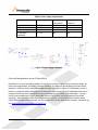
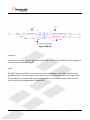
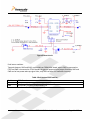
FRDM-KV31F Board User Manual FRDM-KV31F Rev. 0.00 Freescale Semiconductor Inc. Microcontroller Solutions Group Contents 1 Introduction ................................................................................................................................................3 FRDM-KV31F Hardware Overview.............................................................................................................................................. 3 2 FRDM-K31F hardware description .....................................................................................................5 Power supply .......................................................................................................................................................................................... 5 Serial and Debug Adapter version 2 (OpenSDAv2) .............................................................................................................. 6 Debug interface ..................................................................................................................................................................................... 7 Microcontroller...................................................................................................................................................................................... 8 Clock Source ............................................................................................................................................................................................ 9 Accelerometer and magnetometer............................................................................................................................................ 10 Thermistor ............................................................................................................................................................................................ 11 RGB LED ................................................................................................................................................................................................. 12 Serial port ............................................................................................................................................................................................. 13 Reset ........................................................................................................................................................................................................ 13 Push button switches ....................................................................................................................................................................... 14 Input/output connectors ............................................................................................................................................................... 15 Arduino compatibility ..................................................................................................................................................................... 16 3 References ................................................................................................................................................ 17 4 Revision history ...................................................................................................................................... 17 FRDM-KV31F User’s Manual Page 2 of 17 1 Introduction The Freescale Freedom development platform is a set of software and hardware tools for evaluation and development. It is ideal for rapid prototyping of microcontroller-based applications. The Freescale Freedom KV31 hardware, FRDM-KV31F, is a simple, yet sophisticated design featuring a Kinetis K series microcontroller, built on the ARM® Cortex®-M4 core - is a high-performance solution for BLDC, PMSM and ACIM motor control applications.. FRDM-KV31F can be used to evaluate the KV3x Kinetis K series devices. It features the MKV31F512VLL12 MCU, running at 100/120 MHz with DSP and floating point unit, it features dual 16-bit analog-to-digital converters (ADCs) sampling at up to 1.2 mega samples per second (MSPS), multiple motor control timers, 64 to 512 KB of flash memory and a comprehensive enablement suite from Freescale and its third-party resources including reference designs, software libraries and motor configuration tools. The FRDM-KV31F hardware is form-factor compatible with the ArduinoTM R3 pin layout, providing a broad range of expansion board options. The onboard interface includes a six-axis digital accelerometer & magnetometer, and a RGB LED. The FRDM-KV31F platform features OpenSDAv2, the Freescale open-source hardware embedded serial and debug adapter running an open-source bootloader. This circuit offers several options for serial communication, flash programming, and run-control debugging. OpenSDAv2 is an mbed™ HDKcompatible debug interface preloaded with the open-source CMSIS-DAP Interface firmware (mbed interface) for rapid prototyping and product development. FRDM-KV31F Hardware Overview The features of the FRDM-KV31F hardware are as follows: • MKV31F512VLL12 MCU (120 MHz with DSP instructions, 512 KB flash memory and 96 KB RAM , motor control timers, and 100 LQFP) Dual role USB interface with micro-B USB connector • RGB LED • FXOS8700CQ – accelerometer and magnetometer • Two user push buttons • Flexible power supply option – OpenSDAv2 USB, and external source • Easy access to MCU input/output through Arduino R3TM compatible I/O connectors • Programmable OpenSDAv2 debug circuit supporting the CMSIS-DAP Interface software that provides: o Mass storage device (MSD) flash programming interface o CMSIS-DAP debug interface over a driver-less USB HID connection providing runcontrol debugging and compatibility with IDE tools o Virtual serial port interface o Open-source CMSIS-DAP software project: github.com/mbedmicro/CMSIS-DAP. FRDM-KV31F User’s Manual Page 3 of 17 Figure 1 shows the block diagram of the FRDM-KV31F design. The primary components and their placement on the hardware assembly are explained in Figure 2. Figure 1 FRDM-KV31F platform Block Diagram FRDM-KV31F User’s Manual Page 4 of 17 Figure 2 FRDM-KV31F main components placement 2 FRDM-K31F hardware description Power supply There are multiple power supply options on the FRDM-KV31F board. It can be powered from the USB connectors, the VIN pin on the I/O header, DC Jack (not populated), or an offboard 1.71–3.6 V supply from the 3.3 V pin on the I/O header. The USB, DC jack, and VIN supplies are regulated onboard using a 3.3 V linear regulator to produce the main power supply. DC to DC linear regulator is not available in 3.3 V on J20 Header, however a direct supply to KV31 MCU is available. Table 1 provides the operational details and requirements for the power supplies. FRDM-KV31F User’s Manual Page 5 of 17 Table 1 Power supply requirements Supply source Valid range OpenSDAv2 USB VIN Pin 3.3V Header (J20) DC Jack (Not Populated) 5V 5–9V 1.71 – 3.6 V 5–9V OpenSDAv2 operational? Yes No No No Regulated onboard? Yes Yes No Yes Figure 3 Power Supply schematic Serial and Debug Adapter version 2 (OpenSDAv2) OpenSDAv2 is a serial and debug adapter circuit which includes an open-source hardware design, an open-source bootloader, and debug interface software. It bridges serial and debug communications between a USB host and an embedded target processor as shown in Figure 4. The hardware circuit is based on a Freescale Kinetis K20 family microcontroller (MCU) with 128 KB of embedded flash and an integrated USB controller. OpenSDAv2 comes preloaded with the CMSIS-DAP bootloader – an opensource mass storage device (MSD) bootloader and the CMSIS-DAP Interface firmware (aka mbed interface), which provides a MSD flash programming interface, a virtual serial port interface, and a CMSIS-DAP debug protocol interface. For more information on the OpenSDAv2 software, see mbed.org and https://github.com/mbedmicro/CMSIS-DAP FRDM-KV31F User’s Manual Page 6 of 17 Debug interface Signals with SPI and GPIO capability are used to connect directly to the SWD of KV31. These signals are also brought out to a standard 10-pin (0.05”) Cortex debug connector (J9). It is possible to isolate the KV31 MCU from the OpenSDAv2 circuit and use J9 to connect to an offboard MCU. To accomplish this, cut the trace on the bottom side of the PCB that connects J11 pin 2 to J9 pin 4. This will disconnect the SWD_CLK pin to the KV31 so that it will not interfere with the communications to an offboard MCU connected to J11. FRDM-KV31F User’s Manual Page 7 of 17 Figure 4 SWD Debug connecor J9 is populated by default. A mating cable, such as a Samtec FFSD IDC cable, can then be used to connect from the OpenSDAv2 of the FRDM-KV31F to an offboard SWD connector. Virtual serial port A serial port connection is available between the OpenSDAv2 MCU and pins PTA1 and PTA2 of the KV31 Microcontroller The FRDM-KV31F features the MKV31F512VLL12 MCU. The KV31 MCU family is a highly scalable member of the Kinetis V series and provides a high-performance, cost-competitive motor control solution. Built on the ARM®Cortex®-M4 core running at 120 MHz, combined with floating point and DSP capability, this is implemented in the 100pin LQFP package. The following table describes some of the features of the MKV31F512VLL12 MCU. Performance • 120 MHz ARM Cortex-M4 core with DSP instructions delivering 1.25 Dhrystone MIPS per MHz • Dual 16-bit ADCs sampling at up to 1.2 MS/s in 12-bit mode • 20 channels of highly flexible motor control timers (PWMs) across 4 independent time bases • Large RAM block enabling local execution of fast control loops at full clock FRDM-KV31F User’s Manual Page 8 of 17 Memories and memory interfaces System peripherals Clocks Security and integrity modules Analog modules Timers Communication interfaces speed • 512 KB of embedded flash and 96 KB of RAM • FlexBus external bus interface • Serial programming interface (EzPort) • Preprogrammed Kinetis flashloader for one-time, insystem factory programming • Flexible low-power modes, multiple wake-up sources • 16channel DMA controller • Independent external and software watchdog monitor • One crystal oscillator with two ranges: 32-40 kHz or 3-32 MHz • Three internal oscillators: 32 kHz, 4 MHz, and 48 MHz • Multipurpose clock generator with PLL and FLL • Hardware CRC module • 128-bit unique identification (ID) number per chip • Hardware random-number generator • Flash access control to protect proprietary software • Two 16-bit SAR ADCs (1.2 MS/s in 12bit mode) • Two 12bit DACs • Two analog comparators (CMP) with 6-bit DAC • Accurate internal voltage reference • Two 8-ch motor-control/general purpose/PWM timers • Two 2-ch motor-control/general purpose timers with quadrature decoder functionality • Periodic interrupt timers • 16-bit low-power timer • Programmable delay block • Two SPI modules • Three UART modules and one lowpower UART • Two I2C: Support for up to 1 Mbps operation Clock Source A 8MHz external crystal, is used for the external clock source of the KV31. Figure 5 Clock Source FRDM-KV31F User’s Manual Page 9 of 17 Accelerometer and magnetometer A Freescale FXOS8700CQ low-power, six-axis Xtrinsic sensor is interfaced through an I2C bus and two GPIO signals, as shown in Table 5. By default, the I2C address is 0x1D (SA0 pullup and SA1 pulldown). Table 2 Accelerometer and magnetometer signals connections FXOS8700CQ SCL SDA NT1 INT2 KV31 PTD2/LLWU_P13/SPI0_SOUT/UART2_RX/FTM3_CH2/FBA_AD4/LPUART0_RX/I2C0_SCL PTD3/SPI0_SIN/UART2_TX/FTM3_CH3/FBA_AD3/LPUART0_TX/I2C0_SDA PTD0/LLWU_P12/SPI0_PCS0/UART2_RTS/FTM3_CH0/FBA_ALE/FBA_CS1/FBA_TS/LPUART0_RTS PTC18/LPUART0_RTS/FBA_TBST/FBA_CS2/FBA_BE15_8_BLS23_16 FRDM-KV31F User’s Manual Page 10 of 17 Figure 6 Accelerometer and Magnetometer Thermistor There is a thermistors RT1 provided on the board that can be used as single ended or differential analog inputs to the KV31. In addition to the thermistor there is a resistor between the thermistor and 3.3V system power supply and another resistor between the thermistor and ground. The thermistor is a 10K ohm part but the associated divider chain uses different resistors. This makes the voltage across the thermistor larger or smaller and provides the ability to try the different gain settings on the analog channels. The FRDM-KV31F User’s Manual Page 11 of 17 thermistor circuit is designed to provide useable differential inputs over the temperature range of 90˚C to -20˚C. In addition to the thermistor voltage divider chain, the thermistor has a 0.1 uF capacitor in parallel. Each analog input to the KV31 has a 100 ohm series resistor and a 2200pF capacitor as a low pass filter. This helps protect the KV31 from electrostatic discharges and lowers the impedance of the analog signal so that it can be sampled with less noise. Figure 7 Thermistor RGB LED RGB LED is connected through GPIO, signal connections are shown in Table. Table 3 LED Signal connections RGB LED RED BLUE GREEN KV31 PTD1/ADC0_SE5B/SPI0_SCK/UART2_CTS/FTM3_CH1/FBA_CS0/LPUART0_CTS PTE25/ADC0_SE18/FTM0_CH1/I2C0_SDA/EWM_IN TD7/UART0_TX/FTM0_CH7/FTM0_FLT1/SPI1_SIN FRDM-KV31F User’s Manual Page 12 of 17 Figure 8 RGB LED Serial port The primary serial port interface signals are PTB16 UART0_RX and PTB17 UART0_TX. These signals are connected to the OpenSDAv2 circuit. Reset The RESET signal on the K20 is connected externally to a pushbutton, named SW1, and also to the OpenSDAv2 circuit. The reset button can be used to force an external reset event on the target MCU. The reset button can also be used to force the OpenSDAv2 circuit into boot loader mode. For more details, see Serial and debug adapter (OpenSDAv2). FRDM-KV31F User’s Manual Page 13 of 17 Figure 9 Reset circuit Push button switches Two push buttons, SW2 and SW3, are available on FRDM-K64F board, where SW2 is connected to PTC6 and SW3 is connected to PTA4. Besides the general purpose input/output functions, SW2 and SW3 can be low-power wake up signal. Also, only SW3 can be a non-maskable interrupt. Table 4 Push button GPIO function Switch SW2 SW3 GPIO Function PTA4/LLWU_P3/FTM0_CH1/FTM0_FLT3/NMI/EZP_CS PTE4/LLWU_P2/SPI1_PCS0/LPUART0_TX FRDM-KV31F User’s Manual Page 14 of 17 Figure 10 Pushbutton switches Input/output connectors The MKV31F512VLL12 microcontroller is packaged in a 100-pin LQFP. Some pins are utilized in onboard circuitry, but some are directly connected to one of the four I/O headers. The pins on the KV31 microcontroller are named for their general purpose input/output port pin function. For example, the first pin on Port A is referred as PTA1. The name assigned to the I/O connector pin is same as of the KV31 pin connected to it, if applicable. FRDM-KV31F User’s Manual Page 15 of 17 Figure 11 IO header pinout Arduino compatibility The I/O headers on the FRDM-KV31F board are arranged to enable compatibility with peripheral boards (known as shields) that connect to Arduino and Arduino-compatible microcontroller boards. The outer rows of pins (even numbered pins) on the headers, share the same mechanical spacing and placement with the I/O headers on the Arduino Revision 3 (R3) standard. FRDM-KV31F User’s Manual Page 16 of 17 3 References The following references are available on freescale.com : • FRDMKV31FQSG, FRDM-KV31F Quick Start Guide • FRDM-KV31F Pinouts • FRDM-KV31F Schematic • FRDM-KV31F Design Package 4 Revision history Revision number 0 Date 06/2015 FRDM-KV31F User’s Manual Substantial changes Initial release Page 17 of 17