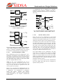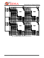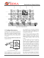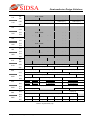
1
SIDSA
Chapter 2
FIPSOC Programmable Logic
FIPSOC
User’s Manual
SIDSA
Semiconductor Design Solutions
FIPSOC Programmable Logic
Overview
The Field Programmable System On Chip (FIPSOC)
constitutes a new concept in system integration. It
provides the user with the possibility of integrating a
microprocessor core along with programmable digital
and analog cells within the same integrated circuit.
This chip can be considered as a large granularity
FPGA with a FPAA (Field Programmable Analog
Array) and a built-in microprocessor core that does
not only act as a general purpose processing element,
but also configures the programmable cells and their
interconnections. Therefore, there is a strong
interaction between hardware and software as long as
signal values and configuration data within the
programmable
cells
are
accessible
from
microprocessor programs.
This manual describes the FPGA included in the
chip. It is composed of an array of DMCs (Digital
Macro Cells) surrounded by IOBs (In/Out Blocks)
and IICs (Internal Interface Cells). The DMC is the
basic tile repeated to form the FPGA core. The IOBs
are the programmable IO cells that include bonding
pads to communicate with the external world. The
IICs are special ports to interconnect the
microprocessor and the routing channels of the
FPGA.
Figure 1.1 shows an overview of a generic MxN
FPGA. In later sections each of these elements
(DMCs, IOBs and IICs) are described separately.
DMCs and other FPGA elements are designated
vertically from bottom to top with numbers (zero is
the first one), and horizontally form right to left with
capital letters (‘A’ is the first one). Therefore, the
DMC located at the bottom right corner is designated
as (0,A).
Chapter 2. FIPSOC Programmable Logic
1. Digital Macro Cell (DMC)
This section describes the functionality of the Digital
Macro Cell (DMC), the programmable digital
element of the FPGA. It is a large granularity, 4-bit
wide, LUT-based programmable cell with
combinational and sequential resources. It easily
interfaces the microprocessor through the memory
space, and can be dynamically reconfigured while in
operation as far as two operating contexts are stored
at every moment.
In the static modes (that is, not in the dynamically
reconfigurable modes), the combinational part of the
DMC includes four 16-bit Look Up Tables (LUTs)
that can be programmed to carry out any function of
4 inputs. Each two LUTs constitute a tile and share
two inputs. These two-LUTs in each tile can be
grouped to carry out any 5-input boolean function,
and the four LUTs can be connected to implement a
single 6-input function. Each combinational tile can
also be configured to perform a multiplexing function
of two custom functions, in particular as a 4 to 1
multiplexer.
In the dynamically reconfigurable modes, the DMC
has four 8-bit independent LUTs that share no inputs,
each of which can implement any 3-input function.
As before, two LUTs can carry out a 4-input function
and the whole combinational block can implement
any 5-input boolean function. In these modes, two
independent contexts are stored in RAM bits, so there
are two backup copies of each configuration bit but
for the LUTs. The contexts can be independently read
and written, while only one of them can be active.
This means that one of the contexts can be changed
while the device is operating within the other context,
and once it is configured then it can be activated to
suddenly change the functionality of the device
without even affecting its operation. The main allure
of this approach is that it is not necessary to stop the
device to reconfigure it.
2
SIDSA
Semiconductor Design Solutions
Fig 1.1: The FIPSOC FPGA Structure (overview)
The combinational part of the DMC can also be
configured as a 4-input adder with carry-in and carryout. This adder can be expanded connecting more
DMCs to the carry pins, and fits in one context (that
is, the DMC can be used as an adder in one context
and as general purpose LUTs in the other one).
Finally, each tile (that is, every two LUTs) can be
used as a stackable RAM memory block (16x2 RAM
in the normal modes, 8x2 RAM in each context in the
dynamic modes).
The sequential part of the DMC is also 4-bit wide. It
includes four flip-flops than can be individually
configured as D-type with enable, mux-type, and 4bit macro functions. Each FF can be individually
configured with normal or negated output, and each
of the two reset mechanisms (global and local) can be
individually selected as reset or set. The global reset
is always asynchronous, while the local reset can be
selected to be synchronous or asynchronous for the
four of them (not individually). The clock polarity
and a latch/FF mode can also be set for the four FFs.
The 4-bit macro functions provide an optimized way
to implement 4-bit up/down counters with load and
enable, and 4-bit shift registers with load and enable.
These functions may be expanded to any number of
bits by connecting more DMCs to the carry pins.
Chapter 2. FIPSOC Programmable Logic
The microprocessor can also read from and write data
into the FFs. As in the combinational block, two
contexts are also available for the configuration of the
sequential block. The user can write one of them
while the other one is active so the dynamic
reconfiguration can take place without interruption of
operation. Furthermore, the data into the FFs can also
be stored with the rest of the context and then
restored back upon context swap.
Finally, there are some routing resources to flexibly
interconnect the combinational and sequential parts
of the DMC. Both parts can be used more or less
independently, although a limited number of output
pins are available. See next section for details.
The dynamically reconfigurable mode can be selected
for any combination of DMCs. Also, the hardware
swap can be triggered for a group of DMCs rather
than for the whole chip.
1.1.
Block Diagram and I/O Pins.
A simplified block diagram of the DMC can be seen
in fig. 1.2.
3
SIDSA
OAUX1
Semiconductor Design Solutions
OAUX2
GOE
COUTC C1 C2
GOE
COUTS C3 S1 S2
COUTC
IA5
IA4
IA3
IA2
IA1
IA0
IB5
IB4
IB3
IB2
IB1
IB0
COUTS
C3
D3
Comb.
Block
C2
D2
C1
Internal
Router
D1
C0
D0
R7
R6
R5
R4
R3
R2
R1
R0
Seq.
Block
OE1
OE0
IAUX1
IAUX2
CLK
E
LSR
GSRN
D3 D2 D1 D0
S3
C3
O3
S2
C2
O2
S1
C1
OE1
GOE
O1
S0
C0
O0
OE0
GOE
Fig 1.2: Block Diagram of the Digital Macro Cell (DMC)
1.1.1. I/O signals
The signals marked with arrows are global I/O pins
for each DMC. All of them are described hereby:
IA5-IA0, IB5-IB0: These are the input pins for the
LUTs. In the static modes, IA3 and IA2 are shared by
the first couple of 4-input LUTs (See Section 1.2:
Combinational Block), and also are IB3 and IB2 (by
the two LUTs of the lower tile). In the dynamic
modes, no inputs are shared as far as there are four 3input LUTs. These pins are also used as data inputs in
the 4-bit adder mode and as address and control pins
in the memory modes.
IAUX1: The first auxiliary signal IAUX1 is used for
extra input in the sequential macro modes. In the
counter mode (sequential part), IAUX1 is the
up/down control pin (up on high level). In the shift
register (SHR) mode, IAUX1 is the enable control
pin (active high).
IAUX2: The second auxiliary signal IAUX2 is used
for extra input in the sequential macro modes. In the
counter mode, it is the carry-in signal. In the shift
register (SHR) mode, it is the input pin for the
incoming bit stream.
D3-D0: The data inputs D3-D0 are mainly used as
direct inputs for the sequential part. They provide a
neat way to independently use the combinational and
sequential parts of the DMC. They are also used as
the input data bus in the memory modes. It should be
noted that both the combinational outputs (C3-C0 in
the diagram) and the direct inputs (D3-D0) are used
in the mux-type FF modes, and their detailed routing
is determined by the configuration of the internal
outer block (see section 5 Routing Resources).
CLK: This is the clock input. Its polarity can be
configured as rising or falling edge (FF modes), or
high or low level (Latch modes). This terminal is the
same for each of the four FFs.
E: The Enable pin is used as the enable input (active
high) for the D-type with enable FF mode. In the
Chapter 2. FIPSOC Programmable Logic
4
SIDSA
mux-type FF mode, the E pin is used as the selection
pin (a high level on the E pin selects the D input, a
low level selects the D2 input in each FF, See Section
1.3: Sequential Block). In the counter mode, the E
input is the load control pin (a low level loads data
into the counter). In the shift register (SHR) mode,
the E input is the load control pin (a high level loads
a parallel word into the register). This terminal is the
same for the four FFs, although there is an special
mode which provides a local enable capability (see
Section 1.3: Sequential Block).
LSR: This is the Local Set/Reset input for the FFs. It
can be configured for synchronous or asynchronous
operation (same for the four FFs), and to reset or set
each FF (this is configured individually for each FF).
This pin is active high and is shared by the four FFs.
However, there is still an alternative mode which
provides local synchronous reset capability (but not
set).
GSRN: This is the asynchronous Global Set/Reset
input for the FFs. It can be configured for reset or set
operation (this is configured individually for each
FF). This pin is active low and is shared by the four
FFs.
OAUX1: The first auxiliary output is mainly used to
drive the carry out from the combinational block in
the adder mode out of the DMC. It also can route
other combinational and sequential outputs (See
section 1.4: Internal Routing Resources).
OAUX2: The second auxiliary output is mainly used
to drive out of the DMC the carry out from the
sequential block in the counter mode and the output
bit stream in the shift register (SHR) mode. It also
can route other combinational and sequential outputs
(See section 1.4: Internal Routing Resources).
1.1.2. Internal signals
The names given to the internal signals generated at
the interfaces between the different blocks described
in the block diagram (figure 1.2) are the following:
GOE: This input is connected to the Global Output
Enable net (this terminal is shortcut to the GOE
terminal of every DMC and every IOB of the chip). It
can be used during startup to disable every output pin
on every DMC and every IOB to avoid random
output collisions.
C3-C0: These are the outputs of the combinational
block. They are generated by the LUTs and their
internal connectivity depends on the operating mode
(See Section 1.2: Combinational Block). In the
memory mode, they are the output data bus. In the
adder mode, they drive the result of the addition
R7-R0: These are the outputs of the router block. The
router block simply interchanges its inputs, so R7-R0
are the same than C3-C0 and D3-D0 but not in the
Chapter 2. FIPSOC Programmable Logic
Semiconductor Design Solutions
same order. In fact, R7-R4 can only map to some
permutations of C3, D3, C2 and D2 (that is, signals
related to the upper tile), and the same applies to R3R0 with C1, D1, C0 and D0 (lower tile). Refer to
section 1.4: Internal Routing Resources for details.
S3-S0: These are the outputs of the sequential blocks.
OE1, OE0: These signals are the control pins for the
tri-state output buffers. As it can be seen in figures
1.8 and 1.14, the output control signals OE1 and OE0
are the or function of the CCO configuration bit and
IA0 and IB0 respectively for each tile. This
configuration bit should only be used to control the
output buffers when building larger memories,
although it can be used at any moment. When the tile
is configured in memory mode, OE1 is the output
enable signal for the upper 16x2 memory tile, and
OE0 is the same for the lower tile. The memory
output is then enabled only when the chip select line
is high (IA0 for the upper tile, IB0 for the lower tile)
and the output control option is enabled
(configuration bit CCO reset to zero).
COUTC: This is the carry-out signal from the
combinational part when it is configured as a 4-bit
adder. There is a fast dedicated connection to drive
this signal to the carry-in input of the upper DMC.
COUTS: This is the carry-out signal from the
sequential part when it is configured as an up-down
counter. It also drives the output bit stream in the
shift register (SHR) mode. There is a fast dedicated
connection to drive this signal to the carry-in (or bitstream in) input of the upper DMC.
1.1.3. Configuration Data
The configuration data is stored in RAM bits that in
fact are duplicated to store two different contexts.
Configuration bits starting with CC correspond to the
combinational block, those with the prefix CR are
used for the routing resources, and the CS prefix
corresponds to the configuration bits of the sequential
block. For the combinational block, configuration bits
ending with 1 refer to the upper tile, 0 for the lower
one.
CCMA1, CCMB1 (upper tile); CCMA0, CCMB0
(lower tile): These bits select the operating mode for
the each tile as described in table 1.1:
CCMA1,
CCMA0
0
0
1
1
CCMB1,
CCMB0
0
1
0
1
Operating Mode
Simple Combinational
Multiplexer
Memory
Complex Combinational
Table 1.1: Operating modes of LUT pairs
CCMA1 and CCMB1 configure the upper tile, while
CCMA0 and CCMB0 configure the lower tile.
5
SIDSA
CCR: This bit activates the dynamic mode for the
combinational part of a DMC. If this bits is set, the
hardware swap command can be issued.
CCA: This bit configures the combinational block as
a 4-bit adder. CCMAx and CCMBx must be set to
zero to use the combinational block as a 4-bit adder.
CCO: When reset to zero, this bit provides user
control over the output buffers. As it can be seen in
figures 1.8 and 1.14, the output control signals OE1
and OE0 are the or function of this bits and IA0 and
IB0 respectively for each tile. This configuration bit
should only be used to control the output buffers
when building larger memories, although they can be
used at any moment. For normal operation (output
buffers always enabled), this bit must be set to one.
CR5-CR0: These bits configure the internal router
that connects the combinational block to the
sequential part of the DMC (See section 1.4: Internal
Routing Resources for details).
CR6-CR9: These bits configure the multiplexers for
the auxiliary output signals OAUX1 and OAUX2
(See section 1.4: Internal Routing Resources for
details).
CRO3-CRO0: These four bits configure the output
multiplexers to selectively drive through the output
pins O3-O0 the output signals from the
combinational or sequential part of the DMC (See
section 1.4: Internal Routing Resources for details).
CS1: The CS1 bit enables the 4-bit macro modes for
the sequential part of the DMC when set to zero. If
set to one, the four FFs are configured independently
through the CS2 and CS3 configuration bits (one per
FF).
CS2-CS3: They store the operating mode of each FF
in the sequential part of the DMC (See Section 1.3:
Sequential Block for details).
CS4: One per FF, it sets as reset (CS4=0) or set
(CS4=1) the GSRN signal.
CS5: One per FF, it sets as reset (CS5=0) or set
(CS5=1) the LSR signal.
Semiconductor Design Solutions
CSR: The CSR bit marks, when set, the sequential
part of the DMC as dynamically reconfigurable. This
means that the data in the FFs will be saved upon
context swap and restored when the saved context
becomes active again. When this bit is reset to zero,
the configuration context is swapped, but the actual
data in the FFs is not changed.
I: This bit stores the context ID currently set as active
for each DMC. It selects which part of the LUT is
active and which context of the FFs is being used. It
only has meaning when the CSR or CCR bits are set.
1.2.
Combinational Block
The combinational block is composed of two 6-input,
2-output tiles that can be independently configured,
except for the 4-bit adder mode. Each tile can be
configured in one of the four operating modes: simple
combinational, complex combinational, multiplexer
and memory mode. The two tiles are equivalent
except in the complex combinational mode.
Therefore, there are 17 static operating modes for the
combinational part of the DMC (two tiles, four
modes per tile plus the 4-bit adder mode). In the same
manner, there are 17 dynamic operating modes.
1.2.1. Static Operating Modes
To configure the upper tile in a static mode, the CCR
bit must be reset to zero. This is the only difference
between the configuration of any static mode and its
dynamically reconfigurable counterpart. Each
combinational tile can be independently configured in
a static or dynamically reconfigurable mode
(configuration bit CCR)
1.2.1.1.
Simple Static Combinational Mode:
In this mode, the tile performs two independent 4input combinational functions sharing 2 of them, as
depicted in figure 1.3. In this figure, both tiles are
configured in this Simple Static Combinational
Mode, although they do not have necessarily to be
configured in the same mode:
CS6: One per DMC, it sets as synchronous (CS6=0)
or asynchronous (CS6=1) the LSR reset/set signal.
CS7: One per DMC, it sets them as latch (CS7=0) or
FF (CS7=1).
CS8: One per DMC, it sets the clock polarity (CS8=0
for rising edge FF and low level sensitive latch,
CS8=1 for falling edge FF and high level sensitive
latch).
CS9: One per FF, it sets the polarity of the output
signals of the FFs (CS9=0 for Q, CS9=1 for negated
Q).
Chapter 2. FIPSOC Programmable Logic
6
SIDSA
IA5
IA4
IA3
4 LUT
C3
Semiconductor Design Solutions
IA5
IA4
IA3
IA2
IA1
C3
5-LUT
C2
IA2
IA1
IA0
IB5
IB4
IB3
4 LUT
4 LUT
C2
C1
IA0
IB5
IB4
IB3
IB2
IB1
C1
5-LUT
C0
IB0
IB2
IB1
IB0
4 LUT
C0
Fig 1.3: Simple Static Combinational Mode
(CCMA1=CCMB1=0, CCMA0=CCMB0=0, CCR=0)
For the Simple Static Combinational Mode the
configuration data is CCMA1=0 and CCMB1=0 for
the upper tile, and CCMA0=0 and CCMB0=0 for the
lower tile. CCR must also be 0.
1.2.1.2.
Complex Static Combinational
Modes:
The Complex Static Combinational Mode is different
for each tile. In fact, we will explain the three
possible combinations of static modes as long as the
functionality of a tile in the Complex Static
Combinational Mode depends on whether the other
tile is configured in the Simple or Complex Static
Combinational Mode. The common feature of this
mode for both tiles is that a 5-input function is carried
out by one of the outputs.
In figure 1.4 it can be seen both tiles configured in
the Complex Static Combinational Mode. C3 and C1
carry out two independent 5-input combinational
functions, while C2 multiplexes these outputs (IA0
controls the multiplexer, transmitting the upper
function when IA0=1 and the lower when IA0=0)
and C0 performs an AND function of these outputs
and the IB0 input. This mode correspond to
CCMA1=CCMA0=1, CCMB1=CCMB0=1, and
CCR=0.
Chapter 2. FIPSOC Programmable Logic
Fig 1.4: Static Complex Combinational Mode
(CCMA1=CCMA0=1, CCMB1=CCMB0=1, CCR=0)
The mixed modes (one tile in the Complex mode and
the other one in the Simple mode) are depicted in
figures 1.5 and 1.6. The configuration data is
CCMA1=CCMB1=1 and CCMA0=CCMB0=0 to
have the upper tile in the Complex mode and the
lower tile in the Simple mode (Fig. 1.5), and
CCMA1=CCMB1=0 and CCMA0=CCMB0=1 for
the upper tile to be in the Simple mode and the lower
tile in the Complex mode (Fig. 1.6). Both tiles are in
static modes (CCR =0) in both figures:
IA5
IA4
IA3
IA2
IA1
5-LUT
C3
C2
IA0
IB5
IB4
IB3
IB2
IB1
IB0
4 LUT
C1
4 LUT
C0
Fig 1.5: Upper Complex - Lower Simple Static Combinational
Mode (CCMA1=CCMB1=1, CCMBA0=CCMB0=0, CCR=0)
7
SIDSA
1.2.1.4.
IA5
IA4
IA3
IA2
IA1
IA0
IB5
IB4
IB3
IB2
IB1
4 LUT
C3
4 LUT
C2
5-LUT
C1
C0
IB0
Fig 1.6: Upper Simple - Lower Complex Static Combinational
Mode (CCMA1=CCMB1=0, CCMBA0=CCMB0=1, CCR=0)
1.2.1.3.
Static Multiplexer Mode:
Each combinational tile can be configured as a 4 to 1
multiplexer. The behavior of the whole tile is like in
the complex combinational mode, but performing the
multiplexing function instead of the custom complex
one.
(Note: In fact, each combinational tile can be configured to
perform a multiplexing function of the two simple custom
functions of the simple mode. This usage is tricky and will
be explained in the next release of this user manual)
In Fig. 1.7 it is shown the combinational part of a
DMC in which both tiles are configured as static 4 to
1 multiplexers. All combinations of multiplexer
modes and simple, complex and memory
configurations apply, and can be derived from the
wiring described in the complex combinational
modes section.
A combinational tile is configured as an static
multiplexer when CCMA=0, CCMB=1 and CCR=0.
Special configuration data has also to be loaded into
the LUTs
C3
S1
The address pins are IA1-IA4 for the upper tile (IB1IB4 for the lower tile). The chip select line is IA0 for
the upper tile (IB0 for the lower tile), and it is active
high (select on high level). The read/write line is IA5
for the upper tile (IB5 for the lower tile), and it is
active high (read on high level, write on low level).
The input data bus is D3-D2 for the upper tile and
D1-D0 for the lower tile.
The output buffers can be controlled by the chip
select lines if the output control option is enabled
(CCO set to low). If this bit is set to high, the output
buffers are always enabled. If set to low, the output
buffers are enabled when the chip select lines (inputs
IA0 and IB0) are active. With this technique, one can
build larger memory blocks.
In figure 1.8 it can be observed the combinational
part of the DMC when both tiles are configured as
memory blocks.
IA4
IA3
IA2
IA1
a3
a2
a1
a0
IA5
__
R/W
IA0
CS
16x2
RAM
Dout1 C3
Dout2 C2
Din1 Din0
D3
IB4
IB3
IB2
IB1
a3
a2
a1
a0
IB5
__
R/W
CS
D2
CCO
IA0
OE1
CCO
IB0
OE0
16x2
RAM
Dout1
Dout2
C1
C0
Din1 Din0
D1
D0
S0
A3
A2
A1
A0
Y
C2
S1
S0
A3
A2
A1
A0
C1
Y
C0
Fig 1.7: Static Multiplexer Combinational Mode (both tiles)
(CCMA1=CCMA0=0, CCMB1=CCMB0=1, CCR=0)
Chapter 2. FIPSOC Programmable Logic
Fig 1.8: Static Memory Mode (both tiles)
(CCMA1=CCMA0=1, CCMB1=CCMB0=0, CCR=0)
All combinations of the memory mode and simple,
complex and multiplexer configurations apply, and
can be derived from the wiring described in the
complex combinational modes section.
IB5
IB2
IB4
IB3
IB1
IB0
Static Memory mode:
Each 2-bit tile can be configured as a 16x2 RAM
memory. Here the words static and dynamic do not
mean static and dynamic RAM types as it is normally
understood, but they apply to the configuration type.
IB0
IA5
IA2
IA4
IA3
IA1
IA0
Semiconductor Design Solutions
As it can be seen, when both tiles are used to
implement a 16x4 RAM memory, all of the inputs to
the DMC are not used and therefore the sequential
part may only be used in a macro mode (shift
register, counter) or to latch or clock the data out of
the RAM.
8
SIDSA
To configure the upper tile in the Static Memory
Mode, CCMA1 must be set to 1, CCMB1 must be set
to zero and CCR must be set to zero (CCMA0=1,
CCMB0=0 for the lower tile)
1.2.2. Dynamic Operating Modes
The dynamically reconfigurable modes are used to
implement the hardware swap. In these modes, two
contexts are stored for the combinational part of the
DMC, so in fact there are two virtual DMCs while
only one of them is active. The non-active context
can be rewritten while the other one is active, and the
active and non-active contexts can be swapped
without affecting the device operation.
To select the combinational part of the DMC as
dynamically reconfigurable, CCR should be set to
one.
As explained in section 4 “Configuration Memory”
of this manual, the context load operation can be
triggered either by a microprocessor write or by the
combinational part of a DMC. Configuration bit
CHWR sets the DMC into a special mode for
triggering context loads: when this bit is set, input
pins IA2 and IB2 are used in the place of IA3 and
IB3. IA3 is used then to actually trigger the context
load process for the DMC when a high level is
applied, while IB3 is used to select which context is
to be transferred (low level for context #0, high level
for context #1). Therefore, in the dynamic simple
combinational mode each two LUTs would share an
input pin (IA2 instead of IA3 for the upper tile, IB2
instead of IB3 for the lower) if CHWR is set, and the
dynamic multiplexer mode would only have three
different inputs (IA2 and IB2 instead of IA3 and IB3)
1.2.2.1.
Dynamic Simple Combinational
Mode:
In this mode, the tile performs two independent 3input combinational functions sharing none of them,
as depicted in figure 1.9. In this figure, both tiles are
configured in this Simple Dynamic Combinational
Mode.
IA5
IA4
IA3
3 LUT
C3
IA2
IA1
IA0
3 LUT
C2
IB5
IB4
IB3
3 LUT
C1
IB2
IB1
IB0
3 LUT
C0
Semiconductor Design Solutions
For the Simple Dynamic Combinational Mode the
configuration data is CCMA1=CCMB1=0 and
CCR=1 for the upper tile, and CCMA0=CCMB0=0
and CCR=1 for the lower tile. As long as it is a
dynamic mode, two contexts are stored.
1.2.2.2.
Complex Dynamic Combinational
Modes:
The Complex Dynamic Combinational Mode is
different for each tile. In fact, we will explain the
three possible combinations of Complex dynamic
modes as long as the functionality of a tile in the
Complex Combinational Mode depends on whether
the other tile is configured in the Simple or Complex
Combinational Mode. The common feature of this
mode for both tiles is that a 4-input function is carried
out by one of the outputs.
In figure 1.10 it can be seen both tiles configured in
the Complex Dynamic Combinational Mode. C3 and
C1 carry out two independent 4-input combinational
functions, while C2 multiplexes these outputs (IA0
controls the multiplexer, transmitting the upper
function when IA0=1 and the lower when IA0=0)
and C0 performs an AND function of these outputs
and the IB0 input. This mode correspond to CCR=1
with CCMA1=CCMA0=1, CCMB1=CCMB0=1.
IA5
IA4
IA2
IA1
4-LUT
C3
C2
IA0
IB5
IB4
IB2
IB1
4-LUT
C1
C0
IB0
Fig 1.10: Dynamic Complex Combinational Mode
(CCMA1=CCMA0=1, CCMB1=CCMB0=1, CCR=1)
The dynamic mixed modes (one tile in Complex
mode and the other one in Simple mode) are depicted
in figures 1.11 and 1.12. The configuration data is
CCMA1=CCMB1=1 and CCMA0=CCMB0=0 to
have the upper tile in Complex mode and the lower
tile in Simple mode (Fig. 1.11), and
CCMA1=CCMB1=0 and CCMA0=CCMB0=1 the
other way round (Fig. 1.12). In these figures, DMCs
are configured as dynamically reconfigurable
(CCR=1):
Fig 1.9: Simple Dynamic Combinational Mode
(CCMA1=CCMB1=0, CCMA0=CCMB0=0, CCR=1)
Chapter 2. FIPSOC Programmable Logic
9
SIDSA
IA5
IA4
IA2
IA1
4-LUT
Semiconductor Design Solutions
A combinational tile is configured as a dynamic
multiplexer when CCMA=0, CCMB=1 and CCR=1.
Special configuration data has also to be loaded into
the LUTs
C3
C2
IA5
IA1
IA0
IB5
IB4
IB3
IB2
IB1
IB0
3 LUT
3 LUT
C1
IA2
IA1
IA0
IB5
IB4
IB2
IB1
A3
A2
A1
A0
Y
C2
S1
IB4
IB3
IB2
IB0
S0
A3
A2
A1
A0
C1
Y
C0
Fig 1.13: Dynamic Multiplexer Combinational Mode (both
tiles) (CCMA1=CCMA0=0, CCMB1=CCMB0=1, CCR=1)
3 LUT
C3
3 LUT
C2
1.2.2.4.
4-LUT
Dynamic Memory mode:
Each 2-bit tile can be configured as a 8x2 RAM
memory. Here the words static and dynamic do not
mean static and dynamic RAM types as it is normally
understood, but they apply to the configuration type.
C1
C0
IB0
Fig 1.12: Upper Simple - Lower Complex Static Combinational
Mode (CCMA1=CCMB1=0, CCMA0=CCMB0=1, CCR=1)
Finally, it should be remembered that two contexts
are stored for each dynamically reconfigurable tile.
1.2.2.3.
S0
IB5
IB1
C0
Fig 1.11: Upper Complex - Lower Simple Dynamic
Combinational Mode (CCMA1=CCMB1=1,
CCMA0=CCMB0=0, CCR=1)
IA5
IA4
IA3
C3
S1
IA4
IA3
IA2
IA0
Dynamic Multiplexer Mode:
Each combinational tile can be configured as a 4 to 1
multiplexer. The behavior of the whole tile is like in
the complex combinational mode, but performing the
multiplexing function instead of the custom complex
one. This mode works exactly as in the static mode,
but with a slightly different wiring.
(Note: In fact, each combinational tile can be
configured to perform a multiplexing function of the
two simple custom functions of the simple mode. This
usage is tricky and will be explained in the next
release of this user manual)
The address pins are IA4, IA2 and IA1 for the upper
tile (IB4, IB2 and IB1 for the lower tile). The chip
select line is IA0 for the upper tile (IB0 for the lower
tile), and it is active high (select on high level). The
read/write line is IA5 for the upper tile (IB5 for the
lower tile), and it is active high (read on high level,
write on low level). The input data bus is D3-D2 for
the upper tile and D1-D0 for the lower tile.
The output buffers can be controlled by the chip
select lines if the output control option is enabled
(CCO set to low). If this bit is set to high, the output
buffers are always enabled. If set to low, the output
buffers are enabled when the chip select lines (inputs
IA0 and IB0) are active. With this technique, one can
build larger memory blocks.
In figure 1.14 it can be observed the combinational
part of the DMC when both tiles are configured as
dynamic memory blocks.
In Fig. 1.13 it is shown the combinational part of a
DMC in which both tiles are configured as static 4 to
1 multiplexers. All combinations of multiplexer
modes and simple, complex and memory
configurations apply, and can be derived from the
wiring described in the complex combinational
modes section.
Chapter 2. FIPSOC Programmable Logic
10
SIDSA
IA4
IA2
IA1
a2
a1
a0
IA5
R/W
IA0
CS
8x2
RAM
__
C3
Dout1
C2
Dout2
Din1 Din0
D3
IB4
IB2
IB1
a2
a1
a0
IB5
R/W
IB0
CS
D2
CCO
IA0
OE1
CCO
IB0
OE0
8x2
RAM
__
C1
Dout1
C0
Dout2
Din1 Din0
D1
D0
Semiconductor Design Solutions
The carry-out signal can be routed through the
OAUX1 output pin. The block has exactly the same
pin-out regardless of the status of the CCR bits,
although in the dynamic mode IA3 and IA2 (IB3 and
IB2 for the lower tile) would have to be explicitly
tied together, and the number or arithmetic functions
supported in dynamic mode is smaller. To configure
the combinational part of the DMC in the 4-bit
arithmetic mode, the CCA bit has to be set to one and
the CCMAx and CCMBx bits have to be set to zero.
Appropriate data has to be loaded into the LUTs for
the required arithmetic operation (adder, substractor,
etc)
1.2.4. Configuration table
Fig 1.14: Dynamic Memory Mode (both tiles)
(CCMA1=CCMA1=1, CCMB1=CCMB0=0, CCR=1)
All combinations of the memory mode and simple,
complex and multiplexer configurations apply, and
can be derived from the wiring described in the
complex combinational modes section.
As it can be seen, when both tiles are used to
implement a 8x4 RAM memory, all of the inputs to
the DMC are not used (except the auxiliary inputs
IAUX1 and IAUX2) and therefore the sequential part
could only be used in a macro mode (shift register,
counter) or to latch or clock the data out of the RAM.
In this dynamic mode, two contexts are stored for
each tile. This means that a 8x2 RAM memory block
can exist as a virtual hardware block keeping the data
previously written when the context was active.
To configure the upper tile in the Dynamic Memory
Mode, CCMA1 must be set to 1, CCMB1 must be set
to zero and CCR must be set to one (CCMA0=1,
CCMB0=0 for the lower tile)
1.2.3. 4-bit Arithmetic Mode
This mode is set globally for the whole combinational
part of the DMC. The input words are, from MSB to
LSB, [IA5_IA1_IB5_IB1] and [IA4_IA0_IB4_IB0].
The carry-in signal is the IB2 pin. In figure 1.15 it
can be found a sketch of the 4-bit arithmetic mode.
We include hereby a reference table (table 1.2) to
help the user configure a combinational tile. For an
upper tile, the ‘x’ in the following table should be a
‘1’. For the lower tile, a ‘0’.
Configuration
STATIC
DYNAMIC
4-BIT ADDER
CCR
0
0
0
0
1
1
1
1
CCMAx
CCMBx
Mode
0
0
Simple
0
1
Mux
1
0
RAM
1
1
Complex
0
0
Simple
0
1
Mux
1
0
RAM
1
1
Complex
CCA=1, CCMAx= CCMBx=0
Table 1.2: Combinational tile operating modes
1.3.
Sequential Block
The sequential block has been designed to have a
convenient and flexible interface to the combinational
part. It is 4-bit wide as well and supplies the user with
several FF types to be used more or less
independently.
A general block diagram can be seen in figure 1.16.
As it can be observed, each FF has two data inputs,
an enable pin, two resets, the clock input and the Q
output.
COUTC
IA5
IA1
IB5
IB1
IA4
IA0
IB4
IB0
a3
a2
a1
a0
Cout
S=f(a,b)
b3
b2
b1
b0
S3
S2
S1
S0
C3
C2
C1
C0
Cin
IB2
Fig 1.15: 4-bit Arithmetic Mode
(CCMA1=CCMA0=CCMB1=CCMB0=0, CCA=1).
Chapter 2. FIPSOC Programmable Logic
11
SIDSA
Semiconductor Design Solutions
1.3.1. I/O and control signals
R7
R6
E
D
D2
S3
Q
CLK
LSR
R5
R4
GSRN
E
D
D2
S2
Q
The shared signals for all FFs are CLK, E, LSR and
GSRN:
CLK
LSR
R3
R2
GSRN
E
D
D2
S1
Q
CLK
LSR
R1
R0
GSRN
E
D
D2
S0
Q
CLK
LSR
The sequential part of the DMC is composed of four
FFs which share their control signals but not their
data pins. Control signals and data pins have different
functions depending on the operating mode in which
an individual FF is configured (this will be explained
in detail in next paragraph). We describe hereby the
common features for all the operating modes and the
common control signals.
GSRN
Fig 1.16: Sequential Block Overview.
The FF blocks can be configured more or less
independently as described in paragraph 1.17. All the
configuration bits used for the sequential part of the
DMC are in fact duplicated to store two contexts and
therefore they can be dynamically reconfigured while
in operation. The data stored into the FFs themselves
is also duplicated, so it is possible to swap an entire
context without even affecting the data in the FFs
within that context in that moment, and then get it
back when the context becomes active again. If
desired, this feature can be disabled, therefore sharing
data in the FFs between both contexts. To establish
an analogy to software procedures, two virtual
hardware blocks implemented on the same DMCs in
different contexts could be likened to concurrent
procedures. Data shared between the two contexts is
like global variables (or pointer-referenced
parameters passed to the procedures), while data in
the FFs saved with the context information is like
local variables (or reference parameters passed to
procedures). To share data between contexts (that is,
to use global variables in the hardware procedures),
configuration bit CSR must be reset to zero. To save
the data stored in the FFs when swapping contexts
(that is, to use local parameters in hardware
procedures), CSR must be set to one.
Chapter 2. FIPSOC Programmable Logic
CLK: This is the clock signal. Its polarity can be
changed so the FFs can be sensitive to rising or
falling edge if configured as FFs (low or high level if
configured as latches). Configuration bit CS8
controls the clock polarity (CS8=0 for rising edge
FFs or low level latches, CS8=1 for falling edge FFs
or high level latches).
E: The E input has a different function depending of
the FF type. For the D-FF type it is used as an enable
signal, while for the mux-FF type it is the select
signal.
LSR: This is the Local Set/Reset signal. This
set/reset can be configured as synchronous
(configuration bit CS6=0) or asynchronous (CS6=1),
although this choice must be made for all the FFs in
the DMC. This signal can produce a set or a reset
depending on the value of configuration bit CS5
(CS5=0 for reset, CS5=1 for set). This choice can be
made independently for each FF in the same DMC.
The LSR pin is active high.
GSRN: This is the Global Set/Reset signal. This
signal can produce an asynchronous set or reset
depending on the value of configuration bit CS4
(CS4=0 for reset, CS4=1 for set). This choice can be
made independently for each FF in the same DMC.
The GSRN pin is active low. The only differences
between this reset and LSR are:
- LSR is active high and GSRN is active low.
- LSR can be synchronous or asynchronous while
GSRN is always asynchronous
- LSR has considerably more routing flexibility than
GSRN, which in turn should be used as a global reset
for big hardware blocks instead of single DMCs.
Collision between resets and µP write operations are
permitted although wholeheartedly discouraged.
They do not lead to device malfunction while they
should not be produced as they imply a bad design
methodology. If they take place, the highest priority
is taken by the µP write, then the GSRN operation
and finally the LSR reset.
12
SIDSA
Semiconductor Design Solutions
1.3.2. FF Types
The four FFs of a DMC can be (not individually)
configured either as latches or FFs. Configuration bit
CS7 controls this (CS7=1 for FF mode, CS7=0 for
latch mode). For the same clock polarity, the latch is
sensitive to low levels and the FF to rising edges, or
the latch to high levels and the FF to falling edges.
This arises from the fact that the latch is actually the
first half of the FF. This means that if the
configuration changes while valid data is stored in the
latch/FF, care must be taken if this data is to be used
again, specially if the latch becomes a FF or the FF
becomes a latch. To clarify this, figure 1.17 shows
the internal organization of the basic DFF core.
Q
D
CLK
CLK
D
D2
D
Q
LR
CLK
LSR
1.3.2.3.
D-Type FF with Enable:
The equivalent circuit for this type of FF can be
observed in figure 1.20. The E control signal acts as
an active high enable pin. It must be remembered that
this signal is shared by the four FFs even though its
function can be different depending on the operating
mode selected for each FF. The D2 input does not
affect the FF operation. To configure the FF in this
mode, CS1 and CS2 must be set to one, and CS3
must be reset to zero.
D
Each FF/latch can be individually configured in one
of four possible operating modes. For these modes,
configuration bit CS1 must be set to one to disable
the 4-bit macro modes.
Mux-Type FF:
Q
Q
CLK
LSR
1.3.2.4.
GSRN
D-Type FF with local Enable:
The equivalent circuit for this type of FF can be
observed in figure 1.20. Input D2 acts here as an
active high enable pin. The E signal does not affect
the FF operation. To configure the FF in this mode,
CS1, CS2 and CS3 must be set to one.
D
E
D2
D
E
D
Fig 1.20: D-Type FF with Enable (CS1=1, CS2=1, CS3=0)
The equivalent circuit for this type of FF can be
observed in figure 1.18. The E control signal acts as
the selection pin for the multiplexer (when E is high,
the D input is selected, D2 otherwise). It must be
remembered that this signal is shared by the four FFs
even though its function can be different depending
on the operating mode selected for each FF. To
configure the FF in this mode, CS1 must be set to
one, and CS2 and CS3 must be reset to zero.
D
D2
GSRN
Fig 1.19: D-Type FF with Local Synchronous Reset (CS1=1,
CS2=0, CS3=1)
Fig. 1.17: Internal DFF structure
1.3.2.1.
Q
Q
S3
D
Q
Q
E
CLK
LSR
GSRN
CLK
LSR
GSRN
Fig 1.18: Mux-Type FF (CS1=1, CS2=CS3=0)
1.3.2.2.
D-Type FF with Local Synchronous
Reset
The equivalent circuit for this type of FF can be
observed in figure 1.19. Input D2 acts here as a
synchronous active low reset. The E signal does not
affect the FF operation. It must be remembered that a
synchronous reset should be used in FF modes (not in
latch ones), although its operation in latch modes is
permitted. To configure the FF in this mode, CS1 and
CS3 must be set to one, and CS2 must be reset to
zero.
Chapter 2. FIPSOC Programmable Logic
Fig 1.21: D-Type FF with Local Enable (CS1=1, CS2=CS3=1)
1.3.3. 4-bit Macro Modes
When the CS1 bit is reset to zero, the sequential part
of the DMC is said to be in a 4-bit Macro Mode.
There are two 4-bit Macro Modes: The SHR with
load and enable, and the up/down counter with load
and enable. For these modes, bit CS7 must be set to
configure the registers as FFs (not as latches).
There are special direct paths for routing the IAUX2
signal directly from the sequential carry-out signals
of the DMCs on the left and bottom of every DMC.
This way, SHRs and counters can be cascaded
without incurring delays because of the parasitic
13
SIDSA
Semiconductor Design Solutions
capacitance of routing channels (see section 3.1 DMC
Routing Resources).
1.3.3.1.
Cout
Shift Register Macro Mode:
In figure 1.22 it can be seen the pin-out for this mode.
When configured in this mode, the sequential part of
the DMC becomes a shift register (SHR) with load
and enable. The shift direction is always towards the
most significant bit (MSB). The load control signal is
the E pin, and it is active high (a high level loads data
from the R7, R5, R3 and R1 inputs into the SHR).
The IAUX1 pin is the enable control signal, and it is
also active high. The IAUX2 pin is the serial path
where the incoming bit stream comes from. The
COUTS output pin drives out the output serial
stream. Several DMCs can be joined together to form
larger SHRs connecting the COUTS signal of the less
significant slice to the IAUX2 port of the next DMC.
To configure the sequential part of the DMC as a 4bit Shift Register, configuration bit CS1 must be reset
to zero, CS2 must be set to 1 and CS3 must be reset
to zero. These values must be fulfilled in the whole
four FFs. Of course, the FFs must be configured as
actual FFs, not as latches.
COUTS
Qout
R7
R5
R3
R1
IAUX1
E
Din3
Din2
Din1
Din0
SHR
Q3
Q2
Q1
Q0
S3
S2
S1
S0
Enable
Load
CLK
LSR
GSRN
R7
R5
R3
R1
IAUX1
E
Din3
Din2
Din1
Din0
Counter
Q3
Q2
Q1
Q0
S3
S2
S1
S0
Up/Down
Load
CLK
LSR
GSRN
Cin
IAUX2
Fig 1.23: Counter Macro Mode (CS1=0, CS2=CS3=0)
The E pin is the load control signal, and it is active
low (a low level applied to this signal causes the data
from R6, R4, R2 and R0 to be loaded into the
counter). The IAUX1 signal controls the direction of
the counter (IAUX1=1 upwards, IAUX1=0
downwards). IAUX2 is the carry-in input for the
counter, and COUTS is the carry-out signal. Several
DMCs can be connected to form a larger counter just
by driving the COUTS signal to the IAUX2 input in
the next DMC. The carry-in input of the least
significant tile in the counter can be used as the
enable signal.
To configure the sequential part of the DMC as a 4bit Counter, configuration bits CS1, CS2 and CS3
must be reset to zero. These values must be fulfilled
in the whole four FFs. Of course, the FFs must be
configured as actual FFs, not as latches.
1.3.4. Configuration table
Qin
IAUX2
Fig 1.22: Shift Register Macro Mode (CS1=0, CS2=1, CS3=0)
1.3.3.2.
COUTS
We include hereby a reference table (table 1.3) to
help the user to configure a given FF. It must be
remembered that CS1 is shared by the four FFs of
each DMC.
Counter Macro Mode:
In the Counter Macro Mode, the sequential part of the
DMC is configured as a 4-bit up/down counter with
load and enable. Figure 1.23 shows the pin-out for
this mode.
Cells
Flip-Flop
Macro
CS1
1
1
1
1
0
0
CS2
0
0
1
1
1
0
CS3
0
1
0
1
0
0
Mode
Mux FF
D FF (local sync. reset)
D FF (Enable)
D FF (local enable)
Shift register
Counter
Table 1.3: FF operating modes
1.4.
Internal Routing Resources
In this section we describe the routing resources
included in the DMC to interconnect the different
functional blocks within the DMC and also to provide
the necessary connectivity between different DMCs.
It is described as well which internal signals can be
Chapter 2. FIPSOC Programmable Logic
14
SIDSA
driven out the DMC via the output pins (O3-O0,
OAUX1 and OAUX2).
All the routing resources must be considered as
dynamically reconfigurable, as all the configuration
bits are in fact duplicated. A hardware swap
command issued by the µP for a particular DMC
unconditionally swaps its routing configuration from
one context to another.
Semiconductor Design Solutions
multiplexers for the output signals as depicted in
figure 1.25.
OAUX2
S3
C3
GOE
CR9, CR8
CRO3
S2
C2
COUTS C3 S1 S2
1.4.1. Internal Router
O2
CRO2 OE1
OAUX1
In this paragraph we describe the Internal Router
block placed between the combinational and the
sequential blocks as depicted in figure 1.2. This block
can only provide connectivity between the
combinational and the sequential parts of the
DMC, and should not be mixed up with the general
purpose interconnection resources that connect the
DMC inputs and outputs to the routing channels and
therefore to the rest of the DMCs.
O3
GOE
GOE
S1
C1
CR7, CR6
O1
CRO1
S0
C0
COUTC C1 C2 S3
O0
CRO0 OE0
GOE
Fig 1.25: Output Terminals and their connectivity
In figure 1.24 it can be observed the internal structure
of this block.
C3
D3
I1
O1
I0
O0
CR3
C2
D2
I1
O1
I0
O0
R7
I1
O1
I0
O0
R6
R5
CR5
R4
The polarity of the configuration data is listed in table
1.4 .
CR7
0
0
1
1
CR6
0
1
0
1
OAUX1
COUTC
C1
C2
S3
CR9
0
0
1
1
CR8
0
1
0
1
OAUX2
COUTS
C3
S1
S2
CR2
C1
D1
I1
O1
I0
O0
CR1
C0
D0
I1
O1
I0
O0
R3
I1
O1
I0
O0
CR4
CRO3
0
1
O3
S3
C3
CRO2
0
1
O2
S2
C2
CRO1
0
1
O1
S1
C1
CRO0
0
1
R2
R1
Table 1.4: Output selection
R0
CR0
Fig 1.24: Internal Router
This block is made out of interchangers or blocks
that simply selectively swap their two inputs. For
each of them, O1 is shortcut to I1 and O0 to I0 if the
selection bit is 1, and O1 is connected to I0 and O0 to
I1 otherwise. Configuration bits CR0-CR5 control
these interchangers as depicted in figure 1.24.
2. Input-Output Blocks (IOBs)
IOBs (Input-Output Blocks) are the peripheral cells
used to interface the FPGA to the external world.
They are placed on the left, top and right side of the
FPGA, one per column or row, and they include two
Input-Output Cells (IOCs) which can be
independently configured.
1.4.2. Output Connectivity
IO Cells can be programmed either as input, output or
fully bi-directional. The Global Output Enable (GOE)
signal disables all buffers, which is especially
important during reset (GOE is guaranteed to be low
upon reset).
In this paragraph we describe how the internal signals
depicted in figure 1.2 and explained throughout this
chapter can be routed out of the DMC. Configuration
bits CR6-CR9 and CRO3-CRO0 control the
Inputs and outputs can be programmed to be direct or
negated, as well as the polarity of the control signal
(which enables the output buffers during the bidirectional operation).
Chapter 2. FIPSOC Programmable Logic
15
O0
S0
C0
SIDSA
Semiconductor Design Solutions
The driving capability of each output buffer can also
be programmed. An output buffer is composed of a
PMOS pull-up transistor and a NMOS pull-down
transistor whose strength can be independently
programmed, so asymmetric rising and falling times
at the output can be achieved. Three bits are available
to program the strength of each output transistor from
zero (disabled) to seven, in linear steps. Zero strength
configurations are used for open drain or open source
configurations (pure pull-up or pure pull-down).
The input buffers that drive external signals to the
internal routing channels can be isolated from the
external signals and tied to a constant level. Changing
the polarity of the input signal, which in this case
would be a constant level, allows selectively setting
constant stimuli as if they were coming from the
external world, which is useful in system debugging
applications to emulate real stimuli coming from the
external world.
A resistive pull-up and pull-down is also provided for
input configurations.
2.1.
Block Diagram and I/O Pins.
A simplified block diagram of the DMC can be seen
in Figure 2.1 schematically shows a digital
programmable IO Block (IOB).
Pull-up
Ctrl1
GOE
P AD1
Pull-down
EnIn1
The signals marked with arrows are global I/O pins
for each IOB. All of them are described hereby:
COPI1, COPI0: The COPI (Core Out Pad In)
signals are outputs from the core and inputs to the IO
Cell. A COPI signal is driven to the PAD when the
IO Cell is configured as an output.
CIPO1, CIPO0: The CIPO (Core In Pad Out)
signals are inputs to the core and outputs from the IO
Cell. A CIPO signal is read from the PAD and driven
towards the DMCs when the input buffer of the IO
Cell is enabled (that is, when the corresponding
configuration bit EnIn is 1)
Ctrl1, Ctrl0: These signals are outputs from the core
and inputs to the IO Cell. They are used as an “output
enable” control terminal for the output buffers in the
bi-directional mode. Routing a logical ‘1’ to this
signal configures the pad as pure output, while using
a ‘0’leaves it as pure input.
PAD1, PAD0: These are the bonding pads,
connected to the external leads of the chip package.
2.1.2. Internal signals
The names given to the internal signals used in the
IOBs as described in the block diagram (figure 2.1)
are the following:
COPI1
CIPO1
2.1.1. I/O signals
GOE: This input is connected to the Global Output
Enable net (this terminal is shortcut to the GOE
terminal of every DMC and every IOB of the chip). It
can be used during startup to disable every output pin
on every DMC and every IOB to avoid random
output collisions.
GOE
2.1.3. Configuration Data
Pull-up
Ctrl0
GOE
CIPO0
EnIn0
GOE
Pull-down
COPI0
Fig 2.1: Simplified diagram of a programmable IO block
Chapter 2. FIPSOC Programmable Logic
The configuration data is stored in RAM bits that in
fact are duplicated to store two different contexts.
P AD0
negout1, negout0: These bits select the polarity of
the signal to be driven to the external pad when the
IO cell is configured as output or bi-directional. If set
to one, the output signal is negated.
negin1, negin0: These bits select the polarity of the
signal to be driven to the routing channels from the
external pad when the IO cell is configured as input
or bi-directional. If set to one, the input signal is
negated.
negctrl1, negctrl0: These bits select the polarity of
the control signal that enables the output buffer of the
IO cell. If set to one, the control signal is negated,
which means that a low level on the corresponding
ctrl will enable the output buffer. If reset to zero, a
16
SIDSA
high level on the corresponding ctrl signal will
enable the output buffer.
(Note: Care must be taken when pure input or pure
output configurations are selected because this
polarity control still applies to the constant levels
that may be selected to permanently enable or disable
the output buffer. For example, if it is intended to
configure the IO cell as an output, and the
corresponding negctrl bit is zero, the corresponding
Ctrl input has to be routed to a logical ‘1’.)
EnIn1, EnIn0: These bits enable the input buffer
connected to the external pin. When the
corresponding EnIn pin is set to one, the input buffer
is enabled and therefore the corresponding CIPO
signal will reflect the values read from the external
pin (direct or negated depending on the
corresponding negin bit). If this bit is reset to zero,
the input signal coming from the bonding pad will be
ignored and replaced with a constant low level. The
actual value of the corresponding CIPO signal would
depend therefore on the value of the corresponding
negin bit, which therefore can be used to set constant
stimuli on input pads for system emulation.
pullup1, pullup0: These bits enable the 10KΩ pullup resistors connected between VDD and the bonding
pad. When set to one, the corresponding resistor is
connected.
pulldown1, pulldown0: These bits enable the 10KΩ
pull-down resistors connected between VSS and the
bonding pad. When set to one, the corresponding
resistor is connected.
dr_up1N(2:0), dr_up0N(2:0): These bits regulate
the rising driving strength of the output buffers in
linear steps from zero (disabled) to seven (maximum
strength). When the selected value is zero the pull-up
transistor of the corresponding buffer is disabled,
therefore allowing an open drain (pull-down)
operating mode if the selected strength of the pulldown transistor is not disabled.
dr_down1N(2:0), dr_down0N(2:0): These bits
regulate the falling driving strength of the output
buffers in linear steps from zero (disabled) to seven
(maximum strength). When the selected value is zero
the pull-down transistor of the corresponding buffer
is disabled, therefore allowing an open source (pullup) operating mode if the selected strength of the
pull-up transistor is not disabled.
3. Routing Resources
The FPGA is composed of a regular array of DMCs
surrounded by IOBs distributed in rows and columns
with horizontal and vertical routing channels of
different lengths, as depicted in figure 1.1. This
section deals with the detailed architecture of these
routing channels, depicted in figures 3.1 through 3.5
Chapter 2. FIPSOC Programmable Logic
Semiconductor Design Solutions
There are 24 vertical channels per column and 16
horizontal channels per row (not including the special
clock lines). The routing channels are not identical
and have different lengths and routing patterns:
• Vertical channels v<0> through v<7> span just
one DMC heigth
• Vertical channels v<8> through v<15> span two
DMC heigth
• Vertical channels v<16> through v<19> span
four DMC heigth
• Vertical channels v<20> through v<23> extend
to the whole array height
• Horizontal channels h<0> through h<3> span
just one DMC width
• Horizontal channels h<4> through h<11> span
two DMC width
• Horizontal channels h<12> through h<15>
extend to the whole array width
Long channels (v<20> to v<23> and h<12> to
h<15>) are primarily intended for global signals like
resets, enable signals or wide multiplexers control,
although they can be used for general purpose routing
in case of long connections between distant blocks.
Local interconnect is mainly done using short
channels (v<0> to v<7> and h<0> to h<3>).
The routing architecture is programmed by
configuration bits which belong to the logical
memory map of a given FPGA block (like a DMC,
IOB, etc.). Some routing resources relative to a given
DMC are controlled by configuration bits logically
located on the memory map of another DMC or IOB.
To clarify this point, figures 3.2 through 3.5 use
dashed lines to draw the limits of the logical memory
maps. For example, DMC outputs on the left are
mapped on the memory space of the DMC or IOB
located on the right.
3.1.
DMC Routing Resources
Figure 3.1 shows the complete routing architecture of
a DMC and its surroundings. The routing resources
for DMC input signals are implemented using input
multiplexers, so each DMC input can only be
connected to one routing channel (only one of the
interconnection switches that connect a given input
signal can be activate at the same time).
Each input signal can always be connected to VDD
and GND. Signal IAUX2 can also be directly
connected to the carry-out signal from the sequential
block of the adjacent DMCs on the left and bottom,
which is a convenient way to implement sequential
wide macro functions (counters and shift registers
wider than 4 bits).
Input routing resources are controlled by
configuration words with the same name of the
corresponding DMC input: For example, the 5-bit
configuration word IA4[4:0] selects one out of 32
17
SIDSA
possible signals (30 routing channels plus VDD and
GND) to which input IA4 is to be connected, and
configuration nibble GSRN[3:0] selects the channel
(or the constant VDD or GND value) to which the
GSRN line will be connected.
The routing resources for DMC output signals are
also implemented using output multiplexers, bigger
in size to avoid excessive routing delay. For normal
output signals O3 to O0, two such output
multiplexers are available: One of them can connect
the output to only one of 7 vertical channels on the
right of the DMC; the other one can connect the
output to only one of 15 channels on the left and top
of the DMC. The first multiplexers are controlled by
configuration words O3_L[2:0] to O0_L[2:0]
mapped on the logical address space of the DMC on
the right (i.e., configuration words O3_L[2:0] to
O0_L[2:0] within the memory map of a given DMC
or IOB configure the routing information for the right
output signals of the DMC or IOB placed on the left
within the array). The second multiplexers are
controlled by configuration nibbles O3[3:0] to
O0[3:0] of the corresponding DMC. The dashed lines
of figures 3.2 to 3.5 represent the separations between
configuration logical memory maps.
Semiconductor Design Solutions
and ind_h8 to ind_h11 for horizontal channels.
Switching matrices are used to interconnect
horizontal to vertical channels, and are implemented
with bidirectional multiplexers: for each horizontal
track, only one of the seven switches can be active at
a given time. Therefore, switching matrices may not
be used to shortcut two vertical channels. However,
two horizontal channels may be shorcutted by
connecting them to the same vertical track. Each
bidirectional multiplexer can also be disabled so no
interconnection takes place. These multiplexers are
controlled with 3-bit configuration words named after
the horizontal channels they connect, i.e.,
swmx_h0[2:0] to swmx_h15[2:0]. Configuration
words for each switching matrix is mapped on the
nearest block on top and right of it, and therefore the
upper right corner is a separate block which only
includes the switching matrix configuration in its
logical map.
Auxiliary outputs, also routed through multiplexers,
can only be connected to one of 15 different channels
on the right and top of the DMC. These multiplexers
are
controlled
by
configuration
nibbles
OAUX1_L[3:0] and OAUX2_L[3:0] mapped on the
logical address space of the DMC on the right (i.e.,
configuration
nibbles
OAUX1_L[3:0]
and
OAUX2_L[3:0] within the memory map of a given
DMC or IOB configure the routing information for
the right and top output signals of the DMC or IOB
placed on the left within the array).
Each output signal can always be left open (not
connected to a routing channel). Tri-state operation is
provided for the output signals so deep memory
blocks can be generated. General purpose tri-state
operation is possible but unsupported and strongly
discouraged. A Global Output Enable (GOE) signal is
routed to the whole FPGA to disable every single
DMC, IOB and IIC output before chip configuration
is done.
3.2.
Switching Matrices
As it can be seen in figs. 3.1 through 3.5, routing
channels can be connected to other routing channels
using independent switches and switching matrices.
Independent switches only connect channels with the
same name in adjacent DMCs or IOBs, so a track can
be continued in the same direction. These
independent switches are controlled by independent
configuration bits named after the routing channel
they connect: ind_v0 to ind_v11 and ind_v16 for
vertical channels, and ind_h0 to ind_h0 to ind_h3
Chapter 2. FIPSOC Programmable Logic
18
SIDSA
Semiconductor Design Solutions
Fig. 3.1 The FIPSOC Routing Architecture
Chapter 2. FIPSOC Programmable Logic
19
SIDSA
Semiconductor Design Solutions
Fig. 3.2 The FIPSOC Routing Architecture (upper left corner)
Chapter 2. FIPSOC Programmable Logic
20
SIDSA
Semiconductor Design Solutions
Fig. 3.3 The FIPSOC Routing Architecture (upper right corner)
Chapter 2. FIPSOC Programmable Logic
21
SIDSA
Semiconductor Design Solutions
Fig. 3.4 The FIPSOC Routing Architecture (lower left corner)
Chapter 2. FIPSOC Programmable Logic
22
SIDSA
Semiconductor Design Solutions
Fig. 3.5 The FIPSOC Routing Architecture (lower right corner)
IOB Routing Resources
same routing environment, regardless of how near it
is to a peripheral side of the chip.
Figures 3.2 through 3.5 show the complete routing
architecture of IOBs on the different sides of the chip
(up, left and right) and their surroundings.
The routing resources for IOB input signals are
implemented using input multiplexers, so each IOB
input can only be connected to one routing channel
(only one of the interconnection switches that
connect a given input signal can be activate at the
same time). Each input signal can always be
connected to VDD and GND. These input routing
resources are controlled by configuration words with
the same name of the corresponding IOB input: For
example, the 5-bit configuration word COPI1[4:0]
selects one out of 32 possible signals (30 routing
3.3.
In general, the routing resources at the surroundings
of the IOBs closely follow the architecture
established for the DMC. At least, the number and
distribution of channels, the independent switches
and the switching matrices have been strictly kept to
provide a consistent periphery to the DMC array.
Therefore, every DMC is surrounded by exactly the
Chapter 2. FIPSOC Programmable Logic
23
SIDSA
channels plus VDD and GND) to which input COPI1
is to be connected.
The routing resources for the CIPO IOB output
signals have also been implemented using output
multiplexers, bigger in size to avoid excessive routing
delay. Two of these multiplexers (labeled in figures
3.2 through 3.5 as CIPOxA and CIPOxB for IOC x
of the IOB) are provided for IOCs in IOBs placed on
top and right of the chip, while three of these
multiplexers (labeled in figures 3.3 and 3.4 as
CIPOxA, CIPOxB and CIPOxC for IOC x of the
IOB) are available for CIPO signals in IOBs placed
on top of the array. Note that each of these
interconnection points (CIPOxA, CIPOxB or even
CIPOxC) are actually connected to the same CIPOx
signal, and therefore they are the same logical net.
These multiplexers are controlled with configuration
words with the same name (CIPO1A[3:0], etc.).
As derived from the dashed lines separations in figs
3.2 to 3.5, which establish the limits of the
configuration logical memory maps of the different
FPGA blocks, CIPO signals of the left IOBs are
controlled by configuration words in the logical map
of the DMCs on the right of them.
A Global Output Enable (GOE) signal is routed to the
whole FPGA to disable every single DMC, IOB and
IIC output before chip configuration is done.
Semiconductor Design Solutions
IIC #
Port
#
Name
A
(Right)
Out
3
2
1
0
8
7
6
5
4
3
2
1
0
3
2
1
0
8
7
6
5
4
3
2
1
0
3
2
1
0
8
7
6
5
4
3
2
1
0
3
2
1
0
8
7
6
5
4
3
2
1
0
3
2
1
0
8
7
6
5
4
3
2
1
0
3
2
1
0
8
7
6
5
4
3
2
1
0
PORTDO<5>
PORTDO<4>
PORTDO<3>
PORTDO<2>
CustomCLK1
PLconv<3>
PLconv<2>
PLconv<1>
PORTDI<5>
hwSTA
hwINT4
PORTCI<3>
PORTCI<2>
RDY4
RDY3
RDY2
RDY1
CustomCLK0
PORTDI<4>
PLconv<0>
PLselout<0>
PLselout<1>
PLselout<2>
hwINT3
PORTCI<1>
PORTCI<0>
PLOUTEXT<1>
PLOUTEXT<0>
PORTDO<1>
PORTDO<0>
hwSTC
PLINA<7>
PLINA<6>
PLINA<5>
PLINA<4>
PLINA<3>
PLINA<2>
PLINA<1>
PLINA<0>
PL_OUT<7>
PL_OUT<6>
PL_OUT<5>
PL_OUT<4>
hwINT2
PLINB<7>
PLINB<6>
PLINB<5>
PLINB<4>
PLINB<3>
PLINB<2>
PLINB<1>
PLINB<0>
PL_OUT<3>
PL_OUT<2>
PL_OUT<1>
PL_OUT<0>
hwSTE
PLINC<7>
PLINC<6>
PLINC<5>
PLINC<4>
PLINC<3>
PLINC<2>
PLINC<1>
PLINC<0>
OutComp<3>
OutComp<2>
OutComp<1>
OutComp<0>
hwINT1
PLIND<7>
PLIND<6>
PLIND<5>
PLIND<4>
PLIND<3>
PLIND<2>
PLIND<1>
PLIND<0>
In
B
Out
In
C
Out
In
D
Out
In
3.4.
Internal Interface Cell (IIC)
and its Routing Resources
3.4.1. Internal Interface Cell (IIC)
architecture
The Internal Interface Cells (IICs) are special routing
blocks that provide connectivity between the routing
channels and selected control signals of the CAB and
µP. Each FIPSOC chip has six DMCs located on the
bottom side of the FPGA, pushed to the right just on
top of the microprocessor area, as depicted in fig. 1.1.
IICs are labeled from right to left as #A through #F.
Each IIC has nine inputs (driven from the
programmable logic through the routing channels)
and four outputs (that can force values on routing
channels of the FPGA), as depicted in fig. 3.5. Table
3.1 shows the connections to the CAB and µP of IICs
from #A to #F.
E
Out
In
F
(Left)
Out
In
Table 3.1: Connections between the FPGA and the CAB and
µP through IIC ports
Chapter 2. FIPSOC Programmable Logic
24
SIDSA
3.4.2. IIC routing resources
Figures 3.4 and 3.5 show the complete routing
architecture of IICs. The six IICs are located on the
bottom side of the chip, pushed to the right just on
top of the microprocessor area.
In general, the routing resources at the surroundings
of the IICs closely follow the architecture established
for the DMC. At least, the number and distribution of
channels, the independent switches and the switching
matrices have been strictly kept to provide a
consistent periphery to the DMC array. Therefore,
every DMC is surrounded by exactly the same
routing environment, regardless of how near it is to a
peripheral side of the chip.
The routing resources for IIC input signals are
implemented using input multiplexers, so each IIC
input can only be connected to one routing channel
(only one of the interconnection switches that
connect a given input signal can be activate at the
same time).
Each input signal can always be connected to VDD
and GND.
The routing resources for the IIC output signals have
also been implemented using output multiplexers,
bigger in size to avoid excessive routing delay. Only
one of these multiplexers is available for each signal.
A Global Output Enable (GOE) signal is routed to the
whole FPGA to disable every single DMC, IOB and
IIC output before chip configuration is done.
3.5.
Clock Routing
Special nets are provided for clock distribution.
These nets can not be used for general purpose
routing. They span the whole height and width of the
FPGA and are vertically driven by special buffers
located at every column. Figure 3.6 shows the clock
network distribution.
Two clock buffers are provided at the bottom of
every column to drive the two vertical clock lines
clkv<1> and clkv<0>. Seven possible clock signals
are only available for the whole chip, as described in
the Clock Generation Block manual. A clock selector
is provided at every column to specify which of these
seven clock signals is routed to each one of the clock
drivers (a constant low level can also be selected).
The 6-bit configuration word clksel[5:0] is used to
select the signals routed to the clock buffers as shown
in table 3.2.
Chapter 2. FIPSOC Programmable Logic
Semiconductor Design Solutions
clksel[5:3]
7 (111)
6 (110)
5 (101)
4 (100)
3 (011)
2 (010)
1 (001)
0 (000)
clk #1
'0'
customCLK1
customCLK0
clk96
clk8051DMC
clkANADMC
clk-DMC0
clk-DMC1
clksel[2:0]
7 (111)
6 (110)
5 (101)
4 (100)
3 (011)
2 (010)
1 (001)
0 (000)
clk #0
'0'
customCLK1
customCLK0
clk96
clk8051DMC
clkANADMC
clk-DMC0
clk-DMC1
Table 3.2: Signal selection for the clock buffers
Independent switches are used to connect horizontal
clock lines clkh<0> and clkh<1> to vertical clock
lines clkv<0> and clkv<1>. A normal clock
distribution would drive the vertical clock lines with
the column buffers and then connect horizontal lines
to the selected vertical lines. Each DMC has one
clock input that can be connected to one of the two
vertical clock lines on the left or one of the two
horizontal clock lines on the bottom of it. The shaded
region in figure 3.6 shows the clock routing resources
configured by configuration nibble cfgclk[3:0]
located in the logical memory map of the
corresponding DMC (the one where the clock lines
would be connected). The horizontal-vertical
interconnection information is coded within the same
cfgclk[3:0] nibble. The different possibilities are
listed in table 3.3.
cfgclk[3:0]
Select
Interconnection
$F (1111)
$E (1110)
$D (1101)
$C (1100)
$B (1011)
$A (1010)
$9 (1001)
$8 (1000)
$7 (0111)
$6 (0110)
$5 (0101)
$4 (0100)
$3 (0011)
$2 (0010)
$1 (0001)
$0 (0000)
clkv0
clkv1
clkv0
clkv1
'0'
'0'
'0'
'0'
clkh0
clkh0
clkh0
clkh0
clkh1
clkh1
clkh1
clkh1
None
clkh0=clkv0
clkh1=clkv1
None
clkh1=clkv1, clkh0=clkv0
clkh0=clkv0
clkh1=clkv1
None
clkh1=clkv1, clkh0=clkv0
clkh0=clkv0
clkh1=clkv1
None
clkh1=clkv1, clkh0=clkv0
clkh0=clkv0
clkh1=clkv1
None
Table 3.3: Clock line selection and interconnection
at DMCs
The clock generation and distribution circuits are
described later in the Clock Generation Block
manual. Each vertical clock line in each column can
be selected from the five clock signals provided by
the clock generator, and two extra buffered clock
signals randomly generated from the programmable
logic. Clocks automatically generated (including the
µP clock) are synchronized and synchronous data
transfers to the µP can be safely done.
25
SIDSA
Semiconductor Design Solutions
Fig. 3.6 Clock routing architecture
4. Configuration memory
Configuration data is stored as memory to the eyes of
the microprocessor. Each complete configuration of a
DMC, IOB, IIC, Bottom left peripheral cell (which
includes the clock buffers for the leftmost columns)
and even some FPGA corners, need a 32-byte
memory map upon which up to 256 configuration bits
are organized.
Figure 4.1 shows the configuration bit structure used
for every programmable feature of the FIPSOC chips
(except for the LUTs).
real configuration bit. This backup configuration
memory can be treated as normal memory: It either
can be effectively used to store configurations or it
can be treated as general purpose RAM memory to
run programs or hold user data.
The set of 256 bits of user data necessary to configure
a DMC or an array of them (or IOBs, IICs, etc.) is
called a configuration context. DMCs may be
configured individually, but not partially. The whole
FIPSOC chip can be partially configured by selecting
a set of DMCs specifying a mask of rows and
columns.
Fig. 4.1: Configuration Memory Model
To configure a DMC, the µP writes the configuration
data into a buffer context. Then, a context load
operation transfers the configuration from the buffer
context into the real configuration bits. As long as
they are physically separated, the microprocessor
may keep using the buffer context (for example to
load a new context) while the DMC is working using
the data stored in the real configuration bits. The
context load operation can be triggered by a
microprocessor write operation (as explained in the
“On-Chip Subsystems Interface” manual) or by the
actual hardware (as explained in section 1.2.2 of this
manual). The LUTs do not share this model because
they are dual port RAMs which are directly accessed
by the microprocessor.
The real configuration bit is not mapped in the µP
memory addressing space. However, two mapped
backup configuration bits are available behind every
Only a DMC uses up the complete 256 configuration
bits. The rest of the cells (IOBs, IICs, etc.) have a
similar memory map on which the unused locations
Chapter 2. FIPSOC Programmable Logic
26
SIDSA
are reserved for future use. The position of the used
locations is always maintained in every block: for
example, the switching matrices configuration words
are mapped at $08 to $0D within all blocks that
include a switching matrix (i.e., DMCs, right and top
IOBs and the top right corner).
Tables 4.1 to 4.7 show the memory maps for all
FPGA blocks that have one (underlined bits in tables
Chapter 2. FIPSOC Programmable Logic
Semiconductor Design Solutions
are inverted). Note that the addresses mentioned in
these tables are relative to a base address, which
depends on the selected memory access mode, the
particular DMC being accessed and the selected
context. The access modes to these memory locations
are explained in the “On-Chip Subsystems Interface”
manual.
27
SIDSA
1111
1110
1101
1000
O1[0:1]
$1C
O1[3:2]
O0[3:2]
O3[0:1]
O2[0:1]
IA5[4:0]
$1B
0010
0001
0000
IA0[4:0]
CCMB1
IB5[4:0]
IB4[4:2]
IB4[1:0]
IB3[4:0]
CCMB0
IB2[4:0]
$15
IB1[4:2]
IB1[1:0]
IB0[4:0]
CCMA0
$13
D3[3:0]
D2[3:0]
$12
D1[3:0]
D0[3:0]
LSR[4:0]
$11
IAUX1[4:0]
$09
CCR
GSRN[3:0]
ind_v1
ind_v2
IAUX2[3:0]
ind_v5
ind_v6
swmx_h1[2:0]
$0D
$0B
E[4:2]
E[1:0]
$0F
$08
0011
IA1[4:2]
IA1[1:0]
ind_v9
ind_v10
swmx_h3[1:0]
swmx_h2[2:0]
swmx_h5[2:0]
swmx_h7[2:0]
$06
CS9[1:0]
$05
CRO[1:0]
swmx_h6[2:1]
swmx_h13[2:0]
swmx_h14[2:0]
cfgclk[3:0]
$07
swmx_h3[2]
swmx_h11[2:0]
swmx_h4[2:0]
swmx_h12[1:0]
ind_v16
swmx_h9[2:1]
swmx_h10[2:0]
swmx_h6[0]
ind_v11
swmx_h0[2:0]
swmx_h8[2:0]
swmx_h9[0]
$0A
0100
CCMA1
IA2[4:0]
$17
$0C
0101
IA3[4:0]
$19
$0E
0110
IA4[4:2]
IA4[1:0]
$10
0111
OAUX2_L[0:1]
O0[0:1]
$14
1001
OAUX1_L[0:1]
OAUX1_L[3:2]
$16
1010
O0_L[2:0]
O1_L[2:1]
OAUX2_L[3:2]
$18
1011
O1_L[0]
O3_L[2:0]
$1D
$1A
1100
O2_L[2:0]
$1F
$1E
Semiconductor Design Solutions
swmx_h12[2]
swmx_h15[2:0]
CS1
CS7
CR[9:6]
CS9[3:2]
CRO[3:2]
CR[5:0]
$04
CCA
CCO
CHWR
I
O3[2:3]
O2[2:3]
$03
ind_v8
ind_v7
ind_v4
ind_v3
ind_v0
CSR
CS6
CS8
$02
CS3[0]
CS4[0]
CS2[0]
CS5[0]
CS3[1]
CS4[1]
CS2[1]
CS5[1]
$01
CS3[2]
CS4[2]
CS2[2]
CS5[2]
CS3[3]
CS4[3]
CS2[3]
CS5[3]
$00
ind_h1
ind_h9
ind_h3
ind_h11
ind_h10
ind_h2
ind_h8
ind_h0
Table 4.1: DMC memory map
Chapter 2. FIPSOC Programmable Logic
28
SIDSA
1111
1110
1101
1011
1001
0111
CIPO1B[0:1]
$1C
CIPO1B[3:2]
CIPO0B[3:2]
CIPO1A[0:1]
CIPO0A[0:1]
O2_L[2:0]
$1B
O1_L[0]
0010
CIPO1A[0:1]
$18
CIPO1A[3:2]
CIPO0A[3:2]
CIPO1B[0:1]
CIPO0B[0:1]
O2_L[2:0]
$17
O1_L[0]
O3_L[2:0]
O0_L[2:0]
O1_L[2:1]
OAUX1_L[0:1]
OAUX2_L[0:1]
$15
OAUX2_L[3:2]
OAUX1_L[3:2]
CIPO0A[0:1]
CIPO1A[0:1]
$14
CIPO1A[3:2]
CIPO0A[3:2]
CIPO1B[0:1]
CIPO0B[0:1]
O2_L[2:0]
$13
O1_L[0]
O3_L[2:0]
O0_L[2:0]
O1_L[2:1]
OAUX1_L[0:1]
OAUX2_L[0:1]
$11
OAUX2_L[3:2]
OAUX1_L[3:2]
CIPO0A[0:1]
CIPO1A[0:1]
$10
CIPO1A[3:2]
CIPO0A[3:2]
CIPO1B[0:1]
CIPO0B[0:1]
NOT USED
$0F
ind_v1
$0B
$09
ind_v2
ind_v5
ind_v6
swmx_h1[2:0]
$0D
ind_v9
swmx_h3[1:0]
swmx_h10[2:0]
swmx_h3[2]
swmx_h11[2:0]
swmx_h4[2:0]
swmx_h7[2:0]
swmx_h12[1:0]
ind_v16
swmx_h9[2:1]
swmx_h2[2:0]
swmx_h5[2:0]
swmx_h6[0]
ind_v11
swmx_h0[2:0]
swmx_h8[2:0]
swmx_h9[0]
ind_v10
swmx_h6[2:1]
swmx_h13[2:0]
swmx_h12[2]
swmx_h14[2:0]
swmx_h15[2:0]
$07
negout1
negctrl1
dr_up1N[2:0]
dr_down1N[2:0]
$06
negout0
negctrl0
dr_up0N[2:0]
dr_down0N[2:0]
copi1[4:0]
$05
$03
$02
0000
OAUX2_L[0:1]
CIPO0A[0:1]
$04
0001
OAUX1_L[0:1]
OAUX1_L[3:2]
$08
0011
O0_L[2:0]
O1_L[2:1]
OAUX2_L[3:2]
$0A
0100
O3_L[2:0]
$19
$0C
0101
OAUX2_L[0:1]
CIPO0B[0:1]
$0E
0110
OAUX1_L[0:1]
OAUX1_L[3:2]
$12
1000
O0_L[2:0]
O1_L[2:1]
OAUX2_L[3:2]
$16
1010
O1_L[0]
O3_L[2:0]
$1D
$1A
1100
O2_L[2:0]
$1F
$1E
Semiconductor Design Solutions
$01
ctrlin1[1:0]
ind_v8
ctrlin1[4:2]
NOT USED
ind_v7
ind_v4
CIPO1A[2:3]
ind_v3
copi0[1:0]
negin1
copi0[4:2]
ctrlin0[4:0]
EnIn1
$00
ind_v0
CIPO0A[2:3]
pullup1
pulldown1
negin0
NOT USED
EnIn0
pullup0
pulldown0
NOT USED
Table 4.2: Right IOB memory map
Chapter 2. FIPSOC Programmable Logic
29
SIDSA
1111
1110
$1F
negout1
negctrl1
dr_up1N[2:0]
dr_down1N[2:0]
$1E
negout0
negctrl0
dr_up0N[2:0]
dr_down0N[2:0]
$19
ctrlin1[4:2]
ctrlin1[1:0]
NOT USED
NOT USED
$1B
$1A
1100
copi1[4:0]
$1D
$1C
1101
Semiconductor Design Solutions
copi0[1:0]
negin1
ctrlin0[4:0]
EnIn1
pullup1
1010
0110
dr_up1N[2:0]
dr_down1N[2:0]
$16
negout0
negctrl0
dr_up0N[2:0]
dr_down0N[2:0]
copi1[4:0]
$15
$11
ctrlin1[4:2]
ctrlin1[1:0]
NOT USED
NOT USED
$13
copi0[1:0]
negin1
ctrlin0[4:0]
EnIn1
pullup1
0010
EnIn0
pullup0
pulldown0
NOT USED
negctrl1
dr_up1N[2:0]
dr_down1N[2:0]
$0E
negout0
negctrl0
dr_up0N[2:0]
dr_down0N[2:0]
copi1[4:0]
$0D
$09
ctrlin1[4:2]
ctrlin1[1:0]
NOT USED
NOT USED
$0B
copi0[4:2]
copi0[1:0]
negin1
ctrlin0[4:0]
EnIn1
pullup1
negin0
pulldown1
NOT USED
EnIn0
pullup0
pulldown0
NOT USED
$07
negout1
negctrl1
dr_up1N[2:0]
dr_down1N[2:0]
$06
negout0
negctrl0
dr_up0N[2:0]
dr_down0N[2:0]
copi1[4:0]
$05
$01
ctrlin1[4:2]
ctrlin1[1:0]
NOT USED
NOT USED
$03
$02
0000
NOT USED
negout1
$04
0001
negin0
pulldown1
$08
0011
copi0[4:2]
$0F
$0A
0100
pulldown0
negctrl1
$0C
0101
pullup0
NOT USED
$10
0111
EnIn0
negout1
$12
1000
NOT USED
$17
$14
1001
negin0
pulldown1
$18
1011
copi0[4:2]
copi0[4:2]
copi0[1:0]
negin1
ctrlin0[4:0]
EnIn1
$00
pullup1
pulldown1
negin0
NOT USED
EnIn0
pullup0
pulldown0
NOT USED
Table 4.3: Left IOB memory map
Chapter 2. FIPSOC Programmable Logic
30
SIDSA
1111
$1F
$1E
1110
1101
1010
1000
0110
$0B
CIPO1A[3:2]
$09
$08
0011
0010
CIPO1A[3:2]
NOT USED
CIPO1A[3:2]
CIPO0A[3:2]
NOT USED
CIPO1A[3:2]
CIPO0A[3:2]
swmx_h1[2:0]
CIPO1A[0:1]
CIPO1B[0:1]
CIPO0B[0:1]
CIPO0A[0:1]
CIPO1A[0:1]
CIPO1B[0:1]
CIPO0B[0:1]
CIPO0A[0:1]
CIPO1A[0:1]
CIPO1B[0:1]
CIPO0B[0:1]
CIPO0A[0:1]
CIPO1A[0:1]
CIPO1B[0:1]
CIPO0B[0:1]
CIPO0A[0:1]
CIPO1A[0:1]
CIPO1B[0:1]
CIPO0B[0:1]
CIPO0A[0:1]
CIPO1A[0:1]
CIPO1B[0:1]
CIPO0B[0:1]
CIPO0A[0:1]
CIPO1A[0:1]
CIPO1B[0:1]
CIPO0B[0:1]
CIPO0A[0:1]
CIPO1A[0:1]
CIPO1B[0:1]
CIPO0B[0:1]
swmx_h0[2:0]
swmx_h8[2:0]
swmx_h9[0]
swmx_h2[2:0]
swmx_h1[2:0]
swmx_h0[2:0]
swmx_h8[2:0]
swmx_h9[0]
swmx_h9[2:1]
swmx_h3[1:0]
swmx_h9[2:1]
swmx_h2[2:0]
swmx_h10[2:0]
swmx_h5[2:0]
swmx_h4[2:0]
swmx_h12[1:0]
swmx_h3[2]
swmx_h11[2:0]
swmx_h7[2:0]
swmx_h6[0]
swmx_h3[2]
swmx_h6[2:1]
swmx_h13[2:0]
swmx_h12[2]
swmx_h14[2:0]
swmx_h15[2:0]
negout1
negctrl1
dr_up1N[2:0]
dr_down1N[2:0]
$06
negout0
negctrl0
dr_up0N[2:0]
dr_down0N[2:0]
copi1[4:0]
$05
ctrlin1[1:0]
ctrlin1[4:2]
NOT USED
CIPO1B[2:3]
CIPO0B[2:3]
copi0[4:2]
NOT USED
$03
$02
0000
CIPO0A[3:2]
CIPO0A[0:1]
$07
$04
0001
CIPO0A[3:2]
NOT USED
$0A
0100
CIPO0A[3:2]
NOT USED
$0D
$0C
0101
CIPO1A[3:2]
$0F
$0E
CIPO0A[3:2]
NOT USED
$11
$10
0111
CIPO1A[3:2]
$13
$12
CIPO0A[3:2]
NOT USED
$15
$14
1001
CIPO1A[3:2]
$17
$16
CIPO0A[3:2]
NOT USED
$19
$18
1011
CIPO1A[3:2]
$1B
$1A
1100
NOT USED
$1D
$1C
Semiconductor Design Solutions
copi0[1:0]
ctrlin0[4:0]
NOT USED
$01
negin1
EnIn1
pullup1
pulldown1
negin0
EnIn0
pullup0
pulldown0
$00
ind_h11
ind_h3
ind_h10
ind_h2
ind_h9
ind_h1
ind_h8
ind_h0
Table 4.4: Top IOB memory map
Chapter 2. FIPSOC Programmable Logic
31
SIDSA
1111
1110
$1B
swmx_h1[2:0]
swmx_h3[1:0]
$19
$18
1011
1010
$14
1001
swmx_h1[2:0]
$15
$13
swmx_h3[1:0]
1000
$11
$10
0111
0110
0101
swmx_h12[1:0]
$0B
$09
$08
0011
$06
0010
$04
0001
$03
swmx_h3[1:0]
$01
$00
swmx_h2[2:0]
swmx_h10[2:0]
swmx_h12[1:0]
swmx_h3[2]
swmx_h11[2:0]
swmx_h4[2:0]
swmx_h14[2:0]
swmx_h3[2]
swmx_h9[2:1]
swmx_h2[2:0]
swmx_h7[2:0]
swmx_h6[0]
swmx_h9[2:1]
swmx_h0[2:0]
swmx_h5[2:0]
swmx_h12[2]
swmx_h15[2:0]
swmx_h0[2:0]
swmx_h8[2:0]
swmx_h9[0]
$02
0000
swmx_h14[2:0]
swmx_h1[2:0]
$05
swmx_h6[2:1]
swmx_h13[2:0]
swmx_h8[2:0]
swmx_h9[0]
swmx_h3[2]
swmx_h11[2:0]
swmx_h4[2:0]
swmx_h1[2:0]
swmx_h3[2]
swmx_h9[2:1]
swmx_h2[2:0]
swmx_h10[2:0]
swmx_h12[1:0]
$07
swmx_h2[2:0]
swmx_h7[2:0]
swmx_h6[0]
swmx_h9[2:1]
swmx_h0[2:0]
swmx_h5[2:0]
swmx_h12[2]
swmx_h15[2:0]
swmx_h0[2:0]
swmx_h8[2:0]
swmx_h3[1:0]
$0A
0100
swmx_h14[2:0]
swmx_h1[2:0]
swmx_h9[0]
swmx_h6[2:1]
swmx_h13[2:0]
swmx_h8[2:0]
swmx_h9[0]
swmx_h3[2]
swmx_h11[2:0]
swmx_h4[2:0]
swmx_h1[2:0]
$0D
$0C
swmx_h10[2:0]
swmx_h3[2]
swmx_h9[2:1]
swmx_h2[2:0]
swmx_h7[2:0]
swmx_h6[0]
$0F
$0E
swmx_h0[2:0]
swmx_h5[2:0]
$12
swmx_h9[2:1]
swmx_h2[2:0]
swmx_h8[2:0]
swmx_h9[0]
swmx_h12[2]
swmx_h15[2:0]
swmx_h0[2:0]
swmx_h8[2:0]
swmx_h9[0]
swmx_h6[2:1]
swmx_h13[2:0]
swmx_h14[2:0]
swmx_h1[2:0]
swmx_h3[2]
swmx_h11[2:0]
swmx_h4[2:0]
swmx_h7[2:0]
swmx_h3[2]
swmx_h9[2:1]
swmx_h2[2:0]
swmx_h10[2:0]
swmx_h12[1:0]
$17
$16
swmx_h0[2:0]
swmx_h5[2:0]
swmx_h6[0]
swmx_h9[2:1]
swmx_h2[2:0]
swmx_h8[2:0]
swmx_h9[0]
$1A
1100
swmx_h0[2:0]
swmx_h8[2:0]
swmx_h9[0]
$1D
$1C
1101
swmx_h1[2:0]
$1F
$1E
Semiconductor Design Solutions
swmx_h6[2:1]
swmx_h13[2:0]
swmx_h12[2]
swmx_h15[2:0]
Table 4.5: Top right corner memory map
Chapter 2. FIPSOC Programmable Logic
32
SIDSA
1111
1110
$1F
O2[3:2]
O3[3:2]
O0[0:1]
O1[0:1]
$1E
O1[3:2]
O0[3:2]
O3[0:1]
O2[0:1]
1011
1010
O1[0:1]
$16
O1[3:2]
O0[3:2]
O3[0:1]
O2[0:1]
0001
0000
I3[4:0]
I2[4:0]
NOT USED
I1[4:2]
I1[1:0]
I0[4:0]
NOT USED
NOT USED
NOT USED
clksel[5:0]
NOT USED
$0D
clksel[5:0]
NOT USED
NOT USED
$0B
clksel[5:0]
NOT USED
NOT USED
$09
clksel[5:0]
NOT USED
NOT USED
$07
NOT USED
clksel[5:0]
NOT USED
$05
clksel[5:0]
NOT USED
NOT USED
$03
NOT USED
clksel[5:0]
NOT USED
$01
$00
NOT USED
I4[4:2]
I4[1:0]
$0F
$02
I6[4:0]
I5[4:0]
$11
NOT USED
I7[4:2]
I7[1:0]
$13
$04
I0[4:0]
I8[4:0]
$15
$06
0010
I1[4:2]
O0[0:1]
$08
0011
I2[4:0]
NOT USED
O3[3:2]
$0A
0100
I3[4:0]
O2[3:2]
$0C
0101
I4[1:0]
$17
$0E
0110
I4[4:2]
I1[1:0]
$10
0111
NOT USED
$18
$12
1000
I6[4:0]
I5[4:0]
$19
$14
1001
I7[4:2]
I7[1:0]
$1B
$1A
1100
I8[4:0]
$1D
$1C
1101
Semiconductor Design Solutions
NOT USED
clksel[5:0]
Table 4.6: (Right) IIC memory map
Chapter 2. FIPSOC Programmable Logic
33
SIDSA
1111
1110
1011
1010
0111
0110
0100
0010
clksel[5:0]
NOT USED
NOT USED
clksel[5:0]
NOT USED
NOT USED
clksel[5:0]
NOT USED
NOT USED
NOT USED
clksel[5:0]
NOT USED
clksel[5:0]
NOT USED
NOT USED
clksel[5:0]
NOT USED
NOT USED
clksel[5:0]
NOT USED
NOT USED
NOT USED
clksel[5:0]
NOT USED
$01
$00
clksel[5:0]
NOT USED
$03
$02
0000
NOT USED
$05
$04
0001
NOT USED
$07
$06
clksel[5:0]
NOT USED
$09
$08
0011
NOT USED
$0B
$0A
clksel[5:0]
NOT USED
$0D
$0C
0101
NOT USED
$0F
$0E
clksel[5:0]
NOT USED
$11
$10
clksel[5:0]
NOT USED
$13
$12
1000
NOT USED
$15
$14
1001
NOT USED
$17
$16
clksel[5:0]
NOT USED
$19
$18
clksel[5:0]
NOT USED
$1B
$1A
1100
NOT USED
$1D
$1C
1101
NOT USED
$1F
$1E
Semiconductor Design Solutions
NOT USED
clksel[5:0]
Table 4.7: Bottom left peripheral cell memory map
Chapter 2. FIPSOC Programmable Logic
34