1
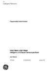
GE Fanuc Automation Programmable Control Products IC697VDR150 / IC697VDR151 Relay Board with BIT User’s Manual GFK-2063 514-000441-000 A December 2001 GFL-002 Warnings, Cautions, and Notes as Used in this Publication Warning Warning notices are used in this publication to emphasize that hazardous voltages, currents, temperatures, or other conditions that could cause personal injury exist in this equipment or may be associated with its use. In situations where inattention could cause either personal injury or damage to equipment, a Warning notice is used. Caution Caution notices are used where equipment might be damaged if care is not taken. Note Notes merely call attention to information that is especially significant to understanding and operating the equipment. This document is based on information available at the time of its publication. While efforts have been made to be accurate, the information contained herein does not purport to cover all details or variations in hardware or software, nor to provide for every possible contingency in connection with installation, operation, or maintenance. Features may be described herein which are not present in all hardware and software systems. GE Fanuc Automation assumes no obligation of notice to holders of this document with respect to changes subsequently made. GE Fanuc Automation makes no representation or warranty, expressed, implied, or statutory with respect to, and assumes no responsibility for the accuracy, completeness, sufficiency, or usefulness of the information contained herein. No warranties of merchantability or fitness for purpose shall apply. The following are trademarks of GE Fanuc Automation North America, Inc. Alarm Master CIMPLICITY CIMPLICITY 90–ADS CIMSTAR Field Control GEnet Genius Helpmate Logicmaster Modelmaster Motion Mate ProLoop PROMACRO PowerMotion PowerTRAC Series 90 Series Five Series One ©Copyright 2001 GE Fanuc Automation North America, Inc. All Rights Reserved Series Six Series Three VersaMax VersaPro VuMaster Workmaster Contents Chapter 1 Introduction, Description, and Specifications ......................................... 1-1 Reference Material and Other GE Fanuc Manuals................................................... 1-1 General Description ................................................................................................. 1-2 Functional Description ............................................................................................. 1-3 Safety Summary ....................................................................................................... 1-4 Chapter 2 Configuration and Installation.................................................................. 2-1 Physical Installation ................................................................................................. 2-2 Jumper Installations ................................................................................................. 2-3 Connector Configuration.......................................................................................... 2-7 Chapter 3 Programming.............................................................................................. 3-1 Introduction.............................................................................................................. 3-2 Register Map ............................................................................................................ 3-3 Built-in-Test ............................................................................................................. 3-8 Chapter 4 Theory of Operation .................................................................................. 4-1 Internal Functional Organization ............................................................................. 4-2 Foundation Logic ..................................................................................................... 4-3 Output Registers and Relays .................................................................................... 4-8 Built-in-Test (BIT) ................................................................................................... 4-9 Chapter 5 GFK-2063 Maintenance................................................................................................ 5-1 iii Chapter Introduction, Description, and Specifications 1 This manual describes the features, installation, and operation of the following relay output modules with built-in test logic: Part Number Channels Connectors Contact Type IC697VDR150 32 channels two 96-pin DIN connectors Non-latching IC697VDR151 64 channels two 96-pin DIN connectors Non-latching Reference Material and Other GE Fanuc Manuals For a detailed explanation of the VMEbus and its characteristics, “The VMEbus Specification” is available from: VITA VMEbus International Trade Association 7825 East Gelding Dr., No. 104 Scottsdale, AZ 85260 (480) 951-8866 FAX: (480) 951-0720 Internet: www.vita.com The following Application Guide is available from GE Fanuc to assist in the selection, specification, and implementation of systems based upon GE Fanuc’s products: Connector and I/O Cable Application Guide (catalog number GFK-2085) GFK-2063 Describes I/O connections that can be used with GE Fanuc’s VMEbus products. Includes connector compatibility information and examples. 1-1 1 General Description The Relay Board is VMEbus-compatible. Some of the board’s other features include: • 1 Form C contacts (SPDT) • 2.0 A / 60 W contact rating • Protection from relays changing during power changes • BIT checks the contacts as well as the driving registers • 8-, 16-, or 32-bit Data Transfers • User selected Short I/O or Standard Data addressing • User selected supervisory, nonprivileged, or either access Two 96-pin DIN compatible connectors are provided on the board and are accessible from the front panel. Each relay uses one row of pins. The A column connects to the NO (normally open) contact, the B column connects to the NC (normally closed) contact, and the C column connects to the Common contact. A 64-conductor cable can be used to switch the Normally Open, 1 Form A (SPST) contacts. 1-2 IC697VDR150 / IC697VDR151 Relay Board with BIT User’s Manual – December 2001 GFK-2063 1 Functional Description The Relay Board is a digital output board. Writing a logic "one" to a register on the board will activate the associated relay. When a relay is activated, its Normally Open (NO) contacts close and its Normally Closed (NC) contacts open. Writing a logic "zero" to a register will deactivate the relay and its contacts will return to their normal positions. The Relay Board consists of VMEbus foundation logic, data output control logic, relays, and BIT logic. The foundation logic conforms to the VMEbus requirements and contains the board select and data steering logic. The data output control logic decodes the desired on-board register the data goes to and stores the data. The relays have their contacts available at the two front panel connectors. The BIT logic tests the Data Output Registers by using a built-in feedback function in the chip. The BIT logic monitors a second set of relay contacts, allowing BIT to test the relays and their driving logic. GFK-2063 Chapter 1 Introduction, Description, and Specifications 1-3 1 Safety Summary Warning The following general safety precautions must be observed during all phases of operation, service, and repair of this product. Failure to comply with these precautions or with specific warnings elsewhere in this manual violates safety standards of design, manufacture, and intended use of this product. GE Fanuc assumes no liability for the customer’s failure to comply with these requirements. Ground the System To minimize shock hazard, the chassis and system cabinet must be connected to an electrical ground. A three-conductor AC power cable should be used. The power cable must either be plugged into an approved three-contact electrical outlet or used with a three-contact to two-contact adapter with the grounding wire (green) firmly connected to an electrical ground (safety ground) at the power outlet. Do Not Operate in an Explosive Atmosphere Do not operate the system in the presence of flammable gases or fumes. Operation of any electrical system in such an environment constitutes a definite safety hazard. Keep Away from Live Circuits Operating personnel must not remove product covers. Component replacement and internal adjustments must be made by qualified maintenance personnel. Do not replace components with power cable connected. Under certain conditions, dangerous voltages may exist even with the power cable removed. To avoid injuries, always disconnect power and discharge circuits before touching them. Do Not Service or Adjust Alone Do not attempt internal service or adjustment unless another person, capable of rendering first aid and resuscitation, is present. Do Not Substitute Parts or Modify System Because of the danger of introducing additional hazards, do not install substitute parts or perform any unauthorized modification to the product. Return the product to GE Fanuc for service and repair to ensure that safety features are maintained. 1-4 IC697VDR150 / IC697VDR151 Relay Board with BIT User’s Manual – December 2001 GFK-2063 Chapter Configuration and Installation 2 This chapter, divided into the following sections, provides configuration and installation instructions for the Relay Board: Physical Installation Jumper Installations Connector Configuration Caution Some of the components assembled on GE Fanuc products can be sensitive to electrostatic discharge and damage can occur on boards that are subjected to a high-energy electrostatic field. When the board is placed on a bench for configuring, etc., it is suggested that conductive material be placed under the board to provide a conductive shunt. Unused boards should be stored in the same protective boxes in which they were shipped. Upon receipt, any precautions found in the shipping container should be observed. All items should be carefully unpacked and thoroughly inspected for damage that might have occurred during shipment. The board(s) should be checked for broken components, damaged printed circuit board(s), heat damage, and other visible contamination. All claims arising from shipping damage should be filed with the carrier and a complete report sent to GE Fanuc together with a request for advice concerning the disposition of the damaged item(s). GFK-2063 2-1 2 Physical Installation Caution Do not install or remove board while power is applied. De-energize the equipment and insert the board into an appropriate slot of the chassis. While ensuring that the board is properly aligned and oriented in the supporting board guides, slide the board smoothly forward against the mating connector until firmly seated. 2-2 IC697VDR150 / IC697VDR151 Relay Board with BIT User’s Manual – December 2001 2 Jumper Installations There are 22 jumper positions in one header located in the middle of the bus side of the board. Figure 2-1 on page 2-4 shows the relative position of this header. Each jumper position is labeled on the board as shown in Figure 2-2 on page 2-5. This figure is an enlarged view of the silkscreen text. To configure the board, first determine what address range the board will occupy. If the board goes in the Standard Data address space, install a jumper in the SHT/ STD I/O position. This is the jumper closest to the edge of the board. The board is shipped from the factory using the Short I/O address space as shown in Figure 2-3 on page 2-5. The next jumper installation is based on which access mode the board will use. Boards that use the Nonprivileged only mode will have a jumper placed in the AM2 position. This is the third jumper from the edge of the board. Figure 2-4 on page 2-5 shows this jumper. Boards that will use either Nonpriviliged or Supervisory modes will have a jumper placed on the "(AM2/ AM2 )" position. This is the second jumper from the edge of the board. The board is shipped from the factory configured to respond to both supervisory and nonprivileged accesses as shown in Figure 25 on page 2-6. For boards that use Supervisory only mode, no jumper would be used in these places. If both jumpers are installed, the board will respond to nonprivileged accesses. The remaining 19 jumper positions correspond to the address line listed beside the jumper. These jumpers create the base address of the board. Place a jumper on the posts in the position where an address line is to be "zero" in the base address of the board. For boards that use Short I/O addresses, jumpers placed on the posts in the positions A16 through A23 have no effect. They are not used. Of course, for boards using Standard Data addresses, these jumpers are used. Figure 2-7 on page 2-6 shows a Short I/O address of A5C0 HEX. GFK-2063 Chapter 2 Configuration and Installation 2-3 2 Figure 2-1: Jumper Locations P3 P1 43 44 H1 P4 1 2 COM PON 2-4 ENT SIDE P2 IC697VDR150 / IC697VDR151 Relay Board with BIT User’s Manual – December 2001 2 Figure 2-2: Jumper Labels 43 Figure 2-3: SHT/STD I/O Jumper Factory Configuration A07 44 A23 A06 A22 A05 A21 AM2 AM2 AM2 ( A20 ) SHT/STD I/O A19 A18 A17 A16 A15 Figure 2-4: Nonprivileged Only Mode Configuration A14 A13 A07 A12 A06 A11 A05 A10 AM2 AM2 AM2 SHT/STD I/O ( A09 A08 ) A07 A06 A05 ( AM2 AM2 AM2 ) SHT/STD I/O GFK-2063 Chapter 2 Configuration and Installation 2-5 2 Figure 2-5: Either Access Mode Configuration Figure 2-7: Typical Board Configuration 43 A07 A23 A06 A22 A05 ( AM2 AM2 AM2 44 A21 A20 ) A19 SHT/STD I/O A18 A17 A16 A15 A14 Figure 2-6: AM2 Configuration Error A13 A12 A07 A11 A06 A10 A05 ( AM2 AM2 AM2 A09 A08 ) A07 SHT/STD I/O A06 A05 ( This will cause a system malfunction. AM2 AM2 AM2 ) SHT/STD I/O The configuration is for a Short I/O Board using either access mode with a base address of $A5C0. 2-6 IC697VDR150 / IC697VDR151 Relay Board with BIT User’s Manual – December 2001 2 Connector Configuration The Relay Board uses two 96-pin DIN connectors on the front panel. These connectors can be used with a discrete wire connector housing and shell from HARTING ELEKTRONIK INC. or a massterminated cable and connector from ERNI components. The specification sheet for this board contains detailed ordering information about these connectors and cables. These cables and connectors will bring out all of the contacts from the board. The contacts are configured as 1 Form C (SPDT); however, the connector layout shown in Figure 2-8 below and Figure 2-9 on page 2-8 permits a 64-conductor cable and full C DIN connector to bring out the contacts as a 1 Form A (SPST N.O.). Figure 2-8: P3’s Connector Layout and Pin Assignments PC Board A B C GFK-2063 Column A Column B Column C Channel A32 – N.O. B32 – N.C. C32 – COMM CHNL 63 A31 – N.O. B31 – N.C. C31 – COMM CHNL 62 A30 – N.O. B30 – N.C. C30 – COMM CHNL 61 A29 – N.O. B29 – N.C. C29 – COMM CHNL 60 A28 – N.O. B28 – N.C. C28 – COMM CHNL 59 A27 – N.O. B27 – N.C. C27 – COMM CHNL 58 A26 – N.O. B26 – N.C. C26 – COMM CHNL 57 A25 – N.O. B25 – N.C. C25 – COMM CHNL 56 A24 – N.O. B24 – N.C. C24 – COMM CHNL 55 A23 – N.O. B23 – N.C. C23 – COMM CHNL 54 A22 – N.O. B22 – N.C. C22 – COMM CHNL 53 A21 – N.O. B21 – N.C. C21 – COMM CHNL 52 A20 – N.O. B20 – N.C. C20 – COMM CHNL 51 A19 – N.O. B19 – N.C. C19 – COMM CHNL 50 A18 – N.O. B18 – N.C. C18 – COMM CHNL 49 A17 – N.O. B17 – N.C. C17 – COMM CHNL 48 A16 – N.O. B16 – N.C. C16 – COMM CHNL 47 A15 – N.O. B15 – N.C. C15 – COMM CHNL 46 A14 – N.O. B14 – N.C. C14 – COMM CHNL 45 A13 – N.O. B13 – N.C. C13 – COMM CHNL 44 A12 – N.O. B12 – N.C. C12 – COMM CHNL 43 A11 – N.O. B11 – N.C. C11 – COMM CHNL 42 A10 – N.O. B10 – N.C. C10 – COMM CHNL 41 A09 – N.O. B09 – N.C. C09 – COMM CHNL 40 A08 – N.O. B08 – N.C. C08 – COMM CHNL 39 A07 – N.O. B07 – N.C. C07 – COMM CHNL 38 A06 – N.O. B06 – N.C. C06 – COMM CHNL 37 A05 – N.O. B05 – N.C. C05 – COMM CHNL 36 A04 – N.O. B04 – N.C. C04 – COMM CHNL 35 A03 – N.O. B03 – N.C. C03 – COMM CHNL 34 A02 – N.O. B02 – N.C. C02 – COMM CHNL 33 A01 – N.O. B01 – N.C. C01 – COMM CHNL 32 Chapter 2 Configuration and Installation 2-7 2 Figure 2-9: P4’s Connector Layout and Pin Assignments Column A PC Board A B C 2-8 Column B Column C Channel A32 – N.O. B32 – N.C. C32 – COMM CHNL 31 A31 – N.O. B31 – N.C. C31 – COMM CHNL 30 A30 – N.O. B30 – N.C. C30 – COMM CHNL 29 A29 – N.O. B29 – N.C. C29 – COMM CHNL 28 A28 – N.O. B28 – N.C. C28 – COMM CHNL 27 A27 – N.O. B27 – N.C. C27 – COMM CHNL 26 A26 – N.O. B26 – N.C. C26 – COMM CHNL 25 A25 – N.O. B25 – N.C. C25 – COMM CHNL 24 A24 – N.O. B24 – N.C. C24 – COMM CHNL 23 A23 – N.O. B23 – N.C. C23 – COMM CHNL 22 A22 – N.O. B22 – N.C. C22 – COMM CHNL 21 A21 – N.O. B21 – N.C. C21 – COMM CHNL 20 A20 – N.O. B20 – N.C. C20 – COMM CHNL 19 A19 – N.O. B19 – N.C. C19 – COMM CHNL 18 A18 – N.O. B18 – N.C. C18 – COMM CHNL 17 A17 – N.O. B17 – N.C. C17 – COMM CHNL 16 A16 – N.O. B16 – N.C. C16 – COMM CHNL 15 A15 – N.O. B15 – N.C. C15 – COMM CHNL 14 A14 – N.O. B14 – N.C. C14 – COMM CHNL 13 A13 – N.O. B13 – N.C. C13 – COMM CHNL 12 A12 – N.O. B12 – N.C. C12 – COMM CHNL 11 A11 – N.O. B11 – N.C. C11 – COMM CHNL 10 A10 – N.O. B10 – N.C. C10 – COMM CHNL 09 A09 – N.O. B09 – N.C. C09 – COMM CHNL 08 A08 – N.O. B08 – N.C. C08 – COMM CHNL 07 A07 – N.O. B07 – N.C. C07 – COMM CHNL 06 A06 – N.O. B06 – N.C. C06 – COMM CHNL 05 A05 – N.O. B05 – N.C. C05 – COMM CHNL 04 A04 – N.O. B04 – N.C. C04 – COMM CHNL 03 A03 – N.O. B03 – N.C. C03 – COMM CHNL 02 A02 – N.O. B02 – N.C. C02 – COMM CHNL 01 A01 – N.O. B01 – N.C. C01 – COMM CHNL 00 IC697VDR150 / IC697VDR151 Relay Board with BIT User’s Manual – December 2001 Chapter Programming 3 This chapter contains programming instructions for the Relay Board, and is divided into the following sections: GFK-2063 Introduction Register Map Built-in-Test 3-1 3 Introduction Writing a "one" to a particular bit position will activate the associated relay on the 64-channel relay output board. Writing a "zero" to the bit will deactivate the relay. The board has an identity register for system software to automatically determine what boards are in the system. A Control and Status Register is provided for user control of the relay drivers, while a front panel LED may be illuminated by software to detect a faulty board in a system. All registers can be accessed on read or write cycles. Some of the registers, including the Board Identification Register (BDID) and the Relay Contact Registers, are only valid during read transfers. The board responds to write accesses to these registers but data is not stored. The 32-channel board (IC697VRD150) uses registers 00 through 31. The unused registers are decoded and the board responds to these transfers, however the data is lost. These registers are noted in the "Register Map" section. This chapter of the manual uses the dollar sign ($) to denote hexadecimal numbers. 3-2 IC697VDR150 / IC697VDR151 Relay Board with BIT User’s Manual – December 2001 3 Register Map The Board’s BDID is located at its base address. A Control and Status Register (CSR) is stacked on the next word boundary. This is followed by the Relay Control or Output Registers beginning at an offset of 10 HEX from the base address of the board. Finally, the Relay Contact Registers are placed at the next word boundary. Table 3-1 below lists these registers with their byte offsets. The offset addresses listed in the register map are relative to the base address the user sets up with the jumpers supplied on header H1. The offsets are shown in hexadecimal. The register names correspond to their control line signal names in the schematic. Table 3-2 on page 3-4 lists the individual bit definitions for these registers and the bit position on the board’s internal data bus. These definitions determine what relay is being controlled by a particular register and data line. Board ID Register This register is located at the base address of the board and contains a fixed value ($1Bxx when read as a word from offset $00). This is for automatic system configuration software. Table 3-1: Register Map Offset Name Description $00 BDID ID register with fixed data of $1B. $01 RESERVED Not Used, Reads as XX $02 CSR Controls the relay drivers and front panel LED. $03 RESERVED Not Used, Reads as XX • • • • • • • $0F • RESERVED • $10 RELAY_CTRL_REG 0* Controls relay channels 63 to 56.* $11 $12 RELAY_CTRL_REG 1* RELAY_CTRL_REG 2* Controls relay channels 55 to 48.* Controls relay channels 47 to 40.* $13 RELAY_CTRL_REG 3* Controls relay channels 39 to 32.* $14 RELAY_CTRL_REG 4 Controls relay channels 31 to 24. $15 RELAY_CTRL_REG 5 Controls relay channels 23 to 16. $16 RELAY_CTRL_REG 6 Controls relay channels 15 to 09. $17 RELAY_CTRL_REG 7 Controls relay channels 07 to 00. $18 RLY_CONTACT_REG 0* Reads the contacts of relay channels 63 to 56.* $19 RLY_CONTACT_REG 1* Reads the contacts of relay channels 55 to 48.* Not Used, Reads as XX $1A RLY_CONTACT_REG 2* Reads the contacts of relay channels 47 to 40.* $1B RLY_CONTACT_REG 3* Reads the contacts of relay channels 39 to 32.* $1C $1D RLY_CONTACT_REG 4 RLY_CONTACT_REG 5 Reads the contacts of relay channels 31 to 24. Reads the contacts of relay channels 23 to 16. $1E RLY_CONTACT_REG 6 Reads the contacts of relay channels 15 to 08. $1F RLY_CONTACT_REG 7 Reads the contacts of relay channels 07 to 00. * These registers are not used in the 32-channel version of this board (VRD150). GFK-2063 Chapter 3 Programming 3-3 3 Table 3-2: Register Bit Definitions Board ID Register (Offset $00) BDID Bit 31 Bit 30 Bit 29 Bit 28 Bit 27 Bit 26 Bit 25 Bit 24 0 0 0 1 1 0 1 1 Bit 09 Bit 08 Board ID Register (Offset $02) CSR Bit 15 Bit 14 Bit 13 Fail LED OFF TEST MODE P4 OFF TEST MODE P3 OFF Bit 12 Bit 11 Bit 10 Not Used (Offset $10) RELAY_CTRL_REG 0* Bit 31 Bit 30 Bit 29 Bit 28 Bit 27 Bit 26 Bit 25 Bit 24 SET RELAY CHNL 63 SET RELAY CHNL 62 SET RELAY CHNL 61 SET RELAY CHNL 60 SET RELAY CHNL 59 SET RELAY CHNL 58 SET RELAY CHNL 57 SET RELAY CHNL 56 (Offset $11) RELAY_CTRL_REG 1* Bit 23 Bit 22 Bit 21 Bit 20 Bit 19 Bit 18 Bit 17 Bit 16 SET RELAY CHNL 55 SET RELAY CHNL 54 SET RELAY CHNL 53 SET RELAY CHNL 52 SET RELAY CHNL 51 SET RELAY CHNL 50 SET RELAY CHNL 49 SET RELAY CHNL 48 (Offset $12) RELAY_CTRL_REG 2* Bit 15 Bit 14 Bit 13 Bit 12 Bit 11 Bit 10 Bit 09 Bit 08 SET RELAY CHNL 47 SET RELAY CHNL 46 SET RELAY CHNL 45 SET RELAY CHNL 44 SET RELAY CHNL 43 SET RELAY CHNL 42 SET RELAY CHNL 41 SET RELAY CHNL 40 (Offset $13) RELAY_CTRL_REG 3* 3-4 Bit 07 Bit 06 Bit 05 Bit 04 Bit 03 Bit 02 Bit 01 Bit 00 SET RELAY CHNL 39 SET RELAY CHNL 38 SET RELAY CHNL 37 SET RELAY CHNL 36 SET RELAY CHNL 35 SET RELAY CHNL 34 SET RELAY CHNL 33 SET RELAY CHNL 32 IC697VDR150 / IC697VDR151 Relay Board with BIT User’s Manual – December 2001 3 (Offset $14) RELAY_CTRL_REG 4* Bit 31 Bit 30 Bit 29 Bit 28 Bit 27 Bit 26 Bit 25 Bit 24 SET RELAY CHNL 31 SET RELAY CHNL 30 SET RELAY CHNL 29 SET RELAY CHNL 28 SET RELAY CHNL 27 SET RELAY CHNL 26 SET RELAY CHNL 25 SET RELAY CHNL 24 (Offset $15) RELAY_CTRL_REG 5* Bit 23 Bit 22 Bit 21 Bit 20 Bit 19 Bit 18 Bit 17 Bit 16 SET RELAY CHNL 23 SET RELAY CHNL 22 SET RELAY CHNL 21 SET RELAY CHNL 20 SET RELAY CHNL 19 SET RELAY CHNL 18 SET RELAY CHNL 17 SET RELAY CHNL 16 (Offset $16) RELAY_CTRL_REG 6* Bit 15 Bit 14 Bit 13 Bit 12 Bit 11 Bit 10 Bit 09 Bit 08 SET RELAY CHNL 15 SET RELAY CHNL 14 SET RELAY CHNL 13 SET RELAY CHNL 12 SET RELAY CHNL 11 SET RELAY CHNL 10 SET RELAY CHNL 09 SET RELAY CHNL 08 (Offset $17) RELAY_CTRL_REG 7* Bit 07 Bit 06 Bit 05 Bit 04 Bit 03 Bit 02 Bit 01 Bit 00 SET RELAY CHNL 07 SET RELAY CHNL 06 SET RELAY CHNL 05 SET RELAY CHNL 04 SET RELAY CHNL 03 SET RELAY CHNL 02 SET RELAY CHNL 01 SET RELAY CHNL 00 (Offset $18) RLY_CONTACT_REG 0* Bit 31 Bit 30 Bit 29 Bit 28 Bit 27 Bit 26 Bit 25 Bit 24 RELAY CNTCT 63 RELAY CNTCT 62 RELAY CNTCT 61 RELAY CNTCT 60 RELAY CNTCT 59 RELAY CNTCT 58 RELAY CNTCT 57 RELAY CNTCT 56 (Offset $19) RLY_CONTACT_REG 1* GFK-2063 Bit 23 Bit 22 Bit 21 Bit 20 Bit 19 Bit 18 Bit 17 Bit 16 RELAY CNTCT 55 RELAY CNTCT 54 RELAY CNTCT 53 RELAY CNTCT 52 RELAY CNTCT 51 RELAY CNTCT 50 RELAY CNTCT 49 RELAY CNTCT 48 Chapter 3 Programming 3-5 3 (Offset $1A) RLY_CONTACT_REG 2* Bit 15 Bit 14 Bit 13 Bit 12 Bit 11 Bit 10 Bit 09 Bit 08 RELAY CNTCT 47 RELAY CNTCT 46 RELAY CNTCT 45 RELAY CNTCT 44 RELAY CNTCT 43 RELAY CNTCT 42 RELAY CNTCT 41 RELAY CNTCT 40 (Offset $1B) RLY_CONTACT_REG 3* Bit 07 Bit 06 Bit 05 Bit 04 Bit 03 Bit 02 Bit 01 Bit 00 RELAY CNTCT 39 RELAY CNTCT 38 RELAY CNTCT 37 RELAY CNTCT 36 RELAY CNTCT 35 RELAY CNTCT 34 RELAY CNTCT 33 RELAY CNTCT 32 (Offset $1C) RLY_CONTACT_REG 4* Bit 31 Bit 30 Bit 29 Bit 28 Bit 27 Bit 26 Bit 25 Bit 24 RELAY CNTCT 31 RELAY CNTCT 30 RELAY CNTCT 29 RELAY CNTCT 28 RELAY CNTCT 27 RELAY CNTCT 26 RELAY CNTCT 25 RELAY CNTCT 24 (Offset $1D) RLY_CONTACT_REG 5* Bit 23 Bit 22 Bit 21 Bit 20 Bit 19 Bit 18 Bit 17 Bit 16 RELAY CNTCT 23 RELAY CNTCT 22 RELAY CNTCT 21 RELAY CNTCT 20 RELAY CNTCT 19 RELAY CNTCT 18 RELAY CNTCT 17 RELAY CNTCT 16 (Offset $1E) RLY_CONTACT_REG 6* Bit 15 Bit 14 Bit 13 Bit 12 Bit 11 Bit 10 Bit 09 Bit 08 RELAY CNTCT 15 RELAY CNTCT 14 RELAY CNTCT 13 RELAY CNTCT 12 RELAY CNTCT 11 RELAY CNTCT 10 RELAY CNTCT 09 RELAY CNTCT 08 (Offset $1F) RLY_CONTACT_REG 7* Bit 07 Bit 06 Bit 05 Bit 04 Bit 03 Bit 02 Bit 01 Bit 00 RELAY CNTCT 07 RELAY CNTCT 06 RELAY CNTCT 05 RELAY CNTCT 04 RELAY CNTCT 03 RELAY CNTCT 02 RELAY CNTCT 01 RELAY CNTCT 00 * These registers are not used with the 32-channel board (VRD150) and are not driven by the board. 3-6 IC697VDR150 / IC697VDR151 Relay Board with BIT User’s Manual – December 2001 3 Control and Status Register (CSR) The CSR is used to control the relay drivers and a front panel LED. This register has three active bits (15 to 13). The rest of the bits are not used, but they are read back. Bit 15 controls the front panel Fail LED. When a zero is written to this bit, the LED will turn ON. This bit is cleared when power is applied, or after a system reset. However, it is under program control and can be used to locate faulty boards in a system. Bits 14 and 13 control the relay drivers. Registers that store data control the relays. The outputs of these registers go to the drivers, which then activate the relays. These drivers can be disabled by the CSR. Bit 14 controls the relays going to connector P4 (Channels 1 through 32). Bit 13 controls the relays of P3 (Channels 33 through 64). Writing a zero to either of these bits will disable the drivers associated with the listed output channels. For nonlatching relays, they will go to their normal contact positions (normally open contacts will open and normally closed contacts will close). Like Bit 15, these bits will be cleared when power is applied (or after a system reset) in order to prevent random data from disturbing the field circuitry controlled by these relays. Relay Control Registers These registers control the relay drivers and hence the relays. Each bit controls one relay. The relay or output channel for each bit is listed in Table 3-2 on page 3-4. Writing a logic "one" to this bit will activate the set relay coil. This will force the normally closed contact to open and the normally open contact to close. The relay will close its normally closed contact and open the normally open contact whenever a logic "zero" is written to its control bit. Relay Contact Registers These registers contain the state of a second set of contacts in the relays. This contact reflects the condition of the contacts, which may take as much as 5.5 msec to finally switch after a change command is sent to its Control Register. The logic level read from this register bit will match the level in the Control Register’s bit after the contact has had enough time to settle into its new position. If a logic "one" is written to Control Register 5, Bit 19, channel 19 will switch to its active state. Normally open contacts will close, etc. 7 msec later reading Contact Register 5, Bit 19 and will show a logic "one", just like its counterpart in the Control Register. GFK-2063 Chapter 3 Programming 3-7 3 Built-in-Test Built-in-Test is done by reading back the data written to a specific register and comparing it to the data written. All board registers are available to the user at any time. There are two types of testing done with this board, off-line (Testmode) or on-line (real-time). In Testmode testing, the relay drivers are disabled. This will prevent test data from disturbing the external circuitry. However, it also fails to test the relays themselves. Testmode is useful during initial testing to determine if the board can respond to commands without risking damage to any sensitive controllers or equipment. Since Testmode can be performed at any time, two bits are used in order to keep half of the board active, while the other half is in Testmode. The Relay Contact Registers are used to permit checking of the relays. These registers show the state of a second set of contacts in each relay. Their logic state will reflect the logic state of the Control Registers after the contacts have stopped bouncing. If the Control Register has a logic "one" in a certain bit, then the Contact Register will also have a logic "one" in the associated bit position. These registers permit testing of all of the components on the board up to the output connectors. 3-8 IC697VDR150 / IC697VDR151 Relay Board with BIT User’s Manual – December 2001 Chapter Theory of Operation 4 This chapter describes the internal organization of the Relay Board, reviews the general principles of operation, and is divided into the following sections: GFK-2063 Internal Functional Organization Foundation Logic Output Registers and Relays Built-in-Test (BIT) 4-1 4 Internal Functional Organization To activate a relay on the board, write a "one" to the address and bit position for that output channel. To check on the "health" of the board, read a register and compare this data to the written data. A Board Identification Register and a Control and Status Register are available for controlling the board. A block diagram of the board is shown in Figure 4-1 below. The Relay Board has three basic sections: the foundation logic, the output control logic, and the relays. The foundation logic contains the board address decoder and the data steering logic. The output control logic decodes the on-board registers and places the data in the appropriate register or activates the proper register for read accesses. The relays simply place their contacts on the output connectors that will go to the external circuits being controlled. Figure 4-1: Relay Board Block Diagram FOUNDATION LOGIC P3/P4 8 A24 V ADDRESS BOARD DECODER SELECT A16 M E CTRL LINES b OUTPUT 128 REGISTER 64 VMEbus DECODER 2 FORM C STATE WITH RELAYS BIT u s DATA 16 16 4-2 RELAY STEERING IDB CONTACT LOGIC 32 BIT 64 REGISTERS IC697VDR150 / IC697VDR151 Relay Board with BIT User’s Manual – December 2001 192 4 Foundation Logic The foundation logic provides the proper loading to the VMEbus via components used in building the board. The foundation logic also decides if this board is to respond to a VMEbus data cycle, steers the data to or from the proper on-board registers, and issues DTACK* to the host CPU. Address Decoding The address decoder (shown in Figure 4-2 on page 4-5) determines when the board will respond to a VMEbus data transfer cycle. The decoder has three address comparators and their associated board address jumpers in header H1. There are two additional jumpers (also part of H1) involved in the decode function. One of them is the Short/Standard Addressing jumper. The other is the Supervisory/Nonprivileged jumper. The Short/Standard Addressing jumper determines if the upper eight address lines (A23-A16) will be used in the board’s base address. When this jumper is not installed, the upper eight address lines are ignored. This puts the board in the A16 or Short I/O address range. If the jumper is installed, the upper eight lines are used. This jumper and the AM2 (or Supervisory/Nonprivileged) jumper determine what address modifier the board will respond to. The Supervisory/Nonprivileged jumper has two positions. The positions are labeled AM2 and AM2/ AM2 . Install a jumper in the AM2 location when the board is to respond to a nonprivileged access only. Install a jumper at the AM2/ AM2 position when the board is to respond to either nonprivileged or supervisory accesses. If a response is desired for supervisory access only, do not install a jumper in either position. Do not install both jumpers. If both jumpers are installed, the AM2 line to the VMEbus backplane will be grounded and the system will not work properly. The rest of the positions in the header H1 are used to establish the base address of the board. Any installed jumper will set the corresponding address line to a logic low in the comparators. This address line is listed next to the jumper position. If the board is set up for Short I/O accesses, any jumpers installed in the upper eight positions (A(16) through A(23)) are ignored. They do not have to be removed. GFK-2063 Chapter 4 Theory of Operation 4-3 4 Data Steering and Register Decoding Once the decoder decides to respond, BD_SEL_H is asserted (driven high). This signal clocks the state of the VMEbus control lines and the four lowest address lines into a register. The outputs of this register are used to decode the internal board functions. The outputs of this decoder (shown in Figure 4-3 on page 4-6) engage data transceivers, who steer the data to the proper internal register. The data transceivers then clock this data into a register or place data on the Internal Data Bus (IDB), depending upon the type of data cycle. Storing the VMEbus state permits the host to prepare the next transaction while the Relay Board is still processing the present data cycle. These signals are decoded and the proper register(s) are activated. If a write cycle is in progress, the clock signal will store the data from the VMEbus into the selected register(s). The clock signal is delayed long enough for the data to move through the steering logic and be present and stable before the register(s) are clocked. During a read cycle, the proper register(s) have their data placed on the IDB and it is held there until the end of the transfer cycle (when both Data Strobe lines go high). All of the board’s registers can be read from, or written to, at any time. However, data written to read only registers (BDID and Relay Contact Registers) will be lost. The CSR contains control lines that determine what relay drivers are active. The BDID and CSR will be discussed in more detail in the next section. Once the board determines it is to respond to a bus cycle, DTACK* is asserted (driven low) 150 nsec (nanoseconds) later. This tells the host when the board is done with the data. The host withdraws its Data Strobes by driving them high. The Relay Board sees this and rearms its board select logic, then waits for the next data cycle. 4-4 IC697VDR150 / IC697VDR151 Relay Board with BIT User’s Manual – December 2001 4 Figure 4-2: Board Select Logic A4 to A1, WR L, LWD L AM0 to AM5 BOARD SELECT LOGIC BD SEL H SHT/STD P=Q VMEbus STATE REGISTER 8-bit AM2 A07 to A05 V M E b u s COMPARATOR P Q AM2 AM2+AM2 A07 to A05 H1 P=Q 8-bit COMPARATOR A15 to A08 P Q A15 to A08 P=Q 8-bit COMPARATOR A24 to A16 GFK-2063 P Q Chapter 4 Theory of Operation A24 to A16 4-5 4 Figure 4-3: Board Register Decoder and Data Steering Logic RD WD 0 to 3L LATCHED A1 to A4 LATCHED LWDL and ON-BOARD REGISTER DECODER RD RLY WD 0 to 3L CLK BYTE 0 to 7 RD BDID and CSR L DLYD BD SEL H, TOGGLE DS0L and DS1L CLK CSR H HI WD BUS EN L SEL HI WD ONLY L LO WD BUS EN L 16 IDB00 to 15 16 IDB16 to 31 D00 to D15 V M E b u s 8-bit XCVR 8-bit XCVR 8-bit XCVR D16 to D31 4-6 IC697VDR150 / IC697VDR151 Relay Board with BIT User’s Manual – December 2001 4 Board ID and Control and Status Registers The BDID is a read only register located at the base address of the board. It has a fixed value of 1BXX HEX. The XX part of this word is not driven by the board and the user should ignore what is read here. The BDID is used by system software to identify the boards in a system for automatic system configuration. If data is written to this address, the board will respond with DTACK*, but the data will not be stored. The CSR is located at the next word location (see Figure 4-4 below shows for BDID and CSR circuitry). The upper three bits (see Chapter 3 for more details) are used by the board and the rest are ignored. The most significant bit (Bit 15) controls the Front Panel Fail LED. When this bit is low, the LED is ON (when it is high, the LED is OFF). The next two bits control the relay drivers. Each bit controls one half of the board’s relays and are broken up by the output connectors. Bit 14 controls the relays going to P4 (Channels 1 through 32). Bit 13 controls the relays going to P3 (Channels 33 through 64). When these bits are high, the drivers are engaged and data written to the Output Registers will control the relays. Write a "one" where a relay is to be activated (i.e. the Normally Open contact is closed, and the Normally Closed contact is open). When a relay is deactivated, the opposite condition exists. If the control bits in the CSR are low, the drivers are tri-stated and the relays are not affected by the data stored in the Output Registers. Figure 4-4: Board ID and CS Registers +5 V CSR Fail LED IDB15 to 08 BIT 13 BIT 14 BIT 15 TEST MODE P3 L TEST MODE P4 L Fail LED L +5 V BDID IDB31 to 24 $1B GFK-2063 Chapter 4 Theory of Operation 4 4 4-7 4 Output Registers and Relays A typical Output Register, relay driver-to-relay circuit is shown in Figure 4-5 on page 4-9. These relays use two coils. One coil is the set coil, which activates the relay. The other is the reset coil. The reset coil will deactivate the relay when it is energized, making it unwise to have both coils active at the same time. To prevent this, the Output Register’s pin goes to a buffer and an inverter driver, leaving only one of the coils energized. The two drivers’ outputs are controlled by the Test Mode bit in the CSR. These drivers cannot be disengaged arbitrarily. They must be active long enough for the relays to change state and latch (7 msec maximum). If the drivers are tri-stated before the relay has had enough time to latch, the relay might switch back to its previous state. To aid the host in determining the state of the relay, a second contact is brought out to the bus via the Relay Contact Register. This contact reflects the state of the relay and is useful in test mode. While in test mode, the Output Registers can be changed without affecting the relays. 4-8 IC697VDR150 / IC697VDR151 Relay Board with BIT User’s Manual – December 2001 4 Built-in-Test (BIT) Built-in-Test is done by reading the appropriate register (Output Registers normally written to by host). To check the Output Registers, perform a read of the same address, then compare the data read to the data written to determine the "health" of these registers. This kind of testing will check most of the circuitry on the board; however, the relays and their drivers are not tested this way. To test relays and their drivers, use the "Relay Contact Register.” These registers return the state of the relay contacts based upon the state the Output Control Register used on the relays. If a "one" is read from the Contact Register, the relay is set or activated, and the data in the Control Register for this relay should also be a "one." The opposite conditions should be found for relays that are reset or deactivated. This discussion assumes that ample time is given to the relays for switching states. RESET COIL DRIVER GFK-2063 Chapter 4 Theory of Operation CLK BYTE x H IDBx RD RLY WD x L IDBx OUTPUT REGISTER TEST MODE P X H SET COIL DRIVER BIT CONTACT D1 +5 V +5 V D2 S 16 R 15 RELAY Kx to ROW A of P3 or P4 to ROW B to ROW C Figure 4-5: Relay and Control Logic 4-9 Chapter Maintenance 5 This chapter provides information relative to the care and maintenance of the Relay Board product. If the product malfunctions, verify the following: • Software • System configuration • Electrical connections • Jumper or configuration settings • Boards are fully inserted into their proper connector location • Connector pins are clean and free from contamination • No components of adjacent boards are disturbed when inserting or removing the board from the chassis • Quality of cables and I/O connections User level repairs are not recommended. Contact your authorized GE Fanuc distributor for a Return Material Authorization (RMA) Number. This RMA Number must be obtained prior to any return. GFK-2063 5-1