1
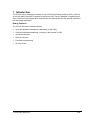
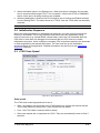
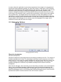
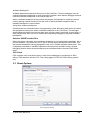
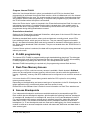
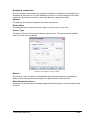
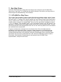
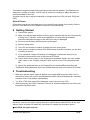
_ V9.12. 225 Technical Notes National CR16C Family On-Chip Emulation This document is intended to be used together with the CPU reference manual provided by the silicon vendor. This document assumes knowledge of the CPU functionality and the terminology and concepts defined and explained in the CPU reference manual. Basic knowledge of winIDEA is also necessary. This document deals with specifics and advanced details and it is not meant as a basic or introductory text. Contents Contents 1 1 Introduction 2 2 Emulation options 2.1 Hardware Options 2.2 Initialization Sequence 2.3 JTAG Scan Speed 3 3 4 4 3 CPU Setup 3.1 General Options 3.2 Debugging Options 3.3 Reset Options 3.4 Advanced Options 5 5 6 7 8 4 FLASH programming 9 5 Real-Time Memory Access 9 6 Access Breakpoints 9 7 On-Chip Trace 7.1 SC14480 On–Chip Trace 7.1.1 Trace Trigger/ Qualifier Configuration 12 12 13 8 Getting Started 14 9 Troubleshooting 14 iSYSTEM, May 2015 1/14 1 Introduction The CR16C family debugging is based on the JTAG Serial Debug Interface (SDI+), which is an on-chip debug interface, compliant to the Nexus 5001 Forum Standard. It implements all basic functions to allow application development and testing with the chip already installed in the final target application. Debug Features The CR16C Emulation System features: Up to six hardware breakpoints (depending on the CPU) Unlimited software breakpoints, including in the internal FLASH Access breakpoints Real-time access Fast flash programming On-Chip Trace iSYSTEM, May 2015 2/14 2 Emulation options 2.1 Hardware Options CR16 Emulation options, Hardware pane Debug I/O levels The development system can be configured in a way that the debug JTAG signals are driven at 3.3V, 5V or target voltage level (Vref). When 'Vref' Debug I/O level is selected, a voltage applied to the belonging reference voltage pin on the target debug connector is used as a reference voltage for voltage follower, which powers buffers, driving the debug JTAG signals. The user must ensure that the target power supply is connected to the Vref pin on the target JTAG connector and that it is switched on before the debug session is started. If these two conditions are not meet, it is highly probably that the initial debug connection will fail already. However in some cases it may succeed but then the system will behave abnormal. This field is grayed in case of CR16C JOWI Debug system, where the debug I/O level is fixed by the iCARD. Hot Attach The JTAG module supports the Hot Attach function. This is a function, which enables the emulator to be connected to a working target device and have all debug functions available. The procedure for Hot Attach: 1. The target application should be running. 2. Hot Attach should be selected in the software. 3. A download should be performed, but without the JTAG cable connected. The emulator will be initialized and the ATTACH status will be shown. 4. Connect the JTAG cable. iSYSTEM, May 2015 3/14 5. Select the Attach option in the Debug menu. When this option is selected, the emulator tries to communicate through JTAG. If it is successful, it shows the STOP or RUNNING status. At this point, all debug functions are available. 6. When the debugging is finished, the CPU should be set to running and Detach selected from the Debug menu. The status shown is ATTACH. Now the JTAG cable can be safely removed. Note: Hot Attach function cannot be used for any flash programming or code download! 2.2 Initialization Sequence Before the flash programming or download can take place, the user must ensure that the memory is accessible. This is very important since there are many applications using memory resources (e.g. external RAM, external flash), which are not accessible after the CPU reset. In that case, the debugger must execute after the CPU reset a so called initialization sequence, which configures necessary CPU chip selects and then the download or flash programming can actually take place. The user must set up the initialization sequence based on his application. Detailed information may be found in the Initialization Sequence help topic. 2.3 JTAG Scan Speed JTAG Scan Speed definition Scan speed The JTAG chain scanning speed can be set to: Slow - long delays are introduced in the JTAG scanning to support the slowest devices. JTAG clock frequency varying from 1 kHz to 2000 kHz can be set. Fast – the JTAG chain is scanned with no delays. Other scan speeds are no supported on CR16. They are automatically forced to Slow if selected. iSYSTEM, May 2015 4/14 In general, Fast mode should be tried for best performance. However, if it fails, try Slow mode at different scan frequencies until you find a working setting. Use – Scan Speed during Initialization On some systems, slower scan speed must be used during initialization, during which the CPU clock is raised (PLL engaged) and then higher scan speeds can be used in operation. In such case, this option and the appropriate scan speed must be selected. 3 CPU Setup 3.1 General Options General options dialog Stop CPU Activities When Stopped When the option is checked, all internal peripherals like timers and counters are stopped when the application is stopped. Otherwise, timers and counters remain running while the program is stopped. Usually, when the option is checked, the emulation system behaves more consistently while stepping through the program. While being aware of the consequences, it is up to the user whether the option is checked or not. For instance, it’s is recommend that a timer, which generates interrupts, is stopped when the application is stopped. Otherwise, the CPU would first service all pending interrupts (generated by the timer while the application was stopped) after the application is resumed. Such behaviour is far away from the actual behaviour of the target application. Cache Downloaded Code only (do not load to target) When this option is checked, the download files will not propagate to the target using standard debug download but the Target download files will. iSYSTEM, May 2015 5/14 In cases, where the application is previously programmed in the target or it's programmed through the flash programming dialog, the user may uncheck 'Load code' in the 'Properties' dialog when specifying the debug download file(s). By doing so, the debugger loads only the necessary debug information for high level debugging while it doesn't load any code. However, debug functionalities like ETM and Nexus trace will not work then since an exact code image of the executed code is required as a prerequisite for the correct trace program flow reconstruction. This applies also for the call stack on some CPU platforms. In such applications, 'Load code' option should remain checked and 'Cache downloaded code only (do not load to target)' option checked instead. This will yield in debug information and code image loaded to the debugger but no memory writes will propagate to the target, which otherwise normally load the code to the target. 3.2 Debugging Options Debugging options dialog Execution breakpoints Hardware Breakpoints Hardware breakpoints are breakpoints that are already provided by the CPU. The number of hardware breakpoints is limited. The advantage is that they function anywhere in the CPU space, which is not the case for software breakpoints, which normally cannot be used in the FLASH memory, non-writeable memory (ROM) or self-modifying code. If the option 'Use hardware breakpoints' is selected, only hardware breakpoints are used for execution breakpoints. Note that the debugger, when executing source step debug command, uses one breakpoint. Hence, when all available hardware breakpoints are used as execution breakpoints, the debugger may fail to execute debug step. The debugger offers 'Reserve one breakpoint for high-level debugging' option in the Debug/Debug Options/Debugging' tab to circumvent this. By default this option is checked and the user can uncheck it anytime. iSYSTEM, May 2015 6/14 Software Breakpoints Available hardware breakpoints often prove to be insufficient. Then the debugger can use unlimited software breakpoints to work around this limitation. Note that the debugger features unlimited software breakpoints in the internal flash too. When a software breakpoint is being used, the program first attempts to modify the source code by placing a break instruction into the code. If setting software breakpoint fails, a hardware breakpoint is used instead. Using flash software breakpoints A flash device has a limited number of programming cycles. Belonging flash sector is erased and programmed every time when a software breakpoint is set or removed. The debugger sets breakpoints hidden from the user also when a source step is executed. In worst case, a flash may become worn out due to intense and long lasting debugging using flash software breakpoints. Set/clear SW BPs before Run When the option is checked, then a software breakpoint is not set/cleared immediately, but is just remembered. Only when the CPU is set to running are the breakpoints committed. This way several breakpoints can be changed but only one re-FLASH operation takes place. This is especially noticeable in testIDEA operation with many stubs and also during a regular debugging session when several breakpoints are set/cleared within the same flash erase block. CPU Clock CPU oscillator clock must be set here in order for the debugger to synchronize its SDI+ debug JTAG interface with the CPU. This setting applies for CR16C JOWI Debug system only. 3.3 Reset Options Reset options dialog iSYSTEM, May 2015 7/14 Stop after target RESET CPU can be optionally stopped after the CPU reset is detected and handled. If the option is unchecked, the application is resumed upon reset release. Reset Method The debugger can reset the CPU through the CPU reset line or through the debug JTAG interface. This setting is not available for CR16C JOWI Debug system. 3.4 Advanced Options Advanced BDM Emulation Options (CR16C and CR16C JOWI) Override startup register values This option overrides the default program counter reset value with the value set. Breakpoints This setting is available only for CPUs with on-chip trace. On-chip debug resources on CPUs featuring on-chip Nexus Trace allow configuration of either 6 execution and 2 access breakpoints or 6 execution breakpoints and 2 trace trigger events. SC14480 CPU doesn’t have a Nexus trace and offers 6 execution and 2 access breakpoints. UBR CR16C CPUs with Nexus trace have a dedicated Nexus register UBR which is used for OTM (Ownership Trace Messaging) trace. An address written in this field is written in the Nexus UBR register through the debug interface. After UBR is programmed, any write from the application to the programmed address yields the belonging OTM message in the trace window. For example, if 0xFFFD00 is written to the UBR, any write to the address 0xFFFD00 in the application, yields OTM record in the trace window. iSYSTEM, May 2015 8/14 Program Internal FLASH When the ‘Use Internal Monitor’ option (not available for all CPUs) is checked, flash programming is performed through fast flash monitor, which is loaded and run in the internal CPU RAM hidden from the user. It’s recommended to have this option checked unless there are problems with the flash programming. A complete flash programming is performed over the JTAG interface when the option is unchecked. When the ‘Entire device’ option is checked in the ‘Erase before download’ field, the user can opt between two options. A complete flash module is erased when ‘Use module erase’ is selected and when ‘Use page erase’ is selected only blocks where the code is going to be programmed during debug download are erased. Erase before download Options in the ‘Erase before download’ field define, which parts of the internal CPU flash are erased before the debug download. Besides a standard flash module, where code and data are normally stored, some CPUs have additional blocks, which are part of flash too. They are named Program Information Block 1 and Data Information Block and can be erased on demand if the belonging option in the ‘Erase before download’ field is checked. They are not erased when the ‘Entire device’ is checked only. If none of these options is selected, the data will be programmed during the debug download without prior erase. 4 FLASH programming The internal CPU FLASH is programmed through standard debug download. The debugger recognizes which code from the download file fits in the internal CPU FLASH. All necessary FLASH programming settings are done in the ‘CPU Setup/Advanced’ dialog. Standard FLASH setup dialog is required only for programming external flash devices. 5 Real-Time Memory Access With this type of CPUs, real-time memory access is available. Watch window’s Rt.Watch panes can be configured to inspect memory with minimum intrusion while the application is running.. Optionally, memory and SFR windows can be configured to use real-time access as well. It is known that the CPU internal debug module stalls few CPU cycles for every debug memory access request. Depending on the application and amount and type of expressions in the Rt. Watch pane, the target application may run differently when real-time access is used. Please refer to the Software User's Guide for more information on Real-Time watches use. 6 Access Breakpoints Four independent breakpoint modules are available and can be accessed through SDI+. Each module has two breakpoint registers, which enable the following functions: breakpoint A, breakpoint B, breakpoint A or breakpoint B, area (from A to B) and breakpoint A then B. For each breakpoint the access method can be selected (execution, data read, data write, data read or write). The software automatically uses 3 breakpoint modules as execution breakpoints (i.e. 5 user breakpoints and one reserved for debugging), the fourth breakpoint module is used as an access breakpoint module with data read, data write and data read or write access types. iSYSTEM, May 2015 9/14 Breakpoint combination Several breakpoint combinations are possible: breakpoint A, breakpoint B, breakpoint A or breakpoint B, area (from A to B) and breakpoint A then B. For each breakpoint the access method can be selected (execution, data read, data write, data read or write). Address The address of the access breakpoint should be entered here. Entire Object If a breakpoint area is defined, the entire object can be set to be in the area. Access Type The Access Type for the Access breakpoint is defined here. The access can be disabled, read only, write only or read/write. Hardware Breakpoints menu, CR16C Wizard… Use Wizard in case of problems understanding and configuring the access breakpoints dialog. It helps setting a simple a breakpoint on data access or code execution. When Breakpoints Occur A beep can be issued and/or a message displayed indicating that an access breakpoint has occurred. iSYSTEM, May 2015 10/14 iSYSTEM, May 2015 11/14 7 On-Chip Trace All CR16 CPUs featuring on-chip trace have Nexus trace except for the SC14480 CPU, which has no trace port. SC14480 has trace buffer already on the silicon (on-chip), which is read through the standard debug JTAG interface. 7.1 SC14480 On–Chip Trace The on-chip Trace controller is able to trace discontinuous program counter values (jumps, calls), data read and write operations and Events, like change of Bus Grant, entry or exit of the trace region, or change of an external signals. All event traces contain timing information using a 32-bit counter, which is clocked with the CPU clock. All trace information is written in a cyclic buffer in internal, non shared RAM. The size of the trace buffer is scalable in sizes 0, 1, 2, 4 or 8kByte. The remaining part of the non-shared memory can be used by the application. Selected trace buffer always resides at the end of the non-shared RAM. The user should pay attention that the application does not use nor write any data into the non-shared ram reserved for the trace buffer. Program and data trace messages are not ordered in time. Since the data trace has precedence over the program trace, a number of data messages is recorded before the actual instruction (block of instructions between two branches, or sync) is recorded that caused the data accesses. No reordering is done by the debugger since it would be highly speculative and cannot be guaranteed to be valid, unless the messages would contain a time-stamp. Unfortunately, time stamps are not realized in the SC14480 Trace implementation, except for the Events. iSYSTEM, May 2015 12/14 SC14480 Trace Trigger/Qualifier dialog 7.1.1 Trace Trigger/ Qualifier Configuration Mode In Single shot mode, the trace stops recording when the buffer becomes full. When in Continuous mode, it records until the trace or the CPU is stopped. Buffer Size Trace buffer resides in the non-shared RAM and is shared with the application. The user should select buffer size considering the trace and application requirements. Qualifier For the instruction trace use, check the Enable Instruction Trace option and check the Enable Data Trace option for the data trace use. Additionally, with the trace start and length registers, the user can define two independent address areas (Range 0 and 1), where instruction and data trace will be active. When the address of an instruction fetch, a data read or write cycle is outside these area’s, no trace record will be written. When neither Range0 nor Range1 is selected, all instruction fetches and data accesses are recorded. iSYSTEM, May 2015 13/14 Two address ranges are defined by specifying a start and end address. The address must always be a multiply of 1kByte. If other value is entered, a rounding to 1kByte boundary is performed hidden to the user. A qualfier can be also a logical combination of ranges and/or two CPU port pins, P2[2] and P2[5]. Record Events Event trace records are generated when one or more Events change from polarity. Refer to the CPU User Manual for more details on specific Events description. 8 Getting Started 1) Connect the system 2) Make sure that the target debug connector pinout matches with the one requested by a debug tool. If it doesn't, make some adaptation to comply with the standard connector otherwise the target or the debug tool may be damaged. 3) Power up the emulator and then power up the target. 4) Execute debug reset 5) The CPU should stop on location to which the reset vector points 6) Open memory window at internal CPU RAM location and check whether you are able to modify its content. 7) If you passed all 6 steps successfully, the debugger is operational and you may proceed to download the code in the internal CPU flash. 8) Check ‘Entire device’ option in the ‘Erase before download' section and ‘Use module erase’ option in the ‘Program internal FLASH’ section in the 'CPU Setup/Advanced' tab. 9) Specify the download file(s) in the 'Debug/Files for download/Download files' tab. 10) Execute Debug download, which should download the code in the internal CPU flash. 9 Troubleshooting Make sure that the power supply is applied to the target BDM connector when ‘Vref’ is selected for Debug I/O levels in the Hardware/Emulator Options/Hardware tab, otherwise emulation fails or may behave unpredictably. Try ‘Slow’ JTAG Scan speed if the debugger cannot connect to the CPU. When performing any kind of checksum, remove all software breakpoints since they may impact the checksum result. Disclaimer: iSYSTEM assumes no responsibility for any errors which may appear in this document, reserves the right to change devices or specifications detailed herein at any time without notice, and does not make any commitment to update the information herein. iSYSTEM. All rights reserved. iSYSTEM, May 2015 14/14