1
Starter Kit LJ12EVB
User’s Manual
Rev 1.0
Brno
November 2002
Content
Introduction---------------------------------------------------------------------------------------------- 5
Who is Beta Control------------------------------------------------------------------------------------ 5
Features of LJ12EVB ---------------------------------------------------------------------------------- 6
Software for LJ12EVB--------------------------------------------------------------------------------- 7
Quick start instructions -------------------------------------------------------------------------------- 7
Configuring the LJ12EVB----------------------------------------------------------------------------- 8
Pinouts --------------------------------------------------------------------------------------------------- 9
NTC/22K Parameters and Nominal Values --------------------------------------------------------- 9
LCD pinout and segments draft---------------------------------------------------------------------- 10
Schematic description --------------------------------------------------------------------------------- 11
LJ12EVB schematic diagram ------------------------------------------------------------------------ 13
LJ12EVB Board Layout ------------------------------------------------------------------------------ 14
Troubleshooting---------------------------------------------------------------------------------------- 15
Starter Kit LJ12EVB
5
Introduction
The Motorola 68HC08 is a very strong and useful product family. The excellent FLASH memory,
various peripheral subsystems, large variety of packages, programming and debugging on-chip
support brings designer’s dreams reality.
The Beta Control’s Low Cost Starter Kit represents very good entry gate to design in. Various
Target Boards could be used as a stand alone board or together with the universal debugger
module. Some instant on board demo peripheral components and associated tutorial programs
enable users to start immediately.
This is ideal tool for any distributors seminars, for the teachers at schools, users clubs and also
for anybody who is interested in application with modern microcontrollers.
Jiri Gutman
Motorola consultant
Who is Beta Control
Beta Control Ltd. is an innovation based company. Its basic strategy consists in utilizing its own
know how of modern technologies in the field of electronic control and information systems.
More then sixty percent of employees are focused on design and development. As the most
products of Beta Controls are based on Motorola technology and products, the Beta Control
became a cooperation partner in promoting Motorola 68HC08 family.
Contact:
Beta Conrol Ltd.
Cerneho 58/60
CZ-635 00 Brno
Czech Republik
Phone: (+420) 546 223 491
Fax: (+420) 546 223 470
www.betacontrol.cz
www.hc08.cz
ISO 9001
Beta Control Ltd.
CZ-141/2000
6
Starter Kit LJ12EVB
Features of LJ12EVB
l
l
l
l
l
l
MCU MC68HC908LJ12CFU
– 12K bytes of on-chip FLASH memory with in-circuit programming (ISP) capabilities
– 512 bytes of on-chip RAM
– LCD driver (4/3 backplanes and static with maximum 27 frontplanes liquid crystal
displays)
– SCI, SPI
– Internal RTC (real time clock) module
– 6-channel, 10-bit ADC
– Two 16-bit TIM channels
– Up to 32 general-purpose I/O pins with selectable pull-ups
– 64-pin plastic quad flat pack (QFP)
External 32 KHz crystal oscilator
The miniMON interface for ISP and debugging
– Compatible with Metrowerks® CodeWarior for HC08
– Compatible with P&E ICS software tools
Simple applications examples
– SCI
– LCD
– 2 LEDs
– 12+2 push-buttons
– Temperature sensor
– Relay output
– Beeper
+5V power supply
Dimensions 122x60 mm
Starter Kit LJ12EVB
7
Software for LJ12EVB
LJ12EVB is fully compatible with MON08 debugging/programming scheme. Any MON08
compatible software can be used, e.g. CodeWarrior for HC08, P&E Micro’s development
environment and many more 3rd party software.
Motorola® and Metrowerks® have broken new ground in providing next-generation tools
that speed time to market and improve quality. These next-generation tools are a critical part
of Motorola’s total system solution and include the new CodeWarrior Development Studio for
68HC08.
For easy beginning with HC08 MCUs there are also several dedicated examples, which gives the
user basic experience in HC08’s world.
Quick start instructions
For users experienced in installing Motorola® or other development tools, the following steps
provide a quick-start installation procedure for the software. If problems occur with the quick
start procedures, refer to the chapter “Troubleshooting” for instructions.
The CodeWarior SE quick start instructions are described in these files:
1. HC08QS.PDF
2. IDE_Quickstart.PDF
Note: You have to use the PEDebug interface for full chip simulation, in-circuit simulation and
full chip debugging with miniMON08 debugger. You can select this target interface with the menu
Component > Set Target and then selecting the P&E Target Interface. Now you have to save the
debugger configuration.
ESD caution: Ordinary amounts of static electricity from clothing or the work environment‚ can
damage or degrade electronic devices and equipment. For example, the electronic components
installed on printed circuit boards are extremely sensitive to electrostatic discharge (ESD). Wear
a grounding wrist strap whenever handling any printed circuit board. This strap provides a
conductive path for safely discharging static electricity to ground.
8
Starter Kit LJ12EVB
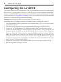
Configuring the LJ12EVB
This chapter explains how to configure the LJ12EVB development board for ISP and debugging
from a host PC using miniMON interface. LJ12EVB uses an external miniMON programmer/
debugger (miniMON-DBG). You can build your own miniMON programmer/debugger according
to free schematic from www.hc08.cz/minimon/. Here you can find useful application notes and
schematic of simple miniMON programmer/debugger.
Warning: Target board LJ12EVB is powered from +5V power supply!
Assembling the LJ12EVB target board for the MON08 mode for using with a host PC:
1. Check the miniMON-DBG configuration. Select MON08 mode and 5V-power supply output
on miniMON interface.
2. Disconnect power from the target board and miniMON debugger (miniMON-DBG).
3. Connect the LJ12EVB connector X3 with the miniMON-DBG. Use the cable provided.
4. Connect miniMON-DBG to a serial COM port on the host PC. Set up baud rate for
communication with MCU in the MON08 mode. Select correct Target Hardware
Type: e.g. Class III – Direct serial to target w/MON08 serial port circuitry build in.
Note: The communication baud rate in the MON08 mode depends on used external clock
oscillator and the state of the PTC1 pin in the time of entering the MON08 mode. Typical
external oscillator frequency is 9,83MHZ or 4,915MHz. See the MC68HC908LJ12 Technical
Data - Section 10. Monitor ROM (MON).
5. Connect the power supply. The miniMON-DBG can power the target board LJ12EVB.
6. Start the programmer/debugger software.
Starter Kit LJ12EVB
9
Pinouts
LJ12EVB Connector X2
VCC
2
1
VCC
GND
4
3
GND
PTA3
6
5
PTD0
PTA4
8
7
PTD1
PTA5
10
9
PTD2
PTA6
12
11
PTD3
PTA7
14
13
PTC7
RXD-X2
16
15
TXD-X2
LJ12EVB Connector X3 (miniMON)
OSC1
2
1
VCC
/IRQ
4
3
GND
PTA1
6
5
/RES
PTA2
8
7
PTA0
10
9
PTC1
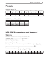
NTC/22K Parameters and Nominal
Values
NTC/22 K – BC Components, Ordering code 2322 640 6322
Temperature range ....................................-40 °C to 125 °C
Thermal cooling time constant ................ 1,2 s
Max. Power dissipation at 25 °C...............0,5 W
T is an actual temperature [K]
The resistance of the sensor at a reference temperature of 25 °C ............R25 = 22 k. ± 5 %
A material constant ..................................................................................B25,85 = 3 740 ± 2 %
T0 ............................................................................................................. 298,15
Resistance value at temperature T:
RT = R25 exp {B25,85 (1/T - 1/T0 )}
T [°C]
0
5
10
15
20
25
30
35
40
45
50
Rt [Ω] 69348 54217 42758 34000 27248 22000 17888 14643 12063 9999 8336
10
Starter Kit LJ12EVB
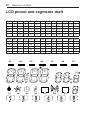
LCD pinout and segments draft
BP1
1
BP0
2
BP0
FP22 FP21 FP19 FP18 FP17 FP16 FP15 FP14 FP13 FP12 FP11
3
4
5
6
7
8
9
10
11
12
13
1F
1A
1B
2F
2A
2B
3F
3A
3B
4F
4A
1E
1G
1C
2E
2G
2C
3E
3G
3C
4E
4G
K1
1D
K2
K3
2D
P1
K4
3D
K5
K6
4D
X1
H1
X2
X3
H2
P2
X4
H3
X5
Y1
H4
FP9
15
5F
5G
5E
5D
FP8
16
5A
5B
5C
H5
BP1
FP10
14
4B
4C
K7
X6
H1
FP7
17
6F
6G
6E
6D
H2
FP6
18
6A
6B
6C
P3
FP5
19
7F
7G
7E
7D
H3
1
2
B
3
X1
BP3
25
24
BP2
26
BP2
BP3
H6
H7
4
Y2
5
6
P2
D
K1
FP1
23
8A
8B
8C
H7
H5
P1
C
�
FP2
22
8F
8G
8E
8D
Y1
G
E
FP3
21
Y2
H4
A
F
FP4
20
7A
7B
7C
H6
K2
��
K3
X2
7
P3
K4
X3
8
K5
K6
X4
K7
X5
X6
Starter Kit LJ12EVB
11
Schematic description
The basic component of the LJ12EVB target board is the microcontroller MC68HC908LJ12
from Motorola®.
The board is powered from the 5V stabilized power supply. The power input is protected against
reversing of polarity and over voltage transil NT1 TRANS/6V8. The power supply can be
connected from round connector X5, terminal X6 and miniMON connector X3. Because MCU
has integrated the real time clock module (RTC) there is a X7 connector for 3V battery backup.
In your applications you can also use the MCU low power modes WAIT or STOP. These modes
decrease the MCU current consumption and you can increase the battery life. To avoid problems
whenever the voltage is below operating level the MCU contains low voltage inhibit module.
This module monitors the voltage on the VDD pin and forces a reset when the voltage is below
LVI trip falling voltage, VTRIP. Bits LVISEL0 and LVISEL1 in the CONFIG2 register select
the value of VTRIP (see MC68HC908LJ12 datasheet). Setup 3V operating mode (LVISEL1=0,
LVISEL=1) because MCU is powered through VD2=TMMBAT46. When 5V operating mode is
selected the LVI reset can occur.
The MON08 mode is a special MCU mode for debugging and FLASH programming. The MCU
uses high voltage VTST on the IRQ pin and defined logic levels on PTA1, PTA2 and PTC1 to
enter MON08. The VTST voltage should be from 7,5V to 9V and is connected by miniMON
connector X3. When the VTST voltage is not in defined range MCU will not enter MON08
mode. The MCU needs an external clock source when in the MON08 mode. This condition is
accomplished with OSC1 signal on miniMON X7 connector. While LJ12EVB contains the clock
generator based on the 32,7 KHz crystal in MON08 mode MCU disables this crystal oscillator
and uses external clock source. Some pins uses to enter MON08 mode are shared with simple
applications on target board. PTA0 is used for communication in MON08 mode simultaneously
with VL3 LED driving. You can see LED blinking when the MCU communicates with a host
computer. Similar applications are connected to pins PTA1 and PTA2. Pin PTC1 is not connected
to user’s application when MCU is in user mode this pin is reserved for LCD driving. The MCU
needs POR reset when supply voltage is bellow 0,1V to unlock MCU FLASH in the time of
programming. The POR is generated by turn-off the switch SA15.
There is the RS232 interface (DD1 MAX202 and X4) on target board. The user application can
use the RS232 interface to communicate with the host PC. There are jumpers JP4 and JP5 to select
application for the communication interface. Because the MCU has implemented the Infrared
communication module (IRSCI) user can disconnect RS232 interface and switch RXD/TXD pins
to connector X2, prepared for external applications.
The LJ12EVB target board contains some simple peripherals like LEDs, LCD, buttons, relay
output and temperature sensor.
Pins PTB4 and PTB5 are used for LEDs driving. The LED lights when the MCU sets value 0 on
appropriate PTB pin. These pins are shared for buttons SA13 and SA14. To avoid conflict between
output and button input it is recommended to initialize pins for input and if LED should light clear
respective PTB bit and then set this pin for output. Buttons SA1 – SA12 are circuit to multiplex
12
Starter Kit LJ12EVB
connection. The application software must clear one of driving pin PTC4 – PTC6 and than read
input on PTD4 – PTD7. PTD4 to PTD7 are shared with keyboard interrupt module (KBI) so you
can use it in your application. There are two configuration bits PCEH and PCEL in the CONFIG2
register. Clear the PCEH bit to configure PTC4 – PTC7 as standard I/O pins.
On the HC908LJ12 board is also the LCD connected to the HC908LJ12 LCD driver module.
Configure LCD driver for 1⁄4 duty cycle. In this mode BP0 – BP3 are used for the LCD backplane
driving. Pins FP1 – FP22 are used for the LCD frontplane driving. Set the PCEL bit in the
CONFIG2 to configure PTC0 – PTC3 as LCD frontplane drivers FP19 – FP22. See table with
the LCD pinout and segments draft
The thermistor VR1 and R5 are used for temperature measuring. An analog voltage on the PTB6/
ADC4 pin is calculated by this formula Uad0=(Vcc/(VR1+R5))*R5. The VR1 nominal values
according to temperature are in the following table. The pin PTB7/ADC5 is wired in the connector
X6. The user’s application can use this pin as general purpose I/O pin or analog input ADC5. For
applications with digital thermometer DS1820 or compatible type set the jumper JP1.
The PTA2 pin drives the relay. To switch-on relay set PTA2 to high. The pin PTA1 drives the beeper.
The beeper sounds when the PTA1 generates square wave signal of the acoustic frequency.
Not used MCU pins are wired in the connector X2 for a special user’s applications.
Starter Kit LJ12EVB
LJ12EVB schematic diagram
13
14
Starter Kit LJ12EVB
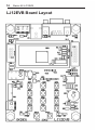
LJ12EVB Board Layout
Starter Kit LJ12EVB
15
Troubleshooting
Troubleshooting MCU power on reset (POR)
The MCU needs POR reset when supply voltage is bellow 0,1V. The POR can be generated
automatically from the miniMON debugger/programmer or manually by turn-off the SA15 switch
on the target board. It depends on the used programmer/debugger. It is not sufficient disconnect
only MCU VDD power to generate POR. The MCU can be powered from the input pins e.g. the
external oscillator.
The MCU on LJ12EVB is self-resetting
The MCU contains low voltage inhibit module. This module monitors the voltage on the VDD
pin and forces a reset when the voltage is below LVI trip falling voltage, VTRIP. Bits LVISEL0
and LVISEL1 in the CONFIG2 register select the value of VTRIP (see MC68HC908LJ12
datasheet). Setup 3V operating mode (LVISEL1=0, LVISEL=1) because MCU is powered through
VD2=TMMBAT46. When 5V operating mode is selected the LVI reset can occur.
Troubleshooting MON08 mode
l Set up correct baud rate for communication with MCU in the MON08 mode according to
used external clock oscillator and the state of the PTC1 pin in the time of entering the MON08
mode.
l The LJ12EVB emulation of the on-board MCU is limited. Port A bit 0 (PTA0) is used for
host-to-MCU communication. The port bit is not available for connection to the target system.
Setting DDRA bit 0 to 1 will stop communication with the simulation or debugger software
and will require the system reset to regain communication with the MCU.
l Check state of pins PTA0 – PTA2 and PTC1 in the time of active reset. The external miniMON
programmer/debugger have to control their state.
See miniMON description on www.hc08.cz/minimon/.
Troubleshooting HC908 Security
The HC908 MCU family contains a security mechanism for the code readout prevention based
on information that the user programs into the part. The FLASH memory content is secured by
eight-byte password, which must be sent to the MCU in time of monitor mode entering. The
password secures the FLASH memory only, other functions are accessible regardless the password
is correct or not.
The password resides in top of the FLASH (0xFFF6 – 0xFFFD), where interrupt vector table is as
well. It can be said, that the password is made automatically, when the program is compiled and
the interrupt vector table is generated. It also means, that different versions of the same software
usually have different passwords.
When the user does not need to use the FLASH (e.g. in-circuit simulation), the password is
not mandatory. The correct password enables to the user the access to the FLASH and FLASH
control, like readout its contents, erasing, programming or program running (instruction and data
fetching). The only feature not locked out by wrong password is MASS-ERASE of whole FLASH.
16
Starter Kit LJ12EVB
This is also the only way, how to regain access to the FLASH in case of unknown password.
After erasing you can enter into MON08 mode again with security bytes for blank device (FFFF-FF-FF-FF-FF-FF-FF).
Note: New versions of manual, technical documentation and application notes you can find on
www.hc08.cz.
Beta Control Ltd.
www.betacontrol.cz
www.hc08.cz