1
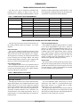
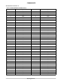
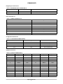
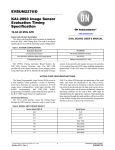
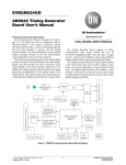
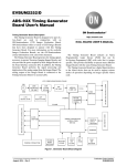
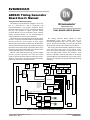
EVBUM2265/D
AD9945 Timing Generator
Board User's Manual
Timing Generator Board Description
This Timing Generator Board is designed to be used as
part of a two-board set, used in conjunction with
a ON Semiconductor CCD Imager Evaluation Board.
ON Semiconductor offers a variety of CCD Imager Boards
that have been designed to operate with this Timing
Generator Board. For more information on the available
Imager Evaluation Boards, see the ON Semiconductor
contact information at the end of this document.
The Timing Generator Board generates the timing signals
necessary to operate ON Semiconductor Imager Boards,
and also provides the power required by these Imager
Boards via the board interface connector (J6). In addition the
Timing Generator Board performs the signal processing and
digitization of the analog output of the Imager Board. Up to
two analog outputs of the Imager Board are connected to the
Timing Generator Board via coaxial cables.
The KSC−1000 Timing Generator chip provides multiple
pixel-rate, line-rate, and frame rate clocks and control
signals to operate ON Semiconductor CCD image sensors.
The KSC−1000 is able to operate many different Interline,
Full-Frame, and Linear CCD image sensors.
EVAL BOARD USER’S MANUAL
The Timing Generator Board contains an Altera
Programmable Logic Device (PLD) that can be
In-System-Programmed (ISP) with code that is imager
specific. This provides flexibility to operate many different
Imager Boards with the same Timing Generator Board.
The Timing Generator Board has a digital Input interface
to the Altera device that can be used to support various
modes of operation depending on imager-specific Altera
code. The digital input interface also includes a serial
interface to the KSC−1000 and AFE parts on the Timing
Generator Board so that adjustments may be made to their
operation, overriding the pre-programmed default operating
conditions.
JTAG
Connector
Configuration
Switches
SW[3..0]
DIO[15..0]
EPROM
3.3V
Analog
Regulator
3.3V
Digital
Regulator
1.8V
Analog
Regulator
PLD_OUT[19..0]
INTEGRATE
KSC−1000
Timing
Generator
VD, HD,
PIXEL_CLK
SERIAL TG
SLOAD TG6
SDATA, SCLK
LVDS Drivers
Hx, Vx, SHPx,
SHDx, PBLK,
INTG_START,
LINE_VALID,
FRAME_VALID,
AMP_EN
LVDS Drivers
100−pin SCSI Output Connector
Altera PLD
Board Interface Connector
SERIAL
INPUT
Power Connector
+5V, −5V, +20V, −20V
System
Clock
Oscillator
POWER_ON_DELAY
Digital Input
Buffers
DIO Input Connector
Board
Reset
Switch
http://onsemi.com
LINE_VALID, FRAME_VALID, DATACLK
CHANNEL 1
OUT[11..0]
CHANNEL 2
OUT[11..0]
SLOAD AFE1
Analog
Front End
Line Receiver
Op−Amp
SDATA, SCLK, SHPx, SHDx,
CLPOBx, PBLK
Analog
Front End
Channel 1
Video In
Line Receiver
Op−Amp
Integrate
Channel 2
Video In
SLOAD AFE2
Figure 1. 3F5592 Timing Generator Board Block Diagram
© Semiconductor Components Industries, LLC, 2014
October, 2014 − Rev. 2
1
Publication Order Number:
EVBUM2265/D
EVBUM2265/D
TIMING GENERATOR BOARD INPUT REQUIREMENTS
The input power may be supplied by standard linear
benchtop power supplies as long as they meet the
requirements of a particular Evaluation Boardset. General
guidelines for these requirements are shown in Table 1; refer
to the appropriate Timing Specification for the input power
requirements of a particular Evaluation Boardset.
Table 1. POWER SUPPLY INPUT REQUIREMENTS
Power Supplies
Minimum
Typical
Maximum
Unit
+5V_MTR Supply
4.9
5
5.1
V
800
−5V_MTR Supply
−5.1
VPLUS Supply
18
−5
mA
−4.9
V
50
mA
20
21
V
(Imager Board Dependent)
VMINUS Supply
−18
−20
mA
−21
V
(Imager Board Dependent)
mA
TIMING GENERATOR BOARD ARCHITECTURE OVERVIEW
Power-On Delay/Board Reset
The following sections describe the functional blocks of
the Timing Generator Board (See Figure 1 for a block
diagram).
The POWER_ON_DELAY signal provides a reset signal
to the Altera Programmable Logic Device (PLD) on
power-up, or when the BOARD RESET button (S1) is
pressed. The delay is generated by an RC network into
a Schmitt trigger, and is approximately 400 ms, allowing
power supply voltages to stabilize on the board. When the
POWER_ON_DELAY signal goes high, the PLD will
perform its normal power-up initialization sequence, as
detailed in the applicable Timing Specification.
Power Connector
The J7 power connector provides the necessary power
supply inputs to the Timing Generator Board. The connector
also provides the VPLUS and VMINUS power supplies.
These supplies are not used by the Timing Generator Board
but are needed by the CCD Imager Boards. The Timing
Generator Board simply routes these power supplies from
the power connector to the board interface connector.
System Clock
The System Clock is used to generate the pixel rate clocks.
The pixel rate timing signals operate at a frequency that is
divided down from the System Clock frequency. The exact
pixel rate frequency is Altera code dependent, but is limited
to 1/2 the frequency of the System clock.
Power Supply Filtering
Power supplied to the board is de-coupled and filtered
with ferrite beads and capacitors in order to suppress noise.
For best noise performance, linear power supplies should be
used to provide power to the boards.
Table 2. TIMING BOARD CLOCK RATES
Timing Board PN
System Clock
Pixel Clock (Max)
3F5592
40 MHz
20 MHz
Digital Input Connector
Any TTL-compatible digital controls may be used to
control these lines. While it is recommended that these
inputs range between +3.3 V (HIGH) and 0 V (LOW),
voltages up to +5.0 V are acceptable.
The digital input control lines to the board are buffered.
The input pins to the buffer IC’s are weakly held low by pull
down resistors to GND. Therefore, with no digital inputs, the
default level of the control lines is all zeros.
The digital input connector (J3) connects optional remote
digital control signals to the evaluation board. These control
signals, DIO[15..0], can be used to adjust the operating
mode of the evaluation board. The function of the digital
inputs depends on the Altera firmware programmed for
a particular Evaluation Boardset, and is detailed in the
associated Altera Code Timing Specification. This is an
optional feature; no external digital inputs are required for
board operation.
http://onsemi.com
2
EVBUM2265/D
Image Sensor LVDS Drivers
A three-wire serial interface is also provided on the J3
input connector. The Altera PLD is programmed to decode
the serial datastream, and steers the datastream to the
KSC−1000 and the AFE chips as necessary. Therefore the
KSC−1000 and each of the two AFE chips may be adjusted
independently of one another via the serial interface,
overriding the default settings stored in the Altera PLD. This
is an optional feature, and is not required for board
operation.
Timing signals are sent to the Imager Board via the board
interface connector (J5) using Low Voltage Differential
Signaling (LVDS) drivers. LVDS combines high-speed
connectivity with low noise and low power.
Board Interface Connector
This 80-pin connector (J5) provides both the timing
signals and the necessary power to the CCD Imager Boards
from the Timing Generator Board.
Configuration Switches
Altera PLD
There are four switches on the board that can be used to
adjust the operating mode of the Timing Generator Board.
The function of the switches depends on how the Altera
device is programmed for a particular Evaluation Boardset,
and is detailed in the associated Altera Code Timing
Specification.
The Programmable Logic Device (PLD) is an Altera Flex
10K series part. Paired with an EPC2 configuration
EPROM, the Altera device is In System Programmable
(ISP) via a 10-pin JTAG header (J4) located on the board. In
this way, the Altera device is programmed with
imager-specific code to operate the Imager Board to which
the Timing Generator Board will be connected.
The code implemented in the Altera PLD is specific to
each CCD Imager Board configuration, and is detailed in the
associated Timing Specification document. At a minimum,
the Altera PLD must provide these functions:
• Decode and steer serial input data to the correct device;
• Program the KSC−1000 with default settings;
• Program the AFE chips with default settings.
JTAG Header
This 10-pin header (J4) provides the user with the ability
to reprogram the Altera PLD in place via Altera’s
BYTEBLASTER programming hardware.
Purchasers of a ON Semiconductor Evaluation Board Kit
may, at their discretion, make changes to the Altera code
firmware. ON Semiconductor Inc. can only support
firmware developed and supplied by ON Semiconductor
Inc. Changes to the Altera code firmware are at the risk of
the customer.
When programming the Altera PLD via the JTAG
interface, the Imager Board must be disconnected from the
Timing Board, by removing the Board Interface Cable
before power is applied. If the Imager Board is connected to
the Timing Board during the reprogramming of the Altera
PLD, damage to the Imager Board may occur.
In addition to these functions, the Altera PLD may provide
auxiliary timing and control functions for a particular CCD
Imager Board. Refer to the appropriate Timing
Specification for details.
Serial Input Steering
When the three-wire serial input to the Timing Board is
used, the Altera PLD decodes the addressing of the serial
input, and steers the datastream to the correct device.
The serial input must be formatted so that the Altera PLD
can correctly decode and steer the data to the correct device.
The first 3 bits in the datastream are the Device Select bits
DS[2..0], sent MSB first, as shown in Figure 2. The Device
Select bits are decoded as shown in Table 3.
Integrate Output Connector
This output header (J6) provides a signal that is high
during the integration time period. INTEGRATE can be
used to synchronize an external shutter or LED light source
with the integration time period.
Table 3. SERIAL INPUT DEVICE SELECT
Device Select DS[2..0]
Serial Device
000
PLD
001
AFE1
010
AFE2
011
KSC−1000
100
(Imager Board Dependent)
101
(Imager Board Dependent)
110
(Imager Board Dependent)
111
(Imager Board Dependent)
http://onsemi.com
3
EVBUM2265/D
SLOAD
SDATA
…
Dn
Address bits A[2..0], LSB first, followed by a Test bit which
is always set LOW.
The remaining bits in the bitstream are Data bits, LSB
first, with as many bits as are required to fill the appropriate
register.
DS2
DS1
DS0
R/W
A0
A1
A2
A3 (or Test)
D0
D1
D2
D3
D4
The next bit in the datastream is the Read/Write bit (R/W).
Only writing is supported; therefore this bit is always LOW.
The definition of next four bits in the datastream depends
on the device being addressed with the Device Select bits.
For the KSC−1000 device, they are Register Address bits
A[3..0], LSB first. For the AD9945 AFE, they are Register
ÏÏÏÏÏÏÏÏÏÏÏÏÏÏ
ÏÏÏÏÏÏÏÏÏÏÏÏÏÏ
SCLK
Figure 2. Serial Input Timing
three-wire serial interface. The default settings are specific
to each CCD Imager Board configuration, and are detailed
in the associated Timing Specification document.
The Altera PLD receives the serial datastream, decodes
the Device Select address contained in the first 3 bits, and
sets the appropriate SLOAD line LOW. The remaining
datastream is then read in real time by the selected device.
The Altera PLD does not do any checking of the datastream
for correctness; it merely steers the data to the appropriate
device.
AFE Default Programming
Upon power-up, or whenever the BOARD_RESET
button is pressed, the Altera PLD programs the registers of
the two AFE chips on the AFE Timing Generator Board to
their default settings via the three-wire serial interface.
The default settings are specific to each CCD Imager Board
configuration, and are detailed in the associated Timing
Specification document.
KSC−1000 Default Programming
Upon power-up, or whenever the BOARD_RESET
button is pressed, the Altera PLD automatically programs
the registers of the KSC−1000 to their default settings via the
Table 4. TIMING BOARD CONFIGURATION OPTIONS
Timing Board PN
Analog Devices PN
Sampling Rate
Bit Depth
Channels
3F5592
AD9945KCP
20 MSPS
12
2
Video Signal Processing
Auxiliary PLD functions
The Altera PLD may provide auxiliary timing and control
functions for a particular CCD Imager Board. In addition to
the Configuration switches, Remote Digital Inputs, and
3-wire Serial Interface, the inputs to the PLD include timing
signals from the KSC−1000. The PLD outputs include:
PLD[2..0], auxiliary outputs which are routed to the Board
Interface connector (J5); HD_TG and VD_TG, timing
controls signals to the KSC−1000; and ARSTZ,
an asynchronous reset to the KSC−1000. These inputs and
outputs allow the Altera PLD to monitor the CCD timing,
and to control auxiliary functions as needed.
There are several PLD connections that are connected
only to test points. These may be configured as PLD outputs
or inputs, for extra monitoring or control.
Each of the two signal processing channels is designed to
process an analog video signal input from a CCD Imager
Board. The analog video signal is buffered by an operational
amplifier. This amplifier is in a non-inverting
configuration with a gain of 1.25.
The output of the amplifier is then AC-coupled into the
input of the AFE chip. Since the amplitude of AFE input is
limited, care must be taken to adjust the gain of the Imager
Board signal prior to the AFE input. The Imager Board for
a particular CCD image sensor has been designed to deliver
a video signal with the correct amplitude to the Timing
Board, such that, when the AFE is correctly configured,
optimum performance is achieved.
http://onsemi.com
4
EVBUM2265/D
AD9945 Analog Front End (AFE) Device
The Timing Generator Board has two analog input
channels, each consisting of an operational amplifier buffer
and an Analog Front End (AFE) device. The AFE chip
processes the video signal, then performs the A/D
conversion and outputs 12 bits of digital information per
pixel. The Timing Generator Board supports the AD9945
AFE device offered by Analog Devices Inc.
Refer to the Analog Devices AD9945 Specification Sheet
(Reference 2) for details on the operation of this Analog
Front End.
Table 5. AFE REGISTERS
Register Address
Register Description
Notes
0
Operation
1
1
Control
1
2
Clamp Level
1
3
VGA Gain
1
1. See the AD9945 specifications sheet (Reference 2) for details.
frame-grabber hardware. The output connector interfaces
directly to the National Instruments PCI−1424
frame-grabber, providing two channels of 12 bit output data
in parallel in LVDS differential format. The connector also
provides the three necessary PCI−1424 frame grabber
synchronization signals in LVDS differential format.
The AFE registers can be adjusted by re-programming the
registers using the three-wire serial interface provided on the
Digital Input Connector. Each AFE is independently
addressable through the Altera PLD, and therefore can be
adjusted independently.
Digital Image Data LVDS Drivers
Digitized image data and synchronization timing signals
are sent to the computer frame-grabber hardware via the
100-pin SCSI output connector (J9) using Low Voltage
Differential Signaling (LVDS) drivers. LVDS combines
high-speed connectivity with low noise and low power.
KSC−1000 Timing Generator
The KSC−1000 controls the overall flow of the evaluation
board operation. The TG outputs include the CCD clocks
signals, AFE timing signals, and Frame Grabber
synchronization signals. The KSC−1000 is configured by
programming Registers, Frame Tables, and Line Tables.
SCSI Digital Output Connector
This 100-pin connector (J9) provides digitized image data
and synchronization timing signals to the computer
Table 6. KSC−1000 REGISTERS
Register Address
Register Description
Notes
0
Frame Table Pointer
1
1
General Setup
1
2
General Control
1
3
INTG_STRT Setup
1
4
INTG_STRT Line
1
5
Signal Polarity
1
6
Offset
1
7
Width
1
8
Frame Table Access
1
9
Line Table Access
1
10
Status
1
1. See the KSC−1000 specification sheet (Reference 3) for details.
http://onsemi.com
5
EVBUM2265/D
CONNECTOR ASSIGNMENTS AND PINOUTS
SMB Connectors J1 and J2
J1 (Channel 1) and J2 (Channel 2) allow connection of
analog video signal(s) from the CCD Imager Boards through
correctly terminated 75 W coaxial cable.
Digital Input Connector J3
Table 7. DIGITAL INPUT CONNECTOR J3
Pin
Assignment
Function
Pin
Assignment
1
SLOAD
SERIAL PORT
2
GND
3
SDATA
SERIAL PORT
4
GND
5
SCLOCK
SERIAL PORT
6
GND
7
DIO15
Altera Code Dependent
8
GND
9
DIO14
Altera Code Dependent
10
GND
11
DIO13
Altera Code Dependent
12
GND
13
DIO12
Altera Code Dependent
14
GND
15
DIO11
Altera Code Dependent
16
GND
17
DIO10
Altera Code Dependent
18
GND
19
DIO9
Altera Code Dependent
20
GND
21
DIO8
Altera Code Dependent
22
GND
23
DIO7
Altera Code Dependent
24
GND
25
DIO6
Altera Code Dependent
26
GND
27
DIO5
Altera Code Dependent
28
GND
29
DIO4
Altera Code Dependent
30
GND
31
DIO3
Altera Code Dependent
32
GND
33
DIO2
Altera Code Dependent
34
GND
35
DIO1
Altera Code Dependent
36
GND
37
DIO0
Altera Code Dependent
38
GND
39
NC
(Not Used)
40
GND
JTAG Connector J4
Table 8. JTAG CONNECTOR
Pin
Assignment
1
TCK
2
AGND
3
TDO
4
+3.3 V
5
TMS
6
AGND
7
AGND
8
AGND
9
TDI
10
AGND
http://onsemi.com
6
EVBUM2265/D
Board Interface Connector J5
Table 9. BOARD INTERFACE CONNECTOR J5
Pin
Assignment
Pin
Assignment
1
TIMING_OUT0+
2
TIMING_OUT0−
3
AGND
4
AGND
5
TIMING_OUT1+
6
TIMING_OUT1−
7
AGND
8
AGND
9
TIMING_OUT2+
10
TIMING_OUT2−
11
AGND
12
AGND
13
TIMING_OUT3+
14
TIMING_OUT3−
15
AGND
16
AGND
17
TIMING_OUT4+
18
TIMING_OUT4−
19
AGND
20
AGND
21
TIMING_OUT5+
22
TIMING_OUT5−
23
AGND
24
AGND
25
TIMING_OUT6+
26
TIMING_OUT6−
27
AGND
28
AGND
29
TIMING_OUT7+
30
TIMING_OUT7−
31
AGND
32
AGND
33
TIMING_OUT8+
34
TIMING_OUT8−
35
AGND
36
AGND
37
TIMING_OUT9+
38
TIMING_OUT9−
39
AGND
40
AGND
41
TIMING_OUT10+
42
TIMING_OUT10−
43
AGND
44
AGND
45
TIMING_OUT11+
46
TIMING_OUT11−
47
N.C.
48
N.C.
49
AGND
50
AGND
51
TIMING_OUT12+
52
TIMING_OUT12−
53
−20 V_IMG
54
−20 V_IMG
55
TIMING_OUT13+
56
TIMING_OUT13−
57
AGND
58
AGND
59
TIMING_OUT14+
60
TIMING_OUT14−
61
−5 V_MTR
62
−5 V_MTR
63
TIMING_OUT15+
64
TIMING_OUT15−
65
AGND
66
AGND
67
TIMING_OUT16+
68
TIMING_OUT16−
69
+5 V_MTR
70
+5 V_MTR
71
TIMING_OUT17+
72
TIMING_OUT17−
73
AGND
74
AGND
75
TIMING_OUT18+
76
TIMING_OUT18−
77
+20 V_IMG
78
+20 V_IMG
79
TIMING_OUT19+
80
TIMING_OUT19−
http://onsemi.com
7
EVBUM2265/D
Integrate Sync Connector J6
Table 10. INTEGRATE SYNC CONNECTOR J6
Pin
Assignment
Function
1
INTEGRATE
Signal is High during Integration Time Period
2
AGND
Power Connector J7
Table 11. POWER CONNECTOR J7
Pin
Assignment
1
VMINUS
2
AGND
3
VPLUS
4
AGND
5
−5 V_MTR
6
AGND
7
+5 V_MTR
8
AGND
Configuration Switches S2
Table 12. CONFIGURATION SWITCHES S2
Switch
Assignment
Function
S2−1
SW1
Altera Code Dependent
S2−2
SW2
Altera Code Dependent
S2−3
SW3
Altera Code Dependent
S2−4
SW4
Altera Code Dependent
Output Connector J9
Table 13. OUTPUT CONNECTOR J9
Pin
Assignment
Signal Level
Pin
Assignment
Signal Level
1
AOUT0+
LVDS
2
AOUT0−
LVDS
3
AOUT1+
LVDS
4
AOUT1−
LVDS
5
AOUT2+
LVDS
6
AOUT2−
LVDS
7
AOUT3+
LVDS
8
AOUT3−
LVDS
9
AOUT4+
LVDS
10
AOUT4−
LVDS
11
AOUT5+
LVDS
12
AOUT5−
LVDS
13
AOUT6+
LVDS
14
AOUT6−
LVDS
15
AOUT7+
LVDS
16
AOUT7−
LVDS
17
AOUT8+
LVDS
18
AOUT8−
LVDS
19
AOUT9+
LVDS
20
AOUT9−
LVDS
21
AOUT10+
LVDS
22
AOUT10−
LVDS
23
AOUT11+
LVDS
24
AOUT11−
LVDS
25
N.C.
26
N.C.
http://onsemi.com
8
EVBUM2265/D
Table 13. OUTPUT CONNECTOR J9 (continued)
Pin
Assignment
27
Signal Level
Pin
Assignment
Signal Level
N.C.
28
N.C.
29
N.C.
30
N.C.
31
N.C.
32
N.C.
33
N.C.
34
N.C.
35
N.C.
36
N.C.
37
N.C.
38
N.C.
39
N.C.
40
N.C.
41
FRAME+
LVDS
42
FRAME−
LVDS
43
LINE+
LVDS
44
LINE−
LVDS
45
N.C.
46
N.C.
47
N.C.
48
N.C.
49
PIXEL+
LVDS
50
PIXEL−
LVDS
51
BOUT0+
LVDS
52
BOUT0−
LVDS
53
BOUT1+
LVDS
54
BOUT1−
LVDS
55
BOUT2+
LVDS
56
BOUT2−
LVDS
57
BOUT3+
LVDS
58
BOUT3−
LVDS
59
BOUT4+
LVDS
60
BOUT4−
LVDS
61
BOUT5+
LVDS
62
BOUT5−
LVDS
63
BOUT6+
LVDS
64
BOUT6−
LVDS
65
BOUT7+
LVDS
66
BOUT7−
LVDS
67
BOUT8+
LVDS
68
BOUT8−
LVDS
69
BOUT9+
LVDS
70
BOUT9−
LVDS
71
BOUT10+
LVDS
72
BOUT10−
LVDS
73
BOUT11+
LVDS
74
BOUT11−
LVDS
75
N.C.
76
N.C.
77
N.C.
78
N.C.
79
N.C.
80
N.C.
81
N.C.
82
N.C.
83
N.C.
84
N.C.
85
N.C.
86
N.C.
87
N.C.
88
N.C.
89
N.C.
90
N.C.
91
N.C.
92
N.C.
93
N.C.
94
N.C.
95
N.C.
96
N.C.
97
N.C.
98
N.C.
99
AGND
100
AGND
http://onsemi.com
9
EVBUM2265/D
WARNINGS AND ADVISORIES
Board during the reprogramming of the Altera PLD, damage
to the Imager Board will occur.
Purchasers of a ON Semiconductor Evaluation Board Kit
may, at their discretion, make changes to the Timing
Generator Board firmware. ON Semiconductor can only
support firmware developed by, and supplied by,
ON Semiconductor. Changes to the firmware are at the risk
of the customer.
ON Semiconductor is not responsible for customer
damage to the Timing Board or Imager Board electronics.
The customer assumes responsibility and care must be taken
when probing, modifying, or integrating the
ON Semiconductor Evaluation Board Kits.
When programming the Timing Board, the Imager Board
must be disconnected from the Timing Board before power
is applied. If the Imager Board is connected to the Timing
ORDERING INFORMATION
ON Semiconductor reserves the right to change any
information contained herein without notice. All
information furnished by ON Semiconductor is believed to
be accurate.
Please address all inquiries and purchase orders to:
Truesense Imaging, Inc.
1964 Lake Avenue
Rochester, New York 14615
Phone: (585) 784−5500
E-mail: [email protected]
ON Semiconductor and the
are registered trademarks of Semiconductor Components Industries, LLC (SCILLC) or its subsidiaries in the United States and/or other countries.
SCILLC owns the rights to a number of patents, trademarks, copyrights, trade secrets, and other intellectual property. A listing of SCILLC’s product/patent coverage may be accessed
at www.onsemi.com/site/pdf/Patent−Marking.pdf. SCILLC reserves the right to make changes without further notice to any products herein. SCILLC makes no warranty, representation
or guarantee regarding the suitability of its products for any particular purpose, nor does SCILLC assume any liability arising out of the application or use of any product or circuit, and
specifically disclaims any and all liability, including without limitation special, consequential or incidental damages. “Typical” parameters which may be provided in SCILLC data sheets
and/or specifications can and do vary in different applications and actual performance may vary over time. All operating parameters, including “Typicals” must be validated for each
customer application by customer’s technical experts. SCILLC does not convey any license under its patent rights nor the rights of others. SCILLC products are not designed, intended,
or authorized for use as components in systems intended for surgical implant into the body, or other applications intended to support or sustain life, or for any other application in which
the failure of the SCILLC product could create a situation where personal injury or death may occur. Should Buyer purchase or use SCILLC products for any such unintended or
unauthorized application, Buyer shall indemnify and hold SCILLC and its officers, employees, subsidiaries, affiliates, and distributors harmless against all claims, costs, damages, and
expenses, and reasonable attorney fees arising out of, directly or indirectly, any claim of personal injury or death associated with such unintended or unauthorized use, even if such claim
alleges that SCILLC was negligent regarding the design or manufacture of the part. SCILLC is an Equal Opportunity/Affirmative Action Employer. This literature is subject to all applicable
copyright laws and is not for resale in any manner.
PUBLICATION ORDERING INFORMATION
LITERATURE FULFILLMENT:
Literature Distribution Center for ON Semiconductor
P.O. Box 5163, Denver, Colorado 80217 USA
Phone: 303−675−2175 or 800−344−3860 Toll Free USA/Canada
Fax: 303−675−2176 or 800−344−3867 Toll Free USA/Canada
Email: [email protected]
N. American Technical Support: 800−282−9855 Toll Free
USA/Canada
Europe, Middle East and Africa Technical Support:
Phone: 421 33 790 2910
Japan Customer Focus Center
Phone: 81−3−5817−1050
http://onsemi.com
10
ON Semiconductor Website: www.onsemi.com
Order Literature: http://www.onsemi.com/orderlit
For additional information, please contact your local
Sales Representative
EVBUM2265/D