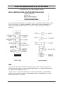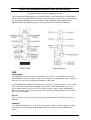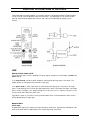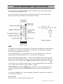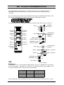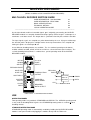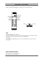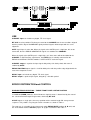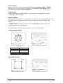
1
TIMS ADVANCED MODULES and
TIMS SPECIAL APPLICATIONS MODULES
USER MANUAL
Telecommunications Instructional Modelling System
TIMS ADVANCED MODULES and TIMS SPECIAL APPLICATION MODULES
USER MANUAL
Authors: Alfred Breznik and Carlo Manfredini
Issue Number 3.9 June 2008
All specifications are subject to change without notice.
Published by:
EMONA INSTRUMENTS PTY LTD
a.c.n. 001 728 276
86 Parramatta Road
Camperdown NSW 2050
Sydney AUSTRALIA
web: www.tims.com.au
telephone: +61-2-9519-3933
fax:+61-2-9550-1378
Copyright (C) 1988 - 2008 Emona Instruments Pty Ltd and its related entities. All rights
reserved. No part of this publication may be reproduced, distributed or translated in any form or
by any means, including any network or Web distribution or broadcast for distance learning, or
stored in any database or in any network retrieval system, without the prior written consent of
Emona Instruments Pty Ltd.
For licensing information, please contact Emona Instruments Pty Ltd.
The TIMS logo
Printed in Australia
is a registered trademark of Emona TIMS Pty Ltd.
CONTENTS
Part I TIMS INTRODUCTION
TIMS OVERVIEW
SYSTEM CONVENTIONS
Front Panel Sockets and Labelling
Advanced Module Set Number 1 Module List
Part II ADVANCED MODULES USER INSTRUCTIONS
Baseband Channel Filters
Decision Maker
Delta Modulation Utilities
Delta Demodulation Utilities
Error Counting Utilities
Line Code & Partial Response Encoder
Line Code & Partial Response Decoder
Noise Generator
Wideband True RMS Volt Meter
100kHz Channel Filters
Spectrum Analyser Utilities
PCM Encoder
PCM Decoder
Block Code Encoder
Block Code Decoder
Convolutional Code Encoder
Convolutional Code Decoder
Integrate & Dump
Trellis Code Modulation Decoder
Bit Clock Regeneration
FM Utilities
M-Level Encoder
M-Level Decoder
Digital Utilities
Quadrature Utilities
Speech Module
Multiple Sequences Source
CDMA Decoder
TIMS SONET/SDH Overview
TIMS STS-1 Multiplexer
TIMS STS-1 Demultiplexer
TIMS STS-3 Multiplexer
TIMS STS-3 Demultiplexer
TIMS STS Clock Regeneration
FHSS Frequency Synthesizer
Digital Error Channel
Laplace
z-Transform
MSK, OQPSK, π/4-DQPSK Module
UWB - Ultra Wideband Pulse Generator
Part III SPECIAL APPLICATIONS MODULES USER INSTRUCTIONS
100kHz Tx Antenna
100kHz Rx Antenna Utilities
Fibre Optic Transmitters
Fibre Optic Receiver
Fiber Optic Coupler
Fiber Optic WDM Filters
1
2
3
4
6
12
18
22
25
30
32
33
34
35
38
43
46
49
53
62
67
71
78
81
83
87
96
97
98
100
103
106
108
112
115
119
122
124
127
130
133
135
140
SA
SA
SA
SA
SA
SA
-
1
2
4
6
7
8
TIMS INTRODUCTION
TIMS OVERVIEW
TIMS is a telecommunications modelling system. It models mathematical equations
representing electrical signals, or block diagrams representing telecommunications systems.
TIMS is primarily a hands-on rather than demonstration style teaching system, which combines
both the theoretical and practical aspects of implementing systems. We are confident that TIMS
will provide the student with a clearer understanding of the concepts behind telecommunications
theory.
Physically, TIMS is a dual rack system. The top rack accepts up to 12 Eurocard sized,
compatible "black boxes", or modules. The lower rack houses a number of fixed modules, as
well as the system power supply.
The modules are very simple electronic circuits, which function as basic communications
building blocks. Each module, fixed or plug-in, has a specific function; basic functions fall into
three general categories:
Signal Generation - oscillators, etc
Signal Processing - multipliers, filters, etc
Signal Measurement - frequency counter
Modules are patched together via the front panel sockets using interconnecting leads, to model
the system under investigation.
TIMS OPTIONAL ADVANCED MODULES
The TIMS Advanced Modules add to the range and depth of experiments that can be carried
out by students and lecturers on the TIMS system. These Advanced Modules fall into two main
groups:
Digital Signal Processing - TMS320C50 and TMS320C6713 based
Specialised Modules - with specific building block functions
This manual covers a particular group of optional Specialised Modules only.
TIMS AMS1 User Manual 1
SYSTEM CONVENTIONS
All TIMS modules conform to the following mechanical and electrical conventions.
A - FRONT PANEL SOCKETS
Signal interconnections are made via front panel, 4mm sockets
Sockets on the LEFT HAND SIDE are for signal INPUTS.
All inputs are high impedance, typically 56k ohms.
Sockets on the RIGHT HAND SIDE are for signal OUTPUTS.
All outputs are low impedance, typically 330 ohms.
YELLOW sockets are only for ANALOG signals.
ANALOG signals are held near the TIMS standard reference level of 4V pk-pk.
RED sockets are only for DIGITAL signals.
DIGITAL signals are TTL level, 0 to 5 V.
GREEN sockets are all common, or system GROUND.
Note that input and output impedances are intentionally mismatched, so that signal connections
may be made or broken without changing signal amplitudes at module outputs.
B - PLUG-IN MODULES
Any plug-in module may be placed in any of the 12 positions of the upper rack. All modules use
the back plane bus to obtain power supply : only the DST modules (not part of the BASIC
SYSTEM) use the bus to transfer signals. The modules are designed so that they may be
plugged-in or removed at any time, without turning off the system power. The modules are not
locked into position and may need to be held while interconnecting leads are removed.
C - LABELLING
All modules are identified as to the function they perform.
Inputs, outputs, controls and switches are labelled so that a student who has had only a brief
introduction to TIMS can use the modules without needlessly referring back to this USER
MANUAL.
It should be noted that no variable controls have calibration marks. This is intentional, as the
philosophy behind TIMS is that students setup and adjust systems by observing and measuring
signals. This assists the student in gaining a much greater understanding, feel and insight into
the operation of a communications implementation.
TIMS AMS1 User Manual 2
D - ADVANCED MODULES LIST
Below are listed all the TIMS ADVANCED MODULES.
Baseband Channel Filters
Decision Maker
Delta Modulation Utilities
Delta Demodulation Utilities
Error Counting Utilities
Line-Code & Partial Response Encoder
Line-Code & Partial Response Decoder
Noise Generator
True RMS Volt Meter
100kHz Passband Channel Filter
Spectrum Analyser Utilities
PCM Encoder
PCM Decoder
Block Code Encoder
Block Code Decoder
Convolutional Code Encoder
Convolutional Code Decoder
Integrate & Dump
Trellis Code Modulation Decoder
Bit Clock Regeneration
FM Utilities
M-Level Encoder
M-Level Decoder
Digital Utilities
Quadrature Utilities
Speech Module
Multiple Sequences Source
CDMA Decoder
TIMS STS-1 Multiplexer
TIMS STS-1 Demultiplexer
TIMS STS-3 Multiplexer
TIMS STS-3 Demultiplexer
TIMS STS Clock Regeneration
FHSS Frequency Synthesizer
Digital Error Channel
Laplace
z-Transform
MSK, OQPSK, π/4-DQPSK Module
UWB Ultra Wideband Pulse Generator
E - SPECIAL APPLICATIONS MODULE LIST
Below are listed all the TIMS SPECIAL APPLICATIONS MODULES.
100kHz Tx Antenna
100kHz Rx Antenna Utilities
Fibre Optic Transmitter (red)
Fibre Optic Transmitter (green)
Fibre Optic Receiver
Fibre Optic Coupler
Fibre Optic WDM Filters
TIMS AMS1 User Manual 3
BASEBAND CHANNEL FILTERS
(PULSE SHAPING FILTERS)
Four switch selectable, baseband channels are provided, comprising three different filters and
one straight-through connection. Each of the three filters has a stop-band frequency of near
4kHz.
USE
Only one channel may be selected and used at a time.
Note that each of the four channels may be AC or DC coupled by front panel toggle switch.
CHANNEL CHARACTERISTICS
Before using any of these four channels in experiments, each channel should be characterised
by actual measurement of amplitude and phase responses. As a minimum, the cut-off and
stop-band frequencies should be measured, using the AUDIO OSCILLATOR and TRUE RMS
METER modules or an oscilloscope.
COMPARISONS
AMPLITUDE AND PHASE VERSUS FREQUENCY
It is useful to compare the amplitude and phase response of each channel with the 7th order
elliptic TUNEABLE LOWPASS FILTER module (a standard module from of the BASIC
MODULE SET). Compare against the same cut-off frequency by adjusting the TUNEABLE
LOWPASS FILTER’s cut-off frequency to match each channel’s cut-off frequency.
EYE DIAGRAMS
Observing the EYE DIAGRAMS of digital data signals passing through the above selection of
filters will illustrate each filter’s (hence, channel’s) performance.
TIMS AMS1 User Manual 4
BASIC SPECIFICATIONS
Input coupling AC or DC, channels 1 to 4
Channel responses
Channel 1 straight-through
Channel 2 Butterworth, 7th order
Channel 3 Bessel, 7th order
Channel 4 OpFil Linear Phase *, 7th order
Stop-band attenuation approx 40dB, 4kHz
Passband ripple 0.5dB
* OpFil Linear Phase filter is a proprietary filter design having a sharp roll-off characteristic with
a linear phase response in the passband. This filter was designed by Optimum Filters Pty Ltd,
Sydney, Australia.
TIMS AMS1 User Manual 5
DECISION MAKER
DECISION MAKER SECTION GUIDE
USER INFORMATION
6
BASIC SPECIFICATIONS
8
TECHNICAL DETAILS
9
* QUICK OPERATION GUIDE
10
_________________________________________________________
Digital signals may become corrupted by noise and interference in the communications channel.
After demodulation or receiver filtering, a corrupted digital signal would need to be squared and
converted to a clean digital waveform with an associated in phase bit clock, so that further
digital processing, decoding or message recovery can be performed. The tasks of squaring the
corrupted digital signal and aligning the bit clock can be carried out by the DECISION MAKER
module.
The DECISION MAKER module accepts up to two TTL, unipolar or bipolar level, baseband
digital signals and a synchronised bit clock. The input signals are sampled at a point
determined by the user and are output as clean digital signals, along with an in-phase and
synchronised bit clock. Using an oscilloscope, the decision point is displayed as a bright marker
on the input digital waveform.
USE
INPUTS IN1 & IN2
IN1 and IN2 will each accept an incomming digital signal. If only one digital signal is available,
then either input may be used: leave the unused input unconnected. When a digital signal is
connected to each input, then both signals must have the same waveform format. Ensure the
amplitudes of the input digital signals are within TIMS standard limits of +/-2V bipolar, +2V & 0V
unipolar and +5V & 0V TTL.
TIMS AMS1 User Manual 6
WAVEFORM FORMAT SELECTION
The correct waveform format must be selected prior to using the DECISION MAKER MODULE.
The user has a choice of eight bipolar and unipolar waveforms (Line-Codes) as well as
standard TTL waveforms.
Set switch SW1 to the required waveform format position. SW1 is a PCB mounted, ten position
rotary switch at the rear of the module.
BIT CLOCK and OUTPUTS OUT1 & OUT2
This DECISION MAKER module primarily operates with bit clocks of around 2kHz. The input bit
clock, B.CLK, must be synchronised to the input digital signal(s) and so should be either
regenerated from an input digital signal or may be "stolen" from the transmitter.
The output bit clock, B.CLK, is synchronised and aligned with the output bit stream(s) in the
following manner: each new bit occurs on the negative (falling) B.CLK edges. The position of
the output bit clock’s negative edge is determined by the DECISION POINT control.
DECISION POINT CONTROL
The DECISION POINT is the point at which the incomming digital data is sampled. At the
sampling time, a decision is made as to whether the sample is "HI" or "LO" and the result is
output to the corresponding output, OUT1 or OUT2.
If a digital signal is present at each input, then both are sampled simultaneously: the results are
also output simultaneously.
The user has direct control over the position of the DECISION POINT across the bit width. The
threshold voltages for the decision are set by fixed resistors. The threshold voltages are listed
in TABLE DMK-1. See TECHNICAL DETAILS SECTION for more information.
With an input bit clock of 2kHz, the DECISION POINT can be moved continuously across more
than 90% of the bit width. The DECISION POINT can be moved by either front panel control
(INTernal control) or by external DC voltage applied to input Vin, (EXTernal control). Sliding
switch SW2, located on the PCB, selects INTernal or EXTernal control mode.
The DECISION POINT can be displayed on an oscilloscope as a bright marker, by viewing the
input digital waveform and connecting the Z-MODULATION output to the ’scope.
The DECISION POINT always moves with respect to the input bit clock. So in order to see the
bright DECISION POINT marker move across the digital waveform or EYE DIAGRAM, then the
’scope MUST be triggered by either the input sequence’s SYNC or by the INPUT bit clock.
SPECIAL NOTE
The RZ and Biphase Line-Codes may be refered to as "HALF WIDTH" waveforms, while the
other Line-Codes including TTL would be refered to as "FULL WIDTH" waveforms. Care must
be taken when moving the DECISION POINT across the "HALF WIDTH" waveforms, as only
half the "bit width" usually carries useful information. In the "HALF WIDTH" case, determining
which half of the bit width the DECISION POINT has been positioned can seen by observing
the Bit Error Rate or by viewing the actual input waveform, rather than by the EYE DIAGRAM.
See TABLE DMK-1 for the list of waveforms and their width description.
TIMS AMS1 User Manual 7
Table DMK-1 lists the supported waveforms, their thresholds, output levels and bit width
descriptions.
WAVEFORM
FORMAT SELECTED
NRZ-TTL
NRZ-L
NRZ-M
UNI-RZ
BIP-RZ
RZ-AMI
BiO-L
DICODE
DUOBINARY
THRESHOLDS
OUTPUT
LEVEL
V+
VO
VO
V+
V+, VV+, VVO
V+, VV+, V-
0, +5v
+/- 2V
+/- 2V
0, +2V
0, +/- 2V
0, +/- 2V
+/- 2V
0, +/- 2V
0, +/- 2V
CODE
BIT WIDTH
DESCRIPTION
FULL
FULL
FULL
HALF
HALF
HALF
HALF
FULL
FULL
TABLE DMK-1
Default threshold settings are: V+ = approx 1V; V- = approx -1V; VO = approx 0V
Z-MODULATION OUTPUT
The Z-MODULATION output provides a pulse at the DECISION POINT. These pulses may be
viewed on the ’scope screen or may be connected to the ’scope’s Z-modulation input. Refer to
the TECHNICAL DETAILS SECTION regarding setting-up Z-modulation, if required.
BASIC SPECIFICATIONS
Digital waveform inputs two, IN1 and IN2
Digital waveform outputs two, OUT1 and OUT2
Input/Output levels depend upon the waveform format selected:
TTL : +5V, 0V
Unipolar : +2V, 0V
Bipolar : +/-2V
Waveform format selection by 10 position rotary switch, SW1
Waveform formats supported NRZ-TTL, NRZ-L, NRZ-M, UNI-RZ, BIPOLAR-RZ, RZ-AMI,
BIPHASE-L, DICODE, DUOBINARY
Bit Clock input, B.CLK TTL level, nominally 2kHz;
operational 250Hz to 3.5kHz, performance not specified
Bit Clock output, B.CLK synchronised to the OUTput waveform; negative Bit Clock edge
aligned with each new output bit
Decision point span > 90% of bit width, with 2kHz B.CLK
DECISION POINT control selection INTernal or External, by switch SW2
DECISION POINT control continuous, by front panel knob (INT),
or, 0 to 5V DC EXTERNAL input signal (EXT) at Vin
Z-MODULATION level three modes available, with variable level control (see Technical Details)
Z-MODULATION pulse width 2uS typical
TIMS AMS1 User Manual 8
TECHNICAL DETAILS
Z-MODULATION
Three Z-modulation modes are supported, with variable level control. Each mode is selected by
positioning jumper, J1. Trimmer, RV2, controls the level of the output signal.
MODE A (position J1A)
normal intensity: +5V
bright intensity: 0V
MODE B (position J1B)
normal intensity: 0V
bright intensity: -5V
MODE C (postition J1-C)
normal intensity: 0V
bright intensity: +5V
In each case, trimmer RV2 will control the level of the "bright intensity".
DECISION POINT THRESHOLDS
The three voltage thresholds V+, V- and VO are set by fixed resistors. These can be changed if
required, for specific applications, as follows,
V+ = 15 x (R2)/(R2 + R5)
default values R2 = 10kR, R5 = 680R
V- = -15 x (R6)/(R6 + R3)
default values R3 = 10kR, R6 = 680R
VO = 15 x (R4)/(R4 + R1)
default values R1 = 56kR, R4 = 100R
BIT CLOCK
The DECISION MAKER module was specifically designed to operate with the TIMS standard
2.083kHz available from the MASTER SIGNALS module. The 2.083kHz sinewave must be
converted to TTL using the UTILITIES module’s COMPARATOR. Alternatively, the 8.33kHz
TTL signal can be divided by 4 using the LINE-CODE ENCODER module.
Other clock rates will function but the DECISION POINT adjustment range will be affected. If
the clock is increased, then the range will not extend across the full bit width. Conversely, if the
clock is decreased, the range will extend across neighbouring bit widths and become
unspecified.
TIMS AMS1 User Manual 9
QUICK OPERATION GUIDE
A - Viewing the operation of the DECISION MAKER
For example, a SEQUENCE GENERATOR and TUNEABLE LOWPASS FILTER as the source
of a "corrupted" digital stream make an ideal demonstration signal.
1. Select the appropriate digital waveform being used for the experiment, at rotary switch SW1,
which is located at the rear of the module.
2. Select the correct Z-modulation mode to suit your oscilloscope (See TECHNICAL DETAILS
section on setting-up Z-modulation).
3. Select INT at DECISION switch, SW2, near the front of the module.
4. Connect the digital signal to IN1 and the bit clock to B.CLK input.
5. Connect the oscilloscope’s EXTERNAL trigger input to the SYNC output of the SEQUENCE
GENERATOR.
6. Connect the oscilloscope’s Z-modulation input to Z-MODULATION output of the DECISION
MAKER module.
7. Connect the ’scope CH1 to IN1 and CH2 to OUT1.
8. Turn the DECISION POINT control and observe the movement of the bright marker along
the input waveform and see the resultant output waveform. Also compare with the original
waveform from the SEQUENCE GENERATOR.
B - Viewing EYE DIAGRAMS with the DECISION MAKER
For example, a SEQUENCE GENERATOR and TUNEABLE LOWPASS FILTER as the source
of a "corrupted" digital stream make an ideal demonstration.
1. Select the appropriate digital waveform being used for the experiment, at rotary switch SW1,
which is located at the rear of the module.
2. Select the correct Z-modulation mode to suit your oscilloscope (See TECHNICAL DETAILS
section on setting-up Z-modulation)
3. Select INT at DECISION switch, SW2, near the front of the module.
4. Connect the digital signal to IN1 and the bit clock to B.CLK input.
5. Connect the oscilloscope’s EXTERNAL trigger input to B.CLK input.
6. Connect the oscilloscope’s Z-modulation input to Z-MODULATION output of the DECISION
MAKER module.
TIMS AMS1 User Manual 10
7. Connect the ’scope CH1 to IN1 and CH2 to OUT1.
8. Select a timebase such that one or two "EYE’S" are visible.
9. Turn the DECISION POINT control and observe the movement of the bright marker along
the input waveform.
TIMS AMS1 User Manual 11
DELTA MODULATION UTILITIES
(one bit differential pulse code modulation, DPCM)
DELTA MODULATION UTILITIES SECTION GUIDE
USER INFORMATION
12
SETTING-UP
13
BASIC SPECIFICATIONS
14
INTEGRATOR OVERVIEW
15
* QUICK OPERATION GUIDE
16
_________________________________________________________
Three independent building blocks are provided, which in conjunction with other TIMS modules,
can be used to make a simple Delta Modulator, a Delta-Sigma (Average) Modulator or an
Adaptive Delta Modulator. Both clock rate and step size can be varied in each of these
modulators.
USE
Along with this DELTA MODULATION UTILITIES module and the modules which provide
message and clock signals, two other standard TIMS modules are required to implement the
three different Delta Modulation schemes.
To implement the simple Delta Modulator or the Delta-Sigma Modulator, a TIMS ADDER
module is also required. For Adaptive Delta Modulation, both a TIMS ADDER and a TIMS
MULTIPLIER module are required.
TIMS AMS1 User Manual 12
INTEGRATOR
The INTEGRATOR input accepts standard TIMS level signals. The input signal is integrated
with INVERSION and then output. Its gain can be varied by selecting different switch settings at
SW2: this has the effect of varying the modulator’s STEP SIZE.
The INTEGRATOR’S feedback capacitor value is 47nF (C2). The input resistor’s value is 5k6R
(R11), when DIP switch SW2A and SW2B are both OFF. If DIP switch SW2A is ON, it will
shunt another 5k6R resistor (R12) across the input resistor; similarly, if DIP switch SW2B is
ON, it will shunt a 1k5R resistor (R13) across the input resistor. Either switches may be ON or
OFF, in any combination.
HARD LIMITER
With a threshold of 0V (GROUND), the HARD LIMITER is in fact a zero crossing detector.
There is no inversion. The input accepts standard TIMS level signals; the output is a TTL level
waveform.
SAMPLER
The SAMPLER input takes in a TTL level signal, which it samples and then outputs at regular
CLOCK intervals. The INPUT of the SAMPLER is usually connected directly to the HARD
LIMITER’S output.
The CLOCK input is usually connected to the TIMS 100kHz MASTER SIGNALS TTL output.
The front panel toggle switch selects the clock rate of the SAMPLER: division of the input
CLOCK, by 1, 2 or 4, is carried out internally by the SAMPLER.
Both TTL and analog DATA are output. The TTL DATA is standard TTL level, +5V and 0V. The
analog DATA level is approximately +5V and -5V.
The ADAPTIVE CONTROL output can be used at any time to observe when slope overload
occurs. It is also used when implementing the Adaptive Delta Modulator.
The ADAPTIVE CONTROL signal becomes active at the third bit, if three successive bits have
been all ONEs (111) or all ZEROs (000). Under normal mode, the ADAPTIVE CONTROL
voltage is approximately +2V DC. During slope overload conditions the ADAPTIVE CONTROL
becomes active by increasing to approximately +4V DC.
SETTING-UP
FOR EACH DELTA MODULATOR SCHEMES
When implementing each of the three Delta Modulators, the ADDER module must always be
set-up first. Initially, both of the ADDER’S gains MUST be set to unity.
FOR THE ADAPTIVE DELTA MODULATOR
A TIMS MULTIPLIER module is inserted at the INTEGRATOR’S input: the signal to the
INTEGRATOR is multiplied by the voltage from the ADAPTIVE CONTROL output. Hence
providing effective control over the INTEGRATOR’S gain.
TIMS AMS1 User Manual 13
BASIC SPECIFICATIONS
INTEGRATOR
Input frequency range 400Hz to 10kHz
Output integral of the input with inversion
Gain user selectable by DIP switch
HARD LIMITER
Input frequency range 10Hz to > 500kHz
Output TTL level
SAMPLER
Input TTL level, digital signal
Digital output TTL level, digital signal
Analog output bipolar digital signal, approx -5V and +5V
Clock input < 1kHz to > 500kHz
Clock selection divides input clock by 1, 2 or 4
Adaptive Control Output 2V normal mode, approx 4V adaptive mode
Adaptive Control Coincidence Condition 000 or 111; adaptive signal is active at the third bit, if
three successive ONEs or three successive ZEROs have occured.
TIMS AMS1 User Manual 14
INTEGRATOR OVERVIEW
A simple inverting integrator circuit is shown in figure DM- 1.
figure DM-1
Defining the current flowing through the R and C,
IR = -IC
therefore,
VIN/R = -CdVOUT/dt
Over a fixed interval, say Ts,
-VOUT = VINTs/RC
When this is applied to the DELTA MODULATION UTILITIES module, then,
VIN = SAMPLER analog DATA output, approximately +5V and -5V
Ts = the selected sample clock period
R = INTEGRATOR’S resistor, value determined by switch SW2
C = INTEGRATOR’S capacitor, fixed at 47nF +/- 5% (C2 on the PCB)
VOUT = STEP SIZE
The value of the INTEGRATOR’S resistor is determined by switch SW2 according to figure
DM-2,
figure DM-2
where, default
values are,
R11 = 5k6R; R12 = 5k6R; R13 = 1k5R
The resistors have a basic tolerance of +/- 1%.
TIMS AMS1 User Manual 15
QUICK OPERATION GUIDE
SIMPLE DELTA MODULATOR
1. Initially use the MASTER SIGNALS module for synchronised message and clock signals.
This will produce stable ’scope displays.
2. Take an ADDER module and using the ’scope adjust each input’s gain to unity. (Apply a
signal to one input only and adjust the gain so that the output and input amplitudes are equal,
while leaving the other input not connected. Repeat the same procedure for the second input.)
3. Patch the 2kHz sinewave from the MASTER SIGNALS module to one of the ADDER’S
inputs. Also patch the MASTER SIGNAL’S 100kHz TTL output to the SAMPLER’S clock input.
4. Patch the ADDER’S output to the HARD LIMITER’S input.
5. Patch the HARD LIMITER’S output to the SAMPLER’S input.
6. Patch the SAMPLER’S analog output to the INTEGRATOR’S input.
7. Finally, patch the INTEGRATOR’S output to the ADDER’S second input. This completes the
simple Delta Modulator. When viewing signals around the modulator, it is advisable to trigger
the ’scope with the 2kHz sinewave, message signal.
DELTA-SIGMA MODULATOR
This modulator’s implementation is almost identical to the simple Delta Modulator. The only
difference in patching is that the INTEGRATOR is moved to between the ADDER and HARD
LIMITER.
1. Take an ADDER module and using the ’scope adjust each input’s gain to unity.
2. Patch the 2kHz sinewave from the MASTER SIGNALS module to one of the ADDER’S
inputs. Also patch the MASTER SIGNAL’S 100kHz TTL output to the SAMPLER’S clock input.
3. Patch the ADDER’S output to the INTEGRATOR’S input.
4. Patch the INTEGRATOR’S output to the HARD LIMITER’S input.
5. Patch the HARD LIMITER’S output to the SAMPLER’S input.
6. Finally, patch the SAMPLER’S analog output to the ADDER’S second input. This completes
the Delta-Sigma Modulator. When viewing signals around the modulator, it is advisable to
trigger the ’scope with the 2kHz sinewave, message signal.
ADAPTIVE DELTA MODULATOR
This modulator’s implementation is almost identical to the simple Delta Modulator. The only
difference in patching is that a MULTIPLIER is inserted between the SAMPLER and the
INTEGRATOR.
1. Take an ADDER module and using the ’scope adjust each input’s gain to unity.
TIMS AMS1 User Manual 16
2. Patch the 2kHz sinewave from the MASTER SIGNALS module to one of the ADDER’S
inputs. Also patch the MASTER SIGNAL’S 100kHz TTL output to the SAMPLER’S clock input.
3. Patch the ADDER’S output to the HARD LIMITER’S input.
4. Patch the HARD LIMITER’S output to the SAMPLER’S input.
5. Patch the SAMPLER’S analog output to one of the MULTIPLIER’S inputs. Patch the
SAMPLER’S ADAPTIVE CONTROL output to the MULTIPLIER’S other input.
6. Patch the MULTIPLIER’S output to the INTEGRATOR’S input.
7. Finally, patch the INTEGRATOR’S output to the ADDER’S second input. This completes the
Adaptive Delta Modulator. When viewing signals around the modulator, it is advisable to trigger
the ’scope with the input 2kHz sinewave.
TIMS AMS1 User Manual 17
DELTA DEMODULATION UTILITIES
(one bit differential pulse code modulation, DPCM)
Three independent building blocks are provided, which in conjunction with other TIMS modules,
can be used to investigate different methods of recovering the message from data generated by
the simple Delta Modulator, the Delta- Sigma (Average) Modulator or the Adaptive Delta
Modulator. Both clock rate and step size can be varied to match that of the modulator.
USE
INTEGRATOR
The INTEGRATOR input accepts standard TIMS level signals. The input signal is integrated
with INVERSION and then output. Its gain can be varied by selecting different switch settings at
SW2: this has the effect of varying the modulator’s STEP SIZE.
The INTEGRATOR’S feedback capacitor value is 47nF (C2). The input resistor’s value is 5k6R
(R11), when DIP switch SW2A and SW2B are both OFF. If DIP switch SW2A is ON, it will
shunt another 5k6R resistor (R12) across the input resistor; similarly, if DIP switch SW2B is
ON, it will shunt a 1k5R resistor (R13) across the input resistor. Either switches may be ON or
OFF, in any combination.
RC LPF
This is a simple RC circuit, with a cut-off frequency of about 2kHz. Both input and output are
buffered.
SAMPLER
The SAMPLER input takes in a TTL level signal, which it samples and then outputs at regular
CLOCK intervals. The incomming Delta Modulated data is connected to the SAMPLER’S
INPUT.
TIMS AMS1 User Manual 18
The CLOCK input must be synchronised and in-phase with the incomming data. It may be
locally regenerated or "stolen" from the modulator. The front panel toggle switch selects the
clock rate of the SAMPLER: division of the input CLOCK, by 1, 2 or 4, is carried out internally
by the SAMPLER.
Both TTL and analog DATA are output. The TTL DATA is available for reference purposes only.
The bipolar analog DATA output is utilised by the other demodulator blocks. The output level is
approximately +5V and -5V.
The ADAPTIVE CONTROL output can be used at any time to observe when slope overload
occurs. It is also used when implementing the Adaptive Delta Demodulator.
The ADAPTIVE CONTROL signal becomes active at the third bit, if three successive bits have
been all ONEs (111) or all ZEROs (000). Under normal mode, the ADAPTIVE CONTROL
voltage is approximately +2V DC. During slope overload conditions the ADAPTIVE CONTROL
becomes active by increasing to approximately +4V DC.
SETTING-UP
FOR THE ADAPTIVE DELTA DEMODULATOR
A TIMS MULTIPLIER module is inserted at the INTEGRATOR’S input: the signal to the
INTEGRATOR is multiplied by the voltage from the ADAPTIVE CONTROL output. Hence
providing effective control over the INTEGRATOR’S gain.
TIMS AMS1 User Manual 19
BASIC SPECIFICATIONS
INTEGRATOR
Input frequency range 400Hz to 10kHz
Output integral of the input with inversion
Gain user selectable by DIP switch
RC LPF
Cut-off frequency approximately 2kHz
Input and output buffered, standard TIMS level
SAMPLER
Input TTL level, digital signal
Digital output TTL level, digital signal
Analog output bipolar digital signal, approx -5V and +5V
Clock input < 1kHz to > 500kHz
Clock selection divides input clock by 1, 2 or 4
ADAPTIVE CONTROL output 2V normal mode, approx 4V adaptive mode
ADAPTIVE CONTROL coincidence condition 000 or 111; adaptive signal is active at the
third bit, if three successive ONEs or three successive ZEROs have occured.
INTEGRATOR OVERVIEW
The DELTA DEMODULATOR’S INTEGRATOR is identical to the INTEGRATOR of the DELTA
MODULATOR. Please refer to the INTEGRATOR OVERVIEW section of the DELTA
MODULATION UTILITIES chapter for details.
TIMS AMS1 User Manual 20
QUICK OPERATION GUIDE
CLOCKED DELTA DEMODULATOR WITH INTEGRATOR
1. Patch the incomming TTL data to the SAMPLER’S input. Also patch the MASTER SIGNAL’S
100kHz TTL output to the SAMPLER’S clock input.
2. Patch the SAMPLER’S analog output to the INTEGRATOR’S input.
3. Finally, patch the INTEGRATOR’S output to a lowpass filter, say the TIMS TUNEABLE LPF.
This completes the Delta Demodulator.
CLOCKED DELTA DEMODULATOR WITH SIMPLE RC
This demodulator implementation is almost identical to the previous one. The only difference is
that the INTEGRATOR is replaced with a simple RC LPF.
UNCLOCKED DELTA DEMODULATORS
These may be implemented by connecting the TTL data directly to an INTEGRATOR or RC
LPF.
ADAPTIVE DELTA DEMODULATOR
This demodulator’s implementation is almost identical to the first clocked Delta Demodulator.
The only difference in patching is that a MULTIPLIER is inserted between the SAMPLER and
the INTEGRATOR.
1. Patch the incomming TTL data to the SAMPLER’S input. Also patch the MASTER SIGNAL’S
100kHz TTL output to the SAMPLER’S clock input.
2. Patch the SAMPLER’S analog output to one of the MULTIPLIER’S inputs. Patch the
SAMPLER’S ADAPTIVE CONTROL output to the MULTIPLIER’S other input.
3. Patch the MULTIPLIER’S output to the INTEGRATOR’S input.
4. Finally, patch the INTEGRATOR’S output to a lowpass filter, say the TIMS TUNEABLE LPF.
This completes the Adaptive Delta Demodulator.
TIMS AMS1 User Manual 21
ERROR COUNTING UTILITIES
Two independent functional blocks are provided, which in conjunction with other TIMS modules,
can be used to carry-out Bit Error Rate measurements. The two blocks are an Exclusive-OR
gate for comparing two digital data streams and a precise monostable for gating a pulse
counter.
USE
EXCLUSIVE-OR LOGIC GATE
The X-OR logic gate accepts standard TTL input signals. It operates in two modes: normal and
pulse output.
(i) In normal mode, no clock signal should be connected to the logic gate’s CLK input. The
output will be an uninterrupted result of the X-OR gate.
(ii) In pulse mode, a clock signal must be connected to the logic gate’s CLK input. The logic
gate’s result will only be passed to the output during the clock’s HI period. Therefore, if the logic
gate’s result is HI (logic 1) the output will appear as one pulse or as a sequence of pulses if the
result is HI for more than one clock cycle.
Typically the clock is an in-phase and synchronised bit clock associated with the data streams
being compared by the logic gate.
MONOSTABLE
Clock Input
A digital clock signal must always be connected to the CLK input. Typically this would be the bit
clock associated with the digital data of the experiment being carried out.
TIMS AMS1 User Manual 22
Trigger Input
The output GATE signal is activated, or TRIGgered, by either depressing the front panel push
button switch or applying a digital level signal to the TRIG input. The output LED, labelled
ACTIVE, is lit continuously while the GATE is activate and only flashes during the last 10% of
the GATE period. The LED is not lit when the GATE is not active.
While the output GATE is active, the Monostable may be reTRIGgered at any time, by
depressing the TRIG push button or applying a signal to the TRIG input. When reTRIGgering
occurs, the GATE output immediately clears (becomes inactive) and is then reactivated for the
new monostable period.
GATE Time
The output GATE time is determined by a preselected count of input clock pulses. The number
of clock pulses counted is selected initially by the PULSE COUNT front panel rotary switch.
Under normal mode four GATE times are available: 103, 104, 105 and 106 clock pulses. There
are another twelve EXTENDED and sixteen EXPANDED counting modes. Please refer to the
SETTING-UP section later in this chapter for more details.
SPECIAL NOTE
When the Monostable’s GATE output is connected to the TIMS PULSE COUNTER, one count
will always be registered at the instant the Monostable is TRIGgered and becomes active. This
is provided as a confirmation that the system is active. Therefore this first count must always be
deducted from the final count.
BASIC SPECIFICATIONS
EXCLUSIVE-OR GATE
Inputs A & B TTL level
Output continuous X-OR result or gated with HI time of the input CLK
CLOCK input TTL level, fmax > 40kHz
MONOSTABLE
GATE active level DIP switch selectable, active HI or active LO
GATE time
normal mode 103, 104, 105, 106
extended mode normal mode x2, x4 or x8
expanded mode same as normal or extended modes BUT divides the PULSE
COUNT selected by twelve
GATE output LED continuously lit while GATE is active,
flashing only during last 10% of active time
CLOCK input TTL level, fmax > 20kHz
TRIG input depress push button, or input signal
TRIG signal level TTL level, DIP switch selectable active level, active HI or active LO
TRIG signal min width > 0.2uS
TIMS AMS1 User Manual 23
SETTING-UP THE MONOSTABLE
TRIGGER INPUT LEVEL
The TRIGger input level can be selected at switch SW1. The default position is HI, when using
the front panel push button switch for triggering the Monostable.
Note that the TRIG input line is actually tied by a pull down resistor to ground.
GATE INPUT LEVEL
The GATE input level can be selected at switch SW1. The default position is LO when using
the TIMS PULSE COUNTER module.
GATE TIMES
The output GATE time is determined by a preselected count of input clock pulses. The number
of clock pulses counted is selected initially by the PULSE COUNT front panel rotary switch. The
Monostable operates under three modes, determined by DIP switch SW2 and jumper J1.
Normal Mode
Under normal mode four GATE times are available: 103, 104, 105 and 106 clock pulses.
To select Normal Mode both halves of SW2 must be ON and jumper J1 must be in NORM
position.
Extended Mode
Under Extended Mode, the pulse count selected at the front panel PULSE COUNT rotary
switch can be multiplied by 2, 4 or 8. This gives a further 12 available GATE times:
2
2
2
2
x
x
x
x
103,
104,
105,
106,
4
4
4
4
x
x
x
x
103,
104,
105,
106,
8
8
8
8
x
x
x
x
103
104
105
106
clock
clock
clock
clock
pulses;
pulses;
pulses;
pulses.
See the COUNT MULT table next to switch SW2 for required switch positions. Jumper J1 must
be in NORM position.
Expanded Mode
Expanded Mode is provided specifically to allow the Monostable to be used in applications with
100kHz (bit) clock frequency, using a 8.333kHz clock signal in place a 100kHz clock signal.
The 8.333kHz TTL signal available from the MASTER SIGNALS module is connected to the
clock input (instead of the 100kHz TTL signal). Change jumper J1 to position /12. The
monostable will now internally divide by 12 the number of counts selected at PULSE COUNT,
the front panel rotary switch. In this way both the input clock and number of selected counts are
effectively divided by twelve and so producing the correct GATE time.
The front panel rotary switch, PULSE COUNT, and DIP switch, SW2, are used to directly
determine the GATE time as before but based on an 100kHz clock. No additional calculations
or divisions are necessary.
For example, an experiment with a 100kHz bit clock and requiring a 10mS gate time. Use the
8.333kHz TTL signal as the clock input. Position jumper J1 to /12. Select 10 3 at the front panel
PULSE COUNT rotary switch. Select x1 at the COUNT MUTL switch, SW2. This set-up will
count the EQUIVALENT of 1,000 pulses of a 100kHz signal, giving a 10mS gate time.
TIMS AMS1 User Manual 24
LINE-CODE & PARTIAL RESPONSE
ENCODER
(PCM WAVEFORMS & DUOBINARY SIGNALING)
ENCODER SECTION GUIDE
USER INFORMATION
25
BASIC SPECIFICATIONS
26
ENCODED WAVEFORM FORMATS USED
27
* QUICK OPERATION GUIDE
29
_________________________________________________________________
A TTL level data stream is simultaneously encoded into eight Line-Codes (PCM Waveforms)
and one Precoded Duobinary Code. The incomming data stream must be clocked by the
ENCODER’S bit clock output.
USE
MASTER & BIT CLOCKS
A TTL level clock should always be connected to the M.CLK (MASTER CLOCK) input. Note
that the frequency of the output B.CLK signal will be one quarter of the applied M.CLK signal. A
convenient M.CLK source is the 8.3kHz TTL available from the MASTER SIGNALS module.
The input DATA stream should always be generated by or clocked with this module’s B.CLK
(BIT CLOCK) signal.
Alignment between the incomming data and the B.CLK must be such that each new bit
TIMS AMS1 User Manual 25
transition of the TTL data stream occurs on positive going B.CLK edges. The resulting encoded
bit appears at the ENCODER’S outputs on the following negative B.CLK edge.
If the PSEUDORANDOM SEQUENCE GENERATOR module is used to provide the DATA,
then clock the SEQUENCE GENERATOR using the ENCODER module’s B.CLK output directly.
RESETTING
Press the RESET push button once the M.CLK has been connected. If during the course of the
experiment the M.CLK is interrupted, then repeat the reset procedure, by depressing the
RESET push button.
Resetting of the LINE-CODE ENCODER module is necessary as some Line-Codes must
commence from a known initial state, for subsequent output signals to be correctly encoded
and later decoded.
NEVER CONNECT together the SEQUENCE GENERATOR’S RESET input with the
ENCODER’S RESET input. This will have no effect.
SIGNAL LEVELS
The Line-Code waveforms have standard TIMS amplitude of 2Vp-p. Voltage levels used are,
Unipolar : 0V, +2V;
Bipolar : -2V, +2V;
3-level : -2V, 0V, +2V.
BASIC SPECIFICATIONS
Inputs
DATA TTL level, digital signal
M.CLK TTL level, digital signal; fmax > 400kHz
Outputs
B.CLK TTL level, digital signal
LINE-CODE outputs +/-2Vp-p, +/- 10%
TIMS AMS1 User Manual 26
DEFINITIONS OF ENCODED WAVEFORM FORMATS
The encoded waveforms are described in the following manner,
Line-Code’s name, description and <output level>
input data state : resulting output Line-Code waveform;
input data state : resulting output Line-Code waveform.
NRZ-L Non-return to zero - level; <bipolar>
1 : high level;
0 : low level.
NRZ-M Nonreturn to zero - mark; <bipolar>
1 : transition at beginning of interval;
0 : no transition.
UNI-RZ Unipolar return to zero; <unipolar>
1 : pulse in the first half of the bit width;
0 : no pulse.
BIP-RZ Bipolar return to zero; <3-level>
1 : positive pulse in the first half of the bit width;
0 : negative pulse in the first half of the bit width.
RZ-AMI Return to zero - alternate mark invert; <3-level>
1 : pulse in the first half of the bit width, alternating polarity pulse to pulse;
0 : no pulse.
BiO-L Biphase - level ( Manchester ); <bipolar>
1 : transition from high to low in the middle of the bit interval;
0 : transition from low to high in the middle of the bit interval.
DICODE-NRZ Dicode - nonreturn to zero; <3-level>
1 to 0, or 0 to 1 transition : change in pulse polarity;
1 to 1, or 0 to 0 transition : no pulse.
PRECODED DUOBINARY (PARTIAL RESPONSE SIGNALING); <3-level>
Unlike Line-Code encoding, Duobinary encoding is a non-linear process and so cannot be
described by the above coding rules. The following model represents the process of Precoded
Duobinary encoding,
TIMS AMS1 User Manual 27
Illustrating the operation of the Precoded Duobinary model,
INPUT DATA SEQUENCE
: xn
PRECODING
: un = xn + un-1
LEVEL SHIFTING
: bipolar un = Un
DUOBINARY CODING RULE : Yn = Un + Un-1
( Note the INITIAL condition u0 = 1R )
:
:
:
:
Figure LCE-2 illustrates the above Line-Code and Partial Response waveform definitions
graphically:
Figure LCE-2 Encoded Waveforms
TIMS AMS1 User Manual 28
QUICK OPERATION GUIDE
A - Using the ENCODER with the PSEUDORANDOM SEQUENCE GENERATOR
1. Connect a TTL clock to the M.CLK input. For example, use 8.3kHz from the MASTER
SIGNALS module.
2. Patch B.CLK output to the SEQUENCE GENERATOR module’s CLK input.
3. Patch the SEQUENCE GENERATOR module’s data output ( either X or Y ) to the
ENCODER’S DATA input.
4. Press the ENCODER module’s RESET push button. ( Repeat this step whenever the M.CLK
signal is disconnected or interrupted. )
5. All the Line-Codes are now generated and available simultaneously.
B - Using the ENCODER with the DECODER and the SEQUENCE GENERATOR
1. Connect a TTL clock to the M.CLK input. For example, use 8.3kHz from the MASTER
SIGNALS module.
2. Patch the ENCODER’S B.CLK output to the SEQUENCE GENERATOR module’s CLK input.
3. Patch the SEQUENCE GENERATOR module’s data output to the ENCODER’S DATA input.
4. Connect a bit clock to the DECODER’S input. ( In a simple test system, just patch the
ENCODER’S B.CLK output to the DECODER’S B.CLK input. )
5. Select one of the ENCODER’s waveform outputs and patch it to the corresponding
DECODER input.
6. Resetting the ENCODER/DECODER module pair. Two equivalent methods:
(i) For AUTOMATIC RESETTING - patch the ENCODER’S RESET input to the DECODER’S
RESET output. Depress either the ENCODER’S or DECODER’S RESET push button once.
(ii) For MANUAL RESETTING - depress the ENCODER’S RESET push button, keeping it
depressed; now depress and immediately release the DECODER’S RESET push button. Then
release the ENCODER’S RESET push button.
Repeat the RESET procedure whenever the ENCODER’S M.CLK signal, the DECODER’S
B.CLK signal or the input waveform to the DECODER, is disconnected or interrupted.
7. All the Line-Codes are now generated and available simultaneously at the ENCODER’S
outputs. Patch any one of the ENCODER’S outputs to the corresponding DECODER input.
Note that some Line-Codes require RESETTING prior to correct operation.
TIMS AMS1 User Manual 29
LINE-CODE & PARTIAL RESPONSE
DECODER
(PCM WAVEFORMS & DUOBINARY SIGNALING)
Each of the encoded signals generated by the LINE-CODE ENCODER module can be
decoded, producing a TTL level data stream. A synchronised bit clock with correct alignment
must be provided to the DECODER.
USE
The incomming encoded signal must be clean and distortion free. The task of cleaning and
squaring a recovered signal must be carried-out beforehand, by other modules, such as the
TIMS DECISION MAKER.
Only one encoded signal may be applied to any DECODER input at any one time.
BIT CLOCK
A TTL level clock must always be connected to the B.CLK, (BIT CLOCK) input.
The B.CLK signal must be synchronised and aligned to the incomming encoded bit stream in
the following manner: each new bit transition of the incomming encoded data stream occurs on
negative (falling) B.CLK edges.
The STROBE output is derived from the incomming B.CLK. The positive going edge of the
STROBE output is the exact moment the DECODER "samples" the incomming signal for the
decoding process: the decoded TTL output data is then immediately available at the DATA
output.
TIMS AMS1 User Manual 30
RESETTING
The DECODER module requires resetting after the B.CLK or input waveform has been applied
or interrupted. Resetting of the LINE-CODE ENCODER module is necessary as some
Line-Codes must be decoded from a known initial state, for subsequent output data to be
"correct."
Two equivalent methods of resetting the ENCODER/DECODER pair are available. OPTION (i)
requires a patching lead between the ENCODER/DECODER pair; while OPTION (ii) requires
each module to be reset independently, with no interconnecting patching lead.
(i) Automatic resetting of both modules
- Patch the DECODER’S RESET output to the ENCODER’S RESET input.
- Momentarily depress either the ENCODER’S or DECODER’S RESET push button.
(ii) Manual resetting of each module
- Hold down the ENCODER’S RESET push button, while momentarily depressing the
DECODER’S RESET push button.
- Release the ENCODER’S RESET push button.
BASIC SPECIFICATIONS
Inputs
B.CLK TTL level bit clock, synchronised to the input data; fmax > 100kHz
Encoded signal inputs see ENCODER module section of this manual for definitions
Outputs
DATA decoded TTL level data
STROBE TTL level signal
TIMS AMS1 User Manual 31
NOISE GENERATOR
A broadband noise source, with a 12 step output amplitude attenuator.
USE
The module requires no input or control signals.
The output noise level can be varied in discrete steps of 2dB.
Minimum noise level is at "0dB" and maximum noise level is at "+22dB".
If required, the characteristics of the output noise signal can be altered by: filtering, using any of
the TIMS filter modules; or attenuated or amplified, using the TIMS BUFFER AMPLIFIER or
ADDER modules.
BASIC SPECIFICATIONS
Bandwidth 1Hz to < 500kHz
Maximum level approx 1Vrms at "+22dB" position
Attenuator steps 12 steps, 0dB to +22dB ( 2dB per step )
Attenuator accuracy < +/- 0.25dB to any two adjacent steps ( +/- 0.1dB typically )
< +/- 0.35dB between any two steps
TIMS AMS1 User Manual 32
WIDEBAND TRUE RMS VOLT METER
A wideband, true RMS volt meter with large, LED digital display and a buffered DC output.
USE
The input signal may include AC and DC components. If only the AC components of the signal
are to be measured, then select the AC coupling. Otherwise select AC+DC coupling.
Before connecting any input signals, always select the 10V range first. If greater resolution is
required, then select the lower ranges, 2V or 200mV.
The DC OUTPUT provides a standard TIMS level, buffered DC voltage, which is directly
proportional to the digital display’s reading.
BASIC SPECIFICATIONS
Input Ranges
NOTE: ACCURACY specified above applies to sinusoidal waveforms, from 10% to 100% of full scale reading for
the 200mV and 2V ranges, and from 20% to 100% of full scale for the 10V range.
RANGE
RESOLUTION MAX. INPUT
AC, AC+DC
10V
2V
200mV
10mV
1mV
100uV
10V
10V
2V
ACCURACY +/-( % of reading + % of full scale )
DC
100Hz-10kHZ
<100kHz
<500kHz
0.7% + 0.4% 0.5% + 0.4% 0.7% + 0.4%
0.7% + 0.3% 0.5% + 0.3% 0.7% + 0.3%
0.7% + 0.3% 0.5% + 0.3% 0.7% + 0.3%
7% + 2%
7% + 1%
7% + 1%
Crest factor 8 : 1 ( peak voltage to RMS voltage ).
NOTE: The peak value must not exceed the MAX INPUT value specified above.
Maximum allowable input 15V peak, all ranges
Input impedance 100k ohm in parallel with less than 100pF
Bandwidth DC, 100Hz to 1.2MHz
DC output approximately 1mV DC per digit, giving 2V full scale
TIMS AMS1 User Manual 33
100kHz CHANNEL FILTERS
Three switch selectable, 100kHz channels are provided, comprising two different filters and one
straight-through connection.
USE
Only one channel may be selected and used at a time.
Note that each of the three channels may be AC or DC coupled by front panel toggle switch.
CHANNEL CHARACTERISTICS
Before using any of these three channels in experiments, each channel should be characterised
by actual measurement of amplitude and phase responses. As a minimum, the cut-off and
stop-band frequencies should be measured, using the VCO and TRUE RMS METER modules
or an oscilloscope.
BASIC SPECIFICATIONS
Input coupling AC or DC, channels 1 to 3
Channel responses
Channel 1 straight-through
Channel 2 bandpass filter
Channel 3 lowpass filter
Stop-band attenuation approx 40dB
TIMS AMS1 User Manual 34
SPECTRUM ANALYSER UTILITIES
A general purpose analog display module, which will indicate positive and negative voltages, in
the frequency range DC to about 10Hz.
These characteristics make the module an ideal display device when learning about signal
filtering, signal mixing and traditional spectrum analyser concepts.
USE
The analog, center-zero panel meter indicates the magnitude and polarity of the voltage applied
at the IN socket. The voltage at the IN socket is first filtered by a 30Hz lowpass filter, before
being scaled and applied to the panel meter.
A scaling facility allows the user to adjust the meter’s full scale deflection, over a wide input
voltage range. A PCB mounted trimmer, RV1, is used for this scaling purpose.
When the PCB mounted trimmer, RV1, is set FULLY CLOCK WISE, then the panel meter will
indicate FULL SCALE DEFLECTION with +2V DC input. Turning RV1 ANTI-CLOCK WISE will
increase the meter’s sensitivity: that is, FULL SCALE DEFLECTION will become less than +2V.
The front panel x1/x10 sensitivity switch provides a simple method of quickly increasing the full
scale sensitivity of the meter by a factor of 10 times, or 20dB.
A PEAK HOLD with push button RESET facility is available to assist in determining the peak
value of a fluctuating reading. The PEAK HOLD function reads only negative polarity peak
voltages.
The signal at the OUT socket is equal in magnitude and opposite in polarity to the signal that is
presented to the panel meter.
BACKGROUND
The panel meter is a simple bipolar DC voltage meter.
TIMS AMS1 User Manual 35
If an AC voltage is applied to the meter, as in SPECTRUM ANALYSER APPLICATIONS, then
the meter pointer will attempt to faithfully track the varying voltage swings. The meter’s pointer
will only respond to DC and very low frequency signals. It is the inertia of the mechanical
movement that provides this very low frequency lowpass filter action.
When using the module in SPECTRUM ANALYSER APPLICATIONS, it is important to
calculate the conversion sensitivity of the system before attempting to determine absolute
voltage readings. Refer to the SPECTRUM ANALYSER experiment in the "Communication
Systems Modelling with TIMS" student text for a detailed discussion on conversion sensitivity.
SETTING-UP THE SPECTRUM UTILITIES MODULE
The analog panel meter can be used to make both absolute voltage and relative amplitude
measurements. Both measurement methods have a similar setting-up procedure.
Absolute Voltage Measurements:
(i) SPECTRUM UTILITIES settings.
Turn the PCB mounted trimmer, RV1, fully clockwise, and set the front panel sensitivity selector
switch to "x1". The FULL SCALE DEFLECTION is now +2V.
(ii) Setting another DC Voltage Reference.
Using the VARIABLE DC VOLTAGE module, set and measure the maximum voltage required
on your oscilloscope. For example, 0.25V DC. Next apply this reference voltage to the
SPECTRUM UTILITIES module’s IN socket. Adjust trimmer RV1 for the panel meter to indicate
FULL SCALE DEFLECTION.
Relative Amplitude Measurements:
(i) SPECTRUM UTILITIES settings.
Turn the PCB mounted trimmer, RV1, fully clockwise and set the front panel sensitivity selector
switch to "x1".
(ii) Use.
Apply a reference signal and adjust RV1 for appropriate indication, say half or full scale
indication. Other signals can now be measured as a ratio of the reference signal.
SPECTRUM ANALYSER QUICK OPERATION GUIDE
The following is intended only as a quick reference for making use of this module in
SPECTRUM ANALYSER APPLICATIONS. For detailed theoretical and user information, please
refer to the SPECTRUM ANALYSER experiment in the "Communication Systems Modelling
with TIMS" student text.
SETTING-UP THE SPECTRUM ANALYSER
(i) Turn the PCB mounted trimmer, RV1, fully clockwise and set the front panel sensitivity
selector switch to "x1". Follow the above procedures for setting-up for Relative Voltage
Measurements. If Absolute Voltage Measurements are required, then the conversion sensitivity
must calculated after the spectrum analyser has been patched together.
(ii) Four other BASIC modules are required to create a spectrum analyser: the MULTIPLIER,
VCO, VARIABLE DC VOLTAGE and FREQUENCY COUNTER. Before proceeding, please
refer to the TIMS-301 Users Manual’s "VCO" chapter, for information on "FINE FREQUENCY
CONTROL" of the VCO using the VARIABLE DC VOLTAGE module.
(iii) After the VCO has been set-up for "FINE FREQUENCY CONTROL" operation, patch the
VCO’s analog output to both the FREQUENCY COUNTER and one of the MULTIPLIER’s input
sockets.
(iv) Patch the MULTIPLIER’s output to the SPECTRUM UTILITIES module’s input.
TIMS AMS1 User Manual 36
The spectrum analyser is now complete: apply the signal to be investigated to the
MULTIPLIER’s other input.
SPECTRUM ANALYSER OPERATION
(v) Adjust the VCO module’s frequency control, fo, to the expected vicinity of the frequency of
interest. Slowly vary fo until you notice the analog panel meter’s pointer starting to oscillate.
(vi) Now slowly adjust the VCO’s output frequency, by varying the VARIABLE DC VOLTAGE,
until the analog panel meter pointer oscillates very slowly. Record the peak reading of the panel
meter and the FREQUENCY COUNTER’s display.
(vii) Repeat the above two steps (v) and (vi) if varying the VARIABLE DC VOLTAGE does not
adjust the VCO to the frequency of interest or if other spectral components need to be
determined.
When searching for low level spectral components, the precise x1/x10 sensitivity switch will
assist in increasing meter sensitivity without disturbing the calibration setting.
BASIC SPECIFICATIONS
Input Voltage Range +10mV to +2V, continuously variable
Sensitivity Switch x1, x10
Input Frequency Range DC to <30Hz
Indicator centre zero analog panel meter, with linear scale
Output filtered, scaled and buffered meter movement signal
Operating Modes NORMAL
PEAK HOLD with push button RESET
TIMS AMS1 User Manual 37
PCM ENCODER
An audio frequency analog-to-digital converter which outputs the digitised data in serial
TTL-level PCM format. Both linear and non-linear (logarithmic) digitising schemes are provided.
Frame synchronisation is implemented by both separate output synchronisation signal and also
an embedded code within the serial data stream.
A variable frequency sinuous-type message is provided, which is always synchronised to the
input bit clock.
Two PCM ENCODER modules may be connected in parallel, with the appropriate control
signal, to establish a two input channel, single data line, Time Division Multiplex system.
BLOCK DIAGRAM
FRONT PANEL
USE
INPUT SIGNALS
Two input signals are required for correct operation: the analog signal to be digitised, Vin, and
the sampling "bit" clock, CLK.
Vin will accept TIMS-level, bipolar signals ranging from DC up to several kilohertz. Note that the
Vin input is not band limited, so that aliasing may be observed if desired.
The bit clock, CLK, must be a TTL-level signal, such as the TIMS MASTER SIGNALS 8.33kHz
SAMPLING CLOCK output.
Note that careful consideration must be given regarding the sampling theorem, when selecting
the relative frequencies of both Vin and CLK.
PCM DATA
The TTL-level digitised data is output serially. TIMS PCM code words are in standard offset
binary format, with the first 7 bits allocated for data/coding and the least significant bit allocated
for the frame synchronisation code.
TIMS AMS1 User Manual 38
Three digitising schemes are provided for comparison purposes. Selection is made via front
panel switch:
(a) 7-bit linear,
(b) 4-bit linear, and
(c) 4-bit companded, either TIMS A4-Law or TIMS
Note that selection between TIMS A4-Law or TIMS
PCM ENCODER module’s PCB.
µ4-Law
µ4-Law is made via jumper selector on the
FRAME SYNCHRONISATION
Two methods are used to indicate frame synchronisation: a separate TTL-level output signal,
FS, and an embedded code within the digitised serial data.
The frame synchronisation signal, FS, is normally low and only goes high for one bit period, at
the time of the least significant bit of the PCM code word, bit 0.
The frame synchronisation signal is also embedded within the digitised code word, as the least
significant bit, bit 0. The code selected is a repeating "0 - 1 - 0 - 1 ...." sequence. This is a
unique sequence which corresponds to the Nyquist frequency of the sampled signal and so is
otherwise considered a "disallowed" state.
SYNCHRONISED SINUOUS-TYPE MESSAGE
A variable frequency output signal, MESSAGE, synchronized to the input bit clock, CLK, is also
provided to allow detailed observation of the input signal and resulting digital code words.
The frequency of this MESSAGE signal may be varied by setting the PCB mounted switch,
SW2, as follows,
SW2a
OFF
OFF
ON
ON
SYNCHRONISED MESSAGE
FREQUENCY SETTINGS
Ratio of MESSAGE frequency
SW2b
to bit clock, CLK
OFF
ON
OFF
ON
Available MESSAGE frequency options
TDM MODE
Two PCM ENCODER modules may be connected in parallel, with the appropriate control
signal, to establish a two channel Time Division Multiplexing system. Thus two analog signals
are each digitised and then transmitted along a single digital data line.
(i) TDM Control
Under TDM mode, one PCM ENCODER module becomes the main control module, referred to
as the "MASTER" and the other operates as the "SLAVE". This is achieved by patching a lead
from the TDM CONTROL MASTER output of one module to the TDM CONTROL SLAVE input
of the other module.
Any module may become the MASTER or the SLAVE. Note that one MASTER can only control
one SLAVE module: never connect more than one SLAVE to a MASTER module.
TIMS AMS1 User Manual 39
(ii) PCM Data
The PCM DATA output of each of the two modules must be patched together. This becomes
the combined output for the module pair. Note that only the PCM DATA outputs are designed
to be patched together as they are "open collector" outputs.
Note also that each module must be supplied with the same bit clock, CLK.
(iii) Frame Synchronisation
Two methods are available to indicate frame synchronisation of the TDM PCM data stream: the
MASTER module’s frame synchronisation output, FS, and an embedded code within the TDM
serial data.
The operation of the MASTER module’s frame synchronisation output FS under TDM Mode is
exactly the same as described previously under single channel PCM operation.
As well, the frame synchronisation code is embedded within the TDM PCM data, exactly as
described under individual PCM ENCODER module operation. Note that the MASTER will
always have a "1" as its LSB frame synchronisation bit and the SLAVE will always have "0" as
its LSB frame synchronisation bit, in order to facilitate correct de-multiplexing by the PCM
DECODER modules.
(iv) TDM Operation
As all three of the PCM ENCODER module’s digitising schemes have the same frame length,
that is 8 bits, the two modules operating in TDM mode may have the same or different digitising
schemes selected simultaneously. For example the MASTER may be sending 7-bit linear
digitised data while the SLAVE may be sending 4-bit companded data.
BASIC SPECIFICATIONS
Input Vin +/-2Vpk, DC coupled
Bit Clock Input <10kHz, TTL-level
Output Signal serial, TTL-level data stream in offset binary format
Output Format 8 bits data, including frame synchronisation bit as LSB
Digitising Formats 7-bits linear; 4-bits linear, and 4-bits companded
Companding Formats TIMS 4-bit A4-Law, & TIMS 4-bit µ4-Law (PCB selectable)
Frame Synchronisation FS synchronisation signal coincident with frame’s LSB;
and also as embedded "0 - 1 - 0 - 1" code in the LSB of each frame
Sinuous Message Output bipolar, standard TIMS-level and always synchronised to bit clock
Message Frequency PCB switch selectable as ratio of bit clock, 1:32, 1:64, 1:128, 1:256
TDM Mode two channel TDM system, with MASTER/SLAVE control of two
PCM ENCODER modules
TIMS AMS1 User Manual 40
TECHNICAL DETAILS
1. TIMING DIAGRAMS
The following timing diagram describes PCM ENCODER operation.
PCM ENCODER timing diagram
TIMING DIAGRAM DESCRIPTIONS:
INPUT Vin is the input voltage applied at input Vin. The waveform is shown as presented to the
analog-to-digital converter by the PCM ENCODER module’s internal sample-and-hold circuit.
CLK is the applied bit clock at input CLK.
PCM is the serial data signal at the PCM DATA output. Note that each frame’s LSB, bit 0, is
shown as carrying the embedded "0 - 1 - 0 - 1" frame synchronisation sequence.
FS is the frame synchronisation signal as provided at the FS output.
2. TIMS PCM CODE WORD RANGES
7-bit LINEAR Frame 0000000X = -2.5V to 1111111X = +2.5V
4-bit LINEAR Frame 0000000X = -2.5V to 0001111X = +2.5V
4-bit COMPANDED Frame 0000000X = -2.5V to 0001111X = +2.5V
Notes:
(i) The Least Significant Bit, "X", is the frame synchronisation bit.
(ii) In 4-bit schemes, "bit 5" becomes the data’s Most Significant Bit.
3. TIMS 4-bit A4-Law, & TIMS 4-bit
µ4-Law
TIMS 4-bit A4-Law, & TIMS 4-bit µ4-Law are included to demonstrate the increase in dynamic
range obtained when using companding techniques. Both TIMS companding laws are
implemented with 4 bits rather than 8 bits, and are intended to approximate the characteristics
of the industry standard A-87.6 Law and µ-255 Law respectively.
TIMS AMS1 User Manual 41
QUICK OPERATION GUIDE
A - Basic PCM ENCODER module operation using the synchronised sinuous MESSAGE
1. Select the PCB mount switch SW2 to read "off" - "off". Also select the front panel
DIGITISING SCHEME switch to 4-bit LINEAR.
2. Plug the PCM ENCODER into the TIMS rack.
3. Patch the TIMS MASTER SIGNALS module’s 8.33kHz SAMPLE CLOCK to the PCM
ENCODER module’s bit clock input, CLK.
4. Patch the PCM ENCODER module’s MESSAGE output to the Vin input.
5. Connect the oscilloscope’s EXTERNAL trigger input to the MESSAGE output.
6. Connect the ’scope’s CH1 to the FS frame synchronisation output and CH2 to the PCM
DATA output, to view a most of or a full cycle of the MESSAGE signal.
7. Next, connect the oscilloscope’s EXTERNAL trigger input to the FS frame synchronisation
signal. Adjust the ’scope’s timebase so that two or three frames of PCM data are visible. For a
more stable display of the individual PCM code words, connect Vin to the TIMS VARIABLE DC
module.
B - TDM operation
1. Plug two PCM ENCODER modules into adjacent slots of the TIMS rack. Select the front
panel DIGITISING SCHEME switch to 4-bit LINEAR.
2. Patch the TIMS MASTER SIGNALS module’s 8.33kHz SAMPLE CLOCK to both of the PCM
ENCODER modules’ bit clock inputs, CLK.
3. Patch a lead from the TDM CONTROL MASTER output of one PCM ENCODER module to
the TDM CONTROL SLAVE input of the other PCM ENCODER module. The two modules now
become MASTER and SLAVE respectively.
4. Patch the MASTER PCM ENCODER module’s MESSAGE output only to its Vin input.
Connect the SLAVE module’s Vin input to the TIMS VARIABLE DC module’s output.
5. Observe each module’s PCM DATA output signal separately and confirm the signals are as
expected.
6. Patch together the PCM DATA outputs of each PCM ENCODER module.
7. Connect the oscilloscope’s EXTERNAL trigger input to the FS frame synchronisation output
of the MASTER PCM ENCODER module.
8. Connect the oscilloscope’s CH1 to the MASTER module’s FS frame synchronisation output
and CH2 to the common PCM DATA output.
9. Adjust the oscilloscope’s timebase so that two or three frames of PCM data are visible.
Visually determine which frame is "MASTER" and which frame is "SLAVE".
TIMS AMS1 User Manual 42
PCM DECODER
An audio frequency digital-to-analog converter which accepts digital data in serial format, as
generated by the PCM ENCODER module.
Frame synchronisation may be achieved either from an external synchronisation signal or may
be extracted from the embedded frame synchronisation code generated by the PCM
ENCODER module.
The bit clock provided must be synchronised and in-phase with the incoming digital data.
Two PCM DECODER modules may be connected in parallel, with the appropriate control
signal, to decode the data generated by two PCM ENCODER modules operating in Time
Division Multiplex mode.
BLOCK DIAGRAM
FRONT PANEL
USE
INPUT SIGNALS
Two TTL-level digital signals are required for correct operation: PCM DATA, the serial digital
data to be converted to an analog signal and, CLK, a synchronised and in-phase bit clock.
Both these signals must be "clean", squared digital signals. Note that the TIMS DECISION
MAKER module may be required to "clean-up" digital signals that have undergone any kind of
distortion.
PCM DATA
The format of the serial data expected at the PCM DATA input is exactly as generated by the
TIMS PCM ENCODER module: TIMS PCM code words in standard offset binary, with the first 7
bits allocated for data/coding and the least significant bit allocated for the frame synchronisation
code.
TIMS AMS1 User Manual 43
The three digitising schemes provided by the TIMS PCM ENCODER module can be decoded.
Selection is made via front panel switch:
(a) 7-bit linear,
(b) 4-bit linear, and
(c) 4-bit companded, either TIMS A4-Law or TIMS
Note that selection between TIMS A4-Law or TIMS
PCM DECODER module’s PCB.
µ4-Law
µ4-Law is made via jumper selector on the
ANALOG OUTPUT
Vout provides a bipolar, standard TIMS-level analog signal, derived from the input digital data at
PCM DATA. Note that Vout is taken directly from the converter without reconstruction filtering so
that individual steps in the conversion process may be observed if desired.
FRAME SYNCHRONISATION
Two methods are used to recover frame synchronisation: "EXTERNAL" makes use of a
separate TTL level input signal connected to EXTERNAL FS, and "EMBEDDED" extracts the
embedded code within the digitised serial data. The method required is selected by front panel
switch, EXTERNAL or EMBEDDED.
(i) EXTERNAL Mode
In EXTERNAL mode, the separate frame synchronisation input signal, EXTERNAL FS, must
normally be low and should only go high for one bit period, at the time of the least significant bit
of the PCM code word, bit 0. Note that FS OUT is not active in this mode.
(ii) EMBEDDED Mode
In EMBEDDED mode, the TIMS PCM DECODER module will "search" and "extract" the
embedded code from the incoming serial data. In this mode, the PCM DECODER module will
also output the resulting extracted frame synchronisation signal at FS OUT. Note that the TIMS
PCM ENCODER module embeds a uniquely defined "0 - 1 - 0 - 1" repeating sequence within
the digitised code words.
Four "search" length options are provided. In each case the PCM DECODER searches for the
selected number of consecutive frame synchronisation bits, that is, consecutive "0 - 1 - 0 - 1 ..."
transitions.
The number of consecutive search bits is selected by PCB mounted switch, SW3, as follows,
SW3a
OFF
OFF
ON
ON
SW3b
OFF
ON
OFF
ON
CONSECUTIVE
SEARCH BITS
PCM DECODER synchronisation search length options
Once the preselected number of consecutive frame synchronisation bits has been found, the
PCM DECODER locks onto and monitors the synchronisation sequence. If the sequence is lost,
the PCM DECODER maintains the previous lock position until a new, valid lock position is
found.
TIMS AMS1 User Manual 44
TDM MODE
Two PCM DECODER modules may be connected in parallel, with the appropriate control
signal, to decode the data generated by two PCM ENCODER modules operating in the Time
Division Multiplex mode. Thus two analog signals are recovered.
(i) TDM Control
Under TDM mode, one PCM DECODER module becomes the the main control module,
referred to as the "MASTER" and the other operates as the "SLAVE". This is achieved by
patching a lead from the TDM CONTROL MASTER output of one module to the TDM
CONTROL SLAVE input of the other module.
Any module may become the MASTER or the SLAVE. Note that the MASTER can only control
one SLAVE module: never connect more than one SLAVE to a MASTER module.
(ii) PCM Data
The PCM DATA input of each of the two modules must be patched together. This becomes the
combined input for the module pair.
Note also that each module must be supplied with the same bit clock, CLK.
(iii) Frame Synchronisation
Always ensure that both modules have the same frame synchronisation mode selected: either
EXTERNAL or EMBEDDED. FS OUT at the MASTER module may be used for viewing or
utilising the frame synchronisation of the TDM decoding system.
(iv) TDM Operation
Always ensure that the digitising scheme(s) selected at the PCM DECODER modules
corresponds to the digitising scheme(s) selected at the PCM ENCODER modules.
BASIC SPECIFICATIONS
Input PCM DATA serial, TTL level data stream in offset binary format
Input Format 8 bits, including frame synchronisation bit as LSB
Digitising Formats 7-bits linear, 4-bits linear, and 4-bits companded
Companded Formats TIMS 4-bit A4-Law, and TIMS 4-bit µ4-Law (PCB selectable)
Bit Clock Input <10kHz, TTL level; positive edges of CLK & PCM DATA coincident
Output Signal +/-2Vpk, DC coupled
Frame Synchronisation LINE and EMBEDDED modes
LINE Mode synchronisation signal coincident with frame’s LSB
EMBEDDED Mode search and extract "0 - 1 - 0 - 1" code in LSB of each frame
EMBEDDED Mode Search 32, 64, 128 and 256 consecutive frame synch bits (PCB switch)
TDM Mode two channel TDM system, with MASTER/SLAVE control of two
PCM DECODER modules
TIMS AMS1 User Manual 45
BLOCK CODE ENCODER
Specifically formatted 8 bit frames of data are input and 8 bit codeword frames are output.
Check bits generated by the selected linear code are inserted into predetermined bit positions
within the frame. Note that this encoder will maintain a constant frame length of 8 bits by
replacing up to 3 redundant data bits with check bits, depending upon the selected linear code.
All three digital input signals must always be provided.
Code selection is made via a front panel switch.
BLOCK
CODE
SELECT
(n,k)
EXTERNAL FS
SERIAL PCM
DATA
SERIAL
CODEWORD
BIT CLOCK
INPUT
BLOCK DIAGRAM
FRONT PANEL
USE
INPUT SIGNALS
All three TTL level input signals must be provided for correct operation:
- A TTL level bit CLOCK, synchronised and in-phase with the serial, PCM format, data.
- A TTL level DATA stream, pre-formatted in frames of 8 bits. Correctly pre-formatted data is
provided by the PCM ENCODER module, with 4-bit digitising selected.
- A TTL level FRAME SYNCHRONISATION signal, as provided by the PCM ENCODER
module.
An alternative source of digital data and frame synchronisation signals may be obtained from
the SEQUENCE GENERATOR module, with the optional PCM-SIMULATION EPROM installed.
TIMS AMS1 User Manual 46
CODE SELECTION
Three codes are provided for encoding the data. Selection is made via a front panel toggle
switch.
The actual codes available depend upon the EPROM version provided. Refer to the following
table for available codes,
EPROM
VERSION
BLKe1.x
BLKe2.x
BLKe3.x
CODE 1
CODE 2
CODE 3
Even Parity single bit error detect.
Even Parity single bit error detect.
Even Parity single bit error detect.
Hamming (7,4) single bit error correct.
Hamming (7,4) single bit error correct.
Hamming (7,4) single bit error correct.
*Set-Up with Cx bit error detect.
Odd Parity single bit error detect.
Cyclic
* "Set-Up" is provided as a special mode to allow setting-up of experiments more easily. The
PCM DATA frame is passed straight through, from PCM DATA input to BLOCK CODE output,
without alteration.
PCM and CODEWORD BIT FORMATS
(i) Input Frame
The required format at the PCM DATA input is either TIMS PCM ENCODER 4-bit scheme:
refer to PCM ENCODER module’s user instructions in this manual. The frame’s bit assignments
are summarised below,
FRAME
D1 D0 FS
0
0
0
D3 D 2
bit 7 bit 6 bit 5 bit 4 bit 3 bit 2 bit1 bit 0
MSB
LSB
(ii) Output Frame
The BLOCK CODE ENCODER module outputs codeword bits in the following frame format,
FRAME
C1 C0
D3 D2
D1 D0 FS
C2
bit 7 bit 6 bit 5 bit 4 bit 3 bit 2 bit1 bit 0
MSB
LSB
TIMS AMS1 User Manual 47
FRAME SYNCHRONISATION
The BLOCK CODE ENCODER module uses the frame synchronisation signals generated by
preceding modules, such as the PCM ENCODER module. Note that the BLOCK CODE
ENCODER module does not generate any separate or independent frame synchronisation
signals and does not alter the embedded frame synchronisation bit, bit 0.
(i) External Frame Synchronisation Signal
When an external frame synchronisation signal is required, then the FS terminal at the PCM
ENCODER module’s output must be used and passed-on to the required modules.
(ii) Embedded Frame Synchronisation
The BLOCK CODE ENCODER module passes the embedded Frame Synchronisation
information, at bit 0, from input to output, without alteration.
Refer to the PCM ENCODER module’s user instructions in this manual for further details
regarding frame synchronisation.
TDM MODE
TDM data streams, constructed by preceding PCM ENCODER modules connected in parallel
(refer to PCM ENCODER module user instructions in this manual), are transparent to the
operation of the BLOCK ENCODER module.
Only one BLOCK CODE ENCODER module is required to encode the TDM data.
The two PCM ENCODER modules must have a 4-bit digitising scheme selected to enable the
BLOCK CODE ENCODER module to function correctly. The same or different 4-bit digitising
schemes may be selected simultaneously.
Note that all three modules must be supplied with the same bit clock, CLK.
BASIC SPECIFICATIONS
PCM Data Input serial, TTL-level
PCM Data Input Format 8 bit frame, with 3 most significant bits zero,
4 message bits (bit 4 is most significant data bit) and
bit 0 (LSB) is the embedded frame synchronisation bit
Bit Clock Input typically 2kHz, (<8kHz maximum), TTL-level
Output Block Data serial, TTL-level
Output Block Data Format 8 bit frame, with 7 bit codeword plus,
LSB as embedded frame synchronisation bit;
1, 2 or 3 most significant bits allocated as check bits, depending
upon the selected code
Frame Synchronisation Input FS synchronisation signal is taken from the preceding
module, typically the PCM ENCODER module
Embedded Frame Synchronisation Signal is not altered by the encoding process
Linear Block Codes dependent upon EPROM version installed:
Parity - even; Hamming - single error correction; Parity - odd; Cyclic.
TDM Mode compatible with data generated by two PCM ENCODER modules operating in
TDM mode
TIMS AMS1 User Manual 48
BLOCK CODE DECODER
Frames of digital data which have been encoded using the BLOCK CODE ENCODER module
are decoded with error detection and/or correction, depending upon the selected code.
Error detection and error correction indication & output signals are provided, as appropriate to
the selected code.
Frame synchronisation may be achieved either from an external synchronisation signal or may
be extracted from the embedded frame synchronisation code within the data received stream.
The bit clock provided must be synchronised and in-phase with the incoming digital data.
Code selection is made via a front panel switch.
ERROR
DETECTED
ERROR
CORRECTED
(N,K)
BLOCK DIAGRAM
DECODED
PCM
DATA
SERIAL CODEWORD
INPUT
FRONT PANEL
USE
INPUT SIGNALS
Two TTL-level digital signals are required for correct operation: BLOCK DATA, the encoded
serial digital data and, CLK, a synchronised and in-phase bit clock.
Both these signals must be "clean", squared digital signals. Note that the TIMS DECISION
MAKER module may be required to "clean-up" digital signals that have undergone any kind of
distortion.
BLOCK DATA
The format of the serial data expected at the BLOCK DATA input is exactly as generated by
the TIMS BLOCK CODE ENCODER module: 8 bit frame length, with 7 bit codeword and a
frame synchronisation bit at bit 0 (LSB).
TIMS AMS1 User Manual 49
PCM DATA OUTPUT
The format of the serial data expected at the PCM DATA output is the TIMS standard 4-bit
digitised scheme: 8 bit frame length, with 3 most significant bits zero, 4 message bits (bit 4 is
the most significant data bit) and bit 0 (LSB) is the embedded frame synchronisation bit.
Refer to PCM ENCODER module user instructions in this manual for further details.
CODE SELECTION
Three codes are provided for decoding codewords generated by the BLOCK CODE ENCODER
module. Selection is made via a front panel toggle switch.
The actual codes available depend upon the EPROM version provided. Refer to the following
table for a listing of available codes,
EPROM
VERSION
BLKd1.x
BLKd2.x
BLKd3.x
CODE 1
CODE 2
CODE 3
Even Parity single bit error detect.
Even Parity single bit error detect.
Even Parity single bit error detect.
Hamming (7,4) single bit error correct.
Hamming (7,4) single bit error correct.
Hamming (7,4) single bit error correct.
*Set-Up with Cx bit error detect.
Odd Parity single bit error detect.
Cyclic
* "Set-Up" is provided as a special mode to allow setting-up experiments more easily. The PCM
DATA frame is passed straight through the BLOCK CODE ENCODER module, from PCM
DATA input to BLOCK CODE output, without alteration. Error detection at the BLOCK CODE
DECODER module takes the form of simply testing that the input frame’s three zero bit
locations, bits 5 to 7, are zero: if a non-zero is detected, then the ERROR DETECTED output
will output a pulse for each frame in error.
ERROR INDICATION
The BLOCK CODE DECODER module will provide a visual indication of occurrences of error
detection and/or error correction. As well, TTL-level signal outputs are provided to allow
electronic counting of detection/correction events.
The signal at each ERROR INDICATION output is a bit-wide pulse which will be output once
per each frame in error.
Only one of the two ERROR INDICATION outputs is active for each Block Code selected:
- The ERROR DETECT LED and output is only active for codes that can detect and not correct
errors.
- The ERROR CORRECTED LED and output is only active for codes that can detect and
correct errors: for these codes, the ERROR DETECT output is not active.
TIMS AMS1 User Manual 50
Note that the pulse width of the output ERROR INDICATION signals is very narrow and hence
the intensity of the LED indicator may not be easily discernible if there are very few or sporadic
errors. Hence errors should normally be counted and monitored electronically. The LED
indicators are primarily intended to alert the user to severe and gross system errors.
FRAME SYNCHRONISATION
Two methods are used to recover frame synchronisation: "EXTERNAL" makes use of a
separate TTL level input signal connected to EXTERNAL FS, and "EMBEDDED" extracts the
embedded code within the digitised serial data. The method required is selected by front panel
switch, EXTERNAL or EMBEDDED.
(i) EXTERNAL Mode
In EXTERNAL mode, the separate frame synchronisation input signal, EXTERNAL FS, must
normally be low and should only go high for one bit period, coincident with the least significant
bit of the PCM code word, bit 0. Note that FS OUT is not active in this mode.
(ii) EMBEDDED Mode
In EMBEDDED mode, the TIMS BLOCK CODE DECODER module will "search" and "extract"
the embedded code from the incoming serial data. In this mode, the BLOCK CODE DECODER
module will also output the resulting extracted frame synchronisation signal at FS OUT. (Note
that the TIMS PCM ENCODER module embeds a uniquely defined "0 - 1 - 0 - 1" repeating
sequence within the digitised code words.)
Four "search" length options are provided. In each case the BLOCK CODE DECODER
searches for the selected number of consecutive frame synchronisation bits, that is, consecutive
"0 - 1 - 0 - 1 ..." transitions, before "locking on"..
The number of consecutive search bits is selected by PCB mounted switch, SW3, as follows,
SW3a
OFF
OFF
ON
ON
SW3b
OFF
ON
OFF
ON
CONSECUTIVE
SEARCH BITS
PCM DECODER synchronisation search length options
Once the preselected number of consecutive frame synchronisation bits has been found, the
BLOCK CODE DECODER module locks onto and monitors the synchronisation sequence. If
the sequence is lost, the BLOCK CODE DECODER module maintains the previous lock
position until a new, valid lock position is found.
TDM MODE
There is no difference between decoding an encoded single channel data stream to decoding
an encoded TDM data stream with the BLOCK CODE DECODER module.
Only one BLOCK CODE DECODER module is required to decode the encoded TDM data.
The TDM block encoded data is patched directly to the BLOCK CODE DECODER module’s
input. The BLOCK CODE DECODER module’s output is patched directly to each of the two
PCM DECODER modules’ inputs. Note that all three modules must be supplied with the same
bit clock, CLK.
Refer to the PCM DECODER module’s user instruction in this manual, regarding TDM mode.
TIMS AMS1 User Manual 51
BASIC SPECIFICATIONS
Block Data Input serial, TTL level
Block Data Input Format fixed 8 bit frame length, with 7 bit codeword plus,
LSB as embedded frame synchronisation bit;
1, 2 or 3 most significant bits allocated as check bits, depending
upon selected code
Bit Clock Input typically 2kHz, (<8kHz maximum), TTL level;
positive edges of CLK & BLOCK CODE DATA coincident
Output PCM Data serial TTL level
Output PCM Data Format fixed 8 bit frame, with 3 most significant bits zero,
4 message bits (bit 4 is most significant data bit) and
bit 0 (LSB) is embedded frame synchronisation bit]
Frame Synchronisation LINE and EMBEDDED modes
LINE Mode synchronisation signal coincident with frame’s LSB
EMBEDDED Mode search and extract "0 - 1 - 0 - 1" code in LSB of each frame
EMBEDDED Mode Search 32, 64, 128 and 256 consecutive frame synch bits (PCB switch)
Linear Block Codes dependent upon EPROM version installed:
Parity - even; Hamming (7,4) - single error correction; Parity - odd; Cyclic
Error Indication LED and TTL-level pulse output of error detection and error correction events
TDM Mode compatible with PCM DECODER modules in TDM mode
TIMS AMS1 User Manual 52
CONVOLUTIONAL CODE ENCODER
CONVOLUTIONAL ENCODER SECTION GUIDE
USER INFORMATION
53
BASIC SPECIFICATIONS
57
TECHNICAL DETAILS
58
*QUICK OPERATING GUIDE
60
REFERENCES
61
____________________________________________________________ _____________
A continuous sequence of data bits is mapped into a continuous sequence of convolutionally
encoded bits.
Two different convolutional encoders are provided: one systematic and one nonsystematic.
Output coded bits are presented in both serial and parallel TTL-level format, as well as 2-level
and 4-level bipolar format. Required bit clock signals are generated within the encoder module,
derived from a single master clock input. Provision is made for synchronisation of the encoder
bit clock signals with the bit clocks of other clocked modules.
A test pattern setting is provided to allow automatic branch word synchronisation by the
convolutional decoder, to the encoder module’s output sequence.
MODE
SELECT
4-LEVEL OUTPUT
CODE
SELECT
PARALLEL
TTL-LEVEL
OUTPUTS
EXTERNAL BIT
CLOCK SYNC
CONVOLU-
SERIAL
DATA
SERIAL OUTPUT
BIT CLOCK OUT
MASTER
CLOCK
INPUT
CODER:
R, ν
2-LEVEL OUTPUT
SERIAL DATA
TIONAL EN-
SERIAL
CODEWORD
CLOCK
PARALLEL
CODEWORD
BIT CLOCK
BLOCK DIAGRAM
INPUT DATA
SAMPLING
CLOCK
FRONT PANEL
USE
INPUT SIGNALS
Two input signals are required for correct operation: DATA and M.CLK. The third input, CLK
SYNC is only used under special conditions.
M.CLK Input
The master clock, M.CLK, must be a TTL-level signal, such as the TIMS MASTER SIGNALS
module’s 8.33kHz SAMPLING CLOCK output.
TIMS AMS1 User Manual 53
DATA Input
The DATA input requires a TTL-level sequence of digital data, which is synchronised and
in-phase with the encoder module’s own sampling bit clock, S.CLK. Digital data may be
obtained from the SEQUENCE GENERATOR module or from the PCM ENCODER module.
NOTE: The CONVOLUTIONAL ENCODER module’s S.CLK output must be used as the input
clock signal to the module providing the digital data sequence to the CONVOLUTIONAL
ENCODER module.
CLK SYNC Input
The external bit clock synchronisation input, CLK SYNC, requires a TTL-level clock signal. This
input is reserved only for the situation where there are one or more digital modules operating
simultaneously with the CONVOLUTIONAL ENCODER module and all these module’s bit
clocks are independently derived from a higher frequency master clock signal, such as the
TIMS MASTER SIGNALS 8.33kHz SAMPLING CLOCK.
Connection to the CLK SYNC input and usage is discussed later under the heading
BIT CLOCK SYNCHRONISATION.
CODE SELECTION
Two codes are provided for encoding the data. Selection is made via a front panel toggle switch.
CODE 1 is a simple nonsystematic convolutional code with rate, R = 1/2 and constraint
length, ν = 3. The parity check polynomials and structure are given below.
Figure 1: CODE 1 structure
Parity check polynomials for each branch of CODE 1 are,
Note that this code structure and its analysis can often be found in digital communications text
books and in technical journals, to illustrate the operation of convolutional encoders. See
references (1), (2) and (3) at the end of this chapter.
CODE 2 is a systematic convolutional code with rate, R = 1/2, and constraint length, ν = 4*.
The parity check polynomials and structure are given below.
Figure 2: CODE 2 structure
Parity check polynomials for each branch of CODE 2 are,
TIMS AMS1 User Manual 54
The parity check polynomials for CODE 2 were designed and published as suitable for
amplitude modulation applications in Trellis-Coded Modulation, by G. Ungerboeck in two IEEE
publications. See references (4) and (5).
*IMPORTANT: Different definitions of constraint length, ν, can be found in the literature on
convolutional coding (2). Please refer to the TECHNICAL DETAILS section of this chapter for
definitions used in this chapter.
MODE SELECTION
The operating mode is selected by a three position front panel switch.
NORMAL Mode
When in NORMAL mode, the encoder module maps and outputs the input data sequence into
the selected convolutional code, either CODE 1 or CODE 2.
TEST CODE Mode
The TEST mode may initially be used to assist users in familiarisation with the operation of
convolutional encoders. Most importantly TEST CODE mode is provided as a method of
achieving automatic branch word synchronisation at the convolutional decoder.
In TEST CODE mode, the data presented to the module’s encoder circuit is internally switched
from the data sequence at the DATA input to an internally generated test data sequence. The
internal test data sequence is a stream of logical one’s, "1, 1, 1, 1, .... etc", which provides a
uniquely defined and easily identifiable output code sequence.
RESET Position
The RESET position clears the convolutional encoder’s registers and restarts the internal
clocking circuits. RESET need only be depressed once after the M.CLK and/or CLK SYNC (if
CLK SYNC is being used) signals are first connected.
OUTPUT SIGNALS
One set of serial and one set of parallel encoded data output signals are provided, as well as
two clock signals.
Note that the serial and parallel outputs simultaneously present the encoded data from the
same encoder, CODE 1 or CODE 2, whichever happens to be selected.
Serial Output
The serial encoded output sequence is presented in two signal level formats: the DATA output
is TTL-level and the OUT2 output is bipolar, standard TIMS-level.
NOTE: As both convolutional codes, CODE 1 and CODE 2, are rate R = 1/2, the encoder will
output two encoded bits for each input data bit.
The B.CLK output provides a synchronised and in-phase bit clock for DATA and OUT2 signals.
Parallel Output
Each branch of the selected convolutional encoder (refer to diagrams of encoder structure) is
also output separately, providing the output encoded sequence bits in parallel. The parallel
outputs are TTL-level and labeled BIT 1 and BIT 0. Note that the parallel output bits are
delayed in phase with respect to the serial output bits by half a cycle of the bit clock, B.CLK.
TIMS AMS1 User Manual 55
The two parallel bits are also presented to a 2-bit digital-to-analog converter, which outputs a
4-level bipolar signal at OUT4. Output bits to output voltage mapping in indicated below,
BIT 1
1
1
0
0
BIT 0
1
0
1
0
OUT4
+1.5V
+0.5V
-0.5V
-1.5V
The S.CLK output may be used as a synchronised (though out of phase) bit clock for BIT 1,
BIT 0 and OUT4 signals.
B.CLK and S.CLK Output Clock Signals
S.CLK must be used as the bit clock for the module providing the digital data sequence:
normally either the SEQUENCE GENERATOR module or the PCM ENCODER module.
B.CLK is a bit clock that is in-phase and synchronised with the serial encoded output data.
The frequency relationship between the input and output clock signals is as follows,
B.CLK = M.CLK /4
S.CLK = M.CLK /8, and therefore
S.CLK = B.CLK /2
where, M.CLK is the master input clock
B.CLK is the serial output bit clock and
S.CLK is the sampling clock used to generate the input data sequence
BIT CLOCK SYNCHRONISATION
The CLK SYNC input is reserved only for the situation where there are one or more digital
modules operating simultaneously with the CONVOLUTIONAL ENCODER module and all these
module’s bit clocks are independently derived from the same higher frequency master clock
signal.
The master clock signal is then divided within each module, to obtain the required bit clock. The
relationship between the higher frequency master clock signal and the derived bit clock signals
must be 1/4.
As a result of the frequency division of the master clock signal, the phases of the derived bit
clocks among the modules may not necessarily be the same. Under these conditions the CLK
SYNC signal enables the CONVOLUTIONAL ENCODER module to align the phase of its bit
clock to the phase of the other modules’ bit clocks.
For example, both the LINE-CODE ENCODER module and the CONVOLUTIONAL CODE
ENCODER module require a master clock signal such as the TIMS MASTER SIGNALS
8.33kHz SAMPLING CLOCK. Each module divides the master signals clock to obtain a 2kHz
bit clock. When both modules are used simultaneously in the same experiment, then their bit
clocks must be in-phase. To align the phases of the two modules,
(i) Patch the 8.33kHz master clock to both modules;
(ii) Take the 2kHz bit clock from the LINE-CODE ENCODER module and patch it to the
CONVOLUTIONAL CODE ENCODER module’s CLK SYNC input;
(iii) RESET the LINE-CODE ENCODER module;
(iv) RESET the CONVOLUTIONAL CODE ENCODER module.
TIMS AMS1 User Manual 56
The CONVOLUTIONAL ENCODER module, through the use of CLK SYNC, will synchronise its
own clocking circuit to the bit clock presented at the CLK SYNC input.
The two module’s bit clocks will now be synchronised and in-phase. Repeat the reset procedure
whenever any clock signals are reset or disconnected.
BASIC SPECIFICATIONS
Master Clock Input typically 8.33kHz, (approx. 100kHz maximum), TTL-level
Sample Clock Output must be used to clock the module providing the input data sequence
Data Input serial, TTL-level
Bit Clock Output synchronised and in-phase with the serial encoded data
Output Encoded Data serial and parallel, TTL-level and bipolar formats
Serial Outputs TTL-level and bipolar TIMS-level
Parallel Outputs TTL-level and equispaced 4-level bipolar signal: -1.5V to +1.5V
Convolutional Encoders front panel switch selectable,
CODE 1 nonsystematic convolutional code with rate, R = 1/2 and constraint length, ν = 3
CODE 2 systematic convolutional code with rate, R = 1/2, and constraint length, ν = 4*
Operating Modes font panel switch selectable,
NORMAL the input data sequence is mapped to the selected convolutional code and output
TEST switches test sequence to encoder circuit input
Test Sequence all logical ones
RESET clears encoder registers and resets internal clocks
CLK SYNC allows the encoder’s bit cock to be aligned with other modules bit clocks
TIMS AMS1 User Manual 57
TECHNICAL DETAILS
CONVOLUTIONAL ENCODER CODEWORD BIT FORMATS
The relationship between the various clock signals and data waveform are illustrated below.
0V
NOTE: The parallel output bits are delayed in phase with respect to the serial output bits by half
a cycle of the bit clock, B.CLK.
CONVOLUTIONAL ENCODER TERMS AND DEFINITIONS
Systematic and Nonsystematic Convolutional Codes
In brief, convolutional codes can be classified as systematic or nonsystematic, depending on
whether or not the input data sequence appears directly within the output encoded sequence.
A systematic convolutional code is one in which the input data sequence appears directly as
part of the output encoded sequence.
Code Rate
Both CODE 1 and CODE 2 are rate R=1/2 codes, which defines the codes as producing two
encoded bits for each input data bit.
TIMS AMS1 User Manual 58
Constraint Length
The constraint length, ν, of a convolutional code is defined (2) as one plus the past inputs
affecting the current outputs.
NOTE: Different definitions of constraint length can be found in the literature on convolutional
coding (2). However in all cases constraint length is a measure of the memory within the
encoder.
CODE 1
Code 1 is always defined in the literature as a constraint length ν = 3 convolutional code.
Beware that its structure may be represented with either two or three storage elements.
CODE 2
Referring to the above definition for constraint length, CODE 2 would be classified as a
constraint length, ν = 4 convolutional code. Note that it was defined by G. Ungerboeck in (3)
and (4) as being a constraint length ν = 3 convolutional code.
TEST SEQUENCE
The TEST CODE mode may initially be used to assist users in familiarisation with the operation
of convolutional encoders. Most importantly TEST CODE mode is provided as a method of
achieving automatic branch word synchronisation at the convolutional decoder.
In TEST CODE mode, the data presented to the on-board encoder circuit is internally switched
from the data sequence at the DATA input to an internally generated test data sequence. The
internal test data sequence is a stream of logical one’s, "1, 1, 1, 1, .... etc", which provides a
uniquely defined and easily identifiable output code sequence.
The following are the expected outputs from each encoder in TEST mode,
CODE 1 - TEST Mode Output Waveforms
CODE 2 - TEST Mode Output Waveforms
" * " denotes repetition of the output sequence
TIMS AMS1 User Manual 59
QUICK OPERATION GUIDE
A - Setting-up and Familiarisation with Convolutional Encoders
1. Select the front panel mode switch to TEST CODE & the front panel code switch to CODE 1.
2. Plug the CONVOLUTIONAL ENCODER module into the TIMS rack.
3. Patch the TIMS MASTER SIGNALS module’s 8.33kHz SAMPLE CLOCK to the
CONVOLUTIONAL ENCODER module’s M.CLK input.
4. Depress the mode switch momentarily to RESET.
5. Patch the ‘scope’s CH1 to the encoder module’s DATA output and the ‘scope’s CH2 to the
bit clock output, B.CLK. Observe the relationship between the bit clock and the encoded output
data.
6. Familiarise yourself with each of the encoder module’s other outputs by moving the CH2 lead
between outputs and compare with the timing diagrams given in the TECHNICAL DETAILS
section of this chapter.
7. Select CODE 2 and repeat the above steps 5 to 6.
B - Normal Operation of the Convolutional Encoder
1. Select CONVOLUTIONAL ENCODER module’s front panel mode switch to NORMAL & the
front panel code switch to CODE 1.
2. Plug the CONVOLUTIONAL ENCODER module into the TIMS rack.
3. Choose either the SEQUENCE GENERATOR module or PCM ENCODER module as the
digital data source for the CONVOLUTIONAL ENCODER module and plug it into the TIMS
rack, beside the CONVOLUTIONAL ENCODER module.
4. Patch the TIMS MASTER SIGNALS module’s 8.33kHz SAMPLE CLOCK to the
CONVOLUTIONAL ENCODER module’s M.CLK input.
5. Patch the CONVOLUTIONAL ENCODER module’s S.CLK output to the SEQUENCE
GENERATOR or PCM ENCODER module’s clock input.
6. Depress the CONVOLUTIONAL ENCODER module’s mode switch momentarily to RESET
and then return the switch to the NORMAL position.
7. Patch the ‘scope’s CH1 to the encoder module’s DATA output and the ‘scope’s CH2 to the
bit clock output, B.CLK. Observe the relationship between the bit clock and the encoded output
data.
6. Familiarise yourself with the encoder module’s inputs and outputs and compare with the
timing diagrams given in this TECHNICAL DETAILS section of this chapter.
7. Select CODE 2 and repeat the above steps 5 to 6.
TIMS AMS1 User Manual 60
REFERENCES
B. Sklar, Digital Communications Fundamentals and Applications, 1988, Prentice Hall
R. E. Ziemer & R. L. Peterson, Introduction to Digital Communication, 1992, Macmillan Inc
Y. Jain, Convolutional codes improve bit-error rate in digital systems, EDN August 20, 1990
G. Ungerboeck, Channel coding with multilevel/phase signals, IEEE Trans. Information
Theory, vol. IT-28, Jan. 1982
(5) G. Ungerboeck, Trellis-coded modulation with redundant signal sets - Part I: Introduction
and Part II: State of the art, IEEE Communications Magazine, vol. 25, no. 2, Feb. 1987
(1)
(2)
(3)
(4)
TIMS AMS1 User Manual 61
CONVOLUTIONAL DECODER
CONVOLUTIONAL DECODER SECTION GUIDE
USER INFORMATION
62
BASIC SPECIFICATIONS
64
SETTING-UP THE DSP MODULES
65
*QUICK OPERATING GUIDE
66
_________________________________________________________________________
A continuous sequence of data bits is generated from a continuous sequence of convolutionally
encoded bits.
The decoder is implemented with the TIMS Digital Signal Processing modules set: TIMS-DSP
and TIMS-AIB. The convolutional decoding method used the Viterbi Algorithm with
hard-decision input.
A bit clock must be provided which is synchronised and in-phase with the incoming encoded
sequence. The decoder also outputs a separate bit clock which is synchronised and in-phase
with the decoded data.
Branch word synchronisation can be controlled manually via a front panel switch. As well,
automatic branch word synchronisation can be achieved using the CONVOLUTIONAL
ENCODER module’s TEST CODE mode.
TIMS-AIB
FRONT PANEL
FACILITIES
3-position switch
BIO Input
TTL Input 1
TTL Output 1
TTL Output 2
CONVOLUTIONAL
DECODER
FUNCTIONS
Branchword
synchronisation
control
Code clock
Encoded sequence
input
Decoded data clock
Decoded data
VITERBI
DECODER
CODE
CLOCK
DECODED
DATA
DATA
CLOCK
BLOCK DIAGRAM
FRONT PANEL INPUT/OUTPUT ASSIGNMENTS
USE
MODULES REQUIRED
The TIMS Digital Signal Processing module set is required: either the TIMS-DSP-HS
development board, or the TIMS-320-RB run board and the TIMS-AIB analog interface board.
SOFTWARE/FIRMWARE REQUIRED
The CONVOLUTIONAL DECODER program is available in both EPROM and on floppy disk
format. Note that the CONVOLUTIONAL ENCODER module includes two different
convolutional encoder structures. Both the EPROM pair and floppy disk are labeled to identify
which convolutional code’s decoder (CODE 1 and/or CODE 2) is implemented.
TIMS AMS1 User Manual 62
INPUT SIGNALS
Two input signals are required for correct operation: ENCODED SEQUENCE (the AIB
module’s TTL Input 1) and CODE CLOCK, (the AIB module’s BIO input).
Both these signals must be "clean", squared digital signals. Note that the TIMS DECISION
MAKER module may be required to "clean-up" digital signals that have undergone any kind of
distortion.
CODE CLOCK Input - BIO
The CODE CLOCK must be a TTL-level signal, and be synchronised and in-phase with the
encoded sequence. ENCODED SEQUENCE transitions occur on positive CODE CLOCK
edges. Refer to the timing diagrams illustrated in the CONVOLUTIONAL ENCODER module’s
user information.
ENCODED SEQUENCE Input - TTL Input 1
The decoder’s input for TTL-level convolutionally encoded serial data.
OUTPUT SIGNALS
Two output signals are provided: DECODED DATA (the AIB module’s TTL Output 2) and data
bit clock, CLK, (the AIB module’s TTL Output 1).
CLK - TTL Output 1
The decoded data’s bit clock, CLK, is synchronised and in-phase with the decoded data
sequence. The frequency of the CLK signal is half that of input CODE CLOCK signal.
DECODED DATA Output - TTL Output 2
The data at the output of the decoder is generated by the Viterbi Algorithm as the most likely
data sequence to have been transmitted, given the received input sequence to the decoder.
Note that one data bit is generated for every two bits of received encoded sequence.
OPERATING MODE
In the decoding process, it is important that the decoder correctly determines the beginning of
each codeword in the received sequence. This process is referred to as branch word
synchronisation.
When synchronisation is incorrect, excessive errors will appear in the decoder’s output.
The CONVOLUTIONAL DECODER, as implemented by the DSP modules and software,
provides two methods of branch word synchronisation.
The AIB module’s three position switch is used to to control branch word synchronisation, in the
following manner,
AIB module’s
SWITCH
POSITION
upper
DECODER
MODE
Automatic
middle
Manual
lower
Manual (reverse
of middle)
AUTOMATIC
OPERATION
Requires TEST
CODE as input
Decodes
as "normal"
Decodes
as "reverse"
MANUAL
OPERATION
Not used
Initially branch bit
randomly selected
Branch bits
reversed
TIMS AMS1 User Manual 63
Manual Operation
Manual operation occurs when decoding commences immediately after the RESET of the DSP
module and the 3-position switch is in either the middle or lower position.
Under manual operation, the branchword bit orientation is initially selected at random and
decoding commences. The user will need to switch between the middle and lower switch
positions, to determine which is the correct branchword bit orientation for decoding.
Alternating between the middle and lower switch positions will alternate the branch word bit
orientation. The incorrect position will result in continuous and severe errors in the decoded
data.
Automatic Operation
As illustrated in the CONVOLUTIONAL ENCODER module’s user information, the encoded
sequence of a known test code is well defined and therefore allows the CONVOLUTIONAL
DECODER to identify the orientation of bits 0 and 1 within the serial codeword.
Automatic operation requires initial transmission of a test code sequence by the
CONVOLUTIONAL ENCODER module, to which the CONVOLUTIONAL DECODER
synchronises itself.
Automatic operation requires the following setting-up procedure.
(i) The CONVOLUTIONAL ENCODER module’s mode switch must be switched to TEST CODE.
(ii) The CONVOLUTIONAL DECODER (AIB module) is then switched to automatic (upper
position). Note that decoding does not occur in the upper switch position.
(iii) The CONVOLUTIONAL DECODER (AIB module) acknowledges that it has achieved
synchronisation by turning "on" the AIB module’s LED.
(iv) Select the middle position at the CONVOLUTIONAL DECODER, for correct decoding.
(v) Return the CONVOLUTIONAL ENCODER module’s mode switch to NORMAL.
Changing the switch to the lower position will illustrate incorrect decoding.
The above steps must be repeated if any of the clock siganls at the encoder or if the clock
signal to the decoder are interrupted or reset.
BASIC SPECIFICATIONS
Modules Required TIMS-DSP-HS, or, TIMS-DSP-RB and TIMS-AIB
Firmware/Software Required EPROM pair or floppy disk, with CODE 1 and/or CODE 2
decoder program
Decoder Technique Implemented Viterbi algorithm, with hard decision inputs
Code Clock Input typ. 2kHz, TTL-level, synchronised and in-phase with the code sequence
Code Sequence Input TTL-level convolutionally encoded sequence
Data Output decoded, TTL-level data sequence
Clock Output typ. 1kHz, TTL-level, synchronised and in-phase with the data sequence
Branch Word Synchronisation automatic, requiring test code sequence, and manual control
TIMS AMS1 User Manual 64
SETTING-UP THE DSP MODULES
Please refer to the DSP User Manual for detailed setting-up and user information. The following
is intended only as quick reference guide.
Setting-up the TIMS-DSP-HS & TIMS-DSP-RB
EPROM Operation - both TIMS-DSP-HS & TIMS-DSP-RB
(i) Plug the EPROMs into the TIMS-DSP module. Note that two EPROMs are required for the
TIMS-DSP-RB module: the EPROM labeled HI located in U5 and the EPROM labeled LO
located in U6.
(ii) Ensure the MEMORY SELECT JUMPERS in the TIMS-DSP-RB module are set for
EPROM/RAM mode: A1,A2,A3 & A4 and Jumper J1 should be in position L.
(iii) Plug the DSP module into the TIMS rack.
RAM Operation - TIMS-DSP-HS only
(i) Ensure the MEMORY SELECT JUMPER is set for RAM mode.
(ii) Ensure that EPROMs is not installed.
(iii) Plug the DSP module into the TIMS rack.
(iv) Connect the DSP module’s SERIAL LINK to your computer’s serial port reserved for
communications with the DSP module and down load the decoder program required.
Setting-up the TIMS-AIB (used only with TIMS-DSP-RB module)
(i) Remove the jumper at J1. NOTE: jumper J1 must NOT be connected.
(ii) Plug the AIB module into the TIMS rack, immediately to the right of the DSP module.
The TIMS-DSP modules are now ready for operation.
TIMS AMS1 User Manual 65
QUICK OPERATION GUIDE
A - Setting-up the Convolutional Decoder with Automatic Branch Word Synchronisation
1. Set-up the CONVOLUTIONAL ENCODER module and verify correct operation.
2. Set-up the DSP modules as described previously in this chapter.
3. Pass a "stolen" clock from the encoder to the decoder by patching the CONVOLUTIONAL
ENCODER module’s B.CLK output to the AIB module’s BIO input.
4. Patch the encoded sequence from the CONVOLUTIONAL ENCODER module to the AIB
module’s TTL Input 1.
5. Select TEST CODE mode at the CONVOLUTIONAL ENCODER module.
6. Select the upper switch position at the AIB module. After the LED is lit, return the switch to
the middle position.
7. Confirm that the decoded data at the AIB module’s TTL Output 2 is a constant logical high.
(Recall that the test code at the CONVOLUTIONAL ENCODER module is a constant logical
high.)
8. Select the lower position at the AIB module’s switch. Observe at the AIB module’s TTL
Output 2, that the CONVOLUTIONAL ENCODER module’s test code is no longer being
correctly decoded.
9. Return the AIB module’s switch to the middle position, for correct decoding.
10. Change the CONVOLUTIONAL ENCODER module’s mode switch to NORMAL.
11. The convolutional encoder and decoder set are now ready for correct operation.
TIMS AMS1 User Manual 66
INTEGRATE & DUMP
Two independent functional blocks are provided. The first block is a variable digital delay for
TTL level clock signals, and may be used for aligning the phase of a bit clock to a data stream.
The second block includes dual channel sampling, integrate & dump and holding functions
which can be switched in three combinations,
Sample & Hold;
Integrate & Dump;
Integrate & Hold.
A forth, switch selectable function is only available on channel 1,
Pulse Width Modulation,
which can be used in PWM, and along with other TIMS modules, in PPM applications.
BIT CLOCK
CLOCK OUTPUT
INTEGRATE
& DUMP
INPUT
DIGITAL
DELAY
CONTROL
DELAYED
BIT CLOCK
BIT CLOCK
INPUT
INPUT 1
OUTPUT 1
INPUT 2
OUTPUT 2
SAMPLING
BIT CLOCK
OUTPUT
READY
CLK
INTEGRATE
& HOLD
INPUT
CLK
SAMPLE
& HOLD
INPUT
FRONT PANEL
CLK
PWM
OUTPUT
INPUT
CLK
USE
BLOCK DIAGRAM
DIGITAL DELAY
The variable digital delay accepts a standard TTL level signal at the B.CLK input and also
outputs a standard TTL level signal at the CLK.OUT output.
Adjusting the DELAY control knob provides a digital phase delay function by varying the time
between the positive edge of the signal at the B.CLK input, with respect to the positive edge of
the output signal at CLK.OUT. Note that the duty cycle of the input signal is not maintained
during the digital delay function. The output signal at CLK.OUT is a fixed pulse of about 10µsec
width.
TIMS AMS1 User Manual 67
The DELAY control knob will vary the digital delay time from, approximately, 10µsec to
1.5msec, over four user selectable ranges. The adjustment range is selected via the PCB
mount switch, SW3. Refer to the following table for switch settings,
SW3-2 (A)
OFF
OFF
ON
ON
SW3-1 (B)
OFF
ON
OFF
ON
DELAY ranges
10µs - 100µs
60µs - 500µs
100µs - 1ms
150µs - 1.5ms
The timing diagram below illustrates the relationship between the input signal B.CLK and the
output signal CLK.OUT.
B.CLK
CLK.OUT
Valid DELAY control knob adjustment range
Caution: always ensure that the CLK.OUT pulse remains within the B.CLK cycle, as illustrated
above. Extending the CLK.OUT pulse into the following cycle will cause invalid operation.
SAMPLING & INTEGRATING FUNCTIONS
The sampling and integrating block provides two identical channels which operate
simultaneously with a common sampling clock.
Each channel, I&D1 and I&D2, takes a standard TIMS level analog input. The output signals
are analog level.
The two channels require a bit clock for operation which is provided via the CLK input. A
standard TTL level signal is required.
The READY output pulse is only used when sample & hold or integrate & hold functions are
selected. The positive edge of the READY pulse occurs immediately after the signal at the
I&D1 or I&D2 outputs has been updated and has settled.
(i) Mode select
Each channel of the sampling and integrating block includes three circuit functions: a sampler,
an integrator and a hold circuit. The user can select the configuration of these circuit functions
via two PCB mount, rotary switches: SW1 for channel I&D1, and SW2 for channel I&D2. The
available configurations, the corresponding PCB labels and functional descriptions are given
below.
TIMS AMS1 User Manual 68
(ii) Integrator time constants
The following table summarizes the components and values associated with the integrator time
constant of each channel.
IMPORTANT NOTE: The integrator both integrates and inverts the input signal.
PULSE WIDTH MODULATION FUNCTIONS
The sampling and integrating block also provides a pulse width modulation - PWM - function,
on channel 1, I&D1. PWM mode is selected using the PCB mount rotary switch, SW1.
The analog message is presented to the I&D1 input, with the TTL level PWM clock presented
to the CLK input. The TTL level PWM signal is available at the I&D1 output.
The negative or falling edge of the PWM output signal remains fixed with respect to the input
PWM clock signal CLK: it is the positive or rising edge that varies the pulse’s width.
Note that the operation of the PWM function is directly affected by both the amplitude of the
analog message and the frequency of the PWM clock. Therefore these two parameters must be
observed when setting up a PWM system.
(i) PWM Settings
The default amplitude and PWM clock parameters required in order to achieve a PWM signal
with a 10% to 90% pulse width range are given in the table below, along with parameter limits.
When parameters other than the default settings are used, it is recommended that the
BUFFERS module is used to scale the message amplitude for required PWM operation.
(ii) Pulse Position Modulation Function
The INTEGRATE & DUMP and the TWIN PULSE GENERATOR modules may be used
together to provide a pulse position modulation function.
To set up PPM, first the INTEGRATE & DUMP module must be set up for correct PWM
operation.
The second step is to use the PWM output signal to clock the TWIN PULSE GENERATOR
module’s clock input, CLK. Ensure that SINGLE mode is selected on the TWIN PULSE
GENERATOR module’s PCB mount slide switch. The TWIN PULSE GENERATOR module’s
outputs then both produce a pulse position modulation signal.
Take care to ensure that the TWIN PULSE GENERATOR module’s pulse width is not set wider
than the repetition time of the PWM pulses.
TIMS AMS1 User Manual 69
INTEGRATE & DUMP block function waveforms
The waveforms below illustrate the operation and timing of the sampling and integrating block’s
functions.
BASIC SPECIFICATIONS
DIGITAL DELAY
Input & Output TTL level, digital signals
Clock input <15kHz
Variable delay range 10µs to 1.5ms, in 4 switch selectable ranges
INTEGRATE & DUMP
Operating modes integrate & dump; integrate & hold; sample & hold; PWM.
Channels 2 channels, simultaneously operating with a common bit clock,
with the exception of PWM mode, which is only available on channel 1, I&D1.
Analog inputs and outputs standard TIMS level
Clock input <500Hz to >15kHz, standard TTL level
Integrator integration commences on the negative edge of the READY signal. When hold is
selected, the integrator output is sampled on the positive edge of the clock signal. Dumping
commences on the positive edge of the READY pulse. The output of the integrator is inverting.
Sampler the sampling of the input signal commences on the positive edge of the clock signal
and is completed on the positive edge of the READY pulse.
Ready TTL level pulse, <10µs width. Occurs after the hold circuit’s output has settled.
TIMS AMS1 User Manual 70
TRELLIS CODED MODULATION DECODER
TRELLIS CODE MODULATION DECODER SECTION GUIDE
USER INFORMATION
71
BASIC SPECIFICATIONS
74
SETTING-UP DSP MODULES
75
*QUICK OPERATING GUIDE
76
_______________________________________________________________________
A continuous sequence of data bits is generated from a continuous sequence of encoded,
multilevel data bits. The input encoded data bits must be obtained from a matched filter, or
equivalent functional block.
The TCM DECODER is implemented in two sections:
(i) A matched filter, implemented with a multiply-integrate-and-dump functional block, and
(ii) A soft-decision Viterbi decoder, implemented with the TIMS Digital Signal Processing
modules.
For completeness, the implementation and setting up of the TIMS 4-AM TCM modulator is also
briefly described.
Figure 1: TCM ENCODER/MODULATOR BLOCK DIAGRAM
Figure 2: TCM DECODER BLOCK DIAGRAM
TIMS-AIB
FRONT PANEL
FACILITIES
3-position switch
BIO Input
ADC Input
TTL Output 1
TTL Output 2
TCM
DECODER
FUNCTIONS
Inverts TCM symbol
set to compensate for
channel inversion
Code clock
Multilevel, encoded
sequence input
Decoded data clock
Decoded data
FRONT PANEL INPUT/OUTPUT ASSIGNMENTS
TIMS AMS1 User Manual 71
USE - 4-AM TCM MODULATOR
MODULES REQUIRED
CONVOLUTIONAL CODE ENCODER module with CODE 2 selected;
MULTIPLIER module; MASTER SIGNALS module; BUFFER AMPLIFIERS module;
SEQUENCE GENERATOR module or other digital data source, e.g. PCM ENCODER module.
SETTING-UP
Before commencing with the TCM set-up, the user must be familiar with the setting-up and
operation of the CONVOLUTIONAL CODE ENCODER module. Please refer to the Advanced
Modules User Manual chapter describing the CONVOLUTIONAL CODE ENCODER module.
The modules required for the TIMS 4-AM TCM modulator are patched together as illustrated in
Figure 1 on the previous page.
Next the amplitude of the 4-AM TCM symbols must be adjusted. Using an oscilloscope,
observe the output of the MULTIPLIER module and verify that the 4-AM TCM symbols have 4
voltage levels. Adjust the BUFFER AMPLIFIERS module’s variable gain control such that the
span of the whole symbol set is 3V peak-to-peak.
When correctly operating and adjusted, the 4-AM TCM modulator outputs only 4 data levels at
approximately -1.5V, -0.5V, +0.5V and +1.5V, and at a symbol rate of 1kHz.
USE - 4-AM TCM DEMODULATOR
MODULES REQUIRED
(i) Matched filter implementation requires:
INTEGRATE & DUMP module, with integrate & hold mode selected on channel I&D1;
MULTIPLIER module; PHASE SHIFTER module.
(ii) Soft decision Viterbi decoder implementation requires:
The TIMS Digital Signal Processing module set - either the TIMS-320-DB development board
and the TIMS-AIB analog interface board, or the TIMS-320-RB run board and the TIMS-AIB
analog interface board.
SOFTWARE/FIRMWARE REQUIRED
The TIMS TCM VITERBI DECODER program is required, which is available in both EPROM
and floppy disk format.
SIGNAL DESCRIPTIONS & SETTING-UP
Before commencing with the TCM demodulator set-up, the user must be familiar with the
setting-up and operation of the INTEGRATE & DUMP module. Please refer to the User Manual
chapter describing the INTEGRATE & DUMP module.
The modules required for the TIMS 4-AM TCM demodulator are patched together as illustrated
in Figure 2 on the previous page.
(i) Matched filter implementation signals.
The TIMS implementation of the matched filter requires 3 input signals:
4-AM TCM encoded/modulated data, which would typically be the output of a noisy, 100kHz
channel;
A stolen bit clock, whose phase is then aligned with the TCM data stream using the variable
DELAY function of the INTEGRATE & DUMP module;
A stolen carrier, whose phase is then aligned with the incoming TCM carrier modulated signal
using the PHASE SHIFTER module.
TIMS AMS1 User Manual 72
The bit clock alignment adjustment and local carrier phase alignment adjustment is done while
observing the outputs of the INTEGRATE & DUMP module, to achieve a nominal 4-level
encoded data stream using the following criteria:
- LOCAL CARRIER PHASE ADJUSTMENT
Adjust the local carrier’s phase such that the amplitude of the multilevel data at the
INTEGRATE & DUMP module’s I&D1 output is a nominal 3V peak-to-peak (recall that
integrate & hold mode must be selected for channel I&D1);
- BIT CLOCK ALIGNMENT
Since each TCM symbol is a DC voltage, integrating over only one symbol within a bit clock
cycle will result in a single ramp within that single bit clock cycle. Hence, integrating over two
symbols within a bit clock cycle will result in the occurrence of two opposing ramps within
some bit clock cycles.
Therefore the INTEGRATE & DUMP module’s second channel, I&D2, may be used to assist in
achieving correct alignment between the bit clock and the data stream.
Make an additional connection from the output of the MULTIPLIER module to the I&D2 input.
Select integrate & dump mode for I&D2 at SW2.
Vary the INTEGRATE & DUMP module’s DELAY control, while observing the I&D2 output.
Adjust the DELAY for a single ramp within the bit clock cycle.
(ii) Soft decision Viterbi decoder implementation signals.
The TIMS implementation of the TCM Viterbi decoder requires 2 input signals:
An in-phase and aligned bit clock, provided by the INTEGRATE & DUMP module’s READY
signal. This is presented to the TIMS-AIB module’s BIO input.
Multilevel, encoded data, provided by the INTEGRATE & DUMP module’s I&D1 output. This
signal is presented to the TIMS-AIB module’s ADC input. As this Viterbi decoder is performing
its calculations based on soft decision coding, an analog rather than TTL input is required.
The TIMS TCM Viterbi decoder provides two output signals:
The decoded data, standard TTL level format, at the TIMS-AIB module’s TTL Output 2.
An in-phase and aligned bit clock, standard TTL level format, at the TIMS-AIB module’s
TTL Output 1.
Channel phase inversion.
The TIMS TCM decoder also provides manual control over the decoder’s internal reference
symbol set, via the TIMS-AIB module’s front panel 3 position switch. This is necessary if the
TCM signal undergoes phase inversion while passing through the transmission channel.
Initially the TIMS-AIB module’s front panel switch should be in the UPPER position. If a large
error rate is detected after the setting-up procedure is completed, then this may be caused due
to phase inversion in the transmission channel. Change the switch to the MIDDLE position to
compensate for the channel’s phase inversion.
The following table illustrates the internal changes within the Viterbi decoder.
TIMS-AIB module’s
SWITCH POSITION
upper
middle or
lower
Viterbi decoder’s ref
symbol set
S0 = -1.5V, S1 = -0.5V, S2 = +0.5V, S3 = +1.5V
S0 = +1.5V, S1 = +0.5V, S2 = -0.5V, S3 = -1.5V
TIMS AMS1 User Manual 73
BASIC SPECIFICATIONS - Soft decision Viterbi decoder
Modules required TIMS-DSP-DB and TIMS-AIB, or, TIMS-DSP-RB and TIMS-AIB
Firmware/Software required EPROM pair or floppy disk with decoder program
Decoder technique implemented a soft decision Viterbi decoding algorithm with an
Information Bit Path History Length of 16 (5 times the constraint length of the code used.)
Code clock input typ. 1kHz, TTL level, synchronised and in-phase with the encoded sequence
Code sequence input 4 level, convolutionally encoded sequence
Data output decoded, TTL level data sequence
Clock Output typ. 1kHz, TTL level, synchronised and in-phase with the data sequence
Input sequence inversion compensation manual, via front panel switch
TIMS AMS1 User Manual 74
SETTING-UP THE DSP MODULES
Please refer to the DSP User Manual for detailed setting-up and user information. The following
is intended only as a quick reference guide.
Setting-up the TIMS-DSP-DB & TIMS-DSP-RB
EPROM Operation - both TIMS-DSP-DB & TIMS-DSP-RB
(i) Plug the EPROMs into the TIMS-DSP module with the EPROM labeled HI located in U5 and
the EPROM labeled LO located in U6.
(ii) Ensure the MEMORY SELECT JUMPERS are set for EPROM/RAM mode: A1,A2,A3 & A4.
(iii) Jumper J1 should be in position L.
(iv) Plug the DSP module into the TIMS rack.
RAM Operation - TIMS-DSP-DB only
(i) Ensure the MEMORY SELECT JUMPERS are set for RAM mode: B1,B2,B3 & B4.
(ii) Ensure that EPROMs are not installed in IC positions U5 & U6.
(iii) Plug the DSP module into the TIMS rack.
(iv) Connect the DSP module’s SERIAL LINK to your computer’s serial port reserved for
communications with the DSP module and down load the decoder program required.
Setting-up the TIMS-AIB
(i) Remove the jumper at J1. NOTE: jumper J1 must NOT be connected, as BIO mode is
required.
(ii) Plug the AIB module into the TIMS rack, immediately to the right of the DSP module.
The TIMS-DSP and TIMS-AIB modules are now ready for operation.
TIMS AMS1 User Manual 75
QUICK OPERATION GUIDE
A - Setting-up the TCM Encoder/Modulator
1. The modules required for the TIMS 4-AM TCM modulator are patched together as illustrated
in Figure 1, on the first page of this chapter.
2. Select CODE 2 at the front panel of the CONVOLUTIONAL CODE ENCODER module.
3. The last step in setting-up the TCM modulator is to adjust the amplitude of the 4-AM TCM
symbols.
3.1 Using and oscilloscope, observe the output of the MULTIPLIER module and verify that the
4-AM TCM symbols have 4 voltage levels.
3.2 Adjust the BUFFER AMPLIFIERS module’s variable gain control such that the span of the
whole symbol set is 3V peak-to-peak.
4. This completes the setting-up of the TCM modulator.
B - Setting-up the TCM Demodulator/Decoder
1. The modules required for the TIMS 4-AM TCM demodulator are patched together as
illustrated in Figure 2, on the first page of this chapter.
2. The DSP and INTEGRATE & DUMP modules require setting-up and mode selection as
follows.
2.1 Set-up the DSP and AIB modules as described on the previous page.
2.2 Set-up the INTEGRATE & DUMP module’s operating modes as follows. Select I&H1,
integrate and hold mode, at the rotary PCB mount switch, SW1, and select I&D2, integrate and
dump mode, at rotary switch SW2. Select the Adjust the DELAY control range to 60µs - 500µs
via SW3: SW3-1 (B) set ON and SW3-2 (A) set OFF.
3. For initial familiarization purposes, make direct connections between the TCM modulator and
demodulator. Later a noisy channel may be simulated using other TIMS modules.
3.1 Pass a "stolen" clock from the CONVOLUTIONAL ENCODER module’s S.CLK output to
the INTEGRATE & DUMP module’s digital delay B.CLK input.
3.2 Pass a "stolen" carrier from the modulator’s BUFFER AMPLIFIER module output to the
demodulator’s PHASE SHIFTER input. Ensure the PHASE SHIFTER module’s PCB mount
sliding range selection switch is set to the HI range.
3.3 Patch the modulator’s output directly to the demodulator’s input.
TIMS AMS1 User Manual 76
4. Local carrier phase adjustment. The local carrier’s phase requires adjustment for maximum
amplitude of the received multilevel data,
4.1 Vary the PHASE SHIFTER module’s COARSE and FINE control knobs while observing the
INTEGRATE & DUMP module’s output, at I&D1 (Recall that integrate and hold mode must be
selected for channel I&D1). Adjust for a nominal 3V peak-to-peak amplitude of the multilevel
data.
5. Bit clock alignment. Since each TCM symbol is a DC voltage, integrating over only one
symbol within a bit clock cycle will result in a single ramp within that single bit clock cycle: this
represents correct alignment between the bit clock and the (multilevel, encoded) data stream.
Integrating over two symbols within a bit clock cycle will result in the occurrence of two
opposing ramps within some bit clock cycles: this would signify incorrect alignment.
Hence the INTEGRATE & DUMP module’s second channel, I&D2, may be used to achieve
correct alignment between the bit clock and the data stream.
5.1 Make an additional connection from the output of the MULTIPLIER to the I&D2 input.
5.2 Vary the INTEGRATE & DUMP module’s DELAY control, while observing the I&D2 output.
5.3 Adjust the INTEGRATE & DUMP module’s DELAY control knob for a single ramp within the
bit clock cycle.
6. This completes the setting-up of the TCM demodulator.
C - Channel Simulation & Bit Error Rate Measurement Options
1. Different transmission channels may be simulated using the 100kHz CHANNEL FILTERS
module.
2. Noise may be added to the channel using the ADDER and NOISE GENERATOR modules.
3. Bit Error Rate and Signal-to-Noise measurements can be made on the noisy channel, in the
same manner as with other TIMS digital modulation experiments, using the ERROR
COUNTING UTILITIES, TRMS VOLT METER and associated modules.
TIMS AMS1 User Manual 77
BIT CLOCK REGENERATION
Four independent functional blocks are provided, which may be used independently or in
combination with other TIMS modules, to recover the bit clock of any TIMS generated
Line-Code.
Schemes which may be constructed and demonstrated using the building block functions of the
BIT CLOCK REGENERATION module along with other TIMS modules include:
using filter/square-law, transition detector based and various other clock recovery structures.
DIVIDER
OUTPUT
INPUT
DIGITAL
INPUT
DIVIDER
OUTPUT
DIGITAL
INPUT
PULSE
OUTPUT
ANALOG
INPUT
FILTER
OUTPUT
FIXED PULSE
OUTPUT SELECT
INPUT 1
OUTPUT 1
VARIABLE PULSE
OUTPUT SELECT
INPUT 2
OUTPUT 2
TRANSITION
DETECTOR
PULSE
OUTPUT
INPUT
LOOP FILTER
OUTPUT
INPUT
EXTERNAL
CLOCK
FRONT PANEL
INPUT 1
BPF 1 OUTPUT
INPUT 2
BPF 2 OUTPUT
INTERNAL CLK
EXTERNAL CLK
CLK SELECT
USE
BLOCK DIAGRAM
DIVIDE BY N
The DIVIDE BY N is a general purpose digital divider. It accepts a standard TTL level signal at
the input and outputs a standard TTL level signal. The PCB mounted DIP switch, SW2, is used
to select the division factor, as illustrated in the table below.
SW2-1 (A)
OFF
OFF
ON
ON
SW2-2 (B)
OFF
ON
OFF
ON
DIV. MODE
divide by 8
divide by 4
divide by 2
divide by -1 (invert)
A typical application for the DIVIDE BY N may be as part of a Phase Lock Loop, PLL, system.
TIMS BIT CLOCK REGEN User Manual 78
TRANSITION DETECTOR
The TRANSITION DETECTOR will produce a TTL level output pulse for every transition in logic
level of the input digital sequence. The input sequence must be TTL level.
Operation of the TRANSITION DETECTOR is such that the input sequence is delayed using a
clocked flip-flop. The exclusive-OR circuit then performs the equivalent of a multiplication
operation. The width of the output pulse is dependent upon the width of the monostable’s pulse.
The PCB mounted jumper, J12, allows the user to select either a fixed pulse width, FIX, or a
manually adjustable pulse width, VAR. The fixed pulse width monostable optimizes the
TRANSITION DETECTOR’s operation for use with the LINE-CODE ENCODER module’s
standard 2.083kHz bit clock.
An adjustable pulse width monostable is also available to allow the user to determine the effect
of different pulse widths on the operation of the TRANSITION DETECTOR under various
conditions. The pulse width is varied using the PCB mounted trimmer labeled VARY PULSE
WIDTH, RV1. Adjusting the trimmer varies the output pulse width from approximately 10µs to
500µs.
In a bit synchronisation system, the output of the TRANSITION DETECTOR would normally
pass to a bandpass filter or phase lock loop.
LOOP FILTER
The LOOP FILTER is intended for use in Phase Lock Loop, PLL, applications such as
demonstrating PLL bit-sync derivation. It is a conventional, passive, Type 1, second-order* loop
structure, as illustrated below. The factory selected component values are also given.
Label
R50
R53
C18
Value
9k1R
1k9R
100nF
Second order loop
Please note that the loop filter’s input and output have active buffering using op-amp circuits:
this is not illustrated in the above figure.
*Also note that PLLs are classified according to Type, based on the number of poles of the loop
transfer function at the origin. The order of the loop refers to the highest degree of the
polynomial of the characteristic equation, 1 + G(s)H(s). Ref: Digital Communications with Fibre
Optics and Satellite Applications, Harold B. Killen, Prentice-Hall Inc.
DUAL BPFs
Two independent, tuneable, high-Q bandpass filters are provided, to demonstrate both
bandpass filter jitter reduction and bandpass filter bit-sync derivation.
Each filter accepts and outputs standard TIMS level signals.
Both filters have the same fixed Q of 22.
The centre frequency of each filter is controlled by a digital clock signal. The frequency of the
digital clock signal is 50 times the centre frequency of the BPF. The source of the digital clock
signal may be either the internal (on-board) crystal oscillator or an external oscillator.
TIMS BIT CLOCK REGEN User Manual 79
The PCB mounted DIP switch, SW1, is used to select each filter’s clock source.
The internal crystal derived clock, INT.CLK, is optimized for use with the LINE-CODE
ENCODER module’s standard 2.083kHz bit clock.
The external clock, EXT.CLK, may be used to tune the centre frequency of either or both of the
filters between 1kHz and 5kHz. The external TTL level clock source is applied via the front
panel EXT CLK input.
The table below lists all possible combinations of clock source for both filters.
SW1-1
SW1-2
OFF
OFF
ON
ON
OFF
ON
OFF
ON
BPF 1
SOURCE
External
External
Internal
Internal
BPF 2
SOURCE
External
Internal
External
Internal
Please note that when BPF 1 and BPF 2 both have External Source selected, both filters
receive the same clock signal via the front panel EXT CLK input.
BASIC SPECIFICATIONS
DIVIDE BY N
Input & Output TTL level, digital signals
Clock input <1MHz
Divisors -1, 2, 4 and 8, switch selectable
TRANSITION DETECTOR
Input & Output TTL level, digital signals
Output Pulse Width
with FIX selected at J12: approx. 250µs
with VAR selected at J12: adjustable from approx. 10µs to approx. 500µs
LOOP FILTER
Input & Output standard TIMS level, analog signals
Type conventional, passive, Type 1, second-order* loop structure
* refer to the previous page for definitions
Characteristics required to be determined by the student. See previous page for details.
Buffering active
DUAL BANDPASS FILTERS
Input & Output standard TIMS level, analog signals
Number two identical bandpass filters
Type fourth order Chebyshev with 3dB passband ripple
Q approx. 22, fixed
Ratio of Tuning Clock to Filter’s Centre Frequency 50
Internal Clock Frequency 104kHz, crystal derived, giving 2.083kHz filter centre frequency
External Clock Frequency Range 50kHz to 250kHz, TTL level
TIMS BIT CLOCK REGEN User Manual 80
FM UTILITIES
Three independent functional blocks are provided which are used in combination with other
TIMS modules to make an 100kHz wideband FM modulator, implementing the frequency
multiplier method.
SYNCHRONISED
11.1kHz SINE
OUTPUT
100kHz MASTER
SIGNAL INPUT
CLIPPER 2
INPUT
CLIPPER 2
OUTPUT
CLIPPER 1
INPUT
CLIPPER 1
OUTPUT
33kHz BPF
INPUT
33kHz BPF
OUTPUT
MASTER
SIGNAL
INPUT
11.1kHz SINE
OUTPUT
INPUT
OUTPUT
INPUT
OUTPUT
INPUT
OUTPUT
BLOCK DIAGRAM
FRONT PANEL
USE
The FM UTILITIES module enables wideband FM signals to be generated based on an
Armstrong modulator and two harmonic (also known as frequency) multipliers. The Armstrong
modulator is patched together using four other TIMS modules and provides a wideband phase
modulated signal whose deviation is then increased by the harmonic multipliers.
Each harmonic multiplier is made up of a clipper (also known as a limiter) and a bandpass filter.
The clipper generates a series of harmonics and the bandpass filter passes only the third
harmonic. The FM UTILITIES module provides the first harmonic multiplier’s 33.3kHz bandpass
filter. The second harmonic multiplier uses the 100kHz CHANNEL FILTERS module 100kHz
bandpass filter.
FM MASTER SIGNALS
The FM MASTER SIGNALS block provides a synchronised 11.1kHz sinewave carrier signal
required for the Armstrong modulator.
The 100kHz input will accept a standard TIMS level signal, either analog or digital level, from
the TIMS MASTER SIGNALS module’s 100kHz CARRIER output.
The FM MASTER SIGNALS 11.1kHz SINE output is a standard analog TIMS level signal,
exactly one ninth the frequency of the input signal.
TIMS FM UTILITIES User Manual 81
CLIPPER (or LIMITER) 1 & 2
Two independent CLIPPERs are provided which will amplify any analog TIMS level signal and
then clip or limit the amplitude of the amplified signal to a preset level. Each clipper’s output
level can be preset by a PCB mounted continuously variable gain control, GAIN 1 and GAIN 2.
33.3kHz BPF
The 33.3kHz bandpass filter is a 6th order filter with a 6kHz passband. The BPF accepts and
outputs standard TIMS level signals.
BASIC SPECIFICATIONS
FM MASTER SIGNALS
Input 100kHz, standard TIMS level analog or TTL level digital signal
Output 11.1kHz sinusoidal, standard TIMS level analog signal
Input/Output Frequency Ratio 9:1
CLIPPER 1 & 2
Number two totally independent clipper circuits
Input bipolar analog signal
Output bipolar analog signal, amplitude set by GAIN control
GAIN Control sets CLIPPER output from about 1Vpk-pk to a maximum of 7Vpk-pk
Frequency Range >100kHz
33.3kHz BPF
Input & Output standard TIMS level, analog signals
Type sixth order inverse-Chebyshev with 1dB passband ripple
Centre Frequency 33.3kHz
Passband approx. 6kHz
Stopband Attenuation 55dB
TIMS FM UTILITIES User Manual 82
M-LEVEL ENCODER
(m-QAM & m-PSK CONSTELLATION GENERATOR)
MULTI-LEVEL ENCODER SECTION GUIDE
USER INFORMATION
83
BASIC SPECIFICATIONS
85
TECHNICAL DETAILS
85
*QUICK OPERATING GUIDE
86
_______________________________________________________________________
A continuous sequence of TTL-level data bits is grouped into sets of ’L’ bits, (where L = 2, 3 or
4). Each set of ’L’ bits is encoded to form a pair of M-level baseband signals, q & i .
This q & i signal pair can be represented as 2L unique points (or symbols) in a
signal-state-space diagram, or constellation.
Six different encoding formats are available, selected via front panel switches, for generating
4-QAM, 8-QAM, 16-QAM, 4-PSK, 8-PSK & 16-PSK signals.
A ’demonstration’ mode for viewing constellation displays is also provided.
M-PSK
M-QAM
4, 8 & 16
POINT
SELECT
M-LEVEL qbranch
OUTPUT
SERIAL
DATA
’data set’
to M-level
converter
q and i
M-LEVEL
OUTPUTS
M-LEVEL ibranch
OUTPUT
BLOCK DIAGRAM
CLOCK
INPUT
FRONT PANEL
USE
OPERATING MODES
Two operating modes are provided, NORMal and DEMO. The PCB mounted jumper, J3 is used
to set the operating mode.
NORMal mode provides full functional operation of the module. Both DATA and CLK input
signals are required for normal operation.
DEMO mode has limited functional application. It is used only for self test and illustration
purposes, to allow the quick setting-up of a constellation display on an oscilloscope. Only a
clock signal at the CLK input is required: the DATA input is unused.
TIMS AMS1 User Manual 83
INPUT SIGNALS
Two TTL level input signals are required for normal operation: DATA and CLK. The DATA
input signal must be synchronised and in-phase with the CLK signal.
CONSTELLATION SELECT
Two front panel CONSTELLATION SELECT switches are used to choose the encoding format
required. The upper, 2 position switch selects between either a circular (phase) or square
(amplitude) array. The lower, 3 position switch selects the number of points in the constellation:
4, 8 or 16.
The following table lists switch settings required for generating the six available constellations.
Front Panel Switches
Upper
Lower
4-point
8-point
16-point
Constellation
Selected
4-PSK
8-PSK
16-PSK
Front Panel Switches
Upper
Lower
4-point
8-point
16-point
Constellation
Selected
4-QAM
8-QAM
16-QAM
The Space Diagrams for the above constellations are shown below,
OUTPUT SIGNALS
Two multi-level analog signals are output, labeled qbranch and ibranch. The number of discrete
M-levels and the voltage difference between each level is determined by the front panel
CONSTELLATION SELECT switch settings. See the table below,
Front Panel Switches
Upper
Lower
4-point
8-point
16-point
Number of
M-levels at i & q
3
4
8
Front Panel Switches
Upper
Lower
4-point
8-point
16-point
Number of
M-levels at i & q
2
4
4
For each of the six available settings, the peak-to-peak amplitude of the ibranch and qbranch
signals will always be +2.5V.
TIMS AMS1 User Manual 84
BASIC SPECIFICATIONS
DATA Input serial, TTL-level
CLK Input up to 10kHz, TTL-level
OPERATING MODES PCB jumper selectable
NORM converts sets of input DATA into pairs of multi-level signals
DEMO for testing and displaying constellations only
CONSTELLATION SELECT front panel switch selectable, offering either circular or rectangular,
4, 8 and 16 point constellations
ibranch & qbranch Outputs 2, 3, 4 or 8 level, depending upon constellation selected, +2.5Vpk-pk
TECHNICAL DETAILS
The signal-state-space diagrams for the six available constellations follow. Note that the data
bits representing each symbol are arranged in a Grey Code sequence.
When viewing the above constellations on an oscilloscope, it is important to note that the
horizontal axis in the above diagrams is i and the vertical axis is q.
HINT: To assist in determining the correct orientation of the viewed constellation, presenting a
logical high to the DATA input of the M-LEVEL ENCODER module (e.g. press the RESET push
button on the SEQUENCE GENERATOR module), will only display the 11, 111 or 1111
symbol, depending upon the constellation selected.
TIMS AMS1 User Manual 85
QUICK OPERATION GUIDE
A - DEMO Mode
1. Set PCB mounted jumper, J3, to DEMO position.
2. Connect a TTL clock to the CLK input. For example use the 8.3kHz from the MASTER
SIGNALS module.
3. Select the constellation required via the front panel switches.
4. View the qbranch and ibranch output signals on an oscilloscope, in XY mode.
B - NORMal Mode with SEQUENCE GENERATOR module
1. Set PCB mounted jumper, J3, to NORM position.
2. Plug the SEQUENCE GENERATOR and M-LEVEL ENCODER modules into the TIMS rack.
3. Connect a TTL clock to both modules’ CLK input. For example use the 8.3kHz from the
MASTER SIGNALS module.
4. Patch the SEQUENCE GENERATOR module’s TTL level X output to the M-LEVEL
ENCODER module’s DATA input.
5. Select the constellation required via the front panel switches.
6. View the qbranch and ibranch output signals on an oscilloscope, in XY mode.
C - M-QAM & M-PSK Generation
1. Follow steps 1 to 6, as described in section B above, and then patch together two
MULTIPLIER and an ADDER module as illustrated below.
m-QAM & m-PSK Generator Block Diagram
TIMS AMS1 User Manual 86
M-LEVEL DECODER
(BPSK, m-QAM & m-PSK CONSTELLATION DECODER)
MULTI-LEVEL DECODER SECTION GUIDE
USER INFORMATION - Standard Mode
87
USER INFORMATION - BPSK Mode
91
BASIC SPECIFICATIONS
93
TECHNICAL DETAILS
94
*QUICK OPERATING GUIDE
95
_______________________________________________________________________
A pair of baseband, multi-level encoded signals, q & i, originally generated by the M-LEVEL
ENCODER module are sampled, decoded into unique groups of bits length ’L’ and output as a
continuous serial data stream. The output data is synchronised and in-phase with the bit clock.
The input signals, q & i, are sampled at a point determined by the user. Using an oscilloscope,
the decision point is displayed as a bright marker on the input waveforms. The sampled and
held q & i signals are also output Q & I.
Seven different decoding formats are available. The six standard operating mode formats,
4-QAM, 8-QAM, 16-QAM, 4-PSK, 8-PSK & 16-PSK are selected via front panel switches. The
seventh decoding format, BPSK, is enabled via a special operating mode of the M-LEVEL
DECODER module.
M-PSK
M-QAM
SELECT
4, 8 & 16
POINT
SELECT
DECISION POINT
HUNT LED
HUNT P.B.
Z-MODULATION
OUTPUT
DECISION
POINT
q
HUNT INPUT
M-LEVEL
INPUTS
CLOCK
INPUT
SAMPLED &
HELD SIGNAL
i
M-level to
’data set’
converter
Z-MOD
DATA
CLK
DECODED
DATA OUTPUT
BLOCK DIAGRAM
FRONT PANEL - STANDARD OPERATING MODE
USE
OPERATING MODES
Two operating modes are provided, STANDARD and SPECIAL. The SPECIAL operating mode
is only used for decoding BPSK signals: the STANDARD operating mode is used for all other
decoding formats.
STANDARD OPERATING MODE
STANDARD operating mode is automatically enabled by holding the M-LEVEL DECODER
module’s front panel handle and plugging the module directly into the TIMS rack.
TIMS AMS1 User Manual 87
SPECIAL OPERATING MODE - BPSK MODE
To switch the M-LEVEL DECODER module to the SPECIAL operating mode for decoding
BPSK signals only, then,
(i) remove the M-LEVEL DECODER module from the TIMS rack,
(ii) press the HUNT push button, and while keeping the HUNT push button
depressed, plug the module into the TIMS rack.
(iii) Confirm that the HUNT LED immediately starts and continues flashing slowly
(approximately one flash per second).
The slow, regular flashing of the HUNT LED indicates that the M-LEVEL DECODER module is
operating in the SPECIAL mode.
INPUT SIGNALS - STANDARD MODE
Three input signals are required for standard operation: multi-level encoded signals q, i and the
data bit clock, CLK.
INPUTS q & i
The peak-to-peak amplitude of the q & i signals must be approximately +2.5V for optimum
decoding performance. Hence, when setting-up experiments always ensure that the amplitudes
of the signals being presented to the q & i inputs are correctly adjusted using the gain or
amplitude controls of the preceding modules.
CLOCK INPUT
The clock input, CLK, accepts a TTL-level signal. It must be synchronised with the incoming q
& i M-level signals, though its frequency must be the bit clock rate of the output data. This data
bit clock may be regenerated locally, or for maintaining simplicity of the experiment, may be
’stolen’ from the M-LEVEL ENCODER module’s clock input source.
For example, if the M-LEVEL ENCODER module is being clocked by the 8.3kHz TTL-level
signal at the MASTER SIGNALS module, then the M-LEVEL DECODER module may also be
clocked by this 8.3kHz signal.
CLOCK INPUT RANGE SETTING
In order to optimize performance of the user variable decision point, a PCB mounted RANGE
jumper must be set to correctly match the input clock frequency.
Set the RANGE jumper to LO for clock frequencies up to 4kHz. For clock frequencies above
4kHz, set the RANGE jumper to HI.
CONSTELLATION SELECT - STANDARD MODE
Two front panel CONSTELLATION SELECT switches are used to match the encoding format
selected at the M-LEVEL ENCODER module. On the left side, a 2 position switch selects
between either a circular (phase) or square (amplitude) array. On the right side, 3 position
switch selects the number of points in the constellation: 4, 8 or 16.
The table below lists switch settings required for decoding the six STANDARD constellations.
Front Panel Switches
Left
Right
4-point
8-point
16-point
Constellation
Selected
4-PSK
8-PSK
16-PSK
Front Panel Switches
Left
Right
4-point
8-point
16-point
Constellation
Selected
4-QAM
8-QAM
16-QAM
TIMS AMS1 User Manual 88
DATA OUTPUT
A TTL-level data stream of decoded data is output continuously at the DATA output. The data
stream is in-phase and synchronised with the bit clock signal at the CLK input.
OUTPUTS Q & I & OFFSET ADJUSTMENT
The signals at the Q & I outputs are the actual sampled and held representations of the q & i
input signals presented to the internal decoder’s analog-to-digital converter.
Any accumulated DC-offset in either the q or i branch may be viewed at the Q & I outputs, and
nulled by adjusting the respective PCB mounted trimmer, RV2 or RV1.
Calibration of the PCB mounted trimmers, RV1 and RV2 is given in the TECHNICAL DETAILS
section, later in this chapter. Note that the Q & I signals are offset by approximately +2.5V with
respect to the q & i input signals.
DECISION POINT CONTROL - STANDARD MODE
The decision point is the point at which the incoming signals q & i are sampled within each q &
i signal’s symbol. At the sampling instant, the internal decoder makes a decision as to the state,
or level, of the sample. Both inputs, q & i, are sampled simultaneously.
The thresholds, or decision boundaries, which the internal decoder follows vary, depending
upon the constellation selected. The six preset decision boundaries are illustrated below. The
decision boundaries for each constellation are fixed and cannot be altered by the user.
Decision boundaries for the 6 STANDARD mode constellations
KEY: ............. dotted lines represent the +2.5V optimum decoding amplitude limits
----------- dashed lines represent the decision boundaries
TIMS AMS1 User Manual 89
The user has control over the sampling instant via the front panel DECISION POINT control
knob and the HUNT push button (and HUNT input). The sampling instant is displayed on an
oscilloscope as a bright marker, via the Z-MODULATION output, when the q & i input signals
are viewed.
The sampling instant is moved across each q & i symbol using both the DECISION POINT
control knob and the HUNT push button.
The DECISION POINT control knob provides access to a limited region of fixed width across
the symbol. Typically this ’fixed width’ is in the order of the width of the data bit clock.
The HUNT push button (and HUNT input) will allow the user to step the sampling instant to the
next adjacent region within the symbol.
Thus with the HUNT push button’s facility for stepping to each region across the symbol, the
user is able to gain access to all regions of the symbol with the DECISION POINT knob.
HUNT INPUT
A positive going TTL-level signal presented to the HUNT input performs the same function as
pressing the HUNT push button. This is intended as a facility for an adaptive or automatically
synchronising system.
HUNT LED
In STANDARD operating mode, the HUNT LED is used to confirm that a hunt has been
initiated by the pressing of the HUNT push button or the presentation of a valid signal at the
HUNT input. The HUNT LED is normally off until a hunt is initiated. When the LED is on, both
the HUNT push button and input are inhibited till the LED goes off.
The HUNT LED will also turn on to indicate that the signal at the DATA output is invalid, and a
different region for sampling should be selected. Note, no decision is made by the decoder
regarding the correctness or errors in the decoded data.
Z-MODULATION OUTPUT
The Z-MODULATION output provides a pulse at the sampling instant. These pulses may be
viewed on the oscilloscope’s screen or may be connected to the oscilloscope’s Z-modulation
input. To display the sampling instant, connect the M-LEVEL DECODER module’s Z-modulation
signal at the front panel BNC connector to the oscilloscope’s Z-modulation input. Refer to the
TECHNICAL DETAILS section later in this chapter on setting-up the Z-modulation facility.
TIMS AMS1 User Manual 90
SPECIAL OPERATING MODE - BPSK MODE
A single baseband, bipolar signal is sampled, decoded and output as a continuous serial
TTL-level data stream. The output data is synchronised and in-phase with the bit clock.
The input signal is sampled at a point determined by the user. Using an oscilloscope, the
decision point is displayed as a bright marker on the input waveform. The sampled and held
signal is also output.
The BPSK decoding format is enabled via a special operating mode of the M-LEVEL
DECODER module.
not used
not used
DECISION POINT
SLOW FLASHING
not used
Z-MODULATION
OUTPUT
DECISION
POINT
not used
not used
BPSK INPUT
CLOCK
INPUT
not used
SAMPLED & HELD
DECODED
DATA OUTPUT
i
BPSK
decoder
Z-MOD
DATA
CLK
BLOCK DIAGRAM
FRONT PANEL - BPSK OPERATING MODE
USE
SPECIAL OPERATING MODE - BPSK MODE
To switch the M-LEVEL DECODER module to the SPECIAL operating mode for decoding
BPSK signals only, then,
(i) remove the M-LEVEL DECODER module from the TIMS rack,
(ii) press the HUNT push button, and while keeping the HUNT push button
depressed, plug the module into the TIMS rack.
(iii) Confirm that the HUNT LED immediately starts and continues flashing slowly
(approximately one flash per second).
The slow, regular flashing of the HUNT LED indicates that the M-LEVEL DECODER module is
operating in the SPECIAL mode.
INPUT SIGNALS - BPSK MODE
Two input signals are required for BPSK operation: a bipolar signal i and the data clock, CLK.
INPUTS q & i
The peak-to-peak amplitude of the i signal must be approximately +2.5V for optimum decoding
performance. The q input is not used.
TIMS AMS1 User Manual 91
CLOCK INPUT
The clock input, CLK, accepts a TTL-level signal. It must be synchronised with the incoming i
signal and its frequency must be the bit clock rate of the data.
CLOCK INPUT RANGE SETTING
In order to optimize performance of the user variable decision point, a PCB mounted RANGE
jumper must be set to correctly match the input clock frequency. Set the RANGE jumper to LO
for clock frequencies up to 4kHz. For clock frequencies above 4kHz, set the RANGE jumper to
HI.
CONSTELLATION SELECT - BPSK MODE
Two front panel CONSTELLATION SELECT switches are not used in BPSK mode.
DATA OUTPUT
A TTL-level data stream of decoded data is output continuously at the DATA output. The data
stream is in-phase and synchronised with the bit clock signal at the CLK input.
OUTPUTS Q & I & OFFSET ADJUSTMENT
The signal at the I output is the actual sampled and held representation of the i input signal
presented to the internal decoder’s analog-to-digital converter.
Any accumulated DC-offset in the i signal may be viewed at the I output, and nulled by
adjusting the respective PCB mounted trimmer, RV1.
Calibration of the PCB mounted trimmer, RV1 is given in the TECHNICAL DETAILS section,
later in this chapter. Note that the I signal is offset by approximately +2.5V with respect to the i
input signal.
DECISION POINT CONTROL - BPSK MODE
The decision point is the point at which the incoming signal i is sampled, at some point within
the i signal’s symbol. At the sampling instant, the internal decoder makes a decision as to the
state, or level, of the sample.
The thresholds, or decision boundaries, which the internal decoder follows is simply the
mid-point between both symbols.
The user has control over the sampling instant via the front panel DECISION POINT control
knob. The sampling instant is displayed on an oscilloscope as a bright marker, via the
Z-MODULATION output, when the i input signal is viewed.
The sampling instant is moved across each i symbol using the DECISION POINT control knob.
HUNT INPUT and PUSH BUTTON
The HUNT push button and input have no function in BPSK mode and are not used.
HUNT LED
The slow, regular flashing of the HUNT LED indicates that the M-LEVEL DECODER module is
operating In BPSK mode.
Z-MODULATION OUTPUT
The Z-MODULATION output provides a pulse at the sampling instant. These pulses may be
viewed on the oscilloscope’s screen or may be connected to the oscilloscope’s Z-modulation
input. To display the sampling instant, connect the M-LEVEL DECODER module’s Z-modulation
signal at the front panel BNC connector to the oscilloscope’s Z-modulation input. Refer to the
TECHNICAL DETAILS section later in this chapter on setting-up the Z-modulation facility.
TIMS AMS1 User Manual 92
BASIC SPECIFICATIONS
i & q Inputs 2, 3, 4 or 8 level, depending upon constellation selected, +2.5Vpk-pk
CLK Input up to 10kHz, TTL-level, synchronised with input symbols
DATA Output continuous stream of decoded data bits, TTL-level
I & Q Outputs sampled & held representation of the input signals, with offset.
OPERATING MODES selected by method of power-up
STANDARD for decoding six front panel selectable constellations
BPSK for decoding BPSK signals only
CONSTELLATION SELECT front panel switch selectable, offering either circular or rectangular,
4, 8 and 16 point constellations
Decision boundaries preset and fixed for each constellation; refer to diagrams in User Manual
DECISION POINT control continuous regions, with region selected by HUNT function
HUNT control steps DECISION POINT across adjacent regions of the symbol to be sampled
HUNT Input TTL-level positive going edge
HUNT LED has three functions
(i) Slow, regular flashing indicates BPSK operation mode;
(ii) Turns-on to confirm HUNT function has been enabled;
(iii) Indicates invalid data at DATA output;
i & q Input offset control PCB trimmer adjustable, +0.25V,
Z-MODULATION Output three modes available, with variable level control
Z-MODULATION pulse width 2uS typical
TIMS AMS1 User Manual 93
TECHNICAL DETAILS
TRIMMING INPUT SIGNAL OFFSETS
The signals at the Q & I outputs are the actual sampled-and-held representations of the q & i
input signals which are presented to the internal decoder’s analog-to-digital converter. Any
accumulated DC-offset in either the q or i branch may be viewed at the Q & I outputs, and
nulled by adjusting the respective PCB mounted trimmer, RV2 or RV1.
Note that the Q & I signals are offset by +(2.5V + ∆ V), where ∆ V is +0.25V and can be varied
at RV1 for input I and RV2 for input Q. Hence up to +0.25V of DC offset presented at either
the i or q input may be nulled using RV1 or RV2.
CALIBRATING RV1 & RV2 FOR ZERO INPUT
The following procedure will calibrate the input signals’ offset to the decoder’s analog-to-digital
converter for zero offset, with both inputs grounded. The procedure applies to both STANDARD
and BPSK operating modes.
1. Plug the M-LEVEL DECODER module into the TIMS rack, running in STANDARD mode.
2. Switch to the 4-QAM constellation.
3. Patch both the i & q inputs to the TIMS GROUND connector (at the VARIABLE DC module).
4. Patch the 8.3kHz TTL signal at the MASTER SIGNALS module to the CLK input.
5. Whilst viewing the DATA output on an oscilloscope, slowly trim RV1 and RV2 until a stable
TTL low (logical 0) data just appears at the DATA output.
This procedure trims the i & q input’s ∆ V offsets just inside the positive right hand quadrant of
the 4-QAM space diagram.
Refer to the M-LEVEL ENCODER module’s signal-state-space diagram to confirm that in
4-QAM, the data group (0,0) falls in the top right hand positive quadrant.
Hence as soon as stable (0,0) data appears at the decoder’s DATA output, both of the i & q
input signals have just fallen inside the positive right hand quadrant.
This ’reference’ offset for each input can now be measured and used in nulling any
accumulated DC voltage offsets at the i & q input terminals when viewing the Q & I outputs.
Z-MODULATION
Three Z-modulation modes are supported, with variable level control. Each mode is selected by
positioning the Z-MOD jumper. Trimmer, RV3, controls the level of the output signal.
MODE A (position A)
normal intensity: 0V
bright intensity: +5V
MODE B (position B)
normal intensity: +5V
bright intensity: 0V
MODE C (position C)
normal intensity: 0V
bright intensity: -5V
In each case, trimmer RV3 will control the level of the "bright intensity".
TIMS AMS1 User Manual 94
QUICK OPERATION GUIDE
A - Familiarisation with the decoding process
1. Patch together the following diagram, with the M-LEVEL DECODER module operating in
STANDARD mode.
2. Select the shortest sequence length for both SEQUENCE GENERATOR module..
3. Trigger the oscilloscope on the SEQUENCE GENERATOR module’s SYNC output.
4. Experiment with the DECISION POINT control knob and the HUNT facilities.
Basic Constellation Encoder & Decoder with error counting
B - Familiarisation with modulated and demodulated constellation
1. Patch together the following diagram, with the M-LEVEL DECODER module operating in
STANDARD mode. Initially select 4-QAM.
2. Select the shortest sequence length for both SEQUENCE GENERATOR modules.
3. Trigger the oscilloscope on the modulator’s SEQUENCE GENERATOR module’s SYNC
output.
4. Experiment with and observe the effect of the PHASE SHIFTER module.
m-QAM/m-PSK Modulator & Demodulator with error counting
TIMS AMS1 User Manual 95
DIGITAL UTILITIES
Provides six independent digital dividers, a digital inverter and a logical HI output.
LOGICAL HI
INVERTER
INPUT
INVERTER
OUTPUT
DIVIDER
INPUTS
DIVIDER
OUTPUTS
INPUT
OUTPUT
BLOCK DIAGRAM
FRONT PANEL
USE
(i) DIGITAL INVERTER and LOGICAL HI
The digital INVERTER only accepts standard TTL-level digital signals. The LOGICAL HI outputs
approximately +5V and is intended only for connection to digital inputs.
(ii) DIVIDERS
The six, independent digital dividers may be used in any combination to achieve the division
ratio required.
BASIC SPECIFICATIONS
Inputs & Outputs TTL level digital signals
Input Frequency Range 0 to 300kHz
TIMS AMS1 User Manual 96
QUADRATURE UTILITIES
Three independent functions are provided: two independent multipliers and an independent
adder.
Each MULTIPLIER allows two analog signals X(t) and Y(t) to be multiplier together. The
resulting product is scaled by a factor of approximately 1/2.
The ADDER allows two input signals A(t) and B(t) to be added together, in adjustable
proportions G and g.
ANALOG
INPUTS
OUTPUT
ANALOG
INPUTS
OUTPUT
ANALOG
INPUTS
OUTPUT
FRONT PANEL
BLOCK DIAGRAMS
USE
(i) MULTIPLIER 1 and MULTIPLIER 2
Each multiplier has two inputs. The inputs and outputs are DC coupled. The "k" factor (a
scaling parameter associated with "four quadrant" multipliers) is approximately one half. It is
defined with respect to the OUTPUT of the multiplier and may be measured experimentally.
(ii) ADDER
The adder input gains G and g can be adjusted via pcb mounted trimmers RV1 and RV3,
respectively. Note that these two trimmers have knobs to allow for finger adjustment.
BASIC SPECIFICATIONS
MULTIPLIER 1 and MULTIPLIER 2
Inputs & Outputs DC coupled
Bandwidth approx. 1MHz
Characteristic k.X(t).Y(t); k is approx. 1/2
ADDER
Gain range 0 < G & g < 1.5
Bandwidth approx. 500kHz
TIMS AMS1 User Manual 97
SPEECH MODULE
The SPEECH module allows speech and audio signals to be recorded and replayed. Three
independent channels are provided: CHANNEL 1, CHANNEL 2 and LIVE. The module includes
an in-built microphone. An EXTernal input is also provided for recording externally generated
signals.
The recorded channels’ signals are band limited to 300Hz and 3.4kHz. The LIVE channel has
user selectable LPF and HPF.
CH1 RECORD/
PLAY
CONTROL
CH1 OUTPUT
CH2 RECORD/
PLAY
CONTROL
CH2 OUTPUT
LIVE
OUTPUT
MICROPHONE
LIVE HPF
CONTROL
EXTERNAL
INPUT
LIVE LPF
CONTROL
FRONT PANEL
FUNCTIONAL BLOCK DIAGRAM
USE
CHANNEL 1 and CHANNEL 2
Channels 1 and 2 will each record up to 32 seconds of speech and sounds from the common
MICrophone input.
To record speech or other sounds on either channel, set the front panel switch to RECORD
and speak clearly into the microphone. The length of your message may be from a few
seconds up to 32 seconds. As soon as you have finished your message, set the switch to the
PLAY position. The recorded content will automatically repeat upon switching to PLAY. Note
that the length of the recorded message will only be the length of time the switch was in the
RECORD position.
The recorded message is stored in non-volatile analog storage arrays and is band limited from
300Hz to 3.4kHz. Each channel has an independent Automatic Gain Control, AGC, that allows
for a wide dynamic range of recorded sounds from very quiet to loud voice.
NOTE: pcb mounted switch SW1 can be set to RECORD DISABLE, to disable the front panel
RECORD switch of either or both channels.
TIMS AMS1 User Manual 98
LIVE CHANNEL
A third non-recordable channel is also provided where the sound at the MICrophone is
continuously output as an electrical signal. The LIVE channel provides four filtering options with
the two front panel selectable filters: a 3.6kHz LPF and a 300Hz HPF.
INPUTS
Two input sources are provided: the MICrophone input and the EXTernal input. The
MICrophone is a sensitive, electret-type microphone which is fixed in the front panel. This one
microphone is common to all three channels.
There is also a standard TIMS yellow input socket that allows electrical signals from other
signal sources to be recorded and replayed. A pcb mounted jumper, J9, controls the input
signal selection: either MIC+EXT, or EXT only.
For MIC only operation, leave the EXT input is not connected.
HEADPHONES
A pair of telecommunications-style headphones is provided, to allow the user to listen to the
recorded messages by patching any one of the SPEECH module’s outputs to the
HEADPHONE AMPLIFIER in the TIMS System Unit.
BASIC SPECIFICATIONS
CHANNEL 1 and CHANNEL 2
Bandwidth 300Hz to 3,400Hz, fixed
Record length 0 to 32 seconds, each channel
Sampling rate 8kHz
LIVE
Filters four user selectable settings:
INPUTS
MICrophone in-built electret-type
EXTernal standard TIMS-level, 2V-pk
HEADPHONES
Included for use with HEADPHONE AMPLIFIER
TIMS AMS1 User Manual 99
MULTIPLE SEQUENCES SOURCE
(CDMA ENCODER)
Four independent functional blocks are provided:
(i) two independent pseudo-noise, PN, sequence generators each with 10 switch-selectable
multiple length sequences of up to 214-1 bits;
(ii) two independent Exclusive-OR functions with analog and digital level outputs to implement
modulo-2 addition.
Each PN sequence generator and EX-OR pair is used to implement a Direct Sequence Spread
Spectrum, DSSS, channel. Two DSSS channels, (2 channel CDMA), can be implemented per
module: additional MULTIPLE SEQUENCES SOURCE modules may be used to implement
larger multi-channel CDMA schemes. The sequences are stored in EPROM and an optional
TIMS-Interactive program allows the user to generate a file for programming custom EPROMs.
RESET
PN
OUT
CLK
ANALOG &
X-OR
SYNC
TTL OUTPUTS
INPUTS
RESET
PN OUTPUT
CLOCK
SYNC PULSE
X-OR
BIPOLAR
X-OR
INPUTS
TTL
ANALOG &
INPUTS
TTL OUTPUTS
RESET
PN OUTPUT
CLOCK
SYNC PULSE
RESET
PN
OUT
CLK
SYNC
BIPOLAR
FRONT PANEL
X-OR
INPUTS
TTL
BLOCK DIAGRAM
USE
PSEUDO-NOISE SEQUENCE GENERATORS PN1 & PN2
The two sequence generators are identical. Each has two TTL-level inputs and two TTL-level
outputs.
Inputs
CLK is the sequence’s external bit clock input. The input clock signal’s frequency can range
from a few hertz to over 1MHz.
The sequence may be reset by depressing the front panel push button or by applying a
TTL-level HI at the RS, RESET, input.
Outputs
The sequence outputs are labeled PN1 and PN2 respectively.
TIMS AMS1 User Manual 100
The SYNC pulse is used to identify one complete repetition of the sequence. The TTL-level HI
pulse at the SYNC output coincides with the first bit of the sequence.
Sequence Selection
10 switch-selectable multiple length sequences of up to 214-1 bits are available. These are
stored in EPROM and are selected via the PCB mounted switches SW1 and SW2. Each
sequence generator on the module is provided with its own EPROM.
The standard EPROM provided, "PNSQ1.1", contains sequences of two fixed lengths, "long"
and "short", at the following switch positions:
0
214-1
long
maximal length
1
14
2 -1
long
maximal length
2
214-1
long
maximal length
3
14
2 -1
long
maximal length
4
7
2 -1
short
maximal length
5
7
2 -1
short
maximal length
6
14
2 -1
long
maximal length
7
14
2 -1
long
maximal length
8
7
2 -1
short
maximal length
9
7
short
maximal length
2 -1
Custom Sequences
As the 10 sequences are stored in a standard, commercially available EPROM, it is possible to
remove the socketed EPROM supplied and replace it with an EPROM containing up to 10
custom designed sequences. Custom sequences can be designed using the optional,
MATLAB-based, TIMS-Interactive program "Sequence Generation and Analysis". This
TIMS-Interactive allows the user to design and analyze maximal length, non-maximal length
and Gold codes of up to 214-1 bits. "Sequence Generation and Analysis" also generates an
Intel Hex file from these sequences which can be downloaded to an EPROM programmer, to
program a custom EPROM.
When designing custom sequences, it is important to note that the MULTIPLE SEQUENCES
SOURCE module allows 2 different sequence lengths. Sequences at switch positions 0, 1, 2, 3,
6, 7 must all be of the same length and sequences at the other switch positions, 4, 5, 8 & 9,
must all be of the same length. In the standard EPROM these are identified as "long" and
"short" respectively. Note that "long" and "short" may be of equal length for cases where 10
sequences of the same length are required.
EXCLUSIVE-OR LOGIC GATES
Two independent exclusive-OR gates are provided. Their TTL-level inputs A and B are
exclusive-ORed and simultaneously output as TTL-level and standard TIMS-level bipolar
signals. The relationship between the TTL-level and TIMS-level outputs is:
0V
-2V
+5V
+2V
TIMS AMS1 User Manual 101
BASIC SPECIFICATIONS
PSEUDO-NOISE (PN) SEQUENCE GENERATORS
Number of Sequence Generators 2 independent PN sequence generators
CLK Input more than 1MHz, TTL-level
RESET Inputs positive going TTL-level pulse or front panel push button to reset the sequence
SEQUENCE Output TTL-level, length of up to 214-1 bits
SYNC Output positive going, 1 bit wide, TTL-level pulse is output at the beginning
of the sequence
Sequence Selection via PCB mounted 10 position rotary switch
EXCLUSIVE-OR GATES
Number of X-OR Gates 2 independent EX-OR gates
Inputs A & B TTL-level
Outputs continuous X-OR result, both TTL-level unipolar and standard TIMS-level bipolar
signals
TIMS AMS1 User Manual 102
CDMA DECODER
Four separate functional blocks used in realizing various DSSS and CDMA receiver structures
are provided:
(i) a variable digital delay;
(ii) a pseudo-noise, PN, sequence generator with 10 switch-selectable multiple length
sequences of up to 214-1 bits which is identical to the sequence generators provided on the
MULTIPLE SEQUENCES SOURCE module;
(iii) a zero crossing detector, (level translator);
(iv) two independent lowpass filters: a data stream LPF and a carrier LPF.
DELAYED
CLOCK
CLOCK
INPUT
DIGITAL
DELAY
CONTROL
CLK
OUT
CLK
RESET
PN
OUT
CLK
RESET
PN OUTPUT
CLOCK
SYNC PULSE
BIPOLAR IN
TTL OUTPUT
IN
LPF
OUTPUTS
TTL
OUT
IN
OUT
IN
OUT
LPF
INPUTS
FRONT PANEL
SYNC
BLOCK DIAGRAM
USE
DIGITAL DELAY
The DIGITAL DELAY functional block allows the user to manually delay a series of clock pulses
from 1uS to 1ms, over two ranges. The delay within each range is continuously variable and is
adjusted via the front panel DELAY control. The delay range is set via the PCB mounted DIP
switches at SW2. See the table below for setting and timing details:
Switch setting
Pulse width
Delay
both switches ’ON’
both switches ’OFF’
approx. 14uS
approx. 1uS
100uS to 1,000uS
1uS to 10uS
TIMS AMS1 User Manual 103
The signal at CLK.OUT is a series of narrow, positive going pulses, which have been delayed
with respect to the positive edge of the CLK input signal.
The DIGITAL DELAY may be used when it is necessary to manually align a stolen or locally
regenerated DATA or CHIP clock at the receiver.
PSEUDO-NOISE SEQUENCE GENERATOR
The CDMA DECODER module’s sequence generator is identical to the sequence generators
supplied in the MULTIPLE SEQUENCES SOURCE (CDMA ENCODER) module. The generator
has two TTL-level inputs, one TTL-level output and one TIMS-level bipolar output.
Inputs
CLK is the sequence’s external bit clock input. The input clock signal’s frequency can range
from a few hertz to over 1MHz.
The sequence may be reset by depressing the front panel push button or by applying a
TTL-level HI at the RS, RESET, input.
Outputs
The sequence output, labeled PN, is a TIMS-level bipolar signal.
The SYNC pulse is used to identify one complete repetition of the sequence. The TTL-level HI
pulse at the SYNC output coincides with the first bit of the sequence.
Sequence Selection
10 switch-selectable multiple length sequences of up to 214-1 bits are available. These are
stored in EPROM and are selected via the PCB mounted switch SW1. It is imperative that
the CDMA DECODER module and MULTIPLE SEQUENCES SOURCE module both have
identical version EPROMs installed when they are used in the same experiment.
The standard EPROM provided, "PNSQ1.1", contains sequences of two fixed lengths, "long"
and "short", at the following switch positions:
0
214-1
long
maximal length
1
14
2 -1
long
maximal length
2
14
2 -1
long
maximal length
3
14
2 -1
long
maximal length
4
27-1
short
maximal length
5
7
2 -1
short
maximal length
6
14
2 -1
long
maximal length
7
214-1
long
maximal length
8
7
2 -1
short
maximal length
9
7
short
maximal length
2 -1
Custom Sequences
As the 10 sequences are stored in a standard, commercially available EPROM, it is possible to
remove the socketed EPROM supplied and replace it with an EPROM containing up to 10
custom designed sequences. Custom sequences can be designed using the optional,
MATLAB-based, TIMS-Interactive program "Sequence Generation and Analysis". This
TIMS-Interactive allows the user to design and analyze maximal length, non-maximal length
TIMS AMS1 User Manual 104
and Gold codes of up to 214-1 bits. "Sequence Generation and Analysis" also generates an
Intel Hex file from these sequences which can be downloaded to an EPROM programmer, to
program a custom EPROM.
When designing custom sequences, it is important to note that the MULTIPLE SEQUENCES
SOURCE module allows 2 different sequence lengths. Sequences at switch positions 0, 1, 2, 3,
6, 7 must all be of the same length and sequences at the other switch positions, 4, 5, 8 & 9,
must all be of the same length. In the standard EPROM these are identified as "long" and
"short" respectively. Note that "long" and "short" may be of equal length for cases where 10
sequences of the same length are required.
ZERO CROSSING DETECTOR
The ZERO CROSSING DETECTOR is used as a level translator to convert a recovered bipolar
data stream to a TTL-level signal.
The input accepts standard TIMS-level bipolar signals. The output is a TTL-level HI, +5V, if the
input signal is a positive voltage. A negative voltage at the input will result in the output being a
TTL-level LO, 0V.
LOWPASS FILTERS
Two independent lowpass filters, a DATA FILTER and a CARRIER FILTER, are provided to
simplify the implementation of various CDMA receiver structures.
The DATA FILTER is a 7th order Butterworth lowpass filter with a cut-off frequency of
approximately 2kHz.
The CARRIER FILTER is a 7th order Butterworth lowpass filter with a cut-off frequency of
approximately 120kHz.
BASIC SPECIFICATIONS
VARIABLE DIGITAL DELAY
Delay Ranges 1uS to 10uS and 100uS to 1mS continuously variable with each range
Input and Output TTL-level only
PSEUDO-NOISE SEQUENCE GENERATOR
CLK Input more than 1MHz, TTL-level
RESET Inputs positive going TTL-level pulse or front panel push button to reset the sequence
SEQUENCE Output TIMS-level bipolar, length of up to 214-1 bits
SYNC Output positive going TTL-level pulse is output at the beginning of the sequence
Sequence Selection via PCB mounted 10 position rotary switch
ZERO CROSSING DETECTOR
Input bipolar
Output TTL-level
LOWPASS FILTERS
CARRIER Filter approx. 120kHz, 7th order Butterworth
DATA Filter approx. 2kHz, 7th order Butterworth
TIMS AMS1 User Manual 105
SONET/SDH MODULES OVERVIEW
The TIMS SONET/SDH module set consists of 5 modules designed to model important,
fundamental aspects of modern synchronous communications. These 5 modules are:
STS-1 MUX
STS-1 DEMUX
STS-3 MUX
STS-3 DEMUX
STS-CLOCK REGEN
The diagram below illustrates how these 5 modules are used together to model a synchronous
communications system. The system implemented in this diagram is the most complete set-up
using all the TIMS SONET/SDH modules and various other TIMS modules. Many simpler
synchronous systems may be implemented by using fewer modules. The table on the following
page lists the range of other implementations.
TIMS SONET/SDH Modules Block Diagram
BLOCK DIAGRAM DESCRIPTION
The following table describes each block and term in the above diagram. The five modules
listed in bold make up the TIMS SONET/SDH module set.
BLOCK
DESCRIPTION
STS-1 MUX
TIMS-429 "SONET/SDH TIMS-STS-1 MUX" module
MULTI CH. DIGITAL
DATA
TIMS-153 "SEQUENCE GENERATOR" module with the
"STS-1 V1.0" EPROM installed.
MOD.
Baseband MODulation scheme using a combination of TIMS
Basic and Advanced modules.
STS-3 MUX
TIMS-431 "SONET/SDH TIMS-STS-1 MUX" module
FIBER OPTIC TX
TIMS-503 "FIBER OPTICS TX" module
FIBER OPTIC RX
TIMS-504 "FIBER OPTICS RX" module
STS-3 DEMUX
TIMS-432 "SONET/SDH TIMS-STS-3 DEMUX" module
CLK REGEN
TIMS-433 "SONET/SDH CLOCK REGEN" module
STS-1 DEMUX
TIMS-430 "SONET/SDH TIMS-STS-1 DEMUX" module
DEMOD.
Baseband DEMODulation scheme using a combination of
TIMS Basic and Advanced modules.
VOICE
TIMS-426 "SPEECH MODULE"
DIGITAL DATA
TIMS-153 "SEQUENCE GENERATOR" or
TIMS-412 "PCM ENCODER" module
TIMS AMS1 User Manual 106
TOPICS COVERED BY THE TIMS SONET/SDH MODULES
The topics covered by this module set include:
Synchronous data transmission
Byte Interleaved Multiplexing and Time Division Multiplexing
Frame construction, with Transport Overhead (Header Bytes and Control Flag Bytes) and
Synchronous Payload (3 and 9 channel PCM data)
Control Bit transmission
Implement the catastrophic effects of false Header Bytes occurring within the payload
Bit Substitution, inserting transitions into the payload to enable the receiver to maintain
synchronization of the bit clock
Bit Clock Regeneration
Analog (voice, modulated baseband) & digital data payloads
TIMS SDH/SONET MODULE IMPLEMENTATIONS
The table below provides an overview of the various TIMS SONET/SDH module
implementations, with either a wire (patch cord) or fiber optic channel. Analog input and output
modules are not listed.
EXP’T
TITLE
TRANSMITTER MODULES
Simple
STS-1
STS-1
MUX
WIRE
STS-1
DEMUX
STS-1
MUX
FIBER
OPTIC
TX
OPTICAL
FIBER
OPTIC
RX
STS-1
DEMUX
CLK
REGEN
STS-1
MUX
STS-3
MUX
WIRE
STS-3
DEMUX
STS-1
DEMUX
Optional
CLK
REGEN
STS-3
MUX
WIRE
STS-3
DEMUX
STS-1
DEMUX
Optional
CLK
REGEN
STS-3
MUX
FIBER
OPTIC
TX
OPTICAL
FIBER
OPTIC
RX
STS-3
DEMUX
STS-1
DEMUX
CLK
REGEN
STS-3
MUX
FIBER
OPTIC
TX
OPTICAL
FIBER
OPTIC
RX
STS-3
DEMUX
STS-1
DEMUX
CLK
REGEN
STS-1
across
fiber
Simple
3channel
STS-3
STS-1
MUX
+
SEQU.
GEN.
(STS-1
EPROM)
9channel
STS-3
STS-3
across
fiber
9channel
STS-3
across
fiber
STS-1
MUX
STS-1
MUX
+
SEQU.
GEN.
(STS-1
EPROM)
RECEIVER MODULES
CHANNEL
The next 5 chapters describe the use of individual TIMS SONET/SDH modules.
TIMS AMS1 User Manual 107
TIMS STS-1 MUX
TIMS SONET-STS-1 MULTIPLEXER
Three independent baseband (voice bandwidth) inputs are sampled sequentially and converted
into three sets of 7-bit PCM data. The PCM data is output serially, as the payload of the TIMS
STS-1 frame.
The TIMS STS-1 frame includes a Header byte, Control Flags byte and the 3 byte PCM
payload. The frame length is 5 bytes (40 bits). A Frame Sync pulse output identifies the start of
the TIMS STS-1 frame.
The Bit Clock may be either internal (500kHz) or supplied from an external source, such as the
TIMS-STS-3 MUX module.
Front panel switches control other module functions such as Bit Substitution, False Header
generation and setting the Control Bit.
RESET
INPUT
MODE SWITCH:
1 - False Header
2 - Control bit = 1
3 - Control bit = 0
ANALOG INPUT 3
ANALOG INPUT 2
FRAME SYNC
PULSE
ANALOG INPUT 1
BIT
SUBSTITUTION
SWITCH
STS-1 DATA OUTPUT
EXT CLOCK
INPUT
CLOCK
OUTPUT
FRONT PANEL
BLOCK DIAGRAM
USE
Analog Inputs - IN1, IN2 & IN3
Three independent analog inputs, IN1, IN2 and IN3, will accept TIMS-level analog signals. The
maximum allowable input frequency depends upon the STS-1 CLK frequency. If the internal,
500kHz, clock is used then the maximum input frequency is 6.25kHz.
These three analog inputs do not have anti aliasing filters. Some input signals, such as speech,
may require lowpass filtering before being patched to the IN1, IN2 or IN3 analog inputs.
The signal at each input is converted into 7-bit PCM data. The 7-bit PCM data is output serially
(byte-wise, time division multiplexed) as the payload of the TIMS STS-1 frame.
Note that the analog inputs may also be left open, connected to ground or connected to a
variable DC voltage source. Using a variable DC voltage as the input simplifies viewing of the
individual 7-bit PCM data bits.
TIMS AMS1 User Manual 108
EXT CLK and STS-1 CLK
The synchronous clock signal can either be provided to the module externally, or the module
will use its own on-board 500kHz clock. If no external clock signal is provided, the module will
default to its own internal clock.
Either way, the actual clock signal used is output from the module at the STS-1 CLK output, for
coupling to other modules.
The external clock signal at the EXT CLK input must be a TTL-level signal, with a frequency of
no more than 500kHz and 50% duty cycle. If the TIMS STS-3 modules are being used, then
the TIMS STS-3 MUX will provide a 333kHz EXT CLK signal for the TIMS STS-1 MUX module.
Note that STS-1 DATA transitions occur on the positive edge of the STS-1 CLK.
The frequency of the clock used determines the sampling frequency of the three analog inputs,
IN1, IN2 and IN3, as follows:
SAMPLING FREQUENCY = (STS-1 CLK)kHz / 40
where 40 = the number of bits per frame
FS
A frame synchronization signal, FS, is provided for ease of identifying a complete frame when
viewing the STS-1 DATA on an oscilloscope. The FS pulse is aligned with the first bit of the
TIMS STS-1 frame and may be used as the trigger source for the oscilloscope.
STS-1 DATA
The STS-1 DATA outputs a continuous serial stream of 40-bit frames of TTL-level digital data.
Each frame includes a HEADER byte, FLAG byte and PAYLOAD of 3 bytes of PCM data.
The FRAME format is HEADER byte is fixed and is AA hex (10101010 binary).
FLAG byte bits, from MSB to LSB are ( 0 ,’F2’ ,’F1’ ,0 ,0 ,1 ,1 ,’CONTROL’ ),
Bits ’F2’ and ’F1’ are set by the circuit board mounted DIP switch, SW3.
’CONTROL’ bit is set by the front panel MODE switch, in positions 2 and 3.
The ’CONTROL’ bit directly controls an LED on the STS-1 DEMUX module’s front panel.
PAYLOAD - 3 bytes of the 7-bit PCM and 1-bit BIT SUB data. There is one payload byte
for each input, IN1, IN2 and IN3. The eighth bit of each payload byte, the most
significant bit, is set, ’1’, when BIT SUBSTITUTION mode is enabled.
See the BIT SUBSTITUTION switch description later in this chapter.
Figure 1: STS-1 DATA descriptionHEADER: (10101010 b) or (AA h)
FLAG: (01100111 b) or (67 h)
where ’F2’ = 1, ’F1’ = 1 &
’CONTROL’ = 1
PAYLOAD: varying data
note MSB of each payload byte is ’o’b
Fig.1 TIMS STS-1 frame structure
TIMS AMS1 User Manual 109
MODE Switch
The front panel mounted MODE switch acts as follows:
Position 1 - Create False HEADER byte by replacing FLAG byte with a second HEADER byte.
Position 2 - ’CONTROL’ bit in the FLAG byte is set high, ’1’ (TIMS STS-1 DEMUX LED = on)
Position 3 - ’CONTROL’ bit in the FLAG byte is set low, ’0’ (TIMS STS-1 DEMUX LED = off)
RESET Input
The RESET input is only used to synchronize the TIMS STS-1 MUX module when it is used
with TIMS STS-3 MUX module.
It is important to synchronize all the TIMS STS-1 MUX modules with the TIMS STS-3 MUX
module’s RESET output.
BIT SUBSTITUTION Switch
The Bit Substitution mode serves to illustrate the benefit of modifying payload data in order to
add transitions to the bit stream. Adding transitions to the payload can make it easier for the
receiver circuitry to extract and regenerate the bit clock to assure stable data recovery.
When the BIT SUB switch is OFF, each payload byte is loaded with the 7-bit PCM value of the
corresponding input, IN1, IN2 or IN3, and each MSB in the byte is set low, ’0’.
When the BIT SUB switch is ON, certain payload bytes with bit combinations of few transitions
are substituted by a unique 8 bit value, according to Table 1 below:
Original
Substituted
Original
Substituted
7-bit PCM
8-bit value
(continued)
(continued)
00 h
92 h
71 h
d5 h
01 h
91 h
78 h
d9 h
40 h
c4 h
7f h
ed h
03 h
93 h
7e h
ea h
41 h
c9 h
3f h
ab h
c0 h
e4 h
7c h
ec h
07 h
a5 h
3e h
b6 h
43 h
d3 h
1f h
9b h
61 h
e5 h
3c h
b4 h
70 h
d2 h
1e h
9a h
0f h
ad h
38 h
a8 h
47 h
d6 h
1c h
94 h
63 h
eb h
0e h
ac h
Table 1: TIMS STS-1 MUX BIT SUBSTITUTION table
Refer to Figures 2a and 2b over the page to see the effect of BIT SUBSTITUTION on the
payload of the IN1 byte.
In Figure 2a the original IN1 payload byte is ’00’ h and BIT SUB is ’0’b (OFF); in Figure 2b the
substituted IN1 payload byte is ’92’h and BIT SUB is ’1’b (ON).
TIMS AMS1 User Manual 110
Figure 2a: TIMS STS-1 signals with BIT SUB off
Figure 2b: TIMS STS-1 signals with BIT SUB on
BASIC SPECIFICATIONS
ANALOG INPUTS
Inputs three independent inputs - IN1, IN2 and IN3
Input Amplitude standard TIMS level
Frequency Range from DC up to a maximum of CLK / 80
e.g. 500kHz CLK gives a max input frequency of 6.25kHz
Sample Rate determined by the CLK frequency, according to CLK / 40
e.g. 500kHz CLK gives sample rate of 12.5kHz
CLOCK
Internal Clock 500kHz fixed, automatically enabled if no signal at EXT CLK input
EXT CLK up to 500kHz, TTL-level signal
STS-1 CLK outputs the clock used by the module
GENERAL
STS-1 DATA 40-bit, TTL-level serial frame,
including HEADER byte, FLAGS byte and 3 time division multiplexed PAYLOAD bytes
FS frame sync pulse to indicate beginning of the TIMS STS-1 frame
RESET Input signal supplied by the TIMS STS-3 MUX module for synchronization purposes
MODE enables false headers and sets the ’CONTROL’ bit of the FLAG byte
BIT SUB enables bit substitution within the payload bytes
TIMS AMS1 User Manual 111
TIMS STS-1 DEMUX
TIMS SONET-STS-1 DEMULTIPLEXER
An incoming TIMS STS-1 data stream is unpacked to recreate the 3 analog payload signals
which are within the TIMS STS-1 frame as PCM data.
The CONTROL bit is also detected and its status displayed on the front panel ’CONTROL’ led.
The STS-1 signal must be accompanied by its aligned clock, connected to STS-1 CLK input.
False Headers within the payload are identified and may be rejected.
FALSE HEADER
REJECT
Control bit LED
HEADER DETECT
ANALOG OUTPUT 3
ANALOG OUTPUT 2
ANALOG OUTPUT 1
STS-1 DATA
INPUT
EXT CLOCK
INPUT
FRONT PANEL
BLOCK DIAGRAM
USE
STS-1 INPUT and STS-1 CLK
The STS-1 INPUT accepts the TTL-level data stream originally generated by the
TIMS STS-1 MUX module.
An in-phase and synchronized TTL-level clock must be connected to the STS-1 CLK input.
Sources of the STS-1 CLK signal are listed below.
- The STS-1 CLK signal may be ’stolen’ directly from the TIMS STS-1 MUX module, if the
STS-3 modules are not being used; or
- The STS-1 CLK signal may be taken from the STS-CLK REGEN module if the clock signal is
being regenerated from the incoming STS-1 data stream; or
- The STS-1 CLK signal must be taken from the TIMS STS-3 DEMUX module if the
STS-3 DEMUX module is being used.
TIMS AMS1 User Manual 112
ANALOG OUTPUTS OUT1, OUT2 and OUT3
The three time division multiplexed PCM payload bytes are demultiplexed and each is
converted back to the original analog signal. The signals are output at OUT1, OUT2 and OUT3,
once per frame.
Note that these analog outputs do not include reconstruction filters.
FALSE HEADER REJECT SWITCH and HEADER DETECT OUTPUT
Whenever the STS-1 DEMUX module detects a HEADER pattern, ’AAh’ in the incoming STS-1
data stream, a pulse occurs at the HEADER DETECT output.
The TIMS STS-1 DEMUX module has the ability to identify and reject any False Headers it
detects. The FALSE HEADER REJECT switch allows the user to enable or disable this
function.
IMPORTANT NOTE: The FALSE HEADER REJECT switch must be set OFF, then ON again
whenever the STS-1 INPUT signal is disconnected and reconnected. This procedure is
necessary to re-synchronize the module so it can re-scan the incoming data stream and re-lock
to the Header.
When the FALSE HEADER REJECT switch is OFF, each occurrence of ’AAh’ will be treated
as the beginning of the frame and jitter in the outputs will inevitably occur.
When the FALSE HEADER REJECT switch is ON, only an ’AAh’ pattern which repeats every
40 bits will be accepted as the start of the incoming STS-1 frame.
Note that the HEADER DETECT output signal can be used as a frame sync when FALSE
HEADER REJECT is switch ON.
Figure 1 shows two frames of the incoming STS-1 INPUT signal, the resultant HEADER
DETECT signal, and the resultant OUT1 and OUT2 signals. (OUT3 is not shown).
Fig.1 TIMS STS-1 DEMUX output signals
BIT SUBSTITUTE
If BIT SUBstitute is ON at the TIMS STS-1 MUX module, then the MSB of each of the 3
payload bytes will be set. In this case, the module will replace the 8-bit byte with the original
7-bit PCM data, in accordance with Table 1. This reverses the mapping action taken by the
TIMS STS-1 MUX module.
TIMS AMS1 User Manual 113
Incoming
Original
Incoming
Original
8-bit value
7-bit PCM
(continued)
(continued)
92 h
00 h
d5 h
71 h
91 h
01 h
d9 h
78 h
c4 h
40 h
ed h
7f h
93 h
03 h
ea h
7e h
c9 h
41 h
ab h
3f h
e4 h
c0 h
ec h
7c h
a5 h
07 h
b6 h
3e h
d3 h
43 h
9b h
1f h
e5 h
61 h
b4 h
3c h
d2 h
70 h
9a h
1e h
ad h
0f h
a8 h
38 h
d6 h
47 h
94 h
1c h
eb h
63 h
ac h
0e h
Table 1: TIMS STS-1 MUX BIT SUBSTITUTION table
BASIC SPECIFICATIONS
ANALOG OUTPUTS
Outputs three independent outputs - OUT1, OUT2 and OUT3
Output Amplitude standard TIMS level
CLOCK
EXT CLK synchronized and in-phase with the incoming STS-1 DATA, TTL-level.
Data transitions occur on the positive edge of the clock and the negative edge of the clock
is in the middle of the data bit.
GENERAL
STS-1 DATA 40-bit, TTL-level serial frame, generated by the TIMS STS-1 MUX module
HEADER DETECT a pulse occurs whenever pattern ’AAh’ is detected in the incoming STS-1
data stream
FALSE HEADER REJECT Switch enables or disables the module’s ability to reject any
False Headers it detects
CONTROL LED indicates the status of the ’CONTROL’ bit of the FLAG byte
BIT SUB is automatically enabled within the payload bytes
TIMS AMS1 User Manual 114
TIMS STS-3 MUX
TIMS SONET-STS-3 MULTIPLEXER
The three TIMS STS-1 signals at inputs STS-1A, STS-1B and STS-1C are byte-interleaved to
create a TIMS STS-3 frame, which has a frame time equal to that of the TIMS STS-1 frame.
The TIMS STS-3 frame is 15 bytes (120 bits) and can carry 9 baseband (voice bandwidth)
channels. The bit rate of the STS-3 frame is 3 times the bit rate of the STS-1 frame’s bit rate.
The TIMS STS-3 MUX bit clock may be either internal (1MHz) or supplied from and external
source. An STS-1 CLK and RESET signal are provided for the TIMS STS-1 MUX modules in
the system.
Two frame sync signals are provided to assist in identifying sections of the STS-3 frame.
RESET OUTPUT FOR
STS-1 MODULES
RESET
PUSH BUTTON
SUPER FRAME FRAME SYNC
STS-1 INPUT C
STS-1 INPUT B
INTERLEAVE FRAME SYNC
STS-1 INPUT A
STS-3 DATA OUTPUT
STS-3 MASTER CLK
EXT CLOCK
INPUT
STS-1 CLOCK
OUTPUT
FRONT PANEL
BLOCK DIAGRAM
USE
INPUTS STS-1A, STS-1B and STS-1C
Three TIMS STS-1 frame format signals are required. All three inputs must have an STS-1
signal connected otherwise the STS-3 MUX module will not operate.
There are three possible input configurations to operate the TIMS STS-3 MUX module. These
include:
- One TIMS STS-1 MUX module with its STS-1 DATA output connected to the three
STS-1A, STS-1B and STS-1C inputs.
- One TIMS STS-1 MUX module and one TIMS SEQUENCE GENERATOR module, with the
’TIMS STS-1’ EPROM installed in the SEQUENCE GENERATOR. The ’TIMS STS-1’
EPROM will allow the SEQUENCE GENERATOR to output two independent STS-1 data
streams, from its X and Y TTL outputs.
- Three TIMS STS-1 MUX modules.
Please refer to APPENDIX A at the end of this chapter for detailed patching diagrams of the
possible input configurations for the TIMS STS-3 MUX module.
TIMS AMS1 User Manual 115
EXT CLK and STS-3 M.CLK
The synchronous clock signal can either be provided to the module externally, or the module
will use its own on-board 1MHz master clock. If no external clock signal is provided, the module
will default to its own internal clock.
Either way, the actual clock signal used is output from the module at the STS-3 M.CLK output.
The output STS-3 M.CLK is used for connecting to the following STS-3 DEMUX module if a
stolen clock is required in an experiment.
The external clock signal at the EXT CLK input must be a TTL-level signal, with a frequency of
no more than 1MHz and 50% duty cycle.
Note that STS-3 DATA bit transitions occur on the positive edge of the STS-3 M.CLK.
STS-1 CLK
The TIMS STS-3 module provides the clock for the TIMS STS-1 MUX and/or SEQUENCE
GENERATOR modules at the STS-1 CLK output. This clock signal must be used by the STS-1
data generating modules.
The frequency of the STS-1 CLK clock is one third of the STS-3 M.CLK clock.
If the TIMS STS-3 MUX is using its internal clock, then the STS-1 CLK output will be 333.3kHz.
STS-3 OUTPUT
The three TIMS STS-1 signals at inputs STS-1A, STS-1B and STS-1C are byte-interleaved to
create a TIMS STS-3 frame at the STS-3 output. The TIMS STS-3 frame is 15 bytes (120 bits)
and can carry 9 baseband (voice bandwidth) channels.
Note that the TIMS STS-3 frame and the TIMS STS-1 frame have the same frame time.
SF-FS and IL-FS
The SUPER FRAME-FRAME SYNC, SF-FS, is a single pulse every 120 bits and can be used
to ease triggering for viewing an entire TIMS STS-3 frame.
The INTERLEAVE-FRAME SYNC, IL-FS, occurs every 3 bytes (24 bits) and serves to mark the
boundaries between the triplets of byte interleaved data. One IL-FS pulse occurs at the start of
the 3 byte interleaved HEADER bytes, at the start of the 3 byte interleaved FLAG bytes and at
the start of each of the 3 groups of 3 PAYLOAD bytes.
The IL-FS allows the byte-interleaving to be easily seen. It also assists with identification of
individual payload and flag bits.
RESET
The RESET push button and output is used to synchronize the TIMS STS-1 data generating
modules. The RESET output must be connected to the RESET input on the TIMS STS-1 MUX
and/or SEQUENCE GENERATOR modules’ front panel RESET inputs. When the RESET
push-button is pressed, all STS-1 signals become aligned to each other and to the TIMS STS-3
MUX module.
Figure 1 on the following page shows a complete TIMS STS-3 frame with associated SF-FS,
IL-FS, STS-3 DATA and STS-3 M.CLK signals.
TIMS AMS1 User Manual 116
Fig.1 TIMS STS-3 frame structure
BASIC SPECIFICATIONS
STS-1 INPUTS
Inputs three independent inputs - STS-1A, STS-1B and STS-1C
Input Level standard TTL-level
Format each input signal must be a TIMS STS-1 format signal, clocked by the
STS-3 module’s STS-1 CLK output signal
CLOCK
Internal Clock 1MHz fixed, automatically enabled if no signal at EXT CLK input
EXT CLK up to 1MHz, 50% duty cycle, TTL-level signal
STS-1 CLK outputs the clock for use by STS-1 data generating modules
STS-3 M.CLK outputs the clock used internally by the module
GENERAL
STS-3 DATA 120-bit, TTL-level serial frame consisting of 3 byte-interleaved STS-1 frames
SF-FS a single pulse every 120 bits
IL-FS a single pulse every 24 bits at the start of each byte interleaved triplet
RESET Input and Output used to synchronize the STS-1 frame generating modules
TIMS AMS1 User Manual 117
APPENDIX A - Input configurations for the TIMS STS-3 MUX
Fig. 2A STS-3 MUX with only one STS-1 MUX
Fig. 2C STS-3 MUX with three STS-1 MUX modules
Fig. 2B STS-3 MUX with an STS-1 MUX & a SEQUENCE
GENERATOR
TIMS AMS1 User Manual 118
TIMS STS-3 DEMUX
TIMS SONET-STS-3 DEMULTIPLEXER
An incoming TIMS STS-3 data stream, which is byte interleaved, is unpacked to recreate three
independent TIMS STS-1 data streams. The bit rate of the STS-1 data is one third of the bit
rate of the incoming STS-3 data.
An STS-1 CLK is also output which must be used by the TIMS STS-1 DEMUX modules.
The STS-3 signal must be accompanied by its aligned clock, connected to STS-3 CLK input.
False Headers within the payload are identified and may be rejected.
FALSE HEADER
REJECT
HEADER DETECT
STS-1C OUTPUT
STS-1B OUTPUT
STS-3 DATA
INPUT
STS-1A OUTPUT
STS-1 CLK OUTPUT
EXT CLOCK
INPUT
FRONT PANEL
BLOCK DIAGRAM
USE
STS-3 INPUT and STS-3 CLK
The STS-3 INPUT accepts the TTL-level data stream originally generated by the
TIMS STS-3 MUX module.
An in-phase and synchronized TTL-level clock must be connected to the STS-3 CLK input.
Sources of the STS-3 CLK signal are listed below.
- The STS-3 CLK signal may be ’stolen’ directly from the TIMS STS-3 MUX module; or
- The STS-3 CLK signal may be taken from the STS-CLK REGEN module if the clock signal is
being regenerated from the incoming STS-3 data stream.
OUTPUTS STS-1A, STS-1B and STS-1C
The three byte interleaved STS-1 streams are unpacked and simultaneously output as the
original STS-1 data streams at the STS-1A, STS-1B and STS-1C outputs.
The output STS-1 data streams have transitions on the positive edges of the STS-1 CLK clock.
TIMS AMS1 User Manual 119
The de-interleaving action is shown in Fig.1 below.
Fig.1 TIMS STS-3 DEMUX de-interleaving an STS-1 signal
FALSE HEADER REJECT SWITCH and HEADER DETECT OUTPUT
The STS-3 DEMUX module scans the incoming STS-3 data stream searching for a triplet of
HEADER bytes, ’AAAAAAh’. The occurrence of this pattern should signify the beginning of the
STS-3 frame and is used to unpack the STS-1 data streams correctly.
Whenever the STS-3 DEMUX module detects the triplet HEADER pattern in the incoming
STS-3 data stream, a pulse occurs at the HEADER DETECT output.
The TIMS STS-3 DEMUX module has the ability to identify and reject any False Headers it
detects. The FALSE HEADER REJECT switch allows the user to enable or disable this
function.
IMPORTANT NOTE: The FALSE HEADER REJECT switch must be set OFF, then ON again
whenever the STS-3 INPUT signal is disconnected and reconnected.
When the FALSE HEADER REJECT switch is ON, only an ’AAAAAAh’ pattern which repeats
every 120 bits will be accepted as the start of the incoming STS-3 frame. See Fig. 2a.
When the FALSE HEADER REJECT switch is OFF, each occurrence of ’AAAAAAh’ will be
treated as the beginning of the frame and jitter in the outputs will inevitably occur. See Fig. 2b.
Note that the HEADER DETECT output signal can be used as a frame sync when FALSE
HEADER REJECT is switch ON.
Fig.2a STS-3 DEMUX with FALSE HEADER DETECT set ON
TIMS AMS1 User Manual 120
Fig.2b STS-3 DEMUX with FALSE HEADER DETECT set OFF
BASIC SPECIFICATIONS
STS-1 OUTPUTS
Outputs three independent outputs - STS-1A, STS-1B and STS-1C
Output Amplitude TTL-level
CLOCK
EXT CLK synchronized and in-phase with the incoming STS-3 DATA, TTL-level
STS-1 CLK synchronized and in-phase with the output STS-1 DATA, TTL-level
GENERAL
STS-3 DATA 120-bit, TTL-level serial frame, generated by the TIMS STS-3 MUX module
HEADER DETECT a pulse occurs whenever pattern ’AAAAAAh’ is detected in the incoming
STS-3 data stream
FALSE HEADER REJECT Switch enables or disables the module’s ability to reject any
False Headers it detects
TIMS AMS1 User Manual 121
TIMS STS CLOCK REGENERATION
TIMS SONET/SDH STS-1 & STS-3 CLK REGEN
The bit clock of STS-1 and STS-3 signals in single-wire or single-fiber systems can be
regenerated from the incoming data signal using this module. The bit clock can only be
regenerated if the STS-1 or STS-3 signal was generated using the STS-1 MUX or STS-3 MUX
module’s internal clock: 500kHz or 1MHz. The regenerator’s clock rate is switch selectable.
The regenerated bit clock is synchronized to the incoming STS data signal. The phase of the bit
clock with respect to the received data signal can be varied in discrete steps.
Three additional signals are provided to illustrate the internal performance of the clock
regenerator.
ALIGN PUSH BUTTON:
VARIES PHASE OF
OUTPUT BIT CLOCK
ANTI-ALIAS LPF
EDGE DETECTOR
REGENERATOR
CIRCUIT "LOCK"
STATUS OUTPUT
REGENERATOR
CLOCK RATE
SELECT
RECEIVED STS
DATA SIGNAL
INPUT
REGENERATED
STS CLK OUTPUT
FRONT PANEL
BLOCK DIAGRAM
USE
STS DATA INPUT
The STS DATA INPUT accepts the constant bit rate, TIMS STS-format, TTL-level data stream
which is being presented at the STS receiver for demultiplexing purposes.
CLK SELECT
Selects the bit clock regenerator’s clock rate: 500kHz for TIMS STS-1 signals and 1MHz for
TIMS STS-3 signals. No other bit clock rates can be selected. Refer to the TIMS STS-1 MUX
and TIMS STS-3 MUX bit clock descriptions in this User Manual.
STS BIT CLK OUTPUT
The TTL-level, regenerated bit clock is presented at the STS BIT CLK output. This bit clock is
then used by the TIMS STS-1 DEMUX or TIMS STS-3 DEMUX modules for stable and reliable
demultiplexing and recovery of the payload.
TIMS AMS1 User Manual 122
ALIGN PUSH BUTTON
The ALIGN push button allows the phase of the output bit clock, STS BIT CLK, to be adjusted
relative to the incoming STS DATA data stream. This means the positive edge of the STS BIT
CLK can be aligned as required by subsequent modules, such as the TIMS STS-1 DEMUX and
STS-3 DEMUX modules.
Note that the TIMS STS-1 DEMUX and TIMS STS-3 DEMUX modules both require the positive
edge of the bit clock to occur at data bit transitions.
REGENERATION PROCESS
The bit clock regenerator system is comprised of 4 functional blocks based around a crystal
locked internal clock source. The system is very resilient to relatively long periods of no
transitions in the incoming data.
The four stages include:
- An anti-alias and noise filter at 500kHz for TIMS STS-1 signals and at 1MHz for
TIMS STS-3 signals;
- Edge detector utilising maximum-likelihood estimation of the transition time;
- Jitter filter to reduce low frequency jitter noise;
- Bit synchronizer which implements phase control of a crystal locked bit clock generator to
maintain locking to the incoming bit stream;
Three internal signals are output to provide an insight into the bit clock regeneration process,
including:
1. The output of the STS-1 and STS-3 anti-aliasing filter is switched to the front panel
ANTI-ALIAS FILTER OUTPUT terminal, as per the front panel CLK SELECT switch.
2. EDGE DETECTOR outputs a TTL-level pulse on each detected edge of the incoming
STS DATA signal.
3. LOCK SIGNAL outputs a logical high when the bit synchronizer determines it is locked to
the incoming STS DATA signal.
BASIC SPECIFICATIONS
STS DATA Input accepts a TTL-level, TIMS STS-1 or STS-3 formatted signal
CLK SELECT Switch selects the regenerator clock rate or 500kHz or 1MHz
STS BIT CLK Output outputs a TTL-level, synchronized and in-phase bit clock
ALIGN Push Button allows the positive edge of the output bit clock to be varied with respect
to the incoming STS DATA signal
Regenerator System phase controlled, crystal locked bit clock regenerator
TIMS AMS1 User Manual 123
FHSS FREQUENCY SYNTHESIZER
FREQUENCY HOP SPREAD SPECTRUM
The sinusoidal output frequency synthesizer has a frequency range of 100kHz to 240kHz in
eight fixed steps. The output frequency is controlled either manually by front panel toggle switch
or via the digital sequence presented to the PN DATA input.
Manual or digital sequence frequency control is selected by the front panel MODE switch. The
CONTROL switch is used for frequency stepping, resetting or PN bit alignment, depending on
the MODE selected.
Useful additional output signals include the "hopping pattern" voltage and the hop clock. Both of
these signals are determined by the input PN DATA and PN CLOCK signals. RESET signals
are also available for synchronization when two or more FHSS FREQ SYNTHESIZER modules
are used.
"CONTROL" HAS
DIFFERENT fN
CONTROL FUNCTIONS
DEPENDING ON THE
fN OUTPUT
SELECTED "MODE"
CONTROL
RESET OUTPUT FOR
SYNCHRONIZATION
RESET INPUT FOR
SYNCHRONIZATION
HOPPING PATTERN
VOLTAGE OUTPUT
PN DATA INPUT
PN DATA
CLOCK INPUT
PN CLOCK / 3
100kHz MASTER
CLOCK INPUT
fN SINE
OUTPUT
FRONT PANEL
BLOCK DIAGRAM
USE
INPUT SIGNALS
The 100kHz CLK input TTL-level signal from the TIMS MASTER SIGNALS module is required
for both PN and MANUAL modes of operation. In PN mode both PN DATA and PN CLOCK
signals are also required.
MASTER CLOCK SIGNAL
The synthesizer’s output signal, fN, is derived from the 100kHz CLK input signal. Always use
the 100kHz TTL MASTER SIGNAL from the TIMS MASTER SIGNALS fixed module.
PN DATA & PN CLOCK
In PN MODE the output of the synthesizer is determined by the digital signals at the PN DATA
and PN CLOCK inputs. The PN DATA is a continuous, TTL-level bit stream which is
interpreted into three bit frames which are used to define eight different fN states.
PN CLOCK must be a synchronous clock, with positive edges aligned with the PN DATA
transitions.
TIMS AMS1 User Manual 124
’MODE’ switch
In PN mode, the fN output frequency is determined from the PN DATA input stream.
In MANUAL mode the fN output frequency is changed by toggling the CONTROL switch.
’CONTROL’ switch - ’MANUAL’ mode
- NORM position: the selected fN frequency is output.
- STEP toggle: momentarily pressing the STEP position will cycle the fN output frequency
between 100kHz and 240kHz, in 8 fixed increments of 20kHz (100kHz, 120kHz, 140kHz, . . . . .
240kHz).
- RESET position: will generate a reset pulse signal at the RESET output terminal. When
connected to any FHSS FREQ SYNTHESIZER module’s input RESET terminal, the fN
frequency will be reset to 100kHz. The RESET output must also be patched to its own RESET
input terminal.
’CONTROL’ switch - ’PN’ mode
- NORM position: normal operation of the frequency synthesizer.
- STEP toggle: momentarily pressing the STEP position will shift the phase of the HOP CLOCK
output by one PN CLOCK cycle (therefore the HOP CLOCK cycle is shifted by one third of its
cycle).
- RESET position: will generate a reset pulse signal at the RESET output terminal. When
connected to any FHSS FREQ SYNTHESIZER module’s input RESET terminal the fN
frequency will be reset to 100kHz. The RESET output must also be patched to its own RESET
input terminal.
RESET INPUT and OUTPUT
The RESET input and output signals are provided for synchronization when two or more FHSS
FREQ SYNTHESIZER modules are used. Reset signals are generated by pressing front panel
CONTROL switch into the RESET position.
fN OUTPUT
fN is the frequency synthesizer’s sinusoidal output. The output frequency is controlled either
manually by front panel toggle switch or via the digital sequence presented to the PN DATA
input.
Refer to the ’CONTROL’ switch - ’MANUAL’ mode information above for selecting fN output
under manual mode.
In PN mode the fN output frequency is determined by the input PN DATA bit stream, as
indicated in TABLE 1 below:
PN BITS
n
N
fN kHz
(approx. volts)
000
0
0.0V
001
1
0.45V
010
2
0.8V
011
3
1.25V
100
4
1.75V
101
5
2.2V
110
6
2.5V
111
7
3.0V
TABLE 1: Relationship of PN bits to fN output and
100kHz
120kHz
140kHz
160kHz
180kHz
200kHz
220kHz
240kHz
VN output
’N’ OUTPUT
N is an eight level analog voltage which corresponds to the current frame of 3 PN input bits.
See TABLE 1 above. The voltage output at N is useful as a display of the "hopping pattern" in
frequency hop spread spectrum experiments.
TIMS AMS1 User Manual 125
HOP CLOCK OUTPUT
The HOP CLOCK is a TTL-level signal at one third of the input PN CLOCK rate. It marks the
beginning of the 3 bit PN frame which is being used to determine the current fN output
frequency, when PN mode is selected.
PCB MOUNTED "EQUALIZ" TRIMMER
The PCB mounted, finger adjustable trimmer "EQUALIZ" (RV1) is used to optimize signal
amplitudes when implementing the receiver/demodulator in a frequency hop spread spectrum
experiment.
"EQUALIZ" operates in a similar manner to a simple equalizer. Adjusting the trimmer will vary
the phase relationship between the 100kHz CLOCK input and the fN output signal. Delay
adjustment is continuously variable from 0 to 1500ns.
BASIC SPECIFICATIONS
100kHz CLK 100kHz TTL-level signal from MASTER signals
PN CLOCK TTL-level synchronous clock of the PN DATA signal
DC to 100kHz, which gives a HOP CLOCK of DC to 33kHz
PN DATA TTL-level PN data stream, which varies on the positive edge of the PN CLOCK
RESET IN TTL-level signal, takes signal from RESET OUT for synchronization of multiple
FHSS modules
MODE switch
PN control of hopping frequency expected from PN DATA input stream
MANUAL control of hopping frequency expected from CONTROL toggle switch
CONTROL switch
NORM for normal operation
RESET sends a RESET signal out of RESET OUT terminal
STEP
In PN mode, STEP will step the phase of the HOP CLK output by one PN CLOCK period
In MANUAL mode, STEP will cycle the output carrier frequency by one level each press
EQUALIZER on board manually adjustable trimmer which allows the variation of the
output frequency phase relative to the input 100kHz clock; delay is variable from 0 to 1500ns
N output an 8 level analog voltage which corresponds to the current output frequency
HOP CLOCK TTL-level clock signal at one third of the input PN CLK rate
fN output sinusoidal output signal, from 100kHz to 240kHz inclusive, in eight 20kHz increments.
TIMS AMS1 User Manual 126
DIGITAL ERROR CHANNEL
DIGITAL CHANNEL ERROR GENERATOR
A special digital signal level module that simplifies introductory Bit Error Rate experiments. This
module replaces all the analog functional blocks required to implement a noisy analog channel
and receiver.
Implements a digital, TTL-level, signal channel and allows the user to insert variable rates of
single and multi-bit, randomly distributed errors.
The DIGITAL ERROR CHANNEL module only accepts clocked, digital TTL-level signals. Two
digital paths are available: a CHANNEL path with added errors and a single bit delay channel
without added errors.
Random error distributions as well as repetitive framed error distributions can be inserted into a
digital data stream.
Signals indicating the error position and repetition rate of the pseudo random error sequence
are available.
IN-LINE
DELAY
DELAY
OUTPUT
ERROR RATE
SELECT
ERROR
FORMAT
SELECT
CHANNEL
INPUT
CHANNEL
OUTPUT
GATE
CONTROL
ERROR
POSITION
IN
OUT
GATE
BIT
CLOCK
POSITION
IN-LINE
DELAY
DELAY
OUTPUT
CYCLE
ERROR
REPETITION
BIT CLOCK
BLOCK DIAGRAM
FRONT PANEL
INTRODUCTION
The signal source to this module can include any digital, TTL-level signal, such as PCM data,
block coded data, convolutionally coded data, sequence generator data as well as, delta
modulated data and TIMS-SONET data.
The DIGITAL ERROR CHANNEL module replaces all the analog functional blocks required to
implement a noisy analog channel and receiver, as displayed in Figure 1:
TIMS AMS1 User Manual 127
USE
CHANNEL input can include any digital, TTL-level signal.
BIT CLK must be provided. The data presented to the CHANNEL must have transitions aligned
with the positive edge of the BIT CLK signal provided. Signals will be output with the same
alignment.
GATE signal input is active low. When the signal at the GATE input is a logic low, 0V, or not
connected, then the ERROR GENERATOR signals are added to the CHANNEL.
When the signal at the GATE input is a logic high, +5V, then errors will not be added to the
CHANNEL. In Bit Error Rate experiments, the GATE input is normally connected to the
ERROR COUNTING UTILITIES module’s GATE OUTPUT active low signal.
CHANNEL output is equal to the input signal delayed by 1 bit clock period, with errors if
enabled by GATE.
ERROR POSITION output signal is a half bit width pulse with the positive edge aligned with the
start of the output bit in error.
DELAY input can include any digital, TTL-level signal.
DELAY output is equal to input signal, delayed by 1 bit clock period.
ERROR DISTRIBUTION and CONTROL
RANDOM ERROR SELECTION - "RNDM" FRONT PANEL SWITCH POSITION
In RANDOM (RNDM) mode the interval between single bit errors is determined by the state of
the selected maximal length PN generator, clocked by BIT CLK.
CYCLE outputs a single pulse for every repetition of the maximal length PN error generator
sequence. This period is very long for certain selections as shown in Table 1.
The error rate is selectable via the front panel switch ERROR RATE positions A, B or C, and
the circuit board mounted SELECT jumper, J1 (1,2) in accordance with Table 1:
TIMS AMS1 User Manual 128
SELECT, J1
jumper
position
ERROR RATE
front panel
switch position
1
A
1
B
1
C
2
A
2
B
2
C
PN taps
errors
period
(BIT CLK)
Bit Error Rate
Table 1 : Error rate selections available in RNDM Mode.
Figure 2 illustrates the relationship between CHANNEL input, CHANNEL output and ERROR
POSITION indication in RANDOM (RNDM) mode.
FRAMED ERROR SELECTION - "FRMD" FRONT PANEL SWITCH POSITION
In FRAMED (FRMD) mode the errors are distributed within repetitive frames. FRAMED (FRMD)
mode is designed for 8 bit PCM and BLOCK coded data streams in order to introduce single bit
errors in each frame. This allows measurement of single bit error correcting and detecting
capacity of the system under test.
Single bit errors occur once every 8 bit clocks.
The relative position of the error pulse can be shifted by 1 bit clock period at a time by toggling
the front panel switch from the FRMD position to the SHIFT position.
Figure 3 illustrates the relationship between CHANNEL input, CHANNEL output and ERROR
POSITION indication in FRAMED (FRMD) mode.
CHANNEL
input
CHANNEL
output
ERROR
POSITION
HI
LO
ERROR
MARKER
Figure 2: RANDOM (RNDM) mode
Figure 3: FRAMED (FRMD) mode
BASIC SPECIFICATIONS
Inputs digital, TTL-level; 1Mbps, 56kohms impedance
Outputs digital, TTL-level; 47 ohms impedance
CHANNEL and DELAY characteristics
- output is equal to input signal, delayed by 1 bit clock period
ERROR characteristics - six user selectable random and one variable framed error settings
User indication ERROR POSITION plus CYCLE for every repetition of the error distribution
TIMS AMS1 User Manual 129
LAPLACE
Four independent functional blocks are provided to implement continuous-time system
equations and transfer functions using the Laplace transform operators. The four blocks include:
One variable rate integrator to act as an ’1/s’ operator
One adjustable differentiation to act as an ’s’ operator
Two, 3-input, selectable polarity, variable gain summing junctions
A stable +1V DC output is also provided to assist in adjusting the summer input gains.
INPUTS: A1
A2
A3
+g1.A1+g2.A2+g3.A3
INPUTS: B1
B2
B3
+G1.B1+G2.B2+G3.B3
DIFFERENTIATOR
INTEGRATOR
+1V DC
OUTPUT
FRONT PANEL
BLOCK DIAGRAM
USE
INTEGRATOR
The INTEGRATOR accepts TIMS analog-level signals. PCB mounted switch SW2 is used to
adjust the integrator’s time constant. Refer to the table below:
SW2A
UP
UP
DOWN
DOWN
SW2B
UP
DOWN
UP
DOWN
TIME CONSTANT
HIGH
MEDIUM
MEDIUM
LOW
INTEGRATOR DETAILS
The schematic below illustrates actual time constant values implemented.
TIMS AMS1 User Manual 130
DIFFERENTIATOR
The DIFFERENTIATOR accepts TIMS analog-level signals. PCB mounted switch SW1 is used
to adjust the differentiator’s time constant. Refer to the table below:
SW1A
UP
UP
DOWN
DOWN
SW1B
UP
DOWN
UP
DOWN
TIME CONSTANT
HIGH
MEDIUM
MEDIUM
LOW
DIFFERENTIATOR DETAILS
The schematic below illustrates actual time constant values implemented.
SUMMING JUNCTIONS
Two independent summing junctions are provided. Each summing junction has three TIMS
analog-level inputs.
GAIN SETTING
Each input has a user adjustable gain knob, with gain adjustable from 0 to 2 via a PCB
mounted control, labeled A1, A2, A3 and B1, B2 and B3.
Each PCB mounted gain knob is labeled according to its input: refer to the front panel diagram
on the previous page to see the orientation of inputs.
Turn the knob fully Counter Clock Wise to set gain to zero.
NOTE: EACH UNUSED INPUT MUST HAVE ITS GAIN KNOB SET TO ZERO (fully Counter
Clock Wise).
POLARITY SETTING
Each input also has user selectable polarity, "+" or "-", via PCB mounted jumper, labeled
+POL A1, +POL A2, +POL A3, +POL B1, +POL B2 and +POL B3.
Each PCB mounted jumper is labeled according to its input: refer to the front panel diagram on
the previous page to see the orientation of inputs.
1V DC OUTPUT
A stable 1V DC signal is provided to assist the user in adjusting the summer input gains.
TIMS AMS1 User Manual 131
BASIC SPECIFICATIONS
INTEGRATOR TIMS analog-level input with switch adjustable time constants
DIFFERENTIATOR TIMS analog-level input with switch adjustable time constants
SUMMING JUNCTION dual independent summing junctions
INPUTS three
USER ADJUSTABLE GAIN 0 to 2, one gain knob per input
POLARITY SELECT "+" or "-", one jumper per input
1V DC OUTPUT to assist in adjusting the summer input gains
TIMS AMS1 User Manual 132
z-TRANSFORM
Four independent functional blocks are provided to implement discrete-time systems
represented by recursive equations. The four blocks include:
An analog signal, single unit delay to act as an ’z-1’ operator
An externally clocked Sample-and-Hold for analog signals
Two, 3-input, selectable polarity, variable gain summing junctions
A stable +1V DC output is also provided to assist in adjusting the summer input gains.
INPUTS: A1
A2
A3
+g1.A1+g2.A2+g3.A3
INPUTS: B1
B2
B3
+G1.B1+G2.B2+G3.B3
ANALOG UNIT DELAY
SAMPLE & HOLD
+1V DC
OUTPUT
CLOCK FOR S&H
and UNIT DELAY
FRONT PANEL
BLOCK DIAGRAM
USE
SAMPLE & HOLD
The SAMPLE & HOLD accepts TIMS analog-level signals. The amplitude of the analog signal
presented at the S&H INPUT terminal is sampled at the occurrence of each positive clock edge
at the CLK input and presented at the OUTPUT terminal.
The CLK signal must be a TTL-level signal. The maximum clock rate is 100kHz.
UNIT DELAY - z-1 OPERATOR
The analog unit delay will delay the signal presented at its INPUT terminal for one clock cycle
of the CLK input.
The UNIT DELAY will accept and output TIMS analog-level signals, with unity gain.
SUMMING JUNCTIONS
Two independent summing junctions are provided. Each summing junction has three TIMS
analog-level inputs.
GAIN SETTING
Each input has a user adjustable gain knob, with gain adjustable from 0 to 2 via a PCB
mounted control, labeled A1, A2, A3 and B1, B2 and B3.
TIMS AMS1 User Manual 133
Each PCB mounted gain knob is labeled according to its input: refer to the front panel diagram
on the previous page to see the orientation of inputs.
Turn the knob fully Counter Clock Wise to set gain to zero.
NOTE: EACH UNUSED INPUT MUST HAVE ITS GAIN KNOB SET TO ZERO (fully Counter
Clock Wise).
POLARITY SETTING
Each input also has user selectable polarity, "+" or "-", via PCB mounted jumper, labeled
+POL A1, +POL A2, +POL A3, +POL B1, +POL B2 and +POL B3.
Each PCB mounted jumper is labeled according to its input: refer to the front panel diagram on
the previous page to see the orientation of inputs.
1V DC OUTPUT
A stable 1V DC signal is provided to assist the user in adjusting the summer input gains.
BASIC SPECIFICATIONS
SAMPLE-&-HOLD TIMS analog-level input and output
CLK input TTL-level signal of up to 100kHz
UNIT DELAY TIMS analog-level input and output, with delay of one CLK cycle
SUMMING JUNCTION dual independent summing junctions
INPUTS three
USER ADJUSTABLE GAIN 0 to 2, one gain knob per input
POLARITY SELECT "+" or "-", one jumper per input
1V DC OUTPUT to assist in adjusting the summer input gains
TIMS AMS1 User Manual 134
π/4-DQPSK, OQPSK & MSK MODULATION
(π/4-DQPSK, OQPSK, MSK & π/4-QPSK GENERATOR)
A continuous sequence of TTL-level data bits is grouped into sets of 2 bits. Each pair of bits is
encoded to form a pair of multi-level baseband signals, i & q .
This i & q signal pair can be represented as 22 unique points (or symbols) in a
signal-state-space diagram, or constellation.
Four different constant envelope encoding formats are available. Three are selected via front
panel switches, for generating π/4-DQPSK, OQPSK and MSK. The fourth π/4-QPSK is selected
via PCB mounted jumper.
Two identical and independent 10th order Low Pass Filters are also provided, having a Root
Raised Cosine response. Each LPF has an independently tuneable cut-off frequency.
RRC FILTER #1
INPUT
RRC FILTER #2
INPUT
OUTPUT
INPUT
RRC FILTER
OUTPUT
INPUT
RRC FILTER
OUTPUT
OUTPUT
MODE
SELECT
M-LEVEL q
OUTPUT
digital data
to multi-level
converter
+
pulse shaper
i and q
M-LEVEL
OUTPUTS
M-LEVEL i
OUTPUT
DATA
BLOCK DIAGRAM
SYMBOL
CLOCK OUTPUT
CLOCK
INPUT
FRONT PANEL
USE
CONSTANT ENVELOPE SCHEMES
OPERATING MODES
The circuit board mounted jumper, J12, selects NORMal and π/4-QPSK operating modes.
In NORMal mode the front panel 3-position MODE switch is used to select the MODULATION
scheme π/4-DQPSK, OQPSK and MSK.
In π/4-QPSK operating mode, the 3-position front panel switch is disabled and π/4-QPSK mode
is selected. (π/4-QPSK is a variation of π/4-DQPSK.)
TIMS AMS1 User Manual 135
INPUT SIGNALS
Two TTL level input signals are required for normal operation: DATA and CLK. The DATA
input signal must be synchronised and in-phase with the BIT CLK signal. DATA transitions
must occur on the positive edge of the BIT CLK.
MODE SELECT
The 3-position front panel MODE switch is used to choose the encoding format required:
π/4-DQPSK, OQPSK and MSK.
OUTPUT SIGNALS
Two multi-level analog signals are output, labeled i and q. The number of discrete M-levels and
the voltage difference between each level is determined by the front panel MODE switch
settings.
A SYMbol CLOCK is provided, at half the rate of the BIT CLOCK, and aligned with each
symbol presented at the i and q outputs.
The constellations and related input and output signals are illustrated below.
π/4-DQPSK MODULATION
Fig.1a - Constellation & Symbols
SYMBOL
0,0
0,1
1,0
1,1
Fig.1b - CLK, DATA, i and q waveforms
REL. PHASE
+45deg
+135deg
-45deg
-135deg
OQPSK MODULATION
(1,0)
(0,0)
(1,1)
(0,1)
Fig.2a - Constellation & Symbols
Fig.2b - CLK, DATA i and q waveforms
TIMS AMS1 User Manual 136
MSK MODULATION
(1,0)
(0,0)
(1,1)
(0,1)
Fig.3a - Constellation & Symbols
Fig.3b - CLK, DATA, i and q waveforms
π/4-QPSK MODULATION
(0,1)’
(0,0)
(0,1)
(0,0)’
(1,1)’
(1,0)
(1,1)
(1,0)’
Fig.4a - Constellation & Symbols
Fig.4b - CLK, DATA, i and q waveforms
NOTE: Symbol mapping for π/4-QPSK alternates between two 4-point constellations for each
di-bit, as indicated in the above constellation diagram: (x,x) and (x,x)’
ROOT RAISED COSINE LPFs
The two independent ROOT RAISED COSINE Low Pass Filters, LPF1 and LPF2, are used for
i and q pulse shaping and band limiting at both the transmitter or receiver
Input and output terminals accept analog, TIMS-level signals.
The cut-off frequency of each filter is adjusted via the PCB mounted trimmers:
- trimmer FC1 adjusts the cut-off frequency of LPF1, and
- trimmer FC2 adjusts the cut-off frequency of LPF2.
Cut-off frequency adjustment range varies between 1kHz and 15kHz.
TIMS AMS1 User Manual 137
BASIC SPECIFICATIONS
DATA Input serial, TTL-level
CLK Input 2kHz to 8.5kHz, TTL-level
SYM CLK Output SYMBOL clock, TTL-level
OPERATING MODES PCB jumper selectable
NORM converts sets of input DATA into pairs of π/4-DQPSK, OQPSK and MSK signals
π/4-QPSK for π/4-QPSK signals only
MODE SELECT front panel switch selectable, offering three constant envelope,
π/4-DQPSK, OQPSK and MSK constellations
i & q Outputs multi-level outputs, approximately +2.5Vpk-pk
DATA COMMS FILTERS
Filters dual independent tuneable LPFs: LPF1 and LPF2
Input and Output analog, TIMS-level
Response Linear phase, 10th order LPF with Root Raised Cosine response
Cut-off frequency 1kHz to 15kHz, tuneable
Attenuation >40db at 1.5 x Fc
TIMS AMS1 User Manual 138
TECHNICAL DETAILS
CONSTANT ENVELOPE CONSTELLATION DESCRIPTIONS
π/4-DQPSK: This scheme is differentially encoded, and non changing data will always result in
a relative phase change. It is also immune to channel inversion.
OQPSK: An important variation on QPSK. Offsetting each channel (i or q) by half a symbol
limits all possible phase shifts to 90 degrees. This constant envelope scheme is suited to high
power amplifiers. Also known as “staggered QPSK” (SQPSK).
MSK: Derived from OQPSK, with the added feature of half-cycle sinusoid pulse shaping.
IMPLEMENTATION OF THE CONSTANT ENVELOPE SCHEMES
The block diagram for implementing the constant envelope modulation schemes listed above is
given below in Figure 5.
MODE
SWITCH
selected
Fig.5 - Modulator Block Diagram.
Several of the blocks, which relate to this module, have dashed outlines. These functional
blocks (excluding the RRC FILTERS blocks) are internally switched-in or out according to the
constant envelope modulation scheme selected, as per the position of the front panel MODE
SELECT switch.
The functional blocks used in implementing each of the modulation schemes are described
below:
π/4-DQPSK: DELAY, PULSE SHAPING are not used. DIFFERENTIAL ENCODER is used.
π/4-QPSK: DELAY, PULSE SHAPING & DIFFERENTIAL ENCODER are not used.
OQPSK: DIFFERENTIAL ENCODER & PULSE SHAPING are not used. DELAY is used.
MSK: DIFFERENTIAL ENCODER is not used. PULSE SHAPING and DELAY are used.
RRC FILTERS are two separate blocks available at the front panel of the module. These filters
are used optionally for bandlimiting of the i and q branches, if required in the modulator
implementation.
TIMS AMS1 User Manual 139
UWB MODULE
(ULTRA WIDEBAND PULSE GENERATOR)
Digital, TTL-level data presented at the two data inputs is output as distinct shaped pulses.
Each channel can output one of eight switch selectable pulse shapes, including three Gaussian
Pulses, four Modified Hermite Pulses and a predefined pulse (Sync Pulse). The two input
channels share the same digital clock.
Four switch selectable operating modes are available:
PPM: Pulse Position Modulation,
BPM: Bi-Phase Modulation,
OOK: On-Off-Keying, and
OPM: Orthogonal Pulse Modulation.
A fixed half bit width delay is also available.
User defined pulse shapes can also be implemented with data pre-programmed in EPROM.
INPUT
DIGITAL SIGNAL
DELAY INPUT
DIGITAL DELAY
OUTPUT
DELAY OUTPUT
MODE
SELECT
DUAL
OUTPUT
PULSE
GENERATOR
DIGITAL DATA 2
INPUT
PULSE
OUTPUT 2
DIGITAL DATA 1
INPUT
PULSE
OUTPUT 1
PULSE
OUTPUT 2
PULSE
OUTPUT 1
BLOCK DIAGRAM
CLOCK
INPUT
FRONT PANEL
USE
DATA INPUTS
DATA 1 and DATA 2 accept digital, TTL-level digital data where transitions must occur at the
positive edge of the CLK input.
CLOCK INPUT
The CLK input must be synchronised and in-phase with the data at DATA 1 and DATA 2
inputs.
DELAY INPUT and OUTPUT
The DELAY input accepts a digital, TTL-level data signal and outputs the digital, TTL-level
signal delayed by half a bit.
TIMS AMS1 User Manual 140
OUTPUT SIGNALS
Each DATA input terminal has its respective OUT terminal: OUT 1 and OUT 2. The signal at
each OUT terminal is an analog, TIMS-level signal. Pulse length is typically 60µs.
Output pulses commence on the negative edge of the CLK IN signal.
MODE SELECT
The 3-position front panel MODE switch is used to choose the modulation format required:
PPM, BPM, OOK and OPM.
PPM: Pulse Position Modulation.
The OUT 1 or 2 pulse is delayed by 35µs, when a data bit present at DATA 1 or 2 respectively, is a logical high.
BPM: Bi-Phase Modulation.
The OUT 1 or 2 pulse is inverted when the data bit present at the respective DATA 1 or 2
terminal is a logical low, and non-inverted when the data bit is a logical high.
OOK: On-Off-Keying.
NOTE: Jumper J9 selectable ONLY when BPM is selected at the front panel switch.
The OUT 1 or 2 pulse is present and non-inverted when the data bit present at the respective DATA 1 or 2 terminal is a logical high. When the data bit is a logical low there is no signal present at the OUT 1 or 2 terminal.
OPM: Orthogonal Pulse Modulation.
OUT 2 PULSE SELECTION
The pulse shape output on OUT 2 is selectable for either logical level:
When the DATA 2 bit = HIGH, the pulse shape at OUT 2 is selected by the SEL1 DIP
switch;
When the DATA 2 bit = LOW, the pulse shape at OUT 2 is selected by the SEL2 DIP
switch.
OUT 1 PULSE SELECTION
The pulse shape output on OUT 1 is selected by the SEL1 DIP switch only, and is output
for every CLK cycle, regardless of the data. OUT 1 acts as a selectable reference pulse
train.
TIMS AMS1 User Manual 141
PULSE SHAPE SELECTION
The output pulse shape is determined by the EPROM installed and the circuit board mounted
DIP switch settings. The standard EPROM supplied with the UWB Module is UWB1-x. The
pulse shapes provided are described below:
Gaussian
Pulse Shapes
Modified
Hermite Pulse
Shapes
OUTPUT 1 and 2
DIP SWITCH
DIP SWITCH
GROUP 1 or 2
SEL1 or SEL2
A
Up, Up
Up, Down
Down, Up
Down, Down
B
Up, Up
Up, Down
Down, Up
Down, Down
PULSE
NAME
Gaussian
Monocycle
Doublet
Sync (user)
MHP n=1
MHP n=2
MHP n=3
MHP n=4
GROUP A Pulse Shapes
Fig.1 Gaussian
Fig.2 Monocycle
Fig.3 Doublet
Fig.4 Sync
Fig.6 MHP n=2
Fig.7 MHP n=3
Fig.8 MHP n=4
GROUP B Pulse Shapes
Fig.5 MHP n=1
CUSTOM PULSE SHAPES
Pulse shapes can be changed by replacing the standard EPROM with a custom EPROM, for
student projects or further study. An EPROM generating program to format user data is
available from Emona upon request.
BASIC SPECIFICATIONS
DATA 1 and 2 inputs for serial, TTL-level data signals.
CLK Input <100Hz to 10kHz, TTL-level.
OUT 1 and 2 outputs for DATA 1 and DATA 2 respectively. Analog, TIMS-level signals, 2Vpk.
OPERATING MODES front panel switch and PCB jumper selectable:
PPM Pulse Position Modulation, with fixed 35µs pulse delay;
BPM Bi-Phase Modulation, with inversion for LO data bits;
OOK On-Off-Keying. Selected via PCB jumper J9 with BPM Mode selected;
OPM Orthogonal Phase Modulation.
DELAY accepts TTL-level digital signal. Outputs TTL-level digital delayed by an half bit.
TIMS AMS1 User Manual 142
TIMS SPECIAL APPLICATIONS MODULES
SECTION
Telecommunications Instructional Modelling System
100kHz TX ANTENNA
A loop antenna to broadcast signals at or near the TIMS "carrier frequency" of 100kHz. A single
BUFFER AMPLIFIER is normally used to drive the ANTENNA.
BLOCK DIAGRAM
LOOP ANTENNA
USE
POSITIONING
The ANTENNA should always be placed on top of the TIMS-301 system unit. Ensure that the
TIMS-301’s front feet are folded back, so the top of the system unit is not sloping.
Always be aware that the maximum signal radiation is in the direction of the loop’s opening:
perpendicular to the plane of the loop.
CONNECTION
The transmitter antenna system is set-up for operation by connecting the ANTENNA’s coaxial
cable active (red) plug-in to the BUFFER AMPLIFIER output and the ’shield’ (black) plug into
the TIMS-301’s green GROUND socket: BOTH CONNECTIONS MUST BE MADE FOR
CORRECT ANTENNA OPERATION.
The signal to be broadcast is connected to the BUFFER AMPLIFIER module’s input socket.
Use an oscilloscope to monitor the amplitude of the signal going into the ANTENNA. Adjust the
the amplitude of the driving signal using the BUFFER AMPLIFIER module’s GAIN control. The
amplitude of the driving signal should be in the range of 4V pk-pk to 10V pk-pk (max). Never
allow the amplitude to exceed 10V pk-pk.
BASIC SPECIFICATIONS
Antenna Type tuned, wire-wound loop antenna
Feed low impedance coaxial cable, with 4mm terminals
Resonant Frequency approx. 100kHz
Usable Frequency Range 75kHz to 125kHz
TIMS Special Applications Modules SA - 1
100kHz RX ANTENNA UTILITIES
A loop antenna designed for operation in the long wave and medium wave frequency ranges.
The UTILITIES module includes a high gain, broad band amplifier and a separate 100kHz band
pass filter.
ANTENNA
INPUT
BLOCK DIAGRAM
AMPLIFIER
OUTPUT
BPF TEST
INPUT
ANALOG
OUTPUT
FRONT PANEL
USE
POSITIONING
The ANTENNA should always be placed on top of the TIMS-301 system unit. Ensure that the
TIMS-301’s front feet are folded back, so the top of the system unit is not sloping.
Always keep in mind that the loop antenna has directional characteristics. Maximum sensitivity
is in the direction of the loop’s opening: perpendicular to the plane of the loop.
The TX and RX antennas should always be directly facing each other: the planes of their loops
should be in parallel.
The received signal is amplified and available at the RX AMP MONITOR output. The gain of
the amplifier is continuously variable, from x100 to approx. x1,000. PCB mounted trimmer, RV1,
varies the amplifier’s gain.
The amplified signal can also be filtered by the module’s 100kHz BPF.
The TEST IN socket is provided to allow the BPF to be characterised, if necessary. TEST IN is
directly connected to the BPF input when the PCB mounted MODE switch, SW1, is in the
TEST position.
The PCB mounted MODE switch, SW1, must otherwise be left in the NORMAL position.
TIMS Special Applications Modules SA - 2
CONNECTION
- Antenna Output.
Attach the antenna’s coaxial cable directly to an oscilloscope or spectrum analyser, to view the
signals received by the ANTENNA.
- Amplified Antenna Output
Attach the antenna’s coaxial cable directly to the 100kHz RX ANTENNA UTILITIES module’s
ANTENNA INPUT. Use the RX AMP MONITOR output to view or demodulate the received
signals. The gain of the AMPLIFIER can be adjusted by varying the PCB mounted trimmer,
RV1.
- Receiving a Broadcast TIMS Signal.
Ensure that the PCB mounted MODE selector switch, SW1, is in the NORMAL position. Attach
the ANTENNA’s coaxial cable directly to the 100kHz RX ANTENNA UTILITIES module’s
ANTENNA INPUT. Use the 100kHz BPF’s OUT socket, to view or demodulate the received
signals.
It is instructive to compare this amplified and filtered output signal with those obtained
previously.
BASIC SPECIFICATIONS
ANTENNA
Antenna Type tuned, wire-wound loop antenna
Feed low impedance coaxial cable, with BNC type connector
Resonant Frequency approx. 100kHz
Usable Frequency Range 75kHz to 125kHz
100kHz RX UTILITIES MODULE
Amplifier Gain x100 to x1000 (typ)
Amplifier Usable Frequency Range 10Hz to 1MHz
BPF Usable Frequency Range 90kHz to 110kHz
TIMS Special Applications Modules SA - 3
FIBER OPTIC TRANSMITTERS
TIMS-503R and TIMS-503G
A complementary pair of fiber optic transmitters to convert electrical signals into optical signals
in the visible spectrum. Any analog or digital signal that can be generated on TIMS may be
transmitted. Output intensity (brightness) ranges are set by a circuit board mounted jumper.
Two wavelength sources are available: TIMS-503R red LED transmitter and TIMS-503G green
LED transmitter.
TRANSMITTER
DOMINANT
WAVELENGTH:
(red) or (green)
dnp STYLE
FIBER OPTIC
OUTPUT
INTENSITY RANGE JUMPER
INPUT SIGNAL
LEVEL SELECT
INPUT
INPUT
USE
FRONT PANEL
OUTPUT
BLOCK DIAGRAM
The signal to be transmitted is applied to the INPUT terminal. The INPUT SIGNAL switch must
be selected to identify the input signal’s format: TTL refers to TTL-level signals and ANALOG
refers to TIMS-level signals. The input signal frequency may be from DC to more than 1MHz.
LED OUTPUT INTENSITY
The intensity of the LED is set by a circuit board mounted jumper, labeled TX GAIN. Always
start with the setting in the LO position, to avoid overload or saturation at the receiver. Only
change to the HI position if required.
FIBER OPTIC DEVICE AND CONNECTOR
A high radiance LED is used to convert the electrical signal to a visible red light signal. The
LED’s peak spectral output is approximately 660nm for the red LED and 530nm for the green
LED.
CAUTION: DO NOT LOOK DIRECTLY INTO THE LED.
The output connector is a ’dnp’ type, which interfaces to a sheathed, 1mm polymer fiber optic
cable. Typical attenuation for the polymer fiber is typically 200dB/km at 665nm and 1500dB at
820nm.
CAUTION: ALWAYS FIRMLY GRIP THE CONNECTOR BODY - NOT THE CABLE - WHEN
INSERTING OR REMOVING THE FIBER OPTIC CABLE.
CAUTION: the polymer fiber cable has a minimum bend radius of 100mm.
TIMS Special Applications Modules SA - 4
BASIC SPECIFICATIONS
Input
Input
Fiber
Fiber
Fiber
Fiber
TTL level digital signal, or, standard TIMS level analog signal, switch selectable
Frequency Range DC to >1MHz
Optic Device - TIMS-503R RED high radiance LED, 660nm peak spectral output
Optic Device - TIMS-503G GREEN high radiance LED, 530nm peak spectral output
Optic Connector System single way, ’dnp’ (dry non-polish) system
Optic Cable 1mm, polymer, single core fiber optic cable, sheathed in polyethylene
TIMS Special Applications Modules SA - 5
FIBER OPTIC RECEIVER
TIMS-504N
A fiber optic receiver to convert an optical signal in the visible spectrum into an electrical signal.
The output signal may be analog only, or dual output with analog and digital level signals
simultaneously.
The sensitivity range of the receiver is set via a circuit board mounted jumper, LO or HI. The
front panel knob varies the GAIN within the selected range.
PHOTO
DETECTOR
GAIN
dnp STYLE
FIBER OPTIC
SENSITIVITY RANGE JUMPER
OUTPUT SIGNAL
LEVEL SELECT:
TTL and ANALOG
USE
ANALOG LEVEL
OUTPUT
TTL-LEVEL
OUTPUT
FRONT PANEL
INPUT
OUTPUT
BLOCK DIAGRAM
The signal received is applied to the FIBER OPTIC INPUT connector. The OUTPUT SIGNAL
switch must be selected to identify the output signal’s required format: TTL switch position
simultaneously outputs both a TTL-level and TIMS-level analog signal. ANALOG switch position
outputs ONLY a TIMS-level signal: the TTL output is disabled.
Two sensitivity ranges are provided: LO and HI. The sensitivity range is set by circuit board
mounted jumper labeled RX GAIN. The front panel GAIN knob controls the gain of the received
signal. It is used to control the amplitude of the ANALOG OUTPUT signal.
NOTE: a comparator circuit converts the ANALOG OUTPUT signal to the TTL OUTPUT signal.
The signal viewed at the ANALOG OUTPUT is the actual signal presented to the comparator
for conversion.
FIBER OPTIC DEVICE AND CONNECTOR
A high speed PIN photo diode is used to convert a visible light signal to an electrical signal.
The PIN photo diode’s peak spectral output is approximately 800nm.
BASIC SPECIFICATIONS
Fiber Optic Device high speed, low noise PIN photo diode, 800nm peak spectral input
Fiber Optic Connector System single way, ’dnp’ (dry non-polish) system
Fiber Optic Cable 1mm, polymer, single core fiber optic cable, sheathed in polyethylene
Output TTL level digital signal, and, standard TIMS level analog signal, switch selectable
Output Frequency Range DC to >1MHz
TIMS Special Applications Modules SA - 6
FIBER OPTIC COUPLER
A four port fiber optic coupler is a bi-directional device used for combining two optical signals or
for splitting an optical signal into two optical signals.
PORT "A"
PORT "B"
PORT "C"
PORT "D"
FRONT PANEL
BLOCK DIAGRAM
USE
An optical signal may be split into two optical signals. If the input optical signal is at port A or
port B, the output signals will appear at ports C and D.
Two optical signals may be combined into a single optical signal. If the input signals are at ports
A and B, then the output optical signal can be taken from either port C or D.
Note that the four port couplers have a low and high loss path. The low loss or ’strong path’ is
A to D and B to C. The high loss or ’weak path’ is A to C and B to D.
BASIC SPECIFICATIONS
Fiber Optic Device four port coupler
Coupler Characteristics
Strong Path port-to-port loss typically 4.5dB, A to D and B to C
Weak Path port-to-port loss typically 6dB, A to C and B to D
Back Reflection typically 21dB, A to B and C to D
Fiber Optic Connector System single way, ’dnp’ (dry non-polish) system
Fiber Optic Cable 1mm, polymer, single core fiber optic cable, sheathed in polyethylene
TIMS Special Applications Modules SA - 7
FIBER OPTIC WDM FILTERS
Two independent wavelength filters are provided: one red and one green. The filters are used
for extracting the red or green optical signal from a combined red/green Wavelength Division
Multiplexed (WDM) optical signal.
INPUT
INPUT
OUTPUT
OUTPUT
FRONT PANEL
BLOCK DIAGRAM
USE
A combined red/green WDM optical signal may be filtered to extract only the red or only the
green optical signal. The other wavelength is extinguished typically in excess of 18dB.
The filters are bi-directional.
BASIC SPECIFICATIONS
Fiber Optic Device red and green wavelength filters
Filter Characteristics
Red Filter Loss typically 6dB
Green Filter Loss typically 7dB
Extinction of the other Wavelength typically 18dB
Fiber Optic Connector System single way, ’dnp’ (dry non-polish) system
Fiber Optic Cable 1mm, polymer, single core fiber optic cable, sheathed in polyethylene
TIMS Special Applications Modules SA - 8