1
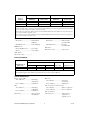
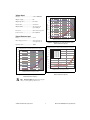
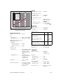
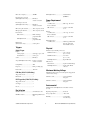
NI 6711/6713/DAQCard-6715 Specifications This document lists the specifications for the NI 6711/6713 and NI DAQCard-6715 analog output devices. The following specifications are typical at 25 °C unless otherwise noted. Note With NI-DAQmx, National Instruments has revised its terminal names so they are easier to understand and more consistent among NI hardware and software products. The revised terminal names used in this document are usually similar to the names they replace. For a complete list of Traditional NI-DAQ (Legacy) terminal names and their NI-DAQmx equivalents, refer to the Terminal Name Equivalents section of Chapter 2, I/O Connector, of the Analog Output Series User Manual. Analog Output Output Characteristics Number of channels NI 6711....................................... 4 voltage outputs NI 6713/DAQCard-6715 ............ 8 voltage outputs Resolution ....................................... 12 bits, 1 in 4,096 Max update rate Max Update Rate (NI 6711/6713) Max Update Rate (NI DAQCard-6715) Number of Channels Using Local FIFO (kS/s)* Using Host PC Memory (kS/s)† Using Local FIFO (kS/s) Using Host PC Memory (kS/s)‡ 1 1,000 1,000 1,000 833 2 1,000 1,000 850 417 3 1,000 1,000 750 282 4 1,000 1,000 650 211 5 1,000 1,000 600 169 6 952 1,000 550 141 Max Update Rate (NI DAQCard-6715) Max Update Rate (NI 6711/6713) Number of Channels Using Local FIFO (kS/s)* Using Host PC Memory (kS/s)† Using Local FIFO (kS/s) Using Host PC Memory (kS/s)‡ 7 833 869 510 121 8 740 769 480 105 * These numbers apply to continuous waveform generation, which allows for the time it takes to reset the FIFO to the beginning when cycling through it. This additional time, about 200 ns, is not incurred when using host PC memory for waveform generation. Max update rate in FIFO mode does not change regardless of the number of devices in the system. † These results were measured using a PCI-6711/6713 device with a 90 MHz Pentium machine. These numbers may change when using more devices or when other CPU or bus activity occurs. ‡ These results were measured using a DAQCard-6715 with a 266 MHz Pentium II machine. These numbers may change when using more devices or when other CPU or bus activity occurs. Type of DAC Data transfers NI 6711/6713 ..............................Double-buffered, multiplying NI 6711/6713.............................. DMA, interrupts, programmed I/O NI DAQCard-6715 .....................Serial, multiplying NI DAQCard-6715 ..................... Interrupts, programmed I/O FIFO buffer size DMA modes (NI 6711/6713 only) ....................... Scatter-gather NI 6711/DAQCard-6715 ............8,192 samples NI 6713 .......................................16,384 samples DMA channels (NI 6711/6713 only) ........................3 Accuracy Information Absolute Accuracy % of Reading Nominal Range at Full Scale (V) 24 Hours 90 Days 1 Year Offset (mV) Temp Drift (%/°C) ±10 0.0177% 0.0197% 0.0219% ±5.933 0.0005% Absolute accuracy = (% of Reading × Voltage) + Offset + (Temp Drift × Voltage) Note: Temp drift applies only if ambient is greater than ±10 °C of previous external calibration. Transfer Characteristics Relative accuracy (INL) Offset error After calibration ..........................±0.3 LSB typ, ±0.5 LSB max After calibration ......................... ±1.0 mV typ, ±5.9 mV max Before calibration .......................±4.0 LSB max Before calibration ....................... ±200 mV max DNL Gain error (relative to internal reference) After calibration ..........................±0.3 LSB typ, ±1.0 LSB max After calibration ......................... ±0.01% of output max Before calibration ....................... ±0.5% of output max Before calibration .......................±3.0 LSB max Gain error (relative to external reference) .......................... +0.0 to +0.67% of output max, not adjustable at >4 V Monotonicity ...................................12 bits guaranteed after calibration NI 6711/6713/DAQCard-6715 Specifications 2 ni.com Voltage Output Ranges............................................. ±10 V, ±EXT REF Scaling Attenuation versus External Reference Frequency 1.6 Output coupling .............................. DC DAC Code All 1.4 Output impedance ........................... 0.1 Ω max 1.2 Output Voltage Current drive ................................... ±5 mA max Output stability ............................... Any passive load, up to 1,500 pF Protection ........................................ Short-circuit to ground Power-on state................................. 0 V (±200 mV) External Reference Input DAC Code 0xBFD 1.0 0.8 DAC Code 0x7FE 0.6 0.4 DAC Code 0x3FF 0.2 DAC Code 0x199 Range .............................................. ±11 V 1 Overvoltage protection ................... ±25 V powered on, ±15 V powered off 1.6 DAC F.S. THD DAC 0.875 THD DAC 0.75 THD DAC 0.625 THD DAC 0.500 THD DAC 0.375 THD DAC 0.250 THD DAC 0.125 THD –10 DAC Code All 1s –20 1.2 –30 DAC Code 0xBFD THD in dB Output Voltage 1000 AO External Reference THD versus External Reference Frequency 0 Scaling Attenuation versus External Reference Frequency 1.0 0.8 10 100 AO External Reference Frequency in kHz Figure 2. NI DAQCard-6715 Scaling Attenuation versus External Reference Frequency Input impedance.............................. 10 kΩ 1.4 DAC Code 0x000 0.0 DAC Code 0x7FE –40 –50 –60 0.6 0.4 DAC Code 0x3FF 0.2 DAC Code 0x199 –70 –80 –90 DAC Code 0x000 0.0 1 10 100 AO External Reference Frequency in kHz 1000 1 10 100 AO External Reference Frequency in kHz 1000 Figure 3. NI 6711/6713 AO External Reference THD versus External Reference Frequency Figure 1. NI 6711/6713 Scaling Attenuation versus External Reference Frequency Note (NI 6711/6713 Only) External reference input is always a 1.414 V peak-to-peak sine wave. © National Instruments Corporation 3 NI 6711/6713/DAQCard-6715 Specifications Stability Offset temperature coefficient ........ ±50 μV/°C AO External Reference THD versus External Reference Frequency 0 –10 –20 THD in dB –30 –40 Gain temperature coefficient DAC F.S. THD DAC 0.875 THD DAC 0.750 THD DAC 0.625 THD DAC 0.500 THD DAC 0.375 THD DAC 0.250 THD DAC 0.125 THD Internal reference........................ ±25 ppm/°C External reference....................... ±25 ppm/°C Onboard calibration reference Level........................................... 5.000 V (±2.5 mV) (actual value stored in EEPROM) –50 –60 Temperature coefficient ............. ±5.0 ppm/°C max –70 Long-term stability ..................... ±15 ppm/ 1,000 h –80 –90 0.1 1 10 AO External Reference Frequency in kHz Digital I/O 100 Number of channels ........................ 8 input/output Compatibility .................................. TTL/CMOS Figure 4. NI DAQCard-6715 AO External Reference THD versus External Reference Frequency Digital logic levels Dynamic Characteristics Level Slew rate ..........................................20 V/μs Noise NI 6711/6713 ..............................200 Vrms, DC to 1 MHz NI DAQCard-6715 .....................400 μVrms, DC to 1 MHz Glitch energy (at mid-scale transition, NI DAQCard-6715 only) Magnitude Reglitching enabled................±4 mV 0V 0.8 V Input high voltage 2.0 V 5.0 V Input low current (Vin = 0 V) — –320 μA Input high current (Vin = 5 V) — 10 μA Output low voltage (IOL = 24 mA) — 0.4 V 4.35 V — Power-on state................................. Input (high-impedance) Duration ......................................1.5 μs Data transfers .................................. Programmed I/O Channel crosstalk NI 6711/6713 ..............................–70 dB with SH68-68-EP cable (generating a 10 V, 10 point sinusoidal at 100 kHz on the reference channel) Timing I/O NI DAQCard-6715 .....................–60 dB (generating a 10 V, 10 point sinusoidal at 100 kHz on the reference channel) Resolution Number of channels ........................ 2 up/down counter/timers, 1 frequency scaler Counter/timers ............................ 24 bits Frequency scaler......................... 4 bits Compatibility .................................. TTL/CMOS Settling time ....................................3.0 μs to ±0.5 LSB accuracy Base clocks available Counter/timers ............................ 20 MHz, 100 kHz Total harmonic distortion ................–80 dB typ (generating a 10 V, 1,000 point, 750 Hz sine wave, summing 9 harmonics) NI 6711/6713/DAQCard-6715 Specifications Max Input low voltage Output high voltage (IOH = –13 mA) Reglitching disabled ...............±20 mV Min Frequency scaler......................... 10 MHz, 100 kHz Base clock accuracy........................ ±0.01% over operating temperature 4 ni.com NI DAQCard-6715 ..........................16-bit PC Card (PCMCIA) Max source frequency..................... 20 MHz External source selections (NI DAQCard-6715 only)............... PFI <0..9>, software-selectable Power Requirement NI 6711 External gate selections (NI DAQCard-6715 only)............... PFI <0..9>, software-selectable +5 VDC (±5%) ...........................0.80 A typ, 1.0 A max Power available at I/O connector ..............................+4.65 to +5.25 VDC at 1 A Min source pulse duration............... 10 ns, edge-detect mode Min gate pulse duration .................. 10 ns, edge-detect mode NI 6713 +5 VDC (±5%) ...........................1.25 A typ, 1.5 A max Data transfers Power available at I/O connector ..............................+4.65 to +5.25 VDC at 1 A NI 6711/6713.............................. DMA, interrupts, programmed I/O NI DAQCard-6715 ..................... Interrupts, programmed I/O NI DAQCard-6715 +5 VDC (±5%) ...........................160 mA typ, 250 mA max plus any current used from the I/O connector DMA modes (NI 6711/6713 only) ....................... Scatter-gather Triggers Physical Digital Trigger Dimensions (not including connectors) Purpose NI PCI-6711/6713.......................17.5 × 10.7 cm (6.87 × 4.2 in.) Analog output ............................. Start trigger, gate, clock NI PXI-6711/6713 ......................16 × 10 cm (6.3 × 3.9 in.) Counter/timers ............................ Source, gate Source ............................................. PFI <0..9> NI DAQCard-6715 .....................Type II PC Card Slope (NI DAQCard-6715 only)..... Positive or negative; software-selectable I/O connector NI 6711/6713 ..............................68-pin male SCSI-II type Compatibility .................................. TTL NI DAQCard-6715 .....................68-pin female Honda connector Response ......................................... Rising or falling edge Pulse width...................................... 10 ns min Maximum Working Voltage RTSI Bus (PCI-6711/6713 Only) Maximum working voltage refers to the signal voltage plus the common-mode voltage. Trigger lines <0..6> ........................ 7 Channel-to-earth..............................±11 V, Installation Category I RTSI clock ...................................... 1 PXI Trigger Bus (PXI-6711/6713 Only) Channel-to-channel .........................±22 V, Installation Category I Trigger lines <0..5> ........................ 6 Star trigger ...................................... 1 Environmental Clock ............................................... 1 The NI 6711/6713/DAQCard-6715 is intended for indoor use only. Bus Interface Operating temperature.....................0 to 50 °C NI PCI-6711/6713........................... 5 V PCI master, slave Storage temperature.........................–20 to 70 °C NI PXI-6711/6713 .......................... PXI/CompactPCI master, slave © National Instruments Corporation Humidity..........................................5 to 90% RH, noncondensing 5 NI 6711/6713/DAQCard-6715 Specifications Note Refer to the Declaration of Conformity (DoC) for this product for any additional regulatory compliance information. To obtain the DoC for this product, visit ni.com/certification, search by model number or product line, and click the appropriate link in the Certification column. Maximum altitude ...........................2,000 meters Pollution Degree..............................2 Note Clean the device with a soft, non-metallic brush. Make sure that the device is completely dry and free from contaminants before returning it to service. Environmental Management National Instruments is committed to designing and manufacturing products in an environmentally responsible manner. NI recognizes that eliminating certain hazardous substances from our products is beneficial not only to the environment but also to NI customers. Safety This product is designed to meet the requirements of the following standards of safety for electrical equipment for measurement, control, and laboratory use: • IEC 61010-1, EN 61010-1 • UL 61010-1, CSA 61010-1 For additional environmental information, refer to the NI and the Environment Web page at ni.com/environment. This page contains the environmental regulations and directives with which NI complies, as well as other environmental information not included in this document. Note For UL and other safety certifications, refer to the product label, or visit ni.com/ certification, search by model number or product line, and click the appropriate link in the Certification column. Waste Electrical and Electronic Equipment (WEEE) EU Customers At the end of their life cycle, all products must be sent to a WEEE recycling center. For more information about WEEE recycling centers and National Instruments WEEE initiatives, visit ni.com/environment/weee.htm. Electromagnetic Compatibility This product is designed to meet the requirements of the following standards of EMC for electrical equipment for measurement, control, and laboratory use: • EN 61326 EMC requirements; Minimum Immunity • EN 55011 Emissions; Group 1, Class A • CE, C-Tick, ICES, and FCC Part 15 Emissions; Class A ⬉ᄤֵᙃѻક∵ᶧࠊㅵ⧚ࡲ⊩ ˄Ё RoHS˅ Ёᅶ᠋ National Instruments ヺড়Ё⬉ᄤֵ ᙃѻકЁ䰤ࠊՓ⫼ᶤѯ᳝ᆇ⠽䋼ᣛҸ (RoHS)DŽ݇Ѣ National Instruments Ё RoHS ড়㾘ᗻֵᙃˈ 䇋ⱏᔩ ni.com/environment/rohs_chinaDŽ (For information about China RoHS compliance, go to ni.com/environment/rohs_china.) Note For EMC compliance, operate this device with shielded cabling. CE Compliance This product meets the essential requirements of applicable European Directives, as amended for CE marking, as follows: • 2006/95/EC; Low-Voltage Directive (safety) • 2004/108/EC; Electromagnetic Compatibility Directive (EMC) NI 6711/6713/DAQCard-6715 Specifications 6 ni.com Device Pinouts AO GND NC AO GND AO GND NC AO GND NC AO GND AO GND AO 3 AO GND AO GND AO 0 AO 1 AO EXT REF P0.4 D GND P0.1 P0.6 D GND +5 V D GND D GND PFI 0 PFI 1 D GND +5 V D GND PFI 5/AO SAMP CLK PFI 6/AO START TRIG D GND PFI 9/CTR 0 GATE CTR 0 OUT FREQ OUT 34 33 32 31 30 29 28 27 26 25 24 23 68 67 66 65 64 63 62 61 60 59 58 57 22 21 20 19 18 17 16 15 14 13 12 11 10 9 8 7 6 5 56 55 54 53 52 51 50 49 48 47 46 45 44 43 42 41 40 39 4 3 2 1 38 37 36 35 NC AO GND AO GND NC AO GND AO GND NC AO GND NC AO GND AO GND AO 2 AO GND AO GND AO GND D GND P0.0 P0.5 D GND P0.2 P0.7 P0.3 NC EXT STROBE D GND PFI 2 PFI 3/CTR 1 SOURCE PFI 4/CTR 1 GATE CTR 1 OUT D GND PFI 7 PFI 8/CTR 0 SOURCE D GND D GND NC = No Connect Figure 5. NI 6711 68-Pin AO I/O Connector Pin Assignments © National Instruments Corporation 7 NI 6711/6713/DAQCard-6715 Specifications AO GND NC AO GND AO GND AO 6 AO GND AO 5 AO GND AO GND AO 3 AO GND AO GND AO 0 AO 1 AO EXT REF P0.4 D GND P0.1 P0.6 D GND +5 V D GND D GND PFI 0 PFI 1 D GND +5 V D GND PFI 5/AO SAMP CLK PFI 6/AO START TRIG D GND PFI 9/CTR 0 GATE CTR 0 OUT FREQ OUT 34 33 32 31 30 29 28 27 26 25 24 23 68 67 66 65 64 63 62 61 60 59 58 57 22 21 20 19 18 17 16 15 14 13 12 11 10 9 8 7 6 5 4 3 2 1 56 55 54 53 52 51 50 49 48 47 46 45 44 43 42 41 40 39 38 37 36 35 NC AO GND AO GND AO 7 AO GND AO GND NC AO GND AO 4 AO GND AO GND AO 2 AO GND AO GND AO GND D GND P0.0 P0.5 D GND P0.2 P0.7 P0.3 NC EXT STROBE D GND PFI 2 PFI 3/CTR 1 SOURCE PFI 4/CTR 1 GATE CTR 1 OUT D GND PFI 7 PFI 8/CTR 0 SOURCE D GND D GND NC = No Connect Figure 6. NI 6713/DAQCard-6715 68-Pin AO I/O Connector Pin Assignments National Instruments, NI, ni.com, and LabVIEW are trademarks of National Instruments Corporation. Refer to the Terms of Use section on ni.com/legal for more information about National Instruments trademarks. Other product and company names mentioned herein are trademarks or trade names of their respective companies. For patents covering National Instruments products, refer to the appropriate location: Help»Patents in your software, the patents.txt file on your CD, or ni.com/patents. © 2004–2007 National Instruments Corporation. All rights reserved. 371011C-01 Aug07