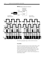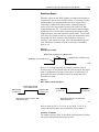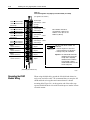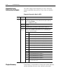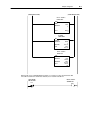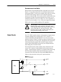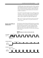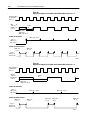
1
AllenBradley
Very HighSpeed
Counter Module
(Cat. No. 1771VHSC Series B)
User
Manual
Important User Information
Because of the variety of uses for the products described in this
publication, those responsible for the application and use of this control
equipment must satisfy themselves that all necessary steps have been taken
to assure that each application and use meets all performance and safety
requirements, including any applicable laws, regulations, codes and
standards.
The illustrations, charts, sample programs and layout examples shown in
this guide are intended solely for example. Since there are many variables
and requirements associated with any particular installation, Allen-Bradley
does not assume responsibility or liability (to include intellectual property
liability) for actual use based upon the examples shown in this publication.
Allen-Bradley publication SGI–1.1, “Safety Guidelines For The
Application, Installation and Maintenance of Solid State Control”
(available from your local Allen-Bradley office) describes some important
differences between solid-state equipment and electromechanical devices
which should be taken into consideration when applying products such as
those described in this publication.
Reproduction of the contents of this copyrighted publication, in whole or
in part, without written permission of Allen–Bradley Company, Inc. is
prohibited.
Throughout this manual we make notes to alert you to possible injury to
people or damage to equipment under specific circumstances.
ATTENTION: Identifies information about practices or
circumstances that can lead to personal injury or death, property
damage or economic loss.
Attention helps you:
Identify a hazard.
Avoid the hazard.
Recognize the consequences.
Important: Identifies information that is especially important for
successful application and understanding of the product.
Important: We recommend you frequently backup your application
programs on appropriate storage medium to avoid possible data loss.
Summary of Changes
Summary of Changes
Summary of Changes
This release of the publication contains new and updated information
from the last release.
New Information
This release includes information on the Series B version of the
1771-VHSC module. This includes a new Appendix E on the
differences between period/rate and continuous/rate modes of
operation. This information was not included in the previous version
of this publication.
Updated Information
This release includes updated information in Appendix C,
“application Considerations,” and revised Specifications in
Appendix A.
Change Bars
To help you find new and updated information in this publication, we
have included change bars as shown to the right of this paragraph.
Table of Contents
Summary of Changes . . . . . . . . . . . . . . . . . . . . . . . .
SOC-1
Summary of Changes . . . . . . . . . . . . . . . . . . . . . . . . . . . . .
New Information . . . . . . . . . . . . . . . . . . . . . . . . . . . . . . . . .
Updated Information . . . . . . . . . . . . . . . . . . . . . . . . . . . . . .
Change Bars . . . . . . . . . . . . . . . . . . . . . . . . . . . . . . . . . . .
SOC-1
SOC-1
SOC-1
SOC-1
Using This Manual . . . . . . . . . . . . . . . . . . . . . . . . . . . . . . .
P-1
Purpose of This Manual . . . . . . . . . . . . . . . . . . . . . . . . . . . . . . .
Audience . . . . . . . . . . . . . . . . . . . . . . . . . . . . . . . . . . . . . . . . . .
Vocabulary . . . . . . . . . . . . . . . . . . . . . . . . . . . . . . . . . . . . . . . .
Manual Organization . . . . . . . . . . . . . . . . . . . . . . . . . . . . . . . . .
Related Products . . . . . . . . . . . . . . . . . . . . . . . . . . . . . . . . . . . .
Product Compatibility . . . . . . . . . . . . . . . . . . . . . . . . . . . . . . . . .
Related Publications . . . . . . . . . . . . . . . . . . . . . . . . . . . . . . . . . .
P-1
P-1
P-1
P-1
P-2
P-2
P-2
Overview of the Very High Speed Counter Module . . . . . . .
1-1
Chapter Objectives . . . . . . . . . . . . . . . . . . . . . . . . . . . . . . . . . . .
Module Description . . . . . . . . . . . . . . . . . . . . . . . . . . . . . . . . . .
Features of the Module . . . . . . . . . . . . . . . . . . . . . . . . . . . . . . . .
Operation in Encoder or Counter Mode . . . . . . . . . . . . . . . . . . . .
Counter Mode . . . . . . . . . . . . . . . . . . . . . . . . . . . . . . . . . . . . . .
Encoder Mode . . . . . . . . . . . . . . . . . . . . . . . . . . . . . . . . . . . . . .
Preset Value . . . . . . . . . . . . . . . . . . . . . . . . . . . . . . . . . . . . . . .
Rollover Value . . . . . . . . . . . . . . . . . . . . . . . . . . . . . . . . . . . . . .
Software Reset . . . . . . . . . . . . . . . . . . . . . . . . . . . . . . . . . . . . .
Gate/Reset Input . . . . . . . . . . . . . . . . . . . . . . . . . . . . . . . . . . . .
Operation in Period/Rate Mode . . . . . . . . . . . . . . . . . . . . . . . . . .
Continuous/Rate Mode . . . . . . . . . . . . . . . . . . . . . . . . . . . . . . . .
Operation in Rate Measurement Mode . . . . . . . . . . . . . . . . . . . . .
Outputs . . . . . . . . . . . . . . . . . . . . . . . . . . . . . . . . . . . . . . . . . . .
Enabling and Forcing Outputs . . . . . . . . . . . . . . . . . . . . . . . . . . .
Assigning Outputs to Counters . . . . . . . . . . . . . . . . . . . . . . . . . .
Operation of Outputs . . . . . . . . . . . . . . . . . . . . . . . . . . . . . . . . .
Handshaking . . . . . . . . . . . . . . . . . . . . . . . . . . . . . . . . . . . . . . .
Default Configuration . . . . . . . . . . . . . . . . . . . . . . . . . . . . . . . . .
How the Module Communicates with a Programmable Controller . .
Chapter Summary . . . . . . . . . . . . . . . . . . . . . . . . . . . . . . . . . . .
1-1
1-1
1-1
1-2
1-3
1-4
1-6
1-7
1-7
1-7
1-9
1-12
1-12
1-14
1-14
1-14
1-15
1-16
1-16
1-17
1-18
ii
Table of Contents
Installing the Very HighSpeed Counter Module . . . . . . . . .
2-1
Chapter Objectives . . . . . . . . . . . . . . . . . . . . . . . . . . . . . . . . . . .
European Union Directive Compliance . . . . . . . . . . . . . . . . . . . . .
EMC Directive . . . . . . . . . . . . . . . . . . . . . . . . . . . . . . . . . . . .
Low Voltage Directive . . . . . . . . . . . . . . . . . . . . . . . . . . . . . . .
Electrostatic Damage . . . . . . . . . . . . . . . . . . . . . . . . . . . . . . . . .
Power Requirements . . . . . . . . . . . . . . . . . . . . . . . . . . . . . . . . .
Module Location in the I/O Chassis . . . . . . . . . . . . . . . . . . . . . . .
Module Keying . . . . . . . . . . . . . . . . . . . . . . . . . . . . . . . . . . . . . .
Setting the Configuration Jumpers . . . . . . . . . . . . . . . . . . . . . . . .
Connecting Wiring . . . . . . . . . . . . . . . . . . . . . . . . . . . . . . . . . . .
Grounding the VHSC Module Wiring . . . . . . . . . . . . . . . . . . . . . .
Installing the Module . . . . . . . . . . . . . . . . . . . . . . . . . . . . . . . . .
Interpreting the Indicator Lights . . . . . . . . . . . . . . . . . . . . . . . . . .
Chapter Summary . . . . . . . . . . . . . . . . . . . . . . . . . . . . . . . . . . .
2-1
2-1
2-1
2-1
2-2
2-2
2-2
2-3
2-4
2-5
2-6
2-7
2-8
2-8
Module Programming . . . . . . . . . . . . . . . . . . . . . . . . . . . .
3-1
Chapter Objectives . . . . . . . . . . . . . . . . . . . . . . . . . . . . . . . . . . .
Block Transfer Programming . . . . . . . . . . . . . . . . . . . . . . . . . . . .
PLC2 Program Example . . . . . . . . . . . . . . . . . . . . . . . . . . . . . .
PLC3 Program Example . . . . . . . . . . . . . . . . . . . . . . . . . . . . . .
PLC5 Program Example . . . . . . . . . . . . . . . . . . . . . . . . . . . . . .
PLC5/250 Program Example . . . . . . . . . . . . . . . . . . . . . . . . . . .
Chapter Summary . . . . . . . . . . . . . . . . . . . . . . . . . . . . . . . . . . .
3-1
3-1
3-2
3-3
3-4
3-5
3-5
Configuring Your Module . . . . . . . . . . . . . . . . . . . . . . . . . .
4-1
Chapter Objectives . . . . . . . . . . . . . . . . . . . . . . . . . . . . . . . . . . .
Configuring the VHSC Module . . . . . . . . . . . . . . . . . . . . . . . . . . .
Configuration Block for a Block Transfer Write . . . . . . . . . . . . . . .
Bit/Word Descriptions . . . . . . . . . . . . . . . . . . . . . . . . . . . . . . . . .
Chapter Summary . . . . . . . . . . . . . . . . . . . . . . . . . . . . . . . . . . .
4-1
4-1
4-2
4-3
4-7
Module Status and Input Data . . . . . . . . . . . . . . . . . . . . . .
5-1
Chapter Objectives . . . . . . . . . . . . . . . . . . . . . . . . . . . . . . . . . . .
Reading Data from the Module . . . . . . . . . . . . . . . . . . . . . . . . . .
Block Transfer Read for the 1771VHSC Module . . . . . . . . . . . . . .
Bit/Word Description for Block Transfer Read . . . . . . . . . . . . . . . .
Chapter Summary . . . . . . . . . . . . . . . . . . . . . . . . . . . . . . . . . . .
5-1
5-1
5-1
5-3
5-4
Table of Contents
iii
Troubleshooting . . . . . . . . . . . . . . . . . . . . . . . . . . . . . . . .
6-1
Chapter Objectives . . . . . . . . . . . . . . . . . . . . . . . . . . . . . . . . . . .
Using the Indicators for Troubleshooting . . . . . . . . . . . . . . . . . . . .
Troubleshooting Chart . . . . . . . . . . . . . . . . . . . . . . . . . . . . . .
Diagnostic Codes Returned by the Module . . . . . . . . . . . . . . . . . .
Diagnostics Reported in Word 1 of BTR . . . . . . . . . . . . . . . . . .
Chapter Summary . . . . . . . . . . . . . . . . . . . . . . . . . . . . . . . . . . .
6-1
6-1
6-1
6-2
6-2
6-2
Specifications . . . . . . . . . . . . . . . . . . . . . . . . . . . . . . . . . .
A-1
Sample Programs . . . . . . . . . . . . . . . . . . . . . . . . . . . . . . .
B-1
Sample Program for PLC-2 Family Processors . . . . . . . . . . . . . .
Sample Program for PLC-5 Family Processors . . . . . . . . . . . . . .
Addditional Sample Program for PLC-5 Family Processors . . . . . .
B-1
B-2
B-4
Application Considerations . . . . . . . . . . . . . . . . . . . . . . . .
C-1
Appendix Objectives . . . . . . . . . . . . . . . . . . . . . . . . . . . . . . . . . .
Types of Input Devices . . . . . . . . . . . . . . . . . . . . . . . . . . . . . . . .
Examples for Selecting Input Devices . . . . . . . . . . . . . . . . . . . . .
Circuit Overview . . . . . . . . . . . . . . . . . . . . . . . . . . . . . . . . . . . . .
Detailed Circuit Analysis . . . . . . . . . . . . . . . . . . . . . . . . . . . . . . .
5V Differential Line Driver Example . . . . . . . . . . . . . . . . . . . . . . .
+12 to +24V SingleEnded Driver . . . . . . . . . . . . . . . . . . . . . . . .
Open Collector . . . . . . . . . . . . . . . . . . . . . . . . . . . . . . . . . . . . . .
Supply Voltage verses Jumper Settings . . . . . . . . . . . . . . . . . .
Electromechanical Limit Switch . . . . . . . . . . . . . . . . . . . . . . . . . .
Output Circuits . . . . . . . . . . . . . . . . . . . . . . . . . . . . . . . . . . . . . .
Application Considerations . . . . . . . . . . . . . . . . . . . . . . . . . . . . .
Input Cable Length . . . . . . . . . . . . . . . . . . . . . . . . . . . . . . . . . . .
Totempole Output Devices . . . . . . . . . . . . . . . . . . . . . . . . . . . . .
Cable Impedance . . . . . . . . . . . . . . . . . . . . . . . . . . . . . . . . . . . .
Cable Capacitance . . . . . . . . . . . . . . . . . . . . . . . . . . . . . . . . . . .
Cable Length and Frequency . . . . . . . . . . . . . . . . . . . . . . . . . . .
C-1
C-1
C-1
C-2
C-3
C-4
C-5
C-6
C-6
C-7
C-7
C-8
C-8
C-8
C-9
C-9
C-9
Questions and Answers . . . . . . . . . . . . . . . . . . . . . . . . . . .
D-1
General . . . . . . . . . . . . . . . . . . . . . . . . . . . . . . . . . . . . . . . . . . .
Questions and Answers . . . . . . . . . . . . . . . . . . . . . . . . . . . . . . .
D-1
D-1
Period/Rate and Continuous/Rate Examples . . . . . . . . . . .
E-1
General . . . . . . . . . . . . . . . . . . . . . . . . . . . . . . . . . . . . . . . . . . .
Changes made in Revision B . . . . . . . . . . . . . . . . . . . . . . . . . . .
Operation of Outputs in Period/rate Mode
(1771VHSC Revision B Modules) . . . . . . . . . . . . . . . . . . . . .
Operation of Outputs in Continuous/Rate Mode . . . . . . . . . . . . . . .
E-1
E-2
E-3
E-4
Preface
Using This Manual
Purpose of This Manual
Audience
This manual shows you how to use the Very High Speed Counter
module with an Allen-Bradley programmable controller. It helps you
install, program, and troubleshoot your module.
You must be able to program and operate an Allen-Bradley
programmable controller (PLC) to make efficient use of this module.
In particular, you must know how to program your PLC for block
transfer-type instructions.
We assume that you know how to do this in this manual. If you do
not, refer to the appropriate programming and operations manual for
the associated programmable controller before you attempt to use
this module.
Vocabulary
In this manual, we refer to:
• the Very High Speed Counter module as the “module,” the
“1771-VHSC” or the “VHSC module.”
• the programmable controller as the “controller,” or the “PLC.”
Manual Organization
This manual is divided into six chapters. The following chart shows
each chapter with its corresponding title and a brief description of
the topics covered in that chapter.
Chapter
Title
Topics Covered
1
Overview of the Very High Speed Counter Module
Explanation of modes, outputs, default
configuration and how the module communicates
with the processor.
2
Installing the Very High Speed Counter Module
How to install, key, connect wiring, ground and an
explanation of the indicators on the module.
3
Module Programming
Block transfer programming and programming
examples.
4
Configuring Your Module
Configuration and description of bit/words for block
transfer write instructions.
5
Module Status and Input Data
Reading data from the module and bit/word
description of the block transfer read.
6
Troubleshooting
Using the indicators for troubleshooting and
diagnostic codes.
P–2
Using This Manual
Chapter
Title
Topics Covered
Appendices
A
Specifications
Specifications for the VHSC module.
B
Sample Programs
Sample programs for various PLC programs.
C
Application Considerations
Selection of input devices and circuit descriptions.
D
Questions and Answers
Helpful answers to the most asked questions.
E
Period/Rate and Continuous/Rate Examples
Examples of the differences of these 2 modes
Related Products
You can install your input module in any system that uses
Allen-Bradley programmable controllers with block transfer
capability and the 1771 I/O structure.
Contact your nearest Allen-Bradley office for more information
about your programmable controllers.
Product Compatibility
This module can be used with any 1771 I/O chassis. Communication
between the module and the processor is bidirectional. The PLC
sends module information using block transfer write instructions and
the 1771 I/O backplane. The PLC receives module status information
through block transfer read instruction and places it in the data table.
I/O image table use is an important factor in module placement and
addressing selection. The module’s data table use is listed in the
following table.
Table P.A
Compatibility and Use of Data Table
Catalog
Number
Input
Image
Bits
Use of Data Table
Output Read
Image Block
Bits
Words
Write
Block
Words
Compatibility
1/2 slot
Addressing
1slot
2slot
Chassis
Series
1771VHSC Rev. A
8
8
18 max
64 max
Yes
See note
See note
A and B
1771VHSC Rev. B
8
8
26 max
64 max
Yes
See note
See note
A and B
A = Compatible with 1771A1, A2, A4 chassis.
B = Compatible with 1771A1B, A2B, A3B, A4B chassis.
Yes = Compatible without restriction
NOTE: Restricted to complementary module placement (refer to chapter 2)
Related Publications
For a list of publications with information on Allen-Bradley
programmable controller products, consult our publication index
SD499.
Chapter
1
Overview of the Very High
Speed Counter Module
Chapter Objectives
This chapter gives you information on:
• features of the VHSC module
• how the module communicates with programmable controllers.
• how the module operates
Module Description
The VHSC module performs high speed counting for industrial
applications. The module is an intelligent block transfer I/O module
that interfaces signals with any Allen-Bradley programmable
controller that has block transfer capability. Block transfer
programming moves module status data from the module’s memory
to a designated area in the processor data table. It also moves
configuration words from the processor data table to the module
memory.
The VHSC module is a single-slot module that does not require an
external power supply. (Note: The outputs do require a power
supply.) After scanning the inputs and updating the outputs, the input
data is converted to a specified data type in a digital format to be
transferred to the processor’s data table on request. Command and
configuration data is sent from the programmable controller data
table to the module with a BTW instruction.
Features of the Module
The VHSC module counts pulses from encoders (such as
Allen-Bradley Bulletin 845H, K, F, P, E and L), pulse generators or
mechanical limit switches, proximity switches, etc. and returns either
a count or frequency in binary or BCD format.
The module’s features include:
• 4 input channels configurable for encoder mode, counter mode,
•
•
•
•
•
•
period/rate mode and continuous/rate mode
8 outputs, isolated in groups of 2
outputs are current-sourcing at 5 to 24V dc (2A maximum per
output)
single-ended or differential inputs
2-phase encoder inputs up to a frequency of 250KHz
single-phase counter inputs up to a frequency of 1MHz
input voltage range of 5 to 24V dc
1–2
Overview of the Very High Speed Counter Module
• returns in status either count or frequency in binary or BCD
format
• input counts as high as 999,999
• up to 500KHz in period/rate or rate measurement frequency
modes
• outputs can be tied to any counter
• each output has a user-selectable on-off value
• outputs can be tied back to an input for cascading
• automatic default configuration
• each counter has a user-selectable preset and rollover value
• period/rate w/periodic outputs and period/rate w/dynamic outputs
can be used for totalization
The 1771-VHSC module operates in the following modes:
•
•
•
•
•
•
counter mode
encoder X1 mode
encoder X4 mode
period/rate mode
rate measurement frequency mode
continuous/rate mode
The operation of the module in these modes is described below.
Operation in Encoder or
Counter Mode
The operation of encoder and counter modes is virtually identical.
The only difference between the two modes is in the type of
feedback used.
Use the counter mode if you need the module to read incoming
pulses from a maximum of four encoders (single-ended or
differential), counters, pulse generators, mechanical limit switches,
etc. and return them to the programmable controller as a binary or
BCD number (0-999,999). In counter mode, the module accepts only
one channel feedback.
Use the encoder modes if you need the module to read incoming
quadrature pulses and return them to the programmable controller as
a binary or BCD number (0-999,999). In these modes, the module
accepts two-phase quadrature feedback and counts up or down
depending upon the condition of the phase B input for each counter.
The operation of the module in the encoder/counter modes is as
follows:
Overview of the Very High Speed Counter Module
1–3
• counter mode - channel B is tied high or low. Channel A input is
used for pulse. The count is unidirectional with the direction
determined by
channel B.
• encoder X1 - This is a bidirectional count mode; counting up or
down, using quadrature input signals.
• encoder X4 - This is a bidirectional count mode, using quadrature
input signals, with 4 times the resolution of X1.
Each of the counters in encoder/counter mode has values associated
with it. These are:
•
•
•
•
preset value
rollover value
gate/reset input
output
Counter Mode
The counter mode allows the module to read incoming pulses and
return them to the programmable controller processor as a binary or
BCD number (0-999,999).
In the counter mode, direction (up counting or down counting) is
determined by the phase B input, which can be a random signal. If
Phase B is high, the counter will count down. If phase B is low or
floating, (that is, not connected), the counter counts up.
If Phase B is:
Counter will count (direction):
High
Down
Low or floating (not connected)
Up
The module reads incoming pulses from a maximum of 4 encoders
(single-ended or differential), counters, pulse generators, mechanical
limit switches, and so forth and returns a count to the programmable
controller processor in a binary or BCD number (0-999,999).
1–4
Overview of the Very High Speed Counter Module
The counter mode accepts only one phase feedback. This
relationship is shown in 1.1.
Figure 1.1
Block Diagram of Counter Mode
From Encoder/Pulse Generator
Phase A
Terminal
Phase B
Terminal
(direction sense)
1771VHSC
Gate/Reset
Terminal
10677I
Encoder Mode
The encoder mode allows the module to read incoming pulses and
return them to the programmable controller processor as a binary or
BCD number (0-999,999).
In this mode, the module will accept two phase quadrature feedback.
The module senses the relationship between the 2 phases and counts
up or down accordingly.
Encoder X1 mode uses channel A for the pulse input. With B low
(floating), the count direction is up; when B is high, the count
direction is down.
Encoder X4 mode is identical to X1, except it uses quadrature
signals on channel A and channel B, and counts on the leading and
trailing edges of
A and B.
Overview of the Very High Speed Counter Module
1–5
Figure 1.2
Block Diagram of Encoder Mode
From Encoder/Pulse Generator
Phase A
Terminal
1771VHSC
Phase B
Terminal
(direction sense)
Gate/Reset
Terminal
10678I
Direction of Count
The module can count either up or down, depending upon the
condition of the B input for each counter. In encoder applications,
the counter will increment on the leading edge of Phase A, while
phase B determines the direction of the count.
You also have the option of X1 and X4 multiplying of the input
pulses. 1.3 shows the relationships between phases A and B for
forward and reverse directions in encoder applications.
1–6
Overview of the Very High Speed Counter Module
Figure 1.3
Phase Relationship for Forward or Reverse Directions
Very High Speed
Counter Module
Phase A
Encoder
Input A
Encoder
Input B
Phase B
Forward Rotation
CCW Encoder Rotation
Reverse Rotation
CW Encoder Rotation
Phase A
T
4µsec
min
Phase B
90
1µsec
Typical
90
1
X1
Multiplying
1
2
3
4
5
2
1
0
3
2
6
7
8
9
10
11
12
12
11
10
9
8
7
6
5
4
3
2
1
X4
Multiplying
10679I
The following paragraphs apply to both encoders and counters.
Preset Value
Each of the 4 counters has one preset value associated with it. In the
encoder or counter modes, the preset value represents a reference
point (or count) from which the module begins counting. The
module can count either up or down from the preset value. Preset
values are loaded into the count registers through the preset count
bits. (Refer to word 1, bits 8-11 of the block transfer write
initialization block in chapter 5.) Preset values can range from 0 to
999,999 binary or BCD.
0
Overview of the Very High Speed Counter Module
1–7
Rollover Value
Each of the 4 counters has one rollover value associated with it.
When the rollover value is reached by the encoder/counter, it resets
to 0 and begins counting again. The rollover values range from 0 to
999,999 binary or BCD (0 represents 1,000,000). The rollover value
is circular (for example: if you program 360, the count will be from
358, 359, 0, 1 etc. in a positive direction and from 1, 0, 359, 358 etc.
in a negative direction).
Software Reset
The counters can also be reset by the Reset Count bits found in Word
1, bits 0-3 of the block transfer write. When one of these bits is set
to 1, the associated counter is reset to zero and begins counting. The
module can also be reset with the gate/reset as explained below.
Refer to chapter 4 for further details.
Gate/Reset Input
There is one gate/reset input for each of the 4 counters. The
gate/reset input, when active, will function in one of the 4 store count
modes outlined below.
Scaling Input Count at the Gate/Reset Terminal
You can scale the incoming count at the gate/reset terminal. Scaling
allows the incoming pulses at gate/reset to be divided by a number in
the range of 1, 2, 4, 8, 16, 32, 64 and 128. Refer to words 21 to 24 in
the BTW file (chapter 4).
Store Count
The store count feature allows the module to store the current count
value of any (or all) of the four counters. The store count feature is
triggered by the state of the gate/reset terminal on the module. The
stored count of each counter is placed in a separate word in the
Block Transfer Read file (words 11-18 respectively). The stored
count value will remain in the block transfer read file until a new
trigger pulse is received at the Gate/Reset terminal. When a new
trigger pulse is received, the old count value will be overwritten by
the new value.
The store count feature is selected by words 3 and 4 of the block
transfer write initialization file. Refer to chapter 4 for further details.
1–8
Overview of the Very High Speed Counter Module
In mode 1, store/continue (1.4), the leading edge of a pulse input on
the gate/reset terminal will cause the current value in the counter to
be read and stored. The counter will continue counting. The stored
count will be available in the block transfer read file. The stored
count information will remain in the block transfer read file until it is
overwritten by new data.
Figure 1.4
Store/Continue
Read, Store Count
and continue counting.
10680I
In mode 2, store/wait/resume (1.5), the gate/reset terminal provides
the capability to inhibit counting when the gate/reset input is high.
Counting resumes when the input goes low. Mode 2 does not reset
the counter, although it does store the count value.
Figure 1.5
Store/Wait/Resume
Stop counting
Store Count
Resume counting
10681I
In mode 3, store-reset/wait/start (1.6), the rising edge of the pulse
on the gate/reset terminal causes the counter to stop counting, store
the current count value in the block transfer read file and reset the
count to zero. The counter does not count while the input pulse on
the gate/reset terminal remains high. Counting resumes from zero on
the falling edge of the pulse at the gate/reset terminal.
Figure 1.6
StoreReset/Wait/Start
Counter has stopped counting
Stop count, store
and reset to zero
Start counting
from zero
10682I
In mode 4, store-reset/start (1.7), on the rising edge of a pulse
input at the gate/reset terminal will cause the counter to store the
accumulated count value and will reset the counter to zero. The
counter continues counting, and the stored count is available in the
block transfer read file.
Overview of the Very High Speed Counter Module
1–9
Figure 1.7
StoreReset/Start
Rising Edge
Store Count,
reset to zero,
start counting.
Falling Edge
Store Count,
reset to zero,
start counting.
10683I
Figures 1.4 through 1.7 show the store count feature operating on the
rising edge of the gate/reset pulse. The user has the option of
selecting these same features using the falling edge of the gate/reset
pulse. This selection is made through the gate invert bit as explained
in chapter 4.
The gate invert bit is active in the store count, continuous/rate
and period/rate modes.
The stored count values are saved in words 11 through 18 of the
block transfer read file (chapter 4).
Operation in
Period/Rate Mode
Use the period/rate mode to determine the frequency of input pulses
by counting the number of internal 4MHz clock pulses over a
user-specified number of input signal pulses. At the end of the
specified number of pulses, the module returns the frequency and the
number of internal 4MHz pulses.
A channel configured for period/rate mode acts as a period rate
counter. An internal 4 MHz clock is used as a frequency reference.
This clock is gated by the incoming pulse train at the gate/reset
input. The results of this gating action are the number of pulses or a
frequency. The number of sampled gated 4MHz pulses are returned
in BTR words 3 thru 10, and the frequency in words 11 thru 18.
Select the period/rate mode by setting the appropriate bits in words
3 and 4 of the BTW initialization file (chapter 4). The store count
features are inactive in period/rate mode.
1771-VHSC revision B and later modules count the total number of
pulses occurring at the gate/reset pin. This function is
frequency-limited. This total count is returned when you request
words 19 through 26 in your BTR. You can reset this count by
resetting the reset bit (bits 0-4 in BTW
word 1). Rollover and preset are inactive. Refer to appendix E for
additional information.
1.8 shows a diagram of the module used in the period/rate mode.
1–10
Overview of the Very High Speed Counter Module
Figure 1.8
Period/Rate Mode
A Not used
From user's encoder/pulse generator
1771VHSC
B Not used
Gate/Reset Terminal
From internal 4MHz clock
scaler
Incoming pulse train
at gate/reset terminal
Sampled pulses
4MHz internal clock
10684I
In 1.8, the incoming pulse train from the gate/reset terminal is used
to sample pulses from the 4 MHz internal clock. As the frequency of
the incoming pulse train at the gate/reset terminal increases, the
number of sampled pulses from the 4 Mhz clock decreases. This
relationship is shown in Table 1.A. Since accuracy is related to the
number of pulses received over the sample period, the accuracy will
decrease with increasing input frequencies at the Gate/Reset
terminal. To some extent, the decrease in accuracy can be lessened
by scaling the input frequency through the use of a scaler. A scaler
value of 1 will only return an accurate input frequency if incoming
pulses have a 50% duty cycle. If frequency exceeds 500KHz, the
number 999,999 is returned.
Overview of the Very High Speed Counter Module
1–11
Table 1.A
Relationship Between Sampled Pulses and Input Frequency
Input Frequency at Gate/Reset
Terminal in Hz
(words 1118 in BTR)
Sampled Pulses for 1/2 Cycle
of Gate/Reset Pulse
(words 310 in BTR)
2
1 meg
5
400K
10
200K
20
100K
50
40K
100
20K
200
10K
500
4K
1KHz
2K
2KHz
1K
5KHz
400
10KHz
200
20KHz
100
50KHz
40
100KHz
20
200KHz
10
Operation of scaler
In period/rate mode, the scaler lets the incoming pulse train at the
gate/reset pin be divided by a user defined number. Acceptable
values for the scaler are 1, 2, 4, 8, 16, 32, 64 and 128. There is one
scaler value for each counter. The default value for each scaler is 1.
Note: A 0 is equivalent to 1.
!
ATTENTION: Sample period times scaler must be
less than 0.25 seconds or the counter will overflow
without providing an overflow indication.
Connection to Counter Inputs
The only input to the module in the period/rate mode is made to the
gate/reset terminal. The counter inputs (channel A and B) are not
used in the period/rate mode.
1–12
Overview of the Very High Speed Counter Module
Continuous/Rate Mode
The continuous/rate mode is similar to the period/rate mode
previously described except the outputs in this mode are dynamic
outputs. Use this mode to determine the frequency of input pulses by
counting the number of internal 4MHz clock pulses over a
user-specified number of input signal pulses. Each output is turned
on as soon as the turn-on count is reached, and turned off as soon as
the turn-off count is reached. As the internal 4MHz clock is counted,
the outputs dynamically track the 4MHz count. This allows you to
turn an output on a certain number of 4MHz counts after the
gate/reset pin goes active, and turn it off a certain number of 4MHz
counts later.
1771-VHSC revision B and later modules count the total number of
pulses occurring at the gate/reset pin. This function is
frequency-limited. This total count is returned when you request
words 19 through 26 in your BTR. You can reset this count by
resetting the reset bit (bits 0-4 in BTW
word 1). Rollover and preset are inactive. Refer to appendix E for
additional information.
Figure 1.9
Period/Rate and Continuous/Rate Output Operation with
Scaler of 1
Incoming pulse train
at gate/reset terminal
Sampled pulses
4MHz internal clock
Period/rate
Continuous/rate
Operation in Rate
Measurement Mode
Output on/off presets
active only on scaler
number pulse.
Output on/off presets
active during entire
pulse.
10684I
Use the rate measurement mode to count incoming pulses for a
user-specified time interval. At the end of the interval, the module
returns a value representing the sampled number of pulses and a
value indicating the incoming frequency. When the count and
frequency are updated, any associated outputs are checked against
their associated presets.
Overview of the Very High Speed Counter Module
1–13
The value representing the sampled number of pulses is returned in
BTR words 3 thru 10, and the value indicating the incoming
frequency is returned in words 11-18. The total count equals the
number of pulses received during the sample period. The operation
of rate measurement mode is shown below in 1.10.
Figure 1.10
Operation of the Rate Measurement Mode
From user's encoder/pulse generator
Channel A
1771VHSC
Module
Channel B
(not used)
Gate/Reset terminal
(not used)
From user's encoder/pulse generator
Userselectable sample time
10685I
Example:
In 1.10, three counts have been accumulated during the user-selected
time period. If you had selected 50 milliseconds as the sample
period, the frequency returned to the programmable controller
processor in words 11-12 would be:
Frequency = Counts/Sample period = 3 counts/50 milliseconds = 60
Hz
You would read 60 Hz as the frequency in the Block Transfer Read
file (words 11 and 12). Words 3 and 4 would contain the value 3.
Since the default configuration for the VHSC module is the Counter
mode, the user must select the rate measurement mode through the
block transfer write initialization file. This is done by setting the
appropriate bits in words 3 and 4 of the block transfer write
initialization file (chapter 4). If frequency exceeds 500KHz, the
number 999,999 is returned.
1–14
Overview of the Very High Speed Counter Module
Sample Period
You can set the sample period used in the frequency calculation in
the rate measurement mode. Allowable values are 10 milliseconds to
2 seconds in 10 millisecond increments. The default value is 1
second. (Note: A 0 in the BTW initialization word is equivalent to
the default value of 1 second.)
The sample period is set in words 21 through 24 of the BTW
initialization file (chapter 4).
Connection to Counter Inputs
The only user connections used in the rate measurement mode are to
phase A of the module. The gate/reset and channel B terminals are
not used in this mode.
Outputs
The VHSC module has 8 outputs, isolated in groups of 2. Each of
the outputs is capable of sourcing current and will operate between 5
and 24 volts dc. You must connect an external power supply to each
of the outputs. The outputs can source 2 amps dc. The outputs are
hardware-driven and will turn on in less than 10µsec when the
appropriate count value has been reached.
Enabling and Forcing Outputs
Outputs may be forced on or off independent of count or frequency
value. To force the outputs, they must first be enabled. Enabling the
outputs is done through a data table word 2, bits 0-7 in the BTW
initialization file (chapter 4). Once the outputs have been enabled,
they may be forced on by setting bits 8-15 in word 2 of the BTW
initialization file. The outputs can be forced off by setting the enable
bit to 0.
Assigning Outputs to Counters
By setting bits in the block transfer write initialization file, you can
assign the outputs on the module to any of the various counters. You
can assign as many as 8 outputs to a given counter. However, an
output may be assigned only once to a counter--it is not possible to
use the same output with 2 different counters. Refer to words 25, 30,
35, 40, 45, 50, 55, 60 of the BTW initialization file in chapter 4.
Overview of the Very High Speed Counter Module
1–15
Operation of Outputs
When the outputs for the VHSC module are enabled and assigned to
a counter they operate in an ON-OFF fashion. For example, assume
that the module were programmed to turn ON an output when a
count value of 2000 was reached. Further, assume that the user
desired to have the output remain energized for a period of 3000
counts and then turn OFF. The end result would be that the outputs
would turn ON at count of 2000, would remain energized for 3000
additional counts, and would turn OFF at 5000 counts. The ON and
OFF values are circular around zero. In the rate measurement mode,
the On and Off values associated with each output represent a
frequency value instead of a count value. The maximum frequency
value which may be entered in an On or Off value is 500,000Hz.
Refer to 1.11.
Figure 1.11
OnOff Operation of Output
Output remains energized for 3000 additional counts
Output turns off at count value of 5000
Output turns on at count value of 2000
10686I
Refer to 1.12. Using output 0 as an example, when the value in
words 26 and 27 is less than the value in words 28 and 29, the output
turns on at 2000 and off at 5000. If the value in words 26 and 27 is
greater than the value in words 28 and 29, the output turns off at
2000 and on at 5000.
Figure 1.12
Effect of Values in Words 26 through 29
Output remains energized
for 3000 additional counts.
Output turns ON
at count of 2000.
When values in words 2627 are less than
values in words 2829.
Output turns OFF
at count of 5000.
Output turns OFF
at count of 2000.
Output turns ON
at count of 5000.
When values in words 2627 are greater than
values in words 2829.
10687I
Refer to words 26-29, 31-34, 36-39, 41-44, 46-49, 51-54, 56-59,
61-64 of the block transfer write initialization file in chapter 5.
Isolation of Outputs
The module provides 1500V ac forced rms isolation between each of
the counters and the backplane of the I/O rack.
1–16
Overview of the Very High Speed Counter Module
Tying Outputs to Counters
You can jumper any of the outputs to any of the counter inputs on the
module field wiring arm. In this way, it is possible to use the outputs
to reset a counter or to cascade counters. If using the outputs this
way, make certain that the input voltage jumpers are set to interface
with the appropriate output voltage.
Handshaking
A pair of handshaking bits are provided for each counter. These bits
are called New Data (ND) bits in the BTR instruction, and New Data
Acknowledge (NDA) bits in the BTW instruction. They indicate
when a stored data value has been most recently updated. These bits
are provided for count/accumulate applications, but can be used
whenever the stored data is updated at a rate slower than the block
transfer time.
The New Data bit (BTR status word 1, bits 4-7 for counters 0-3
respectively) can be used by the ladder program to indicate that a
store register (BTR words 11-18) has been updated by one of the
following events:
An active gate transition in any of the store count modes
The end of the gate sample period in either the period/rate or
continuous/rate modes
The end of the programmed sample period in rate
measurement mode
The ND bit is reset in the ladder program by a 0 to 1 transition of the
corresponding NDA bit, and then performing a BTW. A BTW length
of 1 word can be use for this handshaking procedure.
Note: A BTW length of 1 has no effect on the preset or reset bits in
BTW word 1, and does not qualify as a configuration BTW. (For
example, if the BTW valid bit is set, it will remain set after the BTW
with a length of 1 is sent.)
Default Configuration
A default configuration is built into the module. The default
configuration is automatically selected on power-up if the user has
not configured the module through a Block Transfer Write
Initialization file. The module can be placed in the default
configuration by writing a block transfer write initialization file with
all zeroes to the module.
Overview of the Very High Speed Counter Module
1–17
The default mode for the VHSC module is the counter mode for all 4
of the counters. In the default configuration, the module will
continuously return counts (0-999,999 binary) to the programmable
controller processor. The presets and rollovers associated with each
of the 4 counters will not be active, nor will any of the outputs be
active.
How the Module
Communicates with a
Programmable Controller
The processor transfers data to and from the module using block
transfer write (BTW) and block transfer read (BTR) instructions in
your ladder diagram program. These instructions let the processor
obtain input values and status from the module, and let you establish
the module’s mode of operation (1.13).
Figure 1.13
How the Module Communicates with a Programmable
Controller
3
6
1
BTW
5
User Program
BTR
2
Data Table
4
VHSC Module
1771VHSC
PC Processor
(PLC5/15 Shown)
12933I
1. The processor transfers your configuration data and commands to
the module using a BTW instruction.
2. External devices generate input signals that are transmitted to the
module.
3. The module converts these signals into binary or BCD format,
and stores these values and controls their output until the
processor requests their transfer.
4. When instructed by your ladder program, the processor performs
a BTR of the values and stores them in a data table.
5. The processor and module determine that the transfer was made
without error, and that input values are within a specified range.
1–18
Overview of the Very High Speed Counter Module
6. Your ladder program can use/or move the data (if valid) before it
is written over by the transfer of new data in a subsequent
transfer.
Chapter Summary
In this chapter you learned how your module operates, and how your
module communicates with the programmable controller.
Chapter
2
Installing the Very HighSpeed
Counter Module
Chapter Objectives
This chapter gives you information on:
•
•
•
•
•
calculating the chassis power requirement
keying a chassis slot for your module
setting the voltage and filter jumpers
wiring the input module’s field wiring arm
installing the input module
Before installing your module in the I/O chassis you must:
Before You Install Your
Module
Action required:
Refer to:
Calculate the power requirements of all modules in each chassis.
Power Requirements
Determine where to place the module in the I/O chassis.
Module Location in the I/O Chassis
Key the backplane connector in the I/O chassis.
Module Keying
Make connections to the wiring arm.
Connecting Wiring and Grounding
European Union Directive
Compliance
If this product is installed within the European Union or EEA
regions and has the CE mark, the following regulations apply.
EMC Directive
This apparatus is tested to meet Council Directive 89/336/EEC
Electromagnetic Compatibility (EMC) using a technical construction
file and the following standards, in whole or in part:
• EN 50081-2
EMC – Generic Emission Standard, Part 2 –
Industrial Environment
• EN 50082-2 EMC – Generic Immunity Standard, Part 2 –
Industrial Environment
The product described in this manual is intended for use in an
industrial environment.
Low Voltage Directive
This apparatus is also designed to meet Council Directive 73/23/EEC
Low Voltage, by applying the safety requirements of EN 61131–2
Programmable Controllers, Part 2 – Equipment Requirements and
Tests.
For specific information that the above norm requires, see the
appropriate sections in this manual, as well as the following
Allen-Bradley publications:
2–2
Installing the Very High-Speed Counter Module
• Industrial Automation Wiring and Grounding Guidelines,
publication 1770-4.1
• Guidelines for Handling Lithium Batteries, publication AG-5.4
• Automation Systems Catalog, publication B111
Electrostatic Damage
Electrostatic discharge can damage semiconductor devices inside this
module if you touch backplane connector pins. Guard against
electrostatic damage by observing the following warning:
!
ATTENTION: Electrostatic discharge can degrade
performance or cause permanent damage. Handle the
module as stated below.
• Wear an approved wrist strap grounding device when handling
the module.
• Touch a grounded object to rid yourself of electrostatic charge
before handling the module.
• Handle the module from the front, away from the backplane
connector. Do not touch backplane connector pins.
• Keep the module in its static-shield bag when not in use, or
during shipment.
Power Requirements
Your module receives its power through the 1771 I/O chassis
backplane from the chassis power supply. The maximum current
drawn by the module from this supply is 650mA (3.25 Watts).
Add this value to the requirements of all other modules in the I/O
chassis to prevent overloading the chassis backplane and/or
backplane power supply.
Module Location in the
I/O Chassis
Place your module in any slot of the I/O chassis except for the
extreme left slot. This slot is reserved for processors or adapter
modules.
When using:
You can:
2slot addressing
place your module in any module group with any 8bit or block
transfer module.
1slot addressing
place your module in any module group with any 8bit, 16bit or block
transfer module.
1/2slot addressing,
no restrictions on module location.
After determining the module’s location in the I/O chassis, connect
the wiring arm to the pivot bar at the module’s location.
Installing the Very High-Speed Counter Module
Module Keying
2–3
Use the plastic keying bands, shipped with each I/O chassis, for
keying the I/O slot to accept only this type of module.
The module is slotted in two places on the rear edge of the circuit
board. The position of the keying bands on the backplane connector
must correspond to these slots to allow insertion of the module. You
can key any connector in an I/O chassis to receive these modules
except for the leftmost connector reserved for adapter or processor
modules. Place keying bands between the following numbers
labeled on the backplane connector (Figure 2.1):
• Between 24 and 26
• Between 28 and 30
You can change the position of these bands if subsequent system
design and rewiring makes insertion of a different type of module
necessary. Use needlenose pliers to insert or remove keying bands.
Figure 2.1
Keying Positions
Keying Bands
2
4
6
8
10
12
14
16
18
20
22
24
26
28
30
32
34
36
Upper Connector
14288
2–4
Installing the Very High-Speed Counter Module
Setting the Configuration
Jumpers
The VHSC module has user-selectable jumpers for each input
channel. These jumpers consist of one each:
• filter or high speed operation jumper
• +5V or +12-24V operation jumper
Each counter has a total of 6 jumpers associated with it:
•
•
•
•
•
•
Channel A filter/high speed jumper
Channel A voltage jumper
Channel B filter/high speed jumper
Channel B voltage jumper
Gate/reset filter/high speed jumper
Gate/reset voltage jumper
These jumpers can be set independent of each other. You can select
the filter action and voltage for each channel and for the gate/reset
input independently.
The high speed operation is the preferred mode of operation for the
1771-VHSC module. Use this mode when the inputs are driven by
devices such as encoders or line drivers.
Use the filter mode on the inputs when a mechanical switch is
providing the input. The filter provides de-bouncing for the
mechanical switch. The frequency of counting must be less than
100Hz when the filter mode is selected.
Use these jumpers to match the operation of the module with the
input supplied. Settings are shown in Figure 2.2.
To set the jumpers, proceed as follows:
1. Remove the four screws securing the side cover to the module
and remove the covers.
2. Using your fingers, reposition the jumpers associated with each
input channel according to your requirements. Refer to
Figure 2.2.
Installing the Very High-Speed Counter Module
2–5
Figure 2.2
Setting the Configuration Jumpers
Filter Jumper
Position
Voltage Jumper
Position
Down
Down
Down
Up
Up
Down
Up
Up
Description of Operation
1224V High Speed (factory default setting)
5V High Speed
1224V with low speed filter
5V with low speed filter
*
FILTER
HI SPEED
5V
1224V
A0
B0
G0
10688I
*In the filter position, the module will not see frequencies above 100Hz.
3. Reposition the cover and secure with the 4 screws removed in
step 1.
Connecting Wiring
Connect your I/O devices to the 40-terminal field wiring arm (cat.
no. 1771-WN) shipped with the module (Figure 2.3). Attach the
field wiring arm to the pivot bar at the bottom of the I/O chassis.
The field wiring arm pivots upward and connects with the module so
you can install or remove the module without disconnecting the
wires.
2–6
Installing the Very High-Speed Counter Module
Figure 2.3
Connection Diagram for Very High Speed Counter Module (1771VHSC)
(See applicable codes and laws.)
Channel A/Channel A Return
2
Channel B/Channel B Return
4
Gate Not input
6
Gate Not input
8
Channel B/Channel B Return
10
Channel A/Channel A Return
12
Channel A/Channel A Return
14
Channel B/Channel B Return
16
Gate Not Input
Gate Not Input
18
Channel B/Channel B Return
22
20
Channel A/Channel A Return
24
Output 0
Customer Common 01
26
Output 2
Customer Common 23
30
Output 4
Customer Common 45
34
Output 6
38
Customer Common 67
40
28
32
36
Channel A Input
Channel B Input Counter 0
Gate Input
Gate Input
Channel B Input Counter 1
Channel A Input
Channel A Input
Channel B Input Counter 2
Gate Input
Gate Input
Channel B Input Counter 3
Channel A Input
Customer VCC 01
Output 1
Customer VCC 23
Output 3
Customer VCC 45
Output 5
Customer VCC 67
Output 7
(Actual wiring runs in this direction.)
Grounding the VHSC
Module Wiring
Note: Terminals on the left are
even numbered (2 thru 40), and
terminals on the right are odd
numbered (1 thru 39).
The sensor cable must be shielded. The
shield must:
• extend the length of the cable, but be
connected only at the 1771 I/O chassis
• extend up to the point of termination
Important: The shield should extend to the
termination point, exposing just
enough cable to adequately
terminate the inner conductors.
Use heat shrink or another
suitable insulation where the wire
exits the cable jacket.
10689I
When using shielded cable, ground the foil shield and drain wire
only at one end of the cable. We recommend that you wrap the foil
shield and drain wire together and connect them to a chassis
mounting bolt (Figure 2.4). At the opposite end of the cable, tape
exposed shield and drain wire with electrical tape to insulate it from
electrical contact.
Installing the Very High-Speed Counter Module
2–7
Figure 2.4
Cable Grounding
Ground Shield at
I/O
chassis
mounting bolt
Shield and drain
twisted into single
strand
Field Wiring Arm
17798
Refer to Wiring and Grounding Guidelines, publication 1770-4.1 for
additional information.
Installing the Module
When installing your module in an I/O chassis:
1. First, turn off power to the I/O chassis:
!
ATTENTION: Remove power from the 1771 I/O
chassis backplane and wiring arm before removing or
installing an I/O module.
Failure to remove power from the backplane could
cause injury or equipment damage due to possible
unexpected operation.
Failure to remove power from the backplane or wiring
arm could cause module damage, degradation of
performance, or injury.
2. Place the module in the plastic tracks on the top and bottom of the
slot that guides the module into position.
3. Do not force the module into its backplane connector. Apply firm
even pressure on the module to seat it properly.
2–8
Installing the Very High-Speed Counter Module
4. Snap the chassis latch over the top of the module to secure it.
5. Connect the wiring arm to the module.
Interpreting the Indicator
Lights
The front panel of the input module contains 12 input indicators, 8
output indicators, an active indicator and a fault indicator
(Figure 2.5). At power-up, the active and fault indicators are on. An
initial module self-check occurs. If there is no fault, the red indicator
turns off. If a fault is found initially or occurs later, the fault indicator
lights and the active indicator is forced off.
When an input LED (A, B) is on, it indicates that the input is high.
When the output LED is on, it indicates that the module has
commanded the output to be on. When a gate/reset indicator (G) is
on, its input is high. Since that signal can be inverted, it does not
indicate whether the signal on that terminal is necessarily logically
true.
Possible module fault causes and corrective action are discussed in
the chapter titled “Troubleshooting.”
Figure 2.5
Diagnostic Indicators
ACTIVE
INPUTS
A0 A1 A2 A3
B0 B1 B2 B3
G0 G1 G2 G3
OUTPUTS
00 02 04 06
01 03 05 07
FAULT
Active Indicator
Input Indicators
Output Indicators
Fault Indicator
10690I
Chapter Summary
In this chapter you learned how to install your input module in an
existing programmable controller system and how to wire to the field
wiring arm.
Chapter
3
Module Programming
Chapter Objectives
In this chapter we describe:
block transfer programming
sample programs in the PLC-2, PLC-3 and PLC-5 processors
Block Transfer
Programming
Your module communicates with the processor through bidirectional
block transfers. This is the sequential operation of both read and
write block transfer instructions.
The following example programs accomplish this handshaking
routine. These are minimum programs; all rungs and conditioning
must be included in your application program. You can disable
BTRs, or add interlocks to prevent writes if desired. Do not eliminate
any storage bits or interlocks included in the sample programs. If
interlocks are removed, the program may not work properly.
Optionally, the block transfer write (BTW) instruction is initiated
when the module is first powered up, and subsequently only when
the programmer wants to write a new configuration to the module.
At all other times the module is basically in a repetitive block
transfer read (BTR) mode.
Your module will work with a default configuration of all zeroes
entered in the configuration block. See the configuration default
section to understand what this configuration looks like. Also, refer
to Appendix B for example configuration blocks and instruction
addresses to get started.
The following example programs illustrate the minimum
programming required for communication to take place.
3–2
Module Programming
PLC2 Program Example
Figure 3.1 below shows a sample PLC-2 program.
Figure 3.1
PLC2 Family Sample Program Structure
The VHSC module is located in rack 1, module group 0, slot 0. The data address 030 is among the first available timer/counters used for block transfer.
The default block length of 0 results in a 18 word block transfer read. The module status data is returned to the processor starting at address 301.
If a block length other than 0 is specified for the BTR or BTW the BTR and BTW cannot be enabled during the scan.
1
VHSC BTR
Done Bit
110
07
VHSC BTW
Enable Bit
010
06
VHSC BTR Data Address
BTR
BLOCK TRANSFER READ
DATA ADDRESS:
030
MODULE ADDRESS:
100
BLOCK LENGTH:
00
FILE:
301-400
010
EN
07
110
DN
07
The VHSC module is located in rack 1, module group 0, slot 0. The data address 031 is among the first available timer/counters used for block transfer.
The default block length of 0 results in a 64 word block transfer write. The module configuration data is stored starting at address 201. The preconditions
could also include the configuration bit (word 1, bit 0) to limit the block transfer write.
2
VHSC BTW
Done Bit
110
06
VHSC BTR
Enable Bit
010
07
BTW
BLOCK TRANSFER WRITE
DATA ADDRESS:
031
MODULE ADDRESS:
100
BLOCK LENGTH:
00
FILE:
201-300
010
EN
06
110
DN
06
This rung is used to place a zero between the first available timer counters used for all block transfers and those used throughout the rest of
the program.
032
032
3
G
PUT
0
0
This rung uses a BTR done bit to trigger a move of the count data stored at 301 to a buffered location at 331. The program should access all data
from the buffered file (count 0 MSD would be located in word 333 and the LSD in word 334.)
VHSC BTR
Done Bit
4
110
07
FFM
FILE TO FILE MOVE
COUNTER ADDR:
033
POSITION:
1
FILE LENGTH:
18
FILE A:
301-322
FILE R:
331-352
RATE PER SCAN:
18
033
EN
17
033
DN
15
Module Programming
PLC3 Program Example
3–3
Block transfer instructions with the PLC-3 processor use one binary
file in a data table section for module location and other related data.
This is the block transfer control file. The block transfer data file
stores data that you want transferred to the module (when
programming a block transfer write) or from the module (when
programming a block transfer read). The address of the block
transfer data files are stored in the block transfer control file.
The industrial terminal prompts you to create a control file when a
block transfer instruction is being programmed. The same block
transfer control file is used for both the read and write
instructions for your module. A different block transfer control file
is required for every module.
A sample program is shown in Figure 3.2 below.
Figure 3.2
PLC3 Family Sample Program Structure
The VHSC module is located in rack 1, module group 0, slot 0. The control file is a 10 word file, shared by the BTR and BTW, starting at B12:0.
The data obtained by the processor from the VHSC is placed in memory starting at location N13:101, and with the default length of 0 is 18 words
long. The MSD of counter 0 is stored in N13:103 and the LSD of counter 0 is stored in N13:104.
VHSC BTR/BTW
Control Block
VHSC BTR
Done Bit
B12:0
15
VHSC BTR
Error Bit
BTR
BLOCK XFER READ
1
RACK:
0
GROUP:
0
MODULE:
CNTL:
B12:0
N13:101
DATA:
LENGTH:
0
EN
DN
ER
VHSC BTR
Error Bit
B12:0
B12:0
U
13
13
The VHSC module is located in rack 1, module group 0, slot 0. The control file is a 10 word file, shared by the BTR and BTW, starting at B12:0.
The data sent by the processor to the VHSC is placed in memory starting at location N13:1, and with the default length of 0 is 64 words long. If the
default mode of VHSC operation is desired (rollover at 999,999 outputs disabled), this rung can be optional. The module configured bit can also
be used as a precondition to increase BTR throughput.
VHSC BTR/BTW
VHSC BTW
Control Block
Done Bit
BTW
B12:0
BLOCK XFER WRITE
EN
1
RACK:
0
GROUP:
5
DN
0
,MODULE:
CNTL:
B12:0
ER
N13:1
DATA:
LENGTH:
0
VHSC BTW
VHSC BTW
Error Bit
Error Bit
B12:0
3
B12:0
U
3
3–4
Module Programming
PLC5 Program Example
Block transfer instructions with the PLC-5 processor use one binary
file in a data table section for module location and other related data.
This is the block transfer control file. The block transfer data file
stores data that you want transferred to the module (when
programming a block transfer write) or from the module (when
programming a block transfer read). The address of the block
transfer data files are stored in the block transfer control file.
The industrial terminal prompts you to create a control file when a
block transfer instruction is being programmed. A different block
transfer control file is used for the read and write instructions
for your module.
Figure 3.3
PLC5 Family Sample Program Structure
The VHSC module is located in rack 0, module group 0, slot 0. The BTR control file starts at N21:0 and is 5 words long. The data obtained by the
processor from the VHSC is placed in memory starting at location N22:101, and with the default length of 0 is 18 words long. The MSD of counter
0 is stored in N22:103 and the LSD of counter 0 is stored in N22:104.
VHSC BTR
Control File
VHSC
BTW
VHSC BTR
Enable Bit
BTR
Enable Bit
BLOCK XFER READ
EN
N21:5
N21:0
0
RACK:
1
0
GROUP:
DN
0
MODULE:
15
15
N21:0
CONTROL:
ER
DATA FILE:
N22:101
LENGTH:
0
CONTINUOUS:
N
The VHSC module is located in rack 0, module group 0, slot 0. The BTWcontrol file starts at N21:5 and is a 5 words long.
The data sent by the processor to the VHSC is stored in memory starting at location N22:1, and with the default length of 0 is 64 words long.
2
VHSC BTR
Enable Bit
N21:0
15
VHSC BTW
Enable Bit
N21:5
15
VHSC BTW
Control File
BTW
BLOCK XFER WRITE
0
RACK:
0
GROUP:
0
MODULE:
N21:5
CONTROL:
DATA FILE:
N22:1
LENGTH:
0
CONTINUOUS:
N
EN
DN
ER
Module Programming
PLC5/250 Program
Example
3–5
Block transfer instructions with the PLC-5/250 processor use one
binary file in a data table section for module location and other
related data. This is the block transfer control file. The block transfer
data file stores data that you want transferred to the module (when
programming a block transfer write) or from the module (when
programming a block transfer read). The address of the block
transfer data files are stored in the block transfer control file.
The industrial terminal will automatically select the control file
based on rack, group, and slot, and whether it is a read or write. A
different block transfer control file is used for the read and write
instructions for your module. A different block transfer control file
is required for every module.
Figure 3.4
PLC5/250 Family Sample Program Structure
The VHSC module is located in rack 0, module group 0, slot 0. The data obtained by the processor from the VHSC is placed in memory starting
at location 1BTD0:101, and with the default length of 0 is 18 words long. The MSD of counter 0 is stored in 1BTD0:103 and the LSD of counter 0
is stored in 1BTD0:104.
VHSC BTR
Control File
VHSC
BTW
VHSC BTR
Enable Bit
BTR
Enable Bit
BLOCK XFER READ
EN
BW000:0
BR000:0
0
RACK:
1
0
GROUP:
DN
0
MODULE:
EN
EN
BR000:0
CONTROL BLOCK
ER
DATA FILE:
1BTD0:101
BT LENGTH:
0
CONTINUOUS:
NO
BT TIMEOUT
4
The VHSC module is located in rack 0, module group 0, slot 0. The data sent by the processor to the VHSC is stored in memory starting at location
1BTD0:1, and with the default length of 0 is 64 words long.
2
VHSC BTR
Enable Bit
BR000:0
EN
Chapter Summary
VHSC BTW
Enable Bit
BW000:0
EN
VHSC BTW
Control File
BTW
BLOCK XFER WRITE
0
RACK:
0
GROUP:
0
MODULE:
CONTROL BLOCKBW000:0
DATA FILE:
1BTD0:1
BT LENGTH:
0
CONTINUOUS:
NO
BT TIMEOUT:
4
EN
DN
ER
In this chapter, you learned how to program your programmable
controller and you were given sample programs for each family of
controllers. For additional programs, refer to Appendix B.
Chapter
4
Configuring Your Module
Chapter Objectives
Configuring the VHSC
Module
In this chapter you will read how to configure your module’s
hardware, condition your inputs and enter your data.
You must configure your module to conform to the input device and
specific application that you have chosen. Data is conditioned
through a group of data table words that are transferred to the
module using a block transfer write (BTW) instruction.
You can configure the following features for the 1771-VHSC
module:
•
•
•
•
type of input
data format
preset values
rollover values
Configure your module for its intended operation by means of your
programming terminal and write block transfers.
Note: Programmable controllers that use 6200 software (release 4.2
or higher) programming tools can take advantage of the IOCONFIG
Addendum utility to configure this module. IOCONFIG Addendum
uses menu–based screens for configuration without having to set
individual bits in particular locations. Refer to your 6200 software
literature for details.
Important:
It is strongly recommended that you use IOCONFIG
Addendum to configure this module. The IOCONFIG
Addendum utility greatly simplifies configuration. If
the IOCONFIG Addendum is not available, you must
enter data directly into the data table. Use this chapter
as a reference when performing this task.
During normal operation, the processor transfers from 1 to 64 words
to the module when you program a BTW instruction to the module’s
address.
4–2
Configuring Your Module
Configuration Block for a
Block Transfer Write
The complete configuration block for the block transfer write to the
module is defined in Table 4.A below.
Table 4.A
Configuration Block for the VHSC Module Block Transfer Write
Word
15
1
Format
2
14
13
12
11
10
09
Preset
08
07
06
05
04
03
New Data Acknowledge
Force Outputs
02
Enable Outputs
Gate/
Reset
Counter 1 configuration
Gate/
Reset
Counter 0 configuration
4
Gate/
Reset
Counter 3 configuration
Gate/
Reset
Counter 2 configuration
5
Rollover Counter 0 MSD
6
Rollover Counter 0 LSD
7
Rollover Counter 1 MSD
8
Rollover Counter 1 LSD
9
Rollover Counter 2 MSD
10
Rollover Counter 2 LSD
11
Rollover Counter 3 MSD
12
Rollover Counter 3 LSD
13
Preset Counter 0 MSD
14
Preset Counter 0 LSD
15
Preset Counter 1 MSD
16
Preset Counter 1 LSD
17
Preset Counter 2 MSD
18
Preset Counter 2 LSD
19
Preset Counter 3 MSD
20
Preset Counter 3 LSD
21
Scaler 1, Counter 0
22
Scaler 2, Counter 1
23
Scaler 3, Counter 2
24
Scaler 4, Counter 3
Not used
Tie Output 0 to Counter
26
Output 0 On MSD
27
Output 0 On LSD
28
Output 0 Off MSD
29
Output 0 Off LSD
30
00
Reset
3
25
01
Not used
Tie Output 1 to Counter
31
Output 1 On MSD
32
Output 1 On LSD
33
Output 1 Off MSD
Configuring Your Module
Word
15
14
13
12
11
10
09
34
08
07
06
05
04
03
02
4–3
01
00
Output 1 Off LSD
Words repeat for each additional output: 3539 output 2, 4044 output 3, 4549 output 4, 5054 output 5, 5559 output 6
60
Not used
Tie Output 7 to Counter
61
Output 7 On MSD
62
Output 7 On LSD
63
Output 7 Off MSD
64
Output 7 Off LSD
Bit/Word Descriptions
Bit/word descriptions of BTW file words are presented in Table 4.B.
Enter data into the BTW instruction after entering the instruction into
your ladder diagram program.
Table 4.B
Bit/Word Definitions for the VHSC Module
Word
Word 1
Word 2
Bits
Description
bits 0003
These bits control the reset function. When one of these bits
transitions from 0 to 1, the counter is reset to 0 and begins counting.
The bits correspond to the 4 counters: bit 00 = counter 0; bit 01 =
counter 1; bit 02 = counter 2; bit 03 = counter 3.
bits 0407
New data acknowledge bits. When one of these bits transitions from 0
to 1 the corresponding new data bit in BTR word 1, bits 47 will be
reset. Bit 04 corresponds to counter 0, bit 05 to counter 1, etc.
bits 0811
These bits control the preset function. When one of these bits is set to
1, the preset count value is automatically loaded into the counter and
the counter begins counting. (Note: The preset count values are
loaded into words 13 through 20.) The bits correspond to the counters
as follows: Bit 08 = counter 0; bit 09 = counter 1; bit 10 = counter 2; bit
11 = counter 3.
bits 1214
Not used
bit 15
This bit determines whether BCD or binary format is used.
Bit 15 = 0 Indicates all values in the BTW file and the BTR file will be
in binary. (Diagnostic byte (word 1) is always BCD.)
Bit 15 = 1 Indicates all values in the BTW file and the BTR file will be
in BCD.
bits 0007
Enables outputs. Bit 00 corresponds to output 0, bit 01 to output 1,
etc. Outputs must be enabled before they can be turned ON. Bits
must be set (1) before the output can be turned on.
bits 0815
Output forcing bits. Setting a bit to 1 allows the output to be forced. Bit
08 corresponds to output 0, bit 09 corresponds to output 1, etc.
Outputs must also be enabled.
4–4
Configuring Your Module
Word
Bits
Word 3
bits 0002
Description
Determine rate measurement mode, encoder mode, counter mode or
period/rate mode for COUNTER 0.
Mode
Bit
02
01
00
Counter mode
0
0
0
Encoder X1 mode
0
0
1
Encoder X4 mode
0
1
0
Counter not used
0
1
1
Period/rate mode
1
0
0
Rate Measurement mode
1
0
1
Continuous/rate mode
1
1
0
06
05
04
Store count mode not used for counter 0
0
0
0
Mode 1 (store/continue) used
0
0
1
Mode 2 (store/wait/resume) used
0
1
0
Mode 3 (storereset/wait/start) used
0
1
1
Mode 4 (storereset/start) used
1
0
0
bit 03
Not used
bits 0406
Determine store count mode for COUNTER 0.
Mode
Bit
bit 07
Invert signal bit for gate/reset terminal.
0 = Not inverted
1 = Inverted
bits 0810
Determine rate measurement mode, encoder mode, counter mode or
period/rate mode for COUNTER 1.
Mode
Bit
10
09
08
Counter mode
0
0
0
Encoder X1 mode
0
0
1
Encoder X4 mode
0
1
0
Counter not used
0
1
1
Period/rate mode
1
0
0
Rate Measurement mode
1
0
1
Continuous/rate mode
1
1
0
14
13
12
Store count mode not used for counter 1
0
0
0
Mode 1 (store/continue) used
0
0
1
Mode 2 (store/wait/resume) used
0
1
0
Mode 3 (storereset/wait/start) used
0
1
1
Mode 4 (storereset/start) used
1
0
0
bit 11
Not used
bits 1214
Determine store count mode for COUNTER 1.
Mode
Bit
Configuring Your Module
Word
Word 4
Bits
4–5
Description
bit 15
Invert signal bit for gate/reset terminal.
0 = Not inverted
1 = Inverted
bits 0002
Determine rate measurement mode, encoder mode, counter mode or
period/rate mode for COUNTER 2.
Mode
Bit
02
01
00
Counter mode
0
0
0
Encoder X1 mode
0
0
1
Encoder X4 mode
0
1
0
Counter not used
0
1
1
Period/rate mode
1
0
0
Rate Measurement mode
1
0
1
Continuous/rate mode
1
1
0
06
05
04
Store count mode not used for counter 2
0
0
0
Mode 1 (store/continue) used
0
0
1
Mode 2 (store/wait/resume) used
0
1
0
Mode 3 (storereset/wait/start) used
0
1
1
Mode 4 (storereset/start) used
1
0
0
bit 03
Not used
bits 0406
Determine store count mode for COUNTER 2.
Mode
Bit
bit 07
Invert signal bit for gate/reset terminal.
0 = Not inverted
1 = Inverted
bits 0810
Determine rate measurement mode, encoder mode, counter mode or
period/rate mode for COUNTER 3.
Mode
Bit
10
09
08
Counter mode
0
0
0
Encoder X1 mode
0
0
1
Encoder X4 mode
0
1
0
Counter not used
0
1
1
Period/rate mode
1
0
0
Rate Measurement mode
1
0
1
Continuous/rate mode
1
1
0
14
13
12
Store count mode not used for counter 3
0
0
0
Mode 1 (store/continue) used
0
0
1
Mode 2 (store/wait/resume) used
0
1
0
Mode 3 (storereset/wait/start) used
0
1
1
bit 11
Not used
bits 1214
Determine store count mode for COUNTER 3.
Mode
Bit
4–6
Configuring Your Module
Word
Bits
Description
Mode 4 (storereset/start) used
bit 15
1
0
0
Invert signal bit for gate/reset terminal.
0 = Not inverted
1 = Inverted
Words 5
thru 12
Rollover value. When rollover value is reached, the counter value
becomes 000,000 and counting continues from that point. The range
for both MSD and LSD is 0 to 999.
Word 5
Rollover value. Most significant digit for counter 0.
Word 6
Rollover value. Least significant digit for counter 0.
Word 7
Rollover value. Most significant digit for counter 1.
Word 8
Rollover value. Least significant digit for counter 1.
Word 9
Rollover value. Most significant digit for counter 2.
Word 10
Rollover value. Least significant digit for counter 2.
Word 11
Rollover value. Most significant digit for counter 3.
Word 12
Rollover value. Least significant digit for counter 3.
Words 13
thru 20
Preset values. The preset value is loaded into the respective counter
when its preset bit is set. The preset count value overrides the current
count, and becomes the new count value in the counter. When a
preset value is loaded, the counter begins to count from that value.
Word 13
Preset value. Most significant digit for counter 0.
Word 14
Preset value. Least significant digit for counter 0.
Word 15
Preset value. Most significant digit for counter 1.
Word 16
Preset value. Least significant digit for counter 1.
Word 17
Preset value. Most significant digit for counter 2.
Word 18
Preset value. Least significant digit for counter 2.
Word 19
Preset value. Most significant digit for counter 3.
Word 20
Preset value. Least significant digit for counter 3.
Words 21
thru 24
The ranges of words 21 thru 24 depend on the mode selected in word
3, bits 0002.
In encoder/counter mode or period/rate mode, these are scalar words,
and divide the incoming pulse train at the gate/reset terminal by a
predetermined integer (1, 2, 4, 8, 16, 32, 64 and 128). Default value
is 1.
In rate measurement mode, these are time base values. Range is in
milliseconds from 10ms to 2 seconds in 10ms intervals.
Word 25
bits 0003
Allows you to tie the output to any of the 4 counters. Bits correspond
to the counters: bit 00 for counter 0, bit 01 for counter 1, bit 02 for
counter 2, and bit 03 for counter 3.
bits 0415
Not used.
Word 26
Most significant digit of the ON value of output 0.
Word 27
Least significant digit of the ON value of output 0.
Word 28
Most significant digit of the OFF value of output 0.
Word 29
Least significant digit of the OFF value of output 0.
Words 30
thru 34
These words are a repeat of words 25 through 29 with the exception
of the output number. These words are for output 1.
Configuring Your Module
Word
Chapter Summary
Bits
4–7
Description
Words 35
thru 39
These words are a repeat of words 25 through 29 with the exception
of the output number. These words are for output 2.
Words 40
thru 44
These words are a repeat of words 25 through 29 with the exception
of the output number. These words are for output 3.
Words 45
thru 49
These words are a repeat of words 25 through 29 with the exception
of the output number. These words are for output 4.
Words 50
thru 54
These words are a repeat of words 25 through 29 with the exception
of the output number. These words are for output 5.
Words 55
thru 59
These words are a repeat of words 25 through 29 with the exception
of the output number. These words are for output 6.
Words 60
thru 64
These words are a repeat of words 25 through 29 with the exception
of the output number. These words are for output 7.
In this chapter you learned how to configure your module’s
hardware, condition your inputs and enter your data.
Chapter
5
Module Status and Input Data
Chapter Objectives
In this chapter you will read about:
• reading data from your module
• module read block transfer format
Reading Data from the
Module
Block transfer read (BTR) programming moves status and data from
the input module to the processor’s data table (Table 5.A). The
processor user program initiates the request to transfer data from the
module to the processor.
Block Transfer Read for
the 1771VHSC Module
The module transfers up to 26 words to the processor’s data table
file. The words contain module status and input data from each
channel. When a BTR of length 0 is programmed, the module
returns 18 words.
Important:
Words 19 through 26 are optional, and are accessed
only by programming a BTR length greater than 18
words. Words 19 through 26 are only valid if in
period/rate or continuous/rate modes. In any other
mode words 19 through 26 are zero.
Table 5.A
BTR Word Assignments for the VHSC Module (1771VHSC)
(Octal Bit)
Decimal Bit
17
16
15
14
13
12
11
10
15
14
13
12
11
10
09
08
07
06
05
04
07
06
05
04
02
01
03
02
01
Not Used
00
00
1
Diagnostics (always in BCD)
2
Not used
3
Counter 0 MSD (0999)
4
Counter 0 LSD (0999)
5
Counter 1 MSD (0999)
6
Counter 1 LSD (0999)
7
Counter 2 MSD (0999)
8
Counter 2 LSD (0999)
9
Counter 3 MSD (0999)
10
Counter 3 LSD (0999)
11
Counter 0 Store count values MSD (range 0999) in encoder/counter mode; or frequency
value MSD (range 0500) in rate measurement or period/rate mode
12
Counter 0 Store count values LSD (range 0999)
Gate/Reset input
state
New Data
03
PU*
Status of outputs
5–2
Module Status and Input Data
(Octal Bit)
17
16
15
14
13
12
11
10
07
06
05
04
03
02
01
00
Decimal Bit
15
14
13
12
11
10
09
08
07
06
05
04
03
02
01
00
13
Counter 1 Store count values MSD (range 0999) in encoder/counter mode; or frequency
value MSD (range 0500) in rate measurement or period/rate mode
14
Counter 1 Store count values LSD (range 0999)
15
Counter 2 Store count values MSD (range 0999) in encoder/counter mode; or frequency
value MSD (range 0500) in rate measurement or period/rate mode
16
Counter 2 Store count values LSD (range 0999)
17
Counter 3 Store count values MSD (range 0999) in encoder/counter mode; or frequency
value MSD (range 0500) in rate measurement or period/rate mode
18
Counter 3 Store count values LSD (range 0999)
19
Counter 0 Total counts occurring at gate/reset pin in period/rate or continuous/rate modes
(MSD range = 0999)
20
Counter 0 Total counts occurring at gate/reset pin in period/rate or continuous/rate modes
(LSD range = 0999)
21
Counter 1 Total counts occurring at gate/reset pin in period/rate or continuous/rate modes
(MSD range = 0999)
22
Counter 1 Total counts occurring at gate/reset pin in period/rate or continuous/rate modes
(LSD range = 0999)
23
Counter 2 Total counts occurring at gate/reset pin in period/rate or continuous/rate modes
(MSD range = 0999)
24
Counter 2 Total counts occurring at gate/reset pin in period/rate or continuous/rate modes
(LSD range = 0999)
25
Counter 3 Total counts occurring at gate/reset pin in period/rate or continuous/rate modes
(MSD range = 0999)
26
Counter 3 Total counts occurring at gate/reset pin in period/rate or continuous/rate modes
(LSD range = 0999)
* PU = Power up bit (refer to word/bit description)
Note: Words 19 through 26 are optional and used only in period/rate and continuous/rate modes. They can only be accessed by making
the BTR length between 19 and 26.
Module Status and Input Data
Bit/Word Description for
Block Transfer Read
Table 5.B provides bit/word descriptions for the block transfer read
instruction returned by the 1771-VHSC module to the processor.
Table 5.B
Bit/Word Description for the VHSC Module (1771VHSC)
Word
Word 1
Word 2
5–3
Bit
Definition
Bit 00
Powerup bit indicates whether a successful BTW with valid data has
occurred since powerup, or since last switched from Program to Run
mode.
Bit = 0 A successful BTW has occurred
Bit = 1 A successful BTW has not occurred
Bits 0103
Not used
Bits 0407
New data bits. Indicates that a store register (BTR words 1118) has
been updated. These bits are reset by a 0 to 1 transition of the new
data acknowledge bits in BTW word 1, bits 47. Bit 04 corresponds to
counter 0, bit 05 to counter 1, etc.
Bits 0815
(Bits 1017)
Diagnostic byte. Always in BCD. This byte indicates the number of the
first word in the BTW file that was incorrect. Refer to chapter 7 for
other diagnostic error codes returned by the module.
Bits 0007
Status bits for outputs. Bit 00 corresponds to output 0, bit 01 to
counter 2, etc.
Bit = 0 output OFF
Bit = 1 output ON
Bits 0811
(Bits 1012)
State of gate/reset input. Bit 08 (10) corresponds to counter 0,
bit 09 (11) to counter 1, etc.
Bit = 0 gate input inactive
Bit = 1 gate input active
Bits 1215
(Bits 1317)
Not used
Word 3
Contains the most significant digit for counter 0. The allowable range
is 0999.
Word 4
Contains the least significant digit for counter 0. The allowable range
is 0999.
Word 5
Contains the most significant digit for counter 1. The allowable range
is 0999.
Word 6
Contains the least significant digit for counter 1. The allowable range
is 0999.
Word 7
Contains the most significant digit for counter 2. The allowable range
is 0999.
Word 8
Contains the least significant digit for counter 2. The allowable range
is 0999.
Word 9
Contains the most significant digit for counter 3. The allowable range
is 0999.
Word 10
Contains the least significant digit for counter 3. The allowable range
is 0999.
Words 11
Counter 0 Store count values MSD (range 0999) in encoder/counter
mode; or frequency value MSD (range 0500) in rate measurement or
period/rate mode
5–4
Module Status and Input Data
Word
Chapter Summary
Bit
Definition
Words 12
Counter 0 Store count values LSD (range 0999)
Words 13
Counter 1 Store count values MSD (range 0999) in encoder/counter
mode; or frequency value MSD (range 0500) in rate measurement or
period/rate mode
Words 14
Counter 1 Store count values LSD (range 0999)
Words 15
Counter 2 Store count values MSD (range 0999) in encoder/counter
mode; or frequency value MSD (range 0500) in rate measurement or
period/rate mode
Words 16
Counter 2 Store count values LSD (range 0999)
Words 17
Counter 3 Store count values MSD (range 0999) in encoder/counter
mode; or frequency value MSD (range 0500) in rate measurement or
period/rate mode
Words 18
Counter 3 Store count values LSD (range 0999)
Word 19
Counter 0 Total counts occurring at gate/reset pin in period/rate or
continuous/rate modes (MSD range = 0999)
Word 20
Counter 0 Total counts occurring at gate/reset pin in period/rate or
continuous/rate modes (LSD range = 0999)
Word 21
Same as word 19, but for counter 1.
Word 22
Same as word 20, but for counter 1.
Word 23
Same as word 19, but for counter 2.
Word 24
Same as word 20, but for counter 2.
Word 25
Same as word 19, but for counter 3.
Word 26
Same as word 20, but for counter 3.
In this chapter you learned the meaning of the status information that
the module sends to the processor.
Chapter
6
Troubleshooting
Chapter Objectives
In this chapter you will learn how to troubleshoot your VHSC
module using the indicators on the front of the module, and the
troubleshooting flowchart.
Using the Indicators for
Troubleshooting
The indicators on the front of the module are an aid in
troubleshooting. These indicators consist of:
Active Indicator
ACTIVE
INPUTS
A0 A1 A2 A3
B0 B1 B2 B3
G0 G1 G2 G3
Input Indicators
OUTPUTS
00 02 04 06
01 03 05 07
Output Indicators
Fault Indicator
FAULT
•
•
•
•
active indicator
input indicators
output indicators
fault indicator
The active indicator is on when the module has successfully powered
up. When an input indicator (A, B) is on, it indicates that the input is
high. When the output indicator is on, it indicates that the module
has commanded the output to be on. When a gate/reset indicator (G)
is on, its input is high. Since that signal can be inverted, it does not
indicate whether the signal on that terminal is necessarily logically
true.
10716I
A troubleshooting chart is shown below.
Troubleshooting Chart
Indication
Probable Cause
Corrective Action
Active LED ON
The module has successfully powered up.
Normal. No action required.
Active OFF
The module has not powered up successfully.
Check fault light, and rack power supply.
Input LED ON
A signal is available at the designated input
terminal (high).
Normal. No action required.
Input LED OFF
A signal is not available at the designated input
terminal (low).
Normal. No action required.
Fault LED ON
Internal problem.
Power down the module, reseat in I/O chassis, and
restore power. If the fault LED remains on, replace
module.
Output LED ON
The module has commanded an output on.
Normal. No action required.
Output LED OFF
The output is off.
Normal. No action required.
6–2
Troubleshooting
Diagnostic Codes
Returned by the Module
The VHSC module returns diagnostics in word 1 of the block
transfer read (BTR) to the processor. These codes are identified
below.
Diagnostics Reported in Word 1 of BTR
Word
1
Bit
Indication
Powerup bit indicates whether a successful BTW with valid data has
occurred since powerup, or since last switched from Program to Run mode.
Bit 0 = 0 Successful BTW
Bit 0 = 1 BTW has not occurred
Bit 00
Bits 0103
Not used
Bits 0407
New data bits. Bit 04 corresponds to counter 0, bit 05 to counter 1, etc.
Bits 0815
Diagnostic byte. This byte is always in BCD format. This byte indicates which
word (164) in the BTW file that was incorrect, or one of the following error
codes. The codes are as follows:
Code
Chapter Summary
87
Preset or reset illegal for counter 0 with frequency mode
88
Preset or reset illegal for counter 1 with frequency mode
89
Preset or reset illegal for counter 2 with frequency mode
90
Preset or reset illegal for counter 3 with frequency mode
91
Store count illegal for counter 0 with frequency mode
92
Store count illegal for counter 1 with frequency mode
93
Store count illegal for counter 2 with frequency mode
94
Store count illegal for counter 3 with frequency mode
95
Preset greater than rollover for counter 0
96
Preset greater than rollover for counter 1
97
Preset greater than rollover for counter 2
98
Preset greater than rollover for counter 3
99
BTW length invalid length not equal to 0, 1, 2, 4, 12, 20, 24, 29,
34, 39, 44, 49, 54, 59, 64.
In this chapter, you learned how to interpret the module indicators,
and the meanimg of the error codes returned by the module.
Appendix
Specifications
Number of Counters
Module Location
Maximum Count Value
BTW Processing Time (worst case)
Maximum Input Frequency
Inputs per Counter
Input Voltage
Input Current
Minimum Input Current
Number of Outputs
Maximum Output Offstate Leakage Current
Maximum Onstate Voltage Drop
Output Control
Output Voltage
Output Current
Output Switching Time
Filtering
Backplane Current
Output Conductors
Wire Size
Category
Length
Wire Size
Category
Fuse
Environmental
Conditions
less than 10µA @ 24V dc
0.05Ω x current
Any number of outputs are assignable to any of 4 counter channels.
One turn-on" preset value and one turn-off" preset per output.
5 to 24V dc, customer supplied
2A per channel sourced out of module. All outputs
can be on simultaneously without derating.
< 10µs turn on; < 100µs turn off
Typical: 3µs turn on; 30µs turn off
Selectable highspeed or normal (normal = below 100Hz)
650mA
1500V between input and backplane
1500V between output and backplane
300V between isolated channels
Isolation Voltage
Power Dissipation
Thermal Dissipation
Input Conductors
4
1771 Series A or B I/O chassis
0-999,999 (programmable)
5.5ms binary
on a configuration change
11ms BCD
(1.52.9ms typical)
100Hz for switch bounce; electromechanical switch (userselectable)
250kHz in encoder modes (2-channel quadrature)
500kHz in period/rate, rate/measurement and continuous/rate modes
1MHz in counter modes (single channel)
3 - A, B, Gate/reset
5V or 12-24V (user selectable)
Typically 7mA @ 5V; 7.0 to 15.0mA @ 12-24V
4mA
8
13 Watts (max); 2 Watts (min)
54.2 BTU/hr (max); 6.8 BTU/hr (min)
Belden 9182 or equivalent
Category 21
250 feet (76.2m)
14 gauge stranded (max.)
3/64 inch insulation (max.)
Category 11
2AG 3A fuse Littelfuse 225003
Operating Temperature 0 to 60oC (32 to 140oF)
Storage Temperature
-40 to 85oC (-40 to 185oF)
5 to 95% (without condensation)
Relative Humidity
Keying
Field Wiring Arm
Wiring Arm Screw Torque
Between 24 and 26
Between 28 and 30
40terminal cat. no. 1771-WN
79 inchpounds
1 Use this conductorcategory information for planning conductor routing as described in the systemlevel installation manual.
A
B
Appendix
Sample Programs
Sample Program for PLC-2 Family Processors
These rungs illustrate a method of monitoring the count for values greater than 3 digits. The total count is displayed in words 333 and 334.
This rung set storage bit 405/1 when the count is between the MSD lower limit and the MSD upper limit.
(MSDLL) < Count 0 < (MSDUL)
MSD
Count 0
5
LSD
Count 0
Store MSD
lower limit
333
G
334
G
400
G
0
281
3
MSD
Count 0
MSD
Count 0
Store MSD
upper limit
333
<
333
G
402
<
0
7
0
Store bit count 0
between MSDLL
and MSDUL
405
01
When counting up, this rung will go true first. Bit 405/00 will be set when count 0 is equal to the MSDLL and greater than or equal to the LSDLL. (Count 0 = MSDLL) +
(LSDLL < = Count 0)
MSD
Store MSD Store LSD
Store bit
Count 0
lower limit
lower limit
Count 0 > = LSDLL
LSD Count 0
333
400
401
334
405
6
=
<
G
G
0
3
568
281
LSD Count 0
334
=
00
281
When counting up, this rung will go true last. Bit 405/02 will be set when count 0 is equal to the MSDUL and less than or equal to the LSDUL. (Count 0 = MSDUL) + (Count
0 < = LSDUL)
MSD
Count 0
7
Store MSD
upper limit
333
LSD Count 0
402
334
G
=
G
0
7
281
Store bit
Count 0 < = LSDUL
Store LSD
upper limit
403
<
429
405
Store LSD
upper limit
02
403
=
429
When using all 3 storage bits, bit 405/4 represents when count 0 is within the specified range. In this particular case, when the count is
between 3,568 and 7,429
Store bit count 0
Store bit count 0 > = LSDLL
within desired range
405
405
8
00
Store bit count 0 between
MSDLL and MSDUL
405
01
Store bit count 0 < = LSDUL
405
02
04
B–2
Sample Programs
Sample Program for PLC-5 Family Processors
This rung illustrates how to assemble the count MSD and LSD into one floating point word that can be used throughout the program. F23:0 is an
intermediate storage value and F23:1 contains the total count 0 value.
Total count = (MSD * 1000) + LSD, [F23:1 = (N22:103 * 1000) + N22:104]
N22:103 is count 0 MSD
F23:0 = (1000 * count 0)
VHSC BTR
Done Bit
N21:0
MUL
MULTIPLY
SOURCE A
SOURCE B
1
13
DEST
ADD
ADD
SOURCE A
SOURCE B
DEST
N22:103
1000.000
721
F23:0
3000.000
F23:0
3000.000
N22:104
721
F23:1
3721.000
This rung illustrates how to disassemable 1 floating point word into 2 integer words that are used as the MSD and LSD for preset count 0.
This same technique can be used for the rollover value as well as the output values.
MSD = TRUNCATE (FLTPNT/1000), [N22:13 = TRUNCATE (F23:2/1000)] while LSD = FLTPNT - (MSD*1000), [N22:14 = F23:2 - (N22:13*1000]
VHSC BTR
Done Bit
FLT POINT PRESET
STORE WORD
N21:5
DIV
DIVIDE
SOURCE A
1
13
SOURCE B
DEST
F23:2
2789.000
1000.000
F23:3
2.789000
INTEGER PRESET
STORE WORD
MOV
MOVE
SOURCE A
DEST
INTEGER PRESET
STORE WORD
GRT
GREATER THAN
SOURCE A
N24:0
2
SOURCE B
F23:3
2.789000
(TO NEXT PAGE)
F23:3
2.789000
N24:0
2
INTEGER PRESET
STORE WORD
SUB
SUBTRACT
SOURCE A
N24:0
2
SOURCE B
1
DEST
N24:0
2
(TO NEXT PAGE)
Sample Programs
(FROM PREVIOUS PAGE)
B–3
(FROM PREVIOUS PAGE)
N22:13 = COUNT 0
PRESET MSD
MOV
MOVE
SOURCE A
N24:0
2
DEST
N22:13
2
FLT POINT
STORE WORD
MUL
MULTIPLY
SOURCE A
SOURCE B
DEST
N22:13
2
1000.000
F23:4
2000.000
N22:14 = COUNT 0
PRESET LSD
SUB
SUBTRACT
SOURCE A
SOURCE B
DEST
F23:2
2.789000
F23:4
2000.000
N22:14
789
When the module receives a valid BTW with N22:1/8 going from 0 to 1, it will force the count 0 value returned via the BTR
in words N22:103 and N22:104 to the BTW value contained in preset 0 words N22:113 and N22:114.
USER DEFINED
PRESET EVENT
I:001
00
COUNT 0 PRESET
COMMAND BIT
N22:1
8
B–4
Sample Programs
Addditional Sample Program for PLC-5 Family Processors
This block transfer read rung can be used alone or with the block transfer write rung shown below. If used alone, all VHSC counters will operate
in a default mode of outputs disabled, rollover at 999,999 and count mode with pulses counted on channel A, direction sensed at channel B and
the gate is not active.
VHSC BTR
Control Block
VHSC BTR
Enable Bit
BTR
BLOCK XFER READ
RACK:
0
GROUP:
0
MODULE:
0
CONTROL:
N21:0
DATA FILE:
N22:101
LENGTH:
0
CONTINUOUS:
N
N21:0
Rung 2:0
15
EN
DN
ER
If the default module operation is acceptable, this rung can be optional. If it is necessary to reconfigure, this rung will automatically send a new
configuration to the module (using the module configured bit N22:101/0 in the BTR file). This will occur on power up and each time the processor
is changed from program to run mode. The optional user bit I:001/07 can also configure the module at any time. Not enabling the BTW can increase
throughput of the read.
VHSC
Module
Configured Bit
Rung 2:1
N22:101
0
VHSC BTW
Control Block
VHSC BTW
Enable Bit
BTW
BLOCK XFER WRITE
0
RACK:
0
GROUP:
0
MODULE:
N21:5
CONTROL:
DATA FILE:
N22:1
LENGTH:
0
CONTINUOUS:
N
N21:5
15
Optional User
Bit
I:001
07
Rung 2:2
[End of file]
EN
DN
ER
Appendix
C
Application Considerations
Appendix Objectives
Types of Input Devices
This appendix will provide you with background for selecting the
appropriate input device for your 1771-VHSC module, explain the
output circuit, and provide you with information for selecting the
type and length of input cabling.
To turn on an input circuit in the VHSC module, you must source
current through the input resistors sufficient to turn on the
opto-isolator in the circuit.
If no connection is made to a pair of input terminals, no current will
flow through the photodiode of the opto-isolator and that channel
will be off. Its corresponding input status indicator will be off.
All 12 inputs are electrically identical.
There are 2 basic classes of driver devices built-in to encoders and
other pulse sources: single-ended and differential. A single-ended
driver output consists of a signal and a ground reference. A
differential driver consists of a pair of totem-pole outputs driven out
of phase. One terminal actively sources current while the other sinks,
and there is no direct connection to ground.
Differential line drivers provide reliable, high speed communication
over long wires. Most differential line drivers are powered by 5V,
and are more immune to noise than single-ended drivers at any
operating voltage.
Any installation must follow customary good wiring practices:
separate conduit for low voltage dc control wiring and any 50/60Hz
ac wiring, use of shielded cable, twisted pair cables, etc. Refer to
publication 1770-4.1, “Programmable Controller Wiring and
Grounding Guidelines” for more information.
Examples for Selecting
Input Devices
The following examples will help you in determining the best input
type for your particular application. These examples include:
5V differential line driver
single-ended driver
open collector circuit
electromechanical limit switch
C–2
Application Considerations
Circuit Overview
To make sure your signal source and the 1771-VHSC module are
compatibility, you need to understand the electrical characteristics of
your output driver and its interaction with the 1771-VHSC input
circuit.
Refer to Figure C.1. The most basic circuit would consist of R1, R2,
JPR4, JPR5, the photodiode and associated circuitry around half of
the opto-isolator. The resistors provide first-order current limiting to
the photodiodes of the dual high speed opto-isolator. With JPR4
closed, and JPR5 open, the total limiting resistance is R1 + R2 =
1150 ohms. This jumper position is designated “12 to 24 Volt
Range.” Assuming a 2V drop across the photodiode and R97 and
R98, you would have 8.7-19mA demanded from the driving circuit
as the applied voltage ranged from 12 to 24V.
Figure C.1
Example Circuits for 5V Differential and +12 to +24V SingleEnded
Drivers
Input Terminals
5V DIFFERENTIAL
LINE DRIVER
1
R1
R2
1K
150
JPR4 JPR5
2
C41
D1
D2
Q2
Voltage Jumpers
R97
R98
40.2
40.2
+12 TO 24V
3
HIGH
INPUT
Drive
Circuit
DRIVE
LOW
DRIVE
R
22 ohm
R3
R4
1K
150
JPR8 JPR9
4
C43
Voltage Jumpers
+5V
D3
C38
D5
JPR6
D4
Q3
Filter Jumpers
D6
R101
R100
JPR7
C3
JPR10
JPR11
C4
40.2
40.2
+12 TO 24V
SINGLEENDED
DRIVER
R31
R36
C42
10691I
In the “5 Volt” position (JPR4 open; JPR5 closed), R1 is shorted and
the limiting resistance is 250 ohms. If 5.0V was applied at the input,
the current demanded would be (5.0 - 2.0)/150 = 20mA.
The above type of calculation is necessary to the user since the
driving device must cause a minimum of 5mA to flow through the
photodiode regardless of which jumper position is selected.
Application Considerations
C–3
The optical isolator manufacturer recommends a maximum of 8mA
to flow through the photodiode. This current could be exceeded in
the 24V position. To obtain this limit, a dc shunt circuit is included,
consisting of D1, Q2, R97 and R98. If the photodiode current
exceeds about 8mA, the drop across R97-R98 will be sufficient to
turn Q2 on, and any excess current will be shunted through D1 and
Q2 instead of through the photodiode.
If the driving device is a standard 5V differential line driver, D2 and
D3 provide a path for reverse current when the field wiring arm
terminal 1 is logic low and terminal 2 is logic high. The combined
drop is about the same at the photodiode (about 1.4V). The circuit
appears more symmetrical, or balanced, to the driver as opposed to
just one diode.
Detailed Circuit Analysis
In the example above, we used a constant 2.0V drop across the
photodiode and R97-R98. To calculate the true photodiode current,
consider the photodiode, D1, Q2, R97 and R98 as one circuit. The
voltage drop across D1 and Q2 will always be equal to the drop
across the photodiode and R97-R98. We will call this Vdrop.
First, consider the minimum requirement of If = 5mA.The Vf curves
for this photodiode will typically have a 1.5V drop With 5mA
current, R97 and R98 will drop (80.4 ohms x 5mA) = 0.40V. Thus, at
5mA,
Vdrop = (1.5V + 0.40V) = 1.90V.
Now let’s see what happens when If goes to 8mA or above. With the
temperature about half way between 25 and 70oC, Vf becomes about
1.5V. R97-R98 will now drop 0.64V (80.4 ohms x 8mA). That
means:
Vdrop = 1.5V + 0.64V = 2.14V.
The Vbe of Q2 is now sufficient to start to turn Q2 on. If the current
through the photodiode increases to 9mA, Vbe becomes 0.72V and
Q2 is fully on. Any additional current (supplied by a 24V applied
input) will be shunted away from the photodiode and dissipated in
Q2 and D1.
Thus, Vdrop will never exceed about 2.52V regardless of the applied
voltage. In addition, it will never be less than 1.7V if the minimum
of 5mA is flowing. Although there are some minor temperature
effects on the photodiode drop, you can expect the value Vdrop to be
relatively linear from about 1.9V to 2.14V as the current increases
from 5mA to 8mA.
Why is this important? Let’s look at the 5V differential line driver
example below.
C–4
Application Considerations
5V Differential Line Driver Example
You want to use a 5V differential line driver in your encoder when
you have a long cable run and/or high input frequency or narrow
input pulses (input duty cycle < 50%). The top circuit (NO TAG)
shows a typical 5V differential line driver. The output is connected to
the field wiring arm terminal 1 and is sourcing current and the output
to terminal 2 is sinking current. JPR5 is connected to short out
resistor R1.
Important:
Neither output of the differential line driver can be
connected to ground. Damage could occur to your
driving device.
To be sure that your device will drive the 1771-VHSC, you must
know the electrical characteristics of the output driver component
used in your signal source device. The output voltage differential
Vdiff = (Voh - Vol) is critical, because this is the drive voltage across
the 1771-VHSC input terminals 1 and 2, and the photodiode current
is a function of Vdiff - Vdrop.
The manufacturer of your shaft encoder or other pulse-producing
device can provide information on the specific output device used.
Note: Any signal source which uses a standard TTL output device
driver rated to source 400µA or less in the high logic state is not
compatible with the 1771-VHSC module.
Many popular differential line drivers, such as the 75114,
75ALS192, and the DM8830 have similar characteristics and can
source or sink up to 40mA.
In general, the output voltage Voh will be higher both as the supply
voltage and the ambient temperature increase. For example, vendor
data for the 75114 shows Voh will be about 3.35V at Vcc = 5 V, Ioh =
10mA and 25oC. Vol will be about 0.075V under the same
conditions. This means Vdifferential = Voh - Vol = 3.27V if the part is
sourcing 10mA. Looking at the curves, if the part were sourcing
5mA you would see Vdiff = 3.425 - 0.05 = 3.37V.
Assuming that you could supply 5mA to the 1771-VHSC input
terminals, how much voltage across the field wiring arm terminals
would be required? Vdrop would be about 1.9V as previously noted.
And 5mA through 150 ohms gives an additional 0.75V drop. Thus,
you would have to apply about (1.9V + 0.75V) = 2.65V across the
terminals to cause a current of 4mA to flow through the photodiode.
The 75114 will give about 3.3V at Vcc = 5V and 25oC. Thus you
know that this driver will cause more current to flow than the
minimum required at 5mA.
Application Considerations
C–5
+12 to +24V SingleEnded Driver
Some European-made encoders use a circuit similar to the lower
circuit in Figure C.2. The current capable of being sourced is limited
only by the 22 ohm resistor in the driver output circuit (R). If a 24
volt supply is used, and this driver supplies 15mA, the output voltage
would still be about 23V (15mA x 22 ohms = 0.33V, and Vce = .7V).
Figure C.2
Example Circuits for 5V Differential and +12 to +24V SingleEnded Drivers
Input Terminals
5V DIFFERENTIAL
LINE DRIVER
1
R1
R2
1K
150
JPR4 JPR5
2
C41
D1
D2
Q2
Voltage Jumpers
R97
R98
40.2
40.2
+12 TO 24V
3
HIGH
INPUT
Drive
Circuit
DRIVE
LOW
DRIVE
R
22 ohm
R3
R4
1K
150
JPR8 JPR9
4
C43
Voltage Jumpers
+5V
D3
C38
D5
JPR6
D4
Q3
Filter Jumpers
D6
R101
R100
JPR7
C3
JPR10
JPR11
C4
40.2
40.2
+12 TO 24V
SINGLEENDED
DRIVER
R31
R36
C42
10691I
If the input jumper is in position JPR8, the current to the photodiode
is limited by the series resistance of R3 and R4 (about 1.15Kohms).
A protection circuit consisting of Q3, R100 and R101 is included. If
the current through the photodiode exceeds about 8mA, the voltage
across R100 and R101 is sufficient to turn Q3 on, shunting any
additional current away from the photodiode. The voltage drop
across Q3 will be equal to about 2V (Vphotodiode + Vbe = 2V). The
current demanded by the 1771-VHSC input circuit would be about
18mA (23V - 2V/1.15K = 18mA) which is well within the capability
of this driver.
C–6
Application Considerations
Open Collector
Open collector circuits (the upper circuit in Figure C.3) require close
attention so that the input voltage is sufficient to produce the
necessary source current, since it is limited not only by the
1771-VHSC input resistors but also the open collector pull-up.
Jumper position provides some options as shown in the table below.
Supply Voltage verses Jumper Settings
Supply Voltage
Jumper Setting
Total Impedance
Available Current
+12
JPR4
3.15K
3.2mA (insufficient)
+12
JPR5
2.15K
4.65mA (insufficient)
+24
JPR4
3.15K
7mA (optimal)
+24
JPR5
2.15K
10.2mA (okay)
In this example, you must increase the supply voltage above +12V to
make sure there is sufficient input current to overcome the additional
2K source impedance. Note that there is insufficient current with the
jumper in the 12-24V position and a +12V supply.
Figure C.3
Example Circuits for Open Collector and Electromechanical Limit Switch
Input Terminals
+12V
OPEN
COLLECTOR
1
2K
INPUT
R1
R2
1K
150
JPR4 JPR5
OUTPUT
2
C41
D2
Q2
D1
R97
40.2
Voltage Jumpers
GROUND
LIMIT SWITCH OR
DC PROXIMITY
SWITCH
+12 TO +24V
POWER
SUPPLY
R98
40.2
C38
3
SWITCH
R3
R4
1K
150
JPR8 JPR9
4
GROUND
+5V
C43
Voltage Jumpers
D4
D3
R31
R36
Q3
JPR6
R100
40.2
C42
R101
40.2
Filter Jumpers
JPR10
JPR7
JPR11
C3
C4
10692I
Application Considerations
C–7
Electromechanical Limit Switch
When using an electromechanical limit switch (the lower circuit in
Figure C.3), you must connect the low speed limit capacitor (C4)
using jumper JPR11. The RC time constant of R31 and C4 will filter
out switch contact bounce. However, this limits the frequency
response to around 100Hz. This circuit would be similar when using
dc proximity switches, but bounce should not occur unless severe
mechanical vibration is present. In either case, source impedance is
very low. If you are using a +12 to +24V power supply keep jumper
JPR8 in the circuit to add the additional 1K impedance.
ATTENTION: While the transistor protection circuit
limits the optoisolator current to a safe value, make
certain that the voltage range jumper JPR9 is not in the
circuit. With JPR9 in, you can exceed the 1 Watt
dissipation rating on the 150 ohm resistor (R4) and
cause permanent damage to the circuit.
!
Output Circuits
The 1771-VHSC module contains 4 isolated pairs of output circuits.
Customer supplied power, ranging from +5V to +24V dc, is
connected internally (through terminal Vcc) to the power output
transistors. Refer to Figure C.4.When an output is turned on, current
flows into the drain, out of the source, through the fuse and into the
load connected to the ground of the customer supply (customer
return). Diodes D28 and D32 protect the power output transistors
from damage due to inductive loads.
If local electrical codes permit, outputs can be connected to sink
current. This is done by connecting the load between the power
supply + terminal and the customer Vcc terminal on the field wiring
arm. The output terminal is then connected directly to ground
(customer return). Note that this wiring method does not provide
inductive load protection for the power output transistors.
Figure C.4
Output Circuit Diagram
Q14
D
25
Customer
Vcc
26
Out 0
27
Out 1
28
Customer
Return
G
S
Drive
Circuit
Q15
F1
D
D28
G
S
F2
D32
10693I
C–8
Application Considerations
Application
Considerations
A successful installation depends on the type of input driver, input
cable length, input cable impedance, input cable capacitance,
frequency of the input.
The following provides information on these installation factors for
the 1771-VHSC module.
Input Cable Length
Maximum input cable length depends on the type of output driver in
your encoder, the kind of cable used, and maximum frequency at
which you will be running. With a differential line driver, 250 feet or
less of high quality, low capacitance cable with an effective shield,
and an operating frequency of 250KHz or less will likely result in a
successfully installation.
If you use an open collector, or other single-ended driver, at
distances of 250 feet and frequencies of 250KHz, your chances of
success are low. Refer to the table below for suggested desirable
driver types.
Desirable
5V Line Drivers: such as
DM8830,
DM88C30,
75ALS192 or
equivalent
Adequate
Balanced SingleEnded: any AC or ACT family part
or
Discrete, balanced circuit
or
OpenCollector: suitable for frequencies of < 50KHz
Undesirable
Standard TTL or
LSTTL Gates
Totempole Output Devices
Standard TTL totem-pole output devices, such as 7404 and 74LS04,
are usually rated to source 400 microamps at 2.4V in the high logic
state. This is not enough current to turn on a 1771-VHSC input
circuit. If your present encoder has this kind of electrical output
rating, you cannot use it with the VHSC module.
Most encoder manufacturers, including Allen-Bradley, offer several
output options for a given encoder model. When available, choose
the high current 5V differential line driver.
Application Considerations
C–9
Cable Impedance
Generally, you want the cable imedance to match the source and/or
load as closely as possible. Using 150 ohm Belden 9182 (or
equivalent) cable more closely matches the impedance of both
encoder and module input circuits than 78 ohm cable, such as Belden
9463. A closer impedance match minimizes reflections at high
frequencies.
Termination of one, or both ends, of the cable with a fixed resistor
whose value is equal to the cable impedance will not necessarily
improve “reception” at the end of the cable. It will, however,
increase the dc load seen by the cable driver.
Cable Capacitance
Use cable with a low capacitance as measured per unit length. High
capacitance rounds off incoming square wave edges and takes driver
current to charge and discharge. Increasing cable length causes a
linear increase in capacitance, which reduces the maximum usable
frequency. This is especially true for open collector drivers with
resistive pull-ups. For example, Belden 9182 is rated at a very low
9pF/foot.
Cable Length and Frequency
When cable length or frequency goes up, your selection of cable
becomes even more critical. Long cables can result in changes in
duty cycle, rise and fall times, and phase relationships. The phase
relationship between channels A and B in encoder X1 and X4 mode
is critical.
The maximum encoder input of 250KHz is designed to work with
Allen-Bradley Bulletin 845H or similar incremental encoders with a
quadrature specification of 90o (+22o) and a duty cycle specification
of 50% (+10%). Any additional phase or duty cycle changes caused
by the cable will reduce the specified 250KHz specification.
For any application over 100 feet, and/or over 100KHz, use Belden
9182, a high performance twisted-pair cable with 100% foil shield, a
drain wire, moderate 150 ohm inpedance and low capacitance per
unit length.
Appendix
D
Questions and Answers
General
Questions and Answers
This appendix presents some of the more commonly asked questions
about application and operation of the Very High Speed Counter
module.
The following questions and answers do not cover all possible
questions, but are representative of the more common ones.
Q.
If I do not connect channel B in counter mode, what
happens to the count status?
A.
With channel B disconnected or tied low, the module will count
up only. If channel B is tied high, it will count down.
Q.
What happens when my processor faults?
A.
All outputs will turn off, regardless of the last state switch in
the I/O rack.
Q.
What happens to my outputs if I place the processor in
program mode?
A.
All outputs turn off. The inputs will remain active and the
module will keep track of count changes. When the processor
is returned to RUN mode, the outputs will not become active
until after the first valid BTW, and then will be based on the
current count.
Q.
What does it mean when the indicator for a particular
input is on.
A.
If the indicator is on, it means that the input is tied high. If the
indicator is off, the input is floating or tied low.
Q.
What do my indicators mean if I configure the gate input to
be inverted?
A.
The gate indicator will illuminate when the input is tied high,
and turns off when floating or tied low. The gate inversion is
seen internally by the module.
D–2
Questions and Answers
Q.
What does it mean when an output indicator is on?
A.
Since the output indicator is tied to the control side of the
module, it means that the module has commanded the output
on. It does not necessarily mean that the output is on. The
indicator illuminates even when no connection is made to the
outputs or to the output supply. For an output to actually turn
on, the output supply must be connected.
Q.
What are the delay times for turning the outputs on and
off?
A.
The outputs turn on in < 10µsec, and turn off in < 100µsec.
Typical on time is 3µsec and typical on-off time is 50-60µsec.
Q.
Can I parallel my outputs?
A.
Any or all of the 8 module outputs can go to the same output
device, as long as the output commons and Vcc are the same.
Q.
Can I parallel my inputs?
A.
You can parallel inputs if the device can supply enough current
to drive multiple inputs.
Q.
If I have different sources of power for my input devices,
will I have input common problems?
A.
You don’t need to tie commons together. The isolation between
channels is large enough to eliminate common mode voltage
problems.
Q.
If I set both the preset and reset bits to one counter in one
BTW, what will happen?
A.
The preset has priority, so only the preset will occur. The
outputs will follow the preset.
Q.
If I change the BTW configuration data, how long will it
take for the module to process the changes and execute
them?
A.
It depends on the length of the BTW. The module spends about
80µsec decoding each word of new data in binary. It takes
twice as long to decode BCD. A worst case example of 64
words will take about 5.5msec in binary, and 11msec in BCD.
These times start after the module receives the BTW. Don’t
forget that it may take additional time based on changes in rate
measurement sample periods. If you changed the sample period
to 2 seconds, it will take an additional 2 seconds to receive a
new frequency value.
Q.
In frequency mode, how are my samples taken?
Questions and Answers
A.
D–3
In rate measurement, you select a time period in BTW words
21-24. The module will count pulses on channel A for this time
period, and then convert the number to frequency. It will begin
its next time period in about 10msec, and then begin counting
pulses again.
In period/rate or continuous/rate modes, the pulses coming in
on the gate/reset will gate the internal 4MHz clock using the
hardware scaler selected in words 21-24. If a scaler of 1 is
selected, you are measuring the number of 4MHz pulses that
occurred while the gate/reset was active, and the frequency
returned will only be accurate if the incoming pulses occur
with a 50% duty cycle. With all other scaler values, you are
measuring the number of 4MHz pulses that occur in the scaler
during a number of gate/reset periods that equal the the scalar
value. For example, with a scaler value of 8, the 4MHz clock
will be measured for four periods. The frequency value, 4MHz
count ND bit and outputs will then be updated and remain
constant as the counter is idle for the next four periods. Then
the 4MHz clock will be measured for the next four periods and
then be idle for four periods. Thus, the frequency is updated
every eight periods. For more information, refer to appendix E.
Q.
How often is the BTR data updated at the module?
A.
The data available to be read by the processor is updated every
1.5–2.9msec binary and every 3.0–5.8msec BCD. Note that
based on module configuration, some values may not be
updated at that rate. For example, a frequency value in rate
measurement mode will be updated at the time base selected in
the scaler word. The module can always be read by the
processor, but if read at a faster rate than determined by the
time base, you will read old data.
Q.
How often can I do a BTW?
A.
This varies with the length sent and whether or not any data has
changed. The worst case would be a 64 word BTW that
changes the module configuration. This would take about
5.5ms in binary (11.1ms in BCD) to process. You would not be
able to do another BTW for that length of time. If the BTW
data has not changed any module configuration on that
particular scan, the rate at which you can do a BTW will vary
(depending on module configuration) from about 1.5ms to
2.9ms. The best case configuration would be no channels in
period/rate or continuous rate; worst case configuration would
be all 4 channels in period/rate or continuous rate.
D–4
Questions and Answers
Q.
How do my output on-off values work?
A.
The first value is always the on value, and the second value is
always the off value. For example, with a rollover value of
2000, if I specify an on value of 1999 and an off value of 0, the
output will only be on when the count equals 1999. If I specify
an on value of 0 and an off value of 1999, the output will only
be off at a count of 1999.
Q.
How do my outputs work if I tie them to an input used in
frequency mode.
A.
If an output is tied to an input used in period rate mode, the
output will be triggered by the counts, not by the frequency.
The module provides better resolution by tieing the output to
the 4MHz clock count value instead of the frequency. For
example, in period rate mode with a scaler value of 1, feeding
the gate input a constant frequency of 285Hz will return a
frequency of 284-285, but the counts returned will be
7017-7019. The output is tied to the count value of 7017-7019.
If an output is tied to an input used in rate measurement mode,
the output is tied directly to the frequency. For example, with a
time base of 500msec the count returned will be 142-143, and
the frequency will be 284-286Hz. The output will be tied to the
frequency 284-286Hz.
Q.
If I change the on-off value of an output, how long before it
takes effect?
A.
If the output is tied to an input used in any of the count modes,
the change will take effect at the end of the BTW processing
time. The BTW processing time is based on the number of
words sent (5.5msec binary and 11msec BCD for a 64 word
transfer) after the BTW done bit is set.
If the output is tied to an input in either frequency mode, the
output change will not take effect until the data is processed as
above.
Q.
What are the counts returned in rate measurement mode?
A.
These counts are the number of counts received on channel A
during the selected sample time period. The counts are divided
by the specified time base and converted to frequency. For
example, with a time base of 500msec and a fixed frequency of
285Hz on channel A, a count value of 142-143 will be
returned, resulting in a frequency of 284-285.
Q.
What are the counts returned in period rate mode?
A.
These counts are the number of 4MHz internal clock pulses
that occurred during the selected number of scaler gate pulses.
Each pulse would be equal to the gate terminal being high for
0.25µsec.
Questions and Answers
D–5
Q.
What happens if I change my BTW length after power up
to save block transfer time?
A.
As long as the length is valid, the module will retain the data
previously sent to it as long as backplane power to the module
is present. If you power up with a block transfer length of 64
words to configure the module, and later change to 2 words,
the module will behave in the manner prescribed in the 64
word transfer. It will do this until you power down, and power
back up. This configuration is not affected by switching your
processor from RUN to PROG mode.
Q.
How do I know what length to make my BTW file?
A.
There are 3 approaches to consider: speed, functionality and
occasional usage.
When considering speed, you would want to configure the
module once, and then have access to certain BTW data only.
You would power up with a configuration word length of 64
words for access to all data, and then change the length to just
2 words allowing you to access specific commands, such as
preset or enable outputs. This would save BTW time by not
sending data which is not changing.
In the second approach, functionality, you might not be using
your outputs, so you would not need to have a 64 word BTW
length. For example, if you just needed to preset counter 3, you
would only need 20 words. You could then perform presets
without sending unnecessary words.
Using the occasional usage approach, you could do BTWs only
on occasion, such as when you needed to change output values.
You could reanable the BTW long enough to send new data,
and disable it thereafter.
Any or all of these approaches can be used to best suit your
individual needs.
Appendix
E
Period/Rate and
Continuous/Rate Examples
General
The totalizer is always active in period/rate and continuous rate
modes. To access the values, the BTR length must be changed to a
value between 20 and 26 in multiples of 2. A length of 20 will return
the total count for C0, a length of 22 will return the total count for
C1 and C0, and so on. A BTR length of 0 will still return 18 words.
The reset bits will now reset the total count in words 19-26. The
count will continue to accumulate until 999,999 and then rollover to
zero. The presets and rollover in the BTW are inactive
When using the reset, you can always be off by (1–scaler). For
example, with a scaler of 8 after issuing a reset, you may have only 1
pulse occur, but your count may immediately go to 8, making you off
by 7 counts. Also, if you dynamically change the scaler, your count
can be off by the larger of the new or old scaler, and changing the
scaler will reset the count to 0.
The total count value will be updated every scaler number of pulses
at the gate/reset pin.
The maximum allowable input frequency for the total count to be
accurate varies with module configuration and the scaler by about
340–520Hz times the scaler.
For example, the best case is with only 1 channel operating in
period/rate or continuous/rate modes.
scaler = 1
Frequency = 520Hz
scaler = 2
Frequency = 1040Hz
scaler = 4
Frequency = 2080Hz
scaler = 128
Frequency = 66.5KHz
For example, the worst case is with all 4 channels operating in
period/rate or continuous/rate modes.
scaler = 1
Frequency = 340Hz
scaler = 2
Frequency = 630Hz
scaler = 4
Frequency = 1260Hz
scaler = 128
Frequency = 43.5KHz
The above is only true if you are not doing BTWs, the BTW length
is less than 3, or the data in the BTW does not change for any
counter.
E–2
Period/Rate and Continuous/Rate Examples
When doing BTWs whose length is greater than 3 or if the BTW
data changes, the potential to miss pulses is limited to (number of
pulses in 6ms – scaler) every time there is a transition of BTW data
if the number pulses that occur in 6ms is greater than scaler. If the
number of pulses that occur in 6ms is less than the scaler, the count
will remain accurate.
There is no minimum limit to the input pulse width as long as no
more than the scaler number of pulses appear in (1/above allowable
input frequency) seconds.
It is important to note that even if the above frequency is exceeded
the 4MHz count and frequency will still be accurate. Only the total
counts returned will be unreliable.
Changes made in Revision B
The following are changes made to the 1771-VHSC module in
revision B.
Period/Rate mode mode has been modified such that if the pulses at
the gate/reset stop, the frequency (BTR words 11–18) will go to zero
and the 4MHz count (BTR words 3–10) will go to 999,999.
Continuous/rate mode has been added. This mode operates identical
to period/rate mode with the exception of the outputs.
If the frequency is very near (scaler x 2Hz), the most significant
digits of the 4MHz count can be greater than 999. This value will be
accurate.
In period/rate and continuous/rate modes, the smallest frequency
returned equals (2 x scaler)Hz. Frequencies less than this will return
0Hz.
The frequency will go to 0 and the 4MHz count will go to 999,999
250–260ms after the last pulse. The new data bit will also be set.
Words 19 through 26 have added to the BTW.
Period/Rate and Continuous/Rate Examples
Operation of Outputs in
Period/rate Mode
(1771VHSC Revision B
Modules)
E–3
The following examples demonstrate the operation of the outputs in
period/rate mode of operation for the 1771-VHSC revision B
modules.
1. If scaler = 1
The 4MHz count, frequency, new data bit, totalized count and
outputs will be updated on the trailing edge of every pulse at the
gate/reset input.
2. If scaler 0 1 and (Number of pulses occurring in 250ms) <
(1/2 scaler + 1)
The 4MHz count will remain at 999,999, the frequency will
remain at 0. The outputs will be on if A (output on preset) > B
(output off preset). The outputs will be off if A (output on preset)
< B (output off preset).
3. If scaler 0 1 and (1/2 scaler + 1) < (Number of pulses occurring
in 250ms) < (1.5 scaler)
The outputs, 4MHz count, frequency, and new data bit will be
updated on the leading (not inverted) edge of the scaler + 1
number pulse occurring in 250ms.
Note: Any previous pulses less than the scaler number that
occurred at any time will effect the module update. For example,
with a scaler of 4, and applying six pulses every 300ms at the
gate/reset terminal, the module will do an update every other
burst of six pulses because there are “left over” pulses from the
previous burst.
4. If scaler 0 1 and (Number of pulses occurring in 250ms) > 1.5
scaler
The outputs, 4MHz count, frequency and new data bit will be
updated on the leading edge (not inverted) of the scaler + 1
number pulse.
In all cases, if the incoming pulses stop the 4MHz count will go
to 999,999, the frequency will go to 0, the new data bit will be
set, and the outputs will be updated accordingly 250–260ms after
the last pulse.
If the pulses have stopped for more than 250ms the first time that
the output should be updated, it will occur within 1.5ms (3ms in
BCD) of the actual pulse.
The totalized count is updated every scaler number of pulses, but
due to “left over” pulses may increment by more than the total
number of pulses that occurred. For example, with a scaler of 2
and the gate/reset terminal receiving 3 pulses every 300ms, the
total count will increment by 4 every fourth burst of pulses.
E–4
Period/Rate and Continuous/Rate Examples
Note: “Left over” pulses are pulses that occur that are not
divisible by the scaler. (i.e. With a scaler of 4, if 6 pulses occur
there are 2 “left over” pulses.)
Operation of Outputs in
Continuous/Rate Mode
The following example demonstrates the operation of the outputs in
Continuous/Rate mode of operation. Note that Y = time between
incoming pulses trailing edge to leading edge, A = output on value,
and B = output off value.
The examples shown assume that, at the least, the number of pulses
equal to the scalar value is occurring at the gate/reset pin.
1. A < 4MHz count and B <> 0 and A > B
Output on time = (4MHz count – A) 250ns + scaler (Y) +
(B)(250ns)
2. A > 4MHz count and B <> 0 and B < 4MHz count and A > B
Output on time = scaler(Y) + B(250ns)
3. A > 4MHz count and B <> 0 and B > 4MHz count and A > B
Output = On
4. A > 4MHz count and B = 0
Output = Off
5. A < 4MHz count and B = 0
Output on time = (4MHz count – A)250ns
6. A < B < 4MHz count and A <> 0
Output on time = (B – A)250ns
7. A < 4MHz count < B and A <> 0
Output on time = (4MHz count – A)250ns
8. (4MHz count < A < B) or (A < B and 4MHz count > B) and A
<> 0
Output = Off
9. (B > 4MHz count) or (B > 0 and 4MHz count = 999,999) and A
=0
Output = On
10.B < 4MHz count and A = 0
Output off time = (4MHz count – B)250ns
Period/Rate and Continuous/Rate Examples
E–5
The 4MHz count, total count, frequency and new data bit reported to
the programmable controller will be updated every scaler number of
pulses. And 250–260ms after the last pulses stop, the 4MHz count
will go to 999,999, the frequency will go to 0 and the new data bit
will be set. The outputs are updated dynamically on the module as
the 4MHz count increases.
If less than the scaler number of pulses occurs in 250ms, but at least
1/2(scaler) + 1 pulses occur in 250ms, the operation of 4MHz count
and frequency will be accurate, but may appear intermittent due to
“left over” pulses. The outputs will always update every scaler
number of pulses regardless of the update of the 4MHz count.
Note: “Left over” pulses are pulses that occur that are not divisible
by the scaler. (i.e. With a scaler of 4, if 6 pulses occur there are 2
“left over” pulses.)
Examples of Period/Rate and
Continuous/Rate
The following waveforms illustrate the difference between period/rate
and continuous/rate. All waveforms were initiated by applying a 50Hz
signal at the gate/reset terminal of a counter configured for either
period/rate or continuous/rate. The output configuration remained
constant with an ON value of 20,000 counts and an OFF value of
80,000 counts. Only the scalar mode was varied to show the operation
of the two modes.
Figure E.1
Operation of Outputs in Period/Rate and Continuous/Rate with
Scaler = 1
50Hz at Gate/Reset
50% Duty Cycle
Scaler = 1
Counter
Idle
Counter times
width of pulse
4MHz count = 40,000
CHANNEL IN PERIOD/RATE
4MHz Count = 40,000
Scaler = 1
ON at 20,000
OFF at 80,000
CHANNEL IN CONTINUOUS/RATE
4MHz Count
= 20,000
Scaler = 1
ON at 20,000
OFF at 80,000
4MHz Count
= 40,000
E–6
Period/Rate and Continuous/Rate Examples
Figure E.2
Operation of Outputs in Period/Rate and Continuous/Rate with Scaler = 2
50Hz at Gate/Reset
50% Duty Cycle
Scaler = 2
What
the
counter sees
internally with
scaler = 2.
Counter
Idle
Counter times
width of pulse
4MHz count = 80,000
CHANNEL IN PERIOD/RATE
4MHz Count = 80,000
Scaler = 2
ON at 20,000
OFF at 80,000
CHANNEL IN CONTINUOUS/RATE
4MHz Count
= 80,000
4MHz Count
= 20,000
Scaler = 2
ON at 20,000
OFF at 80,000
12633-I
Figure E.3
Operation of Outputs in Period/Rate and Continuous/Rate with Scaler = 4
50Hz at Gate/Reset
50% Duty Cycle
Scaler = 4
What the
counter sees
internally with
scaler = 4.
Counter
Idle
Counter times
width of pulse
4MHz count = 160,000
CHANNEL IN PERIOD/RATE
Scaler = 4
ON at 20,000
OFF at 80,000
CHANNEL IN CONTINUOUS/RATE
4MHz Count
= 20,000
4MHz Count = 160,000
4MHz Count = 160,000
4MHz Count
= 80,000
4MHz Count
= 20,000
4MHz Count
= 80,000
4MHz Count
= 20,000
Scaler = 4
ON at 20,000
OFF at 80,000
12634-I
Index
Symbols
E
**Empty**, P-1, P-2, C-1, C-7, C-8
electrostatic discharge,
EMC directive,
2-1
encoder, phase relationship, 1-6
A
encoder mode
block diagram, 1-4
direction of count, 1-5
operation, 1-2
application considerations, C-8
B
bit/Word descriptions,
block transfer read
bit/word descriptions,
programming, 5-1
encoder X4, 1-3
4-3
G
5-3
gate reset input, 1-7
BTR, 3-1
bit/word description, 5-3
word assignments, 5-1
grounding, 2-6
H
BTR length, E-1
BTW, 3-1
bit/word descriptions, 4-3
configuration block, 4-2
handshaking bits, 1-16
I
C
CE96 directives,
2-2
indicator lights, interpreting,
indicators, using for troubleshooting,
2-1
communication
between module and controller, 1-17
block transfers, 3-1
Compatibility, use of data table, P-2
configuration
block transfer write (BTW),
features, 4-1
4-2
configuration jumpers, setting the,
2-4
connecting wiring, field wiring arm,
2-5
continuous/rate mode,
2-8
1-12
counter mode
block diagram, 1-3
operation, 1-3
input devices
+12 to +24V single-ended driver, C-5
5V line driver, C-4
electromechanical limit switch, C-7
open collector, C-6
selecting, C-1
types of, C-1
installing the module,
2-7
K
keying bands, location, 2-3
D
keying your module, 2-3
default configuration,
1-16
diagnostic indicators,
2-8
diagnostics, codes returned by module,
6-2
6-1
input cabling
capacitance, C-9
impedance, C-9
length and frequency, C-9
L
low voltage directive,
2-1
I–2
Index
M
rate measurement mode,
revision B changes, E-2
module description, 1-1
module features,
module location,
rollover value,
1-1
module installation,
1-12
2-7
1-7
S
2-2
sample period, 1-14
O
sample program, PLC-2,
sample programs
PLC-2, B-1
PLC-5, B-2, B-4
operation of outputs
continuous/rate mode, E-4
period/rate mode, E-3
scaler
in period/rate and continuous/rate modes,
E-1
operation, 1-11
output
circuit, C-7
circuit diagram, C-7
outputs
assigning to counters, 1-14
enabling and forcing, 1-14
isolation, 1-15
operation of, 1-14
tying to counters, 1-16
scaler error, E-1
scaling input, 1-7
software reset,
power requirements,
1-9
2-2
pre-installation considerations,
1-7
specifications, A-1
P
period/rate mode, operation,
3-2
2-1
prerequisite knowledge for using manual,
P-1
programming
PLC-3 example, 3-3
PLC-5 example, 3-4
PLC-5/250 example, 3-5
Q
questions and answers, D-1
R
rate measurement, connection to counter
inputs, 1-14
store count
mode 1,
mode 2,
mode 3,
mode 4,
1-7
1-8
1-8
1-8
T
totempole outputs, C-8
troubleshooting, diagnostic codes,
troubleshooting chart,
6-2
6-1
W
wiring
field wiring arm connections,
grounding, 2-6
2-6
AllenBradley, a Rockwell Automation Business, has been helping its customers improve
productivity and quality for more than 90 years. We design, manufacture and support a broad
range of automation products worldwide. They include logic processors, power and motion
control devices, operator interfaces, sensors and a variety of software. Rockwell is one of the
world's leading technology companies.
Worldwide representation.
Argentina • Australia • Austria • Bahrain • Belgium • Brazil • Bulgaria • Canada • Chile • China, PRC • Colombia • Costa Rica • Croatia • Cyprus • Czech Republic •
Denmark • Ecuador • Egypt • El Salvador • Finland • France • Germany • Greece • Guatemala • Honduras • Hong Kong • Hungary • Iceland • India • Indonesia •
Ireland • Israel • Italy • Jamaica • Japan • Jordan • Korea • Kuwait • Lebanon • Malaysia • Mexico • Netherlands • New Zealand • Norway • Pakistan • Peru •
Philippines • Poland • Portugal • Puerto Rico • Qatar • Romania • Russia-CIS • Saudi Arabia • Singapore • Slovakia • Slovenia • South Africa, Republic • Spain •
Sweden • Switzerland • Taiwan • Thailand • Turkey • United Arab Emirates • United Kingdom • United States • Uruguay • Venezuela • Yugoslavia
AllenBradley Headquarters, 1201 South Second Street, Milwaukee, WI 53204 USA, Tel: (1) 414 3822000 Fax: (1) 414 3824444
Publication 1771–6.5.74 – May 1993
P/N 955113–51
Supersedes publication 1771–6.5.74 – June 1991
Copyright 1993 Allen-Bradley Company, Inc. Printed in USA