1
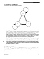
MOTOROLA
SEMICONDUCTOR
TECHNICAL INFORMATION
Signaling System 7
MPC860 SS7 Protocol Microcode
UserÕs Manual
Rev 1.2
July 2, 1997
Signaling System 7
Signaling System 7
1
SS7 Controller Overview
4
2
SS7 Controller Key Features
2.1
SS7 Channel Frame Transmission Processing
2.2
SS7 Channel Frame Reception Processing
2.3
SU filtering
2.3.1
Comparison Mask
2.3.2
Comparison State Machine
4
5
5
6
6
7
3
Microcode Use
3.1
Initialization Procedure
8
8
4
SS7 Memory Map
4.1
SS7-Specific Parameters
4.2
Configuring the General SCC Parameters
4.2.1
GSMR Register
4.2.2
DSR Register
4.2.3
MRBLR Register
8
8
10
10
10
10
5
SS7 Programming Model
5.1
SS7 Command Set
5.1.1
Transmit Commands
5.1.2
Receive Commands
5.2
Octet Counting mode
5.3
Error Monitor Operation
5.3.1
Alignment Error Monitor
5.3.2
Signal Unit Error Monitor
5.3.3
Definition of a good frame
5.3.4
Definition of an errored SU
5.4
SS7 Error Handling Procedure
5.4.1
Transmission Errors
5.4.2
Reception Errors
10
10
11
12
12
13
13
13
14
14
14
14
15
6
Registers
6.1
SS7 Event Register
6.2
SS7 Option Register
6.3
SS7 Mode Register (PSMR)
16
16
17
18
7
SS7 Rx Buffer Descriptor
19
8
SS7 Tx Buffer Descriptor
22
Appendix A - Microcode Initialization Procedure
24
2
Signaling System 7
1
2
3
Initialization Procedure for QUICC Revision $0001
Initialization Procedure for QUICC Revision $0002
Initialization Procedure for QUICC Revision $0003
24
24
25
Appendix B - SS7 Configuration Sequence
26
Appendix C - Performance Estimate
27
3
Signaling System 7
1 SS7 Controller Overview
Signaling System #7 (SS7) is a management protocol used in public switching networks.
The physical, data link, and network layer functions of the SS7 protocol are called the Message Transfer Part (MTP).
The data link layer portion of the MTP (layer 2) is based on HDLC frame formats. However,
SS7 at layer 2 also includes some unique functions that are difficult to implement using an
unaltered HDLC controller. These functions include: counting the number of octets by which
a frame is too long; the continuous sending and receiving of fill in signal units (FISUs) and
link status signal units (LSSUs); maintaining the SU Error Monitor; and filtering duplicate
back-to-back frames.
FISUs are 5 byte frames (three bytes plus 2 CRC bytes) that are sent continuously back-toback when no other data needs to be transmitted. LSSUs are also sent back-to-back during
the initial alignment of the protocol. LSSUs are 6 or 7 bytes long. SS7 also differs from other
HDLC-based protocols in that the closing flag of one frame can be the opening flag of the
next frame. Since these characteristics can make SS7 implementations very demanding,
the SS7 controller on the PowerQUICC provides additional help in these areas.
The SS7 controller enhances the basic HDLC functionality to include those additional layer
2 functions which are difficult, or time consuming to implement by an external processor.
This ss7 Controller microcode for the MPC860 is identical to the ss7 Controller microcode
for the MC68360.
2 SS7 Controller Key Features
¥ Uses either NMSI or TDM interface and a variety of data encoding schemes
¥ Flexible data buffers with multiple buffers per signal unit allowed
¥ Separate interrupts for received signal units and transmitted buffers
¥ Maintenance of good frame counter, Alignment Error Rate Monitor, and SU Error Monitor
¥ Standard HDLC features
ÑFlag/Abort/Idle generation/detection
ÑZero insertion/deletion
Ñ16-bit CRC-CCITT generation/checking
ÑDetection of non-octet aligned signal units
ÑProgrammable number of flags between signal units
¥ Detection of long SUs
¥ Discard short (less than 5 octets) signal units
¥ Automatic Fill-In Signal Unit transmission
¥ Automatic Link Status Signal Unit retransmission and reception
¥ Automatic discard of identical FISUs and LSSUs
MOTOROLA
4
Signaling System 7
¥ Octet Counting Mode support
¥ Command to force a reset of filtering state
¥ Command to force entry into octet counting mode
¥ Ability to permanently disable octet counting mode
¥ Ability to disable FISU and LSSU filtering
¥ Ability to force entry into octet counting mode if a receiver overrun occurs.
2.1 SS7 Channel Frame Transmission Processing
The SS7 Controller is designed to work with a minimum amount of intervention from the
PowerPC core. It operates in a similar fashion to the HDLC controller on the PowerQUICC,
but will automatically transmit a FISU if the current buffer descriptor is not ready.
When the core enables one of the transmitters and the first Buffer Descriptor has its ready
(R) bit set, the SS7 controller will fetch the data from memory and start transmitting the signal unit (after first transmitting the user-specified minimum number of flags between signal
units). When the end of the current BD has been reached, the CRC and the closing flag are
appended if the last (L) bit in Tx BD is set. (The TC bit in the Tx BD must be set to transmit
the CRC). If the RT bit is clear, the SS7 transmitter writes the signal unit status bits into the
BD and clears the Ready bit. If the I bit is set, the TXB event bit will be set in the event register. Thus, the I bit may be used to generate an interrupt after each buffer, after a group of
buffers, or after each signal unit (SU) has been transmitted.
If the RT bit in the Tx BD is set, the SS7 transmitter will retransmit the buffer descriptor until
the RT bit is cleared. The RT bit may be used for LSSU retransmission as well as FISU retransmission (though the controller will automatically send FISUs if the R bit is not set.)
The SS7 controller will then proceed to the next Tx BD in the table. If it is not ready, the SS7
controller will transmit FISUs with the first two octets (BSN, BIB, FSN and FIB fields) from
the previously transmitted signal unit. The SS7 transmitter samples the first two octets (BSN,
BIB, FSN and FIB fields) of every transmitted SU and stores this data in the internal RAM.
The SS7 transmitter will transmit FISUs continuously using the sampled two octets until the
next SU is ready for transmission. Thus, the user should prepare an SU in the transmit buffer
descriptor table before enabling the SS7 transmitter, otherwise the FISU will be transmitted
with a random first two octets.
If the user wishes to re-arrange the transmit queue before the CP has completed transmission of all buffers, the STOP TRANSMIT command should be issued. This can be useful for
transmitting expedited data before previously linked buffers or for error situations. The SS7
controller, when receiving the STOP TRANSMIT command, will stop transmitting and send
an ABORT (if it was in the process of transmitting a signal unit) and start transmitting Flags.
Alternately, the GRACEFUL STOP TRANSMIT command may be used to stop transmission
after the current frame completes. When the SS7 controller is given the RESTART TRANSMIT command, it resumes transmission.
MOTOROLA
5
Signaling System 7
2.2 SS7 Channel Frame Reception Processing
The SS7 receiver is also designed to work with a minimum amount of intervention from the
PowerPC core. The SS7 receiver can perform FISU/LSSU reception (and stripping), CRC
checking, maximum signal unit length checking, and minimum signal unit length checking
(SUs less than 5 octets). It can also provide interrupts the user on every N unstuffed octets
received while in Òoctet countÓ mode. The received signal unit is available to the user for performing any SS7-based protocol.
When the core enables one of the receivers, the receiver waits for an opening flag character.
When the receiver detects the first byte of the signal unit, the SS7 controller will fetch the
next Buffer Descriptor (BD) and, if empty, will start to transfer the incoming signal unit to the
BDs associated data buffer. When the data buffer has been filled, the SS7 controller clears
the Empty bit in the BD. If the incoming signal unit exceeds the length of the data buffer, the
SS7 controller will fetch the next BD in the table and, if empty, will continue to transfer the
rest of the signal unit to this BDÕs associated data buffer.
During this process the SS7 receiver will store the first five bytes of the SU in the internal
RAM. This data will be used to receive identical FISUs/LSSUs only twice. Signal Units that
have less than five octets will be discarded without notification to the user. The SS7 receiver
will check for a signal unit that is too long by comparing the SU length versus the MFLR register. If the SU is too long, the SS7 receiver enters the ÒOctet CountÓ mode. When the frame
ends, the CRC field is checked and written to the data buffer. The length of the entire signal
unit is written to the data length field of the last BD. The SS7 controller sets the last (L) bit,
writes the signal unit Status bits into the BD, and clears the Empty bit if the CM bit is clear.
It then sets the RXSU bit in the event register, indicating that a signal unit has been received
and is in memory. The SS7 controller then waits for a new signal unit.
The SS7 receiver will close a buffer and generate interrupt only when the first and second
FISU/LSSU is received. When the next FISU/LSSU is received and this FISU/LSSU is identical to the two previous FISUs/LSSUs, the FISU/LSSU will be discarded (stripped).
2.3 SU filtering
In order to reduce the overhead to the user software, a filtering algorithm has been adopted
to allow superfluous frames to be discarded. This algorithm compares the first 3-5 bytes
(depending on type) of the current FISU or LSSU to the last SU received and will discard if
it has already received that SU twice.
2.3.1 Comparison Mask
A user programmable 5-byte mask exists in the parameter RAM map. When an SU is received, the controller checks the contents of the LI field. If the value is between 0 and 2, the
SU (except for the CRC portion) will be masked according to the user programmable mask
and will then be compared to the last SU received. The state machine for the matching algorithm is in Section 2.3.2.
MOTOROLA
6
Signaling System 7
2.3.2 Comparison State Machine
The following state machine exists for filtering
0
2
1
¥ State 0 - The first 3-5 bytes (depending on the contents of the LI field) are masked and
then compared with the first 3-5 bytes of the last SU. If there is a match, go to State 1,
else remain in State 0. The current SU will be received into a Buffer Descriptor.
¥ State 1 - The first 3-5 bytes (depending on the contents of the LI field) are masked and
then compared with the first 3-5 bytes of the last SU. If there is a match, go to State 2,
else go to State 0. The current SU will be received into a Buffer Descriptor.
¥ State 2 - The first 3-5 bytes (depending on the contents of the LI field) are masked and
then compared with the first 3-5 bytes of the last SU. If there is a match, the current SU
will be discarded (unless there is an error) and the channel will remain in state 2. The
Error Free SU Counter will be incremented and the ERM will be adjusted accordingly.
If the frames do not match, the current SU will be received into a Buffer Descriptor and
the channel will return to State 0.
2.3.2.1 Filtering Limitations
Since the algorithm is purely checking IDENTICAL SUs, that means that TWO FISUs will be
received after each MSU rather than merely one, even though they have the same sequence numbers.
MOTOROLA
7
Signaling System 7
3 Microcode Use
The Signaling System 7 microcode must be loaded into PowerQUICC RAM at initialization
time. It will be a 'large' (1024 byte) microcode and thus will consume the memory area from
DPRAM_Base + $000 to DPRAM_Base + $3ff. In addition, the ÒMicrocode ScratchÓ area of
the memory map from DPRAM_Base + $600 to DPRAM_Base + $6FF will be unavailable
for user program use. (See Section 16.6 of the PowerQUICC User's Manual for more information)
3.1 Initialization Procedure
See appendix A for instructions on how to load and initialize the microcode.
4 SS7 Memory Map
4.1 SS7-Specific Parameters
When configured to operate in SS7 mode, the PowerQUICC overlays the structure illustrated listed in Table 16-23 of the PowerQUICC UserÕs Manual with the SS7-specific parameters described in Table 4-1.
Table 4-1. SS7-Specific Parameters
Address
SCC Base+34
SCC Base+38
SCC Base+3C
SCC Base+3E
SCC Base+40
SCC Base+42
SCC Base+44
SCC Base+46
SCC Base+48
SCC Base+4A
SCC Base+4C
SCC Base+4E
SCC Base+50
SCC Base+54
SCC Base+58
SCC Base+5A
SCC Base+5c
SCC Base+60
SCC Base+61
SCC Base+64
SCC Base+68
SCC Base+6a
Name
C_MASK
C_PRES
EFSUC
Reserved
MFLR
Temp
ERM
N
N_cnt
T
D
D_cnt
Temp
Temp
Temp
S7_OPT
Mask1
Mask2
Reserved
Temp
Temp
Temp
Width
Long
Long
Word
Word
Word
Word
Word
Word
Word
Word
Word
Word
Long
Long
Word
Word
Long
Byte
3 Bytes
Long
Word
Word
Description
CRC Constant
CRC Preset
Error Free SU Counter
Reserved
Max Frame (SU) Length Register
Temp
Error Monitor Counter
Interrupt Threshold in Octet Count Mode (N=16)
Temporary down counter for N
Parameter for ERM
Parameter for ERM
Parameter for ERM
Temp
Temp
Temp
SS7 Configuration Options
Mask for FISU Filtering
Mask for FISU FIltering
Temp
Temp
Temp
Note: Entries in boldface must be initialized by the user
C_MASK
This value should be initialized with $0000F0B8.
MOTOROLA
8
Signaling System 7
C_PRES
This value should be initialized with $0000FFFF.
EFSUC
This 16-bit counters is maintained by the CP. It may be initialized by the user while the
channel is disabled. The Error Free SU Counter is incremented whenever an error-free
SU is received (even if the frame is discarded by the filtering algorithm).
MFLR
Maximum Frame Length. This should be set to 278 for the Signaling System 7 protocol.
If a frame is received that is longer than MFLR, Octet Counting Mode will be entered.
Frame Length does not include the opening and closing flags.
ERM
This 16 bit counter is used for a leaky-bucket implementation of the SU Error Monitor and
the Alignment Error Monitor. It must be initialized to zero. This counter will not be updated
while the Error Monitor is disabled (using the bit in the SS7 Option Register).
N, N_cnt, D, D_cnt, T
The leaky bucket algorithm relies on three parameters. They are as follows:
¥ N, After every N octets are received while in octet counting mode, ERM will be incremented and the OCT bit in the SS7 Event Register will be set. N_cnt must be initialized
to the same value as N. N_cnt decrements at all times, whether the link is in octet counting mode or not.
¥ D, After D signal units (good or bad) or N octets in octet counting mode have been received, ERM will be decremented. ERM will not be decremented below zero. The D_cnt
parameter must be initialized to the same value as D. This counter is not used when the
Error Monitor is in Alignment Error Monitor mode. In addition, it will not be used when
the Error Monitor is disabled.
¥ T, If ERM reaches T, the ERM bit in the SS7 Event Register will be set and ERM will be
reset to zero.
S7_OPT
This is the location of the SS7 Option Register. It is described in Section 6.2.
Mask1, Mask2
This is the mask to be used for SU filtering. The mask should be in reverse-byte order.
Thus the format is:
MSBit
LSBit
Byte 4
Byte 3
Byte 2
Byte 1
Figure 4-1. Mask1 Format
MOTOROLA
9
Signaling System 7
MSBit
Byte 5
Figure 4-2. Mask2 Format
Note
This format is reversed from the normal Motorola byte storage
method. Also known as ÒLittle EndianÓ.
4.2 Configuring the General SCC Parameters
The general SCC parameters can be configured as described in section 16.14 of the PowerQUICC UserÕs Manual except for the following changes:
4.2.1 GSMR Register
The General SCC Mode Register bits are the same except for:
RTSMÑRTS Mode
0Ñ Do not use.
1Ñ Flags are transmitted between frames rather than idles. RTS is always asserted
whenever the SCC is enabled.
4.2.2 DSR Register
The SCC Data Synchronization Register should be programmed to $7E7E.
4.2.3 MRBLR Register
The Maximum Receive Buffer Length Register, like HDLC, must be evenly divisible by 4. In
addition, it must be 8 or larger in order for SU filtering to work properly.
5 SS7 Programming Model
The core configures each SCC to operate in one of the protocols by the MODE bits in the
GSMR. The SS7 controller uses the same data structure as in the other protocols. This data
structure supports multi-buffer operation.
The receive errors are reported through the Rx BD. The transmit errors are reported through
the Tx BD. An indication about the status of the lines (CD, and CTS) is reported through the
port C pins. A maskable interrupt may be generated upon a status change in either one of
those lines.
5.1 SS7 Command Set
The following commands are issued to the Command Register.
MOTOROLA
10
Signaling System 7
5.1.1 Transmit Commands
After a hardware or software reset and the enabling of the channel in the SCC mode register, the channel is in the transmit enable mode and starts polling the first BD in the table every 64 transmit clocks, or immediately if the TOD bit in the TODR is set.
STOP TRANSMIT Command
The STOP TRANSMIT command disables the transmission of frames on the transmit channel. If this command is received by the SS7 controller during frame transmission, transmission is aborted after a maximum of 16 additional bits are transmitted and the transmit FIFO
is flushed. The TBPTR is not advanced. No new BD is accessed and no FISUs are transmitted for this channel. The transmitter will transmit an abort sequence consisting of
Ò01111111Ó (if the command was given during frame transmission) and then begin to transmit flags.
NOTE
If the MFF bit in the PSMR is set, then it is possible for one or
more small frames to be flushed from the transmit FIFO. To
avoid this, the GRACEFUL STOP TRANSMIT command should
be used.
GRACEFUL STOP TRANSMIT Command
The GRACEFUL STOP TRANSMIT command is used to stop transmission in an orderly
way, rather than abruptly as performed by the regular STOP TRANSMIT command. It stops
transmission after the current frame has completed transmission, or immediately if there is
no frame currently being transmitted. The channel will not transmit FISUs. The GRA bit in
the SCCE will be set once transmission has stopped. After transmission ceases, the SS7
transmit parameters, including BDs, may be modified. The TBPTR will point to the next Tx
BD in the table. Transmission will begin once the Ready bit of the next BD is set and the
RESTART TRANSMIT command is issued.
RESTART TRANSMIT Command
The RESTART TRANSMIT command re-enables the transmission of characters on the
transmit channel. This command is expected by the SS7 controller after a STOP TRANSMIT
command, after a GRACEFUL STOP TRANSMIT command, or after a transmitter error. The
SS7 controller will resume transmission from the current transmitter BD (TBPTR) in the
channelÕs transmit BD table.
INIT TX PARAMETERS Command
Initializes all the transmit parameters in this serial channelÕs parameter RAM to their reset
state. This command must be issued before the transmitter is enabled for the first time. This
command should only be issued when the transmitter is disabled. Note that the INIT TX
AND RX PARAMETERS command may also be used to reset both transmit and receive parameters.
MOTOROLA
11
Signaling System 7
5.1.2 Receive Commands
After a hardware or software reset and the enabling of the channel by its SCC mode register,
the channel is in the receive enable mode and will use the first BD in the table.
ENTER HUNT MODE Command
The ENTER HUNT MODE command is generally used to force the SS7 receiver to abort
reception of the current frame and enter the hunt mode. In the hunt mode, the SS7 controller
continually scans the input data stream for the flag sequence. After receiving the command,
the current receive buffer is closed and the CRC is reset. Further frame reception will use
the next BD.
CLOSE RX BD Command
This command should not be used in the SS7 protocol.
INIT RX PARAMETERS Command
This command initializes all the receive parameters in this serial channelÕs parameter RAM
to their reset state. This command should only be issued when the receiver is disabled. Note
that the INIT TX AND RX PARAMETERS command may also be used to reset both receive
and transmit parameters.
RECEIVE NEXT SU Command
This command resets the filtering algorithm to ensure that the next SU will be received, even
if it would normally have been filtered. This command could be issued periodically so that
the CPU32+ can check to make sure that the link is really up and not simply receiving flags.
To issue this command, follow the procedure on page 7-7 but use an opcode of Ò1101Ó.
ENTER OCM Command
This command causes the channel to enter octet counting mode.
To issue this command, follow the procedure on page 7-7 but use an opcode of Ò1100Ó.
5.2 Octet Counting mode
The octet counting mode is used in SS7 to provide error management for the link. It is entered whenever a signal unit is received that is too long or when an ABORT signal is received (either at the end of a signal unit or between units). The Ôocm_ituÕ bit in the SS7
Option Register determines whether octet counting mode is entered if either of these two
conditions occur.
In addition, the SS7 controller has an option to allow octet counting mode to be entered if an
overrun error occurs. An overrun error occurs CP could not empty the receiver FIFO fast
enough and the FIFO overfilled. Another overrun condition is when the receiver could not
open a buffer in which to receive the current signal unit. In this case (the BUSY condition),
the SS7 controller will also enter octet counting mode. Since this is not included in the ITU
standard, this option is enabled separately using the Ôo_ornÕ bit in the SS7 Option Register.
MOTOROLA
12
Signaling System 7
The octet counter (the N and N_cnt parameters) is always running, even when the channel
is not in octet counting mode. When octet counting mode is entered by the controller, the
controller will update the ERM and generate an OCT interrupt whenever N_cnt decrements
to zero. Thus, the first OCT interrupt will occur between 1 and N octet times after entering
octet counting mode.
The SS7 controller will enter octet counting mode under the following circumstances:
¥ An ABORT character is received at any time and the o_itu bit is set in the SS7 Option
Register.
Note
The PowerQUICC SS7 controller does not differentiate between
an ABORT (01111111) and an IDLE (11111111) and thus assumes that seven consecutive ones are an ABORT.
¥ The SU currently being received has exceeded the length programmed in the MFLR
register and the o_itu bit is set in the SS7 Option Register.
¥ The receiver overruns and the o_orn bit is set in the SS7 Option Register.
¥ The receiver runs out of buffers (generating a BSY interrupt) and the o_orn bit is set in
the SS7 Option Register.
¥ The ENTER OCM command is issued.
The SS7 controller will leave the octet counting mode when a good frame is received (see
Section 5.3.3 for more information on the definition of a good frame)
5.3 Error Monitor Operation
The operation of the Error monitors is described in Figures 11, 17, and 18 of ITU Recommendation Q.703 (Signaling System No. 7 - Signaling Link).
5.3.1 Alignment Error Monitor
The Alignment Error Monitor (AERM) is used during initial link setup. It increments whenever
an error is detected. If the counter increments to T while the counter is active, the SS7 Controller set the ERM bit in the event register indicating that the AERM had reached the threshold.
5.3.2 Signal Unit Error Monitor
The Signal Unit Error Monitor (SUERM) is used once the link has been established. It is
used to monitor the error rate. The SUERM is decremented whenever D frames (good or
bad) are received. The SUERM increments whenever an errored SU is received or when an
OCT interrupt is generated indicating that N octets had been received in octet counting
mode.
MOTOROLA
13
Signaling System 7
Note
The ITU Q.703 specification differs from the Bellcore specification in how it handles the decrementing of the SUERM. The ITU
specification decrements the D_cnt parameter whenever a good
frame is received. The Bellcore specification decrements D_cnt
whenever a good frame is received AND the SUERM is non-zero. The SS7 Controller implements the ITU method.
5.3.3 Definition of a good frame
A good frame is one in which the length of the frame is greater than 4 and less than or equal
to the value in the MFLR parameter. A good frame also has a correct CRC value.
A frame can be considered good even if it is not received into a buffer descriptor. Any signal
units that are discarded by the filtering unit are still considered good frames. In addition, a
signal unit that is received without a receive buffer available (generating the BSY event) is
still considered a good frame unless the o_orn bit is set in the SS7 Option Register.
5.3.4 Definition of an errored SU
The SS7 controller considers any frame ÔerroredÕ that is not a good frame (as described in
Section 5.3.3) and does not result in the entry into octet counting mode (as described in Section 5.2). These errors include:
¥ DPLL Error
¥ CD lost error
¥ Overrun error (if the o_orn bit is not set in the SS7 Option Register)
¥ CRC Error
¥ Non-octet aligned error
5.4 SS7 Error Handling Procedure
The SS7 controller reports signal unit reception and transmission error conditions using the
channel BDs, the error counters, and the SS7 event register.
5.4.1 Transmission Errors
Transmitter Underrun
This error occurs because the contents of the transmitter FIFO were sent before more data
could be retrieved from memory. When this error occurs, the channel terminates buffer
transmission, sends the ABORT character, closes the buffer, sets the underrun (UN) bit in
the Tx BD, and sets the TXE bit in the SCC Event Register. The channel will resume transmission after the reception of the RESTART TRANSMIT command. The transmit FIFO size
is 32 bytes on SCC1 and 16 bytes on SCC2, SCC3, and SCC4.
Another type of transmitter underrun is when an SU is split over multiple transmit buffer descriptors and the last buffer is not ready when needed.
MOTOROLA
14
Signaling System 7
CTS Lost During Signal Unit Transmission
When this error occurs, the channel terminates buffer transmission, closes the buffer, sets
the Clear to Send lost (CT) bit in the Tx BD, and sets the TXE bit in the SCC Event Register.
The channel will resume transmission after the RESTART TRANSMIT command is given.
5.4.2 Reception Errors
Overrun Error
The SS7 controller maintains an internal 32 byte FIFO in SCC1 and 16 byte FIFO in the other SCCs for receiving data. A receive overrun occurs when the CP was unable to keep up
with the data rate or the SDMA channel was unable to write the received data to memory.
The previous data byte and the frame status are lost. The the controller closes the buffer
with the overrun (OV) bit in the BD set and sets the RXF bit in the SCC Event Register. The
receiver then enters the hunt mode. If the o_orn bit is set in the SS7 Option Register, the
controller will enter octet counting mode.
CD Lost During Signal Unit Reception
When this error occurs, the channel terminates signal unit reception, closes the buffer, sets
the Carrier Detect lost (CD) bit in the BD, and sets the RXF bit in the SCC event register.
This error has the highest priority. The rest of the signal unit is lost and other errors are not
checked in that signal unit. The receiver then enters the hunt mode and looks for the start
of the next signal unit.
Abort Sequence
An abort sequence is detected by the SS7 controller when 7 or more consecutive ones are
received. When this error occurs, the channel closes the buffer (if it was already open) by
setting the Rx Abort Sequence (AB) bit in the BD, and sets the RXF bit in the SCC Event
Register. The CRC and non-octet error status conditions are not checked on aborted signal
units. The SS7 receiver then enters octet count mode if the o_itu bit is set in the SS7 Option
Register. Finally, the receiver enters hunt mode and looks for the start of the next signal unit.
If an Abort sequence appears and the receiver is not in the middle of a signal unit, the receiver enters octet count mode if the o_itu bit is set in the SS7 Option Register.
Short Signal Unit (Less Than 5 Octets)
The SS7 controller will discard a short signal unit. The CRC and non-octet error status conditions are not checked on short signal units.
Non-octet Aligned Signal Unit
When this error occurs, the channel writes the received data to the data buffer, closes the
buffer, sets the Rx non-octet aligned signal unit (NO) bit in the BD, and sets the RXF bit in
the SCC Event Register. The CRC error status is not checked on non-octet signal units. After a non-octet aligned signal unit is received, the receiver enters Hunt mode and looks for
the start of the next signal unit.
MOTOROLA
15
Signaling System 7
CRC Error
When this error occurs, the channel writes the received CRC (Cyclic Redundancy Check)
to the data buffer, closes the buffer, sets the CR bit in the BD, and sets the RXF bit in the
SCC Event Register. After receiving a signal unit with a CRC error, the receiver enters Hunt
mode and looks for the start of the next signal unit.
6 Registers
6.1 SS7 Event Register
The SS7 Event Register is a 16-bit register which is used to report events recognized by the
SS7 channel and generate interrupts. Upon recognition of an event, the SS7 controller will
set the corresponding bit in the SS7 event register. Interrupts generated by this register may
be masked in the SS7 mask register.
The SS7 event register is a memory-mapped register that may be read at any time. A bit is
cleared by writing a one (writing a zero does not affect a bitÕs value). More than one bit may
be cleared at a time. All unmasked bits must be cleared before the CP will clear the internal
interrupt request. This register is cleared at reset.
15
14
13
12
GLr
11
GLt
10
DCC
9
FLG
8
IDL
7
GRA
6
OCT
5
SUER
4
TXE
3
RXS
2
BSY
1
TXB
0
RXB
Figure 4-3. SS7 Event Register
GLrÑGlitch on Rx
A clock glitch was detected by this SCC on the receive clock
GLtÑGlitch on Tx
A clock glitch was detected by this SCC on the transmit clock
DCCÑDPLL CS Changed
The carrier sense status as generated by the DPLL has changed state. The real-time status may be found in SCCS. This is not the CD pin status (which is reported in port C), and
is only valid when the DPLL is used.
FLGÑFlag Status
The SS7 controller has stopped or started receiving flags. The real-time status of the line
may be read in SCCS.
IDLÑIdle Sequence Status Changed
A change in the status of the serial line was detected. The real-time status of the line may
be read in SCCS.
GRAÑGraceful Stop Complete
A graceful stop, which was initiated by the GRACEFUL STOP TRANSMIT command, is
now complete. This bit is set as soon as the transmitter has finished transmitting any
MOTOROLA
16
Signaling System 7
frame that was in progress when the command was issued. It will be set immediately if no
frame was in progress when the command was issued.
OCTÑN Octets Received
If the channel is in Octet Count Mode, this bit is set after every N octets have been received.
SUERÑSU Error Monitor Threshold Reached
The SU Error Monitor has reached the programmed threshold.
TXEÑTx Error
An error (CTS lost or underrun) occurred on the transmitter channel.
RXSÑRx SU
A complete SU has been received on the SS7 channel. This bit is set no sooner than two
clocks after the receipt of the last bit of the closing flag.
BSYÑBusy Condition
An SU was received and discarded due to lack of buffers. Octet Counting mode was entered if enabled in the SS7 Option Register.
TXBÑTransmit Buffer
A buffer has been transmitted on the SS7 channel. This bit is set no sooner than when the
last bit of the closing flag begins its transmission if the buffer is the last one in the SU. Otherwise, this bit is set after that last byte of the buffer has been written to the transmit FIFO.
RXBÑRx Buffer
A Buffer has been received over the SS7 channel that was not a complete SU.
6.2 SS7 Option Register
The SS7 Option register is found in the SS7 Specific Parameters shown in Table 4-1. This
register is used to configure certain SS7-specific features of the microcode.
15
14
13
12
-
11
10
9
8
7
-
6
-
5
4
ermmd ermen
3
2
1
su_fil sen_fis o_orn
0
o_itu
Figure 4-4. SS7 Option Register
Bits 15-6ÑReserved, must be initialized to zero.
ermmdÑError Monitor Mode
0Ñ The Error Monitor is in SU Error Monitor Mode.
1Ñ The Error Monitor function is in Alignment Error Monitor Mode.
MOTOROLA
17
Signaling System 7
ermenÑError Monitor Enable
0Ñ The Error Monitor is disabled. The D, D_cnt, ERM, and T parameters may be modified while this bit is set to zero. The user must manually set this bit to zero when
an ERM event is generated.
1Ñ The Error Monitor is enabled.
su_filÑSU Filtering
0Ñ Do not filter SUs.
1Ñ Enable SU filtering.
sen_fisÑSend FISU if BD no ready
0Ñ FLAGs will be sent if the current BD does not have its ready bit set.
1Ñ FISUs will automatically be generated if the transmitter is enabled, the channel is
ready to transmit, and the current BD does not have its ready bit set.
o_ornÑOCM on Overrun
1Ñ Enter Octet Counting Mode if the SCCÕs FIFO overruns or if there are no BDs available.
o_ituÑOCM on ITU Conditions
1Ñ Enter Octet Counting Mode if an ITU defined reason for entering octet counting
mode occurs (Abort received, SU too long).
6.3 SS7 Mode Register (PSMR)
Each SS7 mode register is a 16-bit, memory-mapped, read-write register that controls SCC
operation. The term SS7 mode register refers to the PSMR of the SCC when that SCC is
configured in SS7 mode.
15
14
13
NOF
12
11
10
CRC
9
8
-
7
FSE
6
5
-
4
3
MFF
2
1
-
0
NOFÑNumber of Flags
Minimum number of flags between SUs or before SUs (0 to 15 flags). If NOF = 0000, then
no flags will be inserted between SUs. Thus, the closing flag of one SU will be immediately
followed by the opening flag of the next SU. These bits may be modified on the fly.
CRCÑCRC Selection
00Ñ 16-Bit CCITT-CRC (X16+X12+X5+1)
01Ñ Reserved
10Ñ Reserved
11Ñ Reserved
MOTOROLA
18
Signaling System 7
Bits 9,8ÑReserved, must be set to zero
FSEÑFlag Sharing Enable
This bit is only valid if the RTSM bit is set in the GSMR. This bit may be modified on the fly.
0Ñ Normal Operation
1Ñ If NOF(3:0) = 0000, then a single shared flag is transmitted between back-to-back
SUs. Other values of NOF are decremented by one when FSE is set.
Bits 6-4ÑReserved, must be set to zero
MFFÑMultiple Frames in FIFO
0Ñ Normal operation. The transmit FIFO can never contain more than one SS7 signal
unit. The CTS lost status will be reported accurately on a per-SU basis. The receiver is not affected by this bit.
1Ñ The transmit FIFO can contain multiple SUs, but CTS lost is not guaranteed to be
reported on the exact buffer/SU on which it truly occurred. This option, however,
can improve the performance of the SS7 transmissions in cases of small back-toback SUs or in cases where the user desires to strongly limit the number of flags
transmitted between frames. The receiver is not affected by this bit.
7 SS7 Rx Buffer Descriptor
The SS7 controller uses the Rx Buffer Descriptor (Rx BD) to report information about the
received data for each buffer. An example of the Rx BD process is shown in Figure 7-52 of
the UserÕs Manual.
The first word of the Rx BD contains control and status bits. Bits 12 to 15 and bit 9 are written
by the user; bits 0-7 and 10-11 are set by the CP following signal unit reception. Bit 15 is set
by the core when the buffer is available to the SS7 controller, and it is cleared by the SS7
controller when the buffer is full. The format of the control and status word is detailed below.
OFFSET + 0
OFFSET + 2
OFFSET + 4
OFFSET + 6
15
E
14
-
13
W
12
I
11
L
10
F
9
CM
8
7
6
5
DE
LG
DATA LENGTH
RX DATA BUFFER POINTER
4
NO
3
AB
2
CR
1
OV
0
CD
Note: Entries in boldface must be initialized by the user.
EÑEmpty
0Ñ The data buffer associated with this BD has been filled with received data, or data
reception has been aborted due to an error condition. The CPU32+ core is free to
examine or write to any fields of this Rx BD. The CP will not use this BD again while
the E-bit remains zero.
1Ñ The data buffer associated with this BD is empty, or reception is currently in
progress. This Rx BD and its associated receive buffer are owned by the CP. Once
the E-bit is set, the CPU32+ core should not write any fields of this Rx BD.
MOTOROLA
19
Signaling System 7
Bits 14, 8, 6ÑReserved, should be set to zero
WÑWrap (Final BD in Table)
0Ñ This is not the last buffer descriptor in the Rx BD table.
1Ñ This is the last buffer descriptor in the Rx BD table. After this buffer has been used,
the CP will receive incoming data into the first BD in the table (the BD pointed to
by RBASE). The number of Rx BDs in this table is programmable, and is determined only by the W-bit and the overall space constraints of the dual-port RAM.
IÑInterrupt
0Ñ The RXB bit in the SS7 Event Register will not be set after this buffer has been
used, but RXSU operation remains unaffected.
1Ñ The RXB or RXSU bit in the SS7 Event Register will be set when this buffer has
been used by the SS7 controller.
LÑLast in SU
This bit is set by the SS7 controller when this buffer is the last in an SU. This implies the
reception of a closing flag or reception of an error, in which case one or more of the CD,
OV, AB, and LG bits are set. The SS7 controller will write the number of SU octets to the
data length field.
0Ñ This buffer is not the last in an SU.
1Ñ This buffer is the last in an SU.
FÑFirst in SU
This bit is set by the SS7 controller when this buffer is the first in an SU.
0Ñ The buffer is not the first in an SU.
1Ñ The buffer is the first in an SU.
CMÑContinuous Mode
0Ñ Normal operation.
1Ñ The E-bit is not cleared by the CP after this BD is closed, allowing the associated
data buffer to be overwritten automatically when the CP next accesses this BD.
However, the E-bit will be cleared if an error occurs during reception, regardless of
the CM bit.
DEÑDPLL Error
This bit is set by the SS7 controller when a DPLL error has occurred during the reception
of this buffer. In decoding modes where a transition is promised every bit, the DE bit will
be set when a missing transition has occurred.
LGÑRx SU Length Violation
An SU length grater than the maximum defined for this channel was recognized (only the
maximum-allowed number of bytes (MFLR) is written to the data buffer). This event will
not be reported until the Rx BD is closed and the RXF bit is set (after the receipt of the
closing flag). However, Octet Count Mode will be entered automatically if enabled in the
MOTOROLA
20
Signaling System 7
SS7 Option Register. The actual number of bytes received between flags is written to the
data length field of this BD.
NOÑRx Non-octet Aligned SU
An SU that contained a number of bits not exactly divisible by eight was received
ABÑRx Abort Sequence
This BD was closed because an ABORT sequence (a minimum of seven consecutive
ones) was received during SU reception.
CRÑRx CRC Error
This SU contains a CRC error. The received CRC bytes are always written to the receive
buffer.
OVÑOverrun
A receiver overrun occurred during frame reception.
CDÑCarrier Detect Lost
The carrier detect signal was negated during frame reception. This bit is only valid when
working in the NMSI mode.
Data Length
Data length is the number of octets written by the CP into this BDÕs data buffer. It is written
by the CP once as the BD is closed.
When this BD is the last BD in an SU (L=1), the data length contains the total number of
SU octets (including the 2 bytes for CRC).
The actual amount of memory allocated for this buffer should be greater than or equal to
the contents of the MRBLR.
Rx Data Buffer Pointer
The receive buffer pointer, which always points to the first location of the associated data
buffer, may reside in either internal or external memory. The Rx buffer pointer must be
divisible by 4.
MOTOROLA
21
Signaling System 7
8 SS7 Tx Buffer Descriptor
Data is presented to the SS7 controller for transmission on an SCC channel by arranging it
in buffers referenced by the channelÕs TX BD table. The HDLC controller confirms transmission (or indicates error conditions) using the BDs to inform the CPU32+ core that the buffers
have been serviced.
OFFSET + 0
OFFSET + 2
OFFSET + 4
OFFSET + 6
15
R
14
-
13
W
12
I
11
L
10
TC
9
RT
8
7
6
DATA LENGTH
TX DATA BUFFER POINTER
5
-
4
-
3
-
2
-
1
UN
0
CT
Note: Entries in boldface must be initialized by the user
RÑReady
0Ñ The data buffer associated with this BD is not ready for transmission. The user is
free to manipulate this BD or its associated data buffer. The CP clears this bit after
the buffer has been transmitted or after an error condition is encountered.
1Ñ The data buffer, which has been prepared for transmission by the user, has not
been transmitted or is currently being transmitted. No fields of this BD may be written once this bit is set.
Bits 14, 8-2ÑReserved, should be set to zero
WÑWrap (Final BD in Table)
0Ñ This is not the last buffer descriptor in the Tx BD table.
1Ñ This is the last buffer descriptor in the Tx BD table. After this buffer has been used,
the CP will transmit from the first BD in the table (the BD pointed to by TBASE).
The number of Tx BDs in this table is programmable, and is determined only by the
W-bit and the overall space constraints of the dual-port RAM.
IÑInterrupt
0Ñ The TXB bit in the SS7 Event Register will not be set after this buffer has been
used.
1Ñ The TXB bit in the SS7 Event Register will be set when this buffer has been transmitted by the SS7 controller.
LÑLast
0Ñ This is not the last buffer in the current SU.
1Ñ This is the last buffer in the current SU.
TCÑTx CRC
This bit is only valid when the L-bit is set; otherwise, it is ignored.
0Ñ Transmit the closing flag after the last data byte. This setting can be used for testing purposes to send a bad CRC after the data.
1Ñ Transmit the CRC sequence after the last data byte.
MOTOROLA
22
Signaling System 7
RTÑRetransmit
0Ñ Normal operation.
1Ñ The R-bit is not cleared by the CP after this BD is closed. The CP will repeat transmission of this BD until the RT bit is cleared. After the RT bit is cleared, the CP will
progress to the next BD in the table. However, the R-bit will be cleared (and the CP
will progress to the next BD in the table) if an error occurs during transmission, regardless of the RT bit.
Note
This bit behaves differently than the ÒCMÓ bit which is usually located in this position and is found in the Rx BD.
The following status bits are written by the SS7 controller after it has finished transmitting
the associated data buffer.
UNÑUnderrun
The SS7 controller encountered a transmitter underrun condition while transmitting the
associated data buffer.
CTSÑCTS Lost
CTS in NMSI mode was lost during frame transmission. If data from more than one buffer
is currently in the FIFO when this error occurs, this bit will be set in the TX BD that is currently open.
Data Length
Data length is the number of bytes the SS7 controller should transmit from this BDÕs data
buffer. It is never modified by the CP. The value of this field must be greater than zero.
Note
If you are using the Òauto FISU transmissionÓ option, the first two
octets of each frame may not reside in two different buffers.
Tx Data Buffer Pointer
The transmit buffer pointer, which contains the address of the associated data buffer, may
be even or odd. The buffer may reside in either internal or external memory. This value is
never modified by the CP.
MOTOROLA
23
Signaling System 7
Appendix A - Microcode Initialization Procedure
The initialization procedure does not vary with the revisions of the PowerQUICC ROM (this
statement was true at time the manual was written). The microcode itself does vary, and the
user needs to make sure he downloads the correct version of microcode into the chip.
Be sure to check the Rev_Num register in the Misc_Base area (see table 16-1 in PowerQUICC UserÕs manual) to determine which revision of microcode to use.
At the time this document was written there were two versions of the ss7 microcode:
Mask Number Revision Misc_Base value Microcode Rev
Rev 0
0001
rev_03
E64C
Rev
A
0003
rev_a2
F84C
1 Initialization Procedure for PowerQUICC
The microcode package includes a basic driver written in ÔcÕ code that runs on the MPC860
ADS board. The driver is not a full blown test of the ss7 functionality, but it is a simple demonstration code. It shows how to initialize the registers in the MMPC860, to enable the ss7
microcode. This code is intended to be used as a quick reference to speed up the integration
of the ss7 code in the target application software.
One of the ÔcÕ code files provided is named: Ôucodednld.cÕ
This file contains the microcode in the from of two arrays. The arrays are called
Ôss7_ucode_1Õ and Ôss7_ucode_2Õ. These arrays contain the CPM opcodes for the ss7 microcode, and they need to be copied to the Dual Ported RAM.
There is also a ÔcÕ code routine called Ôss7_load_microcodeÕ that copies the two arrays into
the Dual ported RAM. At the end, this routine initializes the trap registers as necessary. The
ucodednld.c file can be compiled with the target application software, or it can be used as a
reference.
Initialization procedure:
1. Download the supplied binary opcodes (in file ucodednld.c) into the Dual Ported RAM.
Array ss7_ucode_1 is copied starting at address DPRAM_Base+$000. Array
ss7_ucode_2 is copied starting at address DPRAM_Base+$F00. On the MPC860
ADS board those address are $2202000 and $2202F00 respectively.
2. Write $8066 to IMMR+ $9CC (CPCR1)
MOTOROLA
24
Signaling System 7
3. Write $8046 to IMMR+ $9CE (CPCR2 register)
4. Write $8C15 to IMMR+ $9D0 (CPCR3 register)
5. Write $8C16 to IMMR+ $9D2 (CPCR4 register)
6. Write $0002 to IMMR+ $9c4 (RCCR register)
7. Write $8000 to IMMR+ $9c0 (CPCR register)
Note
If the PowerQUICC is ever reset, the microcode must be reloaded and reinitialized.
MOTOROLA
25
Signaling System 7
Appendix B - SS7 Configuration Sequence
The following list is a suggested initialization sequence when using SS7. This assumes that
the initialization sequence described in Section 3.1 has already been performed.
1. Initialize the SDCR register.
1. Configure Port A and Port C pints to enable RXD, TXD, CTS, CD, and CTS. (This assumes you are using NMSI mode. If not, appropriately configure the time slot assigner
and TSA pins)
2. Configure a BRG to generate appropriate channel clocking frequency.
3. Program the SICR to route the BRG clocking to the SCC running SS7.
4. Select whether the channel is using the Time Slot Assigner or the NMSI pins in the
SICR.
5. Write RBASE and TBASE in the SCCÕs parameter RAM to point to the first RxBD and
the first TxBD.
6. Issue the INIT RX & TX PARAMETERS command for that SCC.
7. Program RFCR and TFCR.
8. Write MRBLR with the maximum receive buffer size. (see Section 4.2.3)
9. Write C_MASK and C_PRES with the standard values.
10. Write the MFLR register to the standard SS7 value.
11. Clear the SU counter (EFSUC).
12. Program the SU Error Monitor parameters (N, N_cnt, D, D_cnt, and T).
13. Clear the Error Monitor (ERM).
14. Write the desired Mask1 and Mask2 values for the FISU filtering algorithm.
15. Initialize all RxBDs.
16. Initialize all TxBDs.
17. Clear the SCCE register by writing $FFFF to it.
18. Program the SCCM register with the proper mask to allow all desired interrupts.
19. Program the DSR register (see Section 4.2.2)
20. Program the GSMR_H. (see Section 4.2.1)
21. Program the GSMR_L register to SS7 mode, but do not turn on the transmitter or receiver.
22. Set the PSMR register appropriately. (see Section 6.3)
23. Set the SS7 Option Register. (see Section 6.2)
24. Turn on the transmitter and receiver in the GSMR_L register.
MOTOROLA
26
Appendix C - Performance Estimate
Since SS7 is typically a low-speed protocol (64 Kbit links), the data rate for each link can
easily be handled by the CPM. It is estimated that the CPM could handle a much higher
speed link with ease but no performance tests have been done to verify this capability. Below is an estimate of the maximum performance of the PowerQUICC when the SS7 controller is being used.
At 25 MHz, an aggregate SS7 bandwidth of approximately 6 Mbps divided among the 4
SCCs consumes 100% of the processing power of the RISC communications engine. If only
a percentage of the total available SS7 bandwidth is used, the remaining RISC processing
power can be used to run other protocols on other channels.
SS7 Channels
1 x 64 Kbit/s
2 x 64 Kbit/s
3 x 64 Kbit/s
Risc Bandwidth
Consumed (est)
1%
2%
3%
Possible Configuration of Other Channels
1 x 10 Mbit Ethernet, 2 x 2.048 Mbit HDLC
2 x 4 Mbit HDLC, 2 x 19.2 Kbit SMC UART
1 x 6 Mbit HDLC, 2 x 19.2 Kbit SMC UART
NOTE: The QUICC can support a maximum of 4 channels of SS7.
27
MOTOROLA
HOW TO REACH US:
USA/EUROPE/LOCATIONS NOT LISTED:
Motorola Literature Distribution
P.O. Box 5405
Denver, Colorado 80217
1-800-521-6274 or 480-768-2130
JAPAN:
Motorola Japan Ltd.
SPS, Technical Information Center
3-20-1, Minami-Azabu, Minato-ku
Tokyo 106-8573, Japan
81-3-3440-3569
ASIA/PACIFIC:
Motorola Semiconductors H.K. Ltd.
Silicon Harbour Centre
2 Dai King Street
Tai Po Industrial Estate
Tai Po, N.T., Hong Kong
852-26668334
HOME PAGE:
http://motorola.com/semiconductors
Information in this document is provided solely to enable system and software implementers to use Motorola products.
There are no express or implied copyright licenses granted hereunder to design or fabricate any integrated circuits or
integrated circuits based on the information in this document.
Motorola reserves the right to make changes without further notice to any products herein. Motorola makes no warranty,
representation or guarantee regarding the suitability of its products for any particular purpose, nor does Motorola assume
any liability arising out of the application or use of any product or circuit, and specifically disclaims any and all liability,
including without limitation consequential or incidental damages. “Typical” parameters that may be provided in Motorola
data sheets and/or specifications can and do vary in different applications and actual performance may vary over time. All
operating parameters, including “Typicals”, must be validated for each customer application by customer’s technical
experts. Motorola does not convey any license under its patent rights nor the rights of others. Motorola products are not
designed, intended, or authorized for use as components in systems intended for surgical implant into the body, or other
applications intended to support or sustain life, or for any other application in which the failure of the Motorola product could
create a situation where personal injury or death may occur. Should Buyer purchase or use Motorola products for any such
unintended or unauthorized application, Buyer shall indemnify and hold Motorola and its officers, employees, subsidiaries,
affiliates, and distributors harmless against all claims, costs, damages, and expenses, and reasonable attorney fees arising
out of, directly or indirectly, any claim of personal injury or death associated with such unintended or unauthorized use, even
if such claim alleges that Motorola was negligent regarding the design or manufacture of the part.
MOTOROLA and the Stylized M Logo are registered in the US Patent and Trademark Office. All other product or service
names are the property of their respective owners. Motorola, Inc. is an Equal Opportunity/Affirmative Action Employer.
© Motorola Inc. 1997
MPC860SS7UM/D
Rev. 1.2
7/1997