1
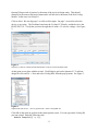
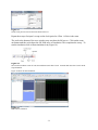
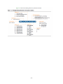
EE 254
Notes on Quartus and ModelSim
Spring 2013
These notes illustrate how to use Quartus 12.1 to create a simple project in Verilog, simulate it in
ModelSim, and load it onto the DeoNano board.
The professional version of Quartus II 12.1 and Nios II 12.1 are available on the lab computers.
At this time we have only the free version of ModelSim. You can get web versions of all of the
software from Altera for use on your own computer. We will not be using Nios II in this class.
Here are the links.
https://www.altera.com/download/software/quartus-ii-we For web edition of Quartus II
https://www.altera.com/download/software/modelsim-starter/12.1 For ModelSim Starter edition
v10.0c Software Download for Quartus II v12.1
If you have a slow internet connection, you can get a dvd from the instructor that has the needed
files on it.
This example creates a Verilog file which describes an AND gate. We will load the compiled file
to the DeoNano board where the inputs to the AND gate will be the two push button switches and
the output will be one of the onboard LEDs. To complete this example you will need: Quartus
12.1, ModelSim, the DeoNano board, and the USB programming cable for the board.
Quartus II
Begin by opening Quartus II. Close the opening Quartus II flash screen and click on File →
New Project Wizard. Click on Next on the intro screen. On page 1 of the wizard, use the
browse button to find a new location for your project. If necessary create a new folder. It is
always best to keep each project in its own folder. Name your project Example1. On my
computer the final screen looks like Figure 1.
Figure 1
Page 1 of the project wizard.
-1-
Quartus II keeps track of projects by the name of the top level design entity. This should
generally be the same as the project name and it will need to be the name of the first Verilog
module. In this case it is Example1.
Click on Next. We can skip page 2 so click on Next again. On page 3 we need to select the
device we are using. The DeoNano board uses the Cyclone IV E family and the device is the
EP4CE22F17C6. Verify that you have the right device with a 1.2 volt core voltage. See Figure
2.
Figure 2
Select the Cyclone IV E family and the EP4CE22F17C6 device for the DeoNano board.
At this point we are done with the wizard. Click Finish to get back to Quartus II. To add our
design file click on File → New and select Verilog HDL from the pop-up menu. See Figure 3.
Figure 3
In Quartus II click on File → New to get this menu. Select Verilog HDL file.
Click OK on the menu to get back to the main Quartus screen. You can type on the Verilog file
you just created. Enter the following code.
module Example1(f, a, b);
-2-
input a, b;
output f;
and A1(f, a, b);
endmodule
Click on File → SaveAs and save the file as Example1.v
Note that this is our top level module so it must be named Example1.v. If we give it any other
name the compile will fail. Also be careful of the semicolons. Unlike C there is a semicolon
after the module declaration and there is no semicolon after the endmodule statement – it's crazy
but live with it!
To compile the saved program click on Processing → Compile. This takes several seconds.
When it is done you may have several warnings but you should have no errors. If you have
errors you have entered something incorrectly and it must be corrected before you go on. The
warnings have to do with the fact that this project has not clock defined and that we have not
assigned any pins. For now these warnings can be ignored. You should get a Flow Summary of
the compile that looks something like that in Figure 4.
Figure 4
The compiler report from a successful compile.
Pin Assignments
Click on Processing → Start → Analysis and Elaboration. This step prepares the file for the pin
assignments. When this completes click on OK.
Choose Assignments → Pin Planner. The pin planner opens as shown in Figure 5. We use the
pin planner to connect the inputs and the output of the Verilog code the physical pins on the chip.
This is a wire-bond chip which means the pins are on the bottom. They are arranged in rows and
columns and that's how we refer to them. From the DeoNano documentation we find that the
two push-buttons (called Key[0] and Key[1]) are located on pins J15 and E1. There are eight
-3-
LEDs and the first one (LED[0]) is located on A15. We need to enter these pin locations in the
location column on the pin planner. See Figure 6.
Figure 5
The pin planner (left) and the pins located in rows and columns (right).
Figure 6
Fill in the pin locations for the two push-buttons and the LED.
Timing File
Every project needs to have a timing file – even in this case where it is meaningless. The file is
called a Synopsis Design Constraint file and has an sdc extension.
Chose Tools → TimeQuest Timing Analyzer. Ignore the welcome screen and in the Analyzer
click on File → new SDC file. This will open the SDC editor. You will have to minimize the
Timing Analyzer to see it. In the SDC file enter the single line derive_clock_uncertainty. Save
the file as Example1.sdc.
-4-
Note that if you do not include this file you will get a critical warning which can be ignored. For
applications where clock parameters and speed are critical you can use the Timing Analyzer to
set up specific clock parameters and Quartus will determine whether or not those parameters can
be met for your implementation. For most projects in this class, and sdc file can be omitted and
the resulting warning ignored.
Final Compile
Now that the pins have been assigned we can do a final compile which will create an SRAM
object file (SOF) which can be loaded into the DeoNano board. Click on Processing → Start
Compilation. You will have fewer warnings this time since the pin assignments have been
resolved. Ignore the other warnings.
Programming the DeoNano board
In order to program the DeoNano board you need the USB-Blaster driver for the USB port. This
driver comes with the Quartus II software. See p. 38 of the Deo-Nano user's manual (on the CD)
for instructions as to how to load this driver. With the driver installed, connect the USB cable to
your computer and the DeoNano board. In Quartus, click on Tools → Programmer. This will
produce the screen shown in Figure 7. If the .sof file is not shown on the screen window, click
on Add File and find it under Example1/output_files.
Figure 7
Click on Tools → Programmer to get this programming screen.
In the programmer click on Hardware Setup to get the screen shown in Figure 8. Click on the
Hardware Settings tab and use the drop down box to select USB-Blaster [USB-0]. Click on
Close to go back to the screen shown in Figure 7. Click on Start to begin programming.
-5-
Figure 8
Setting up the hardware for the USB blaster.
The programming takes only a short time. When it is done you will see that the blue light and
one green LED turned on for the DeoNano board. Recall that the design file with the Verilog
code was a simple AND gate for the two push-buttons. When the push-buttons are not pushed,
they are in the logical 1 state. Push either button to get the LED to go off. Congratulations!
You have just used several thousand programmable gates to implement the AND function.
ModelSim
You can turn the hardware off and you can close Quartus. Neither is needed for simulation in
ModelSim. ModelSim is a separate program from Quartus which is made by Mentor Graphics.
The current free version is 10.0c.
Before you begin the simulation you should create a new folder to hold the simulation files. You
need to copy Example1.v into this folder. After moving Example1.v into this new folder open it
in a text editor (like WordPad) and add a single line to the beginning to specify time precision.
The modified file looks like this:
`timescale 1ns/100ps
module Example1(f, a, b);
input a, b;
output f;
and A1(f, a, b);
endmodule
The timescale directive begins with a diacritical mark (a grave accent mark at the top left of the
keyboard) and it specifies the time units/time precision. For this example we have units of nanoseconds with a precision of 100 pico-seconds.
Open ModelSim. Close the splash screen and click on File → Change Directory. Browse to the
directory you created that has Example1.v in it. Click on File → New → Library. This opens a
dialog box as shown in Figure 9.
-6-
Figure 9
The new library dialog box.
You can rename the library but its best to just leave it as the default work. Click on OK. The
simulator can now be used to compile the design file. It will place results in the new library.
Select Compile → Compile. In the dialog box that pops up select Example1.v and click on the
Compile button. This will compile Example1.v in about two seconds. Click on done and notice
that the work file is no longer empty. Click on the + sign next to work to expand the folder and
double click on Example1.v to load it into the simulator. The screen shown in Figure 10 appears.
Figure 10
The simulation screen.
The simulation screen consists of three windows. (These three windows may not be arranged the
same as they are in Figure 10.) The leftmost is called the Structure window and it is labeled Sim.
The Structure window shows the organization of the design. In this example, it's not much but
other more complex examples will have many modules. The center window is the Objects
window. Note that it has all of the variables in the design file. The right most window is the
Wave window and this is where ModelSim shows the results of simulation. Any of the three
windows can be opened or closed in the View menu.
To do the simulation we need to add the signals to the Wave window. Do this by right-clicking
on Example1 in the Sim window. Select Add → To Wave → All Items in Region. At the top
-7-
center of the screen is a small window that has the run length. In Figure 10 it is set to 100 ps.
Change this to 1000 ns. Your screen should look like that shown in Figure 11.
Figure 11
Right click on Example1 and select Add → To Wave → All Items in the Region.
You could run the simulation at this point but you would get nothing very meaningful from the
run since none of the inputs have been assigned a value. To create input signal values for
simulation we need to use the Waveform Editor. For this example there are two inputs called a
and b. Right click on the a input in the Object window and select Modify → Apply wave. A
menu pops up as shown in Figure 12.
Figure 12
The wave pattern creator for input a.
Set the end time to 1000 ns (not ps) and select a Clock pattern. Click Next to get the window in
Figure 13. In this window set the clock period to 100 ns and set the initial value to 0. Click on
Finish.
-8-
Figure 13
Set the clock period to 100 ns and set the initial value to 0.
Repeat these steps for input b except set the clock period to 150ns. All else is the same.
The scale at the bottom of the wave window may not show the full waves. Click on the zoom
out button until the scale shows the full 1000 nsecs of simulation. This completes the set up. To
run the simulation click on Run simulation icon (Figure 14).
Figure 14
Run runs the simulation. Run-All runs the simulation until it hits a break. Continue Run runs after a break. Break
stops simulation.
Figure 15 shows the final simulation.
Figure 15
End result of simulation.
-9-
Reference Information
Pin Name
Pushbutton [0]
Pushbutton [1]
LED[0]
LED[1]
LED[2]
LED[3]
LED[4]
LED[5]
LED[6]
LED[7]
CLOCK_50
Switch 0
Switch 1
Switch 2
Switch 3
FPGA Pin Location
J15
E1
A15
A13
B13
A11
D1
F3
B1
L3
R8
M1
T8
B9
M15
-10-
-11-