1
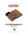
MSP430-5510STK development board
USER’S MANUAL
Revision C, November 2012
Designed by OLIMEX Ltd, 2011
All boards produced by Olimex LTD are ROHS compliant
OLIMEX© 2012
MSP430-5510STK User's Manual
Disclaimer:
© 2012 Olimex Ltd. Olimex®, logo and combinations thereof, are registered trademarks of Olimex Ltd. Other terms
and product names may be trademarks of others.
The information in this document is provided in connection with Olimex products. No license, express or
implied or otherwise, to any intellectual property right is granted by this document or in connection with the sale
of Olimex products.
Neither the whole nor any part of the information contained in or the product described in this document may be
adapted or reproduced in any material from except with the prior written permission of the copyright holder.
The product described in this document is subject to continuous development and improvements. All particulars of the
product and its use contained in this document are given by OLIMEX in good faith. However all warranties implied or
expressed including but not limited to implied warranties of merchantability or fitness for purpose are excluded. This
document is intended only to assist the reader in the use of the product. OLIMEX Ltd. shall not be liable for any loss or
damage arising from the use of any information in this document or any error or omission in such information or any
incorrect use of the product.
This evaluation board/kit is intended for use for engineering development, demonstration, or evaluation purposes only
and is not considered by OLIMEX to be a finished end-product fit for general consumer use. Persons handling the
product must have electronics training and observe good engineering practice standards. As such, the goods being
provided are not intended to be complete in terms of required design-, marketing-, and/or manufacturing-related
protective considerations, including product safety and environmental measures typically found in end products that
incorporate such semiconductor components or circuit boards.
Olimex currently deals with a variety of customers for products, and therefore our arrangement with the user is not
exclusive. Olimex assumes no liability for applications assistance, customer product design, software performance, or
infringement of patents or services described herein.
THERE IS NO WARRANTY FOR THE DESIGN MATERIALS AND THE COMPONENTS USED TO
CREATE MSP430-5510STK. THEY ARE CONSIDERED SUITABLE ONLY FOR MSP430-5510STK.
Thank you for purchasing MSP430-5510STK development board assembled by
OLIMEX LTD.
Page 2 of 26
OLIMEX© 2012
MSP430-5510STK User's Manual
Table of Contents
CHAPTER 1: OVERVIEW........................................................................................5
1. Introduction to the chapter.......................................................................................................5
1.1 Features.....................................................................................................................................5
1.2 Organization.............................................................................................................................6
CHAPTER 2: SETTING UP THE MSP430-5510STK BOARD.............................7
2. Introduction to the chapter.......................................................................................................7
2.1 Electrostatic warning...............................................................................................................7
2.2 Requirements...........................................................................................................................7
2.3 Powering the board..................................................................................................................8
2.4 Prebuilt software......................................................................................................................8
2.5 Bootloader mode......................................................................................................................8
CHAPTER 3: MSP430-5510STK BOARD DESCRIPTION..................................9
3. Introduction to the chapter.......................................................................................................9
3.1 Layout (top view).....................................................................................................................9
CHAPTER 4: THE MSP430F5510 MICROCONTROLLER..............................10
4. Introduction to the chapter.....................................................................................................10
4.1 The microcontroller...............................................................................................................10
5. Introduction to the chapter.....................................................................................................12
5.1 Reset........................................................................................................................................12
5.2 Clocks......................................................................................................................................12
CHAPTER 6: HARDWARE.....................................................................................13
6. Introduction to the chapter.....................................................................................................13
6.1 Battery connector...................................................................................................................13
6.2 JTAG connector.....................................................................................................................13
6.3 UEXT......................................................................................................................................14
6.4 Pads on the proto area...........................................................................................................15
6.5 USB mini connector...............................................................................................................16
6.6 SD/MMC slot..........................................................................................................................16
6.7 Jumper description................................................................................................................17
6.8 LCD Display...........................................................................................................................18
6.9 Additional hardware components........................................................................................18
CHAPTER 7: MEMORY AND BLOCK DIAGRAM............................................19
7. Introduction to the chapter.....................................................................................................19
7.1 Memory organization............................................................................................................20
CHAPTER 8: SCHEMATICS..................................................................................21
8. Introduction to the chapter.....................................................................................................21
Page 3 of 26
OLIMEX© 2012
MSP430-5510STK User's Manual
8.1 Eagle schematic......................................................................................................................21
8.2 Physical dimensions...............................................................................................................23
CHAPTER 9: REVISION HISTORY.....................................................................24
9. Introduction to the chapter.....................................................................................................24
9.1 Document revision.................................................................................................................24
9.2 Web page of your device.......................................................................................................25
9.3 Product support.....................................................................................................................26
Page 4 of 26
OLIMEX© 2012
MSP430-5510STK User's Manual
CHAPTER 1: OVERVIEW
1. Introduction to the chapter
Thank you for choosing the MSP430-5510STK development board from Olimex! This document
provides a User’s Guide for the Olimex MSP430-5510STK development board. As an overview,
this chapter gives the scope of this document and lists the board’s features. The document’s
organization is then detailed.
The MSP430-5510STK development board enables code development of applications running on
the MSP430F5510 microcontroller, manufactured by Texas Instruments.
1.1 Features
•
MCU MSP430F5510 with 32K Bytes Program Flash, 4K Bytes RAM, 25Mhz LCD display
8 alphanumeric
micro SD card connector
•
•
LiPo battery on board charger
USB connector, and USB bootloader support
•
•
two buttons
2 status LEDs
•
•
access to every pin near prototype area
Reset button
•
•
UEXT connector that allows other Olimex's modules (MOD-MP3, MOD-NRF24L01, etc.)
to be connected
JTAG connector
•
•
JTAG Power_In and Power_Out jumpers
32 768 Hz oscillator crystal
•
•
4 Mhz crystall oscillator
Power supply voltage regulators and filtering capacitor
•
•
Power on Led
PCB: FR-4, 1.5 mm (0,062"), soldermask, white silkscreen component print
•
Dimensions: 100x 80mm (3.94x 3.14")
•
Page 5 of 26
OLIMEX© 2012
MSP430-5510STK User's Manual
1.2 Organization
Each section in this document covers a separate topic, organized as follow:
– Chapter 1 is an overview of the board usage and features
–
–
Chapter 2 provides a guide for quickly setting up the board
Chapter 3 contains the general board diagram and layout
–
Chapter 4 describes the component that is the heart of the board: the MSP430F5510
microcontroller
Chapter 5 is an explanation of the control circuitry associated with the microcontroller to
reset. Also shows the clocks on the board
–
–
–
Chapter 6 covers the connector pinout, peripherals and jumper description
Chapter 7 shows the processor diagram and memory map
–
–
Chapter 8 provides the schematics
Chapter 9 contains the revision history
Page 6 of 26
OLIMEX© 2012
MSP430-5510STK User's Manual
CHAPTER 2: SETTING UP THE MSP430-5510STK BOARD
2. Introduction to the chapter
This section helps you set up the MSP430-5510STK development board for the first time.
Please consider first the electrostatic warning to avoid damaging the board, then discover the
hardware and software required to operate the board.
The procedure to power up the board is given, and a description of the default board behavior is
detailed.
2.1 Electrostatic warning
MSP430-5510STK is shipped in a protective anti-static package. The board must not be exposed to
high electrostatic potentials. A grounding strap or similar protective device should be worn when
handling the board. Avoid touching the component pins or any other metallic element.
2.2 Requirements
In order to set up the MSP430-5510STK, the following items are required:
- A source of power – the board can be powered through the mini USB connector (standard 5V) or
through the JTAG connector.
- Programmer supporting 14 pin JTAG interface and the used microcontroller MSP430F5510.
All our MSP programmers are recommended with MSP430-5510STK:
- Olimex MSP430-JTAG-ISO – isolated emulator/programmer USB<->JTAG 14p
- Olimex MSP430-JTAG-TINY – small emulator/programmer USB<->JTAG 14p
- Olimex MSP430-JTAG-RF – wireless emulator/programmer USB<->JTAG 14p
Also, a host-based software toolchain is required in order to program/debug the MSP430-5510STK
board. There are also a number of ready IDEs available like IAR Embedded Workbench, Rowley
CrossWorks, Code Composer Studio, etc.
We also provide our own flash programming software which can be distributed free. You can find it
at the device web page.
Page 7 of 26
OLIMEX© 2012
MSP430-5510STK User's Manual
2.3 Powering the board
-Plug mini USB with at least 5V to the board.
OR
-Set the jumpers P_IN closed, P_OUT open so you can power from JTAG connector
On powering the board via USB the PWR LED, LED1 and the display should turn on.
On powering the board via JTAG the LED1 and the display should turn on.
Note that the battery connector cannot power the board! It is used for charging 3.7V Lithium
batteries only.
2.4 Prebuilt software
On powering the board via the USB the PWR LED should turn on. The LED1 should blink green
and the LCD should show the message: “OLIMEX”.
2.5 Bootloader mode
To enter bootloader mode press USB_BSL button and then plug the board. You will also need the
correct bootloader software which is available at Texas Instruments web site in the USB Developer
Package. We have tested MSP430_USB_Firmware_Upgrade_Example-1.2.1-Setup.exe.
Page 8 of 26
OLIMEX© 2012
MSP430-5510STK User's Manual
CHAPTER 3: MSP430-5510STK BOARD DESCRIPTION
3. Introduction to the chapter
Here you get acquainted with the main parts of the board. Note the names used on the board differ
from the names used to describe them. For the actual names check the MSP430-5510STK board
itself.
3.1 Layout (top view)
Page 9 of 26
OLIMEX© 2012
MSP430-5510STK User's Manual
CHAPTER 4: THE MSP430F5510 MICROCONTROLLER
4. Introduction to the chapter
In this chapter is located the information about the heart of MSP430-5510STK – its microcontroller.
The information is a modified version of the datasheet provided by its manufacturers.
4.1 The microcontroller
Main processors features:
•
•
Low Supply-Voltage Range, 1.8 V to 3.6 V
Ultra-Low Power Consumption
✗
✗
✗
✗
Active Mode (AM)
All System Clocks Active:
- 195 µA/MHz at 8 MHz, 3 V, Flash Program Execution (Typical)
- 115 µA/MHz at 8 MHz, 3 V, RAM Program Execution (Typical)
Standby Mode (LPM3)
- Real Time Clock With Crystal, Watchdog, and Supply Supervisor Operational,
Full RAM Retention, Fast Wake-Up: 1.9 µA at 2.2 V, 2.1 µA at 3 V (Typical)
- Low-Power Oscillator (VLO), General-Purpose Counter, Watchdog, and Supply
Supervisor Operational, Full RAM Retention, Fast Wake-Up: 1.4 µA at 3 V
(Typical)
Off Mode (LPM4)
Full RAM Retention, Supply Supervisor Operational, Fast Wake-Up: 1.1 µA at 3 V
(Typical)
Shutdown Mode (LPM4.5)
0.18 µA at 3 V (Typical)
•
•
Wake-Up From Standby in Less Than 5 µs
16-Bit RISC Architecture, Extended Memory, Up to 25-MHz System Clock
•
Flexible Power Management System
✗ Fully Integrated LDO With Programmable Regulated Core Supply Voltage
•
✗ Supply Voltage Supervision, Monitoring, and Brownout
Unified Clock System:
✗
✗
FLL Control Loop for Frequency Stabilization
Low-Power Low-Frequency Internal Clock Source (VLO)
✗
Low-Frequency Trimmed Internal Reference Source (REFO)
Page 10 of 26
OLIMEX© 2012
✗
MSP430-5510STK User's Manual
32-kHz Watch Crystals (XT1)
1
For comprehensive information on the microcontroller visit the Texas Instruments web page for a
datasheet.
At the moment of writing the microcontroller datasheet can be found at the following link:
http://www.ti.com/lit/ds/slas645f/slas645f.pdf
Page 11 of 26
OLIMEX© 2012
MSP430-5510STK User's Manual
CHAPTER 5 CONTROL CIRCUITY
5. Introduction to the chapter
Here you can find information about reset circuit, power circuit and quartz crystal locations.
5.1 Reset
MSP430-5510STK reset circuit includes R7 (33 KΩ), R8(330 Ω), MSP430F5510 pin 48
(RST/NMI/SBWTTDIO) and a RESET button.
5.2 Clocks
Real time clock (RTC) Q1 is connected to pins 8 and 9 of the processor.
4 MHz quarz crystal Q2 is found at pins 45 and 46 of the processor.
Page 12 of 26
OLIMEX© 2012
MSP430-5510STK User's Manual
CHAPTER 6: HARDWARE
6. Introduction to the chapter
In this chapter are presented the connectors that can be found on the board all together with their
pinout. Proto area is shown. Jumpers functions are described. Notes and info on specific peripherals
are presented. Notes regarding the interfaces are given.
6.1 Battery connector
The battery connector is used only to charge 3.7V Lithium batteries. It cannot be used to power the
board.
Pin #
Signal Name
1
VBAT
2
GND
6.2 JTAG connector
The 14 pin JTAG connector provides the interface for JTAG programming/debugging. The pinout
can be found in the table below.
JTAG Connector
Pin #
Signal Name
Pin #
Signal Name
1
TDO
8
TEST
2
P_IN
9
GND
3
TDI
10
Not connected
4
P_OUT
11
#RST
Page 13 of 26
OLIMEX© 2012
MSP430-5510STK User's Manual
5
TMS
12
Not connected
6
Not connected
13
Not connected
7
TCK
14
Not connected
6.3 UEXT
MSP430-5510STK board has UEXT connector and can interface Olimex's UEXT modules.
For more information on UEXT please visit:
http://www.olimex.com/dev/OTHER/UEXT.pdf
Pin #
Signal Name
1
+3.3V
2
GND
3
TX
4
RX
5
SCL
6
SDA
7
SOMI
8
SIMO
9
CLK
10
STE
Page 14 of 26
OLIMEX© 2012
MSP430-5510STK User's Manual
6.4 Pads on the proto area
For your convenience the pads are named individually near each of them. Please take extra care
about the numbering but consider that there might be offset.
Pad Name
Signal
3.3V
3.3V row of pads
3.3VA
3.3VA row of pads
+5V
+5V
3.3V_E
3.3V_E
VBAT
V battery
P1_0
BUT1
P1_1
RS(display)
P1_2
RW(display)
P1_3
E(display)
P1_4
DB4(display)
P1_5
DB5(display)
P1_6
DB6(display)
P1_7
DB7(display)
P2_0
BUT2
P4_0
STE
P4_1
SIMO
P4_2
SOMI
P4_3
CLK
P4_4
TXD
P4_5
RXD
P4_6
CS(SD/MMC)
P4_7
LED1
P5_0
E_BAT_MEASURE
Page 15 of 26
OLIMEX© 2012
MSP430-5510STK User's Manual
P5_1
PWR_LCD
P6_0
BAT
P6_1
STNB_E
P6_2
SCL_UEXT
P6_3
SDA_UEXT
-
-
AGND
Analog GND row of pads
GND
GND row of pads
6.5 USB mini connector
Pin #
Signal Name
1
+5V
2
D-
3
D+
4
Not connected
5
GND
6.6 SD/MMC slot
Pin #
Signal Name
1
DAT2
2
DAT3/CS
3
CMD/DI
4
VDD
5
CLK/SCLK
6
VSS
Page 16 of 26
OLIMEX© 2012
7
DAT0/DO
8
DAT1
MSP430-5510STK User's Manual
6.7 Jumper description
P_OUT/P_IN
This jumper controls power on pins 2 and 4 of the JTAG connector. When in P_OUT is closed 3.3V
can be measured at pin 4.
Check the schematic for more info.
Default position is P_OUT – closed, P_IN - open.
3.3V_JP
If open open stops processor and proto area pads powering.
Default state is closed.
SW_SCL/HW_SCL; SW_SDA/HW_SDA
These two jumpers control whether the SCL and SDA signals to be implemented on software or
hardware level. When in position SW_SCL/SW_SDA software implementation.
Default position is SW_SCL; SW_SDA.
Page 17 of 26
OLIMEX© 2012
MSP430-5510STK User's Manual
CHG_D
If closed stops the battery charger.
Default state is open.
AGND_E
Analog GND is disabled if open.
If closed Analog GND is enabled.
Default state is closed.
6.8 LCD Display
8 characters alphanumeric LCD display.
6.9 Additional hardware components
The components below are mounted on MSP430-5510STK but are not discussed above. They are
listed here for completeness:
2 buttons + RST button
LED + power-on LED
Page 18 of 26
OLIMEX© 2012
MSP430-5510STK User's Manual
CHAPTER 7: MEMORY AND BLOCK DIAGRAM
7. Introduction to the chapter
Below is located the block diagram of the processor and on the next page you can find a memory
map for this family of processors. It is strongly recommended to refer to the original datasheet
released by Texas Instruments for ones of higher quality.
Page 19 of 26
OLIMEX© 2012
MSP430-5510STK User's Manual
7.1 Memory organization
Page 20 of 26
OLIMEX© 2012
MSP430-5510STK User's Manual
CHAPTER 8: SCHEMATICS
8. Introduction to the chapter
In this chapter are located the schematics describing logically and physically MSP430-5510STK.
8.1 Eagle schematic
MSP430-5510STK schematic is visible for reference here. You can also find them on the web page
for MSP430-5510STK at our site: https://www.olimex.com/Products/MSP430/Starter/MSP4305510STK/. They are located in HARDWARE section.
The EAGLE schematic is situated on the next page for quicker reference.
Page 21 of 26
OLIMEX© 2012
MSP430-5510STK User's Manual
RESET CIRCUIT
POWER_SUPPLY
3.3V
3.3V_E
R4
0R(NA)
0R
D1
MCP1700T-3302E/MB
FET1
IRLML6402
1
MCP73812T -420I/OT
VBAT
C4
100nF
1
2
AGND_E
C11
DVCC1
DVCC2
12
27
220nF/25V
470nF/16V
13
43
VCORE
V18
7
C13
C14
10uF/6.3V
100nF
P1_7/TA1_0
P1_6/TA1CLK/CBOUT
P1_5/TA0_4
P1_4/TA0_3
P1_3/TA0_2
P1_2/TA0_1
P1_1/TA0_0
P1_0/TA0CLK/ACLK
DVSS1
DVSS2
10
44
AVCC1
P2_0/TA1_1
AVSS1
AVSS2
P4_7/PM_NONE
P4_6/PM_NONE
P4_5/PM_UCA1RXD/PM_UCA1SOMI
P4_4/PM_UCA1TXD/PM_UCA1SIMO
P4_3/PM_UCB1CLK/PM_UCA1STE
P4_2/PM_UCB1SOMI/PM_UCB1SCL
P4_1/PM_UCB1SIMO/PM_UCB1SDA
P4_0/PM_UCB1STE/PM_UCA1CLK
C17
42
100nF
VUSB
41
39
40
38
37
10pF
10pF
C18
C19
#RST
TEST
TCK
TMS
TDI
TDO
VBUS
PUR
PU1/DM
PU_0/DP
VSSU
48
47
26
25
24
23
P5_5/XOUT
P5_4/XIN
P5_3/XT2OUT
P5_2/XT2IN
P5_1/A9/VEREFP5_0/A8/VEREF+
#RST/NMI/SBWTDIO
TEST/SBWTCK
PJ_3/TCK
PJ_2/TMS
PJ_1/TDI/TCLK
PJ_0/TDO
P6_3/CB3/A3
P6_2/CB2/A2
P6_1/CB1/A1
P6_0/CB0/A0
P1_7
P1_6
P1_5
P1_4
P1_3
P1_2
P1_1
P1_0
22
BUT2
P2_0
36
35
34
33
32
31
30
29
LED1
CS_SD/MMC
PM_UCA1RXD
PM_UCA1TXD
PM_UCB1CLK
PM_UCB1SOMI
PM_UCB1SIMO
PM_UCB1STE
P4_7
P4_6
P4_5
P4_4
P4_3
P4_2
P4_1
P4_0
9
8
46
45
6
5
4
3
2
1
PWR_LCD
SDA_UEXT
SCL_UEXT
STNB_E
BAT
P5_1
P5_0
LCD_DISPLAY
BUTTONS
3.3V
3.3V
QCT32768(2x6)/6pF
100nF
R26
NA(4.7k)
R24
10k
DB4
DB5
DB6
DB7
R33
C25
C26
100nF
100nF
33
BUT1
R25
10k
PWR_LCD
R27
NA(4.7k)
BUT1
R28
330R
C27
100nF
C20
10pF
C21
10pF
C22
39pF
Q2
C23
Q4.000MHz/20pF
39pF
LED-0603-GREEN
R30
2k
C28
100nF
Page 22 of 26
CL470nH/0805/1.76R/250mA
PM_UCB1SOMI
PM_UCB1CLK
100k
100k
100k
L2
R13
R12
R11
3.3V_E
PM_UCB1SIMO
CS_SD/MMC
1M
10k
R10
R9
SD/MMC
VBAT
SCL_UEXT 3
R31
4.7k
1
SW_SCL/HW_SCL
SDA_UEXT 3
1
SW_SDA/HW_SDA
BUT2
1
8
7
5
4
6
3
2
3.3V_E
LED1
BUT2
R29
330R
GN D
DAT2/RES
DAT1/RES
DAT0/DO
CLK/SCLK
VDD
VSS
CMD/DI
CD/DAT3/CS
UEXT
R22
470k/1%
47uF/6.3V/TANT
C12
MICRO
SD/MMC
R21
1M/1%
LED1
NA(1M)
RS
RW
E
6
7
8
9
11
VDD
12
VO
10
VSS
GDSC-0801WP-01
R23
T1107A-6_3.8_2.5
10k
1
3
T1107A-6_3.8_2.5
DATA
#XRESET (1)
#CSB (0)
2
CONTROL
RS
SIGNALS
4
RW
5
E
CON TR AST
3.3V
R20
DEBUG INTERFACE:
P6_3
P6_2
P6_1
P6_0
C24
LCD
DB4
DB5
DB6
DB7
3.3V
R35
330R
33k
TEST
MSP430F5510
LEDS
2
1
JTAG
Q1
E_BAT_MEASURE
HN1x2
P_OUT
PM_UCA1TXD
PM_UCA1RXD
SCL
SDA
PM_UCB1SOMI
PM_UCB1SIMO
PM_UCB1CLK
PM_UCB1STE
3.3V_E
100nF
1.5k
R18
1M
MINI-USB
R19
33k
C9
100nF
DB7
DB6
DB5
DB4
E
RW
RS
BUT1
HN1x2
P_IN
R32
4.7k
UEXT-1
UEXT-2
UEXT-3
UEXT-4
UEXT-5
UEXT-6
UEXT-7
UEXT-8
UEXT-9
UEXT-10
BH10S
BH10S
BH10S
BH10S
33k
GND
C8
C10
21
20
19
18
17
16
15
14
2
4
6
8
10
12
14
BH10S
BH10S
BH10S
BH10S
BH10S
BH10S
R34
USB
GND4
GND3
R15
#RST
U2
AGND
100
R14
27
27
3.3V
11
28
1
3
5
7
9
11
13
TDO
TDI
TMS
TCK
2
1
3.3VA 3.3VA
USB_BSL
R16
R17
AGND
3.3V_E
USB_DEVICE
4.7uF
DD+
2
BH14S
L1
GND2
GND1
VBUS
DD+
ID
GND
1
CLOSE
AGND
100nF
+5V
USB
10uF/6.3V
GND
T 1107A-6_3.8_2.5
C16
RESET
T 1107A-6_3.8_2.5
FB0805/600R/200mA(201209-601)
+5V
NA(1nF/50V)
C5
3.7V-LI_BAT
DW02R
3.3V
C15
C7
2
appr. 70 mA charge current
C3
10uF/6.3V
R8
330R
STNB_E
10k
3.3V_E
-
C2
15k
R6
C6
1uF/10V
2
GND
+
5
VSS PROG
1
#RST
3.3V_E
1
BATT ERYCE
CHARGER
R2
R3
10k
3
R5
100k
FET2
IRLML6402
+
2.2uF/16V
2
VBAT
3
VDD VBAT
C1
2.2uF/16V
4
R1
2k
VIN
VOUT
G
D
+5V
U1
2
S
LED-0603-RED
PWR_LED
1N5819/s4
Battery Charger
CLO SE
3.3V_JP
VR1(3.3V)1
D
S
2
open
+5V
R7
33k
3.3V
CHG_D
1
G
+5V
3.3V
3.3V_E
2
+5V
OLIMEX© 2012
MSP430-5510STK User's Manual
8.2 Physical dimensions
Note that all dimensions are in inches.
Page 23 of 26
OLIMEX© 2012
MSP430-5510STK User's Manual
CHAPTER 9: REVISION HISTORY
9. Introduction to the chapter
In this chapter you will find the current and the previous version of the document you are reading.
Also the web-page for your device is listed. Be sure to check it after a purchase for the latest
available updates and examples.
9.1 Document revision
Revision
A
Changes
Initial Creation
Modified
Pages
All
Added “product support” page
Changed schematic with a searchable one
B
Changed underlining of sections
All
Adjusted disclaimer page
Added links in the contents section
Fixed external links
C
Fixed errors about the powering options
Added info about the bootloader
Page 24 of 26
7, 8, 13
OLIMEX© 2012
MSP430-5510STK User's Manual
9.2 Web page of your device
The web page you can visit for more info on your device is
https://www.olimex.com/Products/MSP430/Starter/MSP430-5510STK/. There you can find more
info and some examples.
ORDER CODES:
MSP430-5510STK - completely assembled and tested
MSP430-JTAG-ISO – emulator/debugger with 1000VDC isolation
MSP430-JTAG-TINY - mini emulator/programmer USB<->JTAG 14p
MSP430-JTAG-RF – wireless emulator/programmer USB<->JTAG 14p
How to order?
You can order directly from our web-shop or via any of our distributors.
Check our webpage http://www.olimex.com/ for more info.
Page 25 of 26
OLIMEX© 2012
MSP430-5510STK User's Manual
9.3 Product support
For product support, hardware information and error reports mail to: [email protected]. Note
that we are primarily a hardware company and our software support is limited.
Please consider reading the paragraph below about the warranty of Olimex products.
Warranty and returns:
Our boards have lifetime warranty against manufacturing defects and
components.
During development work it is not unlikely that you can burn your programmer
or development board. This is normal, we also do development work and we have
damaged A LOT of programmers and boards during our daily job so we know how it
works. If our board/programmer has worked fine then stopped, please check if
you didn't apply over voltage by mistake, or shorted something in your target
board where the programmer was connected etc. Sometimes boards might get
damaged by ESD shock voltage or if you spill coffee on them during your work
when they are powered.
Please note that warrany do not cover problems caused by unproper use, shorts,
over-voltages, ESD shock etc.
If the board has warranty label it should be not broken. Broken labels void
the warranty, same applies for boards modified by the customer, for instance
soldering additional components or removing components - such boards will be
not be a subject of our warranty.
If you are positive that the problem is due to manufacturing defect or
component you can return the board back to us for inspection.
When we receive the board we will check and if the problem is caused due to
our fault and we will repair/replace the faulty hardware free of charge,
otherwise we can quote price of the repair.
Note that all shippings back and forth have to be covered by the customer.
Before you ship anything back you need to ask for RMA. When you ship back
please attach to it your shipping address, phone, e-mail, RMA# and brief
description of the problem. All boards should be sent back in antistatic
package and well packed to prevent damages during the transport.
Page 26 of 26