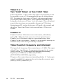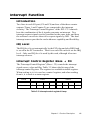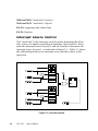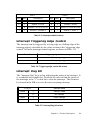
1
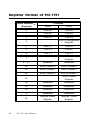
PCI-1751 48-bit Digital Input/ Output Card for PCI Bus Users Manual Copyright This documentation and the software included with this product are copyrighted 1998 by Advantech Co., Ltd. All rights are reserved. Advantech Co., Ltd. reserves the right to make improvements in the products described in this manual at any time without notice. No part of this manual may be reproduced, copied, translated or transmitted in any form or by any means without the prior written permission of Advantech Co., Ltd. Information provided in this manual is intended to be accurate and reliable. However, Advantech Co., Ltd. assumes no responsibility for its use, nor for any infringements of the rights of third parties which may result from its use. Acknowledgments PC-LabCard is a trademark of Advantech Co., Ltd. IBM and PC are trademarks of International Business Machines Corporation. MS-DOS and Windows are trademarks of Microsoft Corporation. Intel and Pentium are trademarks of Intel Corporation. CE notification The PCI-1751, developed by ADVANTECH CO., LTD., has passed the CE test for environmental specifications when shielded cables are used for external wiring. We recommend the use of shielded cables. This kind of cable is available from Advantech. Please contact your local supplier for ordering information. Part No. 2003175100 1st Edition Printed in Taiwan August 1998 Contents Chapter 1 General Information ............................. 1 Introduction .......................................................................... 2 Chapter 2 Installation .............................................. 5 Initial Inspection .................................................................. 6 Unpacking ............................................................................ 6 Jumper Settings ................................................................... 7 PCI-1751 Block Diagram .................................................. 10 Pin Assignments ................................................................. 11 Installation Instructions ..................................................... 12 Chapter 3 Operation .............................................. 13 Operation ........................................................................... 14 Digital I/O Ports ................................................................. 14 Timer/Counter Operation .................................................. 17 Interrupt Function .............................................................. 19 Appendix A Function of 8254 Counter Chip ...... 23 Appendix B Register Format of PCI-1751 ......... 31 CHAPTER 1 General Information Chapter 1 General Information 1 Introduction The PCI-1751 is a 48-bit DI/O and counter/timer card with PCI bus. It provides you with 48 bits of parallel digital input/output as well as 3 timers. It emulates mode 0 of the 8255 PPI chip, but the buffered circuits offer a higher driving capability than the 8255. The card emulates two 8255 PPI chips to provide 48 DI/O bits. The I/O bits are divided into six 8-bit I/O ports: A0, B0, C0, A1, B1 and C1. You can configure each port as either input or output via software. The dual interrupt handling capability provides users the flexibility to generate interrupts to a PC. A pin in the connector can output a digital signal simultaneously with the card's generating an interrupt. This card uses a high density SCSI 68-pin connector for easy and reliable connections to field devices. Two other features give the PCI-1751 practical advantages in an industrial setting. When the system is hot reset (the power is not turned off) the PCI-1751 retains the last I/O port settings and output values if the user has set jumper JP4 to enable this feature. Otherwise, port settings and output values reset to their safe default state, or to the state determined by other jumper settings. The PCI-1751's other useful feature is it supports both wet and dry contacts, allowing it to interface with other devices more easily. Numbering Convention All numbers given in this manual are in decimal format unless specifically noted otherwise. In particular, where a register address is given as (Base + 32), the decimal number "32" should be added to the base value. Features • 48 TTL level digital I/O lines. • Emulates mode 0 of 8255 PPI • Buffered circuits provide higher driving capability 2 PCI-1751 User's Manual • Interrupt handling • Interrupt output pin for simultaneously triggering external devices with the interrupt • High density SCSI 68-pin connector • Output status readback • Two 16-bit timers can be cascaded to one 32-bit timer, and can generate watchdog timer interrupts • One 16-bit event counter can generate event interrupts • Keeps port I/O settings and digital output states after hot system reset • Supports dry contact and wet contact Applications • Industrial AC/DC I/O devices monitoring and control • Relay and switch monitoring and control • Parallel data transfer • Sensing the signals of TTL, DTL, CMOS logic • Driving indicator LEDs Specifications I/O channels: 48 digital I/O lines Programming mode: 8255 PPI mode 0 Input Signal • Logic high voltage: 2.0 to 5.25 V • Logic low voltage: 0.0 to 0.80 V • High level input current: 20 µA • Low level input current: -0.2 mA Chapter 1 General Information 3 Output Signal • Logic high voltage: 2.4 V minimum. • Logic low voltage: 0.4 V maximum • High level input current: 15 mA maximum (source) • Low level input current: 24 mA maximum (sink) • Driving capability: 15 LS TTL Interrupt Source • PC00, PC04, PC10, PC14, Timer 1 and Counter 2. Transfer Rate (This value depends on software and speed of computer.) • Typical: 1 MB/sec (tested under DOS, Pentium® 100 MHz CPU) • Maximum: 1.5 MB/sec Connector: One SCSI-II 68-pin female connector Power consumption: 5 V @ 850 mA (Typical) 5 V @ 1.0 A (Max.) Operating temperature: 0 ~ 70º C (32º F ~ 158 ºF) Storage temperature: -20 ~ 80º C(-4º F ~ 176º F) Humidity: 5% ~ 95% non-condensing Dimension: 170 x 100 mm (6.9" x 3.9") 4 PCI-1751 User's Manual CHAPTER Installation 2 Chapter 2 Installation 5 Initial Inspection Before starting to install the PCI-1751, make sure there is no visible damage on the card. We carefully inspected the card both mechanically and electrically before shipment. It should be free of marks and in perfect order on receipt. As you unpack the PCI-1751, check it for signs of shipping damage (damaged box, scratches, dents, etc.) If it is damaged or fails to meet its specifications, notify our service department or your local sales representative immediately. Also, call the carrier immediately and retain the shipping carton and packing materials for inspection by the carrier. We will then make arrangements to repair or replace the unit. Unpacking The PCI-1751 contains components that are sensitive and vulnerable to static electricity. Discharge any static electricity on your body to ground by touching the back of the system unit (grounded metal) before you touch the board. Remove the PCI-1751 card from its protective packaging by grasping the card's rear panel. Handle the card only by its edges to avoid static discharge which could damage its integrated circuits. Keep the antistatic package. Whenever you remove the card from the PC, please store the card in this package for its protection. You should also avoid contact with materials that hold static electricity such as plastic, vinyl and styrofoam. Check the product contents inside the packing. There should be one card, one CD-ROM, and this manual. Make sure nothing is missing. 6 PCI-1751 User's Manual Jumper Settings We designed the PCI-1751 with ease-of-use in mind. It is a "plug and play" card, i.e. the system BIOS assigns the system resources such as base address and interrupt automatically. There are only two functions with 11 jumpers to be set by the user. The following section describes how to configure the card. You may want to refer to the figure below for help in identifying card components. Figure 2-1: Location of connectors and jumpers Jumper Settings to Set Ports as Input or Output by Software By shorting the upper two pins of jumpers JPA0, JPB0, JPC0L, JPC0H, JPA1, JPB1, JPC1L or JPC1H, a user sets the corresponding ports to be configurable as input or output ports by software. (JPA0 means jumper for port A0, JPB0 means jumper for port B0, etc.) The initial state of each port after system power on or reset will be set as input logic 1 (voltage high), provided that no external signals are connected, and provided jumper JP4 does not determine otherwise (see Jumper J4 discussion below). Chapter 2 Installation 7 Using Jumpers to Set Ports as Output Ports By shorting the lower two pins of the jumpers JPA0, JPB0, JPC0L, JPC0H, JPA1, JPB1, JPC1L or JPC1H, a user sets the corresponding ports to be output ports. (JPA0 means jumper for port A0, JPB0 means jumper for port B0, etc.) Shorting the lower two pins of a port's jumper pins disables the port from being software configurable as an input port. The initial state of each of these ports after system power on or reset will be logic 0 (voltage low), unless jumper JP4 determines otherwise. (See Jumper JP4 below.) Jumper JP4 Restores Ports to Their Condition Prior to Reset Jumper JP4 gives the PCI-1751 a new and valuable capability. With JP4 enabled, the PCI-1751 "memorizes" all port I/O settings and output values, and, in the event of a "hot" reset, the settings and output values present at the port just prior to reset are restored to each port following reset. This feature applies to both ports set by software, and to ports configured as output ports via jumper. Depending on the application, this capability may allow a card to be reset without requiring a complete shutdown of processes controlled by the card (since port values are left unchanged and are interrupted only momentarily). Complete loss of power to the chip clears chip memory. Thus, even if JP4 is enabled, if the power to the card is disconnected, the card's initial power-on state will be the default state (for software-set ports) or the state of an output port with voltage low output (for jumper-set ports). When jumper JP4 is not enabled, power-off or reset results in ports returning to their default state (for software-set ports) or returning to the state of output port with voltage low output (for jumper-set ports). 8 PCI-1751 User's Manual Select Clock Source of Timers and Counter Jumpers JP1, JP2 and JP3 are used to select the clock source of Timer 0, Timer 1 and Counter 2, respectively. Short the upper two pins of the jumpers to select an external clock source, or short the lower two pins to select an internal clock source. However, the internal clock source of Timer 1 is connected to the output of Timer 0, so shorting the upper two pins of JP2 results in the cascading of Timer 0 and Timer 1 as a 32-bit timer. N am es o f J u m p er s JPA0, JPA1: Jumpers for ports A0, A1 F u n c t i o n d es c r i p t i o n 1 Sets port as an output port JPB0, JPB1: Jumpers for ports B0, B1 JPC0L, JPC1L: Jumpers for low nibble of ports C0, C1 1 Sets port to be software configurable as input or output (default) 1 Internal counter clock source 1 External counter clock source (default) JPC0H, JPC1H: Jumpers for high nibble of ports C0, C1 JP1: Timer 0 JP2: Timer 1 JP3: Counter 2 1 JP 4 1 All ports return to state held just prior to reset All ports return to default states (for software-set ports) or to output port, output low (for jumper-set ports) Table 2-1: Summary of jumper settings Chapter 2 Installation 9 PCI-1751 Block Diagram Timer 0 Timer 1 Figure 2-2: PCI-1751 block diagram 10 PCI-1751 User's Manual Pin Assignments Description of pin use: PA00 ~ PA07: I/O pins of Port A0 PA10 ~ PA17: I/O pins of Port A1 PB00 ~ PB07: I/O pins of Port B0 PB10 ~ PB17: I/O pins of Port B1 PC00 ~ PC07: I/O pins of Port C0 PC10 ~ PC17: I/O pins of Port C1 CNT0_OUT, CNT1_OUT and CNT2_OUT: Output pins of Counter/Timer 0, 1 and 2 CNT0_CLK, CNT1_CLK and CNT2_CLK: External clock source of Counter / Timer 0, 1 and 2 CNT0_G, CNT1_G and CNT2_G: Gate control pins of Counter / Timer 0, 1 and 2 PA00 PA01 PA02 PA03 PA04 PA05 PA06 PA07 GND PB00 PB01 PB02 PB03 PB04 PB05 PB06 PB07 GND PC00 PC01 PC02 PC03 PC04 PC05 PC06 PC07 GND CNT0_OUT GND CNT1_OUT GND CNT2_OUT INT_OUT VCC 1 2 3 4 5 6 7 8 9 10 11 12 13 14 15 16 17 18 19 20 21 22 23 24 25 26 27 28 29 30 31 32 33 34 35 36 37 38 39 40 41 42 43 44 45 46 47 48 49 50 51 52 53 54 55 56 57 58 59 60 61 62 63 64 65 66 67 68 PA10 PA11 PA12 PA13 PA14 PA15 PA16 PA17 GND PB10 PB11 PB12 PB13 PB14 PB15 PB16 PB17 GND PC10 PC11 PC12 PC13 PC14 PC15 PC16 PC17 GND CNT0_CLK CNT0_G CNT1_CLK CNT1_G CNT2_CLK CNT2_G VCC INT_OUT: Interrupt output. This pin changes to logic 1 whenever the PCI-1751 generates an interrupt, and returns to logic 0 when the interrupt is cleared. GND: Ground VCC: +5 VDC voltage output Chapter 2 Installation 11 Installation Instructions The PCI-1751 can be installed in any PCI slot in the computer. However, refer to the computer user's manual to avoid any mistakes and danger before you follow the installation procedure below: 1. Turn off your computer and any accessories connected to the computer. Warning! TURN OFF your computer power supply whenever you install or remove any card, or connect and disconnect cables. 2. Disconnect the power cord and any other cables from the back of the computer. 3. Remove the cover of the computer. 4. Select an empty 5 V PCI slot. Remove the screw that secures the expansion slot cover to the system unit. Save the screw to secure the interface card retaining bracket. 5. Carefully grasp the upper edge of the PCI-1751. Align the hole in the retaining bracket with the hole on the expansion slot and align the gold striped edge connector with the expansion slot socket. Press the card into the socket gently but firmly. Make sure the card fits the slot tightly. 6. Secure the PCI-1751 by screwing the mounting bracket to the back panel of computer. 7. Attach any accessories (68-pin cable, wiring terminal, etc.) to the card. 8. Replace the cover of your computer. Connect the cables you removed in step 2. 9. Turn the computer power on. 12 PCI-1751 User's Manual CHAPTER 3 Operation Chapter 3 Function Description 13 Operation This chapter describes the operating characteristics of the PCI-1751. The driver software provided allows a user to access all of the card's functions without register level programming. Please see the User's Manual for the driver bundled with this card for more information. For users who prefer to implement their own bit-level programming to drive the card's functions, information useful for making such a program is included in this chapter. Digital I/O Ports Introduction The PCI-1751 emulates two 8255 programmable peripheral interface (PPI) chips in mode 0, but with higher driving capability than a standard 8255 chip. Each of the 8255 chips has 24 programmable I/O pins that are divided into three 8-bit ports. The total 48 DI/O pins from both chips are divided into 6 ports, designated PA0, PB0, PC0, PA1, PB1 and PC1. Each port can be programmed as an input or an output port. The I/O pins in port A0 are designated PA00, PA01,..., PA07; the pins in port B0 are designated PB00, PB01,..., PB07, etc. These port names are used both in this manual and in the software library. Refer to Section 2.5, Pin Assignments. 8255 Mode 0 The basic functions of 8255 mode 0 include: • Two 8-bit I/O ports - port A (PA) and port B (PB) • Port C is divided into two nibble-wide (4-bit) I/O ports:- PC upper and PC lower • Any port can be used for either input or output. • Output status can be read back. 14 PCI-1751 User's Manual Interrupt Function of the DIO Signals Two I/O pins (PC00 and PC10) can be used to generate hardware interrupts. A user can program the interrupt control register (Base + 32) to select the interrupt sources. Refer to "Interrupt Function" in this chapter for details about interrupt control. Input/Output Control A control word can be written to a port's configuration register (Base+3 for port 0 and Base+7 for port 1) to set the port as an input or an output port, unless the ports are set as output ports via jumpers (refer to Section 2.3, Jumper Settings). Table 3-1 shows the format of a control word. D7 D6 D5 D4 D3 D2 Don't care Don't care Don't care PortA Port C Don't 0: output higher care 1: input bits 0: output 1: input D1 D0 Port B Port C 0: output lower 1: input bits 0: output 1: input Table 3-1: Bit map of port configuration register Note: A control word has no effect if the corresponding port is set as an output port by a jumper. Warning! Before setting any port as an output port via software, make sure that a safe output value has also been set. An output voltage will appear at the pins immediately following the control word taking effect. If no output value was specified, the value will be indeterminate (either 0 or 1), which may cause a dangerous condition. Chapter 3 Function Description 15 Initial Configuration The initial configuration of each port depends on the input/output jumper setting of each port, on the setting of the jumper JP4, and on whether the power was actually disconnected or whether the system was hot reset. If jumper JP4 is not enabled, all ports configured by software are automatically set as input ports during system start up or reset, with a default signal level of logic 1 (high). All ports set via jumpers as output ports are set as output ports during system start up or reset, signal level logic 0 (0 V). If the jumper JP4 is enabled and the initial configuration is caused by a reset, all ports will return to the states they had just prior to the reset. The reset must be a "hot" reset (power not disconnected) for enabled JP4 to return ports to their prior values. Otherwise, the card behaves as though JP4 were not enabled. Refer to "Jumper settings" in Chapter 2 for more information. Dry Contact Support for Digital Input Each digital input channel accepts either dry contact or 0 ~ 5 VDC wet contact inputs. Dry contact capability allows the channel to respond to changes in external circuitry (e.g., the closing of a switch in the external circuitry) when no voltage is present in the external circuit. Figure 3-1 shows external circuitry with both wet and dry contact components, connected as an input source to one of the card's digital input channels. External Internal PC 5V 10 K Ω Buffer 1.5 K Ω 0.5 W Dry Contact: Open High Close Low Wet Contact: 2.0~5.25 V D C High 0~0.8 V D C Low Resistor in Parallel Figure 3-1: Wet and dry contact inputs 16 PCI-1751 User's Manual Note: For wet contact configurations, a malfunction may occur if the internal resistance of the voltage source is significant (> 1.5 kΩ). It is advisable to connect a 1.5 kΩ resistor in parallel with such a voltage source to avoid a voltage rise inside the voltage source. Timer/Counter Operation Introduction The PCI-1751 includes one 8254 compatible programmable timer/ counter chip which provides three 16-bit counters, designated as Timer 0, Timer1 and Counter 2. Each has 6 operation modes. Timer 0 and Timer 1 can be used separately or can be cascaded to create one 32-bit timer. Both Timer 1 and Counter 2 can generate interrupts to the computer. Please refer to Appendix A for more information on the operation modes of the counter chip. The block diagram of the timer/ counter system is shown in Figure 3-2. Figure 3-2: Timer and counter structure Chapter 3 Function Description 17 Timer 0 & 1: Two 16-bit Timers or One 32-bit Timer Timer 0 and Timer 1 of the counter chip can be used separately or can be cascaded to create a 32-bit programmable timer by setting jumper JP2. By setting the clock source of Timer 1 to be an external source, you can user Timer 0 and Timer 1 as two separate 16-bit timers. By setting the clock source of Timer 1 to be the output of Timer 0 (internal source) these two timers are cascaded to become one 32-bit timer. Setting jumper JP1 sets the clock source of Timer 0 to be external, and this allows Timer 0 and Timer 1 to be cascaded into a 32-bit event counter. Counter 2 Counter 2 can be a 16-bit timer or an event counter, selectable by setting JP3. When the clock source is set for an internal source, Counter 2 is a 16-bit timer; when set as an external source, then Counter 2 is an event counter. Counter 2 is set as mode 0 (interrupt on terminal count) in the driver provided by Advantech. Timer/Counter Frequency and Interrupt The input clock frequency of the counter/timers is 10 MHz. The output of both Timer 1 and Counter 2 can generate interrupts for the system (refer to section 3.3). The maximum and minimum timer interrupt frequency is (10 MHz)/(2)=(5 MHz) and (10 MHz)/ (65535*65535)=0.002328 Hz, respectively. The gates of the counter/timers are internally pulled to +5 V when gate control is enabled, but a user can also set it using the connector pins (CNT0_G, CNT1_G and CNT2_G). 18 PCI-1751 User's Manual Interrupt Function Introduction Two lines in each I/O port (C0 and C4) and two of the three counter outputs (Timer 1 and Counter 2) are connected to the interrupt circuitry. The "Interrupt Control Register" of the PCI-1751 controls how the combination of the 6 signals generates an interrupt. Two interrupt request signals can be generated at the same time, and then the software can service these two request signals by ISR. The dual interrupt sources provide the card with more capability and flexibility. IRQ Level The IRQ level is set automatically by the PCI plug and play BIOS and is saved in the PCI controller. There is no need for users to set the IRQ level. Only one IRQ level is used by this card, although it has two interrupt sources. Interrupt Control Register (Base + 32) The "Interrupt Control Register" (Base + 32) controls the interrupt signal source, edge and flag. Table 3-2 shows the bit map of the interrupt control register. The register is a readable/writable register. When writing to it, it is used as a control register, and when reading from it, it is used as a status register. Port # Port 1 Port 0 Bit # D7 D6 D5 D4 D3 D2 D1 D0 Abbreviation F1 E1 M11 M10 F0 E0 M01 M00 Table 3-2: Interrupt control register bit map Chapter 3 Function Description 19 M00 and M01: "mode bits" of port 0 M10 and M11: "mode bits" of port 1 E0, E1: triggering edge control bits F0, F1: flag bits Interrupt Source Control The "mode bits" in the interrupt control register determine the allowable sources of signals generating an interrupt. Bit 0 and bit 1 determine the interrupt source for port 0, and bit 4 and bit 5 determine the interrupt source for port 1, as indicated in Figure 3-3. Table 3-3 shows the relationship between an interrupt source and the values in the mode bits. Figure 3-3: Interrupt sources 20 PCI-1751 User's Manual Port 1 Port 0 M11 M10 Description M01 M00 Description 0 0 Disable interrupt 0 0 Disable interrupt 0 1 Source = PC10 0 1 Source = PC00 1 0 Source = PC10 & PC14 1 0 Source = PC00 & PC04 1 1 Source = Counter 2 1 1 Source = Timer 1 Table 3-3: Interrupt mode bit values Interrupt Triggering Edge Control The interrupt can be triggered by a rising edge or a falling edge of the interrupt signal, selectable by the value written in the "triggering edge control" bit in the interrupt control register, as shown in Table 3-4. E0 or E1 Triggering edge of interrupt signal 1 Rising edge trigger 0 Falling edge trigger Table 3-4: Triggering edge control bit values Interrupt Flag Bit The "interrupt flag" bit is a flag indicating the status of an interrupt. It is a readable and writable bit. Read the bit value to find the status of the interrupt, write "1" to this bit to clear the interrupt. This bit must be cleared in the ISR to service the next incoming interrupt. F0 & F1 Read Write Interrupt status 1 Interrupt exists 0 No interrupt 1 Clear interrupt 0 Don't care Table 3-5: Interrupt flag bit values Chapter 3 Function Description 21 22 PCI-1751 User's Manual APPENDIX A Function of 8254 Counter Chip Appendix A Function of 8254 counter Chip 23 The Intel 8254 The PCI-1751 uses the Intel 8254 compatible programmable interval timer/counter. The popular 8254 offers three independent 16-bit down counters. Each counter has a clock input, control gate and an output. You can program each counter for maximum count values from 2 to 65535. The 8254 has a maximum input clock frequency of 10 MHz. The PCI-1751 provides 10 MHz input frequencies to the counter chip from an on-board crystal oscillator. On the PCI-1751, the 8254 chip's Timer 0 and Timer 1 can be used separately or can be cascaded to create a 32-bit programmable timer by setting JP2. When the clock source of Timer 1 is from an external source, you can user Timer 0 and Timer 1 as two independent 16-bit timers. When the clock source of Timer 1 is set to be the output of Timer 0 (internal source) the two timers are cascaded as a 32-bit timer. When the clock source of Timer 0 is provided externally by setting JP1, Timers 0 and 1 can be used as a 32-bit event counter. Refer to section 2.3.3 for details of jumper settings. Counter Read/Write and Control Registers The 8254 programmable interval timer uses four registers at addresses BASE+24, BASE+25, BASE+26 and BASE+27 for read, write and control of counter functions. Register functions appear below: Register BASE+24 Function Counter 0 read/write BASE+25 Counter 1 read/write BASE+26 Counter 2 read/write BASE+27 Counter control word Since the 8254 counter uses a 16-bit structure, each section of read/ write data is split into a least significant byte (LSB) and most significant byte (MSB). To avoid errors it is important that you make read/ write operations in pairs and keep track of the byte order. 24 PCI-1751 User's Manual The data format for the control register appears below: BASE+27 8254 control, standard mode Bit D7 D6 D5 D4 D3 D2 D1 D0 Value SC1 SC0 RW1 RW0 M2 M1 M0 BCD Description: SC1 & SC0 Select counter Counter 0 SC1 0 SC0 0 1 0 1 2 1 0 Read-back command 1 1 RW1 & RW0 Select read/write operation Operation Counter latch RW1 0 RW0 0 Read/write LSB 0 1 Read/write MSB 1 0 Read/write LSB first, then MSB 1 1 M2, M1 & M0 Select operating mode M2 0 M1 0 M0 0 Mode 0 programmable one shot 0 0 1 1 programmable one shot X 1 0 2 Rate generator X 1 1 3 Square wave rate generator 1 0 0 4 Software triggered strobe 1 0 1 5 Hardware triggered strobe Appendix A Function of 8254 counter Chip 25 BCD Select binary or BCD counting BCD 0 Type Binary counting 16-bits 1 Binary coded decimal (BCD) counting If you set the module for binary counting, the count can be any number from 0 up to 65535. If you set it for BCD (Binary Coded Decimal) counting, the count can be any number from 0 to 9999. If you set both SC1 and SC0 bits to 1, the counter control register is in read-back command mode. The control register data format then becomes: BASE+27 8254 control, read-back mode Bit D7 D6 D5 D4 D3 D2 D1 D0 Value C1 C0 X 1 1 CNT STA C2 CNT = 0 Latch count of selected counter(s). STA = 0 Latch status of selected counter(s). C2, C1 & C0 Select counter for a read-back operation. C2 = 1 select Counter 2 C1 = 1 select Counter 1 C0 = 1 select Counter 0 If you set both SC1 and SC0 to 1 and STA to 0, the register selected by C2 to C0 contains a byte which shows the status of the counter. The data format of the counter read/write register then becomes: BASE+24/25/26 Status read-back mode 26 Bit D7 D6 D5 D4 D3 D2 D1 D0 Value OUT NC RW1 RW0 M2 M1 M0 BCD OUT Current state of counter output NC Null count is 1 when the last count written to the counter register has been loaded into the counting element PCI-1751 User's Manual Counter Operating Modes MODE 0 Stop on Terminal Count The output will be initially low after you set this mode of operation. After you load the count into the selected count register, the output will remain low and the counter will count. When the counter reaches the terminal count, its output will go high and remain high until you reload it with the mode or a new count value. The counter continues to decrement after it reaches the terminal count. Rewriting a counter register during counting has the following results: 1. Writing to the first byte stops the current counting. 2. Writing to the second byte starts the new count. MODE 1 Programmable One-shot The output is initially high. The output will go low on the count following the rising edge of the gate input. It will then go high on the terminal count. If you load a new count value while the output is low, the new value will not affect the duration of the one-shot pulse until the succeeding trigger. You can read the current count at any time without affecting the one-shot pulse. The one-shot is retriggerable, thus the output will remain low for the full count after any rising edge at the gate input. MODE 2 Rate Generator The output will be low for one period of the input clock. The period from one output pulse to the next equals the number of input counts in the counter register. If you reload the counter register between output pulses, the present period will not be affected, but the subsequent period will reflect the value. The gate input, when low, will force the output high. When the gate input goes high, the counter will start from the initial count. You can thus use the gate input to synchronize the counter. With this mode the output will remain high until you load the count register is loaded. You can also synchronize the output by software. Appendix A Function of 8254 counter Chip 27 MODE 3 Square Wave Generator This mode is similar to Mode 2, except that the output will remain high until one half of the count has been completed (for even numbers), and will go low for the other half of the count. This is accomplished by decreasing the counter by two on the falling edge of each clock pulse. When the counter reaches the terminal count, the state of the output is changed, the counter is reloaded with the full count and the whole process is repeated. If the count is odd and the output is high, the first clock pulse (after the count is loaded ) decrements the count by 1. Subsequent clock pulses decrement the count by 2. After time-out, the output goes low and the full count is reloaded. The first clock pulse (following the reload) decrements the counter by 3. Subsequent clock pulses decrement the count by two until time-out, then the whole process is repeated. In this way, if the count is odd, the output will be high for (N+1)/2 counts and low for (N-1)/2 counts. MODE 4 Software Triggered Strobe After the mode is set, the output will be high. When the count is loaded, the counter will begin counting. On terminal count, the output will go low for one input clock period then go high again. If you reload the count register during counting, the new count will be loaded on the next CLK pulse. The count will be inhibited while the GATE input is low. MODE 5 Hardware Triggered Strobe The counter will start counting after the rising edge of the trigger input and will go low for one clock period when the terminal count is reached. The counter is retriggerable. 28 PCI-1751 User's Manual Counter Operations Read/Write Operation Before you write the initial count to each counter, you must first specify the read/write operation type, operating mode and counter type in the control byte and write the control byte to the control register (BASE+27). Since the control byte register and all three counter read/write registers have separate addresses and each control byte specifies the counter it applies to (by SC1 and SC0), no instructions on the operating sequence are required. Any programming sequence following the 8254 convention is acceptable. There are three types of counter operation: read/load LSB, read /load MSB and read /load LSB followed by MSB. It is important that you make your read/write operations in pairs and keep track of the byte order. Counter Read-back Command The 8254 counter read-back command lets you check the count value, programmed mode and current states of the OUT pin and Null Count flag of the selected counter(s). You write this command to the control word register. The format is as shown at the beginning of this section. The read-back command can latch multiple counter output latches. Simply set the CNT bit to 0 and select the desired counter(s). This single command is functionally equivalent to multiple counter latch commands, one for each counter latched. The read-back command can also latch status information for selected counter(s) by setting STA bit = 0. The status must be latched to be read; the status of a counter is accessed by a read from that counter. The counter status format appears at the beginning of the chapter. Appendix A Function of 8254 counter Chip 29 Counter Latch Operation Users often want to read the value of a counter without disturbing the count in progress. You do this by latching the count value for the specific counter then reading the value. The 8254 supports the counter latch operation in two ways. The first way is to set bits RW1 and RW0 to 0. This latches the count of the selected counter in a 16-bit hold register. The second way is to perform a latch operation under the read-back command. Set bits SC1 and SC0 to 1 and CNT = 0. The second method has the advantage of operating several counters at the same time. A subsequent read operation on the selected counter will retrieve the latched value. Counter Applications The 8254 compatible programmable interval timer/counter on your PCI-1751 interface card is a a very useful device. You can program timers 1 and 2 to serve as timers, event counters, square wave generators, or as a watchdog to generate regular interrupts at a fixed interval. 30 PCI-1751 User's Manual APPENDIX B Register Format of PCI-1751 Appendix A Function of 8254 counter Chip 31 Register Format of PCI-1751 Base Address (Decimal) + Function Read Write 0 Port A0 Port A0 1 Port B0 Port B0 2 Port C0 Port C0 Port 0 Configuration Register 3 4 Port A1 Port A1 5 Port B1 Port B1 6 Port C1 Port C1 Port 1 Configuration Register 7 8 ~ 23 Reserved Reserved 24 8254 Counter 0 8254 Counter 0 25 8254 Counter 1 8254 Counter 1 26 8254 Counter 2 8254 Counter 2 8254 Control Register 27 32 28 Reserved Reserved 29 Reserved Reserved 30 Reserved Reserved 31 Reserved Reserved 32 Interrupt Status Register Interrupt Control Register PCI-1751 User's Manual