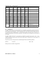
1
MMT-188EB
80C188EB Microprocessor Board
Rev H
HARDWARE / SOFTWARE
USER'S REFERENCE MANUAL
(c) 1999
MIDWEST MICRO-TEK
The information in this manual is subject to change without notice. Midwest Micro-Tek makes no
warranty of any kind with regard to this manual, including, but not limited to, any implied warranties of
merchantability and fitness for a particular purpose. Midwest Micro-Tek makes no commitment to
update, nor to keep current the information contained in this manual.
Midwest Micro-Tek
1010 32nd Avenue
Brookings, SD 57006
Ph. (605) 697-8521
Fax (605) 692-5112
E Mail: [email protected]
URL: www.midwestmicro-tek.com
PREFACE
User Feedback
At Midwest Micro-Tek we are always interested in user comments and suggestions. We would like to
know how well you like our products. We also like to know if you feel there is something missing either
in terms of features offered, or in our documentation. We value your ideas and information!
Customization
Midwest Micro-Tek will modify hardware and software to customer specifications with a minimum
quantity purchase, or on a consulting basis.
PRIOR TO INSTALLATION
!
Set the necessary jumpers on the MMT-188EB board for the memory and I/O configuration
intended. See Section 2-5, Memory Configuration on pages 9-11.
!
Verify that the terminal cable you are using is correct as specified in Appendix B of this manual.
It may be necessary to jumper the CTS (clear to send) signal on the board for communication
with your terminal device. The MMT-188EB is configured as a DCE device and may require a
NULL modem connector to communicate with older PC's. Please check your PC specifications
for RS-232 compatibility.
!
Midwest Micro-Tek cannot assume responsibility for problems caused by improper power supply
connections.
!
Before operating the MMT-188EB embedded controller, please verify that the +5 volt power
supply is plugged into a wall socket, and the power lead is connected to the controller's power
jack
MMT-188EB User's Manual
ii
PREFACE
Supplemental Materials
This manual provides general information, installation instructions, programming specifications,
principles of operation, and service information for the MMT-188EB microcomputer board.
Supplemental information may be found in the data sheets included on the CD-ROM. The following data
sheets are included on the CD-ROM:
!
80C188EB.PDF
Intel 80C186EB / 80C188EB User's Manual
!
82C55.PDF
Programmable Peripheral Interface
!
MAX690A.PDF
Maxim Microprocessor Supervisory Circuit
!
DS1315.PDF
Dallas Semiconductor Phantom Time Chip
!
24LC16B.PDF
16K Serial EEPROM
!
AM29F016.PDF
AMD 2MB Flash Memory
!
MAX197.PDF
Maxim 12-Bit D/A Converter
!
MAX527.PDF
Maxim 12-Bit A/D Converter
The above references give excellent information for the complete utilization of the MMT-188EB
microcomputer board. It is beyond the scope of this document to instruct the user in assembly language,
or higher level language programming.
User Assistance
If the information you need for configuring this board is not present in this document, please do not
hesitate to call us for technical support. At Midwest Micro-Tek, we want to make the use of this board as
pleasant and trouble free as possible.
MMT-188EB User's Manual
iii
PREFACE
CHAPTER ONE - Specifications
1-1
Introduction . . . . . . . . . . . . . . . . . . . . . . . . . . . . . . . . . . . . . . . . . . . . . . . . . . . . . . . . . . .
Manual Notation . . . . . . . . . . . . . . . . . . . . . . . . . . . . . . . . . . . . . . . . . . . . . . . . . . . . . . .
1-2
General Description . . . . . . . . . . . . . . . . . . . . . . . . . . . . . . . . . . . . . . . . . . . . . . . . . . . . .
Standard Features . . . . . . . . . . . . . . . . . . . . . . . . . . . . . . . . . . . . . . . . . . . . . . . . . . . . . . .
Options . . . . . . . . . . . . . . . . . . . . . . . . . . . . . . . . . . . . . . . . . . . . . . . . . . . . . . . . . . . . . . .
1-3
Equipment Supplied . . . . . . . . . . . . . . . . . . . . . . . . . . . . . . . . . . . . . . . . . . . . . . . . . . . . .
1-4
Equipment Required . . . . . . . . . . . . . . . . . . . . . . . . . . . . . . . . . . . . . . . . . . . . . . . . . . . .
1-5
Specifications . . . . . . . . . . . . . . . . . . . . . . . . . . . . . . . . . . . . . . . . . . . . . . . . . . . . . . . . . .
Standard Features . . . . . . . . . . . . . . . . . . . . . . . . . . . . . . . . . . . . . . . . . . . . . . . . . . . . . . .
Options . . . . . . . . . . . . . . . . . . . . . . . . . . . . . . . . . . . . . . . . . . . . . . . . . . . . . . . . . . . . . . .
1
1
1
1
1
2
2
2
2
3
CHAPTER TWO - Getting Started
2-1
Installation Considerations . . . . . . . . . . . . . . . . . . . . . . . . . . . . . . . . . . . . . . . . . . . . . . . 4
2-2
Static Electricity (ESD) Considerations . . . . . . . . . . . . . . . . . . . . . . . . . . . . . . . . . . . . . 4
2-3
Jumper Installation . . . . . . . . . . . . . . . . . . . . . . . . . . . . . . . . . . . . . . . . . . . . . . . . . . . . . . 4
2-4
Serial I/O . . . . . . . . . . . . . . . . . . . . . . . . . . . . . . . . . . . . . . . . . . . . . . . . . . . . . . . . . . . . . 5
RTS and CTS Considerations . . . . . . . . . . . . . . . . . . . . . . . . . . . . . . . . . . . . . . . . . . . . . 5
JP14 (Ch 0) & JP16 (Ch 1) - Description . . . . . . . . . . . . . . . . . . . . . . . . . . . . . . . . . . . . 6
RS-422/485 Operation . . . . . . . . . . . . . . . . . . . . . . . . . . . . . . . . . . . . . . . . . . . . . . . . . . . 6
Networking using RS-845 . . . . . . . . . . . . . . . . . . . . . . . . . . . . . . . . . . . . . . . . . . . . . . . . 6
Table 2-4.1: Channel 0 biasing and grounding jumper table . . . . . . . . . . . . . . . . . . . . 7
Table 2-4.2: Channel 1 biasing and grounding jumper table . . . . . . . . . . . . . . . . . . . . 7
Figure 2-4.1: RS-485 Network Schematic . . . . . . . . . . . . . . . . . . . . . . . . . . . . . . . . . . . 8
Serial Channel Interrupts . . . . . . . . . . . . . . . . . . . . . . . . . . . . . . . . . . . . . . . . . . . . . . . . . 8
2-5
Memory Configuration . . . . . . . . . . . . . . . . . . . . . . . . . . . . . . . . . . . . . . . . . . . . . . . . . . 9
Table 2-5.1 - RAM Jumpers. RAM Socket U4 . . . . . . . . . . . . . . . . . . . . . . . . . . . . . . . 9
Table 2-5.2 - ROM Jumpers. ROM Socket U3 . . . . . . . . . . . . . . . . . . . . . . . . . . . . . . . 9
Table 2-5.3 - ROM Jumpers. ROM Socket U3 (with FLASH installed) . . . . . . . . . . . 10
Table 2-5.4 - ROM Jumpers. ROM Socket U3 (with EEPROM installed) . . . . . . . . . 10
Table 2-5.5 - ROM Jumpers. ROM Socket U3 (with RAM installed) . . . . . . . . . . . . . 11
2-6
Parallel Port . . . . . . . . . . . . . . . . . . . . . . . . . . . . . . . . . . . . . . . . . . . . . . . . . . . . . . . . . . 11
2-7
Watchdog Timer/Power Fail Detector . . . . . . . . . . . . . . . . . . . . . . . . . . . . . . . . . . . . . . 12
2-8
60-Pin Expansion Header . . . . . . . . . . . . . . . . . . . . . . . . . . . . . . . . . . . . . . . . . . . . . . . 12
CHAPTER THREE - Programming Reference
3-1
82C55A Programmable Peripheral Interface - PPI (or compatible) . . . . . . . . . . . . . . .
3-2
80C188EB Chip Select Unit . . . . . . . . . . . . . . . . . . . . . . . . . . . . . . . . . . . . . . . . . . . . .
3-3
LAN Circuitry - Optional . . . . . . . . . . . . . . . . . . . . . . . . . . . . . . . . . . . . . . . . . . . . . . .
3-4
MAXIM - MAX197 - 12-bit Analog-to-Digital Converter - Optional . . . . . . . . . . . . .
3-5
MAXIM - MAX527 - 12-bit Digital-to-Analog Converter - Optional . . . . . . . . . . . . .
14
14
14
14
15
MMT-188EB User's Manual
iv
TABLE OF CONTENTS
APPENDIX A - Jumper Settings
Table A-1: Jumper Defaults and Definitions. . . . . . . . . . . . . . . . . . . . . . . . . . . . . . . . . 16
APPENDIX B - Pinouts, Port I/O, & Memory Assignments
B-1
RS-232 Pinouts . . . . . . . . . . . . . . . . . . . . . . . . . . . . . . . . . . . . . . . . . . . . . . . . . . . . . . .
Table B-1.1: RS-232 Pinout . . . . . . . . . . . . . . . . . . . . . . . . . . . . . . . . . . . . . . . . . . . . .
Figure B-1.1: RS-232 Pinouts . . . . . . . . . . . . . . . . . . . . . . . . . . . . . . . . . . . . . . . . . . . .
B-2
RS-422 Pinouts . . . . . . . . . . . . . . . . . . . . . . . . . . . . . . . . . . . . . . . . . . . . . . . . . . . . . . .
Table B-2.1: RS-422/485 Pinouts . . . . . . . . . . . . . . . . . . . . . . . . . . . . . . . . . . . . . . . . .
B-3
60-Pin Expansion Header . . . . . . . . . . . . . . . . . . . . . . . . . . . . . . . . . . . . . . . . . . . . . . .
Table B-3.1: 60 Pin Expansion Header Pinout . . . . . . . . . . . . . . . . . . . . . . . . . . . . . . .
B-4
OPTO22 Interface . . . . . . . . . . . . . . . . . . . . . . . . . . . . . . . . . . . . . . . . . . . . . . . . . . . . .
Table B-4.1: OPTO22 Standard Interface - Pinout . . . . . . . . . . . . . . . . . . . . . . . . . . . .
B-5
Port/Memory Addresses for the MMT-188EB . . . . . . . . . . . . . . . . . . . . . . . . . . . . . . .
Table B-5.1: Port/Memory Assignments . . . . . . . . . . . . . . . . . . . . . . . . . . . . . . . . . . .
MMT-188EB User's Manual
18
18
18
18
18
19
19
20
20
21
21
v
CHAPTER ONE - Specifications
1-1
Introduction
Thank you for purchasing the MMT-188EB. We hope that you find it to be reliable, flexible and easy to
use. This board is a complete microcomputer, requiring only a +5 volt power supply to operate.
This board has received a 50 hour dynamic burn-in under continuous loop diagnostics to insure a high
level of reliability for your product.
Manual Notation
Every discussion of microprocessor systems requires a method of denoting an active low signal. This
manual uses a "#" pound symbol following the label name to indicate such signals. Additionally, when
referring to bits within a byte, the 8 bits are assumed to be numbered 0 through 7 with 0 being the least
significant of these. Lastly, the designation of "HIGH" and logic level "1" is equivalent to a bit being set
and "LOW" or "0" as a bit being cleared. These are used throughout this manual. All notations used in
this manual are consistent with the notations used by major IC industry sources.
The notation used in the jumper tables in this document are as follows:
1&2
A 3-pin block with a jumper installed on pins 1 and 2
2&3
A 3-pin block with a jumper installed on pins 2 and 3
ON
A 2-pin block with a jumper installed
OUT
No jumper installed on this block
XXX
Does not matter
1-2
General Description
Standard Features
!
Intel 80C188EB CPU at 20 MHz
!
Up to 1 MB of fully addressable memory
!
2 Serial I/O ports (2 - RS-232 standard or 2-RS-422/485 optional)
!
24 bits of parallel I/O
!
2 counter/timers
!
3 Hardware Interrupt Lines
!
Watchdog timer & Power fail detector
!
60-pin header for direct access to uP and peripheral lines
!
3 Status LEDs
Options
!
8 channels of 12-bit analog to digital converter
!
4 channels of 12-bit digital to analog converter
!
Dallas Semiconductor Phantom Time Chip and nonviolatile memory controller
!
RS-485 Line Driver/Receiver for Serial Communications
!
8-Pin DIP Switch for LAN Operation
!
Monitor/Debugger EPROM and 32kx8 SRAM
!
EPROM & SRAM
!
Parallel, Serial, and Power Cabling
!
Interface for an LCD and a 4x4 keypad
!
2 MB Flash
!
ROMDOS on EPROM with a 2MB Flash Disk
1-3
Equipment Supplied
MMT-188EB User's Manual
1
CHAPTER ONE - Specifications
!
!
MMT-188EB Microcomputer Board
CD-ROM containing:
" I/O Equates
" Sample Code
" Manuals
" Datasheets
" Schematics
" Silk Screen
1-4
!
!
Equipment Required
+5 volt DC power supply - 1A minimum
Serial I/O terminal or PC with communication software (Procomm or HyperTerminal is
suggested)
1-5
Specifications
Standard Features
!
Intel 80C188EB microprocessor
" 20 MHz CPU clock rate
" Operating Temperature range: -40 EC to 85 EC
" RH: to 90% without condensation
!
Up to 1 MB of fully addressable memory in the form of
" 2 32-pin "byte-wide" memory sockets which may contain up to 2, 512kx8 bit memory units
for a possible 1 MB of memory
" Up to 512kx8 RAM / ROM / EPROM / EEPROM / 5V FLASH (32 pin socket U3)
" Up to 512kx8 SRAM (32 pin socket U4)
!
2 Serial I/O ports
" Asynchronous rates to 115K baud
" Synchronous rates to 4 Mbaud
" RS-232 interface
" RS-485 interface (optional)
Party Line or point-to-point
Communication distances up to 5000 feet
" RTS and CTS for handshaking
!
24 bits of parallel I/O
" 24 bits of parallel I/O via Intel 82C55A (or compatible)
Terminated at an OPTO22 Standard 50-pin straight header
!
2 counter/timers available to the user
!
Watchdog Timer & Power Fail Detector
MMT-188EB User's Manual
2
CHAPTER ONE - Specifications
!
60-pin header
" Access to all data and address lines
" Clock output at 1/2 the oscillator frequency
" Read and Write Lines (RD# and WR#)
" 2 timer/counters
" +5 and ground
" 3 User I/O chip selects
" Off-board memory chip selects
" Nonmaskable interrupt
" 2 Maskable interrupts
" Reset (Output)
" Ready (Input)
" Hold and Hold Acknowledge
" Battery Voltage (Input/Output)
Options
!
8 channels of 12-bit analog to digital converter
!
4 channels of 12-bit digital to analog converter
!
Dallas Semiconductor Phantom Time Chip and nonviolatile memory controller
!
RS-485 Line Driver/Receiver for Serial Communications
!
8-Pin DIP Switch for LAN Operation
!
Monitor/Debugger EPROM and 32kx8 SRAM
!
EPROM & SRAM
!
Parallel, Serial, and Power Cabling
!
2 MB Flash
!
ROMDOS on EPROM with a 2MB Flash Disk
MMT-188EB User's Manual
3
CHAPTER TWO - Getting Started
2-1
Installation Considerations
The MMT-188EB microcomputer board is designed as a stand-alone single board computer (SBC). A
Monitor/Debugger EPROM and 8kx8 SRAM are available as an option to allow the user to start
exercising the board immediately.
The MMT-188EB is shipped without memory devices installed in the 32-pin "byte wide" sockets.
However, a Monitor /Debugger EPROM and SRAM can be installed at an additional cost.
Note: It is important that the user's startup code reside in memory socket U3 due to the
characteristics of the chip select UCS#.
2-2
Static Electricity (ESD) Considerations
Memory devices are extremely sensitive to static electricity. When installing memory devices, be sure
that the power to the board is off and pin 1 of the device is properly oriented. A grounded, staticdissipating wrist strap should also be used in order to minimize possible static damage.
2-3
Jumper Installation
The MMT-188EB CPU board has been designed to be extremely flexible in allowing the user to
configure memory and I/O as needed for his/her particular product needs. A wide variety of "byte-wide"
parts may be used in memory sockets U3 and U4.
As shipped, the board has jumpers installed for the following configuration:
Jumper
JP3
JP4
JP5
JP9
JP10
JP11
JP24
JP14
JP15
JP16
JP17
Pins Jumped
2&3
1&2
1&2
2&3
2&3
1&2
1&2
1&2
2&3
1&2
2&3
Usage
32kx8 EPROM installed in location U3
32kx8 RAM installed in location U4
32kx8 EPROM installed in location U3
32kx8 RAM installed in location U4
32kx8 EPROM installed in location U3
32kx8 EPROM installed in location U3
32kx8 EPROM installed in location U3
CTS0# grounded for 'always on' reception of characters
RS-232 interface enabled
CTS1# grounded for 'always on' reception of characters
RS-232 interface enabled
Refer to silkscreen for location of memory IC's U3 and U4 and jumper blocks.
Additional detailed sections are provided describing each of these options.
Refer to Section 2-5: Memory Configuration & Appendix A - Jumper Settings.
MMT-188EB User's Manual
4
CHAPTER TWO - Getting Started
2-4
Serial I/O
The two DCE serial interfaces of the MMT-188EB board are configured as 9 pin serial interface
connectors compatible in pin numbering with the IBM PC 9 pin serial I/O connectors. Both serial
connectors are presented to the outside world via 10-pin headers, which can be transformed into DB9
socket connectors by way of ribbon cables. Please refer to Appendix B for proper pinouts of the 10-pin
stake headers.
Two electrical interface specifications have been provided by MMT on the MMT-188EB board. Both
RS-232 and RS-485 are available. RS-232 is the "standard" interface used by most computer users and
will be the interface of choice for most installations. Both serial connections can be configured as
independent RS-232 ports. Cabling distances of up to 50 feet are possible at 9600 baud, with longer
distances possible as the baud rate is decreased. RS-485 is provided as an option for both serial channels.
The 485 interface can operate reliably at up to 5000 feet. This interface can be configured to operate in a
"party line" mode with multiple "drops" along its entire length.
The jumper configuration for these modes is outlined in Appendix A. All MMT boards are shipped with
serial ports configured as RS-232 devices. Serial channel 0 is the default channel for the connection of
the host PC. Connect this channel to the PC's COM port if the MMT Monitor/Debugger is in use.
Refer to the silkscreen for location of the 10-pin stake headers and jumper blocks. J2 is channel 0 and J1
is channel 1.
RTS and CTS Considerations
Each RTSx# (x = 0-1) (Request to Send) signal is controlled by toggling a parallel I/O bit directly in the
80C188EB. The 80C188EB is equipped with 16 latched bits of parallel I/O. However, most of these bits
are multiplexed with other control signals, so they cannot be used for data transfer.
The RTSx# control signals have two basic functions. When using the RS-232 interface, RTSx# is used
as a handshaking signal to drive pin 8 of the DB9 socket connectors. During RS-485 operation, RTSx# is
used to control whether the 75176 Line Driver IC is transmitting or receiving. When RTSx# is cleared,
the 75176 receives data from the serial port. When this bit is set, the 75176 transmits data to the serial
port.
Note: When using the RS-232 or RS-485 interface, the RTS0# and RTS1# lines are not automatically
toggled. The user must output the correct word to the P2PIN register of the 80C188EB to set or reset
these signals.
The CTSx# inputs on the 80C188EB are used as handshaking signals to control the data flow on the
serial I/O channels. When CTSx# is tied directly to ground, the serial channel is in "receive always"
mode.
The CTSx# signals can be tied directly to ground (default setting) with jumpers JP14 & 16, or sent out to
the DB9 socket connections to be driven by other I/O devices.
MMT-188EB User's Manual
5
CHAPTER TWO - Getting Started
JP14 (Ch 0) & JP16 (Ch 1) - Description
The CTSx# (Clear to Send Serial Port x) if installed on pins 2&3, this jumper allows pin 7 of the DB9
socket connector to drive the CTSx line of the Serial Port x interface. On pins 1&2, the jumper forces
the serial channel into the "always on" mode.
RS-485 Operation
RS-485 interface allows the separation of the MMT-188EB and peripherals up to 5000 feet. A 75176 IC
is used to accomplish this by using a differential pair. Please note that a full duplex configuration is not
possible and the device desiring to transmit must raise the direction control line of the 75176 (RTSx
signals are used for this toggle). A Master/Slave relationship under software control is generally the
most straight forward communications scheme to implement. Optional LAN circuitry is available which
provides a method of addressing up to 256 slave MMT-188EBs.
Networking using RS-845
Various RS-485 configurations:
1. Interfacing one SBC to a PC using a serial link:
!
To use only one SBC interfaced to a PC, one needs to set up the SBC using the 75176 setup on
the far left of Figure 2-4.1. In doing so, enable the 100 ohm and both the 560 (or 1K) ohm
resistors. Next determine if both the PC and SBC are connected to a common earth ground. If
this is not the case, enable the 100 ohm resistor and add a grounding wire to your twisted pair.
The 100 ohm resistor insures that a damaging current build up between the two ports is
prevented. Refer to tables 2-4.1 and 2-4.2 for the biasing and grounding jumper settings.
2. Interfacing two SBC's together:
!
To interface two SBC's, refer to the two outer 75176 configurations on Figure 2-4.1. Configure
the first (master) board as described in Part 1 of this page and configure the second (slave) board
by enabling the 100 ohm biasing resistor. Refer to tables 2-4.1 and 2-4.2 for the biasing and
grounding jumper settings. Again, if a common ground is not present, enable the grounding
resistor on each board and add a grounding wire to the twisted pair.
3. Interfacing more than two SBC's:
!
When interfacing more than two SBC's, refer to the entire Figure 2-4.1. As shown, as many as
32 nodes can be added in line with the twisted pair. Note that any board that is added to the
network should not have any of the biasing resistors enabled since the master board is performing
the biasing for the entire network. The only boards that need the biasing resistors enabled is the
master (first terminal node) and the last board (final terminal node). Refer to tables 2-4.1 and 24.2 for the biasing and grounding jumper settings. If one or two or any number of the boards do
not share a common earth ground, one must enable the grounding resistor and add a grounding
wire to the twisted pair.
MMT-188EB User's Manual
6
CHAPTER TWO - Getting Started
Configuration
JP15
JP29
JP26
JP28
JP25
Master
1&2
ON
ON
ON
*
Final Node
1&2
ON
OUT
OUT
*
Additional Nodes
1&2
OUT
OUT
OUT
*
RS-232 Operation
2&3
XXX
XXX
XXX
Table 2-4.1: Channel 0 biasing and grounding jumper table
Configuration
JP17
JP27
JP30
JP31
JP37
Master
1&2
ON
ON
ON
*
Final Node
1&2
ON
OUT
OUT
*
Additional Nodes
1&2
OUT
OUT
OUT
*
RS-232 Operation
2&3
XXX
XXX
XXX
Table 2-4.2: Channel 1 biasing and grounding jumper table
*
ON
ON
This is the grounding resistor jumper. To enable it, DO NOT place a jumper on the
block. To disable it, place a shorting jumper on the block. Refer to instructions
in this section for use. (Please note that a jumper must ALWAYS be placed on this
block when in the RS-232 mode).
MMT-188EB User's Manual
7
CHAPTER TWO - Getting Started
Figure 2-4.1: RS-485 Network Schematic
Serial Channel Interrupts
Transmit and receive interrupts are available on both serial channels. Channel 0 has an interrupt vector
associated with both the receive and transmit interrupts: Type 020 and 021 respectively in the
80C188EB interrupt vector table. Serial channel 1 does not have a built in interrupt, but is connected
directly to the 80C188EB's INT1 line. This allows both channels to be operated in either the polled, or
interrupt driven modes.
MMT-188EB User's Manual
8
CHAPTER TWO - Getting Started
2-5
Memory Configuration
The "byte-wide" sockets of the MMT-188EB board have been configured to be extremely flexible. The
following list outlines the types of memory supported.
U3
8kx8, 16kx8, 32kx8, 64kx8, 128kx8, 256kx8, 512kx8 ROM devices
8kx8, 32kx8, 128kx8, 256kx8, 512kx8 RAM type devices
32kx8, 64kx8, 128kx8, 256kx8, 512kx8 5V Flash devices
8kx8, 32kx8, 128kx8, 512kx8 EEPROM type devices
U4
8kx8, 32kx8, 128kx8, 256kx8, 512kx8 RAM type devices
If you have additional "byte-wide" devices to install which are not listed above, please compare to pinout
requirements of the devices you wish to install against the possible pin configurations available through
the MMT-188EB memory jumper block. The MMT-188EB memory sockets are fully compatible with
memory devices from Benchmarq™ and Intel™ . Although most manufacturers conform to these
specifications, some do not. If you have difficulties with your SBC please verify that your memory is
properly installed and follows the specifications above.
JUMPER
8kx8
SRAM
32kx8
SRAM
128kx8
SRAM
256kx8
SRAM
512kx8
SRAM
JP4
2&3
1&2
1&2
1&2
1&2
JP9
2&3
2&3
2&3
1&2
1&2
Table 2-5.1 - RAM Jumpers. RAM Socket U4
JUMPER
8kx8
EPROM
16kx8
EPROM
32kx8
EPROM
64kx8
EPROM
128kx8
EPROM
256kx8
EPROM
512kx8
EPROM
JP3
2&3
2&3
2&3
2&3
1&2
1&2
1&2
JP5
2&3
2&3
1&2
1&2
1&2
1&2
1&2
JP6
OUT
OUT
OUT
OUT
OUT
OUT
OUT
JP7
OUT
OUT
OUT
OUT
2&3
2&3
1&2
JP8
OUT
OUT
OUT
OUT
1&2
1&2
1&2
JP10
2&3
2&3
2&3
1&2
1&2
1&2
1&2
JP11
OUT
1&2
1&2
1&2
1&2
1&2
1&2
JP12
OUT
OUT
OUT
OUT
OUT
OUT
OUT
JP13
OUT
OUT
OUT
OUT
OUT
OUT
OUT
JP24
2&3
2&3
2&3
2&3
2&3
2&3
2&3
Table 2-5.2 - ROM Jumpers. ROM Socket U3
MMT-188EB User's Manual
9
CHAPTER TWO - Getting Started
JUMPER
ATMEL
32kx8
FLASH
Other
32kx8
FLASH
64kx8
FLASH
128kx8
FLASH
256kx8
FLASH
512kx8
FLASH
JP3
2&3
1&2
1&2
1&2
1&2
1&2
JP5
1&2
1&2
1&2
1&2
1&2
1&2
JP6
2&3
OUT
OUT
OUT
OUT
OUT
JP7
OUT
OUT
OUT
OUT
OUT
OUT
JP8
OUT
2&3
2&3
2&3
2&3
2&3
JP10
OUT
1&2
1&2
1&2
1&2
1&2
JP11
1&2
1&2
1&2
1&2
1&2
1&2
JP12
OUT
OUT
OUT
OUT
OUT
OUT
JP13
OUT
2&3
2&3
2&3
2&3
2&3
JP24
2&3
2&3
2&3
2&3
2&3
2&3
Table 2-5.3 - ROM Jumpers. ROM Socket U3 (With FLASH installed)
JUMPER
8kx8
EEPROM
32kx8
EEPROM
128kx8
EEPROM
512kx8
EEPROM
JP3
2&3
2&3
1&2
1&2
JP5
OUT
OUT
1&2
1&2
JP6
OUT
1&2
OUT
OUT
JP7
OUT
OUT
OUT
OUT
JP8
OUT
OUT
OUT
1&2
JP10
OUT
OUT
1&2
1&2
JP11
OUT
1&2
1&2
1&2
JP12
ON
ON
OUT
OUT
JP13
OUT
OUT
2&3
2&3
JP24
2&3
2&3
1&2
1&2
Table 2-5.4 - ROM Jumpers. ROM Socket U3 (With EEPROM installed)
MMT-188EB User's Manual
10
CHAPTER TWO - Getting Started
JUMPER
8kx8
SRAM
32kx8
SRAM
128kx8
SRAM
256kx8
SRAM
512kx8
SRAM
JP3
2&3
2&3
2&3
1&2
1&2
JP5
OUT
OUT
OUT
OUT
OUT
JP6
OUT
1&2
1&2
1&2
1&2
JP7
OUT
OUT
OUT
OUT
OUT
JP8
OUT
OUT
OUT
OUT
1&2
JP10
OUT
OUT
OUT
OUT
OUT
JP11
2&3
1&2
1&2
1&2
1&2
JP12
ON
ON
ON
ON
ON
JP13
OUT
OUT
1&2
1&2
1&2
1&2
1&2
1&2
1&2
1&2
RAM tied to +5
2&3
2&3
2&3
2&3
2&3
RAM tied to battery backup
JP24
Table 2-5.5 - ROM Jumpers. ROM Socket U3 (with RAM installed)
2-6
Parallel Port
The MMT-188EB makes use of an Intel 82C55A (or compatible) programmable peripheral interface IC
to provide 24 lines of parallel I/O. The 82C55A divides each set of 24 lines into three ports (A, B, and
C) of eight lines each. In addition, port C is divided into two groups of four lines each. The 82C55A is
software programmable for three modes of operation. Each mode can be configured for various types of
I/O formats.
The MMT-188EB's 82C55A IC is terminated into an OPTO22 compatible 50-pin header. Note: A relay
is NOT provided to control the state of pin 49 of the OPTO header. Instead, pin 49 is used to supply +5V
to the 50-pin header.
The 82C55A resides in I/O space and is selected through GCS5# at the following address:
OPTO22
CS_8255# . . . . . . . . . . . . . . . . . . . . . . . . . . . . . .
040h - 043h
Header pinouts are available in Appendix B.
MMT-188EB User's Manual
11
CHAPTER TWO - Getting Started
2-7
Watchdog Timer/Power Fail Detector
A watchdog chip (Maxim 690) has been provided to monitor a running program and insure that the
processor has not crashed. The watchdog serves several useful functions. First, as the voltage drops
below 4.8V, the MAX690 sends out an interrupt (INT4). The interrupt allows stack, flags, and
accumulator data to be saved to the battery backed RAM before the system is halted. A program will
typically have anywhere from 50-150 ms to perform these "house cleaning" tasks before the reduced
power prevents the processor from continuing. The MAX690 will also monitor the SBC's power supply
to verify that VCC on the board is stable and above 4.8V DC. The system voltage is compared to the
supply and battery voltages. The higher of the two is gated to the SRAM VCC pins to provide constant
power to the RAM.
The MAX690 also has a watchdog timer feature. Jumper JP19 (shorted) enables the watchdog. If it is
open, the watchdog feature will be disabled. When enabled, the chip select for the 82C55A (at 040h 043h) is used as a check toggle. The watchdog input must be toggled every 1.6 seconds to insure that the
device does not reset. Any access of the 82C55A chip will therefore toggle the watchdog input.
2-8
60-Pin Expansion Header
Included on the MMT-188EB is a 60-pin expansion header for use with add-on peripheral boards. The
user has access to all 60 pins by way of a straight PCB header. The following signals are provided via
the expansion header:
!
!
!
!
!
!
20 Address Lines - (BA00 - BA19)
" Non buffered processor address lines. Do not drive more than two TTL level loads without
external buffering.
8 Data Lines - (BD00 - BD07)
" Non buffered processor data lines. Do not drive more than two TTL level loads without
external buffering.
" BD08 - BD15 are available at the bus, and are pulled high. However, they are available only
to allow compatibility with other MMT products, and are not connected the 80C188EB
processor's internal workings.
2 User Programmable Timers - (TxIN; x=0-1, TxOUT; x=0-1)
" Two counter/timers are available to the user to count events or to clock external operations.
These counter/timers are directly connected to the 80C188EB's integrated peripheral block.
The clock or counting source of both counter/timers can be either external or internal
depending on the user's application. For counting purposes input pins TxIN may be used as
clock sources.
" A third integrated timer is available to the user with only internal clocking available. The
timer uses the CPU clock to count events and has no external pins.
Clock Output (CLK)
" The CLK output pin operates at ½ the CPU's oscillator frequency
Ready Input (READY/WAIT#)
" This pin can be used to suspend CPU operation when it is driven low. The normal state of
this pin is active high due to an external pull-up resistor.
Offboard Memory Chip Select
MMT-188EB User's Manual
12
CHAPTER TWO - Getting Started
!
!
!
!
!
!
" The OBMCS# output can be used to address external memory. The memory space assigned
to this chip select is user programmable.
" On units with the 2MB of Flash (U25) installed, the Offboard Memory Chip Select will not
be available for the user.
I/O Chip Selects (IO_USER0# - 2#)
" These chip selects are driven low during I/O read and write cycles. The I/O space of these
chip selects is user programmable. Midwest Micro-Tek has placed them as follows:
IO_USER0#
0080h - 00BFh
IO_USER1#
00C0h - 00FFh
IO_USER2#
0100h - 013Fh
2 Hardware Interrupt Sources (INT0, INT2)
" Active HIGH, pulled down hardware interrupt sources.
Nonmaskable Interrupt (NMI)
" The NMI input can be used to interrupt the CPU at any time. When driven high, this signal
will cause an interrupt to be generated in the 80C188EB. The NMI pin can be used to exit
the 80C188EB from either of its power down modes (Idle and Powerdown).
Reset (RESET)
" The RESET line may be used to notify external peripherals that a system reset has occurred.
This output is driven high on a system reset.
Hold and Hold Acknowledge (HOLD, HLDA)
" Allow other asynchronous bus masters to gain control of the system bus. When HOLD is
driven HIGH, it will complete its current bus activity and then float its control, address, and
data lines. HLDA is driven HIGH by the processor to acknowledge the transition to the tristate condition.
Battery Input/Output Stake (VBAT)
" May be used to power external devices from the MMT-188EB's battery, or provides an
alternate line to attach an external battery for input purposes.
For complete pinout information please refer to Appendix B.
MMT-188EB User's Manual
13
CHAPTER THREE - Programming Reference
3-1
82C55A Programmable Peripheral Interface - PPI (or compatible)
The 82C55A is a general purpose programmable I/O peripheral with 24 I/O pins which may be
programmed in 3 groups of 8 and used in 3 major modes of operation. I
Ports are grouped in three 8 bit ports, A B and C. Ports A and B are programmed to all output or all
input. Port C is divied into two. The lower part of Port C (bits 0-3) and the upper (bits 4-7) can be set
for either input or output as well.
PORT/MEMORY
ADDRESSES
I/O DEVICE AND REGISTER
40h
82C55A - PPI -Port A
41h
82C55A - PPI -Port B
42h
82C55A - PPI -Port C
43h
82C55A - PPI - Control Register
Table 3-1.1: PPI I/O Port Addresses
On reset, all pins are configured as inputs and are in a high impedance state. The modes for Port A and B
can be separately defined, while Port C is divided into two portions. All output registers are reset when
the mode is changed. Programming the 82C55A is begun by writing a Control Word into the Control
Register.
3-2
80C188EB Chip Select Unit
The 80C188EB has 10 on-board chip selects, LCS#, UCS#, and GCS0#-GCS7#. The MMT-188EB uses
LCS#, UCS#, and GCS0#-GCS7# for selecting memory and peripheral components. LCS# is used to
access RAM socket U4. UCS# is similarly used to access ROM/RAM socket U3. GCS0#, GCS1#, and
GCS2# are used as IO_USER0# - 2#. GCS3# is used to select the MAX197 A/D converter. The offboard memory chip select is direct connected to GCS4#. GCS5# selects the 82C55A, and GCS6# selects
the 74FCT244 line driver to the 8-pin DIP switch. GCS7# is used to select the MAX 527 D/A converter.
Each chip select has a start and stop register. In addition to the memory ranges selected, these registers
establish whether the chip select is active for I/O or memory, the number of wait states, response to the
READY pin, enable, and ignore stop address options.
3-3
LAN Circuitry - Optional
Available as an option on the MMT-188EB is a system which provides a means of addressing slave
MMT-188EB or MMT-188EBs during LAN operation. An 8-pin dip switch and a 74FCT244 data buffer
are used to provide the LAN address of slave units simply by reading the I/O port selected by GCS6#.
This configuration provides a method of addressing up to 256 slave SBC's in a single LAN system.
MMT-188EB User's Manual
14
CHAPTER THREE - Programming Reference
3-4
MAXIM - MAX197 12-bit Analog-to-Digital Converter - Optional
Also available on the MMT-188EB, is a multi-range, 12-bit data-aquisition system (DAS) with 8+4 bus
interface. The MAX197 uses successive approximation and internal track/hold circuitry to convert an
analog signal into a 12-bit digital output.
3-5
MAXIM - MAX527 12-bit Digital-to-Analog Converter - Optional
Another option for the MMT-188EB board is a calibrated quad 12-bit voltage output digital-to-analog
converter (DAC). The MAX527 contains four 12-bit DACs. Precision output buffer amplifiers are
included on-chip to provide voltage outputs. This device features double-buffered interface logic with a
12-bit input register and a 12-bit DAC register.
MMT-188EB User's Manual
15
APPENDIX A - JUMPER SETTINGS
JUMPER
DEFAULT POSITION,
DESCRIPTION
JP1
Used to select type of EEPROM in U21.
JP2
Single Pin, RESIN# signal. Used to access the reset signal.
JP3
2&3, ROM Jumper.
JP4
2&3, RAM Jumper.
JP5
1&2, ROM Jumper.
JP6
OUT, ROM Jumper
JP7
OUT, ROM Jumper.
JP8
OUT, ROM Jumper.
JP9
2&3, RAM Jumper.
JP10
2&3, ROM Jumper.
JP11
1&2, ROM Jumper.
JP12
OUT, ROM Jumper.
JP13
OUT, ROM Jumper.
JP14
1&2, Connects CTS0# to GND ("always on" mode.) 2&3 CTS# is connected to pin 7 of the DB9.
JP15
2&3, RS-232 Interface. 1&2 for RS-485, please see "Networking..." on pages 6-8.
JP16
1&2, Connects CTS1# to GND ("always on" mode). 2&3 CTS# is connected to pin 7 of the DB9.
JP17
2&3, RS-232 Interface. 1&2 for RS-485, please see "Networking..." on pages 6-8.
JP19
OUT, Watchdog timer disabled. IN to enable watchdog.
JP24
2&3, ROM Jumper.
JP25
ON, RS-232 Operation. Grounding bypass for RS-485, see "Networking..." on pages 6-8.
Channel 0
JP26
RS-485 Mode Jumper. Please see "Networking..." on pages 6-8.
JP27
RS-485 Mode Jumper. Please see "Networking..." on pages 6-8.
JP28
RS-485 Mode Jumper. Please see "Networking..." on pages 6-8.
JP29
RS-485 Mode Jumper. Please see "Networking..." on pages 6-8.
JP30
RS-485 Mode Jumper. Please see "Networking..." on pages 6-8.
JP31
RS-485 Mode Jumper. Please see "Networking..." on pages 6-8.
MMT-188EB User's Manual
16
APPENDIX A - JUMPER SETTINGS
JP37
ON, RS-232 Operation. Grounding bypass for RS-485, see "Networking..." on pages 6-8.
Channel 1
JP39
2&3, Enables battery backed RAM
JP43
1&2, Selects PB5 to check if the A/D is finished with a conversion. 2&3 Selects INT2
JP44
Off, Selects the internal 4.096V reference for the A/D, ON use the external reference.
Table A-1: Jumper Defaults and Definitions.
MMT-188EB User's Manual
17
APPENDIX B - PINOUTS, PORT I/O, & MEMORY ASSIGNMENTS
B-1
RS-232 Pinouts
The MMT-188EB RS-232 pinouts are compatible
with the IBM PC as DCE equipment. In normal
operation, no null modem connector should be
needed. With some older terminal equipment, a
null connection may be required.
5
4
9
3
8
2
7
1
6
2
4
6
8
10
1
3
5
7
9
Figure B-1.1: RS-232
Pinouts
B-2
RS-485 Pinouts
Only 2 pins of the DB9 socket connector are
specifically defined for the RS-485 option,
these being the Differential + and Differential pins. No jumpers need to be installed or
removed to operate via the RS-485 interfaces
(as far as the 10-pin stake is concerned).
However, the user must toggle the data
direction lines running to the 75176's. These
lines are labeled RTS0# and RTS1# on the
serial I/O schematics.
10 Pin Stake
Pin
Signal
1
2
3
4
5
6
7
8
9
10
DB9 Connector
Pin
NC
DTR (DSR)
TxD Input
CTS Input
RxD Output
RTS Input
DSR (DTR)
NC
GND
NC
1
6
2
7
3
8
4
9
5
Signal
NC
DTR (DSR)
TxD Input
CTS Input
RxD Output
RTS Input
DSR (DTR)
NC
GND
Table B-1.1: RS-232 Pinout
10 Pin Stake
Pin
1
8
9
2,3,4,5,6,7,10
Signal
DIF+
DIFGND
NC
DB9 Connector
Pin
Signal
1
9
5
2,3,4,6,7,8
DIF+
DIFGND
NC
Table B-2.1: RS-485 Pinouts
MMT-188EB User's Manual
18
APPENDIX B - PINOUTS, PORT I/O, & MEMORY ASSIGNMENTS
B-3
60-Pin Expansion Header
Refer to Section 2-9 for more detailed pin descriptions.
60-Pin Expansion Header
PIN
1
3
5
7
9
11
13
15
17
19
21
23
25
27
29
31
33
35
37
39
41
43
45
47
49
51
53
55
57
59
I/O SIGNAL
Ground - GND
HLDA - Hold Acknowledge
HOLD - CPU Hold
IO_USER0# - I/O User Chip Select 0
OBMCS# - Offboard Memory Chip Select
Data Line 00
Data Line 01
Data Line 02
Data Line 03
Data Line 04
Data Line 05
Data Line 06
Data Line 07
Data Line 08
Data Line 09
Data Line 10
Data Line 11
Data Line 12
Data Line 13
Data Line 14
Data Line 15
RD# - Read Line
WR# - Write Line
INT2 - Hardware Interrupt 1
VBAT - Battery Input
VCC - +5 V DC
T0IN - Timer 0 Input
T1IN - Timer 1 Input
T0OUT - Timer 0 Output
T1OUT - Timer 1 Output
PIN
2
4
6
8
10
12
14
16
18
20
22
24
26
28
30
32
34
36
38
40
42
44
46
48
50
52
54
56
58
60
I/O SIGNAL
VCC - +5V DC
READY# - CPU Ready Line
IO_USER1# - I/O User Chip Select 1
IO_USER2# - I/O User Chip Select 2
CLK - CPU Clock Signal
Address Line 00
Address Line 01
Address Line 02
Address Line 03
Address Line 04
Address Line 05
Address Line 06
Address Line 07
Address Line 08
Address Line 09
Address Line 10
Address Line 11
Address Line 12
Address Line 13
Address Line 14
Address Line 15
Address Line 16
Address Line 17
Address Line 18
Address Line 19
Ground
INT0 - Hardware Interrupt 0
RESET - Reset Output
No Connection
NMI - Non-Maskable Interrupt
Table B-3.1: 60 Pin Expansion Header Pinout
MMT-188EB User's Manual
19
APPENDIX B - PINOUTS, PORT I/O, & MEMORY ASSIGNMENTS
B-4
OPTO22 Interface
OPTO22 Standard Interface
PIN
1
3
5
7
9
11
13
15
17
19
21
23
25
27
29
31
33
35
37
39
41
43
45
47
49
2-50 (Even)
SIGNAL
8255A- PORTA BIT 0
8255A- PORTA BIT 1
8255A- PORTA BIT 2
8255A- PORTA BIT 3
8255A- PORTA BIT 4
8255A- PORTA BIT 5
8255A- PORTA BIT 6
8255A- PORTA BIT 7
8255A- PORTB BIT 0
8255A- PORTB BIT 1
8255A- PORTB BIT 2
8255A- PORTB BIT 3
8255A- PORTB BIT 4
8255A- PORTB BIT 5
8255A- PORTB BIT 6
8255A- PORTB BIT 7
8255A- PORTC BIT 0
8255A- PORTC BIT 1
8255A- PORTC BIT 2
8255A- PORTC BIT 3
8255A- PORTC BIT 4
8255A- PORTC BIT 5
8255A- PORTC BIT 6
8255A- PORTC BIT 7
VCC - +5 Volts
GND - Ground
INPUT (I) OR OUTPUT
(O)
I/O
I/O
I/O
I/O
I/O
I/O
I/O
I/O
I/O
I/O
I/O
I/O
I/O
I/O
I/O
I/O
I/O
I/O
I/O
I/O
I/O
I/O
I/O
I/O
VCC
Ground
Table B-4.1: OPTO22 Standard Interface - Pinout
MMT-188EB User's Manual
20
APPENDIX B - PINOUTS, PORT I/O, & MEMORY ASSIGNMENTS
B-5
Port/Memory Addresses for the MMT-188EB
PORT/MEMORY
ADDRESSES
I/O DEVICE OR MEMORY BLOCK
000h
74FCT244 Chip Select
040h
82C55A - Port A
041h
82C55A - Port B
042h
82C55A - Port C
043h
82C55A - Control Register
080h
IO_USER0
0C0h
IO_USER1
100h
IO_USER2
140h
A/D Converter - MAX197
180h
D/A Converter - MAX527
18Ch
74FCT374 - Paging Flash and control LED's
00000h
Memory Socket U4 (RAM Socket)
70000h
2MB Flash / Off Board Memory Chip Select
80000h
Memory Socket U3 (ROM Socket)
Table B-5.1: Default Port/Memory Assignments
MMT-188EB User's Manual
21