1
Sure Electronics
1.5inch LED Board
User’s Guide
Product Name
: 1.5inch Character Height 7-segment LED
Information Board
Product ID
: DE-DP001
Product Version
: Ver 1.0
Document Version : Ver 1.0
Copyright 2004-2007 Sure Electronics Inc.
http://www.sure-electronics.com
Page1
We are here just for you!
Contents
Chapter 1. Overview and Main Feature ........................................................................................ 2
1-1. Overview.............................................................................................................................. 2
1-2. Part Layout.......................................................................................................................... 2
1-3. Main Feature....................................................................................................................... 3
Chapter 2. Hardware Detail ............................................................................................................. 4
2-1
Schematic............................................................................................................................ 4
2-2
Physical Dimension.......................................................................................................... 5
2-3
Circuit Diagram.................................................................................................................. 6
2-4
Electric Characters ........................................................................................................... 8
2-5
Port Definition .................................................................................................................... 8
2-5-1. 7-segment LED....................................................................................................... 8
2-5-2. Shift Register Data Driver.................................................................................... 9
2-5-3. Data Ports Definition ............................................................................................ 9
2-5-4. Auxiliary Power Port............................................................................................. 9
2-5-5. Data Buffer ............................................................................................................ 10
Chapter 3. Sample Codes .............................................................................................................. 11
3-1. LED Segment Drive Demo Board’s Schematic........................................................ 11
3-2. How to Connect Load..................................................................................................... 11
3-3. How to display data with PIC10F200 and PICC8.05 environment ...................... 12
Chapter 4. Contact US .................................................................................................................... 15
http://www.sure-electronics.com
Page1
We are here just for you!
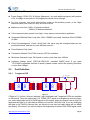
Chapter 1. Overview and Main Feature
4 digits 7segment panels are manufactured by Sure Electronics. This series
includes 5 different size panels, they are 1.5inches, 1.8inches, 2.3inches, and
4inches, 7inches (character height). All those panels are driven by SPI like
interface and all work in full static mode. They are easy to be interfaced to any
Microcontrollers. They could be widely used in panel meters, big clocks and any
other information display usage.
Sure Electronics provides series of such information boards which are supposed to
reduce your development time and make them standard. In this series, most
boards are 4 digits and static, if customer need any special digits and special size
ones, could contact us with the contact information at the end of this document. The
7 inch character height one is 1digit/board.
This document is used to describe how to use 1.5inches character height panels.
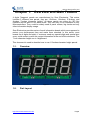
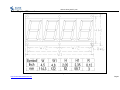
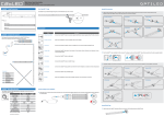
1-1.
Overview
Figure 1
1-2.
Part Layout
http://www.sure-electronics.com
Page2
We are here just for you!
Figure 2 Top Part Layout
Figure 3 Bottom Part Layout
1-3.
Main Feature
1-3-1. 4 digits 7-segment 1.5inches LEDs are installed on this panel, those
segments are common cathode type.
1-3-2. 2*10pin interface for power serializing and data transferring, data inputs
from J1 and flows out from J2.
1-3-3. A 74HC00 Nand chip is used to buffer CLK_IN and DIMM_IN control signal.
1-3-4. LED driver chips are composed of 4pcs of 74HC164, they are serialized to
each other, the first chip receives data from Microcontroller or the board ahead, the
final chip shifts data to next boards. Data should be clocked in from CLK_IN and
DATA_IN in J1, and DIMM_IN pin should be pull to high to enable display.
http://www.sure-electronics.com
Page3
We are here just for you!
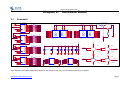
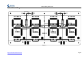
Chapter 2. Hardware Detail
Schematic
U5 74HC164
A0
A1
A2
A3
A4
A5
A6
A7
+5V
2
9
14
GND
A
CLK
B
CLR
VCC
QA
QB
QC
QD
QE
QF
QG
QH
3
4
5
6
10
11
12
13
R10
R11
R12
R13
R14
R15
R16
R17
131
131
131
131
131
131
131
561
B0
B1
B2
B3
B4
B5
B6
B7
D11501
7
6
4
3
2
9
10
8
D11501
A
B
C
D
E
F
G
DP
5
1
COM1
C0
C1
C2
C3
C4
C5
C6
C7
B0
B1
B2
B3
B4
B5
B6
B7
COM2
7
6
4
3
2
9
10
8
5
1
8 8
A
B
C
D
E
F
G
DP
COM2
A
B
C
D
E
F
G
DP
1
1
3
8 8
D11501
Q2 9014
A
B
C
D
E
F
G
DP
D0
D1
D2
D3
D4
D5
D6
D7
7
6
4
3
2
9
10
8
D11501
+5V
1
U4
R1
152
DIMM_OUT
1
8
7
6
4
3
2
9
10
8
U3
COM1
A0
A1
A2
A3
A4
A5
A6
A7
U2
COM1
U1
U6 74HC164
7
Q1 Not Installed
2
D
S
G
3
5
B
CLR
VCC
131
131
131
131
131
131
131
561
COM2
A
CLK
R2
R3
R4
R5
R6
R7
R8
R9
5
2
9
14
3
4
5
6
10
11
12
13
COM2
+5V
1
8
QA
QB
QC
QD
QE
QF
QG
QH
1
DATA_IN
CLK_OUT
GND
COM1
7
2
2-1
+5V
U7 74HC164
C8
1
C7
1
C6
1
C5
1
C9
CLK_IN
U8A
1
3
104
104
104
104
104
104
U8B
6
CLK_OUT
5
104
2
10V/100UF
2
10V/100UF
14
4
2
2
D0
D1
D2
D3
D4
D5
D6
D7
C4
2
131
131
131
131
131
131
131
561
+
C3
1
R26
R27
R28
R29
R30
R31
R32
R33
+
C2
2
3
4
5
6
10
11
12
13
14
C1
1
C0
C1
C2
C3
C4
C5
C6
C7
1
131
131
131
131
131
131
131
561
1
R18
R19
R20
R21
R22
R23
R24
R25
2
B
CLR
VCC
3
4
5
6
10
11
12
13
2
2
9
14
A
CLK
QA
QB
QC
QD
QE
QF
QG
QH
2
+5V
GND
1
1
8
2
7
7
74HC00
14
U8C
7
74HC00
14
U8D
U9 74HC164
7
1
8
+5V
2
9
14
GND
A
CLK
B
CLR
VCC
QA
QB
QC
QD
QE
QF
QG
QH
DATA_OUT
J1
+5V
DIMM_IN
DATA_IN
1
2
3
4
5
J2
6
7
8
9
10
+5V
CLK_IN
+5V
1
2
DIMM_OUT 3
DATA_OUT 4
5
CON10B
6
7
8
9
10
+5V
DIMM_IN
9
12
8
10
CLK_OUT
11
DIMM_OUT
13
7
74HC00
7
74HC00
CON10B
Figure 4
Note: Because of the LED's voltage drop difference, the resistance may vary from the value marked in the schematic.
http://www.sure-electronics.com
Page4
We are here just for you!
2-2
Physical Dimension
Figure 5
http://www.sure-electronics.com
Page5
We are here just for you!
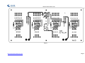
2-3
Circuit Diagram
Figure 6
http://www.sure-electronics.com
Page6
We are here just for you!
Figure 7
http://www.sure-electronics.com
Page7
We are here just for you!
2-4
Electric Characters
z Power Supply: DC4V-5.5V 0.2A/pcs (Maximum), for each additional panel, add another
0.2A, if voltage is less than 4V, the brightness would not be enough.
z For over 4 panels, user must add auxiliary power on the auxiliary power, or the 10pin
communication port could not carry so much current.
z Maximum clock freq: 1MHz, 4 boards serialized
100kHz, 20 boards serialized
z
If the communication speed is too high, it may cause communication problems.
z
Suggested Refresh Rate: Less than 10Hz if DIMM is not used. Less than 50Hz if DIMM
is used.
z
Drive Current/segment: 10mA +3mA/-2mA, this value may be changed based on the
production batch, and the dot uses different current.
z
Drive Method: Fully static.
z
Connection Method: 74HC164 in series, SPI like interface.
z
Maximum Cascade Level: 20 boards in series, clock less than 100kHz.
z
Interface Voltage Level: VDD*0.8-VDD+0.5V, standard CMOS level. If you need
TTL/CMOS compatible interface in batch, please contact us but the quantity should be
no less than 100pcs.
2-5
Port Definition
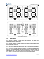
2-5-1. 7-segment LED
Q1 Not Installed
2
D
S
D11501
D11501
7
6
4
3
2
9
10
8
A
B
C
D
E
F
G
DP
1
5
5
1
8 8
D11501
3
1
U4
Q2 9014
A
B
C
D
E
F
G
DP
D11501
7
6
4
3
2
9
10
8
D0
D1
D2
D3
D4
D5
D6
D7
2
C0
C1
C2
C3
C4
C5
C6
C7
COM1
B0
B1
B2
B3
B4
B5
B6
B7
COM2
7
6
4
3
2
9
10
8
COM2
A
B
C
D
E
F
G
DP
U3
R1
152
DIMM_OUT
8 8
U2
COM1
5
5
1
COM1
A
B
C
D
E
F
G
DP
COM2
7
6
4
3
2
9
10
8
COM2
A0
A1
A2
A3
A4
A5
A6
A7
COM1
U1
1
1
G
3
Figure 8
4 Digits of 1.5 inches, common cathode, high brightness red 7-segment LEDs are installed
on this board. They are marked as U1-4. DIMM_OUT signal is for brightness control usage,
you could add simple on/off or PWM signal on this signal, when this signal is set to high, all
segments will light on if valid data is shifted out from the 74HC164 chip. If you are changing
the data in the 74HC164 driven chip, set this pin to low then the hash signal will not affect
the display. Of course if you want to adjust the brightness of those LEDs, PWM signal could
http://www.sure-electronics.com
Page8
We are here just for you!
be applied on the DIMM_IN pin. It is buffered with a 74HC00, and DIMM_OUT signal will
drive this board and next.
2-5-2. Shift Register Data Driver
U5 74HC164
7
DATA_IN
CLK_OUT
+5V
1
8
2
9
14
GND
A
CLK
B
CLR
VCC
QA
QB
QC
QD
QE
QF
QG
QH
U9 74HC164
3
4
5
6
10
11
12
13
R2
R3
R4
R5
R6
R7
R8
R9
131
131
131
131
131
131
131
561
A0
A1
A2
A3
A4
A5
A6
A7
7
1
8
2
9
14
+5V
GND
A
CLK
B
CLR
VCC
QA
QB
QC
QD
QE
QF
QG
QH
3
4
5
6
10
11
12
13
R26
R27
R28
R29
R30
R31
R32
R33
131
131
131
131
131
131
131
561
D0
D1
D2
D3
D4
D5
D6
D7
DATA_OUT
Figure 9
74HC164 is used as shift register in this board. They are U5, U6, U7, and U9 and
connected to U1-4. CLK_OUT is driven by a buffered output from CLK_IN with 74HC00.
DATA_IN is data input pin of the first 74HC164, then all 74HC164 of cascaded boards will
be serialized. All those pins accept only CMOS signals. Once you clock in correct data
through these 2 pins, and ensure that PWM signal or ON/OFF signal is applied correctly on
the DIMM_IN pin, the board will begin display.
Correspondence between Character Codes and Character Patterns:
Character
Patterns
0
1
2
3
4
5
6
7
8
9
Character
Codes
0xfc
0x60
0xda
0xf2
0x66
0xb6
0xbe
0xe0
0xfe
0xf6
Character
Patterns
a
b
c
d
E
f
g
h
i
j
Character
Codes
0xee
0x3e
0x1a
0x7a
0x9e
0x8e
0xf6
0x6e
0x60
0x70
Character
Patterns
l
n
o
p
Q
r
s
t
u
y
Character
Codes
0x1c
0x2a
0x3a
0xce
0xe6
0x0a
0xb6
0xe0
0x38
0x76
Figure 10
2-5-3. Data Ports Definition
J1
+5V
DIMM_IN
DATA_IN
1
2
3
4
5
J2
6
7
8
9
10
+5V
CLK_IN
+5V
1
2
DIMM_OUT 3
DATA_OUT 4
5
CON10B
6
7
8
9
10
+5V
CLK_OUT
CON10B
Figure 11
2 IDC sockets are located on the board. They are data input and output interface, marked
as J1 and J2. The definition is shown in Figure 11. When the board is working separately,
connect J1 to the Microcontroller board and leave J2 open. If lots of same boards are in
series, connect next board’s input to previous one’s output. Then you could connect up to
20 boards in series. Notice if over 4pcs of such boards are serialized, you must add
auxiliary power cable to some boards to enhance the current transfer.
2-5-4. Auxiliary Power Port
http://www.sure-electronics.com
Page9
We are here just for you!
AUX power
interface
AUX power
interface
Figure 12
There are 2 auxiliary power ports on this board. If you use less than 4pcs of such boards in
series, you could simply use a 10pin IDC flat cable to connect those boards. But if over 4
boards connected together, you must add additional power supply to some of those boards,
or the current may be lacking. Just apply +5V to some boards on the AUX power port. And
be sure the polarity is correct.
2-5-5. Data Buffer
+5V
14
CLK_IN
U8A
1
14
4
3
6
2
DIMM_IN
U8B
CLK_OUT
5
7
74HC00
14
U8C
9
7
74HC00
14
U8D
12
8
11
10
DIMM_OUT
13
7
74HC00
7
74HC00
Figure 13
74HC00 chip is used to buffer Clock and DIMM signal in this board. A CMOS chip is not
able to drive over 10pcs CMOS input if the cable is so long, here 74HC00 is used as NOT
gate, and 2 gates in series is a buffer.
http://www.sure-electronics.com
Page10
We are here just for you!
Chapter 3. Sample Codes
3-1.
LED Segment Drive Demo Board’s Schematic
+5V
R1
U1
PIC10F200
472
R2
472
ICSPDAT
1
CLK
R4
472
ICSPCLK
3
GP0/ICSPDAT
GP3/MCLR/VPP
GP1/ICSPCLK GP2/T0CKI/FOSC4
5
+5V
MCLR
6
4
R5
4
VDD
R3
472
472
DIMM
SW1
3
1
C1
2
DATA
VSS
1
2
2
104
J1
POWER
SW DIP-4
1
2
3
4
+5V
+12V
SW2
8
7
6
5
POWER
DIMM
DATA
CON10B
6
7
8
9
10
1
2
3
4
5
J2
POWER
MCLR
+5V
ICSPDAT
ICSPCLK
CLK
CON 6
1
2
3
4
5
6
J3
1
2
+12V
CON2
+5V
1
VOUT
3
+ C2
C5
C3
+
4
C4
VIN
1
D11N5817
2
1
1
1
DJ005B
1
2
3
1
J4
GND
U2 78M05/TO
104
100UF/10V
2
2
100uF/16V
2
2
104
Figure 14
3-2.
How to Connect Load
Power Supply form J3 or J4
DC 12V,1A Input
J4
+
- J3
LED Segment
Drive Demo
Board
1.5inch LED Board
J1
J1
J2
10 Pin IDC Flat Cable
Figure 15
http://www.sure-electronics.com
Page11
We are here just for you!
Output
Voltage
Encoder Position Setting(1)(2)
4 3 2 1
5V
+5V
ON
4 3 2 1
12V
+12V
OFF
4 3 2 1
0V
0V
Notice:
(1) DIP switch only has the 3 ways as shown above to work; any other switching ways are prohibited.
(2) Users shouldn’t change the voltage while LED Segment Drive Demo Board is working. It is only
allowed to change it before applying the current.
3-3.
How to display data with PIC10F200 and PICC8.05 environment
Source code is shown below,
#include <pic.h>
__CONFIG(UNPROTECT&MCLRDIS&WDTDIS);
#define
#define
#define
#define
Fuc_key
DIMM
CLK
DATA
//Configure Word
GP3
GP2
GP1
GP0
unsigned char disp_data;
unsigned char key_pressed,last_key_pressed;
unsigned char Value;
unsigned char time;
//The total of cathode
const unsigned char Digital_TAB[] = {0xff,0xfc,0x60,0xda,0xf2,0x66,0xb6,0xbe,0xe0,0xfe,0xf6,
0x80,0x40,0x20,0x10,0x08,0x04,0x02,0x01};
void change(void);
void LED_data(void);
void LED_display(void);
void delay_2ms(void)
{
unsigned char i, j, k;
http://www.sure-electronics.com
Page12
We are here just for you!
for(i = 0; i < 5; i++)
{
for(j = 0; j < 200; j++)
k--;
}
}
void change(void)
{
key_pressed=Fuc_key;
if((key_pressed==0)&(last_key_pressed==1))
{
delay_2ms();
if(key_pressed==0)
{
disp_data++;
if(disp_data==19)disp_data=0;
}
}
last_key_pressed=key_pressed;
}
void LED_data(void)
{
unsigned char i;
for(i = 0; i <19; i++)
{
if(i==disp_data){Value = Digital_TAB[i];}
}
}
void LED_display(void)
{
unsigned char i;
unsigned char U;
U=Value;
for(i = 0;i < 8; i++)
{
DATA = U & 0x01;
CLK = 0;
CLK = 1;
U = U>>1;
}
U=Value;
for(i = 0;i < 8; i++)
{
DATA = U & 0x01;
CLK = 0;
CLK = 1;
U = U>>1;
}
U=Value;
for(i = 0;i < 8; i++)
{
DATA = U & 0x01;
http://www.sure-electronics.com
Page13
We are here just for you!
CLK = 0;
CLK = 1;
U = U>>1;
}
U=Value;
for(i = 0;i < 8; i++)
{
DATA = U & 0x01;
CLK = 0;
CLK = 1;
U = U>>1;
}
}
void main(void)
{
OSCCAL=0;
TRIS = 0b11111000;
OPTION=0b10011111;
while(1)
{
change();
LED_data();
DIMM = 0;
LED_display();
DIMM = 1;
//Active–high Output Enable
delay_2ms();
}
}
http://www.sure-electronics.com
Page14
We are here just for you!
Chapter 4. Contact US
Sure Electronics Co., Ltd.
Floor 5, A zone,
Qinhuai Technology Innovation center,
NO.105-2, DaMing Road,
Nanjing,
China
Tel:
+8613601408832
+86-25-66606340
(English service, from GMT1-10AM, only for technical questions)
Email:
[email protected]
Website:
www.sure-electronics.net
www.sure-electronics.com
www.sureelectronics.net
http://www.sure-electronics.com
Page15