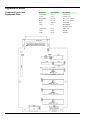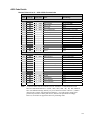
1
Digital488 and Digital488/32/OEM
IEEE 488 to Digital I/O Interface
IOtech, Inc.
25971 Cannon Road
Cleveland, OH 44146-1833
Phone: (440) 439-4091
Fax: (440) 439-4093
E-mail (Product Information): [email protected]
E-mail (Technical Support): [email protected]
Internet: www.iotech.com
Digital488 and
Digital488/32/OEM
IEEE488 to Digital I/O Interface
p/n 110-0901 Rev
© 1990… 2004 by IOtech, Inc.
916895
6.0
Printed in the United States of America.
Warranty Information
Your IOtech warranty is as stated on the product warranty card. You may contact IOtech by phone,
fax machine, or e-mail in regard to warranty-related issues.
Phone: (440) 439-4091, fax: (440) 439-4093, e-mail: [email protected]
Limitation of Liability
IOtech, Inc. cannot be held liable for any damages resulting from the use or misuse of this product.
Copyright, Trademark, and Licensing Notice
All IOtech documentation, software, and hardware are copyright with all rights reserved. No part of this product may be
copied, reproduced or transmitted by any mechanical, photographic, electronic, or other method without IOtech’s prior
written consent. IOtech product names are trademarked; other product names, as applicable, are trademarks of their
respective holders. All supplied IOtech software (including miscellaneous support files, drivers, and sample programs)
may only be used on one installation. You may make archival backup copies.
CE Notice
Many IOtech products carry the CE marker indicating they comply with the safety and emissions standards of the
European Community. As applicable, we ship these products with a Declaration of Conformity stating which
specifications and operating conditions apply.
Warnings, Cautions, Notes, and Tips
Refer all service to qualified personnel. This caution symbol warns of possible personal injury or equipment damage
under noted conditions. Follow all safety standards of professional practice and the recommendations in this manual.
Using this equipment in ways other than described in this manual can present serious safety hazards or cause equipment
damage.
This warning symbol is used in this manual or on the equipment to warn of possible injury or death from electrical
shock under noted conditions.
This ESD caution symbol urges proper handling of equipment or components sensitive to damage from electrostatic
discharge. Proper handling guidelines include the use of grounded anti-static mats and wrist straps, ESD-protective
bags and cartons, and related procedures.
This symbol indicates the message is important, but is not of a Warning or Caution category. These notes can be of
great benefit to the user, and should be read.
In this manual, the book symbol always precedes the words “Reference Note.” This type of note identifies the location
of additional information that may prove helpful. References may be made to other chapters or other documentation.
Tips provide advice that may save time during a procedure, or help to clarify an issue. Tips may include additional
reference.
Specifications and Calibration
Specifications are subject to change without notice. Significant changes will be addressed in an addendum or revision to
the manual. As applicable, IOtech calibrates its hardware to published specifications. Periodic hardware calibration is
not covered under the warranty and must be performed by qualified personnel as specified in this manual. Improper
calibration procedures may void the warranty.
Quality Notice
IOtech has been an ISO 9001 registered firm since 1996. Prior to shipment, we thoroughly test our products and
review our documentation to assure the highest quality in all aspects. In a spirit of continuous improvement,
IOtech welcomes your suggestions.
Table of Contents
1 - Introduction
3 - Command Descriptions
General Description …… 1-1
Bit Set An …… 3-1
Bit Clear Bn …… 3-1
Bus Input/Output Gn …… 3-2
Configure Cn …… 3-2
Data Dn....Z …… 3-3
Data Ready Rn …… 3-4
End or Identify (EOI) Kn …… 3-4
Execute X …… 3-5
Format Fn …… 3-5
Digital488 …… 1-1
Digital488/32/OEM …… 1-1
Available Accessories …… 1-2
Specifications …… 1-2
Digital488 Specifications …… 1-2
Digital I/O …… 1-2
IEEE 488 …… 1-3
General …… 1-3
Digital488/32/OEM Specifications …… 1-4
Digital I/O …… 1-4
IEEE 488 …… 1-4
General …… 1-5
F0 Format- ASCII Hexadecimal …… 3-5
F1 Format - ASCII Character …… 3-6
F2 Format - ASCII Binary …… 3-7
F3 Format - ASCII Decimal …… 3-7
F4 Format - Binary …… 3-8
F5 Format - High Speed Binary …… 3-8
Abbreviations …… 1-6
2 - Getting Started
Inspection …… 2-1
Configuration …… 2-1
Handshake Hn …… 3-9
Inhibit Qn …… 3-9
Invert In …… 3-9
Port Pn …… 3-10
Service Request Mask (SRQ) Mn …… 3-10
Serial Poll Status Byte …… 3-11
Status Un …… 3-12
Terminator Yn …… 3-14
Test T0 …… 3-15
IEEE 488 Address Selection …… 2-2
IEEE 488 Bus Output Terminator
Selection ……2-3
Digital Input/Output Ports …… 2-3
Logic Levels …… 2-3
Digital I/O Port Pin Outs …… 2-4
Control Lines …… 2-5
Clear …… 2-5
Data Strobe …… 2-5
External Data Ready [EDR] …… 2-6
Inhibit …… 2-6
Trigger …… 2-6
Service …… 2-7
IEEE 488 Bus Implementation …… 2-7
My Talk Address (MTA) …… 2-7
My Listen Address (MLA) …… 2-8
Device Clear (DCL and SDC) …… 2-8
Group Execute Trigger (GET) …… 2-8
Interface Clear (IFC) …… 2-8
Serial Poll Enable (SPE) …… 2-8
Serial Poll Disable (SPD) …… 2-8
Unlisten (UNL) …… 2-8
Untalk (UNT) …… 2-8
Installation …… 2-9
DaqBook/DaqBoard/Daq PC-Card User’s Manual
916895
Index-i
4 - IEEE 488 Primer
History …… 4-1
General Structure …… 4-1
Send It To My Address …… 4-3
Bus Management Lines …… 4-3
Attention (ATN) …… 4-3
Interface Clear (IFC) …… 4-3
Remote Enable (REN) …… 4-3
End or Identify (EOI) …… 4-3
Service Request (SRQ) …… 4-3
Handshake Lines …… 4-4
Data Valid (DAV) …… 4-4
Not Ready for Data (NRFD) …… 4-4
Not Data Accepted (NDAC) …… 4-4
Data Lines …… 4-4
Multiline Commands …… 4-5
Go To Local (GTL) …… 4-5
Listen Address Group (LAG) …… 4-5
Unlisten (UNL) …… 4-5
Talk Address Group (TAG) …… 4- 5
Untalk (UNT) …… 4-5
Local Lockout (LLO) …… 4-5
Device Clear (DCL) …… 4-5
Selected Device Clear (SDC) …… 4-5
Serial Poll Disable (SPD) …… 4-5
Serial Poll Enable (SPE) …… 4-5
Group Execute Trigger (GET) …… 4-5
Take Control (TCT) …… 4-5
Secondary Command Group (SCG) …… 4-5
Parallel Poll Configure (PPC) …… 4-6
Parallel Poll Unconfigure (PPU) …… 4-6
More On Service Requests …… 4-6
Serial Poll …… 4-6
Parallel Poll …… 4-6
5 - Service Information
Factory Service …… 5-1
Theory of Operation …… 5-1
Digital488 Mother Board …… 5-2
Digital488 I/O Board …… 5-4
Digital488/32/OEM …… 5-5
Digital488/OEM …… 5-6
Appendix A Digital488 Command Summary
Appendix B IEEE Command and Address
Messages
Appendix C Digital488/OEM Mechanical
Dimensions
ii
916895
DBK Option Cards & Modules User’s Manual
Introduction
1
General Description
Digital488
The Digital488/32/OEM is a board level interface with the same capabilities as the Digital488.
All descriptions in this manual refer to both products unless otherwise stated. When the model number
Digital488 is used in this manual, Digital488/32/OEM is also implied.
The Digital488 is a digital input and output interface to the IEEE 488 bus. Each unit has 40 TTL level
digital I/O lines, which are divided, into 5 eight-bit ports. Each port is software programmable as input
or output. The Digital488 has several features, which give it versatile interface capability. A trigger output
signal is asserted on the Group Execute Trigger (GET) command. Edge-triggered inputs can generate
a Service Request on the bus. Six data formats are software programmable, including ASCII hexadecimal,
ASCII character, ASCII binary, binary, high speed binary and ASCII decimal.
There are also individual bit set and bit clear commands. Programmable terminators are provided to
facilitate interfacing to various controllers.
A status mode enables the controller to interrogate the programmed status of the Digital488 at any time. A
self-test is initiated at power-on which checks for proper RAM and ROM operation.
When addressed to talk, the Digital 488 will output data from all forty bits or a selected 8-bit port. When
addressed to listen, the unit will input data and programming information from the controller and output the
data to the appropriate I/O port.
Digital488/32/OEM
The Digital488/32/OEM is a 4 in. by 4 in., 32 I/O line interface board for transferring data between the
IEEE 488 (GBIP, HP-IP) bus and devices equipped with up to 32-bit wide digital ports.
The Digital488/32/OEM’s 32 TTL-level digital I/O lines are programmable in 4-bit ports as either inputs
or outputs. When addressed to talk, the Digital488/32/OEM will output data from all thirty-two bits or a
selected 8 bit port. The board also offers six handshake lines for implementing clear, data strobe, external
data ready, inhibit, trigger, and SRQ functions. Its firmware includes a complete command set for
facilitating the implementation of all its functions. This command set is identical to that employed by the
other board-level and external interfaces in IOtech’s industry-standard Digital488 family, facilitating quick
prototyping and making the Digital488/32/OEM compatible with other Digital488 family units.
Digital488 User’s Manual
11-28-01
Introduction, 1-1
Available Accessories
Additional accessories that can be ordered for the Digital488 include:
CA-7-1
1.5 foot IEEE 488 Cable
CA-7-2
6 foot IEEE 488 Cable
CA-7-3
6 foot shielded IEEE 488 Cable
CA-7-4
6 foot reverse entry IEEE 488 Cable
CA-8-50†
6 foot, 50-conductor ribbon cable with a card edge
connector on one end, the other end un-terminated.
CA-46-40
6 foot digital I/O header connector to ribbon cable for the
Digital488/32/OEM
CN-6-50†
50 Pin solder tab edge connector.
CN-20
Right Angle IEEE 488 adapter, male and female
CN-22
IEEE 488 Multi-tap bus strip, four female connectors in parallel
CN-23
IEEE 488 panel mount feed-through connector, male
and female
Rack488-3†
5-1/4" by 19" rack mount for one Digital488
Rack488-4†
5-1/4" by 19" rack mount for two Digital488s
TR-2†
110 volt Wall mount power supply for the Digital488
TR-2E†
220 volt Wall mount power supply for the Digital488
TR-5
110 volt Wall mount power supply for the Digital488OEM
TR-5E
220 volt Wall mount power supply for the Digital488OEM
† For use with Digital488 Only
Specifications
Digital488 Specifications
Digital I/O
Terminal Installation Category:
Standard: Not Applicable. CE: Category 1.
Transistor-Transistor Logic (TTL) Levels:
Outputs will drive 2 TTL loads.
Connector:
One 50-pin card edge (mating connector supplied).
1-2, Introduction
11-28-01
Digital488 User’s Manual
IEEE 488
CAUTION
The IEEE 488 terminal must only be used to control a non-isolated IEEE 488 system.
The common mode voltage (cable shell to earth) must be zero.
Terminal Installation Category:
Standard: Not Applicable. CE: Category 1.
Implementation:
SH1, AH1, T6, TE0, L4, LE0, SR1, RL0, PP0, DC1, DT1, C0, E1.
Terminators:
Selectable CR, LF, LF-CR, and CR-LF with EOI.
Programmable:
IEEE Terminators, EOI, SRQ Mask, Port Data, Active Levels, Handshake Lines, Format and
Configuration.
Connector:
Standard IEEE 488 connector with metric studs.
General
Configuration:
Five 8-bit ports, programmable as inputs or outputs. Also included are programmable handshake lines,
data latching capability, Clear and Trigger outputs, and a Service Request (SRQ) input.
Terminal Installation Category:
Standard: Not Applicable. CE: Category 1 for all terminals.
Dimensions:
188 mm deep x 140 mm wide x 68 mm high (7.39" x 5.5" x 2.68").
Weight: 1.55 kg. (3.6 lbs).
Operating Environment:
Standard: Indoor, 0° to 50°C; 0 to 70% RH to 35°C. Linearly derate 3% RH/°C from 35 to 50°C.
CE: Indoor use at altitudes below 2000 meters, 0° to 40°C; 80% maximum RH up to 31°C decreasing
linearly 4% RH/°C to 40°C.
Controls:
Power switch (external), and IEEE parameter switches (internal).
Indicators:
LED indicators for IEEE TALK, LISTEN, SRQ, ERROR, and POWER.
Power:
An external power supply is provided with the Digital488: Input is 105-125 VAC,
or 210-250 VAC; 50/60 Hz, 10 VA maximum. The external power supply 9 VDC output
is to be connected to the Digital488 power input marked: 10 VDC MAX @ 500 mA.
WARNING
Do not use this interface outdoors. The interface is intended for indoor use only.
Outdoor conditions could result in equipment failure, bodily injury, or death.
CAUTION
Do not connect AC power line directly to the Digital488. Direct AC connection will
damage equipment.
Digital488 User’s Manual
11-28-01
Introduction, 1-3
Digital488/32/OEM Specifications
WARNING
Do not use this interface outdoors. The interface is intended for indoor use only.
Outdoor conditions could result in equipment failure, bodily injury, or death.
CAUTION
Never disassemble the interface case while it is connected to the AC power line.
Internal voltage potentials exist which could cause bodily injury or death.
Digital I/O
Configuration:
Four 8-bit ports, programmable as inputs or outputs.
Transistor-Transistor Logic (TTL) Levels:
Outputs will drive 2 TTL loads.
Connector:
One 40 pin header, organized as two rows of 20 pins.
IEEE 488
Implementation:
SH1, AH1, T6, TE0, L4, LE0, SR1, RL0, PP0, DC1, DT1, C0, E1.
Terminators:
Selectable CR, LF, LF-CR, and CR-LF with EOI.
Programmable:
IEEE Terminators, EOI, SRQ Mask, Port Data, Active Levels, Handshake Lines, Format and
Configuration.
Connector:
Standard IEEE 488 connector with metric studs.
1-4, Introduction
11-28-01
Digital488 User’s Manual
General
Configuration:
Four 8-bit ports, programmable as inputs or outputs. Also included are programmable
handshake lines, data latching capability, Clear and Trigger outputs, and a Service Request (SRQ)
input.
Dimensions:
101.6mm square x 16.51mm high (4” square x 0.65” high)
Weight: 0.13 kg. (0.29 lbs).
Operating Environment:
Standard: Indoor, 0° to 50°C; 0 to 70% RH to 35°C. Linearly derate 3% RH/°C from 35 to 50 °C.
Controls:
IEEE parameter switches.
Indicators:
On-board and 10 pin header for remote use. The external LEDs are connected to VCC through a
resistor network. The pin-out table for the LED status header is located in Figure 1.1.
PIN #
1
2
3
4
5
6
7
8
9
10
LED CONNECTOR
Error (Cathode)
Error (Anode)
SRQ (Cathode)
SRQ (Anode)
Listen (Cathode)
Listen (Anode)
Talk (Cathode)
Talk (Anode)
Power (Cathode)
Power (Anode)
Figure 1.1: LED Indicators
Power:
User supplied +5 volts ±0.25% at 1 amp. Mating power connector with 8-inch leads provided.
WARNING
Do not use this interface outdoors. The interface is intended for indoor use only.
Outdoor conditions could result in equipment failure, bodily injury, or death.
CAUTION
Never disassemble the interface case while it is connected to the AC power line.
Internal voltage potentials exist which could cause bodily injury or death.
Digital488 User’s Manual
11-28-01
Introduction, 1-5
Abbreviations
The following IEEE 488 abbreviations are used throughout this manual.
addr n
ATN
CA
CR
data
DCL
GET
GTL
LA
LAG
LF
LLO
MLA
MTA
PPC
PPU
SC
SDC
SPD
SPE
SRQ
TA
TAD
TCT
term
UNL
UNT
*
1-6, Introduction
IEEE bus address "n"
Attention line
Controller Active
Carriage Return
Data String
Device Clear
Group Execute Trigger
Go To Local
Listener Active
Listen Address Group
Line Feed
Local Lock Out
My Listen Address
My Talk Address
Parallel Poll Configure
Parallel Poll Unconfigure
System Controller
Selected Device Clear
Serial Poll Disable
Serial Poll Enable
Service Request
Talker Active
Talker Address
Take Control
Terminator
Unlisten
Untalk
Unasserted
11-28-01
Digital488 User’s Manual
Getting Started
2
Inspection
The unit was carefully inspected, both mechanically and electrically, prior to shipment.
When you receive the interface, carefully unpack all items from the shipping carton and check for any
obvious signs of physical damage, which may have occurred during shipment. Report any such damage
found to the shipping agent immediately. Remember to retain all shipping materials in the event that
shipment back to the factory becomes necessary.
Every Digital488 is shipped with the following....
• Digital488
IEEE Digital I/O Converter
• CN-8-50
Digital I/O Port Mating Connector
• Digital488 User’s Manual
• Power Supply TR-2; 115V or
• TR-2E; 220V
Every Digital488/32/OEM is shipped with the following....
• Digital488/32/OEM
IEEE Digital I/O Converter
• Digital488 User’s Manual
• CA-106 1 foot ribbon cable to IEEE488 connector
• Macro488OEM-002 Power Plug Assembly
Configuration
The Digital488 has one internal 8 position switch which determines the unit's IEEE address and its default
IEEE bus output terminator. The switch is only read when the unit is powered on, and should only be set
prior to applying power. The following figure illustrates the factory default setting for SW1.
SW1 Factory Default Settings
To modify any of these defaults, follow this simple procedure. Disconnect the power supply from the AC
line and from the interface. Disconnect any IEEE or digital I/O cables prior to disassembly.
Digital488 User’s Manual
11-19-01
Getting Started, 2-1
WARNING
Never open the Digital488 case while it is connected to the AC line. Failure to
observe the warning may result in equipment failure, personal injury or death.
Remove the four screws located in each corner of the rear panel. Hold the case firmly and pull the rear
panel outward, noting the slot location of the main circuit board. Modify those parameters, which are
appropriate for your installation and reassemble the unit. Slide the main circuit board into the previously
noted slot and finish reassembly by tightening the four screws into the rear panel.
IEEE 488 Address Selection
The IEEE 488 bus address is set by SW1-1 through SW1-5. The address can be set from 0 through 30 and
is read only at power on. The address is selected by simple binary weighting with SW1-1 being the least
significant bit and SW1-5 the most significant bit. The factory default is address 18.
If address 31 is selected, it defaults to address 30 because the IEEE 488 standard has reserved address 31.
SW1 View for IEEE Bus Address Selection
2-2, Getting Started
11-19-01
Digital488 User’s Manual
IEEE 488 Bus Output Terminator Selection
The terminating characters sent on output by the Digital488 are determined by SW1-6 through SW1-8.
The terminator switches are read only at power on, but can be changed by the controller through the
Terminator command. If power is cycled after receipt of the Terminator command, then the unit will
again default to the switch settings. The factory default settings are Carriage Return - Line Feed with EOI
asserted.
The Digital488 ignores all terminators received from the bus controller. Only the Execute command (X)
is used to signal the Digital488 that a command string has been completed.
SW1 View for Terminator Selection
Digital Input/Output Ports
The Digital488 has 40 data lines, which can be programmed in groups of 8 as either input or output.
At power on, all 40 bits are in the input mode. Each 8 bit group is one port, beginning with Port 1 as the
least significant 8 bits, and Port 5 as the most significant 8 bits.
The Digital488/32/OEM has 32 data lines, which can be programmed in groups of 8 as either input
or output. Each 8 bit group is one port, beginning with Port 1 as the least significant 8 bits,
and Port 4 as the most significant 8 bits.
Logic Levels
The data and handshake output lines will drive two TTL loads. In addition, ports 1 and 2 outputs are 5 Volt
CMOS compatible. All input lines are less than 1.5 TTL loads. All inputs are protected against damage due
to high static voltages. Normal precautions should be taken to limit the input voltages to -0.3 to +7.0 volts.
All I/O lines are referenced to COMMON (Pin 50).
Digital488 User’s Manual
11-19-01
Getting Started, 2-3
Digital I/O Port Pin Outs
The following diagram illustrates the digital I/O edge connector as view from the rear of the Digital488 and
the top PC Board edge view of the Digital488/32/OEM.
Digital488 Rear Panel I/O Connector Pin Out
Pin
Digital488
1 thru 8
Least Significant Port
9 thru 16
17 thru 24
25 thru 32
33 thru 40
Most Significant Port
41
42
43
44
45
46
47,48
49
50
2-4, Getting Started
Digital488/32/OEM I/O Connector Pin Out
Description
DATA PORT1 (Input or Output).
Pin 1 is bit 1 (LSB), Pin 8 is bit 8 (MSB).
DATA PORT2 (Input or Output)
Pin 9 is bit 1 (LSB), Pin 16 is bit 8 (MSB)
DATA PORT3 (Input or Output)
Pin 17 is bit 1 (LSB), Pin 24 is bit 8 (MSB)
DATA PORT4 (Input or Output)
Pin 25 is bit 1 (LSB), Pin 32 is bit 8 (MSB)
DATA PORT5 (Input or Output
Pin 33 is bit 1 (LSB), Pin 40 is bit 8 (MSB)
CLEAR (Output)
DATA STROBE (Output)
TRIGGER (Output)
INHIBIT (Output)
SERVICE INPUT (Input).
EXTERNAL DATA READY [EDR] (Input)
Not used
+5 Volts (Do not exceed 50 mA load)
I/O COMMON (Gnd)
11-19-01
Pin
Digital488/32/OEM
1 thru 8
Least Significant Port
9 thru 16
17 thru 24
25 thru 32
Most Significant Port
N/A
33
37
34
38
35
36
N/A
39
40
Digital488 User’s Manual
Control Lines
Six control lines enable handshaking of digital I/O data transfer to the Digital488. They are automatically
activated with the corresponding I/O activity and can be independently activated with the
Handshake (Hn) command. Note that the pin numbers for the Digital488/32/OEM are different from
the pin numbers for the Digital488.
Clear (Digital488:
Digital488/32/OEM:
Pin 41
Pin 33)
The Clear output is pulse for approximately 50 microseconds after a Device Clear (DCL), Selected Device
Clear (SDC), or Interface Clear (IFC) command has been sent on the bus. The Clear line is normally active
high. The Invert command (I8) will program it active low. The Handshake command (H0) can pulse the
Clear line, independent of any I/O operations.
Timing Diagram for Clear Output
Data Strobe (Digital488:
Digital488/32/OEM:
Pin 42
Pin 37)
The Data Strobe output is pulse for approximately 50 microseconds after new data is output on the
I/O port. The Data Strobe line is normally active high but may be programmed active low by the Invert
command (I4). The Handshake command (H1) can pulse the Data Strobe line, independent
of an I/O operation.
Timing Diagram for Strobe Output
Digital488 User’s Manual
11-19-01
Getting Started, 2-5
External Data Ready [EDR] (Digital488:
Digital488/32/OEM:
Pin 46
Pin 36)
The External Data Ready [EDR] line is an edge sensitive input which is used to latch input data. It is used
in conjunction with the Data Ready command (R1). The EDR signal must be at least 1 microsecond wide
and must have a rise and fall time of less than one microsecond. The EDR line is normally rising-edge
sensitive but can be programmed with the Invert command (I32) to be falling-edge sensitive.
Refer to the following diagram for timing relationships.
When using the EDR line with the R1 command, data is not read when the Digital488 is addressed to talk
as with R0. The Digital488 will only output data when the EDR line transitions.
EDR is not functional in the high-speed binary (F5) format.
Inhibit (Digital488:
Digital488/32/OEM:
Pin 44
Pin38)
The Inhibit output is asserted while data on the selected I/O port is being read into the I/O port buffer.
This line is normally active high but may be programmed active low by the Invert command (I1).
The Inhibit line can be programmed independent of any I/O operations with the Inhibit command (Qn).
Refer to the following diagram for timing relationships.
The Inhibit line is asserted once for each data read operation for all format [Fn] modes except high-speed
binary [F5]. In this mode, it is asserted for the first data read after the Digital488 is addressed to talk.
On the last data-byte transfer, the data is read again with Inhibit asserted in anticipation of another data
transfer. If Inhibit is used to sequence external hardware, you should be aware that this line will pulse N+1
times; where N is the number of total (5 byte) data transfers.
Timing Diagram for EDR Input and Inhibit Output
Trigger (Digital488:
Digital488/32/OEM:
Pin 43
Pin34)
The Trigger output is pulse for approximately 50 microseconds after a GET (Group Execute Trigger)
command is received from the bus controller. The trigger pulse is normally active high, but can be made
active low with the Invert command (I2). The Handshake command (H2) can independently pulse the
Trigger line, independent of any bus activity.
Timing Diagram for Trigger Output
2-6, Getting Started
11-19-01
Digital488 User’s Manual
Service (Digital488:
Digital488/32/OEM:
Pin 45
Pin35)
The Service input is an edge sensitive input capable of generating a bus Service Request (SRQ).
It is enabled with the SRQ command (M1) and defaults to rising-edge sensitive. The Invert command
(I64 ) can be used to program it to be falling-edge sensitive.
IEEE 488 Bus Implementation
The Digital488 implements many of the capabilities defined by the IEEE 488 1978 specification.
These are discussed in the following sections. Those bus uniline and multiline commands that the
Digital488 does not support or respond to include:
Remote Enable (REN)
Go to Local (GTL)
Local Lockout (LLO)
Take Control (TCT)
Parallel Poll (PP)
Parallel Poll Configure (PPC)
Parallel Poll Unconfigure (PPU)
Parallel Poll Disable (PPD)
My Talk Address (MTA)
When the Digital488 is addressed to talk (R0) it asserts Inhibit, reads the data from all ports, un-asserts
Inhibit and outputs the data to the bus in the format as defined by the Fn, Pn and Gn commands.
The output bus terminators are appended to the output with the exception of the F4 and F5 formats.
F4 does not append terminators. The output format of F5 will be described separately. After output in the
F0 through F4 formats, the Digital488 must be re-addressed to talk to perform subsequent reads.
In the R1 mode, it will wait for the selected EDR transition before reading the data and formatting it for
output. If the EDR line has transitioned prior to being addressed to talk, the data read at the time of EDR
will be buffered for output when next addressed to talk. If EDR transitions again before the previous EDR
buffered data has been output, the Digital488 will generate an EDR Overrun error and ignore the EDR
read request. After output in the F0 through F4 formats, the Digital488 must be re-addressed to talk
to perform subsequent buffered output of EDR captured data.
In either Rn mode, the Digital488 can send requested status (Un) without affecting the data ports
or Inhibit. After the requested status is output, the presently programmed Rn mode returns.
EDR cannot be used to capture data in the high-speed binary format (F5). When addressed to talk in this
format it asserts Inhibit, reads the data from all ports, un-asserts Inhibit and outputs the binary data to the
bus with EOI asserted on the fifth byte. When the last data byte is transferred, the data is read again
in anticipation of another data transfer. If Inhibit is used to sequence external hardware, this line will pulse
N+1 times; where N is the number of total (5 byte) data transfers. In this format, the Digital488 does not
have to be re-addressed to talk to read the ports multiple times.
With all Fn formats, using the Digital488 the data is output in a PORT5, PORT4, PORT3, PORT2, PORT1
sequence. Using the Digital488/32/OEM the data is output in a PORT4, PORT3, PORT2, PORT1
sequence.
Digital488 User’s Manual
11-19-01
Getting Started, 2-7
My Listen Address (MLA)
When the Digital488 is addressed to listen in the F0 through F4 format, it accepts characters from the
active talker and interprets these characters as commands and command parameters. These commands are
explained in Chapter 3.
In the high-speed binary format (F5), the command interpreter is disabled. The Digital488 treats all bytes
received as data to be output to the Digital I/O ports. Each time it receives five bytes or detects EOI
it pulses the Data Strobe for approximately 15 microseconds. Using the Digital488 data is expected I
n a PORT5, PORT4, PORT3, PORT2, PORT1 sequence. Using the Digital488/32/OEM data is expected
in a PORT4, PORT3, PORT2, PORT1 sequence.
If only two bytes are received, with EOI asserted on the second byte, the Digital488 will update PORT5
with the first byte received PORT4 with the second and pulse the Data Strobe.
If using Digital488/32/OEM will update PORT4 with the first byte received, and PORT3 with the second
and pulse the Data Strobe. Since the interface treats all received characters as data, the Status (Un)
command will not be recognized.
Device Clear (DCL and SDC)
In the F0 thru F4 formats, Device Clear resets the Digital488 to power on defaults and pulses the Clear
output line for approximately 50 microseconds.
In the high-speed binary format (F5), it enables the command interpreter and changes the format to F0. All
other parameters remain unchanged. In addition, the Clear output line is not pulsed by DCL or SDC when
the interface is in F5. This is the only programmable method to exit the F5 format.
Group Execute Trigger (GET)
When the Digital488 recognizes a GET, it pulses the Trigger output line for approximately 50
microseconds.
Interface Clear (IFC)
IFC places the Digital488 in the Talker/Listener Idle State and pulses the Clear output line for
approximately 50 microseconds.
Serial Poll Enable (SPE)
When Serial Poll Enabled, the Digital488 sets itself to respond to a serial poll with its serial poll status byte
if addressed to talk. When the serial poll byte is accepted by the controller, any pending SRQs are cleared.
The Digital488 will continue to try to output its serial poll response until it is serial poll disabled by the
controller.
Serial Poll Disable (SPD)
Disables the Digital488 from responding to serial polls by the controller.
Unlisten (UNL)
UNL places the Digital488 in the Listener Idle State.
Untalk (UNT)
UNT places the Digital488 in the Talker Idle State.
2-8, Getting Started
11-19-01
Digital488 User’s Manual
Installation
To begin operating the Digital488, plug the external power supply into the rear jack on the interface.
CAUTION
Never install the power supply into the interface while it is connected to AC line
power. Failure to observe this caution may result in damage to the Digital488.
WARNING
Do not use this interface outdoors. The interface is intended for indoor use only.
Outdoor conditions could result in equipment failure, bodily injury, or death.
After installing the power supply connector into the interface, turn on the Digital488 by depressing the rear
panel power switch. All the front panel LEDs should light for approximately one second while the
Digital488 performs an internal ROM and RAM self check. At the end of this self-check, all indicators
should turn off except POWER.
If you obtain the above response then your Digital488 is alive and well. If all LEDs remain on, then
a ROM error has occurred. If all LEDs continue to flash (except the power LED), then a RAM error has
occurred. Try cycling the power to the Digital488 to determine that the error is repeatable.
If the LEDs do not flash and the POWER indicator does not remain lit, there may not be any power
supplied to the interface. In this event, check to make sure the AC power is supplied to the power supply,
and that the supply is properly installed into the unit. If the problem is unresolved, refer to the
Service Information section of this manual.
Digital488 User’s Manual
11-19-01
Getting Started, 2-9
2-10, Getting Started
11-19-01
Digital488 User’s Manual
Command Descriptions
3
Control of the Digital 488 is implemented with 17 bus commands, described here in detail. Examples are
given for many of the commands using a Hewlett-Packard 85 computer in the immediate mode. It is
implied that each command is terminated by the 'END LINE' key on the HP-85 in order to execute the
command. The Digital488 bus address should be set to 18 for all examples.
It is necessary that the EXECUTE command (X) follow all command strings sent to the
Digital488. No commands are executed until an X is received by the Digital488.
Bit Set
An
The Bit Set command programs a logic one output to a bit described by the argument 'n'. Setting a bit may
represent either a +5 volt or 0 volt output, depending on whether an Invert command (I16) has been sent.
If data is active high (default condition), then Bit Set outputs +5 volts. If multiple bits are to be set within
the same command string, an Execute command (X) must be included after every Bit Set command.
The bit which is being set must have been configured as an output bit by the Configure command to be
valid. The Strobe output line is not pulsed when the Bit Set command is sent.
An
Bit n (1 thru 40) is set to logic one
Example:
CLEAR 718
OUTPUT 718;"C5X"
OUTPUT 718;"A22X"
OUTPUT 718;"A23XA24X"
reset the Digital488
configure all ports as output
set bit 22 to a logic one
set bits 23 and 24 to a logic one
Bit Clear
Bn
The Bit Clear command will clear to a logic zero an output bit described by the argument 'n'. Clearing
a bit may represent either a 0 volt or +5 volt output, depending on whether an Invert command (I16) has
been sent. If data is active high (default condition), then Bit Clear outputs 0 volts. When multiple
Bit Clear commands are used in the same command string, an Execute command (X) must follow each
command.
The bit that is being cleared must have been defined as an output by the Configure command in order
to be valid. The Strobe output line is not pulsed when the Bit Clear command is sent.
Bn
Bit n (1 thru 40) is cleared to a logic 0
Example:
CLEAR 718
OUTPUT 718;"C5X"
OUTPUT 718;"A7XA8XA9X"
OUTPUT 718;"B7X"
OUTPUT 718;"B8XB9X"
Digital488 User’s Manual
7-17-01
reset the Digital488
configure all ports as output
set bits 7, 8, and 9 to +5 volts
clear bit 7 to zero volts
clear bits 8 and 9 to zero volts
Command Descriptions, 3-1
Bus Input/Output
Gn
The Bus Output command determines whether input port data, output port data or both will be transmitted
on the bus when the Digital488 is addressed to talk. The amount of data sent is dependent
on the Pn command.
The G0 default mode causes all input and output port data to be sent to the controller when addressed
to talk. The G1 mode causes only data from the ports programmed as inputs to be returned when addressed
to talk. The G2 mode causes only data from ports programmed as outputs to be returned when addressed
to talk.
If all ports are programmed as outputs with G1 selected and the Digital488 is addressed to talk,
nothing will be transmitted and the bus will hang. The converse will also cause the bus to hang with all
ports programmed as inputs and G2 selected.
Input and output port data is send on talk
Only input port data is sent on talk
Only output port data is sent on talk
G0
G1
G2
Example:
CLEAR 718
OUTPUT 718;"P0C1X"
OUTPUT 718;"G1X"
ENTER 718; A$
DISP A$
reset the Digital488
port1 as output, ports 2-5 as input
select only input ports
read data from the input ports
display shows FFFFFFFF (data is
dependent on what is connected.
OUTPUT 718;"G2X"
ENTER 718; A$
DISP A$
select output ports
read data from the output ports
display shows 00 (outputs default to 0)
Configure
Cn
Ports 1 thru 5 are configured as inputs or outputs with the Configure command.
Each port is eight bits wide. At power-on, all ports are initialized as inputs. The Configure command is
usually the first command to be sent after power on. All ports programmed as outputs will be set to a logic
zero after receiving the Configure command. The actual output level is dependent on the Invert command
(I16).
Cn
Mode n (0 thru 5) defines which ports are input and output
Port
C0
C1
C2
C3
C4
C5
5
in
in
in
in
in
out
4
in
in
in
in
out
out
3
in
in
in
out
out
out
2
in
in
out
out
out
out
1
in
out
out
out
out
out
in = programmed as an input port
out = programmed as an output port
Example:
CLEAR 718
OUTPUT 718;"C1X"
3-2, Command Descriptions
reset the Digital488
select port 1 as output, ports 2 thru 5
as inputs
7-17-01
Digital488 User’s Manual
Data
Dn....Z
The Data command outputs up to 40 bits of data to the output ports. The number of bits, which can be sent
with the Data command, is limited by the number of bits programmed as outputs. For formats
F0 through F3, if the amount of data sent is less than the number of bits programmed as outputs,
the least-significant bits will contain the data sent and the most-significant bits will be cleared to logic zero.
If a single port is selected with the Port command, only eight bits may sent with the Data command.
The Data Strobe output is pulse for approximately 50 microseconds after new data is output on the
selected ports.
For formats F0 through F3, data sent by the controller is contained within a prefix (D) and a suffix (Z).
In format F4, the five bytes immediately following the prefix (D) is interpreted as data and the suffix (Z)
is not used. For the high-speed binary F5 format, all bytes received are treated as data and the prefix and
suffix are not used. Refer to the Fn command for additional details.
Dn...Z n... represents the data to be outputted, terminated by Z.
In the F4 mode, the Z terminator is not allowed
Example:
CLEAR 718
OUTPUT 718;"C5P1X"
OUTPUT 718;"D55ZX"
ENTER 718; A$
DISP A$
reset the Digital488
all ports as output, select port 1
send 55 to port 1
read data from port 1
display shows 55
OUTPUT 718;"P0X"
OUTPUT
718;"D1234567890ZX"
ENTER 718;A$
DISP A$
select all ports
send data to all 40 bits
OUTPUT 718;"D123ZX"
ENTER 718; A$
DISP A$
send 12 bits of data to the least significant bits
read data from the Digital488
display shows 0000000123
OUTPUT
718;"P5D21ZX"
OUTPUT 718;"P0X"
ENTER 718; A$
DISP A$
set port 5 only
Digital488 User’s Manual
read data from the Digital488
display shows 1234567890
select all ports
read data from the Digital488
display shows 2100000123
7-17-01
Command Descriptions, 3-3
Data Ready
Rn
The Data Ready command enables digital input data to be latched. When used in conjunction with the
Service Request (M2) command, the External Data Ready line can both latch the input data and signal
the controller that new data is available.
In the default mode, (R0) data is read when the Digital488 is addressed to talk. In the R1 mode, it will wait
for the selected External Data Ready (EDR) transition before reading the data and formatting it for
output. If the Digital488 is addressed to talk before EDR is asserted, the bus will hang up until the EDR
pulse occurs. Once EDR is asserted, the data will remain latched until the interface is addressed to talk and
the data is read by the controller. If EDR transitions again before the previous EDR buffered data has been
output, the Digital488 will generate an EDR Overrun error and ignore the EDR read request.
After output in the F0 through F4 formats, the Digital488 must be re-addressed to talk to perform
subsequent buffered output of EDR captured data. EDR cannot be used to capture data
in the F5 high-speed binary format
The EDR signal must be at least 1 microsecond wide and should have a rise and fall time of less than 1.0
microsecond. The EDR line defaults to rising-edge sensitive but can be changed to falling-edge sensitive
with the Invert command (I32).
R0
R1
Data is not latched, and is read whenever the Digital488
is addressed to talk
Data is latched on an EDR transition
Example:
CLEAR 718
OUTPUT 718;"R1X"
reset the Digital488
data is only read after a rising-edge
signal is applied to the EDR
line
End or Identify (EOI)
Kn
The EOI line is one of five interface management lines on the IEEE 488 Bus. It is used by a talker
to indicate the end of a multiple byte transfer sequence. At power-on, the setting of Switch S1 determines
the default EOI mode. The controller can change the EOI mode by programming the Digital488 from
the bus. In the K0 mode, the EOI line is asserted by the Digital488 on the last byte of every bus output
string. In the K1 mode the EOI function is disabled (except when using the binary modes [F4 and F5]).
K0
K1
EOI enabled, assert EOI on last byte transferred
EOI disabled, do not assert EOI on last byte transferred
Example:
OUTPUT 718;"K1X"
3-4, Command Descriptions
disables EOI on last byte
7-17-01
Digital488 User’s Manual
Execute
X
Commands sent to the Digital488 will result in no action until the unit is instructed to execute these
commands. This is done by sending an X, usually as the last character of a command string.
Commands sent without an X are stored in the internal buffer until an X is received. Any number
of Execute commands may be inserted into the same command string. Certain commands, such as Bit Set
require an X after each command in a string if more than one of that command is within the same string.
Example:
CLEAR 718
OUTPUT 718;"F2"
OUTPUT 718;"X"
OUTPUT 718;"A1XA2X"
reset the Digital488
send "F2" to the Digital488 command
input buffer
instruct the Digital488 to execute its
command input buffer
Two Bit Set (A) commands are within
the same string, requiring an X after
each command.
Format
Fn
The Format command determines the method by which input and output data will be described.
Six data formats are available.
F0
F1
F2
F3
F4
F5
ASCII Hexadecimal (4 bits per character)
ASCII Character (4 bits per character )
ASCII Binary (1 bit per character)
ASCII Decimal (8 bits per number)
Binary (each byte represents 8 bits)
High Speed Binary (each byte represents 8 bits)
F0 Format- ASCII Hexadecimal
In the default F0 format, the data is described in ASCII hexadecimal, with each character having a value
from 0 thru 9 or A thru F. Each ASCII character describes 4 bits of data.
F0 Character
0
1
2
3
4
5
6
7
Decimal Equiv
0
1
2
3
4
5
6
7
F0 Character
8
9
A
B
C
D
E
F
Decimal Equiv
8
9
10
11
12
13
14
15
Data received for output to the digital ports must be contained within a prefix (D) and a suffix (Z).
If the amount of data sent is less than the number of bits programmed as outputs, the least-significant bits
will contain the data sent and the most-significant bits will be cleared to logic zero. If the data sent
is greater than the number of bits programmed for output or selected by the Pn command, the Digital488
will generate a conflict error and ignore the entire command string. The Data Strobe output is pulse for
approximately 50 microseconds after new data is output on the selected port(s).
Digital488 User’s Manual
7-17-01
Command Descriptions, 3-5
When the Digital488 is addressed to talk (R0) it asserts Inhibit, reads the data from all ports, unasserts
Inhibit and outputs the number of characters determined by the Gn and Pn commands. Leading zeros are
not suppressed and the bus terminators are appended to the output. After output the Digital488 must
be re-addressed to talk to perform subsequent reads. EDR (R1) may also be used to capture data in this
format.
Example:
DIM A$[50]
CLEAR 718
OUTPUT 718;"C2G2X"
OUTPUT 718;"D4E6BZX"
ENTER 718; A$
DISP A$
dimension the length of A$
reset the Digital488
configure ports 1 & 2 as output
output hexadecimal 4E6B to ports 1 & 2
read data from the Digital488
display shows 4E6B
F1 Format - ASCII Character
In the F1 format, the data is coded and transmitted in ASCII Characters with the four least significant bits
of each ASCII character representing four bits of data.
F1 Character
0
1
2
3
4
5
6
7
Decimal Equiv
0
1
2
3
4
5
6
7
F1 Character
8
9
:
;
<
=
>
?
Decimal Equiv
8
9
10
11
12
13
14
15
Data received for output to the digital ports must be contained within a prefix (D) and a suffix (Z).
If the amount of data sent is less than the number of bits programmed as outputs, the least-significant bits
will contain the data sent and the most-significant bits will be cleared to logic zero. If the data sent
is greater than the number of bits programmed for output or selected by the Pn command, the Digital488
will generate a conflict error and ignore the entire command string.
The Data Strobe output is pulse for approximately 50 microseconds after new data is output on the
selected port(s).
When the Digital488 is addressed to talk (R0) it asserts Inhibit, reads the data from all ports, unasserts
Inhibit and outputs the number of characters determined by the Gn and Pn commands. Leading zeros are
not suppressed and the bus terminators are appended to the output. After output the Digital488 must
be re-addressed to talk to perform subsequent reads. EDR (R1) may also be used to capture data in this
format.
Example:
OUTPUT 718;"F1X"
ENTER 718; A$
DISP A$
OUTPUT 718;"D1??2ZX"
ENTER 718; A$
DISP A$
3-6, Command Descriptions
select ASCII Character format
read data from the Digital488
display shows 4>6;
send 1??2 to the Digital488
read data from the Digital488
display shows 1??2
7-17-01
Digital488 User’s Manual
F2 Format - ASCII Binary
In the F2 format, the each data bit is described with an ASCII 0 or 1. Each byte is formatted in two 4-bit
multiples separated by semicolons.
F2 String
0000;0000
0000;0001
0000;0010
0000;0011
0000;0100
0000;0101
0000;0110
0000;0111
0000;1000
Decimal Equiv
0
1
2
3
4
5
6
7
8
F2 String
0000;1001
0000;1010
0000;1011
0000;1100
0000;1101
0000;1110
0000;1111
1000;0001
1111;1111
Decimal Equiv
9
10
11
12
13
14
15
129
255
Data received for output to the digital ports must be contained within a prefix (D) and a suffix (Z) and each
4-bit quantity must be separated by semicolons. Leading zeros are not required. If the amount of data sent
is less than the number of bits programmed as outputs, the least-significant bits will contain the data sent
and the most-significant bits will be cleared to logic zero. If the data sent is greater than the number of bits
programmed for output or selected by the Pn command, the Digital488 will generate a conflict error and
ignore the entire command string. The Data Strobe output is pulse for approximately 50 microseconds
after new data is output on the selected port(s).
When the Digital488 is addressed to talk (R0) it asserts Inhibit, reads the data from all ports, unasserts
Inhibit and outputs the number of characters determined by the Gn and Pn commands. Leading zeros are
not suppressed and the bus terminators are appended to the output. After output the Digital488 must be readdressed to talk to perform subsequent reads. EDR (R1) may also be used to capture data in this format.
Example:
OUTPUT 718;"F2X"
ENTER 718;A$
DISP A$
OUTPUT 718;"D1111;0;1010;0101ZX"
ENTER 718; A$
DISP A$
select ASCII/binary mode
read data from the Digital488
display shows 0001;1111;1111;0001
read data from the Digital488
display shows 1111;0000;1010;0101
F3 Format - ASCII Decimal
In the F3 format, the data is described in decimal 8 bit multiples and transmitted in ASCII. Each decimal
number (0 to 255) to be output must be separated by semicolons.
F3 Number
000
001
002
003
004
005
006
007
Digital488 User’s Manual
Decimal Equiv
0
1
2
3
4
5
6
7
7-17-01
F3 Number
008
009
010
020
100
200
210
255
Decimal Equiv
8
9
10
20
100
200
210
255
Command Descriptions, 3-7
Data received for output to the digital ports must be contained within a prefix (D) and a suffix (Z).
If the amount of data sent is less than the number of bits programmed as outputs, the least-significant bits
will contain the data sent and the most-significant bits will be cleared to logic zero. If the data sent
is greater than the number of bits programmed for output or selected by the Pn command, the Digital488
will generate a conflict error and ignore the entire command string. The Data Strobe output is pulse for
approximately 50 microseconds after new data is output on the selected port(s).
When the Digital488 is addressed to talk (R0) it asserts Inhibit, reads the data from all ports, unasserts
Inhibit and outputs the number of characters determined by the Gn and Pn commands. Leading zeros
are not suppressed and the bus terminators are appended to the output. After output, the Digital488 must
be re-addressed to talk to perform subsequent reads. EDR (R1) may also be used to capture data in this
format.
Example:
OUTPUT 718;"F3X"
ENTER 718; A$
DISP A$
OUTPUT 718;D100;200ZX
ENTER 718; A$
DISP A$
select decimal mode
read data from the Digital488
display shows 240;165
output 100 & 200 to the Digital488
read data from the Digital488
display shows 100;200
F4 Format - Binary
In the F4 binary format, no error checking is performed and caution must be exercised when using this
mode to avoid locking the IEEE bus.
When addressed to listen, the Digital488 expects the "D" prefix followed by five bytes of data beginning
with PORT5 without the "Z" suffix. If any digital I/O port is configured as input, the data to that input port
will be ignored.
When the Digital488 is addressed to talk (R0) it asserts Inhibit, reads the data from all ports, unasserts
Inhibit and outputs 5 bytes beginning with PORT5 with EOI asserted on the last bye. Bus terminators, with
the exception of EOI, are not appended to the output. After output, the Digital488 must be re-addressed
to talk to perform subsequent reads. EDR (R1) may also be used to capture data in this format.
F5 Format - High Speed Binary
In the F5 high-speed binary format, the command interpreter is disabled. When addressed to listen,
the Digital488 treats all bytes received as data to be output to the Digital I/O ports. Each time it receives
five bytes or detects EOI asserted, it pulses the Data Strobe for approximately 15 microseconds.
Data is expected in a PORT5, PORT4, PORT3, PORT2, PORT1 sequence. If only two bytes are received,
with EOI asserted on the second byte, the Digital488 will update PORT5 with the first byte received
PORT4 with the second and pulse the Data Strobe. Since the interface treats all received characters
as data, the Un command will not be recognized.
To place the Digital488 in the F5 format, the 3-character string "F5X" should be the last command sent
to the interface without terminators. Any characters appended to this command, such as carriage return
or line feed, will be considered data and the output ports will reflect those character values.
When addressed to talk in this format, it asserts Inhibit, reads the data from all ports, unasserts Inhibit and
outputs the binary data to the bus with EOI asserted on the fifth byte. When the last data byte is transferred,
the data is read again in anticipation of another data transfer. If Inhibit is used to sequence external
hardware, this line will pulse N+1 times; where N is the number of total (5 byte) data transfers.
In this format, the Digital488 does not have to be re-addressed to talk to read the ports multiple times.
EDR cannot be used to capture data in the F5 high-speed binary format.
The only programmable method to exit the F5 high-speed binary format is device clear (DCL) or Selected
Device Clear (SDC). When received, it enables the command interpreter and changes the format to F0. All
other parameters remain unchanged. In addition, the Clear output line is not pulsed by DCL or SDC when
the interface is in F5.
3-8, Command Descriptions
7-17-01
Digital488 User’s Manual
Handshake
Hn
The Handshake control command enables software control of the handshake lines, independent of any
other I/O operations. When the Digital488 receives a Hn command, the respective handshake line is pulsed
for approximately 50 microseconds. It returns to its steady-state condition after pulsing.
The Invert command may be used to change the active state of any of the handshake lines.
H0
H1
H2
The Clear line is pulsed
The Strobe line is pulsed
The Trigger line is pulsed
Example:
OUTPUT 718;"H1X"
the Strobe line is pulsed
Inhibit
Qn
The Inhibit control command allows software control of the Inhibit line, independent of any other
I/O activities. The 'set' and 'clear' levels of the Inhibit line are determined by the Invert command.
Q0
Q1
Clear the Inhibit line (return to unasserted state)
Set the Inhibit line (place in the asserted state)
Example:
CLEAR 718
OUTPUT 718;"Q1X"
reset the Digital488
set the Inhibit line
Invert
In
The Invert command is used to change the polarity of the handshake and data lines. At power up all
handshake and control lines are active high (logic one = + 5 volts). The Invert command can selectively
change the polarity of each of the handshake lines, and of the data lines. If multiple Invert commands
are contained within the same string, then an Execute command (X) should be included between each
Invert command. An alternative is to add the values of each Invert command desired, and send one
command with the sum of the desired commands. The Invert commands are ORed together as received.
To delete any one command, it is necessary to program the default mode I0, then reprogram the desired
commands.
I0
I1
I2
I4
I8
I16
I32
I64
All control lines are active high, all data lines are high true
Inhibit output is active low
Trigger output is active low
Data Strobe output is active low
Clear output is active low
Data is low true
EDR input is falling-edge sensitive
Service input is falling-edge sensitive
Example:
CLEAR 718
OUTPUT 718;"I32XI64X"
reset the Digital488
select EDR and Service input as
falling-edge sensitive
Note:
OUTPUT 718;"I96X"
Digital488 User’s Manual
performs the same function as above
7-17-01
Command Descriptions, 3-9
Port
Pn
The Port command determines which port is selected for data input/output. In the default mode (P0),
all ports are selected. The P1 thru P5 commands select a specific eight-bit port.
It is recommend that the Bus Output command be used with the PO mode to determine which ports will
be output when the Digital488 is addressed to talk. Data in modes P1 through P5 will be input or output
in-groups of eight bits.
P0
P1
P2
P3
P4
P5
Example:
CLEAR 718
OUTPUT 718;"P4X"
All five ports are selected
Port 1 is selected
Port 2 is selected
Port 3 is selected
Port 4 is selected
Port 5 is selected
reset the Digital488
select port 4
Service Request Mask (SRQ)
Mn
The Service Request (SRQ) mode is used by the Digital488 to alert the controller to one of several
conditions described below. Multiple SRQ conditions can be enabled simultaneously by issuing them
separately or by combining them in one command. If multiple SRQ commands are contained within the
same command string, each SRQ command should be followed by an Execute command (X).
The programmed SRQ modes will remain enabled until the M0 command is sent, or the controller sends
a Device Clear (DCL), Selected Device Clear (SDC), or Interface Clear (IFC) command.
M0
M1
M2
M4
M8
M16
SRQ is disabled
SRQ on Service input transition
SRQ on EDR input transition
SRQ on bus error
SRQ on Self-Test error
SRQ on Ready
MO default mode disables the SRQ function, preventing the Digital488 from generating a Service Request.
M1 will generate a Service Request when the Service Input line makes a transition. Refer to the Invert
command (I64) description for programming the polarity of the Service input line.
M2 will generate a Service Request when the EDR input makes a transition. Refer to the Invert command
(I32) description for programming the polarity of the EDR input line.
M4 will generate a Service Request when a bus error occurs. The most common bus error is sending an
invalid command to the Digital488. For example, attempting to select an 'F6' format when no 'F6' format
exists will generate a Service Request when the M4 mode is selected.
3-10, Command Descriptions
7-17-01
Digital488 User’s Manual
M8 will generate a Service Request when the Digital488 self-test fails. Refer to the Test command (T0)
description for details on self-tests.
M16 will generate a Service Request when the Digital488 has completed the execution of a set of
commands from the bus controller. This is used by the controller to assure the completion of a set of
commands before sending a subsequent set of commands.
Example:
CLEAR 718
OUTPUT 718;"M4X"
OUTPUT 718;"F7X"
reset the Digital488
select SRQ on Bus error
send an invalid bus command.
Note: ERROR and SRQ LEDs should illuminate
CLEAR 718
OUTPUT 718;"M1XM4X"
reset the Digital488
select SRQ on Bus error and SRQ on Service input.
OUTPUT 718;"M5X"
This has the same effect as the command above
where M1X plus M4X equals M5X.
Serial Poll Status Byte
The Serial Poll Output byte is sent upon receiving the serial poll command from the controller.
Refer to the SRQ description for details on how the Serial Poll byte is affected. Below is a description
of the significance of each bit in the Serial Poll byte.
Bit Location
DIO1(LSB)
DIO2
DIO3
DIO4
DIO5
DIO6
DIO7
DIO8 (MSB)
Significance
1
2
4
8
16
32
64
128
(SRQ Bit Value if set to logic 1)
Service Input transition
EDR input transition
Bus error
Test error
Ready for more commands
not assigned, always 0
Service Request bit
not assigned, always 0
Serial Poll Bit Description
DIO1
DIO2
DIO3
DIO4
Digital488 User’s Manual
When enabled by the M1 command, DIO1 is set by a transition on the Service
Input line (active transition state determined by the Invert command (I64)).
DIO1 is cleared after the controller serial polls the Digital488.
When enabled by the M2 command, DIO2 is set on an EDR transition
(active transition state determined by the Invert command (I32)).
DIO2 is cleared after the controller serial polls the Digital488.
DIO3 is set when an invalid command is sent to the Digital488. The M4
command will enable a Service Request to occur then an invalid command
is received. The bit is cleared after the controller sends a Status command
(U0X) and reads the status string from the Digital488.
The status of DIO4 is determined after the Test command (T0X) is sent to the
Digital488. If the self-test passes, the DIO4 bit will remain a zero.
If the self-test fails, DIO4 will be set to a logic 1.
The M8 command will cause a Service Request to be generated in addition
to DIO4 being set if the self-test fails. The DIO4 bit is cleared after the controller
sends a Status command (U0X) and reads the status string from the Digital488.
7-17-01
Command Descriptions, 3-11
The DIO5 bit is set after an entire command string has been received and
processed by the Digital488. The bit is clear while the Digital488 is processing
commands that have been received from the controller. When used with the M16
command, a Service Request will also be generated when the DIO5 bit is set. An
Execute command (X) must be received before the DIO5 bit can be cleared.
DIO6 is not used, and is always a logic zero.
When the Digital488 generates a Service Request, the DIO7 will be set
to a logic one. This is used by the controller to determine that the Service Request
was generated by the Digital488.
DIO8 is not used, and is always a logic zero.
DIO5
DIO6
DIO7
DIO8
Example:
CLEAR 718
OUTPUT 718;"M4X"
OUTPUT 718;"F7X"
reset the Digital488
select SRQ on Bus error
send an invalid bus command.
ERROR and SRQ LEDs should illuminate
display should be 84 (64+16+4)
SPOLL (718)
Sixty-four denotes the Digital488 was the source of the SRQ. Sixteen denotes the Digital488 is READY
for more commands. Four denotes a Bus error.
When serial polled, the SRQ LED will turn off.
Status
Un
The Status command (U0) will cause the Digital488 to send the status message when next addressed to
talk. The status of the Digital488 may be read at any time without interfering with normal operation. Any
error conditions are cleared after the status string is read by the controller. The Status command (Un) also
enables the controller to read any single bit from the I/O ports (U1 through U40).
U0
Un
Send the Digital488 status when next addressed to talk
Send the status of bit n (1 thru 40) when next addressed to talk
The format of the status byte returned by the Digital488 after receiving a U0 command is as follows:
*.*C#E#F#G#I###K#M###P#R#Y#
where each # equals the number corresponding to that command. The leading information *.* is the
revision level of the Digital488 firmware.
Example:
DIM A$[50]
CLEAR 718
OUTPUT 718;"U0X"
ENTER 718; A$
DISP A$
3-12, Command Descriptions
dimension A$
reset the Digital488
send U0 to the Digital488
read the status byte
display =
1.0C0E0F0G0I000K0M000P0R0Y0
7-17-01
Digital488 User’s Manual
The status returned after receiving a U1 through U40 is an ASCII character '1' or '0', depending on the level
of the line, and the state of the Invert command (I16).
CLEAR 718
OUTPUT 718;"U22X"
ENTER 718;A$
DISP A$
reset the Digital488
request the status of bit 22
read the status bit
display shows a 0 (dependent on the signal
applied to the input)
Below is a summary of the Status (U0) information.
C#
C0
C1
C2
C3
C4
C5
Configuration
All ports are inputs
Port 1 is an output, ports 2 thru 5 are inputs
Ports 1 and 2 are outputs, ports 3 thru 5 are inputs
Ports 1 thru 3 are outputs, ports 4 and 5 are inputs
Ports 1 thru 4 are outputs, port 5 is an input
All ports are outputs
E#
0
1
2
3
4
5
Error Message
No error
Unrecognized command (ex. W3)
Illegal command option (ex. F8)
Conflict (attempt to output data to an input port)
ROM error
RAM error
F#
F0
F1
F2
F3
F4
Data Format
Hexadecimal
ASCII
Binary
Decimal
High Speed Binary
I###
I0
I1
I2
I4
I8
I16
I32
I64
Invert Control Lines
All control and data lines are active high
Inhibit output is active low
Trigger output is active low
Data Strobe output is active low
Clear output is active low
Data is active low
EDR input is falling edge sensitive
Service input is falling edge sensitive
Note: the status indication reflects the sum of all received Invert commands.
Digital488 User’s Manual
7-17-01
Command Descriptions, 3-13
K#
K0
K1
End Or Identify
EOI enabled
EOI disabled
M##
Service Request
SRQ is disabled
M0
SRQ on Service input transition
M1
SRQ on EDR input transition
M2
SRQ on Bus error
M4
SRQ on Test error
M8
SRQ on Ready
M16
Note: the status indication reflects the sum of all received Service Request commands.
P#
P0
P1
P2
P3
P4
P5
Selected Port
All ports selected
Port 1 selected
Port 2 selected
Port 3 selected
Port 4 selected
Port 5 selected
R#
R0
R1
Data Ready
Data is not latched, but is read when Digital 488 is
addressed to talk
Data is latched on EDR transition
T#
T0
Test LED
Perform RAM and ROM test
Y#
Y0
Y1
Y2
Y3
Terminator
CR LF
LF CR
CR only
LF only
Terminator
Yn
The IEEE 488 bus terminator defaults at power-on to the settings on Switch S1. It also may be programmed
for any combination of Carriage Return (CR) and Line Feed (LF). The Y0 mode is the most commonly
accepted terminator, CR-LF. Y1 reverses the sequence to send LF-CR. Y2 sends CR only and Y3 sends
LF only.
Y0
Y1
Y2
Y3
CR LF
LF CR
CR only
LF only
Example:
CLEAR 718
OUTPUT 718;"Y3X"
3-14, Command Descriptions
select line feed terminator
7-17-01
Digital488 User’s Manual
Test
T0
The Test command is used to verify hardware and LED operation.
T0
Perform RAM and ROM test
The T0 command will cause the Digital488 to initiate a ROM/RAM test. If the test is successful, all LEDs
will flash for one-half second. If a test fails, the Error LED will remain illuminated. Use the Status
command to determine the cause of the self-test error.
Example:
CLEAR 718
OUTPUT 718;"T0X"
Digital488 User’s Manual
reset the Digital488
send self test command
7-17-01
Command Descriptions, 3-15
3-16, Command Descriptions
7-17-01
Digital488 User’s Manual
IEEE 488 Primer
4
History
The IEEE 488 bus is an instrumentation communication bus adopted by the Institute of Electrical and
Electronic Engineers in 1975 and revised in 1978. The Digital488 conforms to this most recent revision
designated IEEE 488-1978.
Prior to the adoption of this standard, most instrumentation manufacturers offered their own versions
of computer interfaces. This placed the burden of system hardware design on the end user. If his application
required the products of several different manufacturers, then he might need to design several different
hardware and software interfaces. The popularity of the IEEE 488 interface (sometimes called the General
Purpose Interface Bus or GPIB) is due to the total specification of the electrical and mechanical interface
as well as the data transfer and control protocols. The use of the IEEE 488 standard has moved the
responsibility of the user from design of the interface to design of the high level software that is specific
to the measurement application.
General Structure
The main purpose of the GPIB is to transfer information between two or more devices. A device can
be either an instrument or a computer. Before any information transfer can take place, it is first necessary
to specify which will do the talking (send data) and which devices will be allowed to listen (receive data).
The decision of who will talk and who will listen usually falls on the System Controller which is, at power
on, the Active Controller.
The System Controller is similar to a committee chairman. On a well-run committee, only one person
may speak at a time and the chairman is responsible for recognizing members and allowing them to have
their say. On the bus, the device which is recognized to speak is the Active Talker. There can only be one
Talker at a time if the information transferred is to be clearly understood by all. The act of "giving the
floor" to that device is called Addressing to Talk. If the committee chairman can not attend the meeting,
or if other matters require his attention, he can appoint an acting chairman to take control of the roceedings.
For the GPIB, this device becomes the Active Controller.
At a committee meeting, everyone present usually listens. This is not the case with the GPIB. The Active
Controller selects which devices will listen and commands all other devices to ignore what is being
transmitted. A device is instructed to listen by being Addressed to Listen. This device is then referred
to as an Active Listener. Devices which are to ignore the data message are instructed to Unlisten.
The reason some devices are instructed to Unlisten is quite simple. Suppose a college instructor
is presenting the day's lesson. Each student is told to raise their hand if the instructor has exceeded their
ability to keep up while taking notes. If a hand is raised, the instructor stops his discussion to allow the
slower students the time to catch up. In this way, the instructor is certain that each and every student
receives all the information he is trying to present. Since there are many students in the classroom, this
exchange of information can be very slow. In fact, the rate of information transfer is no faster than the rate
at which the slowest note-taker can keep up. The instructor, though, may have a message for one particular
student. The instructor tells the rest of the class to ignore this message (Unlisten) and tells it to that one
student at a rate which he can understand. This information transfer can then happen much quicker,
because it need not wait for the slowest student.
Digital488 User’s Manual
11-20-01
IEEE488 Primer, 4-1
The GPIB transfers information in a similar way. This method of data transfer is called handshaking.
More on this later.
For data transfer on the IEEE 488, the Active Controller must…
a)
Unlisten all devices to protect against eavesdroppers.
b)
Designate who will talk by addressing a device to talk.
c)
Designate all the devices that are to listen by addressing those
devices to listen.
d)
Indicate to all devices that the data transfer can take place.
4-2, IEEE 488 Primer
11-20-01
Digital488 User’s Manual
Send It To My Address
In the previous discussion, the terms Addressed to Talk and Addressed to Listen were used. These terms
require some clarification.
The IEEE 488 standard permits up to 15 devices to be configured within one system. Each of these
devices must have a unique address to avoid confusion. In a similar fashion, every building in town has
a unique address to prevent one home from receiving another home's mail. Exactly how each device's
address is set is specific to the product's manufacturer. Some are set by DIP switches in hardware, others
by software. Consult the manufacturer's instructions to determine how to set the address.
Addresses are sent with universal (multiline) commands from the Active Controller. These commands
include My Listen Address (MLA), My Talk Address (MTA), Talk Address Group (TAG), and Listen
Address Group (LAG).
Bus Management Lines
Five hardware lines on the GPIB are used for bus management. Signals on these lines are often referred
to as uniline (single line) commands. The signals are active low, i.e. a low voltage represents a logic
"1" (asserted), and a high voltage represents a logic "0" (unasserted).
Attention (ATN)
ATN is one of the most important lines for bus management. If Attention is asserted, then the information
contained on the data lines is to be interpreted as a multiline command. If it is not, then that information
is to be interpreted as data for the Active Listeners. The Active Controller is the only bus device that has
control of this line.
Interface Clear (IFC)
The IFC line is used only by the System Controller. It is used to place all bus devices in a known state.
Although device configurations vary, the IFC command usually places the devices in the Talk and Listen
Idle states (neither Active Talker nor Active Listener).
Remote Enable (REN)
When the System Controller sends the REN command, bus devices will respond to remote operation.
Generally, the REN command should be issued before any bus programming is attempted.
Only the System Controller has control of the Remote Enable line.
End or Identify (EOI)
The EOI line is used to signal the last byte of a multibyte data transfer. The device that is sending the data
asserts EOI during the transfer of the last data byte. The EOI signal is not always necessary as the end
of the data may be indicated by some special character such as carriage return.
The Active Controller also uses EOI to perform a Parallel Poll by simultaneously asserting EOI and
ATN.
Service Request (SRQ)
When a device desires the immediate attention of the Active Controller, it asserts SRQ. It is then the
Controller's responsibility to determine which device requested service. This is accomplished with a Serial
Poll or a Parallel Poll.
Digital488 User’s Manual
11-20-01
IEEE488 Primer, 4-3
Handshake Lines
The GPIB uses three handshake-lines in an "I'm ready - Here's the data - I've got it" sequence.
This handshake protocol assures reliable data transfer, at the rate determined by the slowest Listener.
One line is controlled by the Talker, while the other two are shared by all Active Listeners.
The handshake lines, like the other IEEE 488 lines, are active low.
Data Valid (DAV)
The DAV line is controlled by the Talker. The Talker verifies that NDAC is asserted (active low) which
indicates that all Listeners have accepted the previous data byte transferred. The Talker then outputs data
on the bus and waits until NRFD is unasserted (high) which indicates that all Addressed Listeners are ready
to accept the information. When NRFD and NDAC are in the proper state, the Talker asserts DAV (active
low) to indicate that the data on the bus is valid.
Not Ready for Data (NRFD)
This line is used by the Listeners to inform the Talker when they are ready to accept new data.
The Talker must wait for each Listener to unassert the line (high) which they will do at their own rate
when they are ready for more data. This assures that all devices that are to accept the information are ready
to receive it.
Not Data Accepted (NDAC)
The NDAC line is also controlled by the Listeners. This line indicates to the Talker that each device
addressed to listen has accepted the information. Each device releases NDAC (high) at its own rate,
but the NDAC will not go high until the slowest Listener has accepted the data byte.
IEEE Bus Handshaking
Data Lines
The GPIB provides eight data lines for a bit parallel/byte serial data-transfer. These eight data lines use the
convention of DIO1 through DIO8 instead of the binary designation of D0 to D7. The data lines are
bi-directional and are active low.
4-4, IEEE 488 Primer
11-20-01
Digital488 User’s Manual
Multiline Commands
Multiline (bus) commands are sent by the Active Controller over the data bus with ATN asserted.
These commands include addressing commands for talk, listen, Untalk and Unlisten.
Go To Local (GTL)
This command allows the selected devices to be manually controlled. ($01)
Listen Address Group (LAG)
There are 31 (0 to 30) listen addresses associated with this group. The 3 most significant bits of the data
bus are set to 001 while the 5 least significant bits are the address of the device being told to listen.
Unlisten (UNL)
This command tells all bus devices to Unlisten. The same as Unaddressed to Listen. ($3F)
Talk Address Group (TAG)
There are 31 (0 to 30) talk addresses associated with this group. The 3 most significant bits of the data bus
are set to 010 while the 5 least significant bits are the address of the device being told to talk.
Untalk (UNT)
This command tells bus devices to Untalk. The same as Unaddressed to Talk. ($5F)
Local Lockout (LLO)
Issuing the LLO command prevents manual control of the instrument's functions. ($11)
Device Clear (DCL)
This command causes all bus devices to be initialized to a pre-defined or power up state. ($14)
Selected Device Clear (SDC)
This causes a single device to be initialized to a pre-defined or power up state. ($04)
Serial Poll Disable (SPD)
The SPD command disables all devices from sending their Serial Poll status byte. ($19)
Serial Poll Enable (SPE)
A device which is Addressed to Talk will output its Serial Poll status byte after SPE is sent and ATN is
unasserted. ($18)
Group Execute Trigger (GET)
This command usually signals a group of devices to begin executing a triggered action. This allows actions
of different devices to begin simultaneously. ($08)
Take Control (TCT)
This command passes bus control responsibilities from the current Controller to another device, which has
the ability to control. ($09)
Secondary Command Group (SCG)
These are any one of the 32 possible commands (0 to 31) in this group. They must immediately follow a
talk or listen address. ($60 to $7F)
Digital488 User’s Manual
11-20-01
IEEE488 Primer, 4-5
Parallel Poll Configure (PPC)
This configures devices capable of performing a Parallel Poll as to which data bit they are to assert in
response to a Parallel Poll. ($05)
Parallel Poll Unconfigure (PPU)
This disables all devices from responding to a Parallel Poll. ($15)
More On Service Requests
Most of the commands covered, both uniline and multiline, are the responsibility of the Active Controller
to send and the bus devices to recognize. Most of these happen routinely by the interface and are totally
transparent to the system programmer. Other commands are used directly by the user to provide optimum
system control. Of the uniline commands, SRQ is very important to the test system and the software
designer has easy access to this line by most devices. Service Request is the method by which a bus device
can signal to the Controller that an event has occurred. It is similar to an interrupt in a
microprocessor-based system.
Most intelligent bus peripherals have the ability to assert SRQ. A DMM might assert it when its
measurement is complete, if its input is overloaded or for any of an assortment of reasons. A power supply
might SRQ if its output has current limited. This is a powerful bus feature that removes the burden from
the System Controller to periodically inquire, "Are you done yet?” Instead, the Controller says,
"Do what I told you to do and let me know when you're done" or "Tell me when something is wrong."
Since SRQ is a single line command, there is no way for the Controller to determine which device
requested the service without additional information. This information is provided by the multiline
commands for Serial Poll and Parallel Poll.
Serial Poll
Suppose the Controller receives a service request. For this example, let's assume there are several devices
that could assert SRQ. The Controller issues an SPE (Serial Poll enable) command to each device
sequentially. If any device responds with DIO7 asserted it indicates to the Controller that it was the device
that asserted SRQ. Often times the other bits will indicate why the device wanted service.
This Serial Polling sequence, and any resulting action, is under control of the software designer.
Parallel Poll
The Parallel Poll is another way the Controller can determine which device requested service.
It provides the who but not necessarily the why. When bus devices are configured for Parallel Poll, they are
assigned one bit on the data bus for their response. By using the Status bit, the logic level of the response
can be programmed to allow logical OR/AND conditions on one data line by more than one device.
When SRQ is asserted, the Controller (under user's software) conducts a Parallel Poll. The Controller
must then analyze the eight bits of data received to determine the source of the request. Once the source
is determined, a Serial Poll might be used to determine the why.
Of the two polling types, the Serial Poll is the most popular due to its ability to determine the who and
why. In addition, most devices support Serial Poll only.
4-6, IEEE 488 Primer
11-20-01
Digital488 User’s Manual
Service Information
5
Factory Service
IOtech maintains a factory service center in Cleveland, Ohio. If problems are encountered in using the
Digital488 you should first telephone the factory. Many problems can be resolved by discussing the
problems with our applications department. If the problem cannot be solved by this method, you will be
instructed as to the proper return procedure.
Theory of Operation
The Heart of the Digital488 is a 6809 microprocessor [U101] supported by 8K bytes of firmware EPROM
[U102 (2764)] and 8K bytes of static RAM [U103 (6264)]. A Versatile Interface Adapter [U104 (65B22)]
is used to generate real-time interrupts for the firmware operating system. The front panel annunciators are
also driven by U104 through an inverter [U113 (74LS04)].
The IEEE 488 bus interface is accomplished by a TMS9914A [U106] controller with drivers U107 and
U108. The digital I/O ports are controlled by 'PIA's [U202-U204 (68B21)]. SW1 is read through one port
of U204.
Power is supplied by an external unregulated 9 volt wall mount supply. Regulation to the required +5 volts
is provided by U109 [7805]. Decoding of the microprocessor address space is accomplished with a
Programmable Logic Array [U110 (16L8)]. The Memory space allocation is...
Address
$6000-$7FFF
$9200-$9204
$9400-$9404
$9800-$9804
$A000-$A007
$B000-$B00F
$E000-$FFFF
Digital488 User’s Manual
Device
U103
U202
U203
U204
U106
U104
U102
Part Number
6264
6821
6821
6821
TMS9914A
R65C22
2764
916895
Function
Static RAM
Digital I/O
Digital I/O
Digital I/O
IEEE Controller
VIA
Programmed EPROM
Service Information, 5-1
Digital488 Mother Board
Component Layout
5-2, Service Information
916895
Digital488 User’s Manual
Digital488 Motherboard, Replaceable Parts
Schematic
C101-C108
C110,C113
C117,C118
C124
C123
D101
D102-D106
J101
R101
R102
R104
R105
U102
U103
U104
U106
U107
U108
U110
U113
U109
U201
Y101
Digital488 User’s Manual
Part Number
C-5-.1
C-5-.1
C-5-15p
C-2-10
C-5-1
RF-1
DD-2
CN-2
R-1-68K
RN-4-4.7K
RN-2-470
R-2-39
Digital488-600
IC-41
IC-23
IC-3
IC-4
IC-5
Digital488-601
IC-33
IC-30
IC-1
CR-5
916895
Description
Ceramic, 25v
Ceramic, 25v
Ceramic, 25v
Electrolytic, 25v
Ceramic, 25v
Small Signal Diode
Red PC Mount
IEEE 488 Connector
68K½, 1/4w carbon
4.7K½ x 7 SIP
470½ x 5 SIP
39½, 1w carbon
Programmed EPROM
6264-15 8K x 8 CMOS SRAM
65B22 Versatile Interface Adapter
TMS9914ANL IEEE Controller
SN75160BN IEEE Driver
SN75162BN IEEE Driver
Programming Equation - 16L8 PAL
74LS04 Hex Inverter
LM7805CT Regulator - +5v
MC68B09P Microprocessor
8.0000 MHz Crystal
Service Information, 5-3
Digital488 I/O Board
Component Layout and
Replaceable Parts
5-4, Service Information
916895
Schematic
C201-C205
C123
R201-R202
R206
S201
U201
Part Number
C-5-.1
C-5-1
R-1-1K
R-1-1K
SW-6-8
IC-1
U202-U204
U205
U206
IC-2
IC-47
IC-32
Description
Ceramic, 25v
Ceramic, 25v
1K½, 1/4w carbon
1K½, 1/4w carbon
8 Pole DIP
MC68B09P
Microprocessor
68B21 PIA
74LS05
74LS375
Digital488 User’s Manual
Digital488/32/OEM
Component Layout
Digital488 User’s Manual
916895
Service Information, 5-5
Digital488/OEM
Component Layout
5-6, Service Information
916895
Digital488 User’s Manual
Digital488/OEM, Replaceable Parts
Schematic
C101-C112
C113
C114,C115
C116
D101
D102-D106
J101
J102
J103
J104
R101
R102
R103
S101
U101
U102
U103
U104
U105
U106
U107
U108
U109
U110-U112
Y101
Digital488 User’s Manual
Part Number
C-5-.1
C-5-1
C-5-15p
C-2-10
RF-1
DD-2
CN-2
CN-5-12
CN-5-25
CN-32-2
R-1-68K
RN-4-4.7K
RN-2-470
SW-6-8
IC-1
Digital488-600
IC-41
IC-23
Digital488-601
IC-3
IC-4
IC-5
IC-33
IC-2
CR-5
916895
Description
Ceramic, 25v
Ceramic, 25v
Ceramic, 25v
Electrolytic, 25v
Small Signal Diode
Red PC Mount
IEEE 488 Connector
12 x 2 0.1" Header
25 x 2 0.1" Header
2 position Mate-N-Loc Socket
68K½, 1/4w carbon
4.7K½ x 7 SIP
470½ x 5 SIP
8 Pole DIP
MC68B09P Microprocessor
Programmed EPROM
6264-15 8K x 8 CMOS SRAM
65B22 Versatile Interface Adapter
Programming Equation - 16L8 PAL
TMS9914ANL IEEE Controller
SN75160BN IEEE Driver
SN75162BN IEEE Driver
74LS04 Hex Inverter
68B21 PIA
8.0000 MHz Crystal
Service Information, 5-7
5-8, Service Information
916895
Digital488 User’s Manual
Appendix
A
Command Summary
Command
Code
Description
Bit Set
An
Set bit n (1 thru 40)
Bit Clear
Bn
Clear bit n (1 thru 40)
Bus Output
G0
G1
G2
Input and Output port data sent on talk
Only Input port data sent on talk
Only Output port data sent on talk
Configure
C0
C1
C2
C3
C4
C5
All ports are inputs
Port 1 is an output, ports 2 thru 5 are inputs
Ports 1 and 2 are outputs, ports 3 thru 5 are inputs
Ports 1 thru 3 are outputs, ports 4 and 5 are inputs
Ports 1 thru 4 are outputs, port 5 is an input
All ports are outputs
Data
Dn..Z
Data to be outputted is entered after "D" and
terminated by "Z"
Data Ready
R0
R1
Data is read when system is addressed to talk
Data is latched on EDR transition
EOI
K0
K1
EOI enabled
EOI disabled
Execute
X
Execute preceding command string
Format
F0
F1
F2
F3
F4
F5
ASCII Hexadecimal
ASCII Character
ASCII Binary
ASCII Decimal
Binary
High Speed Binary
Handshake
H0
H1
H2
Q0
Q1
Pulse the Clear line
Pulse the Strobe line
Pulse the Trigger line
Clear Inhibit line
Set Inhibit line
Inhibit
Command
Code
Description
Invert
I0
I1
I2
I4
I8
I16
I32
I64
All control line outputs are active high
Inhibit output is active low
Trigger output is active low
Data Strobe output is active low
Clear output is active low
Data is low true
EDR input is falling-edge sensitive
Service input is falling-edge sensitive
Port
P0
P1
P2
P3
P4
P5
All ports selected
Port 1 selected
Port 2 selected
Port 3 selected
Port 4 selected
Port 5 selected
SRQ Mask
M0
M1
M2
M4
M8
M16
SRQ is disabled
SRQ on Service Input transition
SRQ on EDR input transition
SRQ on Bus error
SRQ on Self-test error
SRQ on Ready
Status
U0
Un
Send Status information when next addressed to
talk (*.*C#E#F#G#I###K#M###P#R#Y#)
Read state of bit n (1 thru 40)
Terminator
Y0
Y1
Y2
Y3
CR LF
LF CR
CR only
LF only
Test
T0
Perform RAM and ROM test
Appendix
B
ASCII Code Summary
Decimal Values 00 to 63 – ACG, UCG & LAG
Box Items
Hexadecimal Value
$41
65
Decimal Value
A
Bus Message
(in center) ASCII Character
01
Addressed Command Group (ACG)
$00
00 $01
NUL
01 $02
SOH
02 $03
STX
03 $04
ETX
GTL
$08
GET
05 $06
ENQ
06 $07
ACK
SDC
08 $09
BS
04 $05
EOT
09 $0A
HT
10 $0B
LF
PPD
11 $0C
VT
07
BEL
12 $0D
FF
13 $0E
CR
14 $0F
SO
15
SI
TCT
Universal Command Group (UCG)
$10
16 $11
DLE
17 $12
DC1
18 $13
DC2
19 $14
DC3
LLO
$18
24 $19
CAN
SPE
25 $1A
EM
26 $1B
SUB
20 $15
DC4
21 $16
NAK
DCL
PPU
27 $1C
28 $1D
ESC
FS
22 $17
SYN
29 $1E
GS
23
ETB
30 $1F
RS
31
US
SPD
Listen Address Group (LAG)
$20
32 $21
SP
00
$28
!
01
40 $29
(
08
*
17
56 $39
8
29
54 $37
6
22
61 $3E
=
55
7
23
62 $3F
>
30
47
/
15
53 $36
21
60 $3D
<
28
.
5
39
’
07
46 $2F
14
52 $35
20
59 $3C
;
27
-
4
38 $27
&
06
45 $2E
13
51 $34
19
58 $3B
:
26
,
3
37 $26
%
05
44 $2D
12
50 $33
18
57 $3A
9
25
+
2
36 $25
$
04
43 $2C
11
49 $32
1
35 $24
#
03
42 $2B
10
48 $31
16
$38
”
)
0
34 $23
02
41 $2A
09
$30
24
33 $22
63
?
UNL
B-1
Decimal Values 64 to 127 – TAG & SCG
Box Items
Hexadecimal Value
$41
65
Decimal Value
A
Bus Message
(in center) ASCII Character
01
Talk Address Group (TAG)
$40
64 $41
@
00
$48
65 $42
A
01
72 $49
H
08
I
P
X
24
Y
25
Z
26
[
27
\
28
86 $57
V
22
93 $5E
]
29
79
O
15
85 $56
21
92 $5D
G
N
U
71
07
78 $4F
14
84 $55
20
91 $5C
F
M
T
70 $47
06
77 $4E
13
83 $54
19
90 $5B
E
L
S
69 $46
05
76 $4D
12
82 $53
18
89 $5A
D
K
R
68 $45
04
75 $4C
11
81 $52
17
88 $59
C
J
Q
67 $44
03
74 $4B
10
80 $51
16
$58
B
02
73 $4A
09
$50
66 $43
87
W
23
94 $5F
^
30
95
_
UNT
Secondary Command Group (SCG)
$60
96 $61
‘
00
a
01
$68
08
$70
x
B-2
y
25
z
26
{
27
28
v
29
126 $7F
~
30
119
w
23
125 $7E
}
111
o
15
118 $77
22
124 $7D
|
110 $6F
14
117 $76
21
123 $7C
g
n
u
103
07
109 $6E
13
116 $75
20
122 $7B
f
m
t
102 $67
06
108 $6D
12
115 $74
19
121 $7A
e
l
s
101 $66
05
107 $6C
11
114 $73
18
120 $79
d
k
r
100 $65
04
106 $6B
10
113 $72
17
$78
c
j
q
99 $64
03
105 $6A
09
112 $71
16
b
i
p
98 $63
02
104 $69
h
24
97 $62
127
DEL
31
ASCII Code Details
Decimal Values 00 to 31 – ACG & UCG Characteristics
ASCII Control Codes (Decimal 00 to 31)
Dec
Hex
Character &
Name
Bus Message
Value
Value ($)
Abbreviation
Addressed Command Group (ACG)
None / NUL
^A / SOH
02
$02
^B / STX
03
$03
^C / ETX
04
$04
^D / EOT
05
$05
^E / ENQ
06
$06
^F / ACK
07
$07
^G / BEL
08
$08
^H / BS
09
$09
^I / HT
10
$0A
^J / LF
11
$0B
^K / VT
12
$0C
^L / FF
13
$0D
^M / CR
14
$0E
^N / SO
15
$0F
^O / SI
Universal Command Group (UCG)
16
$10
^P / DLE
17
$11
^Q / DC1
18
$12
^R / DC2
19
$13
^S / DC3
20
$14
^T / DC4
21
$15
^U / NAK
22
$16
^V / SYN
23
$17
^W / ETB
24
$18
^X / CAN
25
$19
^Y / EM
26
$1A
^Z / SUB
27
$1B
^[ / ESC
28
$1C
^\ / FS
29
$1D
^] / GS
30
$1E
^^ / RS
31
$1F
^_ / US
00
01
Note:
$00
$01
Null
Start of Header
None
Go To Local (GTL)
Start of Text
None
End of Text
None
End of Transmission
Selected Device Clear (SDC)
Inquiry
None
Acknowledgement
None
Bell
Parallel Poll Disable (PPD)
Backspace
Group Execute Trigger (GET)
Horizontal Tab
Take Control (TCT)
Line Feed
None
Vertical Tab
None
Form Feed
None
Carriage Return
None
Shift Out
None
Shift In
None
Data Link Escape
None
Device Control 1
Local Lockout (LLO)
Device Control 2
None
Device Control 3
None
Device Control 4
Device Clear (DCL)
Negative Acknowledgement
Parallel Poll Unconfig (PPU)
Synchronous Idle
None
End of Transmission Block
None
Cancel
Serial Poll Enable (SPE)
End of Medium
Serial Poll Disable (SPD)
Substitute
None
Escape
None
File Separator
None
Group Separator
None
Record Separator
None
Unit Separator
None
(1) ASCII control codes are sometimes used to “formalize” a communications session
between communication devices. (2) DC1, DC2, DC3, DC4, FS, GS, RS, and US all
have user-defined meanings, and may vary in use between sessions or devices. (3) DC4 is
often used as a general “stop transmission character.” (4) Codes used to control cursor
position may be used to control print devices, and move the print head accordingly.
However, not all devices support the full set of positioning codes.
B-3
Decimal Values 00 to 31 – ACG & UCG Descriptions
Dec
Name
ASCII Control Codes (00 to 31)
Description
Addressed Command Group (ACG)
00
Null (NUL)
01
Start of Header (SOH)
Space filler character. Used in output timing for some device
drivers.
Marks beginning of message header.
02
Start of Text (STX)
Marks beginning of data block (text).
03
End of Text (ETX)
Marks end of data block (text).
04
End of Transmission (EOT)
Marks end of transmission session.
05
Inquiry (ENQ)
Request for identification or information.
06
Acknowledgement (ACK)
07
Bell (BEL)
“Yes” answer to questions or “ready for next transmission.” Used in
asynchronous protocols for timing.
Rings bell or audible alarm on terminal.
08
Backspace (BS)
Moves cursor position back one character.
09
Horizontal Tab (HT)
Moves cursor position to next tab stop on line.
10
Line Feed (LF)
Moves cursor position down one line.
11
Vertical Tab (VT)
Moves cursor position down to next “tab line.”
12
Form Feed (FF)
Moves cursor position to top of next page.
13
Carriage Return (CR)
Moves cursor to left margin.
14
Shift Out (SO)
Next characters do not follow ASCII definitions.
15
Shift In (SI)
Next characters revert to ASCII meaning.
Universal Command Group (UCG)
16
Data Link Escape (DLE)
Used to control transmissions using “escape sequences.”
17
Device Control 1 (DC1)
Not defined. Normally used for ON controls.
18
Device Control 2 (DC2)
Usually user-defined.
19
Device Control 3 (DC3)
Not defined. Normally used for OFF controls.
20
Device Control 4 (DC4)
Usually user-defined.
21
Negative Acknowledgement (NAK)
22
Synchronous Idle (SYN)
“No” answer to questions or “errors found, re-transmit.” Used in
asynchronous protocols for timing.
Sent by asynchronous devices when idle to insure sync.
23
End of Transmission Block (ETB)
Marks block boundaries in transmission.
24
Cancel (CAN)
Indicates previous transmission should be disregarded.
25
End of Medium (EM)
Marks end of physical media, as in paper tape.
26
Substitute (SUB)
Used to replace a character known to be wrong.
27
Escape (ESC)
Marks beginning of an Escape control sequence.
28
File Separator (FS)
Marker for major portion of transmission.
29
Group Separator (GS)
Marker for submajor portion of transmission.
30
Record Separator (RS)
Marker for minor portion of transmission.
31
Unit Separator (US)
Marker for most minor portion of transmission.
Note:
B-4
(1) ASCII control codes are sometimes used to “formalize” a communications session
between communication devices. (2) DC1, DC2, DC3, DC4, FS, GS, RS, and US all
have user-defined meanings, and may vary in use between sessions or devices. (3) DC4 is
often used as a general “stop transmission character.” (4) Codes used to control cursor
position may be used to control print devices, and move the print head accordingly.
However, not all devices support the full set of positioning codes.
Decimal Values 32 to 63 – LAG
Dec
Hex
ASCII Character Set (Decimal 32 to 63)
Character
Name
Bus Message
Listen Address Group (LAG)
32
$20
Space
<space>
33
$21
34
$22
35
$23
36
$24
37
$25
38
$26
39
$27
40
$28
41
$29
42
$2A
43
$2B
44
$2C
45
$2D
46
$2E
47
$2F
!
“
#
$
%
&
‘
(
)
*
+
,
.
/
Exclamation Point
$31
50
$32
51
$33
52
$34
53
$35
54
$36
55
$37
56
$38
57
$39
58
$3A
59
$3B
60
$3C
61
$3D
62
$3E
63
$3F
1
2
3
4
5
6
7
8
9
:
;
<
=
>
?
Bus address 01
Quotation Mark
Bus address 02
Number Sign
Bus address 03
Dollar Sign
Bus address 04
Percent Sign
Bus address 05
Ampersand
Bus address 06
Apostrophe
Bus address 07
Opening Parenthesis
Bus address 08
Closing Parenthesis
Bus address 09
Asterisk
Bus address 10
Plus Sign
Bus address 11
Comma
Bus address 12
Hyphen or Minus Sign
Bus address 13
Period
Bus address 14
Slash
Bus address 15
Listen Address Group (LAG)
48
$30
Zero
0
49
Bus address 00
Bus address 16
One
Bus address 17
Two
Bus address 18
Three
Bus address 19
Four
Bus address 20
Five
Bus address 21
Six
Bus address 22
Seven
Bus address 23
Eight
Bus address 24
Nine
Bus address 25
Colon
Bus address 26
Semicolon
Bus address 27
Less Than Sign
Bus address 28
Equal Sign
Bus address 29
Greater Than Sign
Bus address 30
Question Mark
Unlisten (UNL)
B-5
Decimal Values 64 to 95 – TAG
ASCII Character Set (Decimal 64 to 95)
Dec
Hex
Character
Name
Bus Message
Talk Address Group (TAG)
64
$40
At Sign
Bus address 00
@
B-6
65
$41
66
$42
67
$43
68
$44
69
$45
70
$46
71
$47
72
$48
73
$49
74
$4A
75
$4B
76
$4C
77
$4D
78
$4E
79
$4F
A
B
C
D
E
F
G
H
I
J
K
L
M
N
O
Capital A
Bus address 01
Capital B
Bus address 02
Capital C
Bus address 03
Capital D
Bus address 04
Capital E
Bus address 05
Capital F
Bus address 06
Capital G
Bus address 07
Capital H
Bus address 08
Capital I
Bus address 09
Capital J
Bus address 10
Capital K
Bus address 11
Capital L
Bus address 12
Capital M
Bus address 13
Capital N
Bus address 14
Capital O
Bus address 15
Talk Address Group (TAG)
80
$50
Capital P
P
Bus address 16
81
$51
82
$52
83
$53
84
$54
85
$55
86
$56
87
$57
88
$58
89
$59
90
$5A
91
$5B
92
$5C
93
$5D
94
$5E
95
$5F
Q
R
S
T
U
V
W
X
Y
Z
[
\
]
^
_
Capital Q
Bus address 17
Capital R
Bus address 18
Capital S
Bus address 19
Capital T
Bus address 20
Capital U
Bus address 21
Capital V
Bus address 22
Capital W
Bus address 23
Capital X
Bus address 24
Capital Y
Bus address 25
Capital Z
Bus address 26
Opening Bracket
Bus address 27
Backward Slash
Bus address 28
Closing Bracket
Bus address 29
Caret
Bus address 30
Underscore
Untalk (UNT)
Decimal Values 96 to 127 – SCG
Dec
Hex
ASCII Character Set (96 to 127)
Character
Name
Bus Message
Secondary Command Group (SCG)
96
$60
Grave
’
97
$61
98
$62
99
$63
100
$64
101
$65
102
$66
103
$67
104
$68
105
$69
106
$6A
107
$6B
108
$6C
109
$6D
110
$6E
111
$6F
a
b
c
d
e
f
g
h
i
j
k
l
m
n
o
Command 00
Lowercase A
Command 01
Lowercase B
Command 02
Lowercase C
Command 03
Lowercase D
Command 04
Lowercase E
Command 05
Lowercase F
Command 06
Lowercase G
Command 07
Lowercase H
Command 08
Lowercase I
Command 09
Lowercase J
Command 10
Lowercase K
Command 11
Lowercase L
Command 12
Lowercase M
Command 13
Lowercase N
Command 14
Lowercase O
Command 15
Secondary Command Group (SCG)
112
$70
Lowercase P
p
Command 16
113
$71
114
$72
115
$73
116
$74
117
$75
118
$76
119
$77
120
$78
121
$79
122
$7A
123
$7B
124
$7C
125
$7D
126
$7E
127
$7F
q
r
s
t
u
v
w
x
y
z
{
|
}
~
DEL
Lowercase Q
Command 17
Lowercase R
Command 18
Lowercase S
Command 19
Lowercase T
Command 20
Lowercase U
Command 21
Lowercase V
Command 22
Lowercase W
Command 23
Lowercase X
Command 24
Lowercase Y
Command 25
Lowercase Z
Command 26
Opening Brace
Command 27
Vertical Line
Command 28
Closing Brace
Command 29
Tilde
Command 30
Delete
Command 31
B-7
Notes
B-8
Appendix
C
Digital488/OEM Mechanical Dimensions
Board Dimensions
C-1
IEEE Connector Mounting and Hole Punch Out
C-2