1
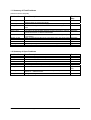
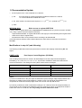
Microcontrollers
Errata Sheet
__________________________________________________________
V0.1 2004-06-04
Device
Stepping Code/Marking
Package
XC167CI-16F20F, -16F40F
EES-BA, ES-BA
P-TQFP-144-19
This Errata Sheet describes the deviations from the current user documentation.
The module oriented classification and numbering system uses an ascending sequence over several
derivatives, including already solved deviations. So gaps inside this enumeration can occur.
This Errata Sheet applies to all temperature (SAB-/SAF-/SAK-.....) and frequency versions (.20./.40.),
unless explicitly noted otherwise.
Current Documentation
• XC167-16 System Units - User's Manual V2.0, 2004-04
• XC167-16 Peripheral Units - User's Manual V2.0, 2004-04
• XC167CI Data Sheet - V1.1, 2003-06
• C166S V2 User's Manual (Core, Instruction Set) - V1.7, 2001-01
Note:
Devices additionally marked with EES- or ES- or E followed by a 3-digit date code are
engineering samples which may not be completely tested in all functional and electrical
characteristics, therefore they should be used for evaluation only.
The specific test conditions for EES and ES are documented in a separate Status Sheet.
Contents
Section
1. History List/Change Summary
2. Functional Problems
3. Deviations from Electrical- and Timing Specification
4. Application Hints
5. Documentation Update
Errata Sheet XC167CI-16F20F/40F (E)ES-BA
- 1 of 21 –
Mh/Es/UK, V0.1 2004-06-04
1. History List/Change Summary
from Errata Sheet Rev. 0.2 for XC167CI-16F20F/-16F40F devices with marking ES-AD, AD to this
Errata Sheet Rev. 0.1 for XC167CI-16F20F/-16F40F devices with marking EES-BA, ES-BA:
Documentation Reference updated:
- XC161 User's Manual V2.2, (Volume 1: System Units, Volume 2: Peripheral Units) - 2004-01
The following problems have been fixed:
-
CC6_X.002 (T12 Shadow Transfer for Phase Delay Function)
ADC_X.003 (Coincidence of Result Read and End of next Conversion or Start of Injected
Conversion in Wait for Read Mode)
ADC_X.004 (ADC Overrun Error Generation when result is read during last cycle of conversion)
TwinCAN2.005 (Double Send)
TwinCAN2.006 (CPUUPD fast set/reset)
SLEEP_X.001 (Wake up trigger during last clock cycle before entry into sleep mode)
OCDS_X.001 (BRKOUT# pulsing after Instruction Pointer Debug Event)
TAP_X.85 (Maximum ambient temperature during flash programming 85°C)
Description of the following problems included:
-
TwinCAN2.009 (CPUUPD remote)
FLASH_X.004 (PACER trap after wake-up from Sleep/Idle mode)
SCU_X.010 (Reset while PLL is not locked)
The following Application Hints have been added or modified:
-
SLEEP_X.H3.2 (Clock system after wake-up from Sleep Mode), replaces SLEEP_X.H3
IIC_X.H2 (Timing of Bit IRQD)
POWER_X.H1.1 (Initialization of SYSCON3 for Power Saving Modes), replaces POWER_X.H1
POWER_X.H2.2 (Power Consumption during Clock System Configuration), replaces
POWER_X.H2.1
SCU_X.H5 (Sleep/Idle/Power Down Mode not entered while PLLODIV = 0Fh)
The following Application Hints have been removed (covered by improved versions of the standard
documentation or other application hints):
-
BSL_X.H1.1 (Using the Bootstrap Loader over a Single-Wire Connection)
SLEEP_X.H1 (Sleep Mode during PLL Reconfiguration)
TwinCAN_X.H1 (Minimum fCAN for TwinCAN module)
ADC_X.H2 (Handling of Results of Injected Conversions by the A/D Converter)
CC6_X.H1 (CAPCOM6 Suspend Mode Entry and Exit ) [module redesigned]
The following text modules have been added in section ‘Documentation Update’:
-
RSTLEN
RSTLEN+1
duration of internal reset sequence: tRST = (2
) /tWDT (instead of (2
) /tWDT
SCU_X.D5 (VCO band after hardware/watchdog reset in single chip mode), replaces SCU_X.D4
Errata Sheet XC167CI-16F20F/40F (E)ES-BA
- 2 of 21 –
Mh/Es/UK, V0.1 2004-06-04
1.1 Summary of Fixed Problems
(reference: device step AB)
Problem Name
Short Description
Fixed in
Step
PORTS_X.009.1
Pins associated with External Bus Controller are driven after
Software Reset in Single-Chip Mode
Sleep and Power Down Mode Supply Current influenced by P3.5
Reset value of register FOCON after Software/Watchdog Timer
reset
T12 Shadow Transfer for Phase Delay Function
Coincidence of Result Read and End of next Conversion or Start of
Injected Conversion in Wait for Read Mode
ADC Overrun Error Generation when result is read during last cycle
of conversion
Wake up trigger during last clock cycle before entry into sleep mode
Double Send
CPUUPD fast set/reset
BRKOUT# pulsing after Instruction Pointer Debug Event
Maximum ambient temperature during flash programming 85°C
ES-AC
PORTS_X.010
SCU_X.007
CC6_X.002
ADC_X.003
ADC_X.004
SLEEP_X.001
TwinCAN2.005
TwinCAN2.006
OCDS_X.001
TAP_X.85
ES-AC
ES-AC
(E)ES-BA
(E)ES-BA
(E)ES-BA
(E)ES-BA
(E)ES-BA
(E)ES-BA
(E)ES-BA
(E)ES-BA
1.2 Summary of Open Problems
Problem Name
Short Description
EBC_X.003
CPU_X.002
TwinCAN2.007
TwinCAN2.008
TwinCAN2.009
FLASH_X.004
SCU_X.010
TwinCAN access with EBC enabled
Branch to wrong target after mispredicted JMPI
Transmit after error
Double remote request
CPUUPD remote
PACER trap after wake-up from Sleep/Idle mode
Reset while PLL is not locked
OCDS_X.002
OCDS indicates incorrect status after break_now requests if
PSW.ILVL ≥ CMCTR.LEVEL
Wrong MAC Flags are declared valid at Core - OCE interface
OCE_X.001
Errata Sheet XC167CI-16F20F/40F (E)ES-BA
Remarks
- 3 of 21 –
steps ≥ BA
steps ≥ BA
(E)ES-BA
only
Mh/Es/UK, V0.1 2004-06-04
1.3 Summary of Application Hints
Name
Short Description
CPU_X.H1
CPU_X.H2
FLASH_X.H1.1
FLASH_X.H2.1
Configuration of Registers CPUCON1 and CPUCON2
Special Characteristics of I/O Areas
Access to Flash Module after Program/Erase
Access to Flash Module after Wake-Up from Sleep/Idle Mode or
Shut-Down
Read Access to internal Flash Module with modified Margin Level
Minimum active time after wake-up from sleep or idle mode
Clock system after wake-up from Sleep Mode
Entering Idle Mode after Flash Program/Erase
Polling of Bit ADBSY
Break on MUL/DIV followed by zero-cycle jump
Maximum IIC Bus Data Rate at low fCPU
Timing of Bit IRQD
Initialization of SYSCON3 for Power Saving Modes
Power Consumption during Clock System Configuration
RSTOUT# driven by weak driver during HW Reset
Shutdown handshake by software reset (SRST) instruction
Preservation of internal RAM contents after reset
Effect of PLLODIV on Duty Cycle of CLKOUT
Changing PLLCON in Emergency Mode
Resetting and Disabling of the Real Time Clock
Read Access to register FOCON
FLASH_X.H3.1
FLASH_X.H4
SLEEP_X.H3.2
IDLE_X.H1
ADC_X.H1
BREAK_X.H1
IIC_X.H1
IIC_X.H2
POWER_X.H1.1
POWER_X.H2.2
RSTOUT_X.H1
SCU_X.H1
SCU_X.H2.1
SCU_X.H3
SCU_X.H4
RTC_X.H1.1
FOCON_X.H1
Errata Sheet XC167CI-16F20F/40F (E)ES-BA
Remarks
- 4 of 21 –
steps ≥ AC
steps ≥ AC
steps ≥ BA
steps ≥ AD
Mh/Es/UK, V0.1 2004-06-04
2. Functional Problems
EBC_X.003:
TwinCAN Access with EBC enabled
If the External Bus Controller (EBC) is enabled, a read or write access to the TwinCAN module fails
when an external bus access with TCONCSx.PHA ≠ 00b precedes the TwinCAN access.
Workaround:
Since it is hard to predict the order of external bus and TwinCAN accesses (in particular when PEC
transfers are involved), it is recommended to set bitfield PHA to '00' in all TCONCSx registers which
are used for external bus accesses.
CPU_X.002:
Branch to wrong target after mispredicted JMPI
After a JMPI is initially mispredicted according to the static branch prediction scheme of the C166S V2,
code execution may continue at a wrong target address in the following situations:
Situation I:
a memory write operation is processed by the DMU
followed by a MUL(U)
followed by the mispredicted JMPI
Example_1:
MOV mem, [Rwn]
MUL R13, R14
JMPI cc_NV, [R6]
Situation II:
MUL(U) or DIV(L/U/LU)
followed by not-mispredicted zero-cycle jump (e.g. JMPA, JMPR, JMPS; bit CPUCON1.ZCJ = 1)
followed by the mispredicted JMPI
-
Example_2a:
MULU R13, R14
JMPA- cc_V, _some_target
JMPI cc_NV, [R6]
; predicated not taken => correct
; taken, but predicted not taken
It could be possible that the JMPI is at the jump target of the JMPA, if it is taken:
Example_2b:
MULU R13, R14
JMPA+ cc_NZ, _jmpi_addr
..... other code ....
_jmpi_addr: JMPI cc_NV, [R6]
; predicted taken => correct
; taken but predicted not taken
Effect on tools:
In the Altium/Tasking compiler (v7.0 and above) the problem is not present. The result of a MUL/DIV
instruction is available through the MDL/MDH SFRs. These SFRs are not allocatable by the register
allocator. Therefore, the compiler always needs a MOV instruction to transfer MDL/H to a GPR. This
avoids the problem.
In the RT- and FP-libraries (v7.0 and above) the problem was not found. Versions lower than v7.0 do
not explicitly support the C166S V2 core.
Errata Sheet XC167CI-16F20F/40F (E)ES-BA
- 5 of 21 –
Mh/Es/UK, V0.1 2004-06-04
In case optimizations are implemented in future versions which could cause this problem to occur, also
a workaround will be included.
All Keil C166 tool Versions (compiler and libraries) since V3.xx do not generate a MUL(U) or a
DIV(L/U/LU) followed by either of the jump instructions JMPR, JMPS, JMPA, JMPI. Basically the
support of the C166S V2 core requires anyway V4.21 or higher.
Workarounds (e.g. for program parts written in assembly language):
-
generally disable overrun of pipeline bubbles by clearing bit CPUCON2.OVRUN (CPUCON2.4 =
0). This will result only in a negligible performance decrease, and will prohibit corruption of the
target IP of the JMPI.
or:
- provide a NOP (or any other suitable instruction) between the MUL/DIV instructions and the
succeeding jump in the above cases. To simplify, place a NOP between any MUL/DIV and a
JMPR, JMPS, JMPA, JMPI that might follow it. Other branches (CALLs, jump-on-bit instructions)
do not need to be taken into account.
TwinCAN2.007:
Transmit after Error
During a CAN error, transmission may stop (after EOF or an error frame), until a successful reception
or a write access to the TwinCAN module.
Detailed Description
In case of a CAN error and there is no other activity on the CAN module (e.g. frame reception / frame
transmission on the other CAN node / write access to any CAN register), the transmission of
messages may stop, even if some transmit requests are still set.
The CAN module will start transmitting immediately, after a reception or a write access to the module.
Workarounds
a)
Write periodically 0xFFFF to one of the MSGCTRx registers, as this value is having no effect on
the register.
b)
In case writing to a CAN register shall be the exception, use the last error code (LEC) interrupt.
This shall start writing to one of the MSGCTRx register 0xFFFF, in case the LEC value is unequal
to 0.
TwinCAN2.008:
Double remote request
After the transmission of the remote request, TXRQ is not cleared in the receive object, if NEWDAT is
set. As a consequence the remote request is transmitted once again.
Workaround:
Clear NEWDAT after the reception of a data frame.
TwinCAN2.009:
CPUUPD remote
In case of a remote request to a standard message object which is chosen for transmission, a transmit
of the data frame takes place, even if CPUUPD is currently set.
Detailed Description
If a transmit message object gets a remote request and there is no other message object with higher
transmit priority pending for transmission, then the transmit object sends the data frame to answer the
remote request, even if CPUUPD is set.
Errata Sheet XC167CI-16F20F/40F (E)ES-BA
- 6 of 21 –
Mh/Es/UK, V0.1 2004-06-04
Workaround
This workaround is only required in systems where remote requests are used.
To answer remote requests, the MMC bitfield in MSGFGCR has to be configured to a FIFO slave
object instead of a standard message object for transmission. To reach this goal, the following settings
for the corresponding message object are needed:
•
MSGFGCRn.MMC := (011)b FIFO slave object
•
MSGFGCRn.CANPTR := n shall reference itself, by referring to the message object number of
this object.
•
MSGFGCRn.FD := 0
FLASH_X.004
PACER Trap after Wake-Up from Sleep/Idle Mode
An unexpected Program Access Error Trap (flag PACER = 1 in register TFR) occurs after a wake-up
event from sleep or idle mode under the following conditions:
-
bit field PFCFG = 01b in register SYSCON1, i.e. the flash module is switched off during sleep or
idle mode
-
a wake-up event (interrupt, PEC transfer, NMI#) occurs in a specific time window (few clock
cycles) after execution of the IDLE instruction during the flash deactivation process
-
and the corresponding interrupt/trap routine or the instruction following IDLE (in case interrupts are
disabled) or the PEC source data are located in the internal flash.
Workaround 1
Do not switch off the flash module in sleep or idle mode, i.e. leave bit field PFCFG = 00b in register
SYSCON1 (default after reset). This increases power consumption to a certain extent while reducing
the time overhead for sleep/idle mode entry and exit (in clocking modes where the clock is derived
from the VCO).
Workaround 2
In order to avoid the problem (when PFCFG = 01), make sure that the wake-up trigger only occurs
after the device has completely entered sleep or idle mode.
If the RTC is used as wake-up source, check e.g. the RTC before entering sleep mode. If the wake-up
trigger will occur soon, either skip entry into sleep mode, or extend the time for the next wake-up. If the
RTC time interval is reprogrammed, make sure that no interrupt occurs between reprogramming and
entry into sleep mode.
Workaround 3
In order to differentiate an unexpected PACER trap due to a wake-up trigger in the critical time window
from other events that can lead to a PACER trap, set a semaphore bit before executing the IDLE
instruction., e.g.
ATOMIC #2
BSET sema_idle
IDLE
In the trap handler for the PACER trap, if the semaphore bit is set and no other indications for the
PACER trap are found (e.g. error flags in register FSR are set), clear the semaphore bit and the
PACER flag and return from the trap handler with RETI. The stack contains a valid return address in
this case (e.g. address of instruction following IDLE in case interrupts were disabled during wake-up).
For PEC transfers during sleep or idle mode, which will cause a PACER trap if they read data from
flash, automatic return to sleep/idle mode is not accomplished with the concept described so far.
Errata Sheet XC167CI-16F20F/40F (E)ES-BA
- 7 of 21 –
Mh/Es/UK, V0.1 2004-06-04
In order to support return to idle/sleep mode after a PEC transfer (which is performed after the
RETI instruction from the PACER trap routine is executed), e.g. a semaphore bit may be used.
This bit may be set to ‘1’ before the IDLE instruction is executed. All trap (except PACER) and
interrupt service routines invoked after wake up from idle/sleep should clear this bit to ‘0’. After
having returned from the PACER trap routine to the program in the internal flash, this bit should
be tested (allow a sufficient time of e.g. 12 cycles for interrupt arbitration), and if it is still at ‘1’
(i.e. no interrupts/traps have occurred), repeat the IDLE instruction for re-entry into idle/sleep
mode.
Workaround 4
Use an auxiliary sequence in internal PRAM that bridges the time until the flash is ready after wake-up
from sleep/idle mode, e.g.:
-
Disable interrupts, and execute the IDLE instruction to enter sleep mode from the internal PRAM.
After wake-up, the instruction following IDLE will be executed (if no hardware trap or NMI# has
occurred).
-
Wait until the internal flash is ready after wake-up (check register FSR) before reading from the
internal flash). If the sequence in internal PRAM that includes the IDLE instruction is not CALLed
from internal flash (i.e. it is not terminated with a RETx instruction), at least 8 instructions that do
not read from the internal flash should be inserted after the IDLE instruction to avoid speculative
prefetches
-
Enable the interrupt system again.
The following details should be considered:
-
If hardware traps (including NMI#) can occur, add the corresponding interrupt vectors to PRAM
and modify register VECSEG to point to the PRAM space.
-
In order to support return to idle/sleep mode after a PEC transfer, e.g. a semaphore bit may be
used. This bit may be set to ‘1’ before the IDLE instruction is executed. All trap and interrupt
service routines invoked after wake up from idle/sleep should clear this bit to ‘0’. After having
returned to the program in the internal flash and having enabled the interrupt system, this bit
should be tested (allow a sufficient time of e.g. 12 cycles for interrupt arbitration), and if it is still at
‘1’ (i.e. no interrupts/traps have occurred), repeat the auxiliary routine that prepares for re-entry into
idle/sleep mode.
SCU_X.010
Reset while PLL is not locked
Under the conditions described below where the PLL is configured in a way such that it can not lock,
execution of the user program will not start after a software/watchdog timer reset, or after a hardware
reset with pin EA# = low, respectively. Instead, the device will remain in the reset state.
The problem occurs in PLL mode (PLLCTRL = 11b),
a) when PLLCON has been written by the user software with a configuration where the PLL can
not lock (e.g. PLLCON = 618Eh, fvco not within selected VCO band), and a software or watchdog
timer reset occurs, independent of the status of pin EA#.
b) when the PORT0 configuration selects a PLL configuration where the PLL can not lock (e.g.
mismatch between fosc and CLKCFG), and a hardware reset is executed with pin EA# = low
(external start).
This problem does not occur after a hardware reset (rising edge on RSTIN#) with EA# = high (start
from internal flash).
Errata Sheet XC167CI-16F20F/40F (E)ES-BA
- 8 of 21 –
Mh/Es/UK, V0.1 2004-06-04
Workarounds:
For case a):
- Do not write a configuration to PLLCON where the PLL can not lock.
Or
- Do not perform a software reset (instruction SRST) while PLLWRI = 1 and the PLL is in a state
where it can not lock. In this case, change PLLCON e.g. to direct drive mode (PLLCTL = 00)
before executing SRST.
- Disable the watchdog timer while the PLL is not running in the locked state and PLLWRI = 1.
For case b):
- Always select a PORT0 configuration where the PLL can lock when performing a hardware reset.
Errata Sheet XC167CI-16F20F/40F (E)ES-BA
- 9 of 21 –
Mh/Es/UK, V0.1 2004-06-04
Items in OCDS and OCE Modules
The following issues have been found in the OCDS and OCE modules. Please see the debugger or
emulator manufacturer's documentation whether or not these issues actually cause a problem or
restriction when the respective tool is used
OCDS_X.002:
OCDS indicates incorrect status after break_now requests if
PSW.ILVL ≥ CMCTR.LEVEL
When the OCDS processes a break_now request while the CPU priority level (in PSW.ILVL) is not
lower than the OCDS break level (in CMCTR.LEVEL), the actual break is delayed until either
PSW.ILVL or CMCTR.LEVEL is reprogrammed such that CMCTR.LEVEL > PSW.ILVL. If in the
meantime further debug events have occurred, register DBGSR will still indicate the status of the first
break_now request. If e.g. a software break is executed, the OCDS will accept this, but register
DBGSR will indicate the wrong cause of break.
Workarounds:
1. If the application uses tasks with different levels and debugging is to take place using the OCDS
break level feature (e.g. only tasks up to a maximum level are halted, higher-level tasks aren't halted,
and the OCDS level is programmed in between), there is no problem if:
- only classic hardware breakpoints (IP address) or software breakpoints are used (i.e. no trigger on
address, data, TASKID)
- no external pin assertions are used to trigger breaks
- no direct writes to DBGSR.DEBUG_STATE are used to force breaks
2. If break_now request sources are to be used, the maximum level of the application (PSW.ILVL)
should always be lower than the programmed OCDS break level (e.g. PSW.ILVL ≤ 14d,
CMCTR.LEVEL = 15d). This means that all generated break_now requests by the OCDS will always
be accepted, independent of the CPU / interrupt priority.
OCE_X.001:
Wrong MAC Flags are declared valid at Core - OCE interface
In case a MAC instruction (Co...) is directly followed by a MOV MSW, #data16 instruction, the upper
byte of data16 is output instead of the flags corresponding to the MAC instruction. The bug was found
with code:
coshr #00001h
mov MSW, #00100h
(+ other variations of data16)
Workaround:
Add a NOP between the two instructions:
coshr #00001h
nop
mov MSW, #00100h
(+ other variations of data16)
Errata Sheet XC167CI-16F20F/40F (E)ES-BA
- 10 of 21 –
Mh/Es/UK, V0.1 2004-06-04
3. Deviations from Electrical and Timing Specification
Reference: XC167CI Data Sheet - V1.1, 2003-06 (see also Status Sheet)
The following restrictions should be considered:
No deviations from this specification are known.
Symbol
-
Parameter
-
Value
-
Final values of timing deviations from AC specifications will be documented after characterization.
4. Application Hints
CPU_X.H1
Configuration of Registers CPUCON1 and CPUCON2
The default values of registers CPUCON1 and CPUCON2 have been chosen to provide optimized
performance directly after reset. It is recommended
- not to modify the performance related parts of register CPUCON1
- not to modify register CPUCON2, except for test purposes or for enabling specific workarounds
under special conditions (see e.g. problem CPU_X.002 or application hint BREAK_X.H1).
CPUCON2:
reset/recommended value = 8FBBh
CPUCON1:
reset/recommended value = 0..0 0XXX X111; only the 3 lsbs are performance related
Bit Position
Field
Name
CPUCON1.[15:7] 0
CPUCON1.[6:5] VECSC
Value Description
0
00
CPUCON1.4
WDTCTL
0
CPUCON1.3
SGTDIS
0
CPUCON1.2
CPUCON1.1
CPUCON1.0
INTSCXT
BP
ZCJ
1
1
1
CPU_X.H2
; enables several performance features
reserved
scaling factor for vector table, value depends on application,
'00' is compatible to C166 systems
configuration for scope and function of DISWDT/ENWDT
instructions, value depends on application, '0' is compatible
to C166 systems
segmentation enable/disable control, value depends on
application
enable interruptibility of switch context
enable branch prediction unit
enable zero cycle jump function
Special Characteristics of I/O Areas
As an element of performance optimization, the pipeline of the C166S V2 core may perform
speculative read accesses under specific conditions. In case the prediction for the speculative read
was wrong, the read to the actually required location is restarted. While this method is uncritical e.g. for
accesses to non-volatile memories or SRAMs, it may cause problems on devices which do not tolerate
speculative reads (e.g. FIFOs which are advanced on every read access).
No speculative reads are performed in memory areas which are marked as I/O area. This memory
area includes
- the SFR and ESFR space (e.g. with buffers for received data from serial interfaces or A/D results)
- the 4 Kbyte internal I/O area (00'E000h..00'EFFFh), including IIC and SDLM module (on XC161)
- the 2 Mbyte external I/O area (20'0000h..3F'FFFFh), including the TwinCAN module (default: from
20'0000h .. 20'07FFh)
Errata Sheet XC167CI-16F20F/40F (E)ES-BA
- 11 of 21 –
Mh/Es/UK, V0.1 2004-06-04
It is therefore recommended to map devices which do not tolerate speculative reads into the 2 Mbyte
external I/O area (20'0000h..3F'FFFFh).
For further special properties of the I/O areas, see p.3-8 in the XC167 System Units User's Manual,
V1.1, 2002-12.
FLASH_X.H1.1
Access to Flash Module after Program/Erase
After the last instruction of a program or erase command, the BUSY bit in register FSR is set to '1'
(status = busy) after a delay of one instruction cycle. When polling the BUSY flag, one NOP or other
instruction which is not evaluating the BUSY flag must be inserted after the last instruction of a
program or erase command.
No additional delay is required when performing the first operand read or instruction fetch access from
the flash module after the BUSY bit has returned to '0' (status = not busy).
FLASH_X.H2.1
Access to Flash Module after Wake-Up from Sleep/Idle Mode or
Shut-Down
In order to reduce power consumption, the devices of the XC166 family allow to selectively disable
individual modules. The flash module may be disabled upon entry into Idle or Sleep mode (selection in
register SYSCON1), and it will be automatically re-enabled after wake-up from idle/sleep. Like other
on-chip peripheral modules, the flash module may also be shut down/turned on by software (flexible
peripheral management via register SYSCON3) while not required during specific operating periods of
an application. Since the transition from active to inactive state (and vice versa) requires several clock
cycles, some special situations have to be considered when access to the flash is required directly
after wake-up:
If during entry into sleep or idle mode where the flash module shall be disabled (bit field PFCFG = 01b
in register SYSCON1),
-
a wake-up event (PEC, interrupt, NMI#) occurs before the flash deactivation process is complete,
and the corresponding PEC transfer or interrupt/trap routine wants to access operands or
instructions in the internal flash
then the flash access is automatically delayed until the flash is ready again.
When the flash is disabled by software (shut-down) by writing bit PFMDIS = 1 in register SYSCON3,
- and it is (at some later time) enabled again by writing PFMDIS = 0
- and the instruction immediately following the instruction which sets PFMDIS = 0 is fetched or reads
operands from internal flash
then the PACER flag in register TFR is set and the BTRAP routine is entered.
Therefore, it is recommended to insert 4 NOPs before the internal flash is accessed again after
PFMDIS has been set to 0.
FLASH_X.H3.1
Read Access to internal Flash Module with modified Margin Level
1. When the internal flash module is read (e.g. for test purposes) with bit field margin = 0001b (low
level margin) in register MAR, an additional wait state must be used, i.e.
- bit field WSFLASH in register IMBCTR must be set to 10b for fcpu > 20 MHz,
- bit field WSFLASH in register IMBCTR must be 01b (default after HW reset) for fcpu < 20 MHz
2. When writing to the Margin Control Register MAR (with the Write Margin command), bit MAR.7
must be written as ‘1’.
Errata Sheet XC167CI-16F20F/40F (E)ES-BA
- 12 of 21 –
Mh/Es/UK, V0.1 2004-06-04
FLASH_X.H4
Minimum active time after wake-up from sleep or idle mode
If the flash module is automatically disabled upon entry into sleep or idle mode (bit field PFCFG = 01b
in register SYSCON1), sleep or idle mode should not be re-entered before a minimum active (“awake”)
time has elapsed. Otherwise, the current consumption during this sleep/idle phase will be ~ 1 mA
above the specified limits of the Data Sheet. Therefore,
-
If code is executed from the internal flash after wake-up, at least 16 instructions should be
executed from the internal flash before re-entering sleep/idle mode.
-
If code is executed from external memory or PRAM, wait until the flash BUSY bit returns to ‘0’
before re-entering sleep/idle mode.
-
If PEC transfers with automatic return to sleep/idle mode shall be triggered by the wake-up event,
use e.g. the following procedure:
use an auxiliary routine in internal flash that waits until the flash is ready after wake-up from
sleep or idle mode, e.g.
- define a semaphore bit that is set to ‘1’ before the IDLE instruction is executed. All trap and
interrupt service routines invoked after wake up from idle/sleep should clear this bit to ‘0’
- disable interrupts
- execute the IDLE instruction
- if idle or sleep mode is terminated by an interrupt request, the instructions following the IDLE
instruction will be executed (the interrupt request flags remain set)
- if idle or sleep mode was terminated by an NMI#, the trap handler will be invoked
- enable interrupts to allow prioritization of requests for interrupt or PEC service
- the instructions following the IDLE instruction should test the flash BUSY bit in register FSR
when the flash is ready, and at least 12 instructions have been executed after the interrupt system has
been enabled, and if the semaphore bit is still at ‘1’ (i.e. no interrupts/traps have occurred), disable
interrupts and return to the IDLE instruction
SLEEP_X.H3.2
Clock system after wake-up from Sleep Mode
There are different wake-up behaviors, depending on the PLL control setting used in register PLLCON
during entry into sleep mode, and depending on whether the RTC is running on the main oscillator.
Note that in either case, the VCO is turned off during sleep mode, and does not contribute to any
additional power consumption.
•
In bypass mode with VCO off (PLLCTRL = 00b), the device will directly continue to run on the
frequency derived from the external oscillator input after wake-up from sleep. If the RTC is running
on the main oscillator, the device is immediately clocked, since the oscillator (input XTAL1) is not
turned off during sleep mode.
If the RTC was not running on the main oscillator, the system will not be clocked until the
amplitude on the external oscillator input XTAL1 exceeds the input hysteresis. This requires typ. a
few ms, depending on external crystal/oscillator circuit.
With this mode, there is no oscillator watchdog function, and the system will not be clocked until
the external oscillator input XTAL1 receives a clock that exceeds the input hysteresis.
•
In bypass mode with VCO on (PLLCTRL = 01b), the device will directly continue to run on the
frequency derived from the external oscillator input after wake-up from sleep if the RTC continues
to run on the main oscillator in sleep mode.
In case the PLL was locked before entry into sleep mode, emergency mode is entered. This
results in PLLODIV = 0Fh and bit SYSSTAT.EM = 1. This change of configuration will not be
notified by the PLL Unlock/OWD interrupt (flag PLLIR). This condition will remain until an
external HW reset is applied, or a wake-up event from sleep mode with main oscillator off (i.e.
RTC not running on main oscillator) occurs.
Errata Sheet XC167CI-16F20F/40F (E)ES-BA
- 13 of 21 –
Mh/Es/UK, V0.1 2004-06-04
If the RTC was not running on the main oscillator, (i.e. the main oscillator was off during sleep
mode), the device will wake-up using the internal PLL base frequency from the VCO (fbase/16) and
will temporarily stay in emergency mode (i.e. run on the frequency derived from the VCO) until bit
OSCLOCK in register SYSSTAT gets set to 1.
It is not possible to switch to direct drive (VCO bypass) mode within this timeframe. If bypass mode
(PLLCTRL = 00b) is required by an application after wake-up from sleep, it is therefore
recommended to switch to bypass mode already before entry into sleep mode (check PLLCON for
its target value before executing the IDLE instruction to enter sleep mode). See also SCU_X.H5.
•
In PLL mode with input clock from XTAL1 disconnected (PLLCTRL = 10b), the device will only
wake up from sleep if the RTC was not running on the main oscillator (i.e. when the main oscillator
is off during sleep mode). In this case, the device will run using the internal PLL base frequency
from the VCO (fbase/16) until the amplitude on the external oscillator input XTAL1 exceeds the input
hysteresis, and then switch to fbase/k with the output divider selected by PLLODIV.
If the RTC is running on the main oscillator, the device will not wake-up from sleep mode with this
PLLCTRL setting. It is therefore recommended to switch to bypass mode (PLLCTRL = 00b) before
entry into sleep mode (check PLLCON for its target value before executing the IDLE instruction to
enter sleep mode).
•
In PLL mode with input clock from XTAL1 connected to the VCO (PLLCTRL = 11b), if the RTC
was not running on the main oscillator, the device will wake-up in emergency mode and run using
the internal PLL base frequency from the VCO (fbase/16) until the amplitude on the external oscillator
input XTAL1 exceeds the input hysteresis. Then the PLL resynchronizes to the target frequency
determined by the settings in register PLLCON. When bit OSCLOCK gets set in register
SYSSTAT, the output divider PLLODIV will be set to the target value.
If the RTC is running on the main oscillator, the device will wake-up and resynchronize to the
target frequency determined by the settings in register PLLCON.
In case the PLL was locked before entry into sleep mode, emergency mode is entered. This
results in PLLODIV = 0Fh and bit SYSSTAT.EM = 1. This change of configuration will not be
notified by the PLL Unlock/OWD interrupt (flag PLLIR). This condition will remain until an
external HW reset is applied, or a wake-up event from sleep mode with main oscillator off (i.e.
RTC not running on main oscillator) occurs.
As an alternative, switch to bypass mode with VCO on and PLL unlocked before entering sleep
mode (e.g. PLLCON = 2000h). After wake-up, PLLCON may be reconfigured to the desired
PLL operating mode.
IDLE_X.H1
Entering Idle Mode after Flash Program/Erase
After a program/erase operation, idle mode should not be entered before the BUSY bit in register FSR
has returned to '0' (status = not busy).
ADC_X.H1
Polling of Bit ADBSY
After an A/D conversion is started (standard conversion by setting bit ADST = 1, injected conversion by
setting ADCRQ = 1), flag ADBSY is set 5 clock cycles later. When polling for the end of a conversion, it
is therefore recommended to check e.g. the interrupt request flags ADC_CIC_IR (for standard
conversions) or ADC_EIC_IR (for injected conversions) instead of ADBSY.
Errata Sheet XC167CI-16F20F/40F (E)ES-BA
- 14 of 21 –
Mh/Es/UK, V0.1 2004-06-04
BREAK_X.H1
Break on MUL/DIV followed by zero-cycle jump
When a MUL or DIV instruction is immediately followed by a falsely predicted conditional zero-cycle
jump (JMPR or JMPA on any condition other than cc_UC),
and
- either a 'break now' request is set at the time the MUL / DIV instruction is being executed (i.e. a
break request on operand address, data, task ID, BRKIN# pin etc. is generated by one of the
instructions (may be up to four) preceding MUL/DIV)
- or a 'break-before-make' request (break on IP address) is derived from the instruction immediately
following the jump (jump target or linear following address, depending whether the jump is taken or
not )
then the internal program counter will be corrupted (equal to last value before jump), which will lead to
a false update of the IP with the next instruction modifying the IP.
This problem occurs for debugging with OCDS as well as with OCE.
Note:
The Tasking and Keil compilers (including libraries) do not generate this type of critical
instruction sequence.
Workarounds (choices):
For assembler programmers, one of the following workarounds may be used
(1) disable zero-cycle operation for jumps when debugging code (set CPUCON1.ZCJ to '0'), or
(2) include a NOP after any MUL/DIV instruction followed by a conditional jump (JMPR, JMPA), or
(3) do not set any 'break-before-make'-type breakpoints on the instruction following the jump, or 'break
now'-type breakpoints shortly before or on the MUL / DIV instructions
IIC_X.H1
Maximum IIC Bus Data Rate at low fCPU
The extended IIC bus data rate of 400 Kbit/s can not be used for clock frequencies fCPU < 8 MHz.
When a lower CPU frequency is used system limitations (frequency accuracy and duty cycle of serial
clock SCL) have to be considered.
IIC_X.H2
Timing of Bit IRQD
The Data Transfer Event Interrupt Request Flag IRQD in register IIC_ST is set to ‘1’ after the
acknowledge bit of the last byte has been received or transmitted.
If bit IIC_CON.INT = 0, IRQD is automatically cleared to ‘0’ by HW with a delay of 1 module clock cycle
upon a complete read or write accesses to the buffers RTB0...3 (according to the buffer size defined
via bit field CI in register IIC_CON). Therefore, after reading/writing RTB0...3, either
-
add 5 NOPS, or
read status register IIC_ST twice
before evaluating the status of flag IRQD.
POWER_X.H1.1
Initialization of SYSCON3 for Power Saving Modes
For minimum power consumption during power saving modes, all modules which are not required
should be disabled in register SYSCON3, i.e. the corresponding disable bits should be set to '1',
including bits which are marked as 'reserved' (this provides compatibility with future devices, since all
SYSCON3 bits are disable bits). Reading these bits will return the written value, as for peripherals
without shut-down handshake. For peripherals equipped with peripheral shut-down handshake,
reading allows to check their shut-down status.
Errata Sheet XC167CI-16F20F/40F (E)ES-BA
- 15 of 21 –
Mh/Es/UK, V0.1 2004-06-04
POWER_X.H2.2
Power Consumption during Clock System Configuration
In the following situations
(1) after wake-up from sleep mode until oscillator lock
(2) after a clock failure (PLL unlock or oscillator fail) until clock reconfiguration by software
the device is internally clocked by the VCO running on the base frequency of the currently selected
VCO band divided by 16. This results in an operating frequency range of 1.25 .. 11.25 MHz, depending
on the currently selected VCO band.
Systems designed for lower target frequencies should consider the increased power consumption due
to the potential frequency increase during these phases of operation.
Exception in bypass mode with VCO off: in case (1), if the RTC is not running on the main oscillator,
and case in (2) the device stops until it again receives a clock from the oscillator.
RSTOUT_X.H1
RSTOUT# driven by weak driver during HW Reset
A weak driver (see specification in Data Sheet) has been implemented on pin RSTOUT# which is
driven low while RSTIN# is asserted low. After the end of the internal reset sequence, RSTOUT#
operates in default mode (strong driver/sharp edge mode, i.e. POCON20.PDM3N[15:12] = 0000b).
The software setting POCON20.PDM3N[15:12] = xx11b is not supported and should not be selected
by software, otherwise pin RSTOUT# floats.
SCU_X.H1
Shutdown handshake by software reset (SRST) instruction
In the pre-reset phase of the software reset instruction, the SCU requests a shutdown from the active
modules equipped with shutdown handshake (see Section 8.3.4 in User’s Manual, volume System
Units). The pre-reset phase is complete as soon as all modules acknowledge the shutdown state.
As a consequence, e.g. the A/D converter will only acknowledge the request after the current
conversion is finished (fixed channel single conversion mode), or after conversion of channel 0 (auto
scan single conversion mode). If the ‘wait for DAT read’ mode is selected (bit ADWR = 1), the ADC
does not acknowledge the request if the conversion result from register DAT has not been read.
Therefore, before the SRST instruction is executed, it is recommended e.g. in the continuous (fixed or
auto scan) conversion modes to switch to fixed channel single conversion mode (ADM = 00) and
perform one last conversion in order to stop the ADC in a defined way. In the auto scan conversion
modes, this switch is performed after conversion of channel 0. If a 0-to-1 transition is forced in the start
bit ADST by software, a new conversion is immediately started. If the ‘wait for DAT read’ mode is
selected, register DAT must be read after the last conversion is finished.
The external bus controller e.g. may not acknowledge a shutdown request if bus arbitration is enabled
and the HOLD# input is asserted low.
SCU_X.H2.1
Preservation of internal RAM contents after reset
After a power-up hardware reset the RAM contents are undefined.
The contents of the on-chip RAM modules are preserved during a software reset or a watchdog timer
reset.
Because a hardware reset can occur asynchronously to internal operation, it may interrupt a current
write operation and so inadvertently corrupt the contents of on-chip RAM. RAM contents are preserved
if the hardware reset occurs during Power-Down mode, during Sleep mode, or during Idle mode with
no PEC transfers enabled.
Errata Sheet XC167CI-16F20F/40F (E)ES-BA
- 16 of 21 –
Mh/Es/UK, V0.1 2004-06-04
After any reset, RAM locations in the following area are used by the internal start-up code and will
therefore be overwritten:
0FBA0h … 0FC1Fh
Programs that e.g. perform RAM checksum calculations after reset should exclude this memory area.
SCU_X.H3
Effect of PLLODIV on Duty Cycle of CLKOUT
When using even values (0..14) for the output divider PLLODIV in register PLLCON, the duty cycle for
signal CLKOUT may be below its nominal value of 50%. This should only be a problem for applications
that use both the rising and the falling edge of signal CLKOUT.
When using odd values (1..15) for PLLODIV, where PLLODIV = 15 (0Fh) is selected by hardware only
during clock system emergency mode or reconfiguration, the duty cycle for signal CLKOUT is on its
nominal value of 50%
PLLODIV
Duty
Cycle [%]
SCU_X.H4
0
45
2
33.33
4
40
6
42.86
8
44.44
10
45.45
12
46.13
14
46.67
Changing PLLCON in emergency mode
While the clock system is in emergency mode (e.g. after wake-up from sleep, or due to an external
clock failure), the clock output divider is set to 16, i.e. PLLODIV = 0Fh in register PLLCON. Emergency
mode is terminated if the internal oscillator lock counter has received 2048 clock ticks from XTAL1.
If PLLCON is written in emergency mode, all settings except bypass modes (PLLCTRL = 0Xb) become
effective immediately within a few clock cycles. As long as the system clock is still derived from the
VCO, and if a relatively small value k is written to PLLODIV, this results in the system running on an
internal frequency of fvco/k that may exceed the specified frequency limit for the device.
In general, it is recommended to wait until PLLODIV < 0Fh before PLLCON is written. Use a timeout
limit in case a permanent clock failure is present.
SCU_X.H5
Sleep/Idle/Power Down Mode not entered while PLLODIV = 0Fh
While the clock system is in reconfiguration (e.g. after write to PLLCON, or after wake-up from sleep
when an oscillator lock event occurs, or during transition to emergency mode after clock failure), entry
into power saving modes is delayed. If e.g. the IDLE instruction to enter sleep mode is executed in this
state, the peripherals are already stopped, and the CPU goes into hold state, but the internal clock
system will not be switched off until the reconfiguration is complete.
Unless it is guaranteed that the clock system will become stable after a reconfiguration, it is
recommended to wait until the clock system is stable (i.e. check for PLLODIV < 0Fh, use a timeout limit
in case a permanent clock failure is present) before executing the IDLE or PWRDN instruction to enter
the respective power saving mode.
Errata Sheet XC167CI-16F20F/40F (E)ES-BA
- 17 of 21 –
Mh/Es/UK, V0.1 2004-06-04
FOCON_X.H1
Read access to register FOCON
Bit FOTL and bit field FOCNT in register FOCON are marked as ‘rh’ in the User’s Manual, i.e. they can
not be modified by software. If register FOCON is read directly after it was written, the value read back
from the positions of FOTL and FOCNT represents the value that was written by the preceding
instruction, but not the actual contents of FOTL and FOCNT. In order to obtain correct values for FOTL
and FOCNT, either insert one NOP or other instruction that does not write to FOCON, or read FOCON
twice and discard the first result.
RTC_X.H1.1 Resetting and Disabling of the Real Time Clock
The clock source for the RTC can be selected by software via bit REFCLK (bit position RTC_CON.4)
REFCLK = 0: RTC count clock signal is fOSCaux (input XTAL3)
REFCLK = 1: RTC count clock signal is fOSCmain / 32 (input XTAL1)
Register RTC_CON is not affected by a hardware/software/watchdog reset. After power-up, it is
undefined. A reset of the RTC module is achieved by setting bit SYSCON0.15/RTCRST = 1. This way,
register RTC_CON is set to 8003h (RTC runs, prescaler by 8 enabled, bit REFCLK = 0).
The RTC clocking mode (synchronous, asynchronous) is determined by bit SYSCON0.14/RTCCM.
Note that register SYSCON0 is not affected by a software or watchdog reset. This means that when a
software or watchdog reset occurred while the RTC module was in asynchronous mode (selected by
bit SYSCON0.14/RTCCM = 1), it will return to asynchronous mode after a RTC reset triggered by
setting bit SYSCON0.15/RTCRST = 1 with a bit instruction.
For a software or watchdog reset that is followed by an initialization of the RTC module, it is
recommended to
- select synchronous RTC clocking mode, i.e. clear bit SYSCON0.14/RTCCM = 0
- reset the RTC module, i.e. set bit SYSCON0.15/RTCRST = 1.
This may be achieved with one word or bit field instruction, e.g.
EXTR #1
BFLDH SYSCON0, #0C0h, #80h
; RTCRST = 1, RTCCM = 0
wait_accpos: EXTR #1
JNB ACCPOS, wait_accpos
; wait until bit ACCPOS = 1
As a general recommendation, bit REFCLK should be set to the desired value after any start-up
(hardware, software, watchdog reset), and in particular whenever the RTC module is reset by setting
bit SYSCON0.15/RTCRST = 1.
When the RTC module is not used and shall be disabled after a (power-on) hardware reset, the
following steps are recommended:
1. reset the RTC by setting bit SYSCON0.15/RTCRST = 1
2. clear the RTC run bit by setting RTC_CON.0/RUN = 0
3. disable the RTC module by setting bit SYSCON3.14/RTCDIS = 1.
Errata Sheet XC167CI-16F20F/40F (E)ES-BA
- 18 of 21 –
Mh/Es/UK, V0.1 2004-06-04
5. Documentation Update
•
XC167 System Units –User's Manual V2.0, 2004-04:
-
p. 6-5:
-
p. 6-4, 6-25: duration of internal reset sequence: tRST = (2
-
p. 6-56:
the reset value for register SYSCON3 is 9FD0h as stated in the manual,
i.e. not all modules are enabled after reset.
RSTLEN
WDTCON_X.D1
RSTLEN+1
) /tWDT (instead of (2
) /tWDT
Write access to register WDTCON
A write access to register WDTCON in unprotected or secured mode (e.g. before execution of EINIT,
or by using a special command sequence) directly
- copies bit field WDTREL of register WDTCON to the high byte of the watchdog timer register WDT
- clears the low byte of register WDT,
- and selects the WDT clock prescaler factor according to bit field WDTIN.
This means that an effective write to WDTCON has the same effect as execution of instruction
SRVWDT.
Modifications in step AC (and following)
The following modifications have been performed on devices with stepping code/marking AC and
higher:
PORTS_X.D1
Port Output Control Registers (POCONz)
The encoding of the port driver modes in bit field PDMyN of the Port Output Control Registers
POCONz (y= 0..3, z=0L, 0H, 1L, 1H, 2..4, 6, 7, 9) has been modified for weak and medium driver
mode as listed below. The settings for strong driver mode remain unchanged.
Bit field POCONz.PDMyN
0011
0100
0101
0110
0111
Mode
Notes
weak driver
medium driver
medium driver
medium driver
reserved
1)
1)
1)
2)
Notes:
1) There is no difference in the port output characteristics (driver strength, edge shape) between the 3
selections for medium driver mode (PDMyN = 010Xb, 0110b). The electrical characteristics are
comparable to medium driver/sharp edge mode of the XC16x-16F step AB devices.
2) Currently, weak driver mode is selected for setting 0111b. However there will be approximately 30
µA (low level) to 80 µA (high level) additional current on Vddp per pin which is configured as output in
weak driver mode. To avoid this, use only setting 0011b for weak driver mode.
Errata Sheet XC167CI-16F20F/40F (E)ES-BA
- 19 of 21 –
Mh/Es/UK, V0.1 2004-06-04
Modifications in step AD (and future devices)
The following modifications have been performed on devices with stepping code/marking AD and
higher:
ADC_X.D2
A/D Converter Characteristics, Conversion Time
In order to increase accuracy, the conversion time with post calibration (default after reset) is extended
by 4tBC as follows:
resolution
with post calibration
without post calibration
8-bit
tC8 = 44tBC + tS+ 6tSYS
tC8 = 32tBC + tS+ 6tSYS
(2.75µs @ fBC = 20MHz)
(2.15µs @ fBC = 20MHz)
tC10 = 52tBC + tS+ 6tSYS
tC10 = 40tBC + tS+ 6tSYS
(3.15µs @ fBC = 20MHz)
(2.55µs @ fBC = 20MHz)
10-bit
Note:
(1) For time critical applications, post calibration may be disabled by software (set bit CALOFF = 1 in
register CTR0) after the reset calibration is finished (indicated by bit CAL = 0 in register CON1), and no
conversion is in progress (indicated by bit ADBSY = 0 in register CON). This is possible in enhanced
mode (bit MD = 1 in register CTR0) as well as in standard mode (MD = 0).
(2) The accuracy of the ADC depends to a great extent on the stability of the reference voltage VAREF, in
particular during the reset calibration phase.
(3) The ADC is currently tested with post calibration enabled. The accuracy with post calibration
disabled is guaranteed by design.
RTC_X.D2
Real Time Clock Source Selection
The clock source for the RTC can be selected by software via bit REFCLK (bit position RTC_CON.4)
REFCLK = 0: RTC count clock signal is fOSCaux (input XTAL3)
REFCLK = 1: RTC count clock signal is fOSCmain / 32 (input XTAL1)
Register RTC_CON is not affected by a hardware/software/watchdog reset. After power-up, it is
undefined. A reset of the RTC module is achieved by setting bit SYSCON0.15/RTCRST = 1. This way,
register RTC_CON is set to 8003h (RTC runs, prescaler by 8 enabled, synchronous mode, bit
REFCLK = 0). As a general recommendation, bit REFCLK should be set to the desired value after any
start-up (hardware, software, watchdog reset), and whenever the RTC module is reset by setting bit
SYSCON0.15/RTCRST = 1.
SCU_X.D1
Oscillator gain reduction
The gain of the main oscillator (pins XTAL1/2) may be reduced via software by setting bit SYSCON.12
(OSCGRED) = 1. After reset, high gain is selected by default to guarantee safe start-up.
The gain may be reduced when the oscillations have reached their full amplitude. For standard crystals
15
or ceramic resonators, this is typically 2 (32768) cycles of fXTAL1 after bit OSCLOCK = 1 (and, if the PLL
is used, PLLLOCK = 1) in register SYSSTAT. After reset, the internal reset sequence ensures that
OSCLOCK = 1 and PLLLOCK = 1 before the first instruction of the application software is executed,
unless a problem with the oscillator circuit is detected (in this case, flag PLLIR = 1).
Errata Sheet XC167CI-16F20F/40F (E)ES-BA
- 20 of 21 –
Mh/Es/UK, V0.1 2004-06-04
If the RTC is not running on the main oscillator during sleep mode (i.e. the main oscillator is off during
sleep mode), bit SYSCON.12 (OSCGRED) should be set to ‘0’ (high gain) before entry into sleep mode
to guarantee safe oscillator start-up after wake-up from sleep.
SCU_X.D2
Functionality of register OPSEN
When a breakpoint is hit, the on-chip peripherals selected in register OPSEN are stopped and placed
in power-down mode the same way as if disabled via register SYSCON3. Registers of peripherals
which are stopped this way can be read, but not written. A read access will not trigger any actions
within a disabled peripheral.
Application hint BREAK_X.H2 (Behavior of on-chip peripherals after Break) which was valid for step
AC and earlier steps is therefore removed for the Errata Sheet of step AD (and newer steps).
Note also the following documentation updates for some versions of the User’s Manual, volume
System Units:
Register Bit
Function
Device
SYSCON3.12
SYSCON3.10
SYSCON3.8
OPSEN.13
OPSEN.12
OPSEN.11
OPSEN.10
OPSEN.8
OPSEN.5
OPSEN.0
SDLMSEN
ASC1DIS
CC6DIS
CANSEN
SDLMSEN
I2CSEN
ASC1SEN
CC6SEN
PFLSEN
ADCSEN
XC161CJ-16F
all XC16x
XC164, XC167
all XC16x
XC161CJ-16F
XC161, XC167
all XC16x
XC164, XC167
all devices with program flash
all XC16x
It is recommended to leave bit OPSEN.5 (PFLSEN) at its default value ‘0’. Otherwise, the program
flash is deactivated when a breakpoint is hit (i.e. it can not be read), and it has to ramp up when
program execution is resumed (i.e. synchronization between software and peripherals is lost).
SCU_X.D3
Register PLLCON after software reset
Register PLLCON is not affected by a software reset, i.e. the current clock configuration remains
unchanged. PLLCON may be reconfigured by software, or an endless loop terminated by a watchdog
timer reset may be used to force PLLCON to its hardware reset value.
SCU_X.D5
VCO band after hardware/watchdog reset in single chip mode
From the falling edge of RSTIN# until 2048 stable oscillator clocks after the rising edge of RSTIN#,
always the lowest VCO band is selected (see POWER_X.H2). After that, for a hardware or watchdog
timer reset in single-chip mode, PLL bypass mode with the lowest VCO band is selected during the
internal reset phase (PLLCON = 2710h).
Product and Test Engineering Group, Munich
Errata Sheet XC167CI-16F20F/40F (E)ES-BA
- 21 of 21 –
Mh/Es/UK, V0.1 2004-06-04