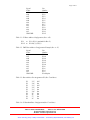
1
Artisan Technology Group is your source for quality new and certified-used/pre-owned equipment • FAST SHIPPING AND DELIVERY • TENS OF THOUSANDS OF IN-STOCK ITEMS • EQUIPMENT DEMOS • HUNDREDS OF MANUFACTURERS SUPPORTED • LEASING/MONTHLY RENTALS • ITAR CERTIFIED SECURE ASSET SOLUTIONS SERVICE CENTER REPAIRS Experienced engineers and technicians on staff at our full-service, in-house repair center WE BUY USED EQUIPMENT Sell your excess, underutilized, and idle used equipment We also offer credit for buy-backs and trade-ins www.artisantg.com/WeBuyEquipment InstraView REMOTE INSPECTION LOOKING FOR MORE INFORMATION? Visit us on the web at www.artisantg.com for more information on price quotations, drivers, technical specifications, manuals, and documentation SM Remotely inspect equipment before purchasing with our interactive website at www.instraview.com Contact us: (888) 88-SOURCE | [email protected] | www.artisantg.com User Manual AITG-VME Synchronizable Timecode Generator With VME Bus Interface Revision 1 Artisan Technology Group - Quality Instrumentation ... Guaranteed | (888) 88-SOURCE | www.artisantg.com Page 2 of 31 AITG-VME Synchronizable Timecode Generator with VME Bus Interface Operation & Maintenance Manual Revision 1 11209 Armour Drive El Paso, TX 79935 Toll Free Phone: 866.KSI.KSI3 Toll Free Fax: 866.593.2080 E-mail: [email protected] Website: www.ksi-corporation.com Artisan Technology Group - Quality Instrumentation ... Guaranteed | (888) 88-SOURCE | www.artisantg.com Page 3 of 31 Proprietary Notice This document contains data proprietary to DSPCon. However, permission is hereby granted by DSPCon to the purchaser and/or the purchaser’s subcontractor(s) and/or customer(s), to reproduce this Operation & Maintenance Manual, in whole or in part, for the purposes of installation, operation, maintenance, repair, backup, and/or training, subject to the following conditions: This page, in its entirety, shall be included in any reproduction; The information contained herein shall not be altered, publicly displayed, or disclosed to other vendors or representatives of vendors of similar equipment; Availability via a computer network shall be strictly limited to the purchaser, the purchaser’s subcontractor(s), and/or the purchaser’s customer(s). The software (if any) included with this product contains data proprietary to DSPCon. However, permission is hereby granted by DSPCon to the purchaser and/or the purchaser’s subcontractor(s) and/or customer(s), to copy the software diskette to another diskette, and/or to other media, and/or to a computer network, and to modify the software, in whole or in part, for the purposes of installation, operation, maintenance, repair, backup, and/or training, subject to the following conditions: The software shall not be publicly displayed or disclosed to other vendors or representative of vendors of similar equipment; Availability via a computer network shall be strictly limited to the purchaser, the purchaser’s subcontractor(s), and/or the purchaser’s customer(s). Receipt or possession of this document does not convey any rights to manufacture or reverse-engineer anything it may describe or imply, in whole or in part. Disclaimer This document reflects the specifications and features of the equipment that were current at the time of publication. DSPCon disclaims responsibility for any errors and/or omissions contained herein, and reserves the right to make changes to this manual and related equipment and software without notice or obligation. Software supplied with this product (if any) is for demonstration purposes only; it is not a full-featured program. The software media (diskette) is warranted to be readable when read in a computer using the proper operating system and proper disk drive. Software is neither warranted nor represented to be suitable for any particular application. THIS PRODUCT IS NOT AUTHORIZED FOR USE AS A CRITICAL COMPONENT IN LIFE SUPPORT DEVICES OR SYSTEMS WITHOUT THE EXPRESS WRITTEN CONSENT OF THE PRESIDENT OF DSPCON, INC. 11209 Armour Drive El Paso, TX 79935 Toll Free Phone: 866.KSI.KSI3 Toll Free Fax: 866.593.2080 E-mail: [email protected] Website: www.ksi-corporation.com Artisan Technology Group - Quality Instrumentation ... Guaranteed | (888) 88-SOURCE | www.artisantg.com Page 4 of 31 AITG-VME Revision History Revision 1 Revision Date 3/13/01 Modifications First revision for KSI, a division of DSPCon Inc. 11209 Armour Drive El Paso, TX 79935 Toll Free Phone: 866.KSI.KSI3 Toll Free Fax: 866.593.2080 E-mail: [email protected] Website: www.ksi-corporation.com Artisan Technology Group - Quality Instrumentation ... Guaranteed | (888) 88-SOURCE | www.artisantg.com Page 5 of 31 Table of Contents Proprietary Notice................................................................................................................. ...................................2 Disclaimer............................................................................................................................. ...................................2 Revision History ................................................................................................................... ...................................3 Table of Contents.................................................................................................................. ...................................4 Chapter 1—Introduction....................................................................................................... ...................................5 Chapter 2—Specifications .................................................................................................... ...................................8 2.1—Dimensions, Power, Fabrication & Temperature 2.2—VMEbus Interface 2.3—Inputs 2.4—Outputs 2.5—Indicators 2.6—Timing Chapter 3—Configuration .................................................................................................... ...................................12 3.1—General 3.2—Identifying Board Revision 3.3—Base Address Configuration 3.4—Address Modifiers on the VME Bus 3.5—Interrupt Request Level Configuration 3.6—VME Bus P2 Connector Configuration 3.7—P13 Pulse Output Trigger Configuration 3.8—W6, W7, W8 or P8 External/Internal Event Configuration 3.9—P14 FIFO Buffer Clear Configuration 3.10—P6 EEPROM Configuration Chapter 4—Pin Assignments................................................................................................ ...................................17 4.1—Test Points 4.2—Input/Output Pin Assignments Chapter 5—Installation..... ................................................................................................... ...................................20 Chapter 6—Programming. ................................................................................................... ...................................22 6.1—Determining Address Space 6.2—Reading Time 6.3—Interrupt Mode 6.4—Commands 6.5—Setting Propagation Delay Correction 6.6—Setting Time 6.7—External 1PPS Time Synchronization 6.8—Commands for Disabling and Re-enabling Code Input 6.9—Handlers and C Libraries Chapter 7—Preventative Maintenance ................................................................................. ...................................27 7.1—Oscillator Aging Adjustment 7.2—Rev D-E IRIG-B Output Adjustment 7.3—Rev F & Later IRIG-B Output Adjustment Chapter 8—In Case of Trouble............................................................................................. ...................................28 8.1—If your program has trouble talking to the AITG-VME 8.2—Bad data from FIFO port 8.3—Interrupt crashes 8.4—Board never syncs to input code or 1PPS 8.5—Before you cal l us Contact Information.......... ................................................................................................... ...................................30 11209 Armour Drive El Paso, TX 79935 Toll Free Phone: 866.KSI.KSI3 Toll Free Fax: 866.593.2080 E-mail: [email protected] Website: www.ksi-corporation.com Artisan Technology Group - Quality Instrumentation ... Guaranteed | (888) 88-SOURCE | www.artisantg.com Page 6 of 31 Chapter 1 – Introduction The AITG-VME is basically an accurate clock that automatically synchronizes to external time signals and whose time can be captured and read by the host VME bus computer. It is used in VME bus systems for time tagging, synchronizing multiple systems, and generating puts rates at exact times and exact frequencies. Optional operating system handlers can be used for user interface to the AITG-VME or users may directly access the AITG-VME with their own code (see appendices for sample code used in factory testing). Time capture can be caused by a logic pulse from the outside world (an "external" event) or can be caused by the host computer program (an "internal" event). The Z80 microcomputer in the AITG-VME transfers the captured time information (100s of days through units of microseconds- a total of 10 bytes) to the host by loading each of the 10 bytes sequentially into an on-board FIFO (first-in firstout) memory. The host program reads the 10 bytes sequentially from the FIFO through the AITG-VME VME bus interface. Handshaking is done by the host testing the OUTPUT READY bit of the AITGVME status register before each byte is read by the host from the FIFO output. The time required for the complete transfer is from 30 to 100 µS after the event occurs. It fluctuates because the on-board Z80 microcomputer may be interrupted while putting data in the FIFO. The time data is accurate to the exact microseconds when the event occurred and the accuracy is not affected by the transfer time. Users may configure the AITG-VME to interrupt the host VME processor when the first byte of data is loaded in the FIFO. In many cases, the interrupt handling (task switching) overhead exceeds the time required for the complete loading of the FIFO, so that the VME host may never actually need to wait for the microcomputer to complete loading the FIFO. Users will typically use internal events for software initiated time measurements and the external time stamp for intermittent and unpredictable events triggered by the outside world. The clock will automatically start counting at time 0 days through microseconds without any commands after power-on reset. To maintain synchronization with the outside world, the clock may be initialized and it's counting frequency adjusted (disciplined) to correct for any inherent errors due to adjustment, temperature change, or aging. The Z80 automatically performs these task, using as a reference input a standard modulated time code signal (IRIG-B, IRIG-A, NASA 36, XR3, or 2137) or optionally a precision 1 pulse per second from GPS (Global Positioning Satellite) system receiver. The clock time may also be set by commands from the host VME bus computer to the AITG-VME. The on-board clock is also used to generate an IRIG-B output time code signal that can be fed to other systems. If no input reference is available, the clock will count at its natural undisciplined frequency. If the input reference disappears after being initially present, the AITG-VME will continue counting from the current time, using the frequency discipline calculated while the reference was present. This is called "openloop" or "fly-wheel" operation. If the input reference reappears, the AITG-VME will determine its type and phase, and then use it for time and frequency reference. If the accumulated error during open loop operation doesn't exceed 200 µS, the time count will then continue unperturbed error during open loop term change in count frequency to cancel out the error) by the interruption. Else, an abrupt jump in time (called a "jam sync") will occur at the beginning of the next second. 11209 Armour Drive El Paso, TX 79935 Toll Free Phone: 866.KSI.KSI3 Toll Free Fax: 866.593.2080 E-mail: [email protected] Website: www.ksi-corporation.com Artisan Technology Group - Quality Instrumentation ... Guaranteed | (888) 88-SOURCE | www.artisantg.com Page 7 of 31 In VME bus standard terminology, the AITG-VME is an A16 (short supervisory or short non-privileged addressing) D08 (O) VME SLAVE. D16 transfers are also supported, but the high order byte is ignored. The user base address is configurable in 64 byte steps and the interrupt level of the on-board bus interrupter is configurable. Offset from the configured base address are bus interrupter control and vector registers, a status register, a command register, an internal event register, and a FIFO read register. The address of a given register in user address space is generated by adding the configured VME bus base address of the AITG-VME and the offset (6 bits) for the specific register. The 16-bit result is added to the host-specific 24 or 32 bit "A16 bus window" address. Status bits tell the host when event data is in the FIFO, when the input code signal is present, and when the clock is known to be in the time clock with the input time code or the 1PPS input. The time code signals encode "major" time (days, hours, minutes, and seconds) using pulsewidth and amplitude modulation onto a sign wave carrier waveform. The time code repeats once (IRIG-B, NASA 36, XR3, 2137) or ten times (IRIG-A) a second and includes reference marks to mark the exact beginning of a second or tenth of a second. Each repetition is called a frame, and the encoded time is the time at the reference mark at the beginning of the frame. The AITG-VME automatically determines the type of the input time code. The carrier frequency (10 KHz for IRIG-A, 1 KHz for IRIG-B, NASA36, 2137 and 250 Hz for XR3) is used by the AITG-VME during each frame for multiple high accuracy time comparisons between the input time code and the on-board clock. Because any single comparison has jitter, multiple measurements are averaged for an accurate result, which is then used by the Z80 for frequency disciplining. Because only about half of each frame is needed for time information, the remaining time is sometimes used to encode countdown information or other application specific information. Specialized firmware options for the AITG-VME can recover or generate this information. Depending on the actual absolute time accuracy required in the user's application, the AITG-VME may automatically correct for the time required for the time code signal to travel the distance between the time code source and the host computer. This delay time is called "propagation delay time" and is about 3.3 µS per kilometer for radio time code transmission and about 5 µS per kilometer for copper wire transmission. There is also a time delay on the order of 25 µS that may be caused by small phase shifts due to reactances at the time code input. To correct for propagation delay, the Z80 can use a propagation delay correction setting ranging between -1000 (because some time sources transmit early) and +8999 µS. The default setting is 0 µS after the AITG-VME is reset at power-on or after a RESET command from the user. Users can change the setting by a sequence of programmed commands to the command register on the AITG-VME. If absolute microseconds accuracy is required, the user will probably need to calibrate the AITG-VME when it is installed for propagation delay correction by comparing the on-board clock time with a portable reference (a 1 PPS GPS pulse is good for this). The correct propagation delay correction setting is converted on rapidly by trial and error. This setting will not need to be changed unless the location or cabling of the installation is changed. 11209 Armour Drive El Paso, TX 79935 Toll Free Phone: 866.KSI.KSI3 Toll Free Fax: 866.593.2080 E-mail: [email protected] Website: www.ksi-corporation.com Artisan Technology Group - Quality Instrumentation ... Guaranteed | (888) 88-SOURCE | www.artisantg.com Page 8 of 31 A 1 PPS reference input option allows a 1 pulse-per-second TTL pulse (usually from a GPS receiver) to be used for oscillator disciplining. AITG-VMEs configured for this option will use the code input for clock time set and disciplining if it is present, and automatically switch to the 1 PPS if the input code is not present. Because only minor time (fractions of a second) can be initialized form the 1 PPS; the AITGVME needs information from the user to set the days through seconds (major time). The user obtains this information from the GPS receiver (usually over a serial data link) and should then calculate what day, hour, minute, and second the next 1 PPS pulse will occur. This information should be formatted into a sequence of 9 data bytes (one per digit) followed by a SET NEXT 1 PPS TIME command. The user should send the 10-byte sequence to the AITG-VME command port at least once after the AITG-VME jam syncs to the 1 PPS signal. The loss-of-sync status bit will be asserted after the jam sync until the NEXT 1 PPS TIME SET commands are performed. If using 1 PPS input, the user can simply check the loss-of-synchronization bit periodically to see if the SET NEXT 1PPS TIME command sequence needs to be performed. If the user does not set major time, the AITG-VME will continue counting from the last major time (or 0 if starting from power-on reset). Inputs to the AITG-VME (via the J1 20 pin connector or the J6 BNC coaxial connector) are modulated time code (or 1PPS reference) and external event pulses up to 2000 events per second. Options allow external high stability oscillator input and GPS receiver time synchronization input. IRIG-B modulated time code and a range of 1 µS pulse width "on-time" TTL pulses are provided as outputs. Options include LED time displays and glavanically isolated transformer input. 11209 Armour Drive El Paso, TX 79935 Toll Free Phone: 866.KSI.KSI3 Toll Free Fax: 866.593.2080 E-mail: [email protected] Website: www.ksi-corporation.com Artisan Technology Group - Quality Instrumentation ... Guaranteed | (888) 88-SOURCE | www.artisantg.com Page 9 of 31 Chapter 2 – Specifications 2.1 Dimensions, Power, Fabrication, and Temperature Dimensions 261,75mm (10.30") height X 172.23mm (6.77") depth X 20mm (.788") width (VME 6U Single width Double height) Width (VME 6U Single width Double height) Power +5 VDC: (±5%) at 3.5A (max.(, + 12 VDC: (±5%) at 150mA (max.) - 12VDC: (±5%) at 100m A (max.) PWB Fabrication .062" thick FR4 fire-retardant glass-filed epoxy, two sided Temperature 0 to50 °C operating, -40 to 60 °C storage. 2.2 VMEbus Interface Data Type D08 (o) Slave, D16 Slave (even byte n/u) Addressing Type A16 (short supervisory address, short non-privileged address) Addressing Base A6 to A31 configurable by wire wrap Offset 1 - D08/D16 MC68153 control register 0 Offset 3 - D08/D16 MC68153 control register 1 Offset 5 - D08/D16 MC68153 control register 2 Offset 7 - D08/D16 MC68153 control register 3 Offset 9 - D08/D16 MC68153 vector register 0 Offset B - D08/D16 MC68153 vector register 1 Offset D - D08/D16 MC68153 vector register 2 Offset F - D08/D16 MC68153 vector register 3 Offset 11 - D08/D16 Command register Offset 13 - D08/D16 Internal event register Offset 15 - D08/D16 FIFO data read Offset 17 - Not used Offset 19 - D08/D16 Status register Status Bit 0: -"0" FIFO not empty, "1" FIFO empty Status Bit 1: -"0" input code amplitude <500mV pk/pk. "1" Input code amplitude >500mV pk/pk Status Bit 2: -"0" Synchronization error, "1" Good synchronization. 11209 Armour Drive El Paso, TX 79935 Toll Free Phone: 866.KSI.KSI3 Toll Free Fax: 866.593.2080 E-mail: [email protected] Website: www.ksi-corporation.com Artisan Technology Group - Quality Instrumentation ... Guaranteed | (888) 88-SOURCE | www.artisantg.com Page 10 of 31 The synchronization error is asserted until synchronization to input to <5µS is verified by the Z80 or when the observed time base error exceeds 5 µS for 5 successive observations spaced at 1second intervals. If the observed time base error exceeds 200 µS, jam resynchronization shall be initiated. Synchronization error is also asserted when input code is inconsistent or lost (unless 1PPS is present to verify time error). Status Bit (3-7): - Not used Offset (1B-1F): - Not used Event Spacing 200 µS minimum External Event Response Each external event causes 10 bytes of event time data to be stroked into FIFO Interrupt Vector The user programs the on-board MC68153 (BIM) with the desired vector. Interrupt Level One of IRQ1* to IRQ7* matching the level configured by P5 must be programmed into the MC68153 Bus Interrupter Module by the user if interrupts are used. 2.3 Inputs Event Spacing 200 µS minimum External Event Response Each external event causes 10 bytes of event time data to be stroked into FIFO Interrupt Vector The user programs the on-board MC68153 (BIM) with the desired vector. Interrupt Level One of IRQ1* to IRQ7* matching the level configured by P5 must be programmed into the MC68153 Bus Interrupter Module by the user if interrupts are used. Rev F and later do not require P5 configuration. Code input connector Configurable for 2 pins of 20 pin J1 connector, via P2 Backplane C rows, front panel isolated J6 BNC, or optional front panel SMB or SMC coaxial. Input Code Types Modulated IRIG-A, IRIG-B, NASA36, 2137, XR3. 11209 Armour Drive El Paso, TX 79935 Toll Free Phone: 866.KSI.KSI3 Toll Free Fax: 866.593.2080 E-mail: [email protected] Website: www.ksi-corporation.com Artisan Technology Group - Quality Instrumentation ... Guaranteed | (888) 88-SOURCE | www.artisantg.com Page 11 of 31 Input Code Configuration Automatic by Z80 firmware. Input Code Modulation Amplitude modulated. Ratio of large amplitude to small Amplitude cycles between 2:1 and 4:1 Input Code Amplitude 500 MV to 8V peak to peak. Input Code Frequency Error 100ppm maximum. Input Code Polarity Automatic reverse polarity detection and correction. Input Code Impedance >10KΩ allow parallel units to be driven by single code source. Input Common Mode Rejection (Rev A-C) Transformer for galvanic isolation. No XR3 support. Input Common Mode Rejection (Rev D and later) Balanced instrumentation amplifier input withstand ±200V common mode voltage. Option X substituted Transformer for galvanic isolation (deletes XR3 support). 1PPS GPS Time Sync (option M) Positive going TTL 100 µS max. Width front panel BNC input connector J5. IRIG-B output is only on J1 and P2. External Event Positive going TTL pulse. The user may select either connector J1 or (by configuring P11 & P12) the VME P2 connector for external event input. 2.4 Outputs Rates Two rates are selectable from 1 PPS, 5 PPS, 10 PPS, 20 PPS, 100 PPS, 1 KPPS, 10 KPPS, 50 KPPS, and 100 KPPS. The user may access these output signals on connector J1 or the VME P2 connector. IRIG-B 1KHZ amplitude modulate sine wave 3 V pk/pk 200Ω source impedance. 11209 Armour Drive El Paso, TX 79935 Toll Free Phone: 866.KSI.KSI3 Toll Free Fax: 866.593.2080 E-mail: [email protected] Website: www.ksi-corporation.com Artisan Technology Group - Quality Instrumentation ... Guaranteed | (888) 88-SOURCE | www.artisantg.com Page 12 of 31 2.5 Indicators Red LED Indicator lights when input code peak-to-peak amplitude <500-mV pk/pk. Green LED Indicator lights when time error between clock and input code (or 1 PPS) is <5 µS. Option D 9-digit (days through seconds) front panel .3" digit height Option D8 8-digit (hours through seconds) front panel .15" digit height. 2.6 Timing Resolution 1 µS Clock Range 1 µS through 366 days, 23 hours 59 minutes, 59.999999 seconds. Propagation Delay Correction Range -1000 µS through 8999 µS. Propagation Delay Setting From VME host using command sequence. Synchronization Time <20 seconds for<1µS error from power-on or change of Propagation delay setting. Open Loop Frequency Drift Open loop timing error shall not exceed 2 µS in 10 seconds after 60 minutes of operation with input code or 1 PPS at a constant temperature. 11209 Armour Drive El Paso, TX 79935 Toll Free Phone: 866.KSI.KSI3 Toll Free Fax: 866.593.2080 E-mail: [email protected] Website: www.ksi-corporation.com Artisan Technology Group - Quality Instrumentation ... Guaranteed | (888) 88-SOURCE | www.artisantg.com Page 13 of 31 Chapter 3 – Configuration 3.1 General The AITG-VME base VME bus address, VME bus interrupt level (rev A through rev E), rate outputs and external/internal event options are configured suing wire wrap or push-on jumpers. Input and Output connections to the VME P2 connector are also selected via header jumpers. The AITG-VME standard factory configured is described in following examples. Different (customer specified) custom configurations are not shown. Base VME Bus Address: A000 VME Bus Interrupt Level: IRQ5* (does not require configuration in Rev F and later) External/Internal Events: External selected (Rev A-B). Internal and External enabled (Rev C and later). FIFO HW Clear (Configurable in Rev C and later): Cleared by SYSRESET 3.2 Identifying Board Revision Because some configuration procedures vary according to revision level of the AITG-VME, the user should check Revision level before changing configuration. Rev A and B are unmarked with Revision level. Rev C, D, E is marked in component side copper etches near the handle next to U12. Rev F and later are marked in white lettering near U20. Because the same PWB module (with different firmware) is used for the VTTRVME time code translator product, the module may be marked AITG/VTTR-VME or AITG-VME/VTTRVME. 3.3 Base Address Configuration The AITG-VME base address in A16 (short) address space is configured by header P3. For Rev A to Rev E, table 3.1 shows, which address lines, correspond to pins on P3. Rev C through Rev E boards includes a pull-up network (RP2) which no longer requires any connections to P3-1. Rev F and later boards use push-on jumper configuration of P3 as shown in table 3.3. The P3 connector on Rev F and later are marked with address bits configuration without reference to the manual. Example (Rev A-E): If the AITG-VME A16 base address is to be A000, them the wire wrap jumper shown in Table 3.2 must be installed. Example (Rev F and later): If the AITG-VME A16 base address is to be A000 (standard factory configuration) then jumpers shown in Table 3.4 must be installed. 11209 Armour Drive El Paso, TX 79935 Toll Free Phone: 866.KSI.KSI3 Toll Free Fax: 866.593.2080 E-mail: [email protected] Website: www.ksi-corporation.com Artisan Technology Group - Quality Instrumentation ... Guaranteed | (888) 88-SOURCE | www.artisantg.com Page 14 of 31 Signal Name +5V A06 A07 A08 A09 A10 A11 A12 A13 A14 A15 GROUND Pin Number P3-1 P3-2 P3-3 P3-4 P3-5 P3-6 P3-7 P3-8 P3-9 P3-10 P3-11 P3-12 Table 3.1: P3 Base Address Configuration (Rev. A-E) P3-1 to P3-9, P3-11 (optional for Rev C) P3-12 to P3-10,8,7,6,5,4,3,2 Table 3.2: VME Base Address Configuration Example (Rev A – E) Signal Name A06 A07 A08 A09 A10 A11 A12 A13 A14 A15 GROUND Pin Number P3-20 P3-18 P3-16 P3-14 P3-12 P3-10 P3-8 P3-6 P3-4 P3-2 P3 odd pins Table 3.3: Base Address Pin Assignments P3 (Rev F and later) P3 P3 P3 P3 P3 P3 P3 P3 P3 P3 "15" "14" "13" "12" "11" "10" "9" "8" "7" "6" Off On Off On On On On On On On Table 3.4: P3 Standard Base Configuration(Rev F and later) 11209 Armour Drive El Paso, TX 79935 Toll Free Phone: 866.KSI.KSI3 Toll Free Fax: 866.593.2080 E-mail: [email protected] Website: www.ksi-corporation.com Artisan Technology Group - Quality Instrumentation ... Guaranteed | (888) 88-SOURCE | www.artisantg.com Page 15 of 31 3.4 Address Modifiers on the VME Bus The AITG-VME is able to respond to VME Bus address modifiers 29 or 2D as suggested by the VMEbus Specification Revision C. Contact KSI for user replaceable PAL chips if address modifiers are not implemented by user host CPU. 3.5 Interrupt Request Level Configuration The AITG-VME can be configured as an INTERRUPTER on the VME Priority Interrupt Bus. Any one of the seven VME bus interrupt request signal lines IRQ1* to IRQ7* may be chosen by the usr to request service from the VME INTERRUPT HANDLER. For Rev A-E, the user must configure terminal strip P4 (VME bus interrupt level) and terminal strip P5 (MC68153 BIM interrupt level) for the desired interrupt level. Tables 3.5 and 3.6 show the interrupt levels, which correspond to pins on terminal strips P4 and P5 respectively. Rev F and later do not require hardware configuration of IRQ level. Interrupt Level VME Bus IRQ1* VME Bus IRQ2* VME Bus IRQ3* VME Bus IRQ4* VME Bus IRQ5* VME Bus IRQ6* VME Bus IRQ7* VME Bus IRQX* Pin Number P4-1 P4-2 P4-3 P4-4 P4-5 P4-6 P4-7 P4-8 Table 3.5: P4 IRQ Configuration(Rev A-E) Interrupt Level MC68153 IRQ1* MC68153 IRQ2* MC68153 IRQ3* MC68153 IRQ4* MC68153 IRQ5* MC68153 IRQ6* MC68153 IRQ7* INTSEL Pin Number P5-1 P5-2 P5-3 P5-4 P5-5 P5-6 P5-7 P5-8 Table 3.6: P5 IRQ Configuration (Rev A-E) Example: For Rev A-E, if the AITG-VME is assigned to IRQ5* on the VME Priority Interrupt Bus then the connections shown in Table 3.7 must be made. P5-8 P4-8 to to P5-5 P4-5 Table 3.7: Interrupt Configuration Example (Rev A-E) 11209 Armour Drive El Paso, TX 79935 Toll Free Phone: 866.KSI.KSI3 Toll Free Fax: 866.593.2080 E-mail: [email protected] Website: www.ksi-corporation.com Artisan Technology Group - Quality Instrumentation ... Guaranteed | (888) 88-SOURCE | www.artisantg.com Page 16 of 31 3.6 VME Bus P2 Connector Configuration Row A and row C signal pins on the VME P2 connector are user defined as per the VME Bus Specification Manual, Rev C. The AITG-VME allows any of the input signals to interface via the VME P2 connector. Terminal strips P10 and P11 are connected to row A and row C of the VME P2 connector respectively. Any of the I/O signals on terminal strip P12 or P13 may be connected to the VME P2 bus via P10 or P11. Pin assignments for terminal strips P10 and P11 are shown in Chapter 4 and pin assignments for terminal strip P12 and P13 are shown in Table 3.8 and Table 3.9. Signal Name INPUT CODE + INPUT CODE 1MHZ REF OUT (Rev A-C OPTION) 1MHZ REF IN (Rev D-E OPTION) EXT REF FREQ IN (Rev A-C OPTION) IRIG-B OUT (Rev D and later) SEL1 1USEC PULSE OUT SEL2 1USEC PULSE OUT EXTERNAL EVENT IN CNTA (24 kHz) OUT CNTB (2400 Hz) OUT 1MHZFREQ INT1 IN (Rev F and later) INT2 IN (Rev F and later) INT3 IN (Rev F and later) P12 Pin 1 2 3 3 4 4 5 6 7 8 9 10 11 12 13 J1 Pin Usage 2 4 5 5 8 Ext freq. ref option 8 10 12 14 16 1 Custom INT0* Custom INT1* Custom INT2* Table 3.8: P12 I/O Pin Configuration Example: If INPUT CODE+ and INPUT CODE - are to be received from P2 pins C6 and C7 Then jumpers in Table 3.9 would be installed. P12-1 P12-2 to to P11-6 P11-7 Table 3.9: VME P2 I/O Configuration Example 3.7 P13 Pulse Output Trigger Configuration The AITG-VME includes two 1 µS pulse outputs on P12 and J1. The trigger source for each of these pulses in configured by P13. The on-time negative going edge of the signal on P13 corresponds to the positive on-time edge of the 1µS pulse. The pulse output on P12-5 (SEL1) is triggered at P13-10 and the pulse output on P12-6 (SEL2) is triggered at P13-11. Example: To select the 100 PPS and 50 KPPS rate outputs then the jumpers shown in Table 3.11 must be installed. 11209 Armour Drive El Paso, TX 79935 Toll Free Phone: 866.KSI.KSI3 Toll Free Fax: 866.593.2080 E-mail: [email protected] Website: www.ksi-corporation.com Artisan Technology Group - Quality Instrumentation ... Guaranteed | (888) 88-SOURCE | www.artisantg.com Page 17 of 31 3.8 W6, W7, W8 or P8 External/Internal Event Configuration If no connection is made to J1 pin 14 or P12 pin 7, external events should be disabled to avoid false events caused by noise pick-up. Rev A and B require selection of whither internal or external event input. Signal Name 1 PPS SOURCE 5 PPS SOURCE 10 PPS SOURCE 20 PPS SOURCE 100 PPS SOURCE 1 KPPS SOURCE 10 KPPS SOURCE 50 KPPS SOURCE 100 KPPS SOURCE SEL 1 TRIGGER SEL 2 TRIGGER 500 PPS SOURCE (Rev G and later) 50 PPS (Rev G and later) Pin Number P13-1 P13-2 P13-3 P13-4 P13-5 P13-6 P13-7 P13-8 P13-9 P13-10 P13-11 P13-12 P13-16 Table 3.10: P13 Output Pulse Rate Configuration P13-5 P13-8 to to P13-13 P13-11 Table 3.11: Rate Configuration Example For Rev A and B, the factory configuration has an etch connection between W6 and W7 to select external events. For Rev A and B, it the user wishes to use internal events, the etch between W6 and W7 must be cut and a jumper installed between W7 and W8. Rev C and later modules always enable internal events and allow the user to enable or disable external events. Rev C to E enable external events by connecting W6 to W7 and disable external events by connecting W7 to W8. Rev F and later disable external events by jumping P8 and enable external events by leaving the P8 jumper disconnected. 3.9 P14 FIFO Buffer Clear Configuration Rev C and later AITG-VMEs allow the FIFO Buffer to be cleared by SYSRESET (as did earlier revisions) or by the occurrence of an event. Clearing on event may be useful to automatically purge the FIFO of stale data if only some of the data from previous events was read. If configured for EVENT clear, the FIFO will also be cleared whenever a command is written to the AITG-VME command port. For Rev C and later, connect P14-2 to P14-1 for SYSRESET clear or P14-2 to P14-3 for clear on event. 3.10 P6 EEPROM Configuration P6 is reserved for factory configuration. If EEPROM U36 (Rev D, E) or U28 (Rev F and later) is not installed, P6 configuration is irrelevant. If the EEPROM is installed, users should not change P6 configuration unless supplementary instructions are provided. 11209 Armour Drive El Paso, TX 79935 Toll Free Phone: 866.KSI.KSI3 Toll Free Fax: 866.593.2080 E-mail: [email protected] Website: www.ksi-corporation.com Artisan Technology Group - Quality Instrumentation ... Guaranteed | (888) 88-SOURCE | www.artisantg.com Page 18 of 31 Chapter 4 –Pin Assignments 4.1 Test Points Test Point TP1 TP1 TP2 TP3 TP4 Signal Name 1 MHz DISCIPLINED (REV A-C ONLY) 6 MHz UNDISCIPLINED 9REV D & later) 100 PPS D to A Output (REV A-C ONLY) GROUND Table 4.1: Test Point Assignments 4.2 Input/Output Pin Assignments J1 Pin 1 2 3 4 5 6 7 8 9 10 11 12 13 14 15 16 17 18 19 20 Signal GROUND INPUT CODE + GROUND INPUT CODE DISCIPLINED 1 MHz OUT N/C GROUND 6 MHz EXT IN (REV A-C) GROUND CONFIGURATION RATE OUTPUT 1 N/C CONFIGURABLE RATE OUTPUT 2 GROUND EXTERNAL TTL EVENT IN N/C CNTA (24 kHz) GROUND CNTB (2400 Hz) GROUND 1 MHz FREQ OUT Table 4.2: J1 Input/Output Pin Assignments J5 Pin Signal Center IRIG-B OUT Shield GROUND Table 4.3: J5 IRIG-B out BNC Connector (w/o option M) 11209 Armour Drive El Paso, TX 79935 Toll Free Phone: 866.KSI.KSI3 Toll Free Fax: 866.593.2080 E-mail: [email protected] Website: www.ksi-corporation.com Artisan Technology Group - Quality Instrumentation ... Guaranteed | (888) 88-SOURCE | www.artisantg.com Page 19 of 31 J5 Pin Center Shield Signal 1 PPS IN GROUND Table 4.4: J5 1PPS In BNC Connector (w option M) J6 Pin Center Shield Signal CODE IN + CODE IN - Table 4.5: J6 Code Input BNC Connector Row A Pin Number 2A:01 2A:02 2A:03 2A:04 2A:05 2A:06 2A:07 2A:08 2A:09 2A:10 2A:11 2A:12 2A:13 2A:14 2A:15 2A:16 2A:17 2A:18 2A:19 2A:20 2A:21 2A:22 2A:23 2A:24 2A:25 2A:26 2A:27 2A:28 2A:29 2A:30 2A:31 2A:32 P10 Pin Number P10-01 P10-02 P10-03 P10-04 P10-05 P10-06 P10-07 P10-08 P10-09 P10-10 P10-11 P10-12 P10-13 P10-14 P10-15 P10-16 P10-17 P10-18 P10-19 P10-20 P10-21 P10-22 P10-23 P10-24 P10-25 P10-26 P10-27 P10-28 P10-29 P10-30 P10-31 P10-32 Table 4.6: VME P2 Row an Input/Output Pin Assignments 11209 Armour Drive El Paso, TX 79935 Toll Free Phone: 866.KSI.KSI3 Toll Free Fax: 866.593.2080 E-mail: [email protected] Website: www.ksi-corporation.com Artisan Technology Group - Quality Instrumentation ... Guaranteed | (888) 88-SOURCE | www.artisantg.com Page 20 of 31 Row C Pin Number 2C:01 2C:02 2C:03 2C:04 2C:05 2C:06 2C:07 2C:08 2C:09 2C:10 2C:11 2C:12 2C:13 2C:14 2C:15 2C:16 2C:17 2C:18 2C:19 2C:20 2C:21 2C:22 2C:23 2C:24 2C:25 2C:26 2C:27 2C:28 2C:29 2C:30 2C:31 2C:32 P11 Pin Number P11-01 P11-02 P11-03 P11-04 P11-05 P11-06 P11-07 P11-08 P11-09 P11-10 P11-11 P11-12 P11-13 P11-14 P11-15 P11-16 P11-17 P11-18 P11-19 P11-20 P11-21 P11-22 P11-23 P11-24 P11-25 P11-26 P11-27 P11-28 P11-29 P11-30 P11-31 P11-32 Table 4.7: VME P2 Row C Input/Output Pin Assignments 11209 Armour Drive El Paso, TX 79935 Toll Free Phone: 866.KSI.KSI3 Toll Free Fax: 866.593.2080 E-mail: [email protected] Website: www.ksi-corporation.com Artisan Technology Group - Quality Instrumentation ... Guaranteed | (888) 88-SOURCE | www.artisantg.com Page 21 of 31 Chapter 5 – Installation The AITG-VME has headers that should be configured and inputs and outputs that should be connected per user requirements before the boards are installed. There are up to 3 inputs from the external world: input time code (if used), a TTL external pulse (if used), and 1 PPS TTL time pulse (if option M is used). Time code input to the board is connected at J1 (+ side to pin 2, - side to pin 4), to SMB connector J2 (if installed), to front panel BNC J6 (if installed) or the VME P2 connector. To use P2 see the configuration chapter. (If input time code is not provided, the board will provide "local" timing starting at 000 days, 00 hours, 00 minutes, 00 seconds). TTL external event pulses are connected at J1 or the VME P2 connector. To use P2 see the configuration chapter. The external event pulses may come from external user equipment, or pulse outputs from the AITG-VME at J1 may be looped back and used as external event inputs with a simple jumper connection. The loop back can be done at P12 and P13 too. If the 1 PPS option is used, a front panel BNC J5 will b factory installed for 1 PPS TTL (rising edge) input. The configuration section of this manual should be referenced to be certain that jumpers on configuration header P3, P4 (Rev A-E), P5 (Rev A-E), P6 and P7 are correctly configured. If "on-time" rates are required as outputs then terminal strip P13 must be configured. First time users are advised to configure the board with the address and interrupt level setup for the demonstration program and then to run the demonstration program to gain confidence in correct operation. The board may then be configured for the user requirement. It should be noted that although the VME bus is an asynchronous bus, operations within the MC68153 bus interrupter portion of the AITG-VME are synchronous. If the AITG-VME will be used in an interrupt driven mode, a VME bus system clock (SYSCLK) signal must be provided on pin A10 of the VME bus P1 connector. Systems meeting the C.1 VME bus specifications will always have SYSCLK present. After configuring the wire wrap jumpers, and connecting inputs and outputs, and powering the VME system down, the AITG-VME board installs in a dual VME (6U) backplane slot. If the AITG-VME is to be used in an interrupt driven mode, there should be no empty connector slots in the interrupt acknowledge signal path between the INTERRUPT HANDLER (Usually on the VME host processor) and the AITG-VME. After the system is powered up, the RED LED should be off if a time code input signal is properly connected. The GRREEN LED (Rev E & later) should go on (indicating that the boards clock is synchronized to the time signal) within 30 seconds of application of a valid time code input signal. Option M (1 PPS time reference input) requires that a user host program execute the SE T 1PPS TIME protocol before good synchronization is indicated. 11209 Armour Drive El Paso, TX 79935 Toll Free Phone: 866.KSI.KSI3 Toll Free Fax: 866.593.2080 E-mail: [email protected] Website: www.ksi-corporation.com Artisan Technology Group - Quality Instrumentation ... Guaranteed | (888) 88-SOURCE | www.artisantg.com Page 22 of 31 5.1 Propagation Delay Adjustment Depending on the actual absolute time accuracy required in the user's application, the AITG-VME may be commanded to correct for the time required for the time code signal to travel the distance between the time code source and the host computer. This delay time is called "propagation delay time" and is about 3.3 µS per kilometer for radio time code transmission and about 5 µS per kilometer for copper wire transmission. There is also a time delay on the order of 25 µS that may be caused by small phase shifts due to reactances at the time code input. To correct for propagation delay, the Z80 can use a propagation delay correction setting ranging between -1000 (because some time sources transmit early) and +8999µS. The default setting is 0 µS after the ATIG-VME is reset at power-on or after a RESET command from the user. Users can change the setting be a sequence of programmed commands to the command register on the AITG-VME. If using the 1PPS input for time reference propagation delay settings are not needed or used. If absolute microseconds accuracy is required, the user will probably need to calibrate the AITG-VME when it is installed for propagation delay correction by comparing the on-board clock time with a portable reference (a 1 PPS GPS pulse is good for this). The correct propagation delay correction setting is converged on rapidly be trial and error. This setting will not need to be changed unless the location or cabling of the installation is changed. Determining the correct propagation delay setting will probably need the help of a special user program to let various propagation delay settings be tried experimentally while zeroing in on the correct setting. The normal user program should have the capability of using the correct setting once it is determined. 11209 Armour Drive El Paso, TX 79935 Toll Free Phone: 866.KSI.KSI3 Toll Free Fax: 866.593.2080 E-mail: [email protected] Website: www.ksi-corporation.com Artisan Technology Group - Quality Instrumentation ... Guaranteed | (888) 88-SOURCE | www.artisantg.com Page 23 of 31 Chapter 6 – Programming 6.1 Determining Address Space The user's VME bus processor defines address windows for mapping user addresses into VME bus addresses. These mappings vary from manufacturer to manufacturer and even from model to model for a given manufacturer. There will usually be a different window for A32 (extended) VME bus addressing, A24 (standard) VME bus addressing and A16 (short) VME bus addressing. To access the various registers used in programming the AITG-VME, the user must use the A16 address window. The address used in the usr program to access a given register will be the sum of the A16 address window base + the configured base address of the AITG-VME + the register offset. 6.2 Reading Time Time capture can be caused by writing to the INTERNAL EVENT register (offset 13), or (if the external event input is enabled) a logic pulse from the outside world. The Z80 microcomputer in the AITG-VME then transfers the 10 bytes of captured time information sequentially into the time data FIFO on the AITG-VME board. The host program reads captured time information (100s of days through units of microseconds - a total of 10 bytes) sequentially from the FIFO through the AITG-VME VME bus interface. The data format for the 10 bytes is shown in table 6.1. Handshaking is done by the host testing the OUTPUT READY BIT (bit 0) of the AITG-VME status register (offset 19) for "0" before each byte is read from the FIFO output. The time required for the complete transfer is from 30 to100 µS after the event occurs. It fluctuates because the Z80 microcomputer may be interrupted while putting data in the FIFO. The time data is accurate to the exact microseconds when the event occurred and the accuracy is not affected by the transfer time. The user should be sure to empty the FIFO of stale data when their program is initialized. This can be done by continuously reading the FIFO until the OUTPUT READY status bit is "1" for at least 100 µS. This may take about 512 reads if the FIFO is full. If the user always reads all 10 bytes from the FIFO for each event, this initialization only needs to be done once. 6.3 Interrupt Mode Users may use the on-board bus interrupter input INT3 to interrupt the host VME processor when the first byte of data is loaded in the FIFO. In many cases, the interrupt handling (task switching) overhead exceeds the time required for the complete loading of the FIFO, so that the VME host may never actually need to wait for the microcomputer to complete loading of the FIFO. If the AITG-VME will be used to generate interrupts then MC68153 control register 3 (offset 7) and MC68153 vector register 3 must be correctly programmed by the users program. For Rev A-E, the interrupt level selected should match the level configured with P4 and P5. Bit assignments for MC68153 control register 3 are shown in Table 6.4. The user should read and understand the MC68153 programming information appended to this manual to use interrupts. Usually the INT3 interrupts are disabled after the first interrupt from a time stamps while the bytes are read from the FIFO. If not, a new interrupt will be generated for each of the remaining 9 bytes. 11209 Armour Drive El Paso, TX 79935 Toll Free Phone: 866.KSI.KSI3 Toll Free Fax: 866.593.2080 E-mail: [email protected] Website: www.ksi-corporation.com Artisan Technology Group - Quality Instrumentation ... Guaranteed | (888) 88-SOURCE | www.artisantg.com Page 24 of 31 Byte High Nibble 0 reserved 1 reserved 2 0 3 Tens of days 4 Tens of hours 5 Tens of minutes 6 Tens of seconds 7 Hundreds of milliseconds 8 Units of milliseconds 9 Tens of microseconds Table 6.1: Time Data Format Low Nibble reserved reserved Hundreds of days Units of days Units of hours Units of minutes Units of seconds Tens of milliseconds Hundreds of microseconds Units of microseconds Remember that the interrupt will occur when the first byte of the 10 bytes is written to the FIFO. The programmer should check the FIFO OUTPUT READY for "0" (asserted) before reading each of the following 9 bytes. See the interrupt driven programming example. The INTO, INT1 and INT2 inputs to the MC68153 are not connected in the standard factory configuration, so the programmer should make sure they are not enabled in software unless told otherwise in a manual addendum for a custom version. 7 6 5 4 3 2 1 N/U N/U N/U IRE N/U L2 L1 X X X W X W W Table 6.2: MC68153 Interrupt Control Register 0 L0 W The least significant 3-bit field of the interrupt control register determines the level at which an interrupt will be generated. L2 L1 L0 Irq Level 0 0 0 Disabled 0 0 1 IRQ1* 0 1 0 IRQ2* 0 1 1 IRQ3* 1 0 0 IRQ4* 1 0 1 IRQ5* 1 1 0 IRQ6* 1 1 1 IRQ7* Table 6.3: Control Register Interrupt Level The IRE field (bit 4) must be set (high level) to enable the bus interrupt request associated with the control register. If this bit is cleared a VME bus interrupt will not be generated. Vector register 3 (offset F) is an eight-bit register within the MC68153 that must be programmed by the user with the interrupt vector number associated with the AITG-VME interrupt service routine. This operation manual contains two demonstration programs in the appendix. The first program illustrates the AITG-VME operating in the non-interrupt mode using internal events and the second program shows the AITG-VME operating in the interrupt mode, using a 100PPS output signal from J1 as a source of external event pulses. 11209 Armour Drive El Paso, TX 79935 Toll Free Phone: 866.KSI.KSI3 Toll Free Fax: 866.593.2080 E-mail: [email protected] Website: www.ksi-corporation.com Artisan Technology Group - Quality Instrumentation ... Guaranteed | (888) 88-SOURCE | www.artisantg.com Page 25 of 31 6.4 Commands The user may us the AITG-VME to read time-even with interrupts-without sending any commands to the command port. First time programmers should first write and test code for reading time before adding commands. All commands must be spaced at least 100 µS apart to allow the Z80 to have enough time to process commands. Commands should not be sent within 100 µS of a time event or the time event may be ignored. All commands should be written to the command port (base address + 11 hex). 6.5 Setting Propagation Delay Correction The user may set the propagation delay to compensate for propagation delay between the time code source and the AITG-VME location. The default setting is 0. The propagation delay is programmed by sending a wake-up byte to the AITG-VME command offset, then sending one command byte for each propagation delay digit to the command offset, and then sending a "go" command to restart with the new propagation delay. 9 sec should be allowed after power-up before setting propagation delay. The command sequence for setting propagation delay is shown in table 6.4. Byte 0 1 2 3 4 5 High Nibble F 3 2 1 0 E Low Nibble 0 (wake-up command) BCD for 103 µS digit BCD for 102 µS digit BCD for 101 µS digit BCD for 10° µS digit 0 ("go" commands) Table 6.4: Propagation Delay Programming Protocol For example to set a propagation delay correction value of 1234 µS, the sequence F0 31 22 13 04 E0 would be sent. For negative propagation delay settings, add 10000 µS to the desired value. For example, to set -500 µS use a setting of 9500 µS. 6.6 Setting Time The user may set the AITG-VME time for applications where code input is not used. If the user does not preset a time, the AITG-VME will start counting at 0 day - seconds when reset or at power on. If code input is connected to the AITG-VME, is will override the preset time unless the DISABLE RESYNC command has been sent to the AITG-VME. As each digit is set, the corresponding digit in an internal time set buffer in the AITG-VME will be set. When the GO command (E0) is received, the time set buffer will be copied to the clock. For example to set time to 123 days 01 hours 23 minutes 45 seconds, F0 51 62 73 80 91 A2 B3 C4 D5 E0 would be sent. 11209 Armour Drive El Paso, TX 79935 Toll Free Phone: 866.KSI.KSI3 Toll Free Fax: 866.593.2080 E-mail: [email protected] Website: www.ksi-corporation.com Artisan Technology Group - Quality Instrumentation ... Guaranteed | (888) 88-SOURCE | www.artisantg.com Page 26 of 31 6.7 External 1 PPS Time Synchronization (M option) A 1 PPS reference input option allows a 1 pulse-per-second TTL pulse (usually form a GPS receiver) to be used for oscillator disciplining. AITG-VMEs configured for this option will use the code input for clock time set and disciplining if it is present, and automatically switch to the 1 PPS if the input code is not present. Because only minor time (fraction of a second) can be initialized from the 1 PPS input, the AITG-VME needs information from the user to set the days through second's major time. The user obtains this information from the GPS receiver (usually over a serial data link) and should then calculate what day, hour, minute, and second the next 1PPS pulse will occur. This information should be formatted into a sequence of 9 data bytes (one per digit) followed by a SET NEXT 1 PPS TIME command. Byte 0 1 2 3 4 5 6 7 8 9 A High Nibble F 5 6 7 8 9 A B C D E Low Nibble 0 (ZERO time set buffer command) BCD for 100s of days digit BCD for 10s of days digit BCD for 1s of days digit BCD for 10s of hours digit BCD for 1s of hours digit BCD for 10s of minutes digit BCD for 1s of minutes digit BCD for 10s of seconds digit BCD for 1s of seconds digit 0 (GO command) Table 6.5: Time Initialization Programming Protocol The user should send the 10 bytes sequence to the AITG-VME command port at least once after the AITG-VME jam sync to the 1PPS signal. The loss-of-sync status bit will be asserted after the jam sync until the NEXT 1 PPS TIME SET commands are preformed. If using 1 PPS input, the user can simply check the loss-of-synchronization bit periodically to see if the SET NEXT 1PPS TIME command sequence needs to be performed. If the user does not set major time, the AITG-VME will continue counting from the last major time (or 0 if starting from power-on reset). Byte 0 1 2 3 4 5 6 7 8 9 High Nibble 5 6 7 8 9 A B C D 4 Low Nibble BCD for 100s of days digit BCD for 10s of days digit BCD for 1s of days digit BCD for 10s of hours digit BCD for 1s of hours digit BCD for 10s of minutes digit BCD for 1s of minute digit BCD for 10s of seconds digit BCD for 1s of seconds digit C (SET NEXT 1PPS TIME command) Table 6.6: 1 PPS Time Initialization Programming Protocol 11209 Armour Drive El Paso, TX 79935 Toll Free Phone: 866.KSI.KSI3 Toll Free Fax: 866.593.2080 E-mail: [email protected] Website: www.ksi-corporation.com Artisan Technology Group - Quality Instrumentation ... Guaranteed | (888) 88-SOURCE | www.artisantg.com Page 27 of 31 For example to set next 1PPS time to 123 days 01 hours 23 minutes 45 seconds, the sequence 51 62 73 80 91 A2 B3 C4 D5 4C would be sent. 6.8 Commands for disabling and re-enabling code input There are two commands to tell the AITG-VME to ignore the input code (i.e. not to synchronize to it even if there is a sync error) or (default) enable re-synchronizing the on-board clock to the input code. Command 4D 4E 4F Byte & Command Enable Re-sync Disable Re-sync Firmware Reset Table 6.7: Sync Control & Reset 6.9 Handlers and C Libraries Handlers and drivers are available for the AITG-VME for Sun-OS, other Unix variants, and other operating systems. The drivers and a C library are supplied on an MS-DOS 5.25" floppy and documented in the KSI VME Bus Products High Level Software manual supplied with the AITG-VME. 11209 Armour Drive El Paso, TX 79935 Toll Free Phone: 866.KSI.KSI3 Toll Free Fax: 866.593.2080 E-mail: [email protected] Website: www.ksi-corporation.com Artisan Technology Group - Quality Instrumentation ... Guaranteed | (888) 88-SOURCE | www.artisantg.com Page 28 of 31 Chapter 7 – Preventative Maintenance 7.1 Oscillator Aging Adjustment The oscillator aging adjustment for the AITG-VME corrects for the effects of aging on the natural crystal oscillator frequency to insure that the undisciplined frequency of the 1 MHz oscillator is 1.000000 MHz ±10 Hz (digital frequency correction models) or 1.000002 MHz ±2 Hz (older analog frequency correction models). If U22 (AD558 16 pin IC) is installed, you have an analog frequency correction model. Otherwise, you have a digital correction. All Rev F and later are digital correction. This preventative maintenance should be once every 2 years for digital correction models or once every 6 months for analog frequency models. You will need a digital frequency counter with 1 PPM or better accuracy and 1 Hz or better resolution (be sure that the counter is calibrated), and a trimmer capacitor adjustment tool (non-metallic screwdriver). If you have a custom crystal oscillator in your unit, consult the oscillator data sheet for adjustment method. Put the AITG-VME on a card extender and connect a calibrated frequency counter to the 1 MHz signal at P1 pin 20. (Use P1 pins 19 for ground). Before powering up the system, disconnect the time code input and/or the external 1PPS input to the board so that it the oscillator will be undisciplined. Then, power the system up and wait at least five minutes for the on-board crystal oven temperature to stabilize. Then adjust C9 (C10 for Rev F and later) for the above specified frequency. Power down your system, leaving time code & 1PPS disconnected, and re-install the AITG-VME without the extender. Power up your system and recheck the frequency after 5 minutes, because some systems may have extremely high airflows, which affect the crystal temperature. If the frequency with the board installed is outside the tolerance above, you may need to bias the frequency setting when extended to reach the desired tolerance when installed. When frequency adjustment is completed, re-attach the time code input or 1PPS for normal operation. 7.2 Rev D-E IRIG-B Output Adjustment With the AITG-VME at approximate operating temperature, adjust R108 this adjustment makes sure that the sine wave phase is in proper lock to the amplitude modulation signal. The remaining R104, R112, and R113 adjustments are seldom needed in the field. Output amplitude adjustment is made with R104. R112 adjusts waveform distortion (triangle Vs sine) and R113 adjusts sine waveform symmetry. 7.3 Rev F & later IRIG-B Output Adjustment With the AITG-VME at approximate operating temperature, adjust R60 ("FRQ") for 50 this adjustment makes sure that the sine wave phase is in proper lock to the amplitude modulation signal. R65 ("SYM") adjusts sine waveform symmetry. It seldom needs adjustment in the field. 11209 Armour Drive El Paso, TX 79935 Toll Free Phone: 866.KSI.KSI3 Toll Free Fax: 866.593.2080 E-mail: [email protected] Website: www.ksi-corporation.com Artisan Technology Group - Quality Instrumentation ... Guaranteed | (888) 88-SOURCE | www.artisantg.com Page 29 of 31 Chapter 8 – In Case of Trouble 8.1 If your program has trouble talking to the AITG-VME Try running versions of our demo program modified as little as possible to reduce the possibility that what you think is a hardware problem is really a software problem. If your program crashes due to a bus error when trying to access the AITG-VME your problem may be: Configured board address doesn't agree with what your program uses. You are using the wrong window address for the A16 address window. 8.2 Bad data from FIFO port If your program doesn't crash, but has crazy (illegal BCD etc) data from the FIFO your problem may be: Your code doesn't check the FIFOOUTPUT READY bit in the STATUS REGISTER for "0" before reading each byte form the FIFO. If your data contains "FF" or seems to slip (hours show up where you expected minutes etc.) this is very likely the reason. You are reading data (especially if there's lots or zeros) before the AITG-VME has synchronized to the input code. Remember that there is about a 20-second delay from power on before the AITGVME jam syncs to the input code. You did a TIME SET command sequence with crazy values. You are using a base address that maps into both the AITG-VME and another VME bus device. 8.3 Interrupt crashes For Rev A-A, make sure P4 and P5 configured IRQ level matches level programmed into bus interrupter. Make sure there are no empty slots in the IACKIN/IACKOUT daisy chain between the INTERRUPT CONTROLLER (usually in the host CPU board) and the slot occupied by the AITG-VME. Make sure that the host interrupt vector is correctly initialized. Make sure that you are disabling INT3 while reading the FIFO. 11209 Armour Drive El Paso, TX 79935 Toll Free Phone: 866.KSI.KSI3 Toll Free Fax: 866.593.2080 E-mail: [email protected] Website: www.ksi-corporation.com Artisan Technology Group - Quality Instrumentation ... Guaranteed | (888) 88-SOURCE | www.artisantg.com Page 30 of 31 8.4 Board never syncs to input code or 1PPS If the "loss of sync" status bit is "0" (indicating an error). Loss of sync should be asserted in many cases. Its assertion does not mean that here is a fault in the board. Is the loss-of-signal LED (red) on? If it is, the AITG-VME doesn't see enough signal amplitude. Check signal amplitude and connections. Are both the "+" (signal) and "-" side of the input code connected? Remember that the input is differential for common mode noise rejection. If you have external events enabled (see Configuration chapter) be sure the external event pulse spacing is at least 300 µS. If external events are enabled, but no event source is connected, and then the external event input pin should be connected to ground to avoid noise pickup. If using 1PPS are you sure you have a good 1 PPS? Have you done a SET NEXT 1PPS TIME command sequence? Is the time code carrier frequency stable to ±100 PPM? Does it make periodic large (> 5 µS) time jumps? Tape playback is very likely to have high frequency error unless you use a calibrated servo track to accurately control speed. 8.5 Before you call us Try to exhibit the problem in as reduced (fewest boards in the system) a configuration as you can. Try to run our examples, modified as little as possible, to be sure that your problem is not a programming error? Try to have the board in front of you when you call. If you can't, at least get the serial number (marked on the board) and firmware version (marked on EPROM U18 (rev A-E) or EPROM U22 (rev F & later). Be prepared to answer questions about your host CPU and it's address windows - especially if it had been working with a different CPU. Be prepared to interact with the board using a debugger running on your host. Be familiar with it's commands and syntax. 11209 Armour Drive El Paso, TX 79935 Toll Free Phone: 866.KSI.KSI3 Toll Free Fax: 866.593.2080 E-mail: [email protected] Website: www.ksi-corporation.com Artisan Technology Group - Quality Instrumentation ... Guaranteed | (888) 88-SOURCE | www.artisantg.com Page 31 of 31 Contact Information Technical Support General / Hardware Phone 866-KSI-KSI3 Fax 866-593-2080 Email [email protected] Software Phone 888-377-2668 Fax 908-722-3259 Email [email protected] Additional Contact Information Literature Phone 866-KSI-KSI3 Fax 866-593-2080 Email [email protected] Repairs / Returns Phone 866-KSI-KSI3 Fax 866-593-2080 Email [email protected] Shipping address for Repairs / Return (call KSI to obtain a Return Material Authorization (RMA) number) KSI Attention: RMA-#### (replace with RMA number) 11209 Armour Drive El Paso, TX 79935-4801 USA www.ksi-corporation.com 11209 Armour Drive El Paso, TX 79935 Toll Free Phone: 866.KSI.KSI3 Toll Free Fax: 866.593.2080 E-mail: [email protected] Website: www.ksi-corporation.com Artisan Technology Group - Quality Instrumentation ... Guaranteed | (888) 88-SOURCE | www.artisantg.com Artisan Technology Group is your source for quality new and certified-used/pre-owned equipment • FAST SHIPPING AND DELIVERY • TENS OF THOUSANDS OF IN-STOCK ITEMS • EQUIPMENT DEMOS • HUNDREDS OF MANUFACTURERS SUPPORTED • LEASING/MONTHLY RENTALS • ITAR CERTIFIED SECURE ASSET SOLUTIONS SERVICE CENTER REPAIRS Experienced engineers and technicians on staff at our full-service, in-house repair center WE BUY USED EQUIPMENT Sell your excess, underutilized, and idle used equipment We also offer credit for buy-backs and trade-ins www.artisantg.com/WeBuyEquipment InstraView REMOTE INSPECTION LOOKING FOR MORE INFORMATION? Visit us on the web at www.artisantg.com for more information on price quotations, drivers, technical specifications, manuals, and documentation SM Remotely inspect equipment before purchasing with our interactive website at www.instraview.com Contact us: (888) 88-SOURCE | [email protected] | www.artisantg.com