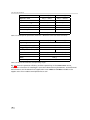
1
User Manual
MV1-D2080(IE) CameraLink® Series
BL1-D2080(IE) CameraLink® Series
CMOS Area Scan Camera
MAN047 04/2011 V1.0
All information provided in this manual is believed to be accurate and reliable. No
responsibility is assumed by Photonfocus AG for its use. Photonfocus AG reserves the right to
make changes to this information without notice.
Reproduction of this manual in whole or in part, by any means, is prohibited without prior
permission having been obtained from Photonfocus AG.
1
2
Contents
1 Preface
1.1 About Photonfocus
1.2 Contact . . . . . . .
1.3 Sales Offices . . . .
1.4 Further information
1.5 Legend . . . . . . .
.
.
.
.
.
.
.
.
.
.
.
.
.
.
.
.
.
.
.
.
.
.
.
.
.
.
.
.
.
.
.
.
.
.
.
.
.
.
.
.
.
.
.
.
.
.
.
.
.
.
.
.
.
.
.
.
.
.
.
.
.
.
.
.
.
.
.
.
.
.
.
.
.
.
.
.
.
.
.
.
.
.
.
.
.
.
.
.
.
.
.
.
.
.
.
.
.
.
.
.
.
.
.
.
.
.
.
.
.
.
.
.
.
.
.
.
.
.
.
.
.
.
.
.
.
.
.
.
.
.
.
.
.
.
.
.
.
.
.
.
.
.
.
.
.
.
.
.
.
.
.
.
.
.
.
.
.
.
.
.
.
.
.
.
.
.
.
.
.
.
.
.
.
.
.
.
.
.
.
.
.
.
.
.
.
5
5
5
5
5
6
.
.
.
.
.
2 How to get started (CameraLink® )
3 Product Specification
3.1 Introduction . . . . . . . . . . . . . . . .
3.2 Feature Overview . . . . . . . . . . . . .
3.3 Technical Specification . . . . . . . . . .
3.4 Frame Grabber relevant Configuration .
7
.
.
.
.
.
.
.
.
.
.
.
.
.
.
.
.
.
.
.
.
.
.
.
.
.
.
.
.
.
.
.
.
.
.
.
.
.
.
.
.
.
.
.
.
.
.
.
.
.
.
.
.
.
.
.
.
.
.
.
.
.
.
.
.
.
.
.
.
.
.
.
.
.
.
.
.
.
.
.
.
.
.
.
.
.
.
.
.
.
.
.
.
11
11
12
13
16
4 Functionality
4.1 Image Acquisition . . . . . . . . . . . . . . . . .
4.1.1 Readout Modes . . . . . . . . . . . . . .
4.1.2 Readout Timing . . . . . . . . . . . . . .
4.1.3 Exposure Control . . . . . . . . . . . . .
4.1.4 Maximum Frame Rate . . . . . . . . . .
4.2 Pixel Response . . . . . . . . . . . . . . . . . . .
4.2.1 Linear Response . . . . . . . . . . . . . .
4.2.2 LinLog® . . . . . . . . . . . . . . . . . . .
4.3 Reduction of Image Size . . . . . . . . . . . . .
4.3.1 Region of Interest (ROI) . . . . . . . . .
4.3.2 ROI configuration . . . . . . . . . . . . .
4.3.3 Calculation of the maximum frame rate
4.3.4 Multiple Regions of Interest . . . . . . .
4.3.5 Decimation . . . . . . . . . . . . . . . . .
4.4 Trigger and Strobe . . . . . . . . . . . . . . . .
4.4.1 Introduction . . . . . . . . . . . . . . . .
4.4.2 Trigger Source . . . . . . . . . . . . . . .
4.4.3 Exposure Time Control . . . . . . . . . .
4.4.4 Trigger Delay . . . . . . . . . . . . . . . .
4.4.5 Burst Trigger . . . . . . . . . . . . . . . .
4.4.6 Software Trigger . . . . . . . . . . . . .
4.4.7 Strobe Output . . . . . . . . . . . . . . .
4.5 Data Path Overview . . . . . . . . . . . . . . . .
4.6 Image Correction . . . . . . . . . . . . . . . . .
4.6.1 Overview . . . . . . . . . . . . . . . . . .
4.6.2 Offset Correction (FPN, Hot Pixels) . . .
.
.
.
.
.
.
.
.
.
.
.
.
.
.
.
.
.
.
.
.
.
.
.
.
.
.
.
.
.
.
.
.
.
.
.
.
.
.
.
.
.
.
.
.
.
.
.
.
.
.
.
.
.
.
.
.
.
.
.
.
.
.
.
.
.
.
.
.
.
.
.
.
.
.
.
.
.
.
.
.
.
.
.
.
.
.
.
.
.
.
.
.
.
.
.
.
.
.
.
.
.
.
.
.
.
.
.
.
.
.
.
.
.
.
.
.
.
.
.
.
.
.
.
.
.
.
.
.
.
.
.
.
.
.
.
.
.
.
.
.
.
.
.
.
.
.
.
.
.
.
.
.
.
.
.
.
.
.
.
.
.
.
.
.
.
.
.
.
.
.
.
.
.
.
.
.
.
.
.
.
.
.
.
.
.
.
.
.
.
.
.
.
.
.
.
.
.
.
.
.
.
.
.
.
.
.
.
.
.
.
.
.
.
.
.
.
.
.
.
.
.
.
.
.
.
.
.
.
.
.
.
.
.
.
.
.
.
.
.
.
.
.
.
.
.
.
.
.
.
.
.
.
.
.
.
.
.
.
.
.
.
.
.
.
.
.
.
.
.
.
.
.
.
.
.
.
.
.
.
.
.
.
.
.
.
.
.
.
.
.
.
.
.
.
.
.
.
.
.
.
.
.
.
.
.
.
.
.
.
.
.
.
.
.
.
.
.
.
.
.
.
.
.
.
.
.
.
.
.
.
.
.
.
.
.
.
.
.
.
.
.
.
.
.
.
.
.
.
.
.
.
.
.
.
.
.
.
.
.
.
.
.
.
.
.
.
.
.
.
.
.
.
.
.
.
.
.
.
.
.
.
.
.
.
.
.
.
.
.
.
.
.
.
.
.
.
.
.
.
.
.
.
.
.
.
.
.
.
.
.
.
.
.
.
.
.
.
.
.
.
.
.
.
.
.
.
.
.
.
.
.
.
.
.
.
.
.
.
.
.
.
.
.
.
.
.
.
.
.
.
.
.
.
.
.
.
.
.
.
.
.
.
.
.
.
.
.
.
.
.
.
.
.
.
.
.
.
.
.
.
.
.
.
.
.
.
.
.
.
.
.
.
.
.
.
.
.
.
.
.
.
.
.
.
.
.
.
.
.
.
.
.
.
.
.
.
.
.
.
.
.
.
.
.
.
.
.
.
.
.
.
.
.
.
.
.
.
.
.
.
.
.
.
.
.
.
.
.
.
.
.
.
.
.
.
.
.
.
.
.
.
.
.
.
.
.
.
.
.
.
.
.
19
19
19
21
24
24
25
25
25
30
30
33
33
34
37
40
40
40
40
44
44
45
45
47
48
48
48
CONTENTS
.
.
.
.
.
.
.
.
.
.
.
.
3
CONTENTS
.
.
.
.
.
.
.
.
.
.
.
.
.
.
.
.
.
.
.
.
.
.
.
.
.
.
.
.
.
.
.
.
.
.
.
.
.
.
.
.
.
.
.
.
.
.
.
.
.
.
.
.
.
.
.
.
.
.
.
.
.
.
.
.
.
.
.
.
.
.
.
.
.
.
.
.
.
.
.
.
.
.
.
.
.
.
.
.
.
.
.
.
.
.
.
.
.
.
.
.
.
.
.
.
.
.
.
.
.
.
.
.
.
.
.
.
.
.
.
.
.
.
.
.
.
.
.
.
.
.
.
.
.
.
.
.
.
.
.
.
.
.
.
.
.
.
.
.
.
.
.
.
.
.
.
.
.
.
.
.
.
.
.
.
.
.
.
.
.
.
.
.
.
.
.
.
.
.
.
.
.
.
.
.
.
.
.
.
.
.
.
.
.
.
.
.
.
.
.
.
.
.
.
.
.
.
.
.
.
.
.
.
.
.
.
.
.
.
.
.
.
.
.
.
.
.
.
.
.
.
.
.
.
.
.
.
.
.
.
.
.
.
.
.
.
.
.
.
.
.
.
.
.
.
.
.
.
.
.
.
.
.
.
.
.
.
.
.
.
.
.
.
.
.
.
.
.
.
.
.
.
.
.
.
.
.
.
.
.
.
.
.
.
.
.
.
.
.
.
.
.
.
.
.
.
.
.
.
.
.
.
.
.
.
.
.
.
.
.
.
.
.
.
.
.
.
.
.
.
.
.
.
.
.
.
.
.
.
.
.
.
.
.
.
.
.
.
.
.
.
.
.
.
.
.
.
.
.
.
.
.
.
.
.
.
.
.
.
.
.
.
.
.
.
.
.
.
.
.
.
.
.
.
.
.
.
.
.
.
.
.
.
.
.
.
.
.
.
.
.
.
.
.
.
.
.
.
.
.
.
.
.
.
.
.
.
.
.
.
.
.
.
.
.
.
.
.
.
.
.
.
.
.
.
.
.
.
.
.
.
.
.
.
.
.
.
.
.
.
.
.
.
.
.
.
.
.
.
.
.
.
.
.
.
.
.
.
.
.
.
.
.
.
.
.
.
.
.
.
.
.
.
.
.
.
.
.
.
.
.
.
.
.
.
.
.
.
.
.
.
.
.
.
.
.
.
50
51
53
53
53
55
56
56
59
59
59
59
62
62
64
64
64
66
66
66
66
69
5 Hardware Interface
5.1 Connectors . . . . . . . . . . . . . . .
5.1.1 CameraLink® Connector . . .
5.1.2 Power Supply . . . . . . . . .
5.1.3 Trigger and Strobe Signals . .
5.1.4 Status Indicator (CameraLink®
5.2 CameraLink® Data Interface . . . . .
. . . . . .
. . . . . .
. . . . . .
. . . . . .
cameras)
. . . . . .
.
.
.
.
.
.
.
.
.
.
.
.
.
.
.
.
.
.
.
.
.
.
.
.
.
.
.
.
.
.
.
.
.
.
.
.
.
.
.
.
.
.
.
.
.
.
.
.
.
.
.
.
.
.
.
.
.
.
.
.
.
.
.
.
.
.
.
.
.
.
.
.
.
.
.
.
.
.
.
.
.
.
.
.
.
.
.
.
.
.
.
.
.
.
.
.
.
.
.
.
.
.
.
.
.
.
.
.
.
.
.
.
.
.
.
.
.
.
.
.
.
.
.
.
.
.
.
.
.
.
.
.
71
71
71
71
72
73
73
6 The PFRemote Control Tool
6.1 Overview . . . . . . . . . . . . . .
6.2 PFRemote and PFLib . . . . . . .
6.3 Operating System . . . . . . . . .
6.4 Installation Notes . . . . . . . . .
6.5 Graphical User Interface (GUI) . .
6.5.1 Port Browser . . . . . . . .
6.5.2 Ports, Device Initialization
6.5.3 Main Buttons . . . . . . .
6.6 Device Properties . . . . . . . . .
.
.
.
.
.
.
.
.
.
.
.
.
.
.
.
.
.
.
.
.
.
.
.
.
.
.
.
.
.
.
.
.
.
.
.
.
.
.
.
.
.
.
.
.
.
.
.
.
.
.
.
.
.
.
.
.
.
.
.
.
.
.
.
.
.
.
.
.
.
.
.
.
.
.
.
.
.
.
.
.
.
.
.
.
.
.
.
.
.
.
.
.
.
.
.
.
.
.
.
.
.
.
.
.
.
.
.
.
.
.
.
.
.
.
.
.
.
.
.
.
.
.
.
.
.
.
.
.
.
.
.
.
.
.
.
.
.
.
.
.
.
.
.
.
.
.
.
.
.
.
.
.
.
.
.
.
.
.
.
.
.
.
.
.
.
.
.
.
.
.
.
.
.
.
.
.
.
.
.
.
.
.
.
.
.
.
.
.
.
.
.
.
.
.
.
.
.
.
.
.
.
.
.
.
.
.
.
.
.
.
.
.
.
.
.
.
.
.
.
.
.
.
.
.
.
.
.
.
.
.
.
.
.
.
.
.
.
.
.
.
.
.
.
.
.
.
.
.
.
.
.
.
.
.
.
.
.
.
.
.
.
.
.
.
.
.
.
.
.
.
75
75
75
75
75
76
76
77
78
78
7 Graphical User Interface (GUI)
7.1 MV1-D2080-160 . . . . . . .
7.1.1 Exposure . . . . . . .
7.1.2 Window . . . . . . .
7.1.3 Trigger . . . . . . . .
7.1.4 Data Output . . . . .
7.1.5 LUT (Look-Up-Table)
7.1.6 LinLog . . . . . . . . .
7.1.7 Convolver . . . . . . .
7.1.8 Correction . . . . . .
7.1.9 Info . . . . . . . . . .
.
.
.
.
.
.
.
.
.
.
.
.
.
.
.
.
.
.
.
.
.
.
.
.
.
.
.
.
.
.
.
.
.
.
.
.
.
.
.
.
.
.
.
.
.
.
.
.
.
.
.
.
.
.
.
.
.
.
.
.
.
.
.
.
.
.
.
.
.
.
.
.
.
.
.
.
.
.
.
.
.
.
.
.
.
.
.
.
.
.
.
.
.
.
.
.
.
.
.
.
.
.
.
.
.
.
.
.
.
.
.
.
.
.
.
.
.
.
.
.
.
.
.
.
.
.
.
.
.
.
.
.
.
.
.
.
.
.
.
.
.
.
.
.
.
.
.
.
.
.
.
.
.
.
.
.
.
.
.
.
.
.
.
.
.
.
.
.
.
.
.
.
.
.
.
.
.
.
.
.
.
.
.
.
.
.
.
.
.
.
.
.
.
.
.
.
.
.
.
.
.
.
.
.
.
.
.
.
.
.
.
.
.
.
.
.
.
.
.
.
.
.
.
.
.
.
.
.
.
.
.
.
.
.
.
.
.
.
.
.
.
.
.
.
.
.
.
.
.
.
.
.
.
.
.
.
.
.
.
.
.
.
.
.
.
.
.
.
.
.
.
.
.
.
.
.
.
.
.
.
.
.
.
.
.
.
.
.
.
.
.
.
.
.
.
.
.
.
.
.
79
79
80
81
83
85
87
89
90
91
93
4.7
4.8
4.9
4.10
4.11
4.12
4.13
4
4.6.3 Gain Correction . . . . . . . . . .
4.6.4 Corrected Image . . . . . . . . . .
Digital Gain and Offset . . . . . . . . . .
Grey Level Transformation (LUT) . . . .
4.8.1 Gain . . . . . . . . . . . . . . . . .
4.8.2 Gamma . . . . . . . . . . . . . . .
4.8.3 User-defined Look-up Table . . .
4.8.4 Region LUT and LUT Enable . . .
Convolver . . . . . . . . . . . . . . . . . .
4.9.1 Functionality . . . . . . . . . . . .
4.9.2 Settings . . . . . . . . . . . . . . .
4.9.3 Examples . . . . . . . . . . . . . .
Crosshairs . . . . . . . . . . . . . . . . . .
4.10.1 Functionality . . . . . . . . . . . .
Image Information and Status Line . . .
4.11.1 Counters and Average Value . .
4.11.2 Status Line . . . . . . . . . . . . .
Test Images . . . . . . . . . . . . . . . . .
4.12.1 Ramp . . . . . . . . . . . . . . . .
4.12.2 LFSR . . . . . . . . . . . . . . . . .
4.12.3 Troubleshooting using the LFSR .
Configuration Interface (CameraLink® )
.
.
.
.
.
.
.
.
.
.
.
.
.
.
.
.
.
.
.
.
.
.
.
.
.
.
.
.
.
.
.
.
.
.
.
.
.
.
.
.
.
.
.
.
.
.
.
.
.
.
.
.
.
.
.
.
.
.
.
.
.
.
.
.
.
.
.
.
.
.
.
.
.
.
.
.
.
.
.
.
.
.
.
.
.
.
.
.
.
.
.
.
.
.
.
.
8 Mechanical and Optical Considerations
8.1 Mechanical Interface . . . . . . . . . . . . . . . . .
8.1.1 MV1 cameras with CameraLink® Interface .
8.2 Optical Interface . . . . . . . . . . . . . . . . . . . .
8.2.1 Cleaning the Sensor . . . . . . . . . . . . . .
8.3 Compliance . . . . . . . . . . . . . . . . . . . . . . .
.
.
.
.
.
.
.
.
.
.
.
.
.
.
.
.
.
.
.
.
.
.
.
.
.
.
.
.
.
.
.
.
.
.
.
.
.
.
.
.
.
.
.
.
.
.
.
.
.
.
.
.
.
.
.
.
.
.
.
.
.
.
.
.
.
.
.
.
.
.
.
.
.
.
.
.
.
.
.
.
.
.
.
.
.
.
.
.
.
.
.
.
.
.
.
.
.
.
.
.
95
95
95
97
97
99
9 Warranty
101
9.1 Warranty Terms . . . . . . . . . . . . . . . . . . . . . . . . . . . . . . . . . . . . . . . . 101
9.2 Warranty Claim . . . . . . . . . . . . . . . . . . . . . . . . . . . . . . . . . . . . . . . . 101
10 References
103
A Pinouts
105
A.1 Power Supply Connector . . . . . . . . . . . . . . . . . . . . . . . . . . . . . . . . . . . 105
A.2 CameraLink® Connector . . . . . . . . . . . . . . . . . . . . . . . . . . . . . . . . . . . 106
B Revision History
CONTENTS
109
5
CONTENTS
6
1
Preface
1.1
About Photonfocus
The Swiss company Photonfocus is one of the leading specialists in the development of CMOS
image sensors and corresponding industrial cameras for machine vision, security & surveillance
and automotive markets.
Photonfocus is dedicated to making the latest generation of CMOS technology commercially
available. Active Pixel Sensor (APS) and global shutter technologies enable high speed and
high dynamic range (120 dB) applications, while avoiding disadvantages like image lag,
blooming and smear.
Photonfocus has proven that the image quality of modern CMOS sensors is now appropriate
for demanding applications. Photonfocus’ product range is complemented by custom design
solutions in the area of camera electronics and CMOS image sensors.
Photonfocus is ISO 9001 certified. All products are produced with the latest techniques in order
to ensure the highest degree of quality.
1.2
Contact
Photonfocus AG, Bahnhofplatz 10, CH-8853 Lachen SZ, Switzerland
Sales
Phone: +41 55 451 07 45
Email: [email protected]
Support
Phone: +41 55 451 01 37
Email: [email protected]
Table 1.1: Photonfocus Contact
1.3
Sales Offices
Photonfocus products are available through an extensive international distribution network
and through our key account managers. Details of the distributor nearest you and contacts to
our key account managers can be found at www.photonfocus.com.
1.4
Further information
Photonfocus reserves the right to make changes to its products and documentation without notice. Photonfocus products are neither intended nor certified for
use in life support systems or in other critical systems. The use of Photonfocus
products in such applications is prohibited.
Photonfocus is a trademark and LinLog® is a registered trademark of Photonfocus AG. CameraLink® and GigE Vision® are a registered mark of the Automated
Imaging Association. Product and company names mentioned herein are trademarks or trade names of their respective companies.
7
1 Preface
Reproduction of this manual in whole or in part, by any means, is prohibited
without prior permission having been obtained from Photonfocus AG.
Photonfocus can not be held responsible for any technical or typographical errors.
1.5
Legend
In this documentation the reader’s attention is drawn to the following icons:
Important note
Alerts and additional information
Attention, critical warning
✎
8
Notification, user guide
2
How to get started (CameraLink® )
1.
Install a suitable frame grabber in your PC.
To find a compliant frame grabber, please see the frame grabber compatibility
list at www.photonfocus.com.
2.
Install the frame grabber software.
✎
3.
Without installed frame grabber software the camera configuration tool PFRemote will not be able to communicate with the camera. Please follow the instructions of the frame grabber supplier.
Remove the camera from its packaging. Please make sure the following items are included
with your camera:
•
Power supply connector (7-pole power plug)
•
Camera body cap
If any items are missing or damaged, please contact your dealership.
4.
Remove the camera body cap from the camera and mount a suitable lens.
When removing the camera body cap or when changing the lens, the camera
should always be held with the opening facing downwards to prevent dust or
debris falling onto the CMOS sensor.
Figure 2.1: Camera with protective cap and lens.
Do not touch the sensor surface. Protect the image sensor from particles and
dirt!
9
2 How to get started (CameraLink® )
The sensor has no cover glass, therefore dust on the sensor surface may resemble
to clusters or extended regions of dead pixel.
To choose a lens, see
www.photonfocus.com.
5.
the
Lens
Finder
in
the
’Support’
area
at
Connect the camera to the frame grabber with a suitable CameraLink® cable (see Fig. 2.2).
CameraLink® cables can be purchased from Photonfocus directly (www.photonfocus.com).
Please note that Photonfocus provides appropriate solutions for your advanced vision
applications.
Figure 2.2: Camera with frame grabber, power supply and cable.
Do not connect or disconnect the CameraLink® cable while camera power is on!
For more information about CameraLink® see Section 4.13.
6.
Connect a suitable power supply to the provided 7-pole power plug. For the connector
assembly see Fig. A.1. The pinout of the connector is shown in Appendix A.
Check the correct supply voltage and polarity! Do not exceed the maximum
operating voltage of +12V DC (± 10%).
7.
Connect the power supply to the camera (see Fig. 2.2).
✎
10
The status LED on the rear of the camera will light red for a short moment, and
then flash green. For more information see Section 5.1.4.
8.
Download the camera software PFRemote to your computer.
You can find the latest version of PFRemote on the support page at
www.photonfocus.com.
9.
Install the camera software PFRemote. Please follow the instructions of the PFRemote
setup wizard.
Figure 2.3: Screen shot PFremote setup wizard
10. Start the camera software PFRemote and choose the communication port.
Figure 2.4: PFRemote start window
11. Check the status LED on the rear of the camera.
✎
The status LED lights green when an image is being produced, and it is red when
serial communication is active. For more information see Section 5.1.4.
12. You may display images using the software that is provided by the frame grabber
manufacturer.
11
2 How to get started (CameraLink® )
12
3
Product Specification
3.1
Introduction
The MV1-D2080(IE) and BL1-D2080(IE) CMOS camera series are built around the monochrome
A2080(IE) CMOS image sensor from Photonfocus, that provides a resolution of 2080 x 2080
pixels at a wide range of spectral sensitivity. It is aimed at standard applications in industrial
image processing. The MV1-D2080(IE) and BL1-D2080(IE) CMOS camera series are identical with
the exception of the camera housing. For the sake of readability the simultaneous use of MV1
and BL1 is omitted. All specification apply to both camera series.
The principal advantages are:
•
Resolution of 2080 x 2080 pixels
•
Wide spectral sensitivity from 320 nm to 1030 nm.
•
Enhanced near infrared (NIR) sensitivity with the A2080IE CMOS image sensor.
•
High quantum efficiency (> 50%).
•
High pixel fill factor (> 60%).
•
Superior signal-to-noise ratio (SNR).
•
Low power consumption at high speeds.
•
Very high resistance to blooming.
•
High dynamic range of up to 120 dB.
•
Ideal for high speed applications: Global shutter.
•
Greyscale resolution of up to 12 bit.
•
On camera shading correction.
•
3x3 Convolver for image pre-processing included on camera.
•
Up to 512 regions of interest (MROI).
•
2 look-up tables (12-to-8 bit) on user-defined image region (Region-LUT).
•
Crosshairs overlay on the image.
•
Image information and camera settings inside the image (status line).
•
Software provided for setting and storage of camera parameters.
•
The camera has a digital CameraLink® interface.
•
The compact size of 60 x 60 x 38mm3 (M42 model) makes the MV1-D2080(IE) CMOS
cameras the perfect solution for applications in which space is at a premium.
The general specification and features of the camera are listed in the following sections.
The MV1-D2080IE camera with the A2080IE sensor will be available on request.
.
13
3 Product Specification
3.2
Feature Overview
Characteristics
Interfaces
Camera Control
MV1-D2080(IE) Series
CameraLink® base configuration
PFRemote (Windows GUI) or programming library
Configuration Interface
CLSERIAL (9’600 baud up to 1.5Mbaud, user selectable)
Trigger Modes
Interface Trigger / External opto isolated trigger input
Image pre-processing
Shading Correction (Offset and Gain)
3x3 Convolver included on camera
2 look-up tables (12-to-8 bit) on user-defined image region (Region-LUT)
Features
Greyscale resolution 12 bit / 10 bit / 8 bit
Region of Interest (ROI)
Up to 512 regions of interest (MROI)
Test pattern (LFSR and grey level ramp)
Image information and camera settings inside the image (status line)
Crosshairs overlay on the image
High blooming resistance
Opto isolated trigger input and opto isolated strobe output
Table 3.1: Feature overview (see Chapter 4 for more information)
Figure 3.1: MV1-D2080(IE) CMOS camera series with M42-mount lens.
.
14
3.3
Technical Specification
Technical Parameters
Technology
Scanning system
Optical format / diagonal
MV1-D2080(IE) Series
CMOS active pixel (APS)
Progressive scan
1.3” (25.5 mm diagonal) @ maximum resolution
2/3” (11.6 mm diagonal) @ 1024 x 1024 resolution with ROI
Resolution
Pixel size
Active optical area
Random noise
2080 x 2080 pixels
8 µm x 8 µm
16.64 mm x 16.64 mm (maximum)
< 0.3 DN @ 8 bit 1)
Fixed pattern noise (FPN)
3.4 DN @ 8 bit / correction OFF 1)
Fixed pattern noise (FPN)
< 1DN @ 8 bit / correction ON 1)2)
Dark current MV1-D2080
0.65 fA / pixel @ 27 °C
Dark current MV1-D2080IE
0.79 fA / pixel @ 27 °C
Full well capacity
Spectral range MV1-D2080
~ 90 ke−
350 nm ... 980 nm (see Fig. 3.2)
Spectral range MV1-D2080IE
350 nm ... 1100 nm (see Fig. 3.3) 3)
Responsivity MV1-D2080
295 x103 DN/(J/m2 ) @ 670 nm / 8 bit
Responsivity MV1-D2080IE
305 x103 DN/(J/m2 ) @ 850 nm / 8 bit
Quantum Efficiency
> 50 %
Optical fill factor
> 60 %
Dynamic range
60 dB in linear mode, 120 dB with LinLog®
Colour format
Monochrome
Characteristic curve
Linear, LinLog®
Shutter mode
Global shutter
Greyscale resolution
12 bit / 10 bit / 8 bit
Table 3.2: General specification of the MV1-D2080(IE) camera series (Footnotes: 1) Indicated values are
typical values. 2) Indicated values are subject to confirmation. 3) If operated above 1000 nm, the image will
be unsharp.)
3.3 Technical Specification
15
3 Product Specification
MV1-D2080(IE)-160
MV1-D2080(IE)-240
10 µs ... 0.41 s
10 µs ... 0.279 s
25 ns
16.67 ns
34 fps
51fps
Pixel clock frequency
80 MHz
80MHz
Pixel clock cycle
12.5 ns
12.5 ns
2
3
Exposure Time
Exposure time increment
3)
Frame rate
( Tint = 10 µs)
Camera taps
Read out mode
sequential or simultaneous
Table 3.3: Model-specific parameters (Footnote:
3)
Maximum frame rate @ full resolution)
MV1-D2080(IE)-160
Operating temperature
0°C ... 50°C
Camera power supply
+12 V DC (± 10 %)
Trigger signal input range
Max. power consumption
MV1-D2080(IE)-240
+5 .. +15 V DC
<5W
< TBD W
Lens mount
M42x1;F-Mount–; C-Mount (1.3")
Dimensions
60 x 60 x 38 mm3
Mass
Conformity
222 g
CE / RoHS / WEE
Table 3.4: Physical characteristics and operating ranges
Fig. 3.2 shows the quantum efficiency and the responsivity of the A2080 CMOS sensor,
displayed as a function of wavelength. For more information on photometric and radiometric
measurements see the Photonfocus application notes AN006 and AN008 available in the
support area of our website www.photonfocus.com.
16
60%
QE
1200
Responsivity
50%
1000
800
30%
600
20%
Responsivity [V
V/J/m²]
Quantum
m Efficiency
40%
400
10%
200
0%
200
0
300
400
500
600
700
800
900
1000
1100
Wavelength [nm]
Figure 3.2: Spectral response of the A2080 CMOS image sensor (standard) in the MV1-2080 camera series
Fig. 3.3 shows the quantum efficiency and the responsivity of the A2080IE CMOS sensor,
displayed as a function of wavelength. The enhancement in the NIR quantum efficiency could
be used to realize applications in the 900 to 1064 nm region.
.
3.3 Technical Specification
17
3 Product Specification
60%
QE
Responsivity
1200
50%
1000
800
30%
600
20%
Responsivity [V
V/J/m²]
Quantum
m Efficiency
40%
400
10%
200
0%
0
200
300
400
500
600
700
800
900
1000
1100
Wavelength [nm]
Figure 3.3: Spectral response of the A2080IE image sensor (NIR enhanced) in the MV1-D2080IE camera
series
3.4
Frame Grabber relevant Configuration
The parameters and settings, which are essential to configure the frame grabber are shown in
the following table. The timing diagrams of the camera are given in Section 4.1.2.
MV1-D2080(IE)-160
MV1-D2080(IE)-240
80 MHz
80 MHz
2
3
12 bit / 10 bit / 8 bit
8 bit
18 clock cycles
TBD clock cycles
CC1
EXSYNC
EXSYNC
CC2
not used
not used
CC3
not used
not used
CC4
not used
not used
Pixel Clock per Tap
Number of Taps
Greyscale resolution
Line pause
Table 3.5: Summary of parameters needed for frame grabber configuration
CameraLink® port and bit assignments are compliant with the CameraLink® standard (see [CL]).
Table 3.6 shows the tap configurations for the MV1-D2080(IE)-160 cameras. For the
MV1-D2080(IE)-240 see application note AN031 for further information.
18
Bit
Tap 0
Tap 1
Tap 0
Tap 1
Tap 0
Tap 1
8 Bit
8 Bit
10 Bit
10 Bit
12 Bit
12 Bit
0 (LSB)
A0
B0
A0
C0
A0
C0
1
A1
B1
A1
C1
A1
C1
2
A2
B2
A2
C2
A2
C2
3
A3
B3
A3
C3
A3
C3
4
A4
B4
A4
C4
A4
C4
5
A5
B5
A5
C5
A5
C5
6
A6
B6
A6
C6
A6
C6
7 (MSB of 8 Bit)
A7
B7
A7
C7
A7
C7
8
-
-
B0
B4
B0
B4
9 (MSB of 10 Bit)
-
-
B1
B5
B1
B5
10
-
-
-
-
B2
B6
11 (MSB of 12 Bit)
-
-
-
-
B3
B7
Table 3.6: CameraLink® 2 Tap port and bit assignments for the MV1-D2080(IE)-160 camera
3.4 Frame Grabber relevant Configuration
19
3 Product Specification
.
20
4
Functionality
This chapter serves as an overview of the camera configuration modes and explains camera
features. The goal is to describe what can be done with the camera. The setup of the
MV1-D2080(IE) series cameras is explained in later chapters.
4.1
4.1.1
Image Acquisition
Readout Modes
The MV1-D2080(IE) CMOS cameras provide two different readout modes:
Sequential readout Frame time is the sum of exposure time and readout time. Exposure time
of the next image can only start if the readout time of the current image is finished.
Simultaneous readout (interleave) The frame time is determined by the maximum of the
exposure time or of the readout time, which ever of both is the longer one. Exposure
time of the next image can start during the readout time of the current image.
Readout Mode
MV1-D2080(IE) Series
Sequential readout
available
Simultaneous readout
available
Table 4.1: Readout mode of MV1-D2080 Series camera
The following figure illustrates the effect on the frame rate when using either the sequential
readout mode or the simultaneous readout mode (interleave exposure).
fp s = 1 /r e a d o u t tim e
F ra m e ra te
(fp s)
S im u lta n e o u s
re a d o u t m o d e
fp s = 1 /e x p o s u r e tim e
S e q u e n tia l
re a d o u t m o d e
fp s = 1 /( r e a d o u t tim e + e x p o s u r e tim e )
e x p o s u re tim e < re a d o u t tim e
e x p o s u re tim e = re a d o u t tim e
e x p o s u re tim e > re a d o u t tim e
E x p o s u re tim e
Figure 4.1: Frame rate in sequential readout mode and simultaneous readout mode
Sequential readout mode For the calculation of the frame rate only a single formula applies:
frames per second equal to the inverse of the sum of exposure time and readout time.
21
4 Functionality
Simultaneous readout mode (exposure time < readout time) The frame rate is given by the
readout time. Frames per second equal to the inverse of the readout time.
Simultaneous readout mode (exposure time > readout time) The frame rate is given by the
exposure time. Frames per second equal to the inverse of the exposure time.
The simultaneous readout mode allows higher frame rate. However, if the exposure time
greatly exceeds the readout time, then the effect on the frame rate is neglectable.
In simultaneous readout mode image output faces minor limitations. The overall
linear sensor reponse is partially restricted in the lower grey scale region.
When changing readout mode from sequential to simultaneous readout mode
or vice versa, new settings of the BlackLevelOffset and of the image correction
are required.
Sequential readout
By default the camera continuously delivers images as fast as possible ("Free-running mode")
in the sequential readout mode. Exposure time of the next image can only start if the readout
time of the current image is finished.
e x p o s u re
re a d o u t
e x p o s u re
re a d o u t
Figure 4.2: Timing in free-running sequential readout mode
When the acquisition of an image needs to be synchronised to an external event, an external
trigger can be used (refer to Section 4.4). In this mode, the camera is idle until it gets a signal
to capture an image.
e x p o s u re
re a d o u t
id le
e x p o s u re
e x te r n a l tr ig g e r
Figure 4.3: Timing in triggered sequential readout mode
Simultaneous readout (interleave exposure)
To achieve highest possible frame rates, the camera must be set to "Free-running mode" with
simultaneous readout. The camera continuously delivers images as fast as possible. Exposure
time of the next image can start during the readout time of the current image.
e x p o s u re n
re a d o u t n -1
id le
e x p o s u re n + 1
re a d o u t n
id le
re a d o u t n + 1
fr a m e tim e
Figure 4.4: Timing in free-running simultaneous readout mode (readout time> exposure time)
22
e x p o s u re n -1
id le
e x p o s u re n + 1
e x p o s u re n
re a d o u t n -1
id le
re a d o u t n
fr a m e tim e
Figure 4.5: Timing in free-running simultaneous readout mode (readout time< exposure time)
When the acquisition of an image needs to be synchronised to an external event, an external
trigger can be used (refer to Section 4.4). In this mode, the camera is idle until it gets a signal
to capture an image.
Figure 4.6: Timing in triggered simultaneous readout mode
4.1.2
Readout Timing
Sequential readout timing
By default, the camera is in free running mode and delivers images without any external
control signals. The sensor is operated in sequential readout mode, which means that the
sensor is read out after the exposure time. Then the sensor is reset, a new exposure starts and
the readout of the image information begins again. The data is output on the rising edge of
the pixel clock. The signals FRAME_VALID (FVAL) and LINE_VALID (LVAL) mask valid image
information. The signal SHUTTER indicates the active exposure period of the sensor and is shown
for clarity only.
Simultaneous readout timing
To achieve highest possible frame rates, the camera must be set to "Free-running mode" with
simultaneous readout. The camera continuously delivers images as fast as possible. Exposure
time of the next image can start during the readout time of the current image. The data is
output on the rising edge of the pixel clock. The signals FRAME_VALID (FVAL) and LINE_VALID (LVAL)
mask valid image information. The signal SHUTTER indicates the active integration phase of the
sensor and is shown for clarity only.
4.1 Image Acquisition
23
4 Functionality
P C L K
F r a m e T im e
S H U T T E R
E x p o s u re
T im e
F V A L
C P R E
L in e p a u s e
L in e p a u s e
L in e p a u s e
L V A L
F ir s t L in e
D V A L
D A T A
Figure 4.7: Timing diagram of sequential readout mode
24
L a s t L in e
P C L K
F r a m e T im e
S H U T T E R
E x p o s u re
T im e
E x p o s u re
T im e
F V A L
C P R E
L in e p a u s e
L in e p a u s e
L in e p a u s e
C P R E
L V A L
F ir s t L in e
L a s t L in e
D V A L
D A T A
Figure 4.8: Timing diagram of simultaneous readout mode (readout time > exposure time)
P C L K
F r a m e T im e
S H U T T E R
E x p o s u r e T im e
F V A L
C P R E
L in e p a u s e
L in e p a u s e
L in e p a u s e
C P R E
L V A L
F ir s t L in e
L a s t L in e
D V A L
D A T A
Figure 4.9: Timing diagram simultaneous readout mode (readout time < exposure time)
4.1 Image Acquisition
25
4 Functionality
Frame time
Frame time is the inverse of the frame rate.
Exposure time
Period during which the pixels are integrating the incoming light.
PCLK
Pixel clock on CameraLink® interface.
SHUTTER
Internal signal, shown only for clarity. Is ’high’ during the exposure
time.
FVAL (Frame Valid)
Is ’high’ while the data of one complete frame are transferred.
LVAL (Line Valid)
Is ’high’ while the data of one line are transferred. Example: To transfer
an image with 640x480 pixels, there are 480 LVAL within one FVAL active
high period. One LVAL lasts 640 pixel clock cycles.
DVAL (Data Valid)
Is ’high’ while data are valid.
DATA
Transferred pixel values. Example: For a 100x100 pixel image, there are
100 values transferred within one LVAL active high period, or 100*100
values within one FVAL period.
Line pause
Delay before the first line and after every following line when reading
out the image data.
Table 4.2: Explanation of control and data signals used in the timing diagram
These terms will be used also in the timing diagrams of Section 4.4.
4.1.3
Exposure Control
The exposure time defines the period during which the image sensor integrates the incoming
light. Refer to Table 3.3 for the allowed exposure time range.
4.1.4
Maximum Frame Rate
The maximum frame rate depends on the exposure time and the size of the image (see Section
4.3.)
.
26
4.2
4.2.1
Pixel Response
Linear Response
The camera offers a linear response between input light signal and output grey level. This can
be modified by the use of LinLog® as described in the following sections. In addition, a linear
digital gain may be applied, as follows. Please see Table 3.2 for more model-dependent
information.
Black Level Adjustment
The black level is the average image value at no light intensity. It can be adjusted by the
software by changing the black level offset. Thus, the overall image gets brighter or darker.
Use a histogram to control the settings of the black level.
4.2.2
LinLog®
Overview
The LinLog® technology from Photonfocus allows a logarithmic compression of high light
intensities inside the pixel. In contrast to the classical non-integrating logarithmic pixel, the
LinLog® pixel is an integrating pixel with global shutter and the possibility to control the
transition between linear and logarithmic mode.
In situations involving high intrascene contrast, a compression of the upper grey level region
can be achieved with the LinLog® technology. At low intensities each pixel shows a linear
response. At high intensities the response changes to logarithmic compression (see Fig. 4.10).
The transition region between linear and logarithmic response can be smoothly adjusted by
software and is continuously differentiable and monotonic.
G re y
V a lu e
S a tu r a tio n
1 0 0 %
L in e a r
R e s p o n s e
W e a k c o m p r e s s io n
R e s u ltin g L in lo g
R e s p o n s e
S tr o n g c o m p r e s s io n
0 %
V a lu e 1
V a lu e 2
L ig h t In te n s ity
Figure 4.10: Resulting LinLog2 response curve
LinLog® is controlled by up to 4 parameters (Time1, Time2, Value1 and Value2). Value1 and Value2
correspond to the LinLog® voltage that is applied to the sensor. The higher the parameters
Value1 and Value2 respectively, the stronger the compression for the high light intensities. Time1
4.2 Pixel Response
27
4 Functionality
and Time2 are normalised to the exposure time. They can be set to a maximum value of 1000,
which corresponds to the exposure time.
Examples in the following sections illustrate the LinLog® feature.
LinLog1
In the simplest way the pixels are operated with a constant LinLog® voltage which defines the
knee point of the transition.This procedure has the drawback that the linear response curve
changes directly to a logarithmic curve leading to a poor grey resolution in the logarithmic
region (see Fig. 4.12).
V
L in L o g
t
e x p
V a lu e 1
= V a lu e 2
T im e 1 = T im e 2 = m a x .
= 1 0 0 0
0
t
Figure 4.11: Constant LinLog voltage in the Linlog1 mode
Typical LinLog1 Response Curve − Varying Parameter Value1
Time1=1000, Time2=1000, Value2=Value1
300
Output grey level (8 bit) [DN]
250
V1 = 15
V1 = 16
V1 = 17
200
V1 = 18
V1 = 19
150
100
50
0
Illumination Intensity
Figure 4.12: Response curve for different LinLog settings in LinLog1 mode
.
28
LinLog2
To get more grey resolution in the LinLog® mode, the LinLog2 procedure was developed. In
LinLog2 mode a switching between two different logarithmic compressions occurs during the
exposure time (see Fig. 4.13). The exposure starts with strong compression with a high
LinLog® voltage (Value1). At Time1 the LinLog® voltage is switched to a lower voltage resulting in
a weaker compression. This procedure gives a LinLog® response curve with more grey
resolution. Fig. 4.14 and Fig. 4.15 show how the response curve is controlled by the three
parameters Value1, Value2 and the LinLog® time Time1.
Settings in LinLog2 mode, enable a fine tuning of the slope in the logarithmic
region.
V
L in L o g
t
e x p
V a lu e 1
V a lu e 2
T im e 1
0
T im e 1
T im e 2 = m a x .
= 1 0 0 0
t
Figure 4.13: Voltage switching in the Linlog2 mode
Typical LinLog2 Response Curve − Varying Parameter Time1
Time2=1000, Value1=19, Value2=14
300
T1 = 840
Output grey level (8 bit) [DN]
250
T1 = 920
T1 = 960
200
T1 = 980
T1 = 999
150
100
50
0
Illumination Intensity
Figure 4.14: Response curve for different LinLog settings in LinLog2 mode
4.2 Pixel Response
29
4 Functionality
Typical LinLog2 Response Curve − Varying Parameter Time1
Time2=1000, Value1=19, Value2=18
200
Output grey level (8 bit) [DN]
180
160
140
120
T1 = 880
T1 = 900
T1 = 920
T1 = 940
T1 = 960
T1 = 980
T1 = 1000
100
80
60
40
20
0
Illumination Intensity
Figure 4.15: Response curve for different LinLog settings in LinLog2 mode
LinLog3
To enable more flexibility the LinLog3 mode with 4 parameters was introduced. Fig. 4.16 shows
the timing diagram for the LinLog3 mode and the control parameters.
V
L in L o g
t
e x p
V a lu e 1
V a lu e 2
T im e 1
V a lu e 3 = C o n s ta n t = 0
T im e 2
T im e 1
Figure 4.16: Voltage switching in the LinLog3 mode
.
30
T im e 2
t
t
e x p
Typical LinLog2 Response Curve − Varying Parameter Time2
Time1=850, Value1=19, Value2=18
300
T2 = 950
T2 = 960
T2 = 970
T2 = 980
T2 = 990
Output grey level (8 bit) [DN]
250
200
150
100
50
0
Illumination Intensity
Figure 4.17: Response curve for different LinLog settings in LinLog3 mode
4.2 Pixel Response
31
4 Functionality
4.3
Reduction of Image Size
With Photonfocus cameras there are several possibilities to focus on the interesting parts of an
image, thus reducing the data rate and increasing the frame rate. The most commonly used
feature is Region of Interest (ROI).
4.3.1
Region of Interest (ROI)
Some applications do not need full image resolution (e.g. 2080 x 2080 pixels). By reducing the
image size to a certain region of interest (ROI), the frame rate can be drastically increased. A
region of interest can be almost any rectangular window and is specified by its position within
the full frame and its width (W) and height (H). Table 4.3 and Table 4.4 present numerical
examples of how the frame rate can be increased by reducing the ROI.
Reductions in x-direction result in a higher frame rate. Reduction in y-direction
result in a lower data bandwidth.
The minimum width of the region of interest depends on the model of the MV1D2080(IE) camera series. For more details please consult Table 4.5.
✎
It is recommended to re-adjust the settings of the shading correction each time
a new region of interest is selected.
✎
To use ROI in x direction, the DVAL feature of the framegraber must be enabled.
32
ROI Dimension [Standard]
MV1-D2080(IE)-160
2080 x 2080 (full resolution)
34
2080 x 1024
70
1024 x 2080
34
1920 x 1080 (Full HD)
67
1280 x 1024 (SXGA)
70
1280 x 768 (WXGA)
93
1280 x 720(HD ready)
99
800 x 600 (SVGA)
119
640 x 480 (VGA)
148
2080 x 900
80
2080 x 800
90
2080 x 700
102
2080 x 600
119
2080 x 512
139
2080 x 500
142
2080 x 300
232
2080 x 256
270
2080 x 200
340
2080 x 128
510
2080 x 100
634
2080 x 64
921
2080 x 32
1539
2080 x 16
2317
2080 x 3
3932
2080 x 2
4154
2080 x 1
4404
Table 4.3: Frame rates of different ROI settings (exposure time 10 µs; correction on, and sequential readout
mode).
.
4.3 Reduction of Image Size
33
4 Functionality
ROI Dimension [Standard]
MV1-D2080(IE)-240
2076 x 2080 (full resolution)
TBD
2076 x 1024
TBD
1026 x 2080
TBD
1920 x 1080 (Full HD)
TBD
1284 x 1024 (~ SXGA)
TBD
1284 x 768 (~ WXGA)
TBD
1284 x 720(~ HD ready)
TBD
804 x 600 (~ SVGA)
TBD
642 x 480 (~ VGA)
TBD
2076 x 900
TBD
2076 x 800
TBD
2076 x 700
TBD
2076 x 600
TBD
2076 x 512
TBD
2076 x 500
TBD
2080 x 300
TBD
2076 x 256
TBD
2076 x 200
TBD
2076 x 128
TBD
2076 x 100
TBD
2076 x 64
TBD
2076 x 32
TBD
2076 x 16
TBD
2076 x 3
TBD
2076 x 2
TBD
2076 x 1
TBD
Table 4.4: Frame rates of different ROI settings (exposure time 10 µs; correction on, and sequential readout
mode).
.
34
4.3.2
ROI configuration
In the MV1-D2080(IE) camera series the following two restrictions have to be respected for the
ROI configuration:
•
The width (w) of the ROI is camera model dependent and can be set almost freely. The
witdh for the camera model MV1-D2080(IE)-160 must be modulo 2, for the
MV1-D2080(IE)-240 it must be be modulo 6.
•
Setting the ROI in x direction will never increase the readout performance (fps)
•
Setting the ROI in y direction will increase the readout performance (fps)
MV1-D2080(IE)-160
MV1-D2080(IE)-240
ROI width (w)
2 ... 2080
6 ... 2076
width condition
modulo 2
modulo 6
Table 4.5: Summary of the ROI configuration restrictions for the MV1-D2080(IE) camera series indicating
the minimum ROI width (w) and the required number of pixel overlap (ovl) over the sensor middle line
The settings of the region of interest in x-direction are restricted to modulo 2 or
6 depending on the camera model.
There are no restrictions for the settings of the region of interest in y-direction.
4.3.3
Calculation of the maximum frame rate
The frame rate mainly depends on the exposure time and readout time. The frame rate is the
inverse of the frame time.
1
fps = tframe
Calculation of the frame time (sequential mode)
tframe ≥ texp + tro
Typical values of the readout time tro are given in table Table 4.6. Calculation of the frame time
(simultaneous mode)
The calculation of the frame time in simultaneous read out mode requires more detailed data
input and is skipped here for the purpose of clarity.
A frame rate calculator for calculating the maximum frame rate is available in
the support area of the Photonfocus website.
An overview of resulting frame rates in different exposure time settings is given in table Table
4.7.
4.3 Reduction of Image Size
35
4 Functionality
ROI Dimension
MV1-D2080(IE)-160
MV1-D2080(IE)-240
2080 (2076) x 2080
tro = 28.5 ms
tro = TBD ms
2080 (2076) x 1024
tro = 14.1 ms
tro = TBD ms
2080 (2076) x 512
tro = 7.2 ms
tro = TBD ms
2080 (2076) x 256
tro = 3.7 ms
tro = TBD ms
2080 (2076) x 128
tro = 1.9 ms
tro = TBD ms
2080 (2076) x 1
tro = 0.22 ms
tro = TBD ms
Table 4.6: Read out time at different ROI settings for the MV1-D2080(IE) CMOS camera series in sequential
read out mode.
Exposure time
MV1-D2080(IE)-160
MV1-D2080(IE)-240
10 µs
34 / 34 fps
TBD / TBD fps
100 µs
34 / 34 fps
TBD / TBD fps
500 µs
34 / 34 fps
TBD / TBD fps
1 ms
33 / 34 fps
TBD / TBD fps
2 ms
32 / 34 fps
TBD / TBD fps
5 ms
29 / 34 fps
TBD / TBD fps
10 ms
25 / 34 fps
TBD / TBD fps
12 ms
24 / 34 fps
TBD / TBD fps
20 ms
20 / 34 fps
TBD / TBD fps
Table 4.7: Frame rates of different exposure times, [sequential readout mode / simultaneous readout mode
], resolution 2080x 2080 pixel (MV1-D2080(IE)-240: 2076 x 2080), FPN correction on.
4.3.4
Multiple Regions of Interest
The MV1-D2080(IE) camera series can handle up to 512 different regions of interest. This
feature can be used to reduce the image data and increase the frame rate. An application
example for using multiple regions of interest (MROI) is a laser triangulation system with
several laser lines. The multiple ROIs are joined together and form a single image, which is
transferred to the frame grabber.
An individual MROI region is defined by its starting value in y-direction and its height. The
starting value in horizontal direction and the width is the same for all MROI regions and is
defined by the ROI settings. The maximum frame rate in MROI mode depends on the number
of rows and columns being read out. Overlapping ROIs are allowed. See Section 4.3.3 for
information on the calculation of the maximum frame rate.
Fig. 4.18 compares ROI and MROI: the setups (visualized on the image sensor area) are
displayed in the upper half of the drawing. The lower half shows the dimensions of the
resulting image. On the left-hand side an example of ROI is shown and on the right-hand side
an example of MROI. It can be readily seen that resulting image with MROI is smaller than the
resulting image with ROI only and the former will result in an increase in image frame rate.
Fig. 4.19 shows another MROI drawing illustrating the effect of MROI on the image content.
Fig. 4.20 shows an example from hyperspectral imaging where the presence of spectral lines at
known regions need to be inspected. By using MROI only a 656x54 region need to be readout
and a frame rate of 1053 fps can be achieved. Without using MROI the resulting frame rate
would be 34 fps for a 656x2080 ROI.
36
MROI y start values are restricted to even values.
(0 , 0 )
(0 , 0 )
M R O I 0
R O I
M R O I 1
M R O I 2
(2 0 7 9 , 2 0 7 9 )
(2 0 7 9 , 2 0 7 9 )
M R O I 0
M R O I 1
R O I
M R O I 2
Figure 4.18: Multiple Regions of Interest
.
4.3 Reduction of Image Size
37
4 Functionality
Figure 4.19: Multiple Regions of Interest with 5 ROIs
6 5 6 p ix e l
(0 , 0 )
1 p ix e l
2 p ix e l
1 p ix e l
2 0 p ix e l
2 p ix e l
2 6 p ix e l
2 p ix e l
C h e m ic a l A g e n t
A
B
Figure 4.20: Multiple Regions of Interest in hyperspectral imaging
38
C
(2 0 7 9 , 2 0 7 9 )
4.3.5
Decimation
Decimation reduces the number of pixels in y-direction. Decimation can also be used together
with ROI or MROI. Decimation in y-direction transfers every nth row only and directly results in
reduced read-out time and higher frame rate respectively.
Decimation values are limited to odd values
Fig. 4.21 shows decimation on the full image. The rows that will be read out are marked by red
lines. Row 0 is read out and then every nth row.
(0 , 0 )
(2 0 7 9 , 2 0 7 9 )
Figure 4.21: Decimation in full image
Fig. 4.22 shows decimation on a ROI. The row specified by the Window.Y setting is first read
out and then every nth row until the end of the ROI.
Fig. 4.23 shows decimation and MROI. For every MROI region m, the first row read out is the
row specified by the MROI<m>.Y setting and then every nth row until the end of MROI region
m.
The image in Fig. 4.24 on the right-hand side shows the result of decimation 3 of the image on
the left-hand side.
An example of a high-speed measurement of the elongation of an injection needle is given in
Fig. 4.25. In this application the height information is less important than the width
information. Applying decimation 3 on the original image on the left-hand side triples the
resulting frame to about TBD fps.
.
4.3 Reduction of Image Size
39
4 Functionality
(0 , 0 )
R O I
(2 0 7 9 , 2 0 7 9 )
Figure 4.22: Decimation and ROI
(0 , 0 )
R O I
M R O I 0
M R O I 1
M R O I 2
(2 0 7 9 , 2 0 7 9 )
Figure 4.23: Decimation and MROI
40
Figure 4.24: Image example of decimation 3
Figure 4.25: Example of decimation 2 on image of injection needle
4.3 Reduction of Image Size
41
4 Functionality
4.4
4.4.1
Trigger and Strobe
Introduction
The start of the exposure of the camera’s image sensor is controlled by the trigger. The trigger
can either be generated internally by the camera (free running trigger mode) or by an external
device (external trigger mode).
This section refers to the external trigger mode if not otherwise specified.
In external trigger mode, the trigger can be applied through the CameraLink ® interface
(interface trigger) or directly by the power supply connector of the camera (I/O Trigger) (see
Section 4.4.2). The trigger signal can be configured to be active high or active low. When the
frequency of the incoming triggers is higher than the maximal frame rate of the current
camera settings, then some trigger pulses will be missed. A missed trigger counter counts these
events. This counter can be read out by the user.
The exposure time in external trigger mode can be defined by the setting of the exposure time
register (camera controlled exposure mode) or by the width of the incoming trigger pulse
(trigger controlled exposure mode) (see Section 4.4.3).
An external trigger pulse starts the exposure of one image. In Burst Trigger Mode however, a
trigger pulse starts the exposure of a user defined number of images (see Section 4.4.5).
The start of the exposure is shortly after the active edge of the incoming trigger. An additional
trigger delay can be applied that delays the start of the exposure by a user defined time (see
Section 4.4.4). This often used to start the exposure after the trigger to a flash lighting source.
4.4.2
Trigger Source
The trigger signal can be configured to be active high or active low. One of the following
trigger sources can be used:
Free running The trigger is generated internally by the camera. Exposure starts immediately
after the camera is ready and the maximal possible frame rate is attained, if Constant
Frame Rate mode is disabled. In Constant Frame Rate mode, exposure starts after a
user-specified time (Frame Time) has elapsed from the previous exposure start and
therefore the frame rate is set to a user defined value.
Interface Trigger In the interface trigger mode, the trigger signal is applied to the camera by
the CameraLink® interface. Fig. 4.26 shows a diagram of the interface trigger setup. The
trigger is generated by the frame grabber board and sent on the CC1 signal through the
CameraLink® interface. Some frame grabbers allow the connection external trigger
devices through an I/O card. A schematic diagram of this setup is shown in Fig. 4.27.
I/O Trigger In the I/O trigger mode, the trigger signal is applied directly to the camera by the
power supply connector (via an optocoupler). A setup of this mode is shown in Fig. 4.28.
The electrical interface of the I/O trigger input and the strobe output is described in
Section 5.1.3.
4.4.3
Exposure Time Control
Depending on the trigger mode, the exposure time can be determined either by the camera or
by the trigger signal itself:
Camera-controlled Exposure time In this trigger mode the exposure time is defined by the
camera. For an active high trigger signal, the camera starts the exposure with a positive
trigger edge and stops it when the preprogrammed exposure time has elapsed. The
exposure time is defined by the software.
42
M a c h in e V is io n
S y s t e m P C
C a m e r a L in k
P o w e r
E X S Y N C
( C C 1 ) / S o ft t r ig g e r
F r a m e G r a b b e r
T M
A
C a m e r a
B
D a t a C a m e r a L in k
Figure 4.26: Interface trigger source
M a c h in e V is io n
S y s t e m P C
( C C 1 ) / S o ft t r ig g e r
T M
F r a m e G r a b b e r
A
E X S Y N C
C a m e r a 2
C a m e r a L in k
P o w e r
D a t a C a m e r a L in k
E X S Y N C
( C C 1 ) / S o ft t r ig g e r
B
C a m e r a 1
D a t a C a m e r a L in k
P o w e r
I / O
T r ig g e r S o u r c e
B o a r d
F la s h
Figure 4.27: Interface trigger with 2 cameras and frame grabber I/O card
Trigger-controlled Exposure time In this trigger mode the exposure time is defined by the
pulse width of the trigger pulse. For an active high trigger signal, the camera starts the
exposure with the positive edge of the trigger signal and stops it with the negative edge.
Trigger-controlled exposure time is not available in simultaneous readout mode.
External Trigger with Camera controlled Exposure Time
In the external trigger mode with camera controlled exposure time the rising edge of the
trigger pulse starts the camera states machine, which controls the sensor and optional an
4.4 Trigger and Strobe
43
4 Functionality
F la s h
M a c h in e V is io n
S y s t e m P C
T T L
C a m e r a 1
C a m e r a L in k
D a t a C a m e r a L in k
F r a m e G r a b b e r
B
T r ig g e r S o u r c e
T M
A
P o w e r
T T L
Figure 4.28: I/O trigger source
external strobe output. Fig. 4.29 shows the detailed timing diagram for the external trigger
mode with camera controlled exposure time.
e x t e r n a l t r ig g e r p u ls e in p u t
t
t r ig g e r a ft e r is o la t o r
t
d - is o - in p u t
t r ig g e r p u ls e in t e r n a l c a m e r a c o n t r o l
jit t e r
t
d e la y e d t r ig g e r fo r s h u t t e r c o n t r o l
t r ig g e r - d e la y
t
t r ig g e r - o f fs e t
t
t
e x p o s u r e
s t r o b e - d e la y
t
t
in t e r n a l s h u t t e r c o n t r o l
s tr o b e - o ffs e t
d e la y e d t r ig g e r fo r s t r o b e c o n t r o l
in t e r n a l s t r o b e c o n t r o l
s t r o b e - d u r a t io n
t
d - is o - o u t p u t
e x t e r n a l s t r o b e p u ls e o u t p u t
Figure 4.29: Timing diagram for the camera controlled exposure time
The rising edge of the trigger signal is detected in the camera control electronic which is
implemented in an FPGA. Before the trigger signal reaches the FPGA it is isolated from the
camera environment to allow robust integration of the camera into the vision system. In the
signal isolator the trigger signal is delayed by time td−iso−input . This signal is clocked into the
FPGA which leads to a jitter of tjitter . The pulse can be delayed by the time ttrigger−delay which
can be configured by a user defined value via camera software. The trigger offset delay
ttrigger−offset results then from the synchronous design of the FPGA state machines. The
exposure time texposure is controlled with an internal exposure time controller.
44
The trigger pulse from the internal camera control starts also the strobe control state machines.
The strobe can be delayed by tstrobe−delay with an internal counter which can be controlled by
the customer via software settings. The strobe offset delay tstrobe−delay results then from the
synchronous design of the FPGA state machines. A second counter determines the strobe
duration tstrobe−duration (strobe-duration). For a robust system design the strobe output is also
isolated from the camera electronic which leads to an additional delay of td−iso−output . Table
4.8 and Table 4.9 gives an overview over the minimum and maximum values of the parameters.
External Trigger with Pulsewidth controlled Exposure Time
In the external trigger mode with Pulsewidth controlled exposure time the rising edge of the
trigger pulse starts the camera states machine, which controls the sensor. The falling edge of
the trigger pulse stops the image acquisition. Additionally the optional external strobe output
is controlled by the rising edge of the trigger pulse. Timing diagram Fig. 4.30 shows the
detailed timing for the external trigger mode with pulse width controlled exposure time.
t
e x t e r n a l t r ig g e r p u ls e in p u t
e x p o s u r e
t
t r ig g e r a ft e r is o la t o r
d - is o - in p u t
t
t r ig g e r p u ls e r is in g e d g e c a m e r a c o n t r o l
jit t e r
t
d e la y e d t r ig g e r r is in g e d g e fo r s h u t t e r s e t
t r ig g e r - d e la y
t
t r ig g e r p u ls e fa llin g e d g e c a m e r a c o n t r o l
jit t e r
t
t
t r ig g e r - o f fs e t
t
t r ig g e r - d e la y
d e la y e d t r ig g e r fa llin g e d g e s h u t t e r r e s e t
in t e r n a l s h u t t e r c o n t r o l
t
e x p o s u r e
s t r o b e - d e la y
t
t
s tr o b e - o ffs e t
d e la y e d t r ig g e r fo r s t r o b e c o n t r o l
in t e r n a l s t r o b e c o n t r o l
s t r o b e - d u r a t io n
t
e x t e r n a l s t r o b e p u ls e o u t p u t
d - is o - o u t p u t
Figure 4.30: Timing diagram for the Pulsewidth controlled exposure time
The timing of the rising edge of the trigger pulse until to the start of exposure and strobe is
equal to the timing of the camera controlled exposure time (see Section 4.4.3). In this mode
however the end of the exposure is controlled by the falling edge of the trigger Pulsewidth:
The falling edge of the trigger pulse is delayed by the time td−iso−input which is results from the
signal isolator. This signal is clocked into the FPGA which leads to a jitter of tjitter . The pulse is
4.4 Trigger and Strobe
45
4 Functionality
then delayed by ttrigger−delay by the user defined value which can be configured via camera
software. After the trigger offset time ttrigger−offset the exposure is stopped.
4.4.4
Trigger Delay
The trigger delay is a programmable delay in milliseconds between the incoming trigger edge
and the start of the exposure. This feature may be required to synchronize to external strobe
with the exposure of the camera.
4.4.5
Burst Trigger
The camera includes a burst trigger engine. When enabled, it starts a predefined number of
acquisitions after one single trigger pulse. The time between two acquisitions and the number
of acquisitions can be configured by a user defined value via the camera software. The burst
trigger feature works only in the mode "Camera controlled Exposure Time".
The burst trigger signal can be configured to be active high or active low. When the frequency
of the incoming burst triggers is higher than the duration of the programmed burst sequence,
then some trigger pulses will be missed. A missed burst trigger counter counts these events.
This counter can be read out by the user.
e x t e r n a l t r ig g e r p u ls e in p u t
t
t r ig g e r a ft e r is o la t o r
t
d - is o - in p u t
t r ig g e r p u ls e in t e r n a l c a m e r a c o n t r o l
jit t e r
t
d e la y e d t r ig g e r fo r b u r s t t r ig g e r e n g in e
b u r s t - t r ig g e r - d e la y
t
t
d e la y e d t r ig g e r fo r s h u t t e r c o n t r o l
b u r s t - p e r io d - t im e
t r ig g e r - d e la y
in t e r n a l s h u t t e r c o n t r o l
t
t r ig g e r - o f fs e t
t
t
e x p o s u r e
d e la y e d t r ig g e r fo r s t r o b e c o n t r o l
s t r o b e - d e la y
t
in t e r n a l s t r o b e c o n t r o l
t
s tr o b e - o ffs e t
s t r o b e - d u r a t io n
t
e x t e r n a l s t r o b e p u ls e o u t p u t
d - is o - o u t p u t
Figure 4.31: Timing diagram for the burst trigger mode
The timing diagram of the burst trigger mode is shown in Fig. 4.31. The timing of the
"external trigger pulse input" until to the "trigger pulse internal camera control" is equal to
46
the timing in the section Fig. 4.30. This trigger pulse then starts after a user configurable burst
trigger delay time tburst−trigger−delay the internal burst engine, which generates n internal
triggers for the shutter- and the strobe-control. A user configurable value defines the time
tburst−period−time between two acquisitions.
MV1-D2080(IE)-160
MV1-D2080(IE)-160
Minimum
Maximum
45 ns
60 ns
tjitter
0
25 ns
ttrigger−delay
0
0.42 s
tburst−trigger−delay
0
0.42 s
tburst−period−time
depends on camera settings
0.42 s
ttrigger−offset (non burst mode)
100 ns
100 ns
ttrigger−offset (burst mode)
125 ns
125 ns
texposure
10 µs
0.42 s
0
0.42 s
tstrobe−offset (non burst mode)
100 ns
100 ns
tstrobe−offset (burst mode)
125 ns
125 ns
tstrobe−duration
200 ns
0.42 s
td−iso−output
45 ns
60 ns
ttrigger−pulsewidth
200 ns
n/a
1
30000
Timing Parameter
td−iso−input
tstrobe−delay
Number of bursts n
Table 4.8: Summary of timing parameters relevant in the external trigger mode using camera (MV1D2080(IE)-160)
4.4.6
Software Trigger
The software trigger enables to emulate an external trigger pulse by the camera software
through the serial data interface. It works with both burst mode enabled and disabled. As
soon as it is performed via the camera software, it will start the image acquisition(s),
depending on the usage of the burst mode and the burst configuration. The trigger mode
must be set to Interface Trigger or I/O Trigger.
4.4.7
Strobe Output
The strobe output is an opto-isolated output located on the power supply connector that can
be used to trigger a strobe. The strobe output can be used both in free-running and in trigger
mode. There is a programmable delay available to adjust the strobe pulse to your application.
The strobe output needs a separate power supply. Please see Section Section
5.1.3 and Figure Fig. 4.27 and Fig. 4.28 for more information.
.
4.4 Trigger and Strobe
47
4 Functionality
MV1-D2080(IE)-240
MV1-D2080(IE)-240
Minimum
Maximum
45 ns
60 ns
tjitter
0
16.7 ns
ttrigger−delay
0
0.28 s
tburst−trigger−delay
0
0.28 s
tburst−period−time
depends on camera settings
0.28 s
ttrigger−offset (non burst mode)
66.7 ns
66.7 ns
ttrigger−offset (burst mode)
83.3 ns
83.3 ns
10 µs
0.28 s
0
0.28 s
tstrobe−offset (non burst mode)
66.7 ns
66.7 ns
tstrobe−offset (burst mode)
83.3 ns
83.3 ns
tstrobe−duration
200 ns
0.28 s
td−iso−output
45 ns
60 ns
ttrigger−pulsewidth
200 ns
n/a
1
30000
Timing Parameter
td−iso−input
texposure
tstrobe−delay
Number of bursts n
Table 4.9: Summary of timing parameters relevant in the external trigger mode using camera (MV1D2080(IE)-240)
48
4.5
Data Path Overview
The data path is the path of the image from the output of the image sensor to the output of
the camera. The sequence of blocks is shown in figure Fig. 4.32.
I m a g e S e n s o r
F P N
C o r r e c t io n
D ig it a l O f f s e t
D ig it a l c o a r s e G a in
D ig it a l fin e G a in
L o o k - u p t a b le ( L U T )
3 x 3 C o n v o lv e r
C r o s s h a ir s in s e r t io n
S t a t u s lin e in s e r t io n
T e s t im a g e s in s e r t io n
A p p ly d a t a r e s o lu t io n
I m a g e o u tp u t
Figure 4.32: camera data path
.
4.5 Data Path Overview
49
4 Functionality
4.6
Image Correction
4.6.1
Overview
The camera possesses image pre-processing features, that compensate for non-uniformities
caused by the sensor, the lens or the illumination. This method of improving the image quality
is generally known as ’Shading Correction’ or ’Flat Field Correction’ and consists of a
combination of offset correction, gain correction and pixel interpolation.
Since the correction is performed in hardware, there is no performance limitation of the cameras for high frame rates.
The offset correction subtracts a configurable positive or negative value from the live image
and thus reduces the fixed pattern noise of the CMOS sensor. In addition, hot pixels can be
removed by interpolation. The gain correction can be used to flatten uneven illumination or to
compensate shading effects of a lens. Both offset and gain correction work on a pixel-per-pixel
basis, i.e. every pixel is corrected separately. For the correction, a black reference and a grey
reference image are required. Then, the correction values are determined automatically in the
camera.
Do not set any reference images when gain or LUT is enabled! Read the following sections very carefully.
Correction values of both reference images can be saved into the internal flash memory, but
this overwrites the factory presets. Then the reference images that are delivered by factory
cannot be restored anymore.
4.6.2
Offset Correction (FPN, Hot Pixels)
The offset correction is based on a black reference image, which is taken at no illumination
(e.g. lens aperture completely closed). The black reference image contains the fixed-pattern
noise of the sensor, which can be subtracted from the live images in order to minimise the
static noise.
Offset correction algorithm
After configuring the camera with a black reference image, the camera is ready to apply the
offset correction:
1.
Determine the average value of the black reference image.
2.
Subtract the black reference image from the average value.
3.
Mark pixels that have a grey level higher than 1008 DN (@ 12 bit) as hot pixels.
4.
Store the result in the camera as the offset correction matrix.
5.
During image acquisition, subtract the correction matrix from the acquired image and
interpolate the hot pixels (see Section 4.6.2).
50
1
4
3
1
4
4
1
2
4
2
4
3
2
3
1
4
1
1
3
4
3
1
3
4
4
a v e ra
o f b la
re fe re
p ic tu
g e
c k
n c e
re
=
1
1
1
-2
1
b la c k r e fe r e n c e
im a g e
-1
2
1
-1
1
-1
0
1
-1
2
0
-2
0
2
-2
0
0
-1
-2
-2
o ffs e t c o r r e c tio n
m a tr ix
Figure 4.33: Schematic presentation of the offset correction algorithm
How to Obtain a Black Reference Image
In order to improve the image quality, the black reference image must meet certain demands.
The detailed procedure to set the black reference image is described in Section
7.1.8.
•
The black reference image must be obtained at no illumination, e.g. with lens aperture
closed or closed lens opening.
•
It may be necessary to adjust the black level offset of the camera. In the histogram of the
black reference image, ideally there are no grey levels at value 0 DN after adjustment of
the black level offset. All pixels that are saturated black (0 DN) will not be properly
corrected (see Fig. 4.34). The peak in the histogram should be well below the hot pixel
threshold of 1008 DN @ 12 bit.
•
Camera settings may influence the grey level. Therefore, for best results the camera
settings of the black reference image must be identical with the camera settings of the
image to be corrected.
Histogram of the uncorrected black reference image
Relative number of pixels [−]
1
black level offset ok
black level offset too low
0.8
0.6
0.4
0.2
0
0
200
400
600
800
1000
Grey level, 12 Bit [DN]
1200
1400
1600
Figure 4.34: Histogram of a proper black reference image for offset correction
4.6 Image Correction
51
4 Functionality
Hot pixel correction
Every pixel that exceeds a certain threshold in the black reference image is marked as a hot
pixel. If the hot pixel correction is switched on, the camera replaces the value of a hot pixel by
an average of its neighbour pixels (see Fig. 4.35).
p
h o t
p ix e l
n -1
p
n
p
p
n
=
p
n -1
+ p
2
n + 1
n + 1
Figure 4.35: Hot pixel interpolation
4.6.3
Gain Correction
The gain correction is based on a grey reference image, which is taken at uniform illumination
to give an image with a mid grey level.
Gain correction is not a trivial feature. The quality of the grey reference image
is crucial for proper gain correction.
Gain correction algorithm
After configuring the camera with a black and grey reference image, the camera is ready to
apply the gain correction:
1.
Determine the average value of the grey reference image.
2.
Subtract the offset correction matrix from the grey reference image.
3.
Divide the average value by the offset corrected grey reference image.
4.
Pixels that have a grey level higher than a certain threshold are marked as hot pixels.
5.
Store the result in the camera as the gain correction matrix.
6.
During image acquisition, multiply the gain correction matrix from the offset-corrected
acquired image and interpolate the hot pixels (see Section 4.6.2).
Gain correction is not a trivial feature. The quality of the grey reference image
is crucial for proper gain correction.
52
a v e
o f
re fe
p ic
ra
g r
re
tu
:
g e
a y
n c e
re
1
4
3
1
4
8
4
7
9
9
6
7
7
9
2
7
3
1 0
8
9
3
1 0
4
6
1
g ra y re fe re n c e
p ic tu r e
-
1
1
1
-2
1
1
-1
2
-1
1
-1
0
1
-1
0
2
-2
0
2
-2
0
0
-1
-2
-2
o ffs e t c o r r e c tio n
m a tr ix
)
=
1
1
1
0 .9
-2
1 .2
1
1
1
0 .9
0
-1
1
1
1 .2 0 .8
1
-2
1
-2
0
0 .8
1 .3
1
-2
g a in c o r r e c tio n
m a tr ix
Figure 4.36: Schematic presentation of the gain correction algorithm
Gain correction always needs an offset correction matrix. Thus, the offset correction always has to be performed before the gain correction.
How to Obtain a Grey Reference Image
In order to improve the image quality, the grey reference image must meet certain demands.
The detailed procedure to set the grey reference image is described in Section
7.1.8.
•
The grey reference image must be obtained at uniform illumination.
Use a high quality light source that delivers uniform illumination. Standard illumination will not be appropriate.
•
When looking at the histogram of the grey reference image, ideally there are no grey
levels at full scale (4095 DN @ 12 bit). All pixels that are saturated white will not be
properly corrected (see Fig. 4.37).
•
Camera settings may influence the grey level. Therefore, the camera settings of the grey
reference image must be identical with the camera settings of the image to be corrected.
4.6.4
Corrected Image
Offset, gain and hot pixel correction can be switched on separately. The following
configurations are possible:
•
No correction
•
Offset correction only
•
Offset and hot pixel correction
•
Hot pixel correction only
•
Offset and gain correction
•
Offset, gain and hot pixel correction
4.6 Image Correction
53
4 Functionality
Histogram of the uncorrected grey reference image
Relative number of pixels [−]
1
grey reference image ok
grey reference image too bright
0.8
0.6
0.4
0.2
0
2400
2600
2800
3000
3200
3400
Grey level, 12 Bit [DN]
)
3600
3800
4000
4200
Figure 4.37: Proper grey reference image for gain correction
1
4
3
7
4
5
4
7
6
7
6
4
5
6
3
7
6
6
5
3
7
c u r r e n t im a g e
1
4
3
4
-
1
1
1
-2
1
1
-1
2
-1
1
-1
0
1
-1
2
0
-2
0
0
2
-2
0
-1
-2
-2
o ffs e t c o r r e c tio n
m a tr ix
.
1
1
1
0 .9
-2
1 .2
1
1
1
0 .9
-1
1
1
0
1 .2 0 .8
1
-2
1
-2
1
4
0
0 .8
1 .3
1
=
3
7
5
4
-2
g a in c o r r e c tio n
m a tr ix
4
7
5
7
6
4
5
6
3
5
6
4
5
6
1
3
3
4
4
c o r r e c te d im a g e
Figure 4.38: Schematic presentation of the corrected image using gain correction algorithm
In addition, the black reference image and grey reference image that are currently stored in
the camera RAM can be output.
Table 4.10 shows the minimum and maximum values of the correction matrices, i.e. the range
that the offset and gain algorithm can correct.
Offset correction
Minimum
Maximum
-1023 DN @ 12 bit
+1023 DN @ 12 bit
0.42
2.67
Gain correction
Table 4.10: Offset and gain correction ranges
.
54
4.7
Digital Gain and Offset
Gain x1, x2, x4 and x8 are digital amplifications, which means that the digital image data are
multiplied in the camera module by a factor 1, 2, 4 or 8, respectively. It is implemented as a
binary shift of the image data, which means that there will be missing codes in the output
image as the LSB’s of the gray values are set to ’0’. E.g. for gain x2, the output value is shifted
by 1 and bit 0 is set to ’0’.
A user-defined value can be subtracted from the gray value in the digital offset block. This
feature is not available in Gain x1 mode. If digital gain is applied and if the brightness of the
image is too big then the output image might be saturated. By subtracting an offset from the
input of the gain block it is possible to avoid the saturation.
4.8
Grey Level Transformation (LUT)
Grey level transformation is remapping of the grey level values of an input image to new
values. The look-up table (LUT) is used to convert the greyscale value of each pixel in an image
into another grey value. It is typically used to implement a transfer curve for contrast
expansion. The camera performs a 12-to-8-bit mapping, so that 4096 input grey levels can be
mapped to 256 output grey levels. The use of the three available modes is explained in the
next sections. Two LUT and a Region-LUT feature are available in the MV1-D2080 camera series
(see Section 4.8.4).
For MV1-D2080-240 camera series, bits 0 & 1 of the LUT input are fixed to 0.
The output grey level resolution of the look-up table (independent of gain,
gamma or user-definded mode) is always 8 bit.
There are 2 predefined functions, which generate a look-up table and transfer it
to the camera. For other transfer functions the user can define his own LUT file.
Some commonly used transfer curves are shown in Fig. 4.39. Line a denotes a negative or
inverse transformation, line b enhances the image contrast between grey values x0 and x1.
Line c shows brightness thresholding and the result is an image with only black and white grey
levels. and line d applies a gamma correction (see also Section 4.8.2).
4.8.1
Gain
The ’Gain’ mode performs a digital, linear amplification with clamping (see Fig. 4.40). It is
configurable in the range from 1.0 to 4.0 (e.g. 1.234).
4.7 Digital Gain and Offset
55
4 Functionality
y = f(x )
y
c
m a x
b
d
a
x
0
x
1
x
m a x
x
Figure 4.39: Commonly used LUT transfer curves
Grey level transformation − Gain: y = (255/1023) ⋅ a ⋅ x
y: grey level output value (8 bit) [DN]
300
250
200
150
a = 1.0
a = 2.0
a = 3.0
a = 4.0
100
50
0
0
200
400
600
800
x: grey level input value (10 bit) [DN]
Figure 4.40: Applying a linear gain with clamping to an image
56
1000
1200
4.8.2
Gamma
The ’Gamma’ mode performs an exponential amplification, configurable in the range from 0.4
to 4.0. Gamma > 1.0 results in an attenuation of the image (see Fig. 4.41), gamma < 1.0 results
in an amplification (see Fig. 4.42). Gamma correction is often used for tone mapping and
better display of results on monitor screens.
Grey level transformation − Gamma: y = (255 / 1023γ) ⋅ xγ (γ ≥ 1)
y: grey level output value (8 bit) [DN]
300
250
200
150
γ = 1.0
γ = 1.2
γ = 1.5
γ = 1.8
γ = 2.5
γ = 4.0
100
50
0
0
200
400
600
800
x: grey level input value (10 bit) [DN]
1000
1200
Figure 4.41: Applying gamma correction to an image (gamma > 1)
Grey level transformation − Gamma: y = (255 / 1023γ) ⋅ xγ (γ ≤ 1)
y: grey level output value (8 bit) [DN]
300
250
200
150
γ = 1.0
γ = 0.9
γ = 0.8
γ = 0.6
γ = 0.4
100
50
0
0
200
400
600
800
x: grey level input value (10 bit) [DN]
1000
1200
Figure 4.42: Applying gamma correction to an image (gamma < 1)
4.8 Grey Level Transformation (LUT)
57
4 Functionality
4.8.3
User-defined Look-up Table
In the ’User’ mode, the mapping of input to output grey levels can be configured arbitrarily by
the user. There is an example file in the PFRemote folder. LUT files can easily be generated
with a standard spreadsheet tool. The file has to be stored as tab delimited text file.
U s e r L U T
y = f(x )
1 2 b it
8 b it
Figure 4.43: Data path through LUT
4.8.4
Region LUT and LUT Enable
Two LUTs and a Region-LUT feature are available in the MV1-D2080(IE) camera series. Both
LUTs can be enabled independently (see 4.11). LUT 0 superseds LUT1.
When Region-LUT feature is enabled, then the LUTs are only active in a user defined region.
Examples are shown in Fig. 4.44 and Fig. 4.45.
Fig. 4.44 shows an example of overlapping Region-LUTs. LUT 0, LUT 1 and Region LUT are
enabled. LUT 0 is active in region 0 ((x00, x01), (y00, y01)) and it supersedes LUT 1 in the
overlapping region. LUT 1 is active in region 1 ((x10, x11), (y10, y11)).
Fig. 4.45 shows an example of keyhole inspection in a laser welding application. LUT 0 and LUT
1 are used to enhance the contrast by applying optimized transfer curves to the individual
regions. LUT 0 is used for keyhole inspection. LUT 1 is optimized for seam finding.
Fig. 4.46 shows the application of the Region-LUT to a camera image. The original image
without image processing is shown on the left-hand side. The result of the application of the
Region-LUT is shown on the right-hand side. One Region-LUT was applied on a small region on
the lower part of the image where the brightness has been increased.
Enable LUT 0
Enable LUT 1
Enable Region LUT
Description
-
-
-
LUT are disabled.
X
don’t care
-
LUT 0 is active on whole image.
-
X
-
LUT 1 is active on whole image.
X
-
X
LUT 0 active in Region 0.
X
X
X
LUT 0 active in Region 0 and LUT 1 active
in Region 1. LUT 0 supersedes LUT1.
Table 4.11: LUT Enable and Region LUT
.
58
y 1 0
y 0 0
(0 , 0 )
x 0 0
x 1 0
x 0 1
x 1 1
L U T 0
y 0 1
L U T 1
y 1 1
(2 0 7 9 , 2 0 7 9 )
Figure 4.44: Overlapping Region-LUT example
(0 , 0 )
(0 , 0 )
L U T 1
L U T 1
L U T 0
L U T 0
(2 0 7 9 , 2 0 7 9 )
(2 0 7 9 , 2 0 7 9 )
Figure 4.45: Region-LUT in keyhole inspection
4.8 Grey Level Transformation (LUT)
59
4 Functionality
Figure 4.46: Region-LUT example with camera image; left: original image; right: gain 4 region in the are
of the date print of the bottle
60
4.9
4.9.1
Convolver
Functionality
The "Convolver" is a discrete 2D-convolution filter with a 3x3 convolution kernel. The kernel
coefficients can be user-defined.
The M x N discrete 2D-convolution pout (x,y) of pixel pin (x,y) with convolution kernel h, scale s
and offset o is defined in Fig. 4.47.
Figure 4.47: Convolution formula
4.9.2
Settings
The following settings for the parameters are available:
Offset Offset value o (see Fig. 4.47). Range: -4096 ... 4095
Scale Scaling divisor s (see Fig. 4.47). Range: 1 ... 4095
Coefficients Coefficients of convolution kernel h (see Fig. 4.47). Range: -4096 ... 4095.
Assignment to coefficient properties is shown in Fig. 4.48.
Figure 4.48: Convolution coefficients assignment
4.9.3
Examples
Fig. 4.49 shows the result of the application of various standard convolver settings to the
original image. shows the corresponding settings for every filter.
A filter called Unsharp Mask is often used to enhance near infrared images. Fig. 4.51 shows
examples with the corresponding settings.
.
4.9 Convolver
61
4 Functionality
Figure 4.49: 3x3 Convolution filter examples 1
Figure 4.50: 3x3 Convolution filter examples 1 settings
62
Figure 4.51: Unsharp Mask Examples
4.9 Convolver
63
4 Functionality
4.10
4.10.1
Crosshairs
Functionality
The crosshairs inserts a vertical and horizontal line into the image. The width of these lines is
one pixel. The grey level is defined by a 12 bit value (0 means black, 4095 means white). This
allows to set any grey level to get the maximum contrast depending on the acquired image.
The x/y position and the grey level can be set via the camera software. Figure Fig. 4.52 shows
two examples of the activated crosshairs with different grey values. One with white lines and
the other with black lines.
Figure 4.52: Crosshairs Example with different grey values
The x- and y-positon is absolute to the sensor pixel matrix. It is independent on the ROI, MROI
or decimation configurations. Figure Fig. 4.53 shows two situations of the crosshairs
configuration. The same MROI settings is used in both situations. The crosshairs however is set
differently. The crosshairs is not seen in the image on the right, because the x- and y-position is
set outside the MROI region.
.
64
(0 , 0 )
(0 , 0 )
M R O I 0
M R O I 0
(x
M R O I 1
(x
a b s o lu t
, y
a b s o lu t
a b s o lu t
, y
a b s o lu t
, G r e y L e v e l)
M R O I 1
, G r e y L e v e l)
(2 0 7 9 , 2 0 7 9 )
(2 0 7 9 , 2 0 7 9 )
M R O I 0
M R O I 0
M R O I 1
M R O I 1
Figure 4.53: Crosshairs absolute position
4.10 Crosshairs
65
4 Functionality
4.11
Image Information and Status Line
There are camera properties available that give information about the acquired images, such
as an image counter, average image value and the number of missed trigger signals. These
properties can be queried by software. Alternatively, a status line within the image data can be
switched on that contains all the available image information.
4.11.1
Counters and Average Value
Image counter The image counter provides a sequential number of every image that is output.
After camera startup, the counter counts up from 0 (counter width 24 bit). The counter
can be reset by the camera control software.
Real Time counter The time counter starts at 0 after camera start, and counts real-time in units
of 1 micro-second. The time counter can be reset by the software in the SDK (Counter
width 32 bit).
Missed trigger counter The missed trigger counter counts trigger pulses that were ignored by
the camera because they occurred within the exposure or read-out time of an image. In
free-running mode it counts all incoming external triggers (counter width 8 bit / no wrap
around).
Missed burst trigger counter The missed burst trigger counter counts trigger pulses that were
ignored by the camera in the burst trigger mode because they occurred while the camera
still was processing the current burst trigger sequence.
Average image value The average image value gives the average of an image in 12 bit format
(0 .. 4095 DN), regardless of the currently used grey level resolution.
4.11.2
Status Line
If enabled, the status line replaces the last row of the image with camera status information.
Every parameter is coded into fields of 4 pixels (LSB first) and uses the lower 8 bits of the pixel
value, so that the total size of a parameter field is 32 bit (see Fig. 4.54). The assignment of the
parameters to the fields is listed in 4.12.
The status line is available in all camera modes.
P ix e l:
L S B
0
F F
1
M S B
2
0 0
3
A A
P r e a m b le
5 5
L S B
4
5
6
F ie ld 0
M S B
7
L S B
8
9
1 0
F ie ld 1
M S B
1 1
L S B
1 2
1 3
1 4
M S B
1 5
F ie ld 2
Figure 4.54: Status line parameters replace the last row of the image
.
66
L S B
1 6
1 7
1 8
F ie ld 3
M S B
1 9
L S B
2 0
2 1
2 2
F ie ld 4
M S B
2 3
Start pixel index
Parameter width [bit]
Parameter Description
0
32
Preamble: 0x55AA00FF
4
24
Image Counter (see Section 4.11.1)
8
32
Real Time Counter (see Section 4.11.1)
12
8
Missed Trigger Counter (see Section 4.11.1)
16
12
Image Average Value("raw" data without taking
gain settings in account) (see Section 4.11.1)
20
24
Integration Time in units of clock cycles (see Table 3.3)
24
16
Burst Trigger Number (not yet supported, fixed to 0)
28
8
Missed Burst Trigger Counter
32
11
Horizontal start position of ROI (Window.X)
36
11
Horizontal end position of ROI
(= Window.X + Window.W - 1)
40
11
Vertical start position of ROI (Window.Y)
In MROI-mode this parameter is 0
44
11
Vertical end position of ROI (Window.Y + Window.H - 1)
In MROI-mode this parameter is the total height - 1
48
2
Trigger Source
52
2
Digital Gain
56
2
Digital Offset
60
16
Camera Type Code (see 4.13)
64
32
Camera Serial Number
Table 4.12: Assignment of status line fields
Camera Model
Camera Type Code
MV1-D2080-160-CL-12 / BL1-D2080-160-CL-12
302
MV1-D2080-240-CL-8 / BL1-D2080-240-CL-8
TBD
MV1-D2080IE-160-CL-12 / BL1-D2080IE-160-CL-12
TBD
MV1-D2080IE-240-CL-8 / BL1-D2080IE-240-CL-8
TBD
Table 4.13: Type codes of MV1-D2080 and BL1-D2080 cameras series
4.11 Image Information and Status Line
67
4 Functionality
4.12
Test Images
Test images are generated in the camera FPGA, independent of the image sensor. They can be
used to check the transmission path from the camera to the frame grabber. Independent from
the configured grey level resolution, every possible grey level appears the same number of
times in a test image. Therefore, the histogram of the received image must be flat.
A test image is a useful tool to find data transmission errors that are caused most
often by a defective cable between camera and frame grabber.
The analysis of the test images with a histogram tool gives the correct result at a
resolution of TBD x TBD pixels only.
4.12.1
Ramp
Depending on the configured grey level resolution, the ramp test image outputs a constant
pattern with increasing grey level from the left to the right side (see Fig. 4.55).
Figure 4.55: Ramp test images: 8 bit output (left), 10 bit output (middle),12 (right)
4.12.2
LFSR
The LFSR (linear feedback shift register) test image outputs a constant pattern with a
pseudo-random grey level sequence containing every possible grey level that is repeated for
every row. The LFSR test pattern was chosen because it leads to a very high data toggling rate,
which stresses the interface electronic and the cable connection.
In the histogram you can see that the number of pixels of all grey values are the same.
Please refer to application note [AN026] for the calculation and the values of the LFSR test
image.
4.12.3
Troubleshooting using the LFSR
To control the quality of your complete imaging system enable the LFSR mode, set the camera
window to 1024 x 1024 pixels (x=0 and y=0) and check the histogram. If your frame grabber
application does not provide a real-time histogram, store the image and use a graphic software
tool to display the histogram.
In the LFSR (linear feedback shift register) mode the camera generates a constant
pseudo-random test pattern containing all grey levels. If the data transmission is error free, the
histogram of the received LFSR test pattern will be flat (Fig. 4.57). On the other hand, a
non-flat histogram (Fig. 4.58) indicates problems, that may be caused either by the cable, by
the connectors or by the frame grabber.
68
Figure 4.56: LFSR (linear feedback shift register) test image
A possible origin of failure message can be caused by the CameraLink® cable
which exceeds the maximum length. Also, CameraLink® cables may suffer either
from stress due to wrong installation or from severe electromagnetic interference.
.
4.12 Test Images
69
4 Functionality
Some thinner CameraLink® cables have a predefined direction. In these cables
not all twisted pairs are separately shielded to meet the RS644 standard. These
pairs are used for the transmission of the RX/TX and for the CC1 to CC4 low
frequency control signals.
Figure 4.57: LFSR test pattern received at the frame grabber and typical histogram for error-free data
transmission
Figure 4.58: LFSR test pattern received at the frame grabber and histogram containing transmission errors
CameraLink® cables contain wire pairs, which are twisted in such a way that the
cable impedance matches with the LVDS driver and receiver impedance. Excess
stress on the cable results in transmission errors which causes distorted images.
Therefore, please do not stretch and bend a CameraLink cable.
In robots applications, the stress that is applied to the CameraLink® cable is especially high due
to the fast movement of the robot arm. For such applications, special drag chain capable cables
are available. Please contact the Photonfocus Support for consulting expertise. Appropriate
CameraLink® cable solutions are available from Photonfocus.
.
70
4.13
Configuration Interface (CameraLink® )
A CameraLink® camera can be controlled by the user via a RS232 compatible asynchronous
serial interface. This interface is contained within the CameraLink® interface as shown in Fig.
4.59 and is physically not directly accessible. Instead, the serial communication is usually routed
through the frame grabber. For some frame grabbers it might be necessary to connect a serial
cable from the frame grabber to the serial interface of the PC.
C a m e ra
F ra m e g ra b b e r
P ix e l C lo c k
C C
S ig n a ls
C a m e r a L in k
C a m e r a L in k
Im a g e d a ta ,
F V A L , L V A L , D V A L
S e r ia l In te r fa c e
Figure 4.59: CameraLink serial interface for camera communication
.
4.13 Configuration Interface (CameraLink® )
71
4 Functionality
72
5
Hardware Interface
5.1
Connectors
5.1.1
CameraLink® Connector
The CameraLink® cameras are interfaced to external components via
•
a CameraLink® connector, which is defined by the CameraLink® standard as a 26 pin, 0.5"
Mini Delta-Ribbon (MDR) connector to transmit configuration, image data and trigger.
•
a subminiature connector for the power supply, 7-pin Binder series 712.
The connectors are located on the back of the camera. Fig. 5.1 shows the plugs and the status
LED which indicates camera operation.
Figure 5.1: Rear view of the CameraLink camera
The CameraLink® interface and connector are specified in [CL]. For further details including the
pinout please refer to Appendix A. This connector is used to transmit configuration, image
data and trigger signals.
5.1.2
Power Supply
The camera requires a single voltage input (see Table 3.4). The camera meets all performance
specifications using standard switching power supplies, although well-regulated linear power
supplies provide optimum performance.
It is extremely important that you apply the appropriate voltages to your camera.
Incorrect voltages will damage the camera.
For further details including the pinout please refer to Appendix A.
.
73
5 Hardware Interface
5.1.3
Trigger and Strobe Signals
The power connector contains an external trigger input and a strobe output.
The trigger input is equipped with a constant current diode which limits the
current of the optocoupler over a wide range of voltages. Trigger signals can
thus directly get connected with the input pin and there is no need for a current
limiting resistor, that depends with its value on the input voltage. The input
voltage to the TRIGGER pin must not exceed +15V DC, to avoid damage to the
internal ESD protection and the optocoupler!
In order to use the strobe output, the internal optocoupler must be powered with 5 .. 15 V DC.
The STROBE signal is an open-collector output, therefore, the user must connect a pull-up
resistor (see Table 5.1) to STROBE_VDD (5 .. 15 V DC) as shown in Fig. 5.2. This resistor should be
located directly at the signal receiver.
Figure 5.2: Circuit for the trigger input signals
The maximum sink current of the STROBE pin is 8 mA. Do not connect inductive
or capacitive loads, such loads may result in damage of the optocoupler! If the
application requires this, please use voltage suppressor diodes in parallel with
this components to protect the optocoupler.
74
STROBE_VDD
Pull-up Resistor
15 V
> 3.9 kOhm
10 V
> 2.7 kOhm
8V
> 2.2 kOhm
7V
> 1.8 kOhm
5V
> 1.0 kOhm
Table 5.1: Pull-up resistor for strobe output and different voltage levels
5.1.4
Status Indicator (CameraLink® cameras)
A dual-color LED on the back of the camera gives information about the current status of the
CameraLink® cameras.
LED Green
Green when an image is output. At slow frame rates, the LED blinks with the
FVAL signal. At high frame rates the LED changes to an apparently continuous
green light, with intensity proportional to the ratio of readout time over frame
time.
LED Red
Red indicates an active serial communication with the camera.
Table 5.2: Meaning of the LED of the CameraLink® cameras
5.2
CameraLink® Data Interface
The CameraLink® standard contains signals for transferring the image data, control
information and the serial communication.
Data signals: CameraLink® data signals contain the image data. In addition, handshaking
signals such as FVAL, LVAL and DVAL are transmitted over the same physical channel.
Camera control information: Camera control signals (CC-signals) can be defined by the camera
manufacturer to provide certain signals to the camera. There are 4 CC-signals available
and all are unidirectional with data flowing from the frame grabber to the camera. For
example, the external trigger is provided by a CC-signal (see Table 5.3 for the CC
assignment).
CC1
EXSYNC
External Trigger. May be generated either by the frame grabber itself
(software trigger) or by an external event (hardware trigger).
CC2
CTRL0
Control0. This signal is reserved for future purposes and is not used.
CC3
CTRL1
Control1. This signal is reserved for future purposes and is not used.
CC4
CTRL2
Control2. This signal is reserved for future purposes and is not used.
Table 5.3: Summary of the Camera Control (CC) signals as used by Photonfocus
Pixel clock: The pixel clock is generated on the camera and is provided to the frame grabber
for synchronisation.
5.2 CameraLink® Data Interface
75
5 Hardware Interface
Serial communication: A CameraLink® camera can be controlled by the user via a RS232
compatible asynchronous serial interface. This interface is contained within the
CameraLink® interface and is physically not directly accessible. Refer to Section 4.13 for
more information.
C a m e ra
F ra m e g ra b b e r
P ix e l C lo c k
C C
S ig n a ls
C a m e r a L in k
C a m e r a L in k
Im a g e d a ta ,
F V A L , L V A L , D V A L
S e r ia l In te r fa c e
Figure 5.3: CameraLink interface system
The frame grabber needs to be configured with the proper tap and resolution settings,
otherwise the image will be distorted or not displayed with the correct aspect ratio. Refer to
Table 3.3 and to Section 3.4 for a summary of frame grabber relevant specifications. Fig. 5.3
shows symbolically a CameraLink® system. For more information about taps refer to the
relevant application note [AN021] on the Photonfocus website.
76
6
The PFRemote Control Tool
6.1
Overview
PFRemote is a graphical configuration tool for Photonfocus cameras. The latest release can be
downloaded from the support area of www.photonfocus.com.
All Photonfocus cameras can be either configured by PFRemote, or they can be programmed
with custom software using the PFLib SDK ([PFLIB]).
6.2
PFRemote and PFLib
As shown in Fig. 6.1, the camera parameters can be controlled by PFRemote and PFLib
respectively. To grab an image use the software or the SDK that was delivered with your frame
grabber.
Figure 6.1: PFRemote and PFLib in context with the CameraLink frame grabber software
6.3
Operating System
The PFRemote GUI is available for Windows OS only. For Linux or QNX operating systems, we
provide the necessary libraries to control the camera on request, but there is no graphical user
interface available.
If you require support for Linux or QNX operating systems, you may contact us
for details of support conditions.
6.4
Installation Notes
Before installing the required software with the PFInstaller, make sure that your frame grabber
software is installed correctly.
Several DLLs are necessary in order to be able to communicate with the cameras:
77
6 The PFRemote Control Tool
•
PFCAM.DLL: The main DLL file that handles camera detection, switching to specific camera
DLL and provides the interface for the SDK.
•
’CAMERANAME’.DLL: Specific camera DLL, e.g. mv1_d1312_160.dll.
•
COMDLL.DLL: Communication DLL. This COMDLL is not necessarily CameraLink® specific, but
may depend on a CameraLink® API compatible DLL, which should also be provided by
your frame grabber manufacturer.
•
CLALLSERIAL.DLL: Interface to CameraLink® frame grabber which supports the clallserial.dll.
•
CLSER_USB.DLL: Interface to USB port.
More information about these DLLs is available in the SDK documentation [SW002].
6.5
Graphical User Interface (GUI)
PFRemote consists of a main window (Fig. 6.2) and a configuration dialog. In the main window,
the camera port can be opened or closed, and log messages are displayed at the bottom. The
configuration dialog appears as a sub window as soon as a camera port was opened
successfully. In the sub window of PFRemote the user can configure the camera properties.
The following sections describe the general structure of PFRemote.
6.5.1
Port Browser
On start, PFRemote displays a list of available communication ports in the main window.
Figure 6.2: PFRemote main window with PortBrowser and log messages
To open a camera on a specific port double click on the port name (e.g. USB). Alternatively
right click on the port name and choose Open & Configure.... The port is then queried for a
compatible Photonfocus camera.
In the PFRemote main window, there are two menus with the following entries available:
File Menu
Clear Log: Clears the log file buffer
Quit: Exit the program
Help Menu
About: Copyright notice and version information
Help F1: Invoke the online help (PFRemote documentation)
78
6.5.2
Ports, Device Initialization
After starting PFRemote, the main window as shown in Fig. 6.2 will appear. In the PortBrowser
in the upper left corner you will see a list of supported ports.
Depending on the configuration, your port names may differ, and not every port
may be functional.
If your frame grabber supports clallserial.dll version 1.1 ( CameraLink® compliant
standard Oct 2001), the name of the manufacturer is shown in the PortBrowser.
If your frame grabber supports clallserial.dll version 1.0 (CameraLink® compliant
standard Oct 2000), the PortBrowser shows either the name of the dll or the
manufacturer name or displays "Unknown".
If your frame grabber does not support clallserial.dll, copy the clserXXXX.dll of
your frame grabber in the PFRemote directory and rename it to clser.dll. The
PortBrowser will then indicate this DLL as "clser.dll at PFRemote directory".
After connecting the camera, the device can be opened with a double click on the port name
or by right-clicking on the port name and choosing Open & Configure. If the initialisation of
the camera was successful, the configuration dialog will open. The device is closed when
PFRemote is closed. Alternatively, e.g. when connecting another camera or evaluation kit, the
device can also be closed explicitely by right clicking on the port name and choosing Close.
Make sure that the configuration dialog is closed prior to closing the port.
✎
Errors, warnings or other important activities are logged in a log window at the
bottom of the main window.
If the device does not open, check the following:
•
Is the power LED of the camera active? Do you get an image in the display software of
your frame grabber?
•
Verify all cable connections and the power supply.
•
Check the communication LED of the camera: do you see some activity when you try to
access the camera?
6.5 Graphical User Interface (GUI)
79
6 The PFRemote Control Tool
6.5.3
Main Buttons
The buttons on the right side of the configuration dialog store and reset the camera
configuration.
Figure 6.3: Main buttons
Reset: Reset the camera and load the default configuration.
Store as defaults: Store the current configuration in the camera flash memory as the default
configuration. After a reset, the camera will load this configuration by default.
Settings file - File Load: Load a stored configuration from a file.
Settings file - File Save: Save current configuration to a file.
Factory Reset: Reset camera and reset the configuration to the factory defaults.
6.6
Device Properties
Cameras or sensor devices are generally addressed as ’device’ in this software. These devices
have properties that are accessed by a property name. These property names are translated
into register accesses on the driver DLL. The property names are reflected in the GUI as far as
practicable. A property name normally has a special mark up throughout this document, for
example: ExposureTime. Some properties are grouped into a structure whose member is
accessed via dot notation, e.g. Window.X (for the start X value of a region of interest). When
changing a property, the property name can always be seen in the log window of the main
program window.
80
7
Graphical User Interface (GUI)
7.1
MV1-D2080-160
This section describes the parameters of the following camera:
•
MV1-D2080-160-CL, CameraLink interface
The following sections are grouped according to the tabs in the configuration dialog.
Figure 7.1: MV1-D2080-160 frame rate and average value
Frame Rate [fps :] Shows the actual frame rate of the camera in frames per second.
Update: To update the value of the frame rate, click on this button.
Average Value: Greyscale average of the actual image. This value is in 12bit (0...4095).
Update: To update the value of the average, click on this button.
81
7 Graphical User Interface (GUI)
7.1.1
Exposure
This tab contains exposure settings.
Figure 7.2: MV1-D2080-160 exposure panel
Exposure
Exposure time [ms :] Configure the exposure time in milliseconds.
Constant Frame Rate: When the Constant Frame Rate (CFR) is switched on, the frame rate
(number of frames per second) can be varied from almost 0 up to the maximum frame
rate. Thus, fewer images can be acquired than would otherwise be possible. When
Constant Frame Rate is switched off, the camera delivers images as fast as possible,
depending on the exposure time and the read-out time.
Frame time [ms :] Configure the frame time in milliseconds. Only available if Constant Frame
Rate is enabled. The minimum frame time depends on the exposure time and readout
time.
Simultaneous readout (Interleave)
The simultaneous readout mode allows higher frame rate.
Simultaneous readout (Interleave): Enable the simultaneous readout mode.
Combination of property Trigger.Interleave and property LinLog.Mode is not
available! Combination of property Trigger.Interleave and property Trigger.LevelControlled is not available!
82
7.1.2
Window
This tab contains the settings for the region of interest.
Figure 7.3: MV1-D2080-160 window panel
Region of Interest
The region of interest (ROI) is defined as a rectangle (X, Y), (W, H) where
X: X - coordinate, starting from 0 in the upper left corner.
Y: Y - coordinate, starting from 0 in the upper left corner.
W: Window width (in steps of 2 pixel).
H: Window height.
Set to max ROI: Set Window to maximal ROI (X=0; Y=0; W=2080; H=2080).
Window width is only available in steps of 2 pixel.
When using ROI in x-direction, enable DataValid (DVAL) feature on the frame
grabber.
7.1 MV1-D2080-160
83
7 Graphical User Interface (GUI)
Decimation
Decimation reduces the number of pixels in y-direction. Decimation can also be used together
with a ROI or MROI. Decimation in y-direction transfers every n-th row only and directly results
in reduced read-out time and higher frame rate respectively.
Decimation Y: Decimation value for y-direction. Example: Value = 3 reads every third row only.
Crosshairs
Crosshairs is a cross inside the image. The crosshairs value is overlapped the original image
data. The position of the crosshairs can be configured. The unit of the grey value is always 12
bit.
Enable Crosshairs: Enable crosshairs.
X: Vertical line position of crosshairs.
Y: Horizontal line position of crosshairs
Value [12bit :] Crosshairs grey value in 12bit.
Multi - ROI
This camera can handle up to 512 different regions of interest. The multiple ROIs are joined
together and form a single image, which is transferred to the frame grabber. An ROI is defined
by its starting value in y-direction and its height. The width and the horizontal offset are
specified by X and W settings. The maximum frame rate in MROI mode depends on the
number of rows and columns being read out. Overlapping ROIs are allowed.
Enable MROI: Enable MROI. If MROI is enabled, the ROI and MROI settings cannot be changed.
Load File...: Load a user defined MROI-file into the camera. There is an exmaple file in the
PFRemote directory.
Save File...: Save the current MROI settings to a *.txt file.
H tot: Shows the sum of all MROIs as the total image height.
84
7.1.3
Trigger
This tab contains trigger and strobe settings.
Figure 7.4: MV1-D2080-160 trigger panel
Trigger
Trigger Source:
Free running: The camera continuously delivers images with a certain configurable frame rate.
Interface Trigger: The Trigger signal is applied to the camera by the CameraLink frame grabber
or the USB interface respectively.
I/O Trigger: The trigger signal is applied directly to the camera on the power supply connector.
Exposure time defined by:
Camera: The exposure time is defined by the property ExposureTime.
Trigger Pulse Width: The exposure time is defined by the pulse width of the trigger signal
(level-controlled exposure).
This property disables LinLog, Burst trigger and simultaneous readout mode.
Exposure time defined by "Trigger Pulse Width" is also known as Level controlled
trigger.
Further trigger settings:
7.1 MV1-D2080-160
85
7 Graphical User Interface (GUI)
Trigger Delay: Programmable delay in milliseconds between the incoming trigger edge and
the start of the exposure.
Trigger signal active low: Define the trigger signal to be active high (default) or active low.
Burst Trigger
An external trigger event start a predefined number of acquisition. The period time between
the acquisitions can be configured.
Enable Burst Trigger: Delay in milliseconds from the input trigger edge to the rising edge of
the strobe output signal.
Number of Burst Triggers: Set the number of burst
Burst Trigger Period [ms :] Set the time between the burst in milliseconds.
Burst Trigger Delay [ms :] Set the delay of the burst trigger in milliseconds.
Strobe
The camera generates a strobe output signal that can be used to trigger a strobe. The delay,
pulse width and polarity can be defined by software. To turn off strobe output, set
StrobePulseWidth to 0.
Strobe Delay [ms :] Delay in milliseconds from the input trigger edge to the rising edge of the
strobe output signal.
Strobe Pulse Width [ms :] The pulse width of the strobe trigger in milliseconds.
Strobe signal active low: Define the strobe output to be active high (default) or active low.
86
7.1.4
Data Output
This tab contains image data settings.
Figure 7.5: MV1-D2080-160 data output panel
Output Mode
Output Mode:
Normal: Normal mode.
LFSR: Test image. Linear feedback shift register (pseudo-random image). The pattern depends
on the grey level resolution.
Ramp: Test image. Values of pixel are incremented by 1, starting at each row. The pattern
depends on the grey level resolution.
Resolution:
8 Bit: Grey level resolution of 8 bit.
10 Bit: Grey level resolution of 10 bit.
12 Bit: Grey level resolution of 12 bit.
Digital Gain:
1x: No digital gain, normal mode.
2x: Digital gain 2.
4x: Digital gain 4.
7.1 MV1-D2080-160
87
7 Graphical User Interface (GUI)
8x: Digital gain 8.
Digital Offset: Substracts an offset from the data. Only available in gain mode. Fine gain: The
fine gain can be used to adjust the brightness of the whole image in small steps.
88
7.1.5
LUT (Look-Up-Table)
This tab contains LUT settings.
Figure 7.6: MV1-D2080-160 LUT panel
Grey level transformation is remapping of the grey level values of an input image to new
values which transform the image in some way. The look-up-table (LUT) is used to convert the
greyscale value of each pixel in an image into another grey value. It is typically used to
implement a transfer curve for contrast expansion.
This camera performs a 12-to-8-bit mapping, so that 4096 input grey levels can be mapped to
256 output grey levels (0 to 4096 and 0 to 255).
This camera support 2 LUT, both are identical. The default LUTs is a gain function with value =
1. LUT0 has higher priority as LUT1.
Both LUT can be configured with the built-in Gain / Gamma functions or with a LUT-file
LUTX
Enable LUT X Enable the LUTX
Gain: Linear function. Y = 256 / 4096 * value * X; Valid range for value [1...4].
Gamma: Gamma function. Y = 256 / 4096^value * X ^ value; Valid range for value [0.4...4].
value: Enter a value. The LUT will be calculated and downloaded to the camera.
Region LUT
Both LUT can be configured with ROI vlaues. The LUT is only working inside the the ROI values.
Overlapping is possible. LUT0 has higher priority.
Enable Region LUT: Enable the region LUT functionality.
7.1 MV1-D2080-160
89
7 Graphical User Interface (GUI)
Region of LUT:
X: X - coordinate of region LUT, starting from 0 in the upper left corner.
Y: Y - coordinate of region LUT, starting from 0 in the upper left corner.
W: Region LUT window width (in steps of 2 pixel).
H: Region LUT window height.
Set to max ROI: Set Region LUT window to maximal ROI (X=0; Y=0; W=2080; H=2080).
LUT Files
To load or save a LUT file
LUT Index: Select the LUT, you want to load or save a file.
File functions:
Load File...: Load a user defined LUT - file into the camera (*.txt tab delimited). There is an
example in the PFRemote directory (mv1_d2080_160_lut.txt).
Save File...: Save LUT from camera into a file.
90
7.1.6
LinLog
This tab contains LinLog and Skimming settings.
Figure 7.7: MV1-D2080-160 linlog panel
LinLog
The LinLog technology from Photonfocus allows a logarithmic compression of high light
intensities. In contrast to the classical non-integrating logarithmic pixel, the LinLog pixel is an
integrating pixel with global shutter and the possibility to control the transition between
linear and logarithmic mode (Section 4.2.2). There are 3 predefined LinLog settings available.
Alternatively, custom settings can be defined in the User defined Mode.
LinLog Mode: Off: LinLog is disabled. Low/Normal/High compression: Three LinLog
presettings. User defined: Value1, Time1, Value2 and Time2. The Linlog times are per
thousand of the exposure time. Time 800 means 80% of the exposure time.
7.1 MV1-D2080-160
91
7 Graphical User Interface (GUI)
7.1.7
Convolver
This tab contains the Convolver settings.
Figure 7.8: MV1-D2080-160 convolver panel
Offset
Offset: Offset value o. Range: -4096 ... 4095.
Scale
Scale: Scale value s. Range: 1 ... 4095.
Presets
Presets: Selecting a Preset modifies all Convolver values (Offset, Scale, Coefficients).
Coefficients
Coefficents: Coefficients of the convolution kernel h. Range: -4096 ... 4095.
92
7.1.8
Correction
This tab contains correction settings.
Figure 7.9: MV1-D2080-160 correction panel
Correction Mode
This camera has image pre-processing features, that compensate for non-uniformities caused
by the sensor, the lens or the illumination.
Off: No correction.
Offset: Activate offset correction
Offset + Hotpixel: Activate offset and hot pixel correction.
Hotpixel: Activate hot pixel correction.
Offset + Gain: Activate offset and gain correction.
Offset + Gain + Hotpixel: Activate offset, gain and hot pixel correction.
Black Level Offset
It may be necessary to adjust the black level offset of the camera.
Black Level Offset: Black level offset value. Use this to adjust the black level.
7.1 MV1-D2080-160
93
7 Graphical User Interface (GUI)
Calibration
Offset (FPN), Hotpixel Correction: The offset correction is based on a black reference image,
which is taken at no illumination (e.g. lens aperture completely closed). The black
reference image contains the fixed-pattern noise of the sensor, which can be subtracted
from the live images in order to minimize the static noise. Close the lens of the camera.
Click on the Validation button. If the Set Black Ref - button is still inactive, the average of
the image is out of range. Change to panel Charateristics and change the Property
BlackLevelOffset until the average of the image is between 240 and 400DN. Click again
on the Validation button and then on the Set Black Ref Button.
If only offset and hot pixel correction is needed it is not necessary to calibrate a
grey image. (see Calculate)
Gain Correction: The gain correction is based on a grey reference image, which is taken at
uniform illumination to give an image with a mid grey level.
Gain correction is not a trivial feature. The quality of the grey reference image
is crucial for proper gain correction.
Produce a grey image with an average between 2200 and 3600DN. Click on the Validation
button to check the average. If the average is in range, the Set Grey Ref button is active.
Calculate: Calculate the correction values into the camera RAM. To make the correction values
permanent, use the ’Save to Flash’ button.
Save to Flash: Save the current correction values to the internal flash memory.
This will overwrite the factory presets.
94
7.1.9
Info
This panel shows camera specific information such as type code, serial number and firmware
revision of the FPGA and microcontroller and the description of the camera interface.
Figure 7.10: MV1-D2080-160 info panel
Camera Info
Camera name: Name of the connected camera.
Typecode: Type code of the connected camera.
Serial: Serial number of the connected camera.
FPGA Sensor Revision: Firmware revision of built-in Sensor FPGA of the connected camera.
uC Revision: Firmware revision of built-in microcontroller of the connected camera.
Interface: Description of the camera interface.
Baudrate: The actual baud rate between camera and frame grabber.
For any support requests, please enclose the information provided on this tab.
7.1 MV1-D2080-160
95
7 Graphical User Interface (GUI)
Counter
The camera has the following counters.
Image: The image counter is a 24 bit real-time counter and is incremented by 1 for every new
image.
Missed Trigger: This is a counter for trigger pulses that were blocked because the trigger pulse
was received during image exposure or readout. In free-running mode it counts all pulses
received from interface trigger or from I/O trigger interface.
Missed Burst Trigger: This is a counter for burst trigger pulses that were blocked because the
burst trigger pulse was received during the last burst is not yet finished.
To update the value of the information properties, click on the Update-Button; to reset the
properties, click on the Reset-Button.
Status Line
Enable Status Line: The status line replaces the last line of an image with image information,
please refer the manual for additional information.
Temperature
Imager PCB [deg C :] The temperature of the imager PCB.
Imager [deg C :] The temperature of the imager device.
ADC PCB [deg C :] The temperature of the Analog-Digital-Converter PCB.
Update: Press this button to update all temperature values.
96
8
Mechanical and Optical Considerations
8.1
Mechanical Interface
During storage and transport, the camera should be protected against vibration, shock,
moisture and dust. The original packaging protects the camera adequately from vibration and
shock during storage and transport. Please either retain this packaging for possible later use or
dispose of it according to local regulations.
8.1.1
MV1 cameras with CameraLink® Interface
Figure 8.1: Left: M42, Middle: F-Mount, Right: C-Mount
The following figures show the mechanical drawing of the camera housing for the
MV1-D2080(IE) CMOS cameras (all values in [mm]).
M42
60
8
36.8
44
38.1
10.95
42
38.1
30
60
44
15
4
M
8
4 xM
10.95
5
8 xM
3.4
31.2
60
3.4
4
Figure 8.2: Mechanical dimensions of the CameraLink model with M42
97
8 Mechanical and Optical Considerations
F-Mount
38.3
36.8
75.1
Figure 8.3: Mechanical dimensions of the CameraLink model with F-Mount adapter
C-Mount
40.8
5
36.8
Figure 8.4: Mechanical dimensions of the CameraLink model with C-Mount adapter
98
8.2
Optical Interface
8.2.1
Cleaning the Sensor
The sensor is part of the optical path and should be handled like other optical components:
with extreme care.
Dust can obscure pixels, producing dark patches in the images captured. Dust is most visible
when the illumination is collimated. Dark patches caused by dust or dirt shift position as the
angle of illumination changes. Dust is normally not visible when the sensor is positioned at the
exit port of an integrating sphere, where the illumination is diffuse.
1.
The camera should only be cleaned in ESD-safe areas by ESD-trained personnel using wrist
straps. Ideally, the sensor should be cleaned in a clean environment. Otherwise, in dusty
environments, the sensor will immediately become dirty again after cleaning.
2.
Use a high quality, low pressure air duster (e.g. Electrolube EAD400D, pure compressed
inert gas, www.electrolube.com) to blow off loose particles. This step alone is usually
sufficient to clean the sensor of the most common contaminants.
Workshop air supply is not appropriate and may cause permanent damage to
the sensor.
3.
If further cleaning is required, use a suitable lens wiper or Q-Tip moistened with an
appropriate cleaning fluid to wipe the sensor surface as described below. Examples of
suitable lens cleaning materials are given in Table 8.1. Cleaning materials must be
ESD-safe, lint-free and free from particles that may scratch the sensor surface.
Do not use ordinary cotton buds. These do not fulfil the above requirements and
permanent damage to the sensor may result.
4.
Wipe the sensor carefully and slowly. First remove coarse particles and dirt from the
sensor using Q-Tips soaked in 2-propanol, applying as little pressure as possible. Using a
method similar to that used for cleaning optical surfaces, clean the sensor by starting at
any corner of the sensor and working towards the opposite corner. Finally, repeat the
procedure with methanol to remove streaks. It is imperative that no pressure be applied
to the surface of the sensor or to the black globe-top material (if present) surrounding the
optically active surface during the cleaning process.
8.2 Optical Interface
99
8 Mechanical and Optical Considerations
Product
Supplier
Remark
EAD400D
Airduster
Electrolube, UK
www.electrolube.com
Anticon Gold 9"x 9"
Wiper
Milliken, USA
ESD safe and suitable for
class 100 environments.
www.milliken.com
TX4025
Wiper
Texwipe
www.texwipe.com
Transplex
Swab
Texwipe
Small Q-Tips SWABS
BB-003
Q-tips
Hans J. Michael GmbH,
Germany
Large Q-Tips SWABS
CA-003
Q-tips
Hans J. Michael GmbH,
Germany
Point Slim HUBY-340
Q-tips
Hans J. Michael GmbH,
Germany
Methanol
Fluid
Johnson Matthey GmbH,
Germany
Semiconductor Grade
99.9% min (Assay),
Merck 12,6024, UN1230,
slightly flammable and
poisonous.
www.alfa-chemcat.com
2-Propanol
(Iso-Propanol)
Fluid
Johnson Matthey GmbH,
Germany
Semiconductor Grade
99.5% min (Assay) Merck
12,5227, UN1219,
slightly flammable.
www.alfa-chemcat.com
www.hjm-reinraum.de
Table 8.1: Recommended materials for sensor cleaning
For cleaning the sensor, Photonfocus recommends the products available from the suppliers as
listed in Table 8.1.
✎
.
100
Cleaning tools (except chemicals) can be purchased directly from Photonfocus
(www.photonfocus.com).
8.3
Compliance
C E
C o m p lia n c e S t a t e m e n t
W e ,
P h o t o n fo c u s A G ,
C H -8 8 5 3 L a c h e n , S w it z e r la n d
d e c la r e u n d e r o u r s o le r e s p o n s ib ility th a t th e fo llo w in g p r o d u c ts
M V -D 1 0 2 4 -2 8 -C L -1 0 , M V -D 1 0 2 4 -8 0 -C L -8 , M V -D 1 0 2 4 -1 6 0 -C L -8
M V -D 7 5 2 -2 8 -C L -1 0 , M V -D 7 5 2 -8 0 -C L -8 , M V -D 7 5 2 -1 6 0 -C L -8
M V -D 6 4 0 -3 3 -C L -1 0 , M V -D 6 4 0 -6 6 -C L -1 0 , M V -D 6 4 0 -4 8 -U 2 -8
M V -D 6 4 0 C -3 3 -C L -1 0 , M V -D 6 4 0 C -6 6 -C L -1 0 , M V -D 6 4 0 C -4 8 -U 2 -8
M V -D 1 0 2 4 E -4 0 , M V -D 7 5 2 E -4 0 , M V -D 7 5 0 E -2 0 (C a m e r a L in k a n d
U S B 2 .0 M o d e ls ), M V -D 1 0 2 4 E -8 0 , M V -D 1 0 2 4 E -1 6 0
M V -D 1 0 2 4 E -3 D 0 1 -1 6 0
M V 2 -D 1 2 8 0 -6 4 0 -C L -8
S M 2 -D 1 0 2 4 -8 0 / V is io n C a m
P S
D S 1 -D 1 0 2 4 -4 0 -C L , D S 1 -D 1 0 2 4 -4 0 -U 2 ,
D S 1 -D 1 0 2 4 -8 0 -C L , D S 1 -D 1 0 2 4 -1 6 0 -C L
D S 1
M V 1
M V 1
M V 1
-D
-D
-D
-D
1 3
1 3
1 3
2 0
1 2
1 2
1 2
8 0
-1 6
(I)(I)(IE
0 -C L
4 0 -C L , M V 1 -D 1 3 1 2 (I)-8 0 -C L , M V 1 -D 1 3 1 2 (I)-1 6 0 -C L ,
2 4 0 -C L , E L 1 -D 1 3 1 2 -1 6 0 -C L
)-1 6 0 -C L , M V 1 -D 2 0 8 0 (IE )-2 4 0 -C L
D ig ip e a te r C L B 2 6
a r e in c o m p lia n c e w ith th e b e lo w m e n tio n e d s ta n d a r d s a c c o r d in g to
th e p r o v is io n s o f E u r o p e a n S ta n d a r d s D ir e c tiv e s :
E N
E N
E N
E N
E N
E N
E N
6 1 0
6 1 0
6 1 0
6 1 0
6 1 0
6 1 0
5 5 0
0 0
0 0
0 0
0 0
0 0
0 0
2 2
- 6 - 6 - 4 - 4 - 4 - 4 : 1 9
3 : 2
2 : 2
6 : 1
4 : 1
3 : 1
2 : 1
9 4
0 0 1
0 0 1
9 9 6
9 9 6
9 9 6
9 9 5
P h o to n fo c u s A G , A p r il 2 0 1 1
Figure 8.5: CE Compliance Statement
8.3 Compliance
101
8 Mechanical and Optical Considerations
102
9
Warranty
The manufacturer alone reserves the right to recognize warranty claims.
9.1
Warranty Terms
The manufacturer warrants to distributor and end customer that for a period of two years
from the date of the shipment from manufacturer or distributor to end customer (the
"Warranty Period") that:
•
the product will substantially conform to the specifications set forth in the applicable
documentation published by the manufacturer and accompanying said product, and
•
the product shall be free from defects in materials and workmanship under normal use.
The distributor shall not make or pass on to any party any warranty or representation on
behalf of the manufacturer other than or inconsistent with the above limited warranty set.
9.2
Warranty Claim
The above warranty does not apply to any product that has been modified or altered by any party other than manufacturer, or for any defects caused by any use
of the product in a manner for which it was not designed, or by the negligence
of any party other than manufacturer.
103
9 Warranty
104
10
References
All referenced documents can be downloaded from our website at www.photonfocus.com.
CL CameraLink® Specification, January 2004
SW002 PFLib Documentation, Photonfocus, August 2005
MAN025 User Manual "microDisplayUSB2.0", Photonfocus, November 2005
AN001 Application Note "LinLog", Photonfocus, December 2002
AN006 Application Note "Quantum Efficiency", Photonfocus, February 2004
AN007 Application Note "Camera Acquisition Modes", Photonfocus, March 2004
AN008 Application Note "Photometry versus Radiometry", Photonfocus, December 2004
AN010 Application Note "Camera Clock Concepts", Photonfocus, July 2004
AN021 Application Note "CameraLink® ", Photonfocus, July 2004
AN026 Application Note "LFSR Test Images", Photonfocus, September 2005
AN030 Application Note "LinLog® Parameter Optimization Strategies", February 2009
105
10 References
106
A
Pinouts
A.1
Power Supply Connector
The power supply plugs are available from Binder connectors at www.binder-connector.de. Fig.
A.2 shows the power supply plug from the solder side. The pin assignment of the power supply
plug is given in Table A.2.
It is extremely important that you apply the appropriate voltages to your camera.
Incorrect voltages will damage or destroy the camera.
Figure A.1: Power connector assembly
Connector Type
Order Nr.
7-pole, plastic
99-0421-00-07
7-pole, metal
99-0421-10-07
Table A.1: Power supply connectors (Binder subminiature series 712)
107
A Pinouts
7
6
1
5
2
3
4
Figure A.2: Power supply plug, 7-pole (rear view of plug, solder side)
Pin
I/O Type
Name
Description
1
PWR
VDD
+12 V DC (± 10%)
2
PWR
GND
Ground
3
O
RESERVED
Do not connect
4
PWR
STROBE-VDD
+5 .. +15 V DC
5
O
STROBE
Strobe control (opto-isolated)
6
I
TRIGGER
External trigger (opto-isolated), +5 .. +15V DC
7
PWR
GROUND
Signal ground (for opto-isolated strobe signal)
Table A.2: Power supply plug pin assignment
A.2
CameraLink® Connector
The pinout for the CameraLink® 26 pin, 0.5" Mini D-Ribbon (MDR) connector is according to
the CameraLink® standard ([CL]) and is listed here for reference only (see Table A.3). The
drawing of the CameraLink® cable plug is shown in Fig. A.3.
CameraLink® cables can
(www.photonfocus.com).
be
purchased
1
2
3
4
5
6
7
8
9
1 4
1 5
1 6
1 7
1 8
1 9
2 0
2 1
2 2
Figure A.3: CameraLink cable 3M MDR-26 plug (both ends)
.
108
1 0
2 3
1 1
2 4
from
1 2
2 5
1 3
2 6
Photonfocus
directly
PIN
IO
Name
Description
1
PW
SHIELD
Shield
2
O
N_XD0
Negative LVDS Output, CameraLink® Data D0
3
O
N_XD1
Negative LVDS Output, CameraLink® Data D1
4
O
N_XD2
Negative LVDS Output, CameraLink® Data D2
5
O
N_XCLK
Negative LVDS Output, CameraLink® Clock
6
O
N_XD3
Negative LVDS Output, CameraLink® Data D3
7
I
P_SERTOCAM
Positive LVDS Input, Serial Communication to the camera
8
O
N_SERTOFG
Negative LVDS Output, Serial Communication from the camera
9
I
N_CC1
Negative LVDS Input, Camera Control 1 (CC1)
10
I
N_CC2
Positive LVDS Input, Camera Control 2 (CC2)
11
I
N_CC3
Negative LVDS Input, Camera Control 3 (CC3)
12
I
P_CC4
Positive LVDS Input, Camera Control 4 (CC4)
13
PW
SHIELD
Shield
14
PW
SHIELD
Shield
15
O
P_XD0
Positive LVDS Output, CameraLink® Data D0
16
O
P_XD1
Positive LVDS Output, CameraLink® Data D1
17
O
P_XD2
Positive LVDS Output, CameraLink® Data D2
18
O
P_XCLK
Positive LVDS Output, CameraLink® Clock
19
O
P_XD3
Positive LVDS Output, CameraLink® Data D3
20
I
N_SERTOCAM
Negative LVDS Input, Serial Communication to the camera
21
O
P_SERTOFG
Positive LVDS Output, Serial Communication from the camera
22
I
P_CC1
Positive LVDS Input, Camera Control 1 (CC1)
23
I
N_CC2
Negative LVDS Input, Camera Control 2 (CC2)
24
I
P_CC3
Positive LVDS Input, Camera Control 3 (CC3)
25
I
N_CC4
Negative LVDS Input, Camera Control 4 (CC4)
26
PW
SHIELD
Shield
S
PW
SHIELD
Shield
Table A.3: Pinout of the CameraLink® connector
.
A.2 CameraLink® Connector
109
A Pinouts
110
B
Revision History
Revision
Date
Changes
1.0
April 2011
First release
111