1
UM1619
User manual
General purpose ST7540 power line modem module based on
ST7540 PLM and STM32 microcontroller
Introduction
This document explains how to use and setup the firmware and the software designed for
the STEVAL-IHP005V1 board and all the necessary setup for using the hardware.
The application firmware uses the ST7540 power line modem firmware stack driver
described in the UM1573: “ST7540 power line modem firmware stack”, and is organized in a
layer structure. A dedicated layer allows the user to design his own application interfacing to
the module features with very simple and easy to use APIs. A dedicated software graphical
user interface (GUI) allows the user to use all the embedded features interfacing the PLM
module with the PC via an RS232 communication port.
This firmware is developed using STM32F10x Standard Peripherals Library Rel.3.5.0 and
IAR Embedded Workbench® IDE for STM32 microcontrollers Rel. 6.3
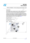
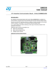
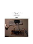
The STEVAL-IHP005V1 hardware module embeds an ARM 32-bit Cortex™-M3 core-based
STM32F103xB and a FSK power line transceiver ST7540.
Figure 1. STEVAL-IHP005V1
May 2013
DocID024383 Rev 1
1/56
www.st.com
Contents
UM1619
Contents
1
Features . . . . . . . . . . . . . . . . . . . . . . . . . . . . . . . . . . . . . . . . . . . . . . . . . . . 4
2
Hardware description . . . . . . . . . . . . . . . . . . . . . . . . . . . . . . . . . . . . . . . . 5
3
Getting started . . . . . . . . . . . . . . . . . . . . . . . . . . . . . . . . . . . . . . . . . . . . . . 8
3.1
System requirements . . . . . . . . . . . . . . . . . . . . . . . . . . . . . . . . . . . . . . . . . 8
3.2
Software installation . . . . . . . . . . . . . . . . . . . . . . . . . . . . . . . . . . . . . . . . . . 8
4
Hardware installation . . . . . . . . . . . . . . . . . . . . . . . . . . . . . . . . . . . . . . . 11
5
Software GUI description . . . . . . . . . . . . . . . . . . . . . . . . . . . . . . . . . . . . 13
6
2/56
5.1
Introduction . . . . . . . . . . . . . . . . . . . . . . . . . . . . . . . . . . . . . . . . . . . . . . . 13
5.2
Configuration tab . . . . . . . . . . . . . . . . . . . . . . . . . . . . . . . . . . . . . . . . . . . 13
5.3
Dongle tab . . . . . . . . . . . . . . . . . . . . . . . . . . . . . . . . . . . . . . . . . . . . . . . . 16
5.4
Operations tab . . . . . . . . . . . . . . . . . . . . . . . . . . . . . . . . . . . . . . . . . . . . . 17
5.5
Program tab . . . . . . . . . . . . . . . . . . . . . . . . . . . . . . . . . . . . . . . . . . . . . . . 19
5.6
Service tab . . . . . . . . . . . . . . . . . . . . . . . . . . . . . . . . . . . . . . . . . . . . . . . . 20
5.7
Sniffer tab . . . . . . . . . . . . . . . . . . . . . . . . . . . . . . . . . . . . . . . . . . . . . . . . . 22
Firmware description . . . . . . . . . . . . . . . . . . . . . . . . . . . . . . . . . . . . . . . 25
6.1
Introduction . . . . . . . . . . . . . . . . . . . . . . . . . . . . . . . . . . . . . . . . . . . . . . . 25
6.2
Remote firmware update (RFU) . . . . . . . . . . . . . . . . . . . . . . . . . . . . . . . . 25
6.3
Firmware download . . . . . . . . . . . . . . . . . . . . . . . . . . . . . . . . . . . . . . . . . 28
6.4
Firmware description . . . . . . . . . . . . . . . . . . . . . . . . . . . . . . . . . . . . . . . . 29
6.5
Firmware data types . . . . . . . . . . . . . . . . . . . . . . . . . . . . . . . . . . . . . . . . . 31
6.6
Firmware frame types . . . . . . . . . . . . . . . . . . . . . . . . . . . . . . . . . . . . . . . . 34
6.6.1
Data Frames . . . . . . . . . . . . . . . . . . . . . . . . . . . . . . . . . . . . . . . . . . . . . 34
6.6.2
Ping Frames . . . . . . . . . . . . . . . . . . . . . . . . . . . . . . . . . . . . . . . . . . . . . 35
6.6.3
Error Frames . . . . . . . . . . . . . . . . . . . . . . . . . . . . . . . . . . . . . . . . . . . . . 35
6.6.4
Acknowledgment Frames . . . . . . . . . . . . . . . . . . . . . . . . . . . . . . . . . . . 36
6.6.5
Programming Frames . . . . . . . . . . . . . . . . . . . . . . . . . . . . . . . . . . . . . . 36
6.6.6
Programming Frames . . . . . . . . . . . . . . . . . . . . . . . . . . . . . . . . . . . . . . 40
6.6.7
Embedded module features APIs . . . . . . . . . . . . . . . . . . . . . . . . . . . . . 46
DocID024383 Rev 1
UM1619
Contents
Appendix A Schematic diagrams and bill of material . . . . . . . . . . . . . . . . . . . . . 47
A.1
Bill of material . . . . . . . . . . . . . . . . . . . . . . . . . . . . . . . . . . . . . . . . . . . . . . 49
Appendix B CRC 16 calculation . . . . . . . . . . . . . . . . . . . . . . . . . . . . . . . . . . . . . . 53
References . . . . . . . . . . . . . . . . . . . . . . . . . . . . . . . . . . . . . . . . . . . . . . . . . . . . . . . . . 54
7
Revision history . . . . . . . . . . . . . . . . . . . . . . . . . . . . . . . . . . . . . . . . . . . 55
DocID024383 Rev 1
3/56
List of figures
UM1619
List of figures
Figure 1.
Figure 2.
Figure 3.
Figure 4.
Figure 5.
Figure 6.
Figure 7.
Figure 8.
Figure 9.
Figure 10.
Figure 11.
Figure 12.
Figure 13.
Figure 14.
Figure 15.
Figure 16.
Figure 17.
Figure 18.
Figure 19.
Figure 20.
Figure 21.
Figure 22.
Figure 23.
Figure 24.
Figure 25.
Figure 26.
Figure 27.
4/56
STEVAL-IHP005V1 . . . . . . . . . . . . . . . . . . . . . . . . . . . . . . . . . . . . . . . . . . . . . . . . . . . . . . . 1
STEVAL-IHP005V1 block diagram . . . . . . . . . . . . . . . . . . . . . . . . . . . . . . . . . . . . . . . . . . . . 5
Three phase connection . . . . . . . . . . . . . . . . . . . . . . . . . . . . . . . . . . . . . . . . . . . . . . . . . . . . 6
User interface connector . . . . . . . . . . . . . . . . . . . . . . . . . . . . . . . . . . . . . . . . . . . . . . . . . . . 7
Programming connector JTAG adapter . . . . . . . . . . . . . . . . . . . . . . . . . . . . . . . . . . . . . . . . 7
Installation window . . . . . . . . . . . . . . . . . . . . . . . . . . . . . . . . . . . . . . . . . . . . . . . . . . . . . . . . 8
License window . . . . . . . . . . . . . . . . . . . . . . . . . . . . . . . . . . . . . . . . . . . . . . . . . . . . . . . . . . 9
Destination folder window . . . . . . . . . . . . . . . . . . . . . . . . . . . . . . . . . . . . . . . . . . . . . . . . . . . 9
Installation status window . . . . . . . . . . . . . . . . . . . . . . . . . . . . . . . . . . . . . . . . . . . . . . . . . . 10
RS232 connection . . . . . . . . . . . . . . . . . . . . . . . . . . . . . . . . . . . . . . . . . . . . . . . . . . . . . . . 11
GUI options tab . . . . . . . . . . . . . . . . . . . . . . . . . . . . . . . . . . . . . . . . . . . . . . . . . . . . . . . . . . 12
GUI configuration tab . . . . . . . . . . . . . . . . . . . . . . . . . . . . . . . . . . . . . . . . . . . . . . . . . . . . . 14
GUI dongle tab . . . . . . . . . . . . . . . . . . . . . . . . . . . . . . . . . . . . . . . . . . . . . . . . . . . . . . . . . . 17
GUI operations tab . . . . . . . . . . . . . . . . . . . . . . . . . . . . . . . . . . . . . . . . . . . . . . . . . . . . . . . 18
GUI program tab . . . . . . . . . . . . . . . . . . . . . . . . . . . . . . . . . . . . . . . . . . . . . . . . . . . . . . . . . 19
GUI service tab . . . . . . . . . . . . . . . . . . . . . . . . . . . . . . . . . . . . . . . . . . . . . . . . . . . . . . . . . . 20
PLM communication parameters window . . . . . . . . . . . . . . . . . . . . . . . . . . . . . . . . . . . . . . 21
GUI sniffer tab. . . . . . . . . . . . . . . . . . . . . . . . . . . . . . . . . . . . . . . . . . . . . . . . . . . . . . . . . . . 22
Sniffer information. . . . . . . . . . . . . . . . . . . . . . . . . . . . . . . . . . . . . . . . . . . . . . . . . . . . . . . . 23
Module firmware structure . . . . . . . . . . . . . . . . . . . . . . . . . . . . . . . . . . . . . . . . . . . . . . . . . 25
Memory organization . . . . . . . . . . . . . . . . . . . . . . . . . . . . . . . . . . . . . . . . . . . . . . . . . . . . . 26
RFU flow chart . . . . . . . . . . . . . . . . . . . . . . . . . . . . . . . . . . . . . . . . . . . . . . . . . . . . . . . . . . 27
Active project selection . . . . . . . . . . . . . . . . . . . . . . . . . . . . . . . . . . . . . . . . . . . . . . . . . . . . 28
Workspace structure . . . . . . . . . . . . . . . . . . . . . . . . . . . . . . . . . . . . . . . . . . . . . . . . . . . . . . 29
Schematic diagrams (1 of 3) . . . . . . . . . . . . . . . . . . . . . . . . . . . . . . . . . . . . . . . . . . . . . . . . 47
Schematic diagrams (2 of 3) . . . . . . . . . . . . . . . . . . . . . . . . . . . . . . . . . . . . . . . . . . . . . . . . 48
Schematic diagrams (3 of 3) . . . . . . . . . . . . . . . . . . . . . . . . . . . . . . . . . . . . . . . . . . . . . . . . 49
DocID024383 Rev 1
UM1619
1
Features
Features
• Configurable FSK power line modem interface with an embedded firmware stack for a
complete power line communication management
• 8 user configurable general purpose input/output pins
• USART and SPI communication channel for module interfacing
• Internal configurable RTC module with lithium backup battery
• Programmable user data and PLM parameters Flash memory area
• Remote firmware update
• Embedded AES 128 encryption module with programmable AES Key
DocID024383 Rev 1
5/56
Hardware description
2
UM1619
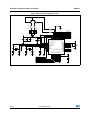
Hardware description
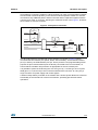
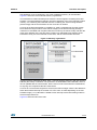
The STEVAL-IHP005V1 block diagram is shown in Figure 2. The general purpose power
line modem module is based on an ST7540 FSK power line modem transceiver and an
ARM 32-bit Cortex™-M3 core-based STM32F103xB microcontroller. The PLM module
board is a fully functional communication module, with 8 programmable I/Os, a real-time
clock and a Flash memory area for modem parameters and user data storage. The firmware
structure is made up of several layers, each dealing with a different feature. The application
layer engine is the general interface between the user program and all the parts of the
module. It manages the communication ports, the module peripherals such as SPI, SCI,
RTC, I/Os, LEDs and timing management. It is also the interface between the PLM stack
and the user program. The PLM stack, itself made up of several layers, implements and
manages the power line communication, manages the conflicts, timing and repetitions, the
addressing, and so on. Please refer to UM1573 for details on the firmware stack driver.
Some features are managed directly by the application engine, and are transparent to the
user, such as the RTC management or the module parameter update, as well as the module
programming and configuration, which is done by particular programming or service
commands managed and acknowledged directly by the application engine. Even the remote
firmware update is managed by the application engine and allows the firmware module
being update remotely by power line module.
The user layer is fully customizable by using some easy-to-use APIs available for user
application implementation. User data can be easily addressed to the PLM or to the other
communication interface by simply changing the destination channel in the user data
structure.
The STEVAL-IHP005V1 is powered by a dual regulated DC power source, +12 VDC (pin 1)
and +3.3 VDC (pin 2) from the power supply connector (J2). Pin 3 is the ground.
The communication is done via power line, which is applied to the board using the J1
connector, where pin 1 must be connected to the neutral wire and pin 3 to the phase wire
(refer to Appendix A).
Figure 2. STEVAL-IHP005V1 block diagram
WKtZ>/E
DKh>/EdZ&
^dDϯϮ
W>D
<hWddZz
6/56
DocID024383 Rev 1
Z^ϮϯϮ
UM1619
Hardware description
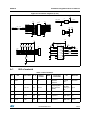
It is possible to connect the module in a three phase line (in case of communication modules
are connected in all three phases), in this case an external capacitor of 68nF X1 must be
connected to any additional phase, and then the other side of capacitors together with the
common pin 5 of the J1 connector, following the schematic shown in the Figure 3, and the 0Ohm resistor R1 must be mounted.
Figure 3. Three phase connection
dž
ϲϴŶ&yϭ
W,^Z
LJ
ϲϴŶ&yϭ
:ϭ
Zϭ
ϬZ
W,^^
ϱ
>ϭ
ϮϮƵ,
W,^d
ϯ
EhdZ>
ϭ
Ϯ
ϲϴŶ&yϭ
ϭ
^Dϲdϭϱ
dϭ
dZ&Kϭ͗ϭ
The GP PLM module is provided with a user interface (J4) shown in Figure 4 where,
connected the SPI interface pins (MOSI, MISO, SCK and NSS), are the RS232 interface
pins (Tx and Rx), the USB interface pins (D+ and D-) and the user programmable general
purpose I/O pins. Note that these pins are directly connected to the microcontroller, so
ensure that the insulation and protection is appropriate for the use of these pins.
It is possible to power the PLM using the +3.3 VDC (pin 19), +12 VDC (pin 20 or 22) and
GND (pins 17, 23,20 and 24) of this connector instead of the connector J2, using only a
single connector for power supply and control signals.
A lithium backup battery mounted on the module and a 32 KHz quartz allows use of the full
functionality of the internal RTC of the microcontroller, permitting precise time-based
operations.
DocID024383 Rev 1
7/56
Hardware description
UM1619
Figure 4. User interface connector
A three-color LED allows the signaling of some module operations, such as data
transmission and reception, programming phase, and so on. The user can also use these
LEDs for his own application needs by means of dedicated APIs.
Finally, a programming connector allows firmware download and debug, even if it is possible
to use the remote firmware update feature to remotely update the firmware using the PLM,
as described further in this user manual. If the IAR - JLINK/JTRACE is used for the firmware
downloading, a simple JTAG adapter is necessary. Figure 5 shows the adapter schematics.
Figure 5. Programming connector JTAG adapter
8/56
DocID024383 Rev 1
UM1619
Getting started
3
Getting started
3.1
System requirements
In order to use the GP PLM module demonstration board with a Windows® operating
system, a recent version such as Windows XP or Windows 7 must be installed on the PC.
The version of the Windows OS installed on your PC may be determined by clicking on the
“System” icon in the control panel.
3.2
Software installation
To install the PC GUI software “Remote Console for GP ST7540 PLM module”, please
download the STEVAL-IHP005V1_Setup from www.st.com, then follow the steps below.
The installed folders include the GUI executable file.
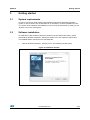
1.
Click the STEVAL-IHP005V1_Setup.exe icon. The following window opens:
Figure 6. Installation window
DocID024383 Rev 1
9/56
Getting started
2.
UM1619
In the customer information window, insert the required customer data and click “Next”.
Read the license file and click the “Yes” button if you accept the license agreement.
Figure 7. License window
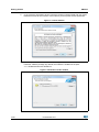
3.
In the next window, click “Install”. In the following window, select the folder in which to
install the software package. By default, the software is installed in the path:
"C:\...\STMicroelectronics\ IHP005-V1.
Figure 8. Destination folder window
10/56
DocID024383 Rev 1
UM1619
Getting started
4.
after selecting the folder and clicking the “Next” button, installation of the software
starts.
Figure 9. Installation status window
5.
When installation is complete, click “Finish”. The GUI is located in the folder “Software Remote Console 5.5”.
DocID024383 Rev 1
11/56
Hardware installation
4
UM1619
Hardware installation
Connect a regulated dual DC power supply to the power connector J2 or use the power
source pins of connector J4 as described previously and power the module.
In order to download the firmware, plug the programmer adapter (Figure 5) into the
programming connector J3 and the IAR JLink programmer in the JTAG connector of the
adapter.
Refer to Section 6: Firmware description for the firmware download procedure. As soon as
the application is launched, the LEDs should quickly switch on and off sequentially, and at
the end the orange LED should be switched on, indicating that the module needs to be
configured.
In order to configure the module, connect an RS232 DB9 female connector to one of the
available PC COM ports and the J4 connector as indicated in Figure 10.
Figure 10. RS232 connection
Run the “Remote Console for GP ST7540” GUI. Click the OPTIONS tab and select the
correct COM port from the list shown in the COM port option box (Figure 11).
In the CONFIGURATION tab, press the CONNECT button. The orange LED of the module
will flash twice and will stay switched on.
12/56
DocID024383 Rev 1
UM1619
Hardware installation
Figure 11. GUI options tab
The module is now in programming mode; the “Programing mode” message will flash at the
bottom of the interface, near the connected COM port indication.
DocID024383 Rev 1
13/56
Software GUI description
UM1619
5
Software GUI description
5.1
Introduction
The software GUI is a demonstration tool that allows to program and set up the GP power
line modules and test all the embedded features.
The GUI is composed of several tabs, each one grouping different functions. A log window
is present at the bottom of the GUI and is common to all tabs. Each operation performed by
the user, by the modules and each error are logged in this window. The decimal view check
box allows swapping of the data display from hexadecimal to decimal mode. Independent of
the visualization, each item of data can be inserted by the user in decimal or hexadecimal
mode (starting the latter with the token 0x).
5.2
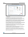
Configuration tab
This tab (Figure 12) is dedicated to the module configuration. As soon as the GUI is started
(and the COM port selected as described in the Hardware Installation paragraph), press the
CONNECT button. The module enters the programming mode, the orange LED flashes
twice and stay switched on. In the GUI the orange message “Programming Mode” flashes at
the bottom of the window.
In this tab there are several configuration panels, described hereafter.
•
Dongle Parameters
In the dongle parameters panel it is possible to assign an address to the device. The
configuration is able to group certain modules with other and form a sub network (group)
independent from other groups, sharing the same power line. If the grouping feature is used,
select the grouping box in the working mode box, and assign the same group number to
each module belonging to the same sub network. If the grouping feature is not used, the
group fields are considered as the highest part of a 6 bytes address.
The address field is a 4 bytes address of the module if the grouping is used, otherwise is the
lowest 4 byte part of a 6 bytes address if the grouping is not used.
14/56
DocID024383 Rev 1
UM1619
Software GUI description
Figure 12. GUI configuration tab
•
Working Mode
The working mode panel is used to specify the working mode of the power line
communication. The communication between two or more modules can be with or without
acknowledgment and with or without back acknowledgment. Select the respective check
box in order to enable or disable the ACK/bACk frames on a communication.
Checking the REPEATER box, the module works also as a repeater in case a data frame is
not addressed to itself. In this case, after a certain delay, if the targeted module does not
reply with an ACK to the sender, the module repeats the data frame as it was previously
sent. The repetition for a given frame is done only once per each module.
If the STATIC REPEATER check box is checked, the module repeats statically each sensed
frame without checking if the frame has been received/acknowledged or not. In both cases
the anti-collision mechanism (explained in the UM1573) is always adopted.
The GROUPING check box allows the creation of sub nets (group of modules interacting
only among those with the same group number). The group number has to be specified in
the group field of the dongle parameters panel.
The ENCRYPTION (AES128) check box enables the encryption mode: all the data
exchanged by the module are encrypted using the standard AES128 encryption algorithm.
The 128 bit encryption key is configurable in the AES key panel.
The HOP LEVEL check box allows to assign a hierarchical level to each module that is
enabled to work also as a repeater. Each time a data frame is repeated, the hop is
decremented by one. Only the modules with lowest hop level will repeat the same frame.
Please refer to user manual UM1573: ST7540 power line modem firmware stack for more
details on PLM protocol parameters.
DocID024383 Rev 1
15/56
Software GUI description
•
UM1619
AES key
The 128 bits of the AES key are set here in this panel. In order to enable the AES key panel,
before to connect the module, check the relative option USE ENCRYPTION (AES 128) in
the option tab.
•
Dongle description
This box is used to associate a description of the programmed module to the node address.
The description together with the module will be displayed everywhere in the GUI each time
a node list is displayed. The description is stored in a local database, so if you run the GUI
with a programmed node in another PC, the description is missing. The node list file is
located in the directory C:\Program Data\STMicroelectronics\Remote
Console\1.0.0.0\settings\donglelist.l
It is possible to manually edit this file using a text editor, adding in each line the following
text:
0xg1.0xg0.0xa3.0xa2.0xa1.0xa0 -> description
where g1 and g0 are the group byte values (in hexadecimal) and the a3, a2, a1 and a0 are
the address byte values (in hexadecimal). The description is what will appear in the dongle
description panel and in all node list of the GUI.
•
Hardware
In the hardware panel there are the connection and disconnection buttons. As soon as the
CONNECT button is pressed, if the module is connected the “Programming Mode” message
will flash at the bottom of the window, and the module enters programming mode. The
disconnect button disconnects the GUI from the COM port.
•
Dongle mode
As soon as the module is connected, the two buttons RUN and PROGRAM of the dongle
mode panel switches the module modes respectively in run mode and in programming
mode.
•
Commands
In the commands panel the SET button is used to download the chosen configuration
described previously, while the GET button is used to get the configuration present in the
module. If a module has never been programmed before, the group and the address field
are filled with 0xFF values and the run button will not have an effect.
As soon as the module is in run mode, the set to remote address button is enabled. This
button is used to configure a remote node connected via power line, working in the same
manner as the SET button. This procedure has effect only if the node has never been
programmed before (or if the remote address is set to 0xFF both in the group and address
box). Of course, only one module must be present with this address in the same power line,
otherwise the selected configuration (and the chosen new address and group) will be
assigned to each of these nodes.
16/56
DocID024383 Rev 1
UM1619
Software GUI description
If the module (dongle) is in programming mode, all the other tabs are locked. In order to
unlock all the tabs, press the RUN button. The GUI and the module will enter in run mode,
and the run mode message will appear in green at the bottom of the window. The module
LED will be switched off.
5.3
Dongle tab
The DONGLE tab (Figure 13) is where to set up and use two features embedded in the
module, the real-time clock (RTC), and the general purpose inputs/outputs pins.
The node time indicates the value of the internal RTC of the module. Press the GET TIME
button in the commands panel to know the actual time of the module. In order to modify the
time, write the new time in the node time panel and click the SET TIME button. The module
time can be synchronized with the PC time shown in the current time panel. In this case,
simply check the SET CURRENT option in the node time panel before pressing the SET
TIME button.
The module has 8 general purpose input/output pins that can be configured individually
either as input pin or as output pin. In order to know the actual configuration, press the GET
IO CFG button in the commands panel. If a pin is configured as input, the Input x (where x is
the number of the pin) appears in the input status panel with the respective check box
checked, and a red or a green LED is shown. the color of the LED specifies if in the module
pin is applied a high level (+3.3 V), in this case the LED is red, or a low level (GND) in this
case the LED is green.
If the pin is configured as output, the output x (where x is the pin number) is shown in the
input status panel, and the corresponding check box is unchecked. A toggle pushbutton is
than associated to each output, indicating if the correspondent pin in the module must be
set high (+3.3 V), in this case the pushbutton must be pressed before to press the set
outputs button in the commands panel, or must be set low (GND) releasing the pushbutton
before press the set outputs button in the commands panel.
DocID024383 Rev 1
17/56
Software GUI description
UM1619
Figure 13. GUI dongle tab
As soon as the pin configuration is set by the user (checking or unchecking the
corresponding check box), the SET IO CFG button must be pressed before the
configuration has effect. After that, each output can be set/reset and each input can be
checked.
All those operations can be done in different way: in broadcast mode, in this case if the
BROADCAST check box in the commands panel is selected before press any button, each
“set” operation will be executed by each node connected in the same power line. The
command will be sent by the module connected to the GUI via the power line to all the other
nodes. In order to configure a single node (a remote node or the one connected to the GUI),
the node must be selected in the AVAILABLE NODE LIST window before to press any
command button. In broadcast mode the get operations are not allowed.
Last, the STOP button resets the connected dongle if some remote operations are ongoing
and the user wants to interrupt the operation.
Be aware that the I/O pins are not protected and directly wired with the microcontroller Poi's
pins. So if the pins are electrically connected in a wrong way a serious damage can be
caused in the module.
5.4
Operations tab
The OPERATIONS tab (Figure 14) is the place where to test a communication between two
modules connected to the same power line. In the Message window is possible to write a
text message, select the target node in the available node list, and send the message by
pressing the SEND MSG button.
18/56
DocID024383 Rev 1
UM1619
Software GUI description
Figure 14. GUI operations tab
If the message has to be sent in broadcast, the BROADCAST check box must be checked.
As soon as the send message is sent, the green LED of the module connected to the GUI is
switched on. When the LED is switched off the message has been sent to the target module
or an error has occurred. The operation result is shown in the log window.
If the target device is connected to a PC with a running GUI, the received message is shown
in the log window.
DocID024383 Rev 1
19/56
Software GUI description
5.5
UM1619
Program tab
The PROGRAM tab shown in Figure 15 is used to store permanently user data in the
module flash memory. Actually is possible to store 20 bytes as example, but modifying a
constant in the firmware (#define USER_SETTINGS_SIZE directive) in the interfaceconfig.h
file it is possible to store more then 800 bytes of user data.
Figure 15. GUI program tab
As previously described for other features, the command to store data can be sent in
broadcast or to a precise module listed in the AVAILABLE NODE LIST window by pressing
the SET button.
The get button instead reads the stored data from the selected node.
20/56
DocID024383 Rev 1
UM1619
5.6
Software GUI description
Service tab
The SERVICE tab is shown in Figure 16. This tab is dedicated to the test of all the special
frames called service frames. The first button in the commands panel is the PING button.
This is used to test if a module is connected to the power line, if it is working properly and if
it is reachable.
By pressing the PING button, as soon as the target module replies to the ping command,
the target address and the ping time are shown in the Command window.
Figure 16. GUI service tab
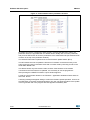
In order to know the firmware release both for the application layer and the link layer stack,
the FIRM. REL. button must be pressed after selecting the target node in the AVAILABLE
NODE LIST. Both the releases are then shown in the command window.
It is possible to modify some parameters that fine-tune the power line modem
communication protocol. This operation can affect the overall communication performance,
so it must be done with great attention. Please refer to UM1573 for a detailed description of
the communication protocol parameters.
Select the node for which the parameters should be checked or modified, then press the
PLM PARAM button. A windows prompting to insert a password appears. Insert the
password “syslab” and then press the Enter key.
A list of the available communication parameters appears at the right side of the GUI,
overlapping the available node list, with three buttons at the bottom side (Figure 17).
In order to know the preset PLM communication parameters, press the GET button.
DocID024383 Rev 1
21/56
Software GUI description
UM1619
Figure 17. PLM communication parameters window
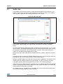
By default, the PLM is configured to work properly. Pressing the DEFAULT button, the
parameter boxes are populated with the default values. Modify with care each parameter,
and press the SET button to send the parameters to the addressed node (the selected node
is shown in the top of the parameter window).
The UPDATE FW button implements the remote firmware update feature (RFU).
The RFU allows the user to update the firmware of a module connected remotely in the
same power line, both in broadcast mode and in unicast mode by selecting a node in the
AVAILABLE NODE LIST.
This feature works only with remote nodes, because if the firmware of the module
connected to the GUI needs to be updated, it is necessary to use the programmer.
After pressing the UPDATE FW button a open window appears.
Locate the new firmware release in the Firmware - Application standalone folder and then
select the .bin file.
A warning message will appear asking to confirm the firmware update operation. As soon as
the YES button is pressed, the download starts. The user can follow the status of the update
in the log window and in the progress bar that appears immediately after.
22/56
DocID024383 Rev 1
UM1619
5.7
Software GUI description
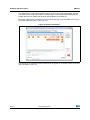
Sniffer tab
It is possible to use the GUI interface to check the data transiting on the power line. This
feature is useful when the PLM protocol parameters are tuned. By “sniffing” the transiting
data it is easy to determine the overall performance of the network.
Figure 18. GUI sniffer tab
Before using the sniffer feature, it is necessary to download into a GP PLM module the
sniffer binary code provided in the setup packet, and located in the folder “Firmware Sniffer”.
Open the IAR Embedded Workbench® IDE for STM32 microcontrollers Rel. 6.3 (or a more
recent release), click File\Open\Workspace and select the workspace Flasher.eww. Connect
the Jlink/Jtrace programmer into the programming connector of the module and press
CTRL+D or click Project\Download & Debug option.
Note that as soon as the sniffer bin file is downloaded in the module, it will work only as a
sniffer.
Connect the sniffer module to an available COM port of the PC, open the GUI and select the
SNIFFER tab. Click on the button START to start the data sniffing.
Normally the data sniffed in the power line is also saved in a snifflog file. This feature can be
disabled just unchecking the SAVE TO FILE checkbox. The file is located in the folder:
C:\Program Data\ST Microelectronics\Remote Console\1.0.0.0\settings\snifflog.txt
and as soon as the sniffing activity is completed it can be renamed and stored in a different
location. The GUI will create another sniffer file as soon as the start button is pressed again
and the SAVE TO FILE option is checked.
The snifflog.txt file can be read with any text editor, and can be automatically erased from
the GUI by pressing the DELETE LOG FILE button.
DocID024383 Rev 1
23/56
Software GUI description
UM1619
The STOP button stops data acquisition without to losing previously sniffed data, appends
new data as soon as the start button is pressed again. The CLEAR button deletes all the
sniffed data from the sniffer main window, without deleting the sniffer file.
Each time a data frame is sniffed, the log window is filled with some information concerning
the sniffed frame as shown in the Figure 19.
Figure 19. Sniffer information
The following is a description of the symbols that can appear in the sniffer window, indicated
with a number in Figure 19.
24/56
DocID024383 Rev 1
UM1619
Software GUI description
1.
As soon as the START button is pressed the sniffing date and time is shown. Each time
a data frame is received this number represents the time passed (in seconds) after the
previous received data frame.
2.
This symbol represents the frame type, and can be one of the following:
–
DAT: Data frame
–
SER: Service frame
–
PNG: Ping frame
–
ERR: Error frame
–
PRG: Programming frame
–
ACK: Acknowledge frame
–
BAK: Back acknowledgment frame
–
UNK: Unknown frame type
–
*P*: Frame rejected because a wrong postamble
–
*C*: Frame rejected because a wrong CRC
3.
S:0x...: Sender device address (without group indication)
4.
D:0x...: Target device (destination) address (without group indication)
5.
Frame sent in Unicast (-U) or Broadcast (+B)
6.
Frame with acknowledgment required (+A) or not required (-A)
7.
Frame with back acknowledgment required (+b) or not required (-b)
8.
Frame can be repeated (+R) or repeating disable for that frame (-R)
9.
Normal repeating mode (-n) or static repeating mode (+s)
10. Grouping enabled (+G) or disabled (-G)
11. Data not encrypted (-E) or encrypted data (+E)
12. ID:xxx Indicates the frame ID number (xxx)
13. FEC: nnn Represents the number of the FEC (forward error check) correction for that
data frame. This is done by the sniffer device, giving an idea of the line noise in the
around where the sniffer is placed. The FEC algorithm is the same as the one
implemented in the module firmware
14. LEN:yyy Indicates the user data payload length
15. HOP: hhh This is the hop level of the received data frame
DocID024383 Rev 1
25/56
Firmware description
UM1619
6
Firmware description
6.1
Introduction
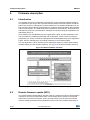
The firmware structure is constituted of several layers, each managing a different feature.
The application layer engine is the general interface between the user program and all the
parts of the module. It manages the communication ports, the module peripherals such as
RTC and I/Os, LEDs and timing management. It is also the interface between the PLM stack
and the user program. The PLM stack, itself constituted of several layers, implements and
manages the power line communication, manages the conflicts, timing and repetitions, the
addressing and so on.
Some features are managed directly by the application engine, and are transparent to the
user, as well as the module programming and configuration, which is done by particular
programming or service commands managed and acknowledged directly by the application
engine, the RTC management, the module parameter or the firmware update.
The user application can be interfaced to the application engine by simples APIs used for
the data transfer and the module interfacing. The Figure 20 shows the firmware structure.
Figure 20. Module firmware structure
The user program is located in the user.c and user.h file in the application project.
6.2
Remote firmware update (RFU)
The remote firmware update (RFU) uses the power line modem as external communication
channel for receiving a new firmware dump. The firmware dump is placed in the internal
flash memory of the microcontroller. Hence, the total memory size of the microcontroller
must be at least the double of the estimated maximum size of the firmware application (in
26/56
DocID024383 Rev 1
UM1619
Firmware description
this application is set to 60 Kbytes), plus 4 Kb of additional memory for a bootloader.
Figure 21 shows the microcontroller memory organization.
The bootloader is loaded at startup and checks the active segment containing the actual
firmware. The implemented mechanism uses three partitions of the microcontroller's Flash
memory, one containing the bootloader and two containing the actual running firmware
(active image) and the new firmware as soon as a RFU is needed.
As soon as the firmware transfer is completed, a “swap” command sent from the remote
PLM causes the target PLM to check first the integrity of the firmware dump (actually a
checksum is calculated and compared with the one sent by the remote PLM), and after the
reset vector address of the new firmware is written in a dedicated Flash segment of the
bootloader. Lastly, the microcontroller is self-reset, and the new firmware executed.
Figure 21. Memory organization
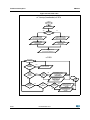
The RFU protocol manages the RFU “start”, “get new firmware segment” (with the segment
address) and “swap” commands. The protocol is not embedded in the bootloader, hence it
can be updated with the new firmware, but the user must be careful with the modifications,
as any bug can compromise the RFU mechanism.
As soon as a new firmware segment is received, the RFU manager checks if the address is
within the firmware interrupt vector table. If it is the case, an offset depending on the free
firmware image (1 or 2) allocation is added to each interrupt vector before being written in
the free image flash area.
Figure 22 shows the RFU flow chart.
DocID024383 Rev 1
27/56
Firmware description
UM1619
Figure 22. RFU flow chart
V$4UBSUVQCPPUMPBEFS
V$3'6
X&
67$5783
5($'$&7,9(
,0$*($''5(66
<(6
12
),567,0$*(
$''5(66"
/2$'67$&.32,17(5
5(*,67(5:,7+),567
9(&7257$%/($''5(66
/2$'67$&.32,17(5
5(*,67(5:,7+6(&21'
9(&7257$%/($''5(66
/2$'9(&7257$%/(
5(*,67(5:,7+),567
9(&7257$%/(
/2$'9(&7257$%/(
5(*,67(5:,7+6(&21'
9(&7257$%/(
-80372
1(:$33/,&$7,21$''5(66
9(&7257$%/(5(*,67(5
V$3'6
$33/,&$7,21
5811,1*
5)867$57
&200$1'
5(&(,9('"
<(6
6725(&+(&.680
6725(727$/6,=(
12
1(:
),50:$5(
6(*0(17
5(&(,9('"
<(6
),567
,0$*(,6
$&7,9("
<(6
6725(6(*0(17,17+(
6(&21',0$*($77+(
*,9(1$''5(66
2))6(7,6$''(',17+(
9(&7257$%/(
6725(6(*0(17,17+(
),567,0$*($77+(
*,9(1$''5(66
12
12
X&
5(6(7
2))6(7,6$''(',17+(
9(&7257$%/(
12
5)86:$3
&200$1'
5(&(,9('"
<(6
&+(&.680
,6
&255(&7"
<(6
),567
,0$*(,6
$&7,9("
12
12
28/56
DocID024383 Rev 1
<(6
6725(7+(6(&21'
,0$*($'5(66,17+(
%227/2$'(5'$7$
6(*0(17
6725(7+(),567
,0$*($'5(66,17+(
%227/2$'(5'$7$
6(*0(17
UM1619
6.3
Firmware description
Firmware download
In the setup directory there are different workspaces stored in different directories. In order
to implement the remote firmware update feature it is necessary to download the project
located in the workspace “Firmware - Application and Bootloader”. This workspace contains
two different projects, one is the bootloader and the other one is the application itself. If the
module has never been programmed, this workspace must be downloaded before.
Open the IAR Embedded Workbench® IDE for STM32 microcontrollers Rel. 6.3 (or a more
recent release). Click File\Open\Workspace and load the following workspace placed in the
directory selected during the setup file installation: “Firmware - Application and
Bootloader\EWARM\Project.eww”. Verify that the Application project is the active project
(the project name must be in bold), otherwise select the active project in the list below the
workspace (Figure 23).
Figure 23. Active project selection
Click “Project - Batch Build” or press the key F8 in order to compile at the mean time the
bootloader and the application.
After compiling is completed, press “Project - Download and Debug” or press CTRL+D keys.
Both firmware downloads start. As soon as the download is completed, press F5 in order to
run the application (or exit from the debug mode pressing the keys CTRL+SHIFT+D and
unplug the programmer).
If the procedure is done correctly, the orange LED should be on, indicating the module has
never been set up before. If it is not the case, try first to erase the memory by clicking
Project\Download\Erase Memory and download the firmware again as described previously.
Use the GUI interface in order to set up the module and connect it to the power line as
described in the dedicated paragraph.
As soon a bootloader has been installed in the module it is possible to remotely (via power
line) update the firmware using the RFU feature. Each new firmware version has to be
programmed using the workspace “Firmware - Application
standalone\EWARM\Project.eww”. The bin file produced by this workspace that is located in
the folder “Firmware - Application standalone\ EWARM\PLM_HID_STANDALONE.bin” can
be directly loaded using the GUI interface. The difference of this application with the one
contained in the workspace with the bootloader is mainly in the stm32f10x_flash.icf linker file
and some workspace parameters that are not used in the application without the bootloader
(as multiple build, simultaneous debug mode, etc.).
DocID024383 Rev 1
29/56
Firmware description
UM1619
The setup folder contains also the Firmware - Bootloader folder, where inside there is the
bootloader firmware; and the folder Firmware - Sniffer which contains the sniffer workspace
to download in a PLM module useful if the data sniffing feature of the interface is used. In
this case the PLM module will work only as a sniffer.
6.4
Firmware description
The structure of the workspace is divided in different sections as shown in the Figure 24.
The user program must be developed in the user.c and user.h files.
Figure 24. Workspace structure
^LJƐƚĞŵĨŝůĞƐ
W>DĚƌŝǀĞƌ
ƉƉůŝĐĂƚŝŽŶŶŐŝŶĞ
hƐĞƌůĂLJĞƌ
^dDϯϮ^ƚĂŶĚĂƌĚůŝďƌĂƌLJ
30/56
DocID024383 Rev 1
UM1619
Firmware description
At this level are available all the communication APIs and all the APIs for the application
engine interfacing.
In the main file, the following code is implemented for running the state machine engines:
main(void)
{
/* System initialization */
APP_ApplicationInit();
/* Infinite loop */
while (1)
{
/* USER program execution, defined in “user.c” and “user.h” files */
USER_Program();
/* Application stack engine */
APP_StackUpdate();
}
}
After the initialization the infinite loop calls two main functions: the USER_Program() and the
APP_StackUpdate() routine. The latter is the application engine state machine which inside
runs the PLM stack state machine, while the first one calls the user program.
The user program implemented in this user manual implements a bridge between the power
line communication and the COM port: each data received from the COM port addressed to
another PLM module is sent via PLM, and vice-versa each data received from PLM is sent
back to the COM port. It is necessary that the user program does not stop the core
operations (looping instructions) without calling the application engine.
All the firmware configurations are contained in the interfaceconfig.h file. Here the user can
define the default working mode and all the default values of the module parameters.
The following paragraphs list all the data types and the APIs used in the application engine,
that can be modified by the user if different needs arise.
DocID024383 Rev 1
31/56
Firmware description
6.5
UM1619
Firmware data types
The data type found in the application.h module, are listed below:
/* USER FRAME STRUCTURE */
typedef struct
{
APP_source_t source;
APP_ftype_t
type;
bool
broadcast;
u16
group;
u32
address;
u8
len;
u8
data[USER_PAYLOAD_SIZE]; /* MAX PAYLOAD SIZE: 100 bytes */
APP_ERROR_t
error;
}APP_userdata_t;
/* PERIPHERAL SOURCE TYPE */
typedef enum
{
SOURCE_COMM,
SOURCE_USB,
SOURCE_SPI,
SOURCE_PLM
}APP_source_t;
/* APPLICATION FRAME TYPE */
typedef enum
{
APP_DATA_FRAME
= 0x00,
APP_SERVICE_FRAME
= 0x01,
APP_PING_FRAME
= 0x02,
APP_ERROR_FRAME
= 0x03,
APP_PROGRAMMING_FRAME
= 0x04,
APP_ACK_FRAME
= 0x05
/* <!> MAX ALLOWED TYPE RANGE: FROM 0x00 TO 0x7F */
}APP_ftype_t;
/* APPLICATION ERRORS */
typedef enum
{
APP_ERROR_NONE
APP_ERROR_GENERIC
APP_ERROR_COMM_TIMEOUT
APP_ERROR_SERVICE_GRP_UNKNOWN
APP_ERROR_SERVICE_CMD_ERROR
APP_ERROR_COMMUNICATION
APP_ERROR_ISOLATED_NODE
APP_ERROR_HARDWARE
APP_ERROR_WRONG_PROG_COMMAND
APP_ERROR_WRONG_PROG_GROUP
APP_ERROR_DEVICE_BLANK
APP_ERROR_RTC_ERROR
APP_ERROR_WATCHDOG_DISABLED
APP_ERROR_NODE_INIT_FAILED
APP_ERROR_RTC_DISABLED
}APP_ERROR_t;
=
=
=
=
=
=
=
=
=
=
=
=
=
=
=
0x00,
0x01,
0x02,
0x03,
0x04,
0x05,
0x06,
0x07,
0x08,
0x09,
0x0a,
0x0b,
0x0c,
0x0d,
0x0e
/* USER COMMUNICATION FLAGS */
typedef enum
{
USER_DATA_TRANSMISSION_START,
USER_DATA_TRANSMISSION_END,
USER_DATA_ARRIVED,
USER_DATA_COMMUNICATION_ERROR,
32/56
DocID024383 Rev 1
//
//
//
//
//
//
//
//
//
//
//
//
//
//
//
No error
Generic communication error
Communication timeout error
Service group unknown error
Service command error
Communication error
Node unreachable error
Hardware error
Wrong programming command error
Wrong programming group error
Device blank
Error setting the system time
Hardware reset impossible
Node initialization failure
Internal RTC disabled
UM1619
Firmware description
USER_DATA_BUSY,
USER_DATA_IDLE
}APP_userflag_t;
/* PROGRAMMING COMMANDS */
typedef enum
{
PROG_CMD_IDLE
PROG_CMD_ENTER_PROG_MODE
PROG_CMD_EXIT_PROG_MODE
PROG_CMD_SET_DATA
PROG_CMD_GET_DATA
PROG_CMD_CLEAR_DATA
PROG_CMD_DEVICE_BLANK
}APP_PROG_CMD_t;
/* PROGRAMMING GROUPS */
typedef enum
{
PROG_GRP_DEVICE_DATA
PROG_GRP_LL_STACK_PARAM
PROG_GRP_USER_DATA
}APP_PROG_GROUP_t;
=
=
=
=
=
=
=
0x00,
0x01,
0x02,
0x03,
0x04,
0x05,
0x06
= 0x00,
= 0x01,
= 0x02
//
//
//
//
//
//
//
No command
Enter the programming mode
Exit from programming mode
Write data into the internal flash
Get data from internal flash
Clear data resetting the programming flag
Device blank: run mode impossible
// Device Data
// Link layer stack parameters
// User program
/* SERVICE COMMANDS */
typedef enum
{
/* NATIVE SERVICE COMMANDS */
SERVICE_SOFTWARE_RESET
= 0x00,
SERVICE_HARDWARE_RESET
= 0x01,
SERVICE_PARAM_SET
= 0x02,
SERVICE_PARAM_GET
= 0x03,
SERVICE_INPUTS_GET
= 0x04,
SERVICE_OUTPUTS_SET
= 0x05,
SERVICE_FW_REL_GET
= 0x06,
SERVICE_PLM_CLOCK_SET
= 0x07,
SERVICE_PLM_CLOCK_GET
= 0x08,
SERVICE_IO_CONFIG_SET
= 0x09,
SERVICE_IO_CONFIG_GET
= 0x0a
/* USER DEFINED SERVICE COMANDS */
// SERVICE_USER_CMD_xx
= 0x..,
}APP_SER_CMD_t;
//
//
//
//
//
//
//
//
//
//
//
Reset internal state machines
Module hardware reset
Set service parameters
Get service parameters
Get general purpose inputs pin status
Set general purpose outputs pins value
Get the stack and the module firmware release
Set the internal time clock value
Get the internal time clock value
Set the general purpose input and output pins
Get the general purpose input and output pins
// User defined service commands (0x0b to 0x7f)
/* TRANSIT DATA SERVICE FLAGS */
typedef struct
{
APP_TF_t type;
uint8_t
FECcorrections;
bool
wrongpostamble;
bool
wrongCRC;
bool
hopoverrun;
bool
framerejected;
}APP_SER_FLAGS_t;
//
//
//
//
//
Number of FEC correction to the sensed frame
Frame with for a wrong postamble
Frame with a wrong CRC
Frame with a HOP overrun
TRUE = Frame rejected, FALSE = frame accepted
//
//
//
//
//
//
//
//
//
Data
Error
Programming
Result (response to a query, same as data frame)
ACK
back ACK
Ping
Service
Unknown type
/* TRANSIT FRAME TYPE */
typedef enum
{
APP_TF_DATA
APP_TF_ERROR
APP_TF_PROGR
APP_TF_RES
APP_TF_ACK
APP_TF_bACK
APP_TF_PING
APP_TF_SERVICE
APP_TF_UNKNOWN
=
=
=
=
=
=
=
=
=
0x00,
0x01,
0x02,
0x03,
0x04,
0x05,
0x06,
0x07,
0x7f
}APP_TF_t;
DocID024383 Rev 1
33/56
Firmware description
UM1619
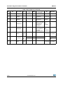
The data type for the “dongle.h” module; “stm32f10x_gpio” module are listed hereafter:
/* LED TYPE */
typedef enum
{
A_LED_ERROR,
A_LED_DATA,
A_LED_BOTH
}DH_LedType_t;
/* LED STATUS */
typedef enum
{
A_LED_ON,
A_LED_OFF,
A_LED_FLASH
}DH_LedAction_t;
/* PIN VALUE */
typedef enum
{
Bit_RESET = 0,
Bit_SET
}BitAction;
6.6
Firmware frame types
This paragraph describes all the frame type that are implemented in this firmware. In each
field there is also a description.
6.6.1
Data Frames
Data frames are frames exchanged between two PLM modules or between a PLM module
and an external device connected to the COMM interface.
From the COMM interface module (SPI, USART, USB etc.)
buffer[0] = n + 10;
buffer[1] = APP_DATA_FRAME | BROADCAST_FLAG;
buffer[2,3] = target_module.group;
buffer[4,5,6,7] = target_module.address;
buffer[8,..8+n-1] = user_data[n];
buffer[8+n,8+n+1] = CRC16;
//
//
//
//
//
//
Data frame payload length (n + 10)
Data frame type
Target device group (2 bytes)
Target device address (4 bytes)
User data (n bytes, at least 1)
CRC-16
/* BROADCAST_FLAG = 0x80 -> data sent in broadcast - BROADCAST_FLAG = 0x00 -> data sent in
unicast */
From / to communication interface (PLM, SPI, USART, USB, etc.)
frame.source = SOURCE_PLM / ...;
frame.type = APP_SERVICE_FRAME;
frame.len = n;
frame.broadcast = TRUE / FALSE;
frame.group = target_module.group;
frame.address = target_module.address;
frame.data[n] = service_data[n];
34/56
DocID024383 Rev 1
//
//
//
//
//
//
//
Data source PLM, ...
Data frame type
Data frame payload length
TRUE = broadcast, FALSE = unicast
Target device group (2 bytes)
Target device address (4 bytes)
User data (n bytes)
UM1619
6.6.2
Firmware description
Ping Frames
This particular frame is used to ping a remote (via PLM interface) or a local (via COMM
interface) module. When a ping frame is received, this is managed directly at data link layer
and is not notified at the application and consequently at the user levels.
From the COMM interface module (SPI, USART, USB, etc.)
buffer[0] = 10;
buffer[1] = APP_PING_FRAME;
buffer[2,3] = target_module.group;
buffer[4,5,6,7] = target_module.address;
buffer[8,9] = CRC16;
//
//
//
//
//
Ping frame payload length (n + 11)
Ping frame type
Target device group (2 bytes)
Target device address (4 bytes)
CRC-16
From / to communication interface (PLM, SPI, USART, USB, etc.)
frame.source = SOURCE_PLM / ...;
frame.type = APP_PING_FRAME;
frame.len = 0;
frame.broadcast = FALSE;
frame.group = target_module.group;
frame.address = target_module.address;
6.6.3
//
//
//
//
//
//
Data source PLM, ...
Ping frame type
Ping frame payload length
Ping frames can be sent only in unicast
Target device group (2 bytes)
Target device address (4 bytes)
Error Frames
These can be considered data frames; they are user error frames from user application level
addressed to a target PLM module.
From the COMM interface module (SPI, USART, USB, etc.)
uint8_t *buffer;
buffer[0] = 12;
buffer[1] = APP_ERROR_FRAME;
buffer[2,3] = target_module.group;
buffer[4,5,6,7] = target_module.address;
buffer[8,9] = user_error_code;
buffer[10,11] = CRC16;
//
//
//
//
//
//
Error frame payload length (12)
Data frame type
Target device group (2 bytes)
Target device address (4 bytes)
User error code (2 bytes)
CRC-16
From / to communication interface (PLM, SPI, USART, USB, etc.)
APP_userdata_t frame;
frame.source = SOURCE_PLM / ...;
frame.type = APP_ERROR_FRAME;
frame.len = 2;
frame.broadcast = FALSE;
frame.group = target_module.group;
frame.address = target_module.address;
frame.data[0,1] = user_error_code;
//
//
//
//
//
//
//
Data source PLM, ...
Error frame type
Error frame payload length
Error frames are sent in unicast
Target device group (2 bytes)
Target device address (4 bytes)
User error code (2 bytes)
Error code list
0x00
0x01
0x02
0x03
0x04
0x05
0x06
0x07
0x08
0x09
0x0a
0x0b
0x0c
0x0d
0x0e
=
=
=
=
=
=
=
=
=
=
=
=
=
=
=
APP_ERROR_
APP_ERROR_GENERIC
APP_ERROR_COMM_TIMEOUT
APP_ERROR_SERVICE_GRP_UNKNOWN
APP_ERROR_SERVICE_CMD_ERROR
APP_ERROR_COMMUNICATION
APP_ERROR_ISOLATED_NODE
APP_ERROR_HARDWARE
APP_ERROR_WRONG_PROG_COMMAND
APP_ERROR_WRONG_PROG_GROUP
APP_ERROR_DEVICE_BLANK
APP_ERROR_RTC_ERROR
APP_ERROR_WATCHDOG_DISABLED
APP_ERROR_NODE_INIT_FAILED
APP_ERROR_RTC_DISABLED
DocID024383 Rev 1
35/56
Firmware description
6.6.4
UM1619
Acknowledgment Frames
These frames are particular data frames sent to an external device connected to the COMM
module, not allowed to be sent via PLM. They are used by the GUI interface to acknowledge
the commands sent to the module.
From the COMM interface module (SPI, USART, USB, etc.)
uint8_t *buffer;
buffer[0] = 12;
buffer[1] = APP_ACK_FRAME;
buffer[2,3] = target_module.group;
buffer[4,5,6,7] = target_module.address;
buffer[8] = (APP_ftype_t)ack_group_type;
buffer[9] = command_echo;
buffer[10,11] = CRC16;
//
//
//
//
//
//
//
Error frame payload length (12)
ACK frame type
Target device group (2 bytes)
Target device address (4 bytes)
Frame type to acknowledge
Acknowledged command echo
CRC-16
From / to communication interface (PLM, SPI, USART, USB, etc.)
APP_userdata_t frame;
frame.source = SOURCE_PLM / ...;
frame.type = APP_ACK_FRAME;
frame.len = 2;
frame.broadcast = FALSE;
frame.group = target_module.group;
frame.address = target_module.address;
frame.data[0] = (APP_ftype_t)ack_group_type;
frame.data[1] = command_echo;
6.6.5
//
//
//
//
//
//
//
//
Data source PLM, ...
ACK frame type
ACK frame payload length
ACK frames are sent in unicast
Target device group (2 bytes)
Target device address (4 bytes)
Frame type to acknowledge
Acknowledged command echo
(service, programming, ...)
Programming Frames
Programming frames are used to program the PLM module parameters, as the static
address, the AESkey (if encryption is used), the data link stack working model and to clear
or read programming parameters. Normally these commands are sent locally to the module
from an external device connected to the COMM peripheral (SPI, USART, USB, etc.).
From the COMM interface module (SPI, USART, USB, etc.)
uint8_t *buffer;
buffer[0] = n + 11;
buffer[1] = APP_PROGRAMMING_FRAME;
buffer[2,3] = target_module.group;
buffer[4,5,6,7] = target_module.address;
buffer[8] = (APP_PROG_CMD_t)command;
buffer[9,..9+n-1] = programming_data[n];
buffer[9+n,9+n+1] = CRC16;
//
//
//
//
//
//
//
Programming frame payload length (n + 11)
Programming frame type
Target device group (2 bytes)
Target device address (4 bytes)
Programming command
Programming data
CRC-16
From / to communication interface (PLM, SPI, USART, USB, etc.)
APP_userdata_t frame;
frame.source = SOURCE_PLM / ...;
frame.type = APP_PROGRAMMING_FRAME;
frame.len = n + 1;
frame.broadcast = TRUE / FALSE;
frame.group = target_module.group;
frame.address = target_module.address;
frame.data[0] = (APP_PROG_CMD_t)command;
frame.data[n] = programming_data[n];
Programming commands list
0x01 = PROG_CMD_ENTER_PROG_MODE
36/56
DocID024383 Rev 1
//
//
//
//
//
//
//
//
Data source PLM, ...
Programming frame type
Programming frame payload length
TRUE = broadcast, FALSE = unicast
Programming device group (2 bytes)
Programming device address (4 bytes)
Programming command
Programming data
UM1619
Firmware description
0x02
0x03
0x04
0x05
0x06
=
=
=
=
=
PROG_CMD_EXIT_PROG_MODE
PROG_CMD_SET_DATA
PROG_CMD_GET_DATA
PROG_CMD_CLEAR_DATA
PROG_CMD_DEVICE_BLANK
1) Enter in programming mode
uint8_t *buffer;
buffer[0] = 11;
buffer[1] = APP_PROGRAMMING_FRAME;
buffer[2,3] = target_module.group;
buffer[4,5,6,7] = target_module.address;
buffer[8] = CMD_ENTER_PROG_MODE;
buffer[9,10] = CRC16;
2) Exit from programming mode
uint8_t *buffer;
buffer[0] = 11;
buffer[1] = APP_PROGRAMMING_FRAME;
buffer[2,3] = target_module.group;
buffer[4,5,6,7] = target_module.address;
buffer[8] = PROG_CMD_EXIT_PROG_MODE;
buffer[9,10] = CRC16;
3) Set module parameters: data link stack parameters
uint8_t *buffer;
buffer[0] = 62;
buffer[1] = APP_PROGRAMMING_FRAME;
buffer[2,3] = target_module.group;
buffer[4,5,6,7] = target_module.address;
buffer[8] = PROG_CMD_SET_DATA;
buffer[9] = PROG_GRP_LL_STACK_PARAM;
/* STACK PARAMETERS */
buffer[10,11] = PLM_MIN_SLOT;
buffer[12,13] = PLM_MAX_SLOT;
buffer[14,15] = PLM_NTW_P_GLOBAL_TX_TO;
buffer[16,17,18,19] = PLM_NTW_P_BC_GLOBAL_TX_TO;
//
//
//
//
buffer[20,21] = PLM_NTW_P_ACTIVITY_TO;
buffer[22,23] = PLM_NTW_P_WATCHDOG_TO;
buffer[24,25,26,27] = PLM_NTW_P_DATATRANSFER_TO;
buffer[28,29] = PLM_NTW_P_BANDINUSE_TO;
buffer[30,31,32,33] = PLM_NTW_P_FRAME_TX_TO;
buffer[34,35,36,37] = PLM_NTW_P_BCAST_TX_TO;
buffer[38,39,40,41] = PLM_NTW_P_ACK_RX_TO;
buffer[42,43,44,45] = PLM_NTW_P_bACK_RX_TO;
buffer[46,47,48,49] = PLM_NTW_P_FRM_RX_TO;
buffer[50,51,52,53] = PLM_NTW_P_NDX_TO;
buffer[54,55] = PLM_LL_MAX_ATTEMPT;
buffer[56,57] = PLM_LL_MAX_RPT_ATTEMPT;
buffer[58,59] = DEVICE_TIME_SYNC;
buffer[60,61] = CRC16;
//
//
//
//
//
//
//
//
//
Minimum backoff time
Maximum backoff time
Timeout for global tx
Timeout for broadcast frame
retransmission
// Timeout for network
// Watchdog timeout
// Timeout for completing a transfer
from source to target
// Timeout for the band in use
signal
Timeout for sending a frame through SPI
Timeout for repeat a broadcast frame
Timeout for receiving an ACK frame
Timeout for receiving a bACK frame
Timeout for frame receptions
Minimum delay before any
Max attempts if no activity is detected
Max repetition attempts (for processed ID)
Timeclock update synchro frame interval
4) Set module parameters: programming module parameters
uint8_t *buffer;
/* IF AES ENCRYPTION IS ENABLED */
buffer[0] = 36;
/* IF AES ENCRYPTION IS DISABLED */
buffer[0] = 20;
buffer[1] = APP_PROGRAMMING_FRAME;
buffer[2,3] = target_module.group;
buffer[4,5,6,7] = target_module.address;
buffer[8] = PROG_CMD_SET_DATA;
DocID024383 Rev 1
37/56
Firmware description
UM1619
buffer[9] = PROG_GRP_LL_STACK_PARAM;
buffer[10,11] = new_group;
buffer[12,13,14,15] = new_address;
buffer[16] = (uint8_t)module_working_mode;
buffer[17] = hop_level;
/* IF AES ENCRYPTION IS ENABLED */
buffer[18 -> 33] = *AES_key_buffer;
buffer[34,35] = CRC16;
/* IF AES ENCRYPTION IS DISABLED */
buffer[18,19] = CRC16;
module_working_mode
------------------------b7 b6 b5 b4 b3 b2 b1 b0
------------------------| | | | | | | +-| | | | | | +----| | | | | +-------| | | | +----------| | | +-------------| | |
| | +----------------| +-------------------+-----------------------
1
1
1
1
1
=
=
=
=
=
// AES Key 0 to 15, 16 bytes
Reserved
ACK frame requested
bACK frame requested
Dongle works also as a repetitor
Static repeater behavior
1 = Grouping filter (subnet) enabled
1 = Encrypted data
1 = Reserved
0
0
0
0
=
=
=
=
ACK frame not requested
bACK frame not requested
Dongle doesn’t repeat frames
Repeat only frames
without response
0 = Grouping filter disabled
0 = Clear data
5) Set module parameters: programming user parameters
uint8_t *buffer;
buffer[0] = 32;
buffer[1] = APP_PROGRAMMING_FRAME;
buffer[2,3] = target_module.group;
buffer[4,5,6,7] = target_module.address;
buffer[8] = PROG_CMD_SET_DATA;
buffer[9] = PROG_GRP_USER_DATA;
buffer[10 -> 29] = *user_data_buffer;
buffer[30,31] = CRC16;
6) Get module parameters
uint8_t *buffer;
buffer[0] = 12;
buffer[1] = APP_PROGRAMMING_FRAME;
buffer[2,3] = target_module.group;
buffer[4,5,6,7] = target_module.address;
buffer[8] = PROG_CMD_GET_DATA;
/* FOR GET DATA LINK STACK PARAMETERS */
buffer[9] = PROG_GRP_LL_STACK_PARAM;
/* FOR GET MODULE PARAMETERS */
buffer[9] = PROG_GRP_DEVICE_DATA;
/* FOR GET USER DATA */
buffer[9] = PROG_GRP_USER_DATA;
buffer[10,11] = CRC16;
After a certain delay from the get command acknowledgment, the PLM module will send the following
frame:
/* RESPONSE FRAME FOR DATA LINK STACK PARAMETERS GET COMMAND */
APP_userdata_t frame;
frame.source = SOURCE_PLM / ...;
frame.type = APP_PROGRAMMING_FRAME;
frame.len = 52;
frame.error = APP_ERROR_NONE;
frame.broadcast = FALSE;
frame.group = sender.group;
frame.address = sender.address;
38/56
DocID024383 Rev 1
// Data source PLM, ...
// Device (the one been queried)group
// Device (the one been queried)address
UM1619
Firmware description
frame.data[0] = PROG_CMD_GET_DATA;
// Command echo
frame.data[1] = PROG_GRP_LL_STACK_PARAM;
// Sub command echo
frame.data[2,3] = PLM_MIN_SLOT;
// Minimum backoff time
frame.data[4,5] = PLM_MAX_SLOT;
// Maximum backoff time
frame.data[6,7] = PLM_NTW_P_GLOBAL_TX_TO;
// Timeout for global tx
frame.data[8,9,10,11] = PLM_NTW_P_BC_GLOBAL_TX_TO; // Timeout for broadcast frame retransmission
frame.data[12,13] = PLM_NTW_P_ACTIVITY_TO;
// Timeout for network
frame.data[14,15] = PLM_NTW_P_WATCHDOG_TO;
// Watchdog timeout
frame.data[16,17,18,19] = PLM_NTW_P_DATATRANSFER_TO;// Timeout for completing a transfer from
source to target
frame.data[20,21] = PLM_NTW_P_BANDINUSE_TO;
// Timeout for the band in use signal
frame.data[22,33,24,25] = PLM_NTW_P_FRAME_TX_TO;
// Timeout for sending a frame through SPI
frame.data[26,27,28,29] = PLM_NTW_P_BCAST_TX_TO;
// Timeout for repeat a broadcast frame
frame.data[30,31,32,33] = PLM_NTW_P_ACK_RX_TO;
// Timeout for receiving an ACK frame
frame.data[34,35,36,37] = PLM_NTW_P_bACK_RX_TO;
// Timeout for receiving a bACK frame
frame.data[38,39,40,41] = PLM_NTW_P_FRM_RX_TO;
// Timeout for frame receptions
frame.data[42,43,44,45] = PLM_NTW_P_NDX_TO;
// Minimum delay before any
frame.data[46,47] = PLM_LL_MAX_ATTEMPT;
// Max attempts if no activity is detected
frame.data[48,49] = PLM_LL_MAX_RPT_ATTEMPT;
// Max repetition attempts (processed ID)
frame.data[50,51] = DEVICE_TIME_SYNC;
// Timeclock update synchro frame interval
/* RESPONSE FRAME FOR MODULE PARAMETERS GET COMMAND */
APP_userdata_t frame;
frame.source = SOURCE_PLM / ...;
frame.type = APP_PROGRAMMING_FRAME;
frame.len = 10;
frame.error = APP_ERROR_NONE;
frame.broadcast = FALSE;
frame.group = sender.group;
frame.address = sender.address;
frame.data[0] = PROG_CMD_GET_DATA;
frame.data[1] = PROG_GRP_DEVICE_DATA;
frame.data[2,3] = sender.group;
frame.data[4,5,6,7] = sender.address;
frame.data[8] = source.module_working_mode;
frame.data[9] = hop_level;
// Data source PLM, ...
//
//
//
//
Device (the one been queried)group
Device (the one been queried)address
Command echo
Sub command echo
/* RESPONSE FRAME FOR USER DATA GET COMMAND */
APP_userdata_t frame;
frame.source = SOURCE_PLM / ...;
// Data source PLM, ...
frame.type = APP_PROGRAMMING_FRAME;
frame.len = 22;
frame.error = APP_ERROR_NONE;
frame.broadcast = FALSE;
frame.group = sender.group;
// Device (the one been queried)group
frame.address = sender.address;
// Device (the one been queried)address
frame.data[0] = PROG_CMD_GET_DATA;
// Command echo
frame.data[1] = PROG_GRP_USER_DATA;
// Sub command echo
frame.data[2 -> USER_SETTINGS_SIZE + 1] = *sender.user_data;
DocID024383 Rev 1
39/56
Firmware description
6.6.6
UM1619
Programming Frames
The programming frames are frames containing service commands concerning both some
native module features (internal clock, general purpose inputs and outputs, etc.) and user
defined service frames. Native frames are managed directly by the application engine.
From the COMM interface module (SPI, USART, USB, etc.)
uint8_t *buffer;
buffer[0] = n + 11;
buffer[1] = APP_SERVICE_FRAME | BROADCAST_FLAG;
buffer[2,3] = target_module.group;
buffer[4,5,6,7] = target_module.address;
buffer[8] = (APP_SER_CMD_t)command;
buffer[9,..9+n-1] = service_data[n];
buffer[9+n, 9+n+1] = CRC16;
//
//
//
//
//
//
//
Service frame payload length (n + 11)
Service frame type
Target device group (2 bytes)
Target device address (4 bytes)
Service command
Service data
CRC-16
/* BROADCAST_FLAG = 0x80 -> data sent in broadcast - BROADCAST_FLAG = 0x00 -> data sent in unicast
*/
From / to communication interface (PLM, SPI, USART, USB, etc.)
APP_userdata_t frame;
frame.source = SOURCE_PLM / ...;
frame.type = APP_SERVICE_FRAME;
frame.len = n + 1;
frame.broadcast = TRUE / FALSE;
frame.group = target_module.group;
frame.address = target_module.address;
frame.data[0] = (APP_SER_CMD_t)command;
frame.data[n] = service_data[n];
//
//
//
//
//
//
//
//
Data source PLM, ...
Service frame type
Service frame payload length
TRUE = broadcast, FALSE = unicast
Target device group (2 bytes)
Target device address (4 bytes)
Service command
Service data
Service commands list
/* NATIVE SERVICE COMMANDS */
0x00
0x01
0x02
0x03
0x04
0x05
0x06
0x07
0x08
0x09
0x0a
=
=
=
=
=
=
=
=
=
=
=
SERVICE_SOFTWARE_RESET
SERVICE_HARDWARE_RESET
SERVICE_PARAM_SET
SERVICE_PARAM_GET
SERVICE_INPUTS_GET
SERVICE_OUTPUTS_SET
SERVICE_FW_REL_GET
SERVICE_PLM_CLOCK_SET
SERVICE_PLM_CLOCK_GET
SERVICE_IO_CONFIG_SET
SERVICE_IO_CONFIG_GET
/* USER DEFINED SERVICE COMANDS */
0x.. = SERVICE_USER_CMD_xx
1) Module reset: software (reset the state machines), hardware (reset the module using the
watchdog)
uint8_t *buffer;
buffer[0] = 11;
buffer[1] = APP_SERVICE_FRAME;
buffer[2,3] = target_module.group;
buffer[4,5,6,7] = target_module.address;
/* FOR SOFTWARE RESET */
buffer[8] = SERVICE_SOFTWARE_RESET;
/* FOR HARDWARE RESET */
buffer[8] = SERVICE_HARDWARE_RESET;
buffer[9,10] = CRC16;
40/56
DocID024383 Rev 1
UM1619
Firmware description
2) Set module parameters: data link stack parameters
uint8_t *buffer;
buffer[0] = 62;
buffer[1] = APP_SERVICE_FRAME;
buffer[2,3] = target_module.group;
buffer[4,5,6,7] = target_module.address;
buffer[8] = SERVICE_PARAM_SET;
buffer[9] = PROG_GRP_LL_STACK_PARAM;
/* STACK PARAMETERS */
buffer[10,11] = PLM_MIN_SLOT;
buffer[12,13] = PLM_MAX_SLOT;
buffer[14,15] = PLM_NTW_P_GLOBAL_TX_TO;
buffer[16,17,18,19] = PLM_NTW_P_BC_GLOBAL_TX_TO;
buffer[20,21] = PLM_NTW_P_ACTIVITY_TO;
buffer[22,23] = PLM_NTW_P_WATCHDOG_TO;
buffer[24,25,26,27] = PLM_NTW_P_DATATRANSFER_TO;
buffer[28,29] = PLM_NTW_P_BANDINUSE_TO;
buffer[30,31,32,33] = PLM_NTW_P_FRAME_TX_TO;
buffer[34,35,36,37] = PLM_NTW_P_BCAST_TX_TO;
buffer[38,39,40,41] = PLM_NTW_P_ACK_RX_TO;
buffer[42,43,44,45] = PLM_NTW_P_bACK_RX_TO;
buffer[46,47,48,49] = PLM_NTW_P_FRM_RX_TO;
buffer[50,51,52,53] = PLM_NTW_P_NDX_TO;
buffer[54,55] = PLM_LL_MAX_ATTEMPT;
buffer[56,57] = PLM_LL_MAX_RPT_ATTEMPT;
buffer[58,59] = DEVICE_TIME_SYNC;
buffer[60,61] = CRC16;
//
//
//
//
//
//
//
//
//
//
//
//
//
//
//
//
//
Minimum backoff time
Maximum backoff time
Timeout for global tx
Timeout for broadcast frame retransmission
Timeout for network
Watchdog timeout
Timeout for completing a transfer from
source to target
Timeout for the band in use signal
Timeout for sending a frame through SPI
Timeout for repeat a broadcast frame
Timeout for receiving an ACK frame
Timeout for receiving a bACK frame
Timeout for frame receptions
Minimum delay before any
Max attempts if no activity is detected
Max repetition attempts (for processed ID)
Timeclock update synchro frame interval
3) Set module parameters: programming module parameters
uint8_t *buffer;
/* IF AES ENCRYPTION IS ENABLED */
buffer[0] = 36;
/* IF AES ENCRYPTION IS DISABLED */
buffer[0] = 20;
buffer[1] = APP_SERVICE_FRAME;
buffer[2,3] = target_module.group;
buffer[4,5,6,7] = target_module.address;
buffer[8] = SERVICE_PARAM_SET;
buffer[9] = PROG_GRP_DEVICE_DATA;
buffer[10,11] = new_group;
buffer[12,13,14,15] = new_address;
buffer[16] = (uint8_t)module_working_mode;
buffer[17] = hop_level;
/* IF AES ENCRYPTION IS ENABLED */
buffer[18 -> 33] = *AES_key_buffer;
buffer[34,35] = CRC16;
/* IF AES ENCRYPTION IS DISABLED */
buffer[18,19] = CRC16;
module_working_mode
------------------------b7 b6 b5 b4 b3 b2 b1 b0
------------------------| | | | | | | +-| | | | | | +----| | | | | +-------| | | | +----------| | | +-------------| | |
| | +----------------| +-------------------+-----------------------
1
1
1
1
1
=
=
=
=
=
// AES Key 0 to 15, 16 bytes
Reserved
ACK frame requested
bACK frame requested
Dongle works also as a repetitor
Static repeater behaviour
1 = Grouping filter (subnet) enabled
1 = Encrypted data
1 = Reserved
DocID024383 Rev 1
0
0
0
0
=
=
=
=
ACK frame not requested
bACK frame not requested
Dongle doesn't repead frames
Repeat only frames with no
response
0 = Grouping filter disabled
0 = Clear data
41/56
Firmware description
UM1619
4) Set module parameters: programming user parameters
uint8_t *buffer;
buffer[0] = 32;
buffer[1] = APP_SERVICE_FRAME;
buffer[2,3] = target_module.group;
buffer[4,5,6,7] = target_module.address;
buffer[8] = SERVICE_PARAM_SET;
buffer[9] = PROG_GRP_USER_DATA;
buffer[10 -> 29] = *user_data_buffer;
buffer[30,31] = CRC16;
5) Get module parameters
uint8_t *buffer;
buffer[0] = 12;
buffer[1] = APP_SERVICE_FRAME;
buffer[2,3] = target_module.group;
buffer[4,5,6,7] = target_module.address;
buffer[8] = SERVICE_PARAM_GET;
/* FOR GET DATA LINK STACK PARAMETERS */
buffer[9] = PROG_GRP_LL_STACK_PARAM;
/* FOR GET MODULE PARAMETERS */
buffer[9] = PROG_GRP_DEVICE_DATA;
/* FOR GET USER DATA */
buffer[9] = PROG_GRP_USER_DATA;
buffer[10,11] = CRC16;
After a certain delay from the get command acknowledgment, the PLM module will send the following
frame:
/* RESPONSE FRAME FOR DATA LINK STACK PARAMETERS GET COMMAND */
APP_userdata_t frame;
frame.source = SOURCE_PLM / ...;
// Data source PLM, ...
frame.type = APP_SERVICE_FRAME;
frame.len = 52;
frame.error = APP_ERROR_NONE;
frame.broadcast = FALSE;
frame.group = sender.group;
// Device (the one been queried)group
frame.address = sender.address;
// Device (the one been queried)address
frame.data[0] = SERVICE_PARAM_GET;
// Command echo
frame.data[1] = PROG_GRP_LL_STACK_PARAM;
// Sub command echo
frame.data[2,3] = PLM_MIN_SLOT;
// Minimum backoff time
frame.data[4,5] = PLM_MAX_SLOT;
// Maximum backoff time
frame.data[6,7] = PLM_NTW_P_GLOBAL_TX_TO;
// Timeout for global tx
frame.data[8,9,10,11] = PLM_NTW_P_BC_GLOBAL_TX_TO; // Timeout for broadcast frame retransmission
frame.data[12,13] = PLM_NTW_P_ACTIVITY_TO;
// Timeout for network
frame.data[14,15] = PLM_NTW_P_WATCHDOG_TO;
// Watchdog timeout
frame.data[16,17,18,19] = PLM_NTW_P_DATATRANSFER_TO;// Timeout for completing a transfer from
source to target
frame.data[20,21] = PLM_NTW_P_BANDINUSE_TO;
// Timeout for the band in use signal
frame.data[22,33,24,25] = PLM_NTW_P_FRAME_TX_TO;
// Timeout for sending a frame through SPI
frame.data[26,27,28,29] = PLM_NTW_P_BCAST_TX_TO;
// Timeout for repeat a broadcast frame
frame.data[30,31,32,33] = PLM_NTW_P_ACK_RX_TO;
// Timeout for receiving an ACK frame
frame.data[34,35,36,37] = PLM_NTW_P_bACK_RX_TO;
// Timeout for receiving a bACK frame
frame.data[38,39,40,41] = PLM_NTW_P_FRM_RX_TO;
// Timeout for frame receptions
frame.data[42,43,44,45] = PLM_NTW_P_NDX_TO;
// Minimum delay before any
frame.data[46,47] = PLM_LL_MAX_ATTEMPT;
// Max attempts if no activity is detected
frame.data[48,49] = PLM_LL_MAX_RPT_ATTEMPT;
// Max repetition attempts (processed ID)
frame.data[50,51] = DEVICE_TIME_SYNC;
// Timeclock update synchro frame interval
/* RESPONSE FRAME FOR MODULE PARAMETERS GET COMMAND */
APP_userdata_t frame;
frame.source = SOURCE_PLM / ...;
frame.type = APP_SERVICE_FRAME;
frame.len = 10;
frame.error = APP_ERROR_NONE;
42/56
DocID024383 Rev 1
// Data source PLM, ...
UM1619
Firmware description
frame.broadcast = FALSE;
frame.group = sender.group;
frame.address = sender.address;
frame.data[0] = SERVICE_PARAM_GET;
frame.data[1] = PROG_GRP_DEVICE_DATA;
frame.data[2,3] = sender.group;
frame.data[4,5,6,7] = sender.address;
frame.data[8] = source.module_working_mode;
frame.data[9] = hop_level;
//
//
//
//
Device (the one been queried)group
Device (the one been queried)address
Command echo
Sub command echo
/* RESPONSE FRAME FOR USER DATA GET COMMAND */
APP_userdata_t frame;
frame.source = SOURCE_PLM / ...;
// Data source PLM, ...
frame.type = APP_SERVICE_FRAME;
frame.len = 22;
frame.error = APP_ERROR_NONE;
frame.broadcast = FALSE;
frame.group = sender.group;
// Device (the one been queried)group
frame.address = sender.address;
// Device (the one been queried)address
frame.data[0] = SERVICE_PARAM_GET;
// Command echo
frame.data[1] = PROG_GRP_USER_DATA;
// Sub command echo
frame.data[2 -> USER_SETTINGS_SIZE + 1] = *sender.user_data;
6) Get module general purpose inputs/outputs configuration
uint8_t *buffer;
buffer[0] = 11;
buffer[1] = APP_SERVICE_FRAME;
buffer[2,3] = target_module.group;
buffer[4,5,6,7] = target_module.address;
buffer[8] = SERVICE_IO_CONFIG_GET;
buffer[9,10] = CRC16;
After a certain delay from the get command acknowledgment, the PLM module will send the following
frame:
APP_userdata_t frame;
frame.source = SOURCE_PLM / ...;
frame.type = APP_SERVICE_FRAME;
frame.len = 2;
frame.error = APP_ERROR_NONE;
frame.broadcast = FALSE;
frame.group = sender.group;
frame.address = sender.address;
frame.data[0] = SERVICE_IO_CONFIG_GET;
frame.data[1] = *sender.configuration_value;
// Data source PLM, ...
//
//
//
//
Device (the one been queried)group
Device (the one been queried)address
Command echo
bit x = set/reset -> IOx = output/input
7) Set module general purpose inputs/outputs configuration
uint8_t *buffer;
buffer[0] = 12;
buffer[1] = APP_SERVICE_FRAME;
buffer[2,3] = target_module.group;
buffer[4,5,6,7] = target_module.address;
buffer[8] = SERVICE_IO_CONFIG_SET;
buffer[9] = target.configuration_value;
buffer[10,11] = CRC16;
// bit x = 1 -> IOx = output, bit x = 0 -> IOx = input
8) Get module general purpose inputs value
uint8_t *buffer;
buffer[0] = 11;
buffer[1] = APP_SERVICE_FRAME;
buffer[2,3] = target_module.group;
DocID024383 Rev 1
43/56
Firmware description
UM1619
buffer[4,5,6,7] = target_module.address;
buffer[8] = SERVICE_INPUTS_GET;
buffer[9,10] = CRC16;
After a certain delay from the get command acknowledgment, the PLM module will send the following
frame:
APP_userdata_t frame;
frame.source = SOURCE_PLM / ...;
frame.type = APP_SERVICE_FRAME;
frame.len = 2;
frame.error = APP_ERROR_NONE;
frame.broadcast = FALSE;
frame.group = sender.group;
frame.address = sender.address;
frame.data[0] = SERVICE_INPUTS_GET;
frame.data[1] = *sender.inputs_value;
// Data source PLM, ...
//
//
//
//
Device (the one been queried)group
Device (the one been queried)address
Command echo
bit x = set/reset -> input x = set/reset
9) Set module general purpose outputs value
uint8_t *buffer;
buffer[0] = 12;
buffer[1] = APP_SERVICE_FRAME;
buffer[2,3] = target_module.group;
buffer[4,5,6,7] = target_module.address;
buffer[8] = SERVICE_OUTPUTS_SET;
buffer[9] = target.outputs_value;
buffer[10,11] = CRC16;
10) Get module firmware release
uint8_t *buffer;
buffer[0] = 11;
buffer[1] = APP_SERVICE_FRAME;
buffer[2,3] = target_module.group;
buffer[4,5,6,7] = target_module.address;
buffer[8] = SERVICE_FW_REL_GET;
buffer[9,10] = CRC16;
After a certain delay from the get command acknowledgment, the PLM module will send the following
frame:
APP_userdata_t frame;
frame.source = SOURCE_PLM / ...;
frame.type = APP_SERVICE_FRAME;
frame.len = 5;
frame.error = APP_ERROR_NONE;
frame.broadcast = FALSE;
frame.group = sender.group;
frame.address = sender.address;
frame.data[0] = SERVICE_FW_REL_GET;
frame.data[1,2] = target_module.firmware_release;
frame.data[3,4] = target_module.stack_release;
11) Get module time clock value
uint8_t *buffer;
buffer[0] = 11;
buffer[1] = APP_SERVICE_FRAME;
buffer[2,3] = target_module.group;
buffer[4,5,6,7] = target_module.address;
buffer[8] = SERVICE_PLM_CLOCK_GET;
buffer[9,10] = CRC16;
44/56
DocID024383 Rev 1
// Data source PLM, ...
//
//
//
//
//
Device (the one been queried)group
Device (the one been queried)address
Command echo
Module firmware release (x.y)
Stack firmware release (x.y)
UM1619
Firmware description
After a certain delay from the get command acknowledgment, the PLM module will send the following
frame:
APP_userdata_t frame;
frame.source = SOURCE_PLM / ...;
frame.type = APP_SERVICE_FRAME;
frame.len = 5;
frame.error = APP_ERROR_NONE;
frame.broadcast = FALSE;
frame.group = sender.group;
frame.address = sender.address;
frame.data[0] = SERVICE_PLM_CLOCK_GET;
frame.data[1] = target_module.hours;
frame.data[2] = target_module.minutes;
frame.data[2] = target_module.seconds;
// Data source PLM, ...
// Device (the one been queried)group
// Device (the one been queried)address
// Command echo
12) Set module general purpose outputs value
uint8_t *buffer;
buffer[0] = 14;
buffer[1] = APP_SERVICE_FRAME;
buffer[2,3] = target_module.group;
buffer[4,5,6,7] = target_module.address;
buffer[8] = SERVICE_PLM_CLOCK_SET;
buffer[9] = target_module.new_hours;
buffer[10] = target_module.new_minutes;
buffer[11] = target_module.new_seconds;
buffer[12,13] = CRC16;
13) User defined service frame
uint8_t *buffer;
buffer[0] = data_buffer_len;
buffer[1] = APP_SERVICE_FRAME;
buffer[2,3] = target_module.group;
buffer[4,5,6,7] = target_module.address;
buffer[8] = (APP_SER_CMD_t)command;
buffer[9,..n] = service_data[n];
buffer[n+1,n+2] = CRC16;
// User defined comand in the range: 0x0b -> 0x7f
// User service data (if any)
// CRC-16
DocID024383 Rev 1
45/56
Firmware description
6.6.7
UM1619
Embedded module features APIs
The PLM module has some embedded features which can be used by the user, some other
are instead managed directly by the application engine.
/* General purpose input pins status get */
uint8_t DH_GetInputs(void)
/* General purpose global output pins value change (bit x = 1 -> out x = 1) */
void DH_SetOutputs(uint8_t outbuffer)
/* General purpose single output pin value change (PinVal = 1 -> out value = set) */
void DH_SetOutput_N(uint8_t out, BitAction PinVal)
/* Module system time clock value set and get (3 bytes buffer: h:m:s) */
void DH_GetSysTime(uint8_t *timebuffer)
bool DH_SetSysTime(uint8_t *timebuffer)
/* Delay in milliseconds function (main loop blocking) */
void DH_Delay_ms(uint16_t ms)
/* Get the system timestamp */
uint32_t DH_Timestamp(void)
/* Delay elapsed check function (milliseconds, max 60 sec comparison) */
bool DH_DelayElapsed(uint32_t tstp, uint16_t ms)
/* Timeout management (1 second <= sec <= 65536 seconds)
void DH_SetTimeout(uint16_t sec)
bool DH_TimeoutElapsed(void)
/* LED management */
void DH_FlashLED(DH_LedType_t nLTy, DH_LedAction_t nLAct)
void DH_ShowLED(DH_LedType_t nLTy, DH_LedAction_t nLAct)
46/56
DocID024383 Rev 1
*/
UM1619
Schematic diagrams and bill of material
Appendix A
Schematic diagrams and bill of material
Figure 25. Schematic diagrams (1 of 3)
&
5
510
9B9' &
$&&20
X)
/
X+
'
607& $
&
10
&
Q)
'
%$7 6
&
X)
<
0+]
&
Q);
$&,11
&21
$&,1/
7
75$)2 9
&
S)
9
&
S)
9B9' &
5
.
8
67
'
%$7 6
&'3'
5(*B'$7 $
5
5
-
/
X+
9
5;'
5;7;
7;'
%87+(50
&/57
&/.B0,&52
&
Q)
&
X)
5
.
&'B3'
7(67
5(*B'$7$
7(67
9'&
*1'
5['
5;B,1
5[7[
&/
9VHQVH
7['
%87+(50
;
;
&/57
9''
69VV
0&/.
7;B287
5672
3$B,1
8$5763,
9FF
:'
9VV
3$B,1 (33$B287
&
Q)
&
X)
&
Q)
&
X)
5
.
5
.
9B9' &
5
.
9
&
Q)
5
.
&
S)
5
.
&
S)
5
.
5
.
5
.
5
5
5 .
&
S)
&
S)
5
10
&
S)
DocID024383 Rev 1
47/56
Schematic diagrams and bill of material
UM1619
Figure 26. Schematic diagrams (2 of 3)
9
4
4
%&
%&
5
5
5
5
5
3&%
(3&&/
'
%,/('
5
.
5
.
.
%227
3/0B*3 ,2
3/0B*3 ,2
3/0B*3 ,2
567,1
7567
7'2
7',
7&.
9
%$77 &
Q)
&
Q)
9''B
966B
3%
3%
%227
3%
3%
3%
3%
3%
3$
3$
&
X)9
&
S)
<
0+]
&
S)
5
5
9%$7
3&7$03(557&
3&26&B,1
3&26&B287
3'26&B,1
3'26&B287
1567
966$
9''$
8
3$:.83
670)&%775
3$
3$
&
Q)
&
S)
9''B
966B
3$
3$
3$
3$
3$
3$
3%
3%
3%
3%
9
706
86%B86%' 3
86%B86%' 0
86$57B5 ;
86$57B7 ;
63,B026 ,
63,B0,62
63,B6&.
63,B166
9
5(*B'$7 $
&'3'
%87+(50
5;7;
&/57
7;'
5;'
48/56
DocID024383 Rev 1
3/0B*3,2
3/0B*3,2
3/0B*3,2
3/0B*3,2
3/0B*3,2
&
S)
5
10
3$
3$
3$
3$
3$
3%
3%
3%
3%
3%
966B
9''B
<
.+ ]
&/.B0,&52
9
&
Q)
&
Q)
UM1619
Schematic diagrams and bill of material
Figure 27. Schematic diagrams (3 of 3)
9
8
86%B86%' 3
5
10
5
10
86$57B5 ;
86$57B7 ;
63,B026 ,
63,B0,62
63,B6&.
63,B166
56B5 ;
56B7 ;
86%'
86%'
%227
86%B86%' 0
9
-
&21 $
9
'
'
*UG 9
'
'
86%'
86%'
86%8) : 3/0B*3 ,2
3/0B*3 ,2
3/0B*3 ,2
3/0B*3 ,2
3/0B*3 ,2
3/0B*3 ,2
3/0B*3 ,2
3/0B*3 ,2
9
9
-
10
9
9
&
Q)
-
5
.
5
.
5
.
5
.
5
.
7567
7',
706
7&.
7'2
567,1
&
Q)
&
Q)
&
Q)
352*
5
.
A.1
8
67&75
9&&
&
*1'
9
&
7287
&
5,1
&
5287
9
7,1
7287 7,1
5,1 5287
&
Q)
5
5
56B7 ;
5
5
56B5 ;
5
5
86$57B5 ;
86$57B7 ;
Bill of material
Table 1. Bill of material
Qty
1
Ref.
BATT1
Part / value
Tol. %
Voltage /
current
Watts
Technology
information
PA
Manufact.
3V
Lithium battery
BR2032
190mAh
Through
hole
Panasonic
10%
330 Vac
Polypropylene
film capacitor
(MKP)
Through
hole lead
spacing 15
mm
Epcos
3V
1
C2
68 nF X1
1
C3
N.M.
1
C4
6.8 nF
10%
50 V
X7R ceramic
capacitor
SMD 0603
Any
5
C1,C5,C9,C1
10 uF
6,C19
10%
35 V
X6S ceramic
capacitor
SMD 1206
Murata
DocID024383 Rev 1
49/56
Schematic diagrams and bill of material
UM1619
Table 1. Bill of material (continued)
Qty
Ref.
Part / value
Tol. %
Voltage /
current
Watts
Technology
information
PA
Manufact.
5%
50 Vdc
COG ceramic
capacitor
SMD 0603
Any
13
C8,C12,C13,
C14,
C15,C18,C2
100 nF
5,C27,C30,
C31,C32,C3
3,C34
10%
50 V
X7R ceramic
capacitor
SMD 0603
Any
1
C10
10 nF
10%
50 V
X7R ceramic
capacitor
SMD 0603
Any
1
C11
4.7uF 16 V
10%
16 V
X7R ceramic
capacitor
SMD 0805
Any
1
C17
15 pF
5%
50 Vdc
COG ceramic
capacitor
SMD 0603
Any
2
C20,C29
100 pF
5%
50 Vdc
COG ceramic
capacitor
SMD 0603
Any
2
C21,C22
10 pF
5%
50 Vdc
COG ceramic
capacitor
SMD 0603
Any
3
C23,C24,C2
6
22 pF
5%
50 Vdc
COG ceramic
capacitor
SMD 0603
Any
1
C28
270 pF
5%
50 Vdc
COG ceramic
capacitor
SMD 0603
Any
1
D1
SM6T15CA
15 VDC
Transil diode
SMD SMB
ST
2
D2,D4
BAT54S
40 V/300 mA
Small signal
Schottky diodes
SMD
SOT23
ST
1
D3
BI-LED
LED, SMD,
BICOLOR,
RED/GRN
SMD
3.2x2.7mm
Avago
Technologies
3-way right
angle stripline
connector 4.8
mm contacts
length
Through
hole
2.54mm
pitch
Winslow
Adaptic
2
C6,C7
33 pF
1
J1
CON3
2
J2
NM
1
J3
PROG
low profile
female strip line
connector
Through
hole
Stelvio
Kontek
24 way (2x12)
right angle
stripline
connector
4.8mm contacts
length
Through
hole
2.54mm
pitch
Winslow
Adaptic
Power inductor
SMD
EPCOS
1
J4
CON24A
1
L1
22 uH
50/56
10%
2.1 A
DocID024383 Rev 1
UM1619
Schematic diagrams and bill of material
Table 1. Bill of material (continued)
Qty
Ref.
Part / value
Tol. %
10%
Voltage /
current
Watts
0.24 A
Technology
information
Power inductor
PA
1
L2
220 uH
2
Q1,Q2
BC857
PNP small signal SMD
transistor
SOT23
1
R1
0R-NM
Not mounted
SMD 1206
1
R2
750 R
1%
1/10 W
Metal film
resistor
SMD 0603
any
2
R3,R4
82 R
1%
1/10 W
Metal film
resistor
SMD 0603
any
7
R5,R22,R23,
R24,R25,R2 10 k
6,R27
1%
1/10 W
Metal film
resistor
SMD 0603
Any
3
R6,R7,R19
1K
1%
1/10 W
Metal film
resistor
SMD 0603
Any
1
R8
2.7 K
1%
1/10 W
Metal film
resistor
SMD 0603
Any
1
R9
68 K
1%
1/10 W
Metal film
resistor
SMD 0603
Any
1
R10
15 K
1%
1/10 W
Metal film
resistor
SMD 0603
Any
1
R11
1K1
1%
1/10 W
Metal film
resistor
SMD 0603
Any
1
R12
390 R
1%
1/10 W
Metal film
resistor
SMD 0603
Any
1
R13
2K7
1%
1/10 W
Metal film
resistor
SMD 0603
Any
1
R14
13 K
1%
1/10 W
Metal film
resistor
SMD 0603
Any
1
R15
82 K
1%
1/10 W
Metal film
resistor
SMD 0603
Any
1
R16
4K7
1%
1/10 W
Metal film
resistor
SMD 0603
Any
5
R17,R30,R3
1,R32
0R
1%
1/10 W
Metal film
resistor
SMD 0603
Any
3
R21,R28,R2
9,R33
N.M.
Not mounted
SMD 0603
1
R18
1K8
1%
1/10 W
Metal film
resistor
SMD 0603
Any
1
R20
2K49
1%
1/10 W
Metal film
resistor
SMD 0603
Any
1
T1
TRAFO 1:1
Transformer 1:1
Through
hole
Wurth Elektr.
DocID024383 Rev 1
SMD
Manufact.
EPCOS
Any
51/56
Schematic diagrams and bill of material
UM1619
Table 1. Bill of material (continued)
Qty
Ref.
Part / value
Tol. %
Voltage /
current
Watts
Technology
information
PA
SMD
Manufact.
VAC
1
U1
ST7540
FSK power line
transceiver
SMD
ST
HTSSOP28
1
U2
STM32F103
CBT7TR
32-bit MCU
SMD
LQFP48
U3
ST3232CTR
3 to 5.5 V, low
power, up to 400
SMD
kbps RS-232
TSSOP16
drivers and
receivers
1
U4
USBUF02W
6
EMI filter and
line termination
for USB
upstream ports
1
Y1
16MHz
3
ppm/Y
ear
HC-49 SMD Euroquartz
1
Y2
32.768KHz
5
ppm/Y
ear
SMD
1
Y3
8MHz
3
ppm/Y
ear
HC-49 SMD Euroquartz
1
52/56
ST
ST
SMD
ST
SOTT323-6
Citizen
DocID024383 Rev 1
QD
UM1619
CRC 16 calculation
Appendix B
CRC 16 calculation
The CRC 16 is based on the X16 + X15 + X2 + 1 polynomial
/* Used CRC 16 table */
const uint16_t TableCRC16[256] = {
0x0000, 0xC0C1, 0xC181,
0xC601, 0x06C0, 0x0780,
0xCC01, 0x0CC0, 0x0D80,
0x0A00, 0xCAC1, 0xCB81,
0xD801, 0x18C0, 0x1980,
0x1E00, 0xDEC1, 0xDF81,
0x1400, 0xD4C1, 0xD581,
0xD201, 0x12C0, 0x1380,
0xF001, 0x30C0, 0x3180,
0x3600, 0xF6C1, 0xF781,
0x3C00, 0xFCC1, 0xFD81,
0xFA01, 0x3AC0, 0x3B80,
0x2800, 0xE8C1, 0xE981,
0xEE01, 0x2EC0, 0x2F80,
0xE401, 0x24C0, 0x2580,
0x2200, 0xE2C1, 0xE381,
0xA001, 0x60C0, 0x6180,
0x6600, 0xA6C1, 0xA781,
0x6C00, 0xACC1, 0xAD81,
0xAA01, 0x6AC0, 0x6B80,
0x7800, 0xB8C1, 0xB981,
0xBE01, 0x7EC0, 0x7F80,
0xB401, 0x74C0, 0x7580,
0x7200, 0xB2C1, 0xB381,
0x5000, 0x90C1, 0x9181,
0x9601, 0x56C0, 0x5780,
0x9C01, 0x5CC0, 0x5D80,
0x5A00, 0x9AC1, 0x9B81,
0x8801, 0x48C0, 0x4980,
0x4E00, 0x8EC1, 0x8F81,
0x4400, 0x84C1, 0x8581,
0x8201, 0x42C0, 0x4380,
};
0x0140,
0xC741,
0xCD41,
0x0B40,
0xD941,
0x1F40,
0x1540,
0xD341,
0xF141,
0x3740,
0x3D40,
0xFB41,
0x2940,
0xEF41,
0xE541,
0x2340,
0xA141,
0x6740,
0x6D40,
0xAB41,
0x7940,
0xBF41,
0xB541,
0x7340,
0x5140,
0x9741,
0x9D41,
0x5B40,
0x8941,
0x4F40,
0x4540,
0x8341,
0xC301,
0x0500,
0x0F00,
0xC901,
0x1B00,
0xDD01,
0xD701,
0x1100,
0x3300,
0xF501,
0xFF01,
0x3900,
0xEB01,
0x2D00,
0x2700,
0xE101,
0x6300,
0xA501,
0xAF01,
0x6900,
0xBB01,
0x7D00,
0x7700,
0xB101,
0x9301,
0x5500,
0x5F00,
0x9901,
0x4B00,
0x8D01,
0x8701,
0x4100,
0x03C0,
0xC5C1,
0xCFC1,
0x09C0,
0xDBC1,
0x1DC0,
0x17C0,
0xD1C1,
0xF3C1,
0x35C0,
0x3FC0,
0xF9C1,
0x2BC0,
0xEDC1,
0xE7C1,
0x21C0,
0xA3C1,
0x65C0,
0x6FC0,
0xA9C1,
0x7BC0,
0xBDC1,
0xB7C1,
0x71C0,
0x53C0,
0x95C1,
0x9FC1,
0x59C0,
0x8BC1,
0x4DC0,
0x47C0,
0x81C1,
0x0280,
0xC481,
0xCE81,
0x0880,
0xDA81,
0x1C80,
0x1680,
0xD081,
0xF281,
0x3480,
0x3E80,
0xF881,
0x2A80,
0xEC81,
0xE681,
0x2080,
0xA281,
0x6480,
0x6E80,
0xA881,
0x7A80,
0xBC81,
0xB681,
0x7080,
0x5280,
0x9481,
0x9E81,
0x5880,
0x8A81,
0x4C80,
0x4680,
0x8081,
0xC241,
0x0440,
0x0E40,
0xC841,
0x1A40,
0xDC41,
0xD641,
0x1040,
0x3240,
0xF441,
0xFE41,
0x3840,
0xEA41,
0x2C40,
0x2640,
0xE041,
0x6240,
0xA441,
0xAE41,
0x6840,
0xBA41,
0x7C40,
0x7640,
0xB041,
0x9241,
0x5440,
0x5E40,
0x9841,
0x4A40,
0x8C41,
0x8641,
0x4040
/* CRC function */
/*******************************************************************************
* Function Name : CalcCRC16
* Description
: Calculate a 16 bit CRC (X16 + X15 + X2 + 1)
* Input
: Buffer pointer, buffer length
* Return
: Calculated CRC
*******************************************************************************/
uint16_t CalcCRC16(uint8_t *buf, uint8_t len)
{
uint16_t crc = 0;
while (len--)
crc = (crc >> 8) ^ TableCRC16[(crc ^ (*(buf++))) & 0xff];
return (crc);
}
DocID024383 Rev 1
53/56
References
UM1619
References
54/56
1.
UM1573
2.
ARM-based 32-bit MCU STM32F10x Standard Peripheral Library Rel. 3.5.0 (2011)
3.
ST7540 FSK power line transceiver datasheets (2006)
4.
AN3046
5.
IAR Embedded Workbench® IDE for STM32 microcontrollers Rel. 6.3 documentation
(www.iar.com)
DocID024383 Rev 1
UM1619
7
Revision history
Revision history
Table 2. Document revision history
Date
Revision
23-May-2013
1
Changes
Initial release.
DocID024383 Rev 1
55/56
UM1619
Please Read Carefully:
Information in this document is provided solely in connection with ST products. STMicroelectronics NV and its subsidiaries (“ST”) reserve the
right to make changes, corrections, modifications or improvements, to this document, and the products and services described herein at any
time, without notice.
All ST products are sold pursuant to ST’s terms and conditions of sale.
Purchasers are solely responsible for the choice, selection and use of the ST products and services described herein, and ST assumes no
liability whatsoever relating to the choice, selection or use of the ST products and services described herein.
No license, express or implied, by estoppel or otherwise, to any intellectual property rights is granted under this document. If any part of this
document refers to any third party products or services it shall not be deemed a license grant by ST for the use of such third party products
or services, or any intellectual property contained therein or considered as a warranty covering the use in any manner whatsoever of such
third party products or services or any intellectual property contained therein.
UNLESS OTHERWISE SET FORTH IN ST’S TERMS AND CONDITIONS OF SALE ST DISCLAIMS ANY EXPRESS OR IMPLIED
WARRANTY WITH RESPECT TO THE USE AND/OR SALE OF ST PRODUCTS INCLUDING WITHOUT LIMITATION IMPLIED
WARRANTIES OF MERCHANTABILITY, FITNESS FOR A PARTICULAR PURPOSE (AND THEIR EQUIVALENTS UNDER THE LAWS
OF ANY JURISDICTION), OR INFRINGEMENT OF ANY PATENT, COPYRIGHT OR OTHER INTELLECTUAL PROPERTY RIGHT.
ST PRODUCTS ARE NOT AUTHORIZED FOR USE IN WEAPONS. NOR ARE ST PRODUCTS DESIGNED OR AUTHORIZED FOR USE
IN: (A) SAFETY CRITICAL APPLICATIONS SUCH AS LIFE SUPPORTING, ACTIVE IMPLANTED DEVICES OR SYSTEMS WITH
PRODUCT FUNCTIONAL SAFETY REQUIREMENTS; (B) AERONAUTIC APPLICATIONS; (C) AUTOMOTIVE APPLICATIONS OR
ENVIRONMENTS, AND/OR (D) AEROSPACE APPLICATIONS OR ENVIRONMENTS. WHERE ST PRODUCTS ARE NOT DESIGNED
FOR SUCH USE, THE PURCHASER SHALL USE PRODUCTS AT PURCHASER’S SOLE RISK, EVEN IF ST HAS BEEN INFORMED IN
WRITING OF SUCH USAGE, UNLESS A PRODUCT IS EXPRESSLY DESIGNATED BY ST AS BEING INTENDED FOR “AUTOMOTIVE,
AUTOMOTIVE SAFETY OR MEDICAL” INDUSTRY DOMAINS ACCORDING TO ST PRODUCT DESIGN SPECIFICATIONS.
PRODUCTS FORMALLY ESCC, QML OR JAN QUALIFIED ARE DEEMED SUITABLE FOR USE IN AEROSPACE BY THE
CORRESPONDING GOVERNMENTAL AGENCY.
Resale of ST products with provisions different from the statements and/or technical features set forth in this document shall immediately void
any warranty granted by ST for the ST product or service described herein and shall not create or extend in any manner whatsoever, any
liability of ST.
ST and the ST logo are trademarks or registered trademarks of ST in various countries.
Information in this document supersedes and replaces all information previously supplied.
The ST logo is a registered trademark of STMicroelectronics. All other names are the property of their respective owners.
© 2013 STMicroelectronics - All rights reserved
STMicroelectronics group of companies
Australia - Belgium - Brazil - Canada - China - Czech Republic - Finland - France - Germany - Hong Kong - India - Israel - Italy - Japan Malaysia - Malta - Morocco - Philippines - Singapore - Spain - Sweden - Switzerland - United Kingdom - United States of America
www.st.com
56/56
DocID024383 Rev 1