1
LPC3180 Development Kit
User’s Manual
For Software and Documentation please go to:
www.teamfdi.com/lpc3180
FDI
NXP LPC3180 Demo
User’s Manual
FDI
Information in this document is provided solely to enable the use of Future Designs products. FDI assumes
no liability whatsoever, including infringement of any patent or copyright. FDI reserves the right to make
changes to these specifications at any time, without notice. No part of this document may be reproduced or
transmitted in any form or by any means, electronic or mechanical, for any purpose, without the express
written permission of Future Designs, Inc. 2702 Triana Boulevard, Huntsville, AL 35805
NOTE: The inclusion of vendor software products in an FDI kit does not imply an endorsement of the
product by Future Designs, Inc.
© 2007 Future Designs, Inc. All rights reserved.
Microsoft, MS-DOS, Windows, Microsoft Word are registered trademarks of Microsoft Corporation
Other brand names are trademarks or registered trademarks of their respective owners.
Revision 2, 9/11/2007 6:20:00 PM
Printed in the United States of America
Rev 2
Page 2
10/1/2007
FDI
NXP LPC3180 Demo
User’s Manual
FDI
Table of Contents
1.0
2.0
Introduction....................................................................................................................................................... 4
Guide to Kit....................................................................................................................................................... 4
2.1
Kit Contents................................................................................................................................................. 4
2.2
Software and Documentation....................................................................................................................... 4
2.3
Power Requirements .................................................................................................................................... 4
2.4
Jumpers........................................................................................................................................................ 4
2.5
JTAG Connectors ........................................................................................................................................ 5
2.6
Serial Connection......................................................................................................................................... 5
2.7
GUI Board ................................................................................................................................................... 5
3.0
Hardware Setup................................................................................................................................................. 6
4.0
Software Installation ......................................................................................................................................... 7
4.1
Host PC........................................................................................................................................................ 7
4.2
Build System................................................................................................................................................ 8
5.0
Boot Process...................................................................................................................................................... 9
5.1
SIBL ............................................................................................................................................................ 9
5.2
U-Boot ....................................................................................................................................................... 10
5.3
Linux Boot................................................................................................................................................. 10
5.4
SDRAM Memory Map .............................................................................................................................. 10
5.5
NAND Flash Memory Map ....................................................................................................................... 10
6.0
Downloading New Software ........................................................................................................................... 11
6.1
Loading Images Into SDRAM Memory..................................................................................................... 11
6.2
Writing SDRAM to NAND Flash.............................................................................................................. 13
7.0
Building Images in Linux................................................................................................................................ 14
7.1
Building U-Boot ........................................................................................................................................ 14
7.2
Building the Linux Kernel ......................................................................................................................... 14
7.2.1.
Kernel Modules............................................................................................................................... 15
7.3
Editing the root file system ........................................................................................................................ 15
8.0
Linux Features ................................................................................................................................................ 16
8.1
USB Block Device..................................................................................................................................... 16
8.2
JFFS2......................................................................................................................................................... 16
8.3
WIFI .......................................................................................................................................................... 16
8.4
Bluetooth ................................................................................................................................................... 17
8.5
Framebuffer ............................................................................................................................................... 17
9.0
Functional Tests .............................................................................................................................................. 19
9.1
Entering Functional Test Mode.................................................................................................................. 19
9.2
Functional Test Menu ................................................................................................................................ 19
9.3
Test LEDs .................................................................................................................................................. 20
9.4
Test I2C1 ................................................................................................................................................... 20
9.5
Test I2C2 ................................................................................................................................................... 21
9.6
Test SPI ..................................................................................................................................................... 21
9.7
Test UART2 to Bluetooth.......................................................................................................................... 22
9.8
Exhaustive Memory Test ........................................................................................................................... 23
9.9
ST Codec Loopback test ............................................................................................................................ 23
10.0
Technical Support ........................................................................................................................................... 24
11.0
General Sales and Contact Information........................................................................................................... 24
11.1
General Sales ............................................................................................................................................. 24
11.2
Contact Information................................................................................................................................... 24
12.0
APPENDIX A: Board Layout and Connectors .............................................................................................. 25
13.0
APPENDIX B: Schematic and Parts List....................................................................................................... 26
14.0
APPENDIX C: Framebuffer API ................................................................................................................... 26
14.1
IOCTL Calls .............................................................................................................................................. 26
15.0
APPENDIX D: GUI Keypad Mapping .......................................................................................................... 30
Rev 2
Page 3
10/1/2007
FDI
1.0
NXP LPC3180 Demo
User’s Manual
FDI
Introduction
The NXP LPC3180 Demo Board is a Linux based reference design that shows the
ARM9-based microcontroller interfacing to an audio codec for VoIP, an 802.11b/g
wireless network, Bluetooth transceiver, and user interface board. Features include:
•
•
•
•
•
•
•
•
•
•
•
•
•
2.0
200 MHz ARM926EJ-S Microprocessor (NXP LPC3180)
64 MB SDRAM Memory (Samsung K4M56163PG)
128 MB NAND Flash Memory (Samsung K9F1G08R0A)
Wireless LAN 802.11b/g (NXP BGW211 SIP, Low power)
Bluetooth 1.2 (NXP BGB203 SIP with 1SPP 1.2.4 firmware)
Power Management (NXP PCF50606 & PCG50685)
Optional Voice Codec (NXP PCF87757 1.8V Low power, low-noise)
Audio Codec (STMicroelectronics STw5095)
JTAG ports (CPU and Bluetooth)
Low Power USB Port
DB9 Serial Port
SD Card slot
LCD and Keypad expansion board (optional)
Guide to Kit
2.1 Kit Contents
The following items are included in the NXP LPC3180 Kit.
•
•
•
•
•
LPC3180 Board Revision 2.0
LPC3180 GUI Board Revision 1
Condor AC Adapter 5V, 2.5A
Serial Cable
User’s Manual
2.2 Software and Documentation
Currently, all software and documentation related to the LPC3180 Development Kit can
be downloaded from the FDI website at www.teamfdi.com/lpc3180. The release
distribution includes Gerber files, schematics, module datasheets, software currently on
the board, as well as all other patches and setup software required to begin development.
2.3 Power Requirements
The LPC3180 Demo Board is powered by a wall mounted UL and FCC listed power
supply designed for 110VAC outlets. It provides 5V DC at 2.5 Amp. The power
connector is a 2.1mm plug with center positive polarity.
For some International Applications where a special 220V Power Supply is required, or
for larger power supply options, contact Condor Power Supplies at phone number (408)
745-7141 or DigiKey at (800) 344-4539.
2.4 Jumpers
The following table lists all jumpers on the LPC3180 board, their default configurations,
and a description on the manipulation of their positions.
Rev 2
Page 4
10/1/2007
FDI
NXP LPC3180 Demo
User’s Manual
FDI
NOTE: The silkscreen markings on Rev2 for JP4 are wrong. Please see the table below
to see the correct configuration settings.
Jumper
JP4
JP5
Positions
1-2
2-3 (default)
1-2 (default)
2-3
Description
Allows Boot from UART Connection.
Allows Boot from NAND Flash.
Allows PMU/JTAG to reset BGW211
BGW211 can only be reset by POR
Table 1: Jumper Descriptions
2.5 JTAG Connectors
The following table lists the JTAG connectors of the LPC3180 board and the devices to
which they connect.
JTAG Connector
J2
J4
Device Connecting
LPC3180
BGB203 Bluetooth
Table 2: JTAG Connections
2.6 Serial Connection
A serial connection may be made to the LPC3180 board from a host PC by connecting a
serial cable from an open COM port on the host PC to connector P1 on the LPC3180
board. Jumpers JP2 and JP3 should both be in the 1-2 positions as described in Table 1.
This connection allows the user to observe the full boot process and log into Linux after a
successful boot. A proper configuration in HyperTerminal is described below:
Baud rate:
Data bits:
Parity:
Stop bits:
Flow Control:
115200
8
None
1
None
2.7 GUI Board
The GUI board provides an input/output interface to the LPC3180 board. The board
contains a simple keypad with cellular phone-like buttons as well as the Densitron
DVC40406 LCD module. The LCD module allows for a resolution of 128x160 and up to
65K Colors.
With the power off, the GUI board may be connected to the LPC3180 board by lining up
connectors J12 and J13 of the LPC3180 board with connectors J1 and J2 of the GUI
board, respectively, and pushing the boards together until a complete connection is made.
Rev 2
Page 5
10/1/2007
FDI
3.0
NXP LPC3180 Demo
User’s Manual
FDI
Hardware Setup
The list below outlines the necessary steps for getting the LPC3180 and optional GUI
board up and running. Images are provided where necessary as visual aides to the setup
process.
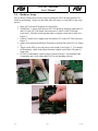
1. Place LPC3180 and GUI boards on a flat surface.
2. OPTIONAL: Connect GUI board to LPC3180 board by lining up connectors J12
and J13 of the LPC3180 board with connectors J1 and J2 of the GUI board,
respectively. Push the boards together until a complete connection is made (see
Figure 1).
3. Connect Condor Power supply from wall outlet to P3 on the LPC3180 board (see
Figure 3).
4. Setup serial connection and HyperTerminal as described in section 2.6 (see Figure
2).
5. Toggle switch SW1 to provide power to the board(s) (see Figure 3). Text should
be immediately visible in the HyperTerminal window and on the LCD panel (if
connected).
6. If JTAG is immediately required, please consult section 4.1 on installing JLink
Commander and 6.0 on connecting JTAG for downloading software.
Figure 1: GUI Board Connection
Figure 2: Serial Connection
Figure 3: Power Switch
Rev 2
Page 6
10/1/2007
FDI
4.0
NXP LPC3180 Demo
User’s Manual
FDI
Software Installation
4.1 Host PC
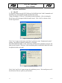
To download images into the LPC3180 board’s NAND flash, the J-Link Commander tool
should be used. To install this product, double-click on the
“Setup_JLinkARM_V356b.exe” file included in the distribution. After executing the
file, the user will be prompted with the install wizard. Click “Next” to advance to the
License Agreement:
Figure 4: JLink License Agreement
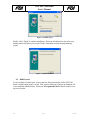
Click “Yes” to agree to the license and “Next” to advance to the “Destination Location”
window. The software should be installed in C:\Program
Files\SEGGER\JLinkARM_V356b. Batch files included in the distribution reference the
binary at this location. Therefore, if this installation path is modified the batch files must
be updated with the new path:
Figure 5: Destination Location
Click “Next” and “Next” again to begin the installation process. The install process will
be reflected as files are copied to your machine:
Rev 2
Page 7
10/1/2007
FDI
NXP LPC3180 Demo
User’s Manual
FDI
Figure 6: Install Progress
Finally, click “Finish” to end the installation. Shortcuts should now be placed on your
desktop which will allow you to open JLink Commander and run the programming
scripts.
Figure 7: Finish Installation
4.2 Build System
To successfully re-build kernel, u-boot, and root filesystem images for the LPC3180
board, a build system must be set up. This requires setting up a proper environment for
cross-compiling ARM binaries. Please see www.gnuarm.com for details on how to set
up such a system.
Rev 2
Page 8
10/1/2007
FDI
5.0
NXP LPC3180 Demo
User’s Manual
FDI
Boot Process
This section provides a detailed description of the boot process for the LPC3180 board.
First, a general list of steps is given as an overview to the boot process. A more detailed
explanation is then provided for the main applications responsible for loading Linux on
the LPC3180.
The boot process of the LPC3180 project is broken up into the following general steps:
1. On power-up, the LPC3180 begins booting by reading block 0 from the NAND
flash.
2. The secondary boot loader called SIBL is loaded from NAND flash, stored in the
LPC3180’s internal RAM, and executed.
3. SIBL performs initialization commands on the LPC3180 and loads the u-boot,
Linux Kernel, and root filesystem images from NAND flash into SDRAM at
predefined locations.
4. U-Boot is then executed which performs other checks and initialization steps and
finally executes the Linux Kernel image already in memory.
5. Linux boots using standard SysV Init and automatically modprobes all required
kernel modules.
6. The user may then log into the LPC3180 board as superuser “root” with no
password.
5.1 SIBL
The SIBL is the secondary boot loader that is executed before U-Boot. SIBL is
responsible for most of the required initialization and also provides a mechanism to run
functional tests on the LPC3180 board. A list of SIBL’s main responsibilities includes:
1.
2.
3.
4.
5.
Lock in the PLL to allow the LPC3180 to run at 208 MHz
Initialize, configure, and perform a quick read/write test on the SDRAM
Setup NAND controller and load the images out of Flash to SDRAM
Perform a CRC check on loaded images to verify their integrity
Walk through blocks in SDRAM until an executable image (U-Boot) is located
and run.
On startup, the three LEDs located just above the LPC3180 will blink indicating CPU
activity. Following this the LEDs will count from 1 to 5 in binary as SIBL progresses
through various stages. This is useful in circumstances when the GUI board is not
plugged in and a HyperTerminal connection is not being made from a Host PC.
The functional test mode may be entered by either holding down the F1 key on the
keypad of the GUI board or the space key on the keyboard of the Host PC running
HyperTerminal. For details on the purpose and use of the functional tests, please consult
section 9.0 Functional Test.
The SIBL must be programmed into NAND flash with a special tool that also sets the
first 512 bytes of the NAND flash to an appropriate configuration.
Rev 2
Page 9
10/1/2007
FDI
NXP LPC3180 Demo
User’s Manual
FDI
5.2 U-Boot
U-Boot is another boot loader which is mainly responsible for loading the Linux Kernel.
It also provides a number of useful utilities. For example, the auto-boot process can be
aborted and a command line system accessed to handle flashing of the NAND, memory
testing, and other basic low level features (read/write individual bytes). If left to run, UBoot will automatically start up the Linux system.
5.3 Linux Boot
Linux is loaded using a standard SysV Init method. As the kernel enters various runlevels scripts are executed which start specific daemons. One script run is the
/etc/rcS.d/S40modprobe.sh script. This file is actually a symbolic link to a script located
in /lib/modules/2.6.10/S40modprobe.sh. This script modprobes drivers on boot and may
be modified depending on the level of functionality desired in the bootable kernel.
After the kernel finishes booting, the login prompt is observable from the HyperTerminal
window. At this prompt, the user may log in by typing ‘root’ as the username with no
password:
Copacabana - ARM Embedded Linux version 1.1-vfp
Monday 20 December 2004 @ 20:40
(none) login:
5.4 SDRAM Memory Map
Although the images loaded into SDRAM depend on the parameters in the .ubt files,
below is the standard configuration used. The following depicts where the images are
loaded into memory, but the memory map may change as sections are uncompressed
and/or moved.
Section
Address Start
RootFS
0x80000000
Linux Kernel 0x80620000
U-Boot
0x81EC0000
5.5 NAND Flash Memory Map
The NAND Flash is split into the following sections:
Section
Interface Configuration data (ICR)
Secondary Boot Loader (SIBL)
RootFS
Linux Kernel
U-Boot
JFFS2 file system
Rev 2
Page 10
Address Start
0x00000000
0x00000800
0x00020000
0x00620000
0x00800000
0x01000000
10/1/2007
FDI
6.0
NXP LPC3180 Demo
User’s Manual
FDI
Downloading New Software
Please consult the FDI website, www.teamfdi.com/lpc3180 for updated board images
and other related software.
Updated software may be downloaded to the LPC3180’s NAND flash memory using a
two stage process. First, all images must be transferred via JTAG to the LPC3180’s
SDRAM. Next, these images in SDRAM are programmed into NAND flash using a
utility within U-Boot. This section outlines the steps necessary to accomplish these tasks.
6.1 Loading Images Into SDRAM Memory
If the images for download have not been provided, they will need to be built following
section 7.0
Rev 2
Page 11
10/1/2007
FDI
NXP LPC3180 Demo
User’s Manual
FDI
Building Images. Otherwise, the following steps may be used to transfer images to
SDRAM:
The serial connection to the LPC3180 board should be configured according to the steps
outlined in 2.6 Serial Connection.
To properly communicate with the board using J-Link Commander, the J-Link-ARM-KS
JTAG dongle should be connected to J2 on the LPC3180 Board (see Figure 8). J2 is
located between GUI board connectors J12 and J13 on the right-hand side of the
LPC3180 board. For assistance in installing J-Link Commander, please consult section
4.1.
Figure 8: LPC3180 JTAG Connection
After connecting the LPC3180 Board to the power supply (+5VDC, 2.5A, center +), use
the power switch SW1 to apply power on the board. If at any time the board needs to be
reset, push button SW3 may be pressed to reset the LPC3180 without toggling the power
switch.
Rev 2
Page 12
10/1/2007
FDI
NXP LPC3180 Demo
User’s Manual
FDI
Images may be downloaded to the LPC3180 Board’s SDRAM by double-clicking on the
“NXP Demo Setup” shortcut file or by entering the following commands manually into
the JLink Commander prompt window:
r
loadbin SIBL_208Mhz.bin, 0
setpc 0
g
h
s
s
s
s
speed 4000
// Switch the Thumb -> ARM
w2 0x0 0xa000
w2 0x2 0x4700
w4 0x4 0xeafffffe
setpc 0
g
h
loadbin u-boot.bin, 81EC0000
loadbin rootfs.ubt, 80020000
loadbin kernel.ubt, 80620000
loadbin uboot.ubt, 80800000
setpc 81EC0000
NOTE: The “NXP Demo Setup” shortcut ( ..\Software\Binaries\Programmed_Images)
expects JLink.exe to be located at "C:\Program
Files\SEGGER\JLinkARM_V356b\JLink.exe". If this is not the case on your system,
please modify the “NXP Demo Setup” shortcut.
NOTE: All .bin and .ubt files, except rootfs.ubt, should transfer to the LPC3180’s
SDRAM within a few minutes. The rootfs.ubt file may take up to 5 minutes to finish
downloading depending on its size.
To run u-boot for NAND flash programming, it is necessary to enter the following
commands into a J-Link Commander window. A new J-Link Commander window must
be opened if the above commands were not typed in manually.
setpc 81EC0000
g
After performing the above command, you will only have a few seconds to react and
enter U-Boot command prompt mode.
Rev 2
Page 13
10/1/2007
FDI
NXP LPC3180 Demo
User’s Manual
FDI
6.2 Writing SDRAM to NAND Flash
After the following u-boot banner appears, press any key to get to the command prompt.
Using default environment
In:
serial
Out:
serial
Err:
serial
Hit any key to stop autoboot:
2
After reaching the LPC3180 # prompt, the following commands should be executed
sequentially:
LPC3180
LPC3180
LPC3180
LPC3180
#
#
#
#
nand
nand
nand
nand
erase
write
write
write
00020000
80020000
80620000
80800000
00A00000
00020000 500000
00620000 160000
00800000 040000
The first command erases the entire portion of NAND memory to which the images will
be written. The second command writes the rootfs.ubt image to NAND and may take
several minutes to complete. The third command writes the kernel.ubt image to NAND
and the fourth command writes the uboot.ubt image to NAND.
If it is desirable to only erase a particular image, the following commands are useful:
LPC3180 # nand erase 00020000 500000
LPC3180 # nand erase 00620000 160000
LPC3180 # nand erase 00800000 040000
(filesystem)
(kernel)
(u-boot)
All commands listed here are also provided within the “nand prg commands.txt” file in
the distribution (..\Software\Programmed_Images).
Following the successful execution of the above commands, the board must be reset by
pressing SW3 or power cycling the board.
Rev 2
Page 14
10/1/2007
FDI
7.0
NXP LPC3180 Demo
User’s Manual
FDI
Building Images in Linux
The following section explains the direct steps needed to compile the UBT files from
their standard sources.
7.1 Building U-Boot
Currently, a patch should be applied against the standard u-boot-1.1.1 release. This
release can be downloaded from ftp://ftp.denx.de/pub/u-boot/u-boot-1.1.1.tar.bz2.
Next, the tarfile should be unzipped/extracted and the included patch applied to the
source:
tar jxvf u-boot-1.1.1.tar.bz2
cd u-boot-1.1.1
patch –p1 < ../path/to/u-boot-1.1.1-lpc3180_FDI.patch
To compile U-boot, enter these commands (requires gnu arm-tools installed in
/usr/local/arm/gnu):
export PATH=$PATH:/usr/local/arm/gnu/release-3.4.0-vfp/bin/armlinux-gcc
export ARCH=arm
export CROSS_COMPILE=arm-linuxmake distclean
make lpc3180db_config
make
make u-boot.axf
./tools/mkimage -A arm -O u-boot -T Firmware -C none -a 81EC0000 -e
81EC0000 –n “NXP Demo U-Boot v0.01” -d u-boot.bin uboot.ubt
7.2 Building the Linux Kernel
Currently, the patch provided should be applied against the vanilla linux-2.6.10 kernel.
Therefore, this tree should be downloaded from www.kernel.org. Next, the tarfile
should be unzipped/extracted and the included patch applied to the source:
tar zxvf linux-2.6.10.tar.gz
cd linux-2.6.10
patch –p1 < ../path/to/linux-2.6.10-lpc3180_FDI.patch
To compile the kernel, use the following commands (requires gnu arm-tools installed in
/usr/local/arm/gnu):
export PATH=$PATH:/usr/local/arm/gnu/release-3.4.0-vfp/bin/armlinux-gcc
export ARCH=arm
export CROSS_COMPILE=arm-linuxsource ./setup_links
make clean
make lpc3000evb_defconfig
make
make uImage
Rev 2
Page 15
10/1/2007
FDI
NXP LPC3180 Demo
User’s Manual
FDI
mkimage -A arm -O Linux -T Kernel -C none -a 80620000 -e 80620000 –n
“NXP Demo Linux-2.6.10” -d arch/arm/boot/uImage kernel.ubt
7.2.1. Kernel Modules
In the case where kernel modules must change, it is necessary to install the kernel
modules into the root file system image and re-download the image onto the board (see
section 6.0 Downloading New Software). This is performed by mounting the root file
system (see section 7.3 Editing the root file system) and performing the following
commands:
export INSTALL_MOD_PATH=/path/to/mnt_rootfs
make modules_install
This will install all newly compiled kernel modules into the directory
/path/to/mnt_rootfs/lib/modules/2.6.10.
Unfortunately, the ST Codec and WIFI kernel modules are over-written when this occurs.
The modules should be copied over into their respective locations:
cp vhw.ko /path/to/mnt_rootfs/lib/modules/2.6.10/kernel/drivers/i2c
cp ga_linuxdrv_211_pnx4008_spi.ko
/path/to/mnt_rootfs/lib/modules/2.6.10/kernel/drivers/net
Additionally, the file /path/to/mnt_rootfs/lib/modules/2.6.10/modules.dep must be
modified so that the “modprobe” command may be used to insert and remove the vhw.ko
driver. The following line should be added:
/lib/modules/2.6.10/kernel/drivers/i2c/vhw.ko:
This indicates to the module loader that the kernel module has no dependencies.
7.3 Editing the root file system
Before editing the file system, you must mount it. On a Linux build machine, enter
gzip –d ../Software/rootfs/root_fs.gz
mount –o loop root_fs ../path/to/mnt_rootfs/
Make changes to the files in mnt_rootfs and then enter these commands:
umount mnt_rootfs
gzip root_fs
mkimage -A arm -O Linux -T Filesystem -C none -a 80800000 -e 0 –n
“NXP Demo RootFS v0.00” -d root_fs.gz rootfs.ubt
Rev 2
Page 16
10/1/2007
FDI
8.0
NXP LPC3180 Demo
User’s Manual
FDI
Linux Features
8.1 USB Block Device
To connect a USB block device such as a USB Flash Drive to the LPC3180 board,
simply insert it into connector P2 on the lower-right of the board. As of Rev2, the board
now provides USB power to external devices. The following command should be issued
to force USB into host mode:
echo host > /sys/devices/platform/container-dev-1/forced_mode
The device may then be connected to the hub. Some messages should print to
hyperterminal following the insertion of the device informing the user a device has been
located. For the first device inserted, the first partition is found at /dev/sda1 whereas the
second device will be found at /dev/sdb, and so on. After the device settles, the following
commands may be used to create a mount point and mount the device:
mkdir /mnt/usb
mount –t auto /dev/sda1 /mnt/usb
NOTE: As of Release 1.03, the command above is already issued on boot and it is not
necessary to re-issue it within Linux. As a result, following boot a USB Block Device
may be inserted at any time.
8.2 JFFS2
In the on-board NAND Flash, a space of 15 Megs has been reserved for a JFFS2 image.
Follow these instructions to mount the drive:
mkdir /nv
mount -t jffs2 /dev/mtdblock0 /nv
NOTE: As of Release 1.03, the above commands are already issued on boot and it is not
necessary to re-issue them within Linux. Furthermore, a check is made on startup for the
existence of the file /nv/startup.sh. If this file exists, it is executed. This allows the user
to include custom startup utilities without reprogramming the board.
8.3 WIFI
Disclaimer: BGW211 drivers available on the reference design are available for
use. They are supported "as is" and there is no commitment from NXP or FDI for
bug fixing. An updated driver will likely be available in Q4-2007. Existing driver on
the system has been tested in the lab environment, but has not been certified by any
SIG. If a problem is found, refer to the "as is" statement above.
To enable WIFI on the LPC3180 board, special commands must be issued prior to the
loading of the module. The commands are:
echo "cs=1,client=wlan,cs_pin=GPO_21,flags=1,mbx_int=36,mbx_pin=
gpi_11" > /sys/devices/platform/spi-pnx1/cs_table
Rev 2
Page 17
10/1/2007
FDI
NXP LPC3180 Demo
User’s Manual
FDI
cat /sys/devices/platform/spi-pnx1/cs_table
The module itself can be found in the kernel module repository
(/lib/modules/2.6.10/kernel/drivers/net/ga_linuxdrv_211_pnx4008_spi.ko), but is not
loaded in the same manner as the other drivers due to the necessity of the two above
commands. To facilitate driver setup and configuration, a startup script called
“startWIFI.sh” is created and placed within the /nv directory on the LPC3180 board. By
default, each script is setup to statically assign the IP and MAC addresses of the board
according to the serial number on the board. For example, if the board’s serial number is
32, its IP address is 192.168.1.32 and the MAC address is aabbccd7ea32. Please note
that if the serial number is only 1 or 2 digits, the place-holder for the 100’s and 10’s digit
in the MAC address is replaced with the letter ‘a’. The ESSID, MODE, and WEP key are
left unmodified in the script to be configured by the user. Standard ‘wireless-tools’
commands are used to configure WIFI within the scripts.
8.4 Bluetooth
Each LPC3180 board is equipped with the NXP BGB203 Bluetooth module programmed
with version 1.2.4 of the NXP 1SPP firmware.
For correct operation, a modified version of the pshs_uart.ko kernel module must be used
which raises the reset line to the BGB203 upon initialization. Also, the pshs_uart.ko
module creates three high-speed UART devices according to the layout of the LPC3180.
The BGB203 is connected to UART2 which corresponds to /dev/ttyPSHS0 within the
device filesystem. Communication with the BGB203 is accomplished with modem
commands sent over the UART. Please consult the 1SPP user’s manual for more
information.
8.5 Framebuffer
The included GUI board comes equipped with an LCD panel controlled by the Solomon
Systech SSD1783U2 LCD Controller. For access within Linux, a framebuffer kernel
module was written and is included in the kernel patch file.
The following table shows a list of files and their purpose as they relate to the
framebuffer module. Each file is placed into the kernel tree after the linux-2.6.10lpc3180_FDI.patch file is applied.
Rev 2
File
ssdfb.c
Location
${LINUX}/drivers/video
ssdfb.h
${LINUX}/include/linux
Page 18
Description
The framebuffer driver code.
This code interacts with the linux
kernel to create and manipulate
the framebuffer device.
Contains IOCTL defines and
others used by ssdfb.c. Should
10/1/2007
FDI
NXP LPC3180 Demo
User’s Manual
FDI
be included by user applications
to access IOCTL commands.
LCD_SSD1783B.c
${LINUX}/drivers/video
This file contains the low-level
code to communicate with the
SSD1783U2 controller. It must
be linked with the ssdfb.c code
during module compilation.
LCD_SSD1783B.h
${LINUX}/include/linux
This file contains defines and
functional prototypes for all
capabilities of the SSD1783U2
controller.
LPC3180_GPIO.h
${LINUX}/include/linux
This file contains defines for
working with the LPC3180
GPIO pins.
Makefile
${LINUX}/drivers/video
This file has been modified to
include framebuffer support
directly into the linux kernel.
Also, lines were added to
successfully compile ssdfb.c and
link it during the ‘make
modules’ stage of compilation.
lpc3000evb_defconfig ${LINUX}/arch/arm/configs This file contains modifications
to enable framebuffer support
directly in the kernel when
building kernel images.
setup_links
${LINUX}
This file is sourced prior to
cross-compiling the linux kernel
for the ARM architecture. It
specifically sets the
CONFIG_FB_SOLSYS
environment variable to ‘m’ to
compile the ssdfb as a module.
During kernel compilation, it is important to set the following environment variable to
build the framebuffer module with the rest of the kernel:
export CONFIG_FB_SOLSYS=m
If desirable, this command can be placed within the setup_links file within the kernel
root.
Please consult section 14.0 APPENDIX C Framebuffer API for a detailed list of IOCTL
commands to interact with the framebuffer in a user-space application.
Rev 2
Page 19
10/1/2007
FDI
9.0
NXP LPC3180 Demo
User’s Manual
FDI
Functional Tests
A group of functional tests are bundled with SIBL for verification and debugging
purposes on the LPC3180 board. This section describes these functional tests and shows
how they are useful in trouble-shooting the board. A list of the functional tests is
provided below:
1.
2.
3.
4.
5.
LED Test
I2C Tests
SPI Tests
Uart2 to Bluetooth Test
Exhaustive Memory Test
9.1 Entering Functional Test Mode
To access the functional tests within SIBL, the F1 key should be pressed and held while
the power switch (SW1) is toggled. Alternatively if the GUI board is not present, the
space key may be tapped after observing the following text in HyperTerminal:
NXP LPC3180 Demo
FDI SIBL v1.00
SIBL will perform initialization and the quick memory test before going into Functional
Test Mode.
9.2 Functional Test Menu
Figure 9 shows the main menu listing all functional tests to choose from. The number
keys on the keyboard or GUI keypad may be used to make selections. The particular test
selected will be highlighted in white. For example, in Figure 9, functional test “2. Test
I2C1” is selected. After pressing the number of the test desired, the Enter key/OK button
should be pressed to enter the test.
Figure 9: Functional Tests Menu
Also, if using the GUI board, the up and down keys on either side of the ‘OK’ button may
be used to scroll through the tests.
Pressing the Esc key/End button will exit functional test mode and boot the LPC3180
board into Linux as normal.
Rev 2
Page 20
10/1/2007
FDI
NXP LPC3180 Demo
User’s Manual
FDI
9.3 Test LEDs
This test verifies functional GPIO pins from the LPC3180 as well as proper operation
from the LEDs themselves. After selecting the test, the user may repeatedly press the
space key/OK button to light up LED 1, LED 2, or LED 3. The LEDs should follow the
pattern 1, 2, 3, and then repeat. As the user continually presses the test will echo out the
LED number currently lit. Figure 10 shows the LCD and LEDs after pressing the OK
button a number of times.
Figure 10: LED Test
To end the test, the Enter key/Clear button may be pressed. This will bring up the main
menu.
9.4 Test I2C1
The I2C1 Test proceeds to probe a range of addresses for devices connected to the I2C1
bus. This test begins immediately when the user selects it from the main menu. If an
address times out, a message is printed to the screen and the word “FAILED” is printed
in red indicating the there was a problem with the test. If the test runs correctly, two
devices should be found at 0x10 and 0x48. Figure 11 shows a successful test run for
I2C1.
Figure 11: I2C1 Test
Rev 2
Page 21
10/1/2007
FDI
NXP LPC3180 Demo
User’s Manual
FDI
After the test runs, the user may press the Enter key/OK button to return to the main
menu.
9.5 Test I2C2
This test is exactly like the I2C1 test outlined in the previous section. However, devices
are probed for at a different location, and devices should be found at different locations.
For this test, devices should be located at 0x34 and 0xE2.
9.6 Test SPI
The SPI1 and SPI2 tests are currently wrapped up into a single SPI test from the main
menu. This test verifies correct operation of the SPI bus by sending out a pattern which
may be observed using an oscilloscope.
The oscilloscope should be configured with a trigger value of 1V and 1ms/Div. The
ground may be connected to pin 20 of JTAG connector J4 as shown in Figure 12.
Figure 12 Oscilloscope Ground Connection
After selecting the test, place the probe on the right side of resistor R145 and press the
Space key/OK button to issue the test. A spike should be observed on the oscilloscope
output indicating successful communication across the SPI1 bus. If the spike is not
observed, verify the probe is on the resistor properly, and press the Space key/OK button
again to re-issue the test. This process should be repeated for R144. The locations of
these resistors are shown in Figure 13.
Rev 2
Page 22
10/1/2007
FDI
NXP LPC3180 Demo
User’s Manual
FDI
Figure 13: Probe locations for SPI1 Test
Figure 14: Probe locations for SPI2 Test
After satisfactory results are obtained, the Enter key/Clear button may be pressed to
advance to the SPI2 test. During this test, the oscilloscope probe should be moved to pins
1 and 2 on connector J16 (see Figure 14), and the same procedure should be used to issue
the test.
To exit the test and return to the main menu, the Enter key/Clear button may be pressed.
9.7 Test UART2 to Bluetooth
This test verifies the connection of UART2 from the LPC3180 to the Bluetooth device.
After selecting the test from the main menu, the Space key/OK button may be used to
send the ‘U’ character over the UART. To verify this actually takes place, the
oscilloscope should be configured as described in the previous section. The oscilloscope
probe should be connected to pin 2 of U33 as shown in Figure 15. A similar spike as in
the previous test should be observable on the oscilloscope output when the ‘U’ is sent
across the UART.
Figure 15: Probe Connections for UART Test
Rev 2
Page 23
10/1/2007
FDI
NXP LPC3180 Demo
User’s Manual
FDI
9.8 Exhaustive Memory Test
The memory test within the functional test code is very different from the quick memory
check implemented in the SIBL POST code. This memory test will continually write a
different pattern to each location in SDRAM and read back the pattern to make sure the
write was successful. The sequence of the test goes as follows:
1.
2.
3.
4.
Write a pattern to each location in SDRAM
Read back the pattern from each location to make sure the write was successful.
Complement the pattern and repeats steps 1 and 2.
Increment the pattern and repeats steps 1 through 4.
Due to the nature of the test, it may be exited at any time by pressing and holding the
“Clear” key on the GUI keypad until the test returns to the main menu. Also, if using
HyperTerminal, the space key may be tapped and the test will return to the main menu
following its current iteration.
9.9 ST Codec Loopback test
The current ST Codec kernel module only provides minimal initialization commands for
the chip and currently cannot be used for any particular purpose without modification.
To verify chip activity a special version of this driver was created to affectively retransmit all sound received on a headset microphone to the headset speaker. By default,
this driver is not loaded, but a slight modification within the /nv/startup.sh file allows it to
be enabled on boot. Simply uncomment the following lines in the file to test the
loopback driver:
#############################################
### ST Codec Loopback
#############################################
# Uncomment the following lines to remove the ST Codec driver
# and insmod the loopback one
#/bin/lsmod | grep -q vhw
#if [ $? -eq 0 ]
#then
#
echo "Unloading vhw module..."
#
modprobe -r vhw
#fi
#echo "Loading loopback vhw module..."
#insmod /nv/STloopback/vhw.ko
NOTE: In some cases it was necessary to directly connect the digital and analog grounds
to successfully hear the loopback. This is accomplished by connecting pin 2 of J11 to pin
8 of J17.
Rev 2
Page 24
10/1/2007
FDI
NXP LPC3180 Demo
User’s Manual
FDI
10.0 Technical Support
NXP Semiconductors provides technical support for the LPC3180 and other NXP devices
utilized on this board. Please contact your local NXP sales office or Field Applications
Engineer.
IAR Systems provides technical support for the J-Link Commander Software and J-LinkARM-KS dongle. You may request assistance for any issues encountered by filling out a
request form at http://supp.iar.com/Support/Request/.
Technical support for the LPC3180 Development Kit is provided by Future Designs, Inc.
For fastest response;
• e-mail:
[email protected]
• fax:
(256) 883-1241
• phone:
(256) 883-1240.
FDI also provides a Web site at: http://www.teamfdi.com. This web site provides the
latest product information and updates for all FDI products.
11.0 General Sales and Contact Information
11.1 General Sales
Authorized sales representatives for the LPC3180 Development Kit include:
Worldwide contact:
FDI
http://www.teamfdi.com
(256) 883-1240
11.2 Contact Information
The following is a list of company contact information related to the NXP LPC3180 Kit.
NXP Semiconductors web site: http://www.nxp.com
IAR Systems web site at http://www.iar.com
Rev 2
Page 25
10/1/2007
FDI
NXP LPC3180 Demo
User’s Manual
FDI
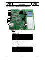
12.0 APPENDIX A: Board Layout and Connectors
J3
J5
J4
J6
J13
P3
J11
J2
J15
J16
J7
J1
J12
P1
Connection
J1
J2
J3
J4
J5
J6
J7
J9
J11
J12
J13
J15
J16
P1
P2
P3
P2
Usage
SDCard
JTAG (LPC3180)
50 Ohm Antenna (Bluetooth)
JTAG (Bluetooth)
50 Ohm Main Antenna (WLAN)
50 Ohm AUX Antenna (WLAN)
8 Ohm External Speaker Connection
BGW211 UART Header
Daughter Board Connector 1
GUI Keypad Connector
GUI Display Connector
Headset Jack (to Audio Codec - STw5095)
Daughter Board Connector 2
DB9 Serial (Female)
USB (Type-A, Female)
Power (5V, 2.4A, center positive)
Table 3: LPC3180 Connectors
Rev 2
Page 26
10/1/2007
FDI
NXP LPC3180 Demo
User’s Manual
FDI
13.0 APPENDIX B: Schematic and Parts List
Please refer to the Hardware documentation within the distribution for latest schematics
and parts list for the LPC3180 Demo Board.
14.0 APPENDIX C: Framebuffer API
14.1 IOCTL Calls
Applications in the userspace may manipulate the LCD controller using certain IOCTL
commands provided by the framebuffer module. This section outlines these IOCTL calls,
lists expected arguments, and provides an example of its use.
1. FBIO_DUMPSCREEN
a. Purpose: Updates the screen with the latest data written to memory. The
4 arguments allow the user to update a localized portion of the screen or
the whole screen if desired.
b. Arguments: Address of 4 element unsigned int array using the following
format: { x_Location, y_Location, x_Resolution, y_Resolution }
c. Returns: 1 on failure, 0 on success
d. Example:
unsigned int to_send[4]={0, 0, 128, 160};
if (ioctl(fbfd, FBIO_DUMPSCREEN, &to_send )) {
printf("Error dumping memory to LCD.\n");
exit(1);
}
2. FBIO_TOGGLEONOFF
a. Purpose: This command turns off the LCD Controller if it is on or turns it
on if the LCD Controller is off.
b. Arguments: None
c. Returns: 1 on failure, 0 on success
d. Example:
if (ioctl(fbfd, FBIO_TOGGLEONOFF)) {
printf("Error toggling screen on/off.\n");
exit(1);
}
3. FBIO_SCREENOFF
a. Purpose: Turns off the screen if it is on. If the screen is already off, this
command has no effect.
b. Arguments: None
c. Returns: 1 on failure, 0 on success
Rev 2
Page 27
10/1/2007
FDI
NXP LPC3180 Demo
User’s Manual
FDI
d. Example:
if (ioctl(fbfd, FBIO_SCREENOFF)) {
printf("Error turning screen off.\n");
exit(1);
}
4. FBIO_SCREENON
a. Purpose: Turns on the screen if it is off. If the screen is already on, this
command has no effect.
b. Arguments: None
c. Returns: 1 on failure, 0 on success
d. Example:
if (ioctl(fbfd, FBIO_SCREENON)) {
printf("Error turning screen on.\n");
exit(1);
}
5. FBIO_TOGGLESLEEP
a. Purpose: This command puts the LCD panel to sleep if it is awake or
wakes it if the LCD panel is asleep.
b. Arguments: None
c. Returns: 1 on failure, 0 on success
d. Example:
if (ioctl(fbfd, FBIO_TOGGLESLEEP)) {
printf("Error toggling screen sleep.\n");
exit(1);
}
6. FBIO_SLEEPON
a. Purpose: If the LCD panel is awake, this command explicitly puts it to
sleep. If the LCD panel is asleep, this command has no effect.
b. Arguments: None
c. Returns: 1 on failure, 0 on success
d. Example:
if (ioctl(fbfd, FBIO_SLEEPON)) {
printf("Error turning sleep on.\n");
exit(1);
}
7. FBIO_SLEEPOFF
a. Purpose: If the LCD panel is asleep, this command explicitly wakes it up.
If the LCD panel is awake, this command has no effect.
b. Arguments: None
c. Returns: 1 on failure, 0 on success
d. Example:
Rev 2
Page 28
10/1/2007
FDI
NXP LPC3180 Demo
User’s Manual
FDI
if (ioctl(fbfd, FBIO_SLEEPOFF)) {
printf("Error turning sleep off.\n");
exit(1);
}
8. FBIO_TOGGLEINVERT
a. Purpose: If the screen is not inverted, this command places the screen in
inverted mode. If the screen is inverted, this command places the screen
in normal mode:
b. Arguments: None
c. Returns: 1 on failure, 0 on success
d. Example:
if (ioctl(fbfd, FBIO_TOGGLEINVERT)) {
printf("Error toggling screen invert.\n");
exit(1);
}
9. FBIO_INVERTON
a. Purpose: If the screen is in normal mode, this command places the screen
in inverted mode. If the screen is already inverted, this command has no
effect.
b. Arguments: None
c. Returns: 1 on failure, 0 on success
d. Example:
if (ioctl(fbfd, FBIO_INVERTON)) {
printf("Error inverting screen.\n");
exit(1);
}
10. FBIO_INVERTOFF
a. Purpose: If the screen is in inverted mode, this command places the
screen in normal mode. If the screen is already in normal mode, this
command has no effect.
b. Arguments: None
c. Returns: 1 on failure, 0 on success
d. Example:
if (ioctl(fbfd, FBIO_INVERTOFF)) {
printf("Error inverting screen.\n");
exit(1);
}
11. FBIO_CONTRASTPLUS
a. Purpose: Increments the screen’s contrast adjustment by 1. If the contrast
adjustment is at its highest possible value, this command has no effect.
b. Arguments: None
c. Returns: 1 on failure, 0 on success
d. Example:
Rev 2
Page 29
10/1/2007
FDI
NXP LPC3180 Demo
User’s Manual
FDI
if (ioctl(fbfd, FBIO_CONTRASTPLUS)) {
printf("Error increasing screen contrast.\n");
exit(1);
}
12. FBIO_CONTRASTMINUS
a. Purpose: Decrements the screen’s contrast adjustment by 1. If the
contrast adjustment is at its lowest possible value, this command has no
effect.
b. Arguments: None
c. Returns: 1 on failure, 0 on success
d. Example:
if (ioctl(fbfd, FBIO_CONTRASTMINUS)) {
printf("Error decreasing screen contrast.\n");
exit(1);
}
13. FBIO_BRIGHTNESSPLUS
a. Purpose: Increments the screen’s brightness adjustment by 1. If the
brightness adjustment is at its highest possible value, this command has no
effect.
b. Arguments: None
c. Returns: 1 on failure, 0 on success
d. Example:
if (ioctl(fbfd, FBIO_BRIGHTNESSPLUS)) {
printf("Error increasing screen brightness.\n");
exit(1);
}
14. FBIO_BRIGHTNESSMINUS
a. Purpose: Decrements the screen’s brightness adjustment by 1. If the
brightness adjustment is at its lowest possible value, this command has no
effect.
b. Arguments: None
c. Returns: 1 on failure, 0 on success
d. Example:
if (ioctl(fbfd, FBIO_BRIGHTNESSMINUS)) {
printf("Error decreasing screen brightness.\n");
exit(1);
}
NOTE: In addition to the IOCTL commands above, the IOCTL calls
FBIOGET_FSCREENINFO and FBIOGET_VSCREENINFO are also available through
the generic Linux framebuffer interface.
Rev 2
Page 30
10/1/2007
FDI
NXP LPC3180 Demo
User’s Manual
FDI
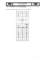
15.0 APPENDIX D: GUI Keypad Mapping
Each button is assigned a column (Cx) and row (Ry) as shown below.
Rev 2
Page 31
10/1/2007
FDI
Rev 2
NXP LPC3180 Demo
User’s Manual
Page 32
FDI
10/1/2007