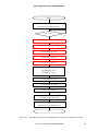
1
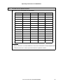
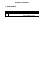
Customer Notification
V850E2/Px4
32-Bit Single-Chip Microcontrollers
Operating Precautions
µPD70F3506
µPD70F3507M1, µPD70F3507M2
µPD70F3508
µPD70F3509M1, µPD70F3509M2
www.renesas.com
R01TU0014ED0300, Ver. 3.00
December 19th, 2012
Operating Precautions for V850E2/Px4
Notice
1.
All information included in this document is current as of the date this document is issued. Such information, however, is
subject to change without any prior notice. Before purchasing or using any Renesas Electronics products listed herein,
please confirm the latest product information with a Renesas Electronics sales office. Also, please pay regular and careful
attention to additional and different information to be disclosed by Renesas Electronics such as that disclosed through our
website.
2.
Renesas Electronics does not assume any liability for infringement of patents, copyrights, or other intellectual property
rights of third parties by or arising from the use of Renesas Electronics products or technical information described in this
document. No license, express, implied or otherwise, is granted hereby under any patents, copyrights or other intellectual
property rights of Renesas Electronics or others.
3.
You should not alter, modify, copy, or otherwise misappropriate any Renesas Electronics product, whether in whole or in
part.
4.
Descriptions of circuits, software and other related information in this document are provided only to illustrate the operation
of semiconductor products and application examples. You are fully responsible for the incorporation of these circuits,
software, and information in the design of your equipment. Renesas Electronics assumes no responsibility for any losses
incurred by you or third parties arising from the use of these circuits, software, or information.
5.
When exporting the products or technology described in this document, you should comply with the applicable export
control laws and regulations and follow the procedures required by such laws and regulations. You should not use
Renesas Electronics products or the technology described in this document for any purpose relating to military applications
or use by the military, including but not limited to the development of weapons of mass destruction. Renesas Electronics
products and technology may not be used for or incorporated into any products or systems whose manufacture, use, or
sale is prohibited under any applicable domestic or foreign laws or regulations.
6.
Renesas Electronics has used reasonable care in preparing the information included in this document, but Renesas
Electronics does not warrant that such information is error free. Renesas Electronics assumes no liability whatsoever for
any damages incurred by you resulting from errors in or omissions from the information included herein.
7.
Renesas Electronics products are classified according to the following three quality grades: "Standard", "High Quality",
and "Specific". The recommended applications for each Renesas Electronics product depends on the product's quality
grade, as indicated below. You must check the quality grade of each Renesas Electronics product before using it in a
particular application. You may not use any Renesas Electronics product for any application categorized as "Specific"
without the prior written consent of Renesas Electronics. Further, you may not use any Renesas Electronics product for
any application for which it is not intended without the prior written consent of Renesas Electronics. Renesas Electronics
shall not be in any way liable for any damages or losses incurred by you or third parties arising from the use of any
Renesas Electronics product for an application categorized as "Specific" or for which the product is not intended where you
have failed to obtain the prior written consent of Renesas Electronics. The quality grade of each Renesas Electronics
product is "Standard" unless otherwise expressly specified in a Renesas Electronics data sheets or data books, etc.
Standard":
Computers; office equipment; communications equipment; test and measurement equipment; audio and
visual equipment; home electronic appliances; machine tools; personal electronic equipment; and industrial
robots.
"High Quality": Transportation equipment (automobiles, trains, ships, etc.); traffic control systems; anti-disaster systems;
anti-crime systems; safety equipment; and medical equipment not specifically designed for life support.
"Specific":
Aircraft; aerospace equipment; submersible repeaters; nuclear reactor control systems; medical equipment
or systems for life support (e.g. artificial life support devices or systems), surgical implantations, or
healthcare intervention (e.g. excision, etc.), and any other applications or purposes that pose a direct threat
to human life.
8.
You should use the Renesas Electronics products described in this document within the range specified by Renesas
Electronics, especially with respect to the maximum rating, operating supply voltage range, movement power voltage
range, heat radiation characteristics, installation and other product characteristics. Renesas Electronics shall have no
liability for malfunctions or damages arising out of the use of Renesas Electronics products beyond such specified ranges.
9.
Although Renesas Electronics endeavors to improve the quality and reliability of its products, semiconductor products have
specific characteristics such as the occurrence of failure at a certain rate and malfunctions under certain use conditions.
Further, Renesas Electronics products are not subject to radiation resistance design. Please be sure to implement safety
measures to guard them against the possibility of physical injury, and injury or damage caused by fire in the event of the
failure of a Renesas Electronics product, such as safety design for hardware and software including but not limited to
redundancy, fire control and malfunction prevention, appropriate treatment for aging degradation or any other appropriate
measures. Because the evaluation of microcomputer software alone is very difficult, please evaluate the safety of the final
products or system manufactured by you.
10.
Please contact a Renesas Electronics sales office for details as to environmental matters such as the environmental
compatibility of each Renesas Electronics product. Please use Renesas Electronics products in compliance with all
applicable laws and regulations that regulate the inclusion or use of controlled substances, including without limitation, the
EU RoHS Directive. Renesas Electronics assumes no liability for damages or losses occurring as a result of your
noncompliance with applicable laws and regulations.
11.
This document may not be reproduced or duplicated, in any form, in whole or in part, without prior written consent of
Renesas Electronics.
12.
Please contact a Renesas Electronics sales office if you have any questions regarding the information contained in this
document or Renesas Electronics products, or if you have any other inquiries.
(Note 1) “Renesas Electronics” as used in this document means Renesas Electronics Corporation and also includes its majorityowned subsidiaries.
(Note 2) “Renesas Electronics product(s)” means any product developed or manufactured by or for Renesas Electronics.
Customer Notification R01TU0014ED0300
2
Operating Precautions for V850E2/Px4
(A)
Table of Operating Precautions . . . . . . . . . . . . . . . . . . . . . . . . . . . . . . . . . . . . 4
(B)
Description of Operating Precautions. . . . . . . . . . . . . . . . . . . . . . . . . . . . . . . 5
No. 1
No. 2
No. 3
No. 4
No. 5
No. 6
No. 7
No. 8
No. 9
No. 10
No. 11
NEXUS interface specification is changed . . . . . . . . . . . . . . . . .5
The LVI registers are initialized after LVI reset . . . . . . . . . . . . .5
PC break set to a specific instruction . . . . . . . . . . . . . . . . . . . . .5
Unaligned data access crossing the upper boundary of MPU region DPA5 . . . . . . . . . . . . . . . . . . . . . . . . . . . . . . . . . . . . . . . . .7
Error Counter Clearing of FCN/DCN CAN controllers . . . . . . . .8
Unintended load causing RAM ECC error generation . . . . . . .15
Stop of AD conversion in repeat mode after start-trigger . . . . .16
Reset signal occurence and reset mask setting in debug mode .
16
Software reset during data flash control sequence execution .17
Consecutive write/read access against same address in uninitialized local RAM area . . . . . . . . . . . . . . . . . . . . . . . . . . . . . . . . .17
Data Flash Tag (Direction of Use) . . . . . . . . . . . . . . . . . . . . . .18
(C)
Related Documents. . . . . . . . . . . . . . . . . . . . . . . . . . . . . . . . . . . . . . . . . . . . . 19
(D)
Revision History . . . . . . . . . . . . . . . . . . . . . . . . . . . . . . . . . . . . . . . . . . . . . . . 20
Customer Notification R01TU0014ED0300
3
(A)
Table of Operating Precautions
No.
Outline
µPD70
F3506
µPD70F3507
M1
µPD70F
3508
M2
µPD70F3509
M1
M2
Ranka
1
NEXUS interface specification is changed
appl.
appl.
appl.
appl.
appl.
appl.
2
The LVI registers are initialized after LVI reset
appl.
appl.
appl.
not appl.
not appl.
not appl.
3
PC break set to a specific
instruction
appl.
appl.
appl.
not appl.
not appl.
not appl.
4
Unaligned data access
the
upper
crossing
boundary of MPU region
DPA5
appl.
appl.
appl.
not appl.
not appl.
not appl.
Error Counter Clearing of
FCN/DCN CAN controllers
(Direction of use)
appl.
appl.
appl.
appl.
appl.
appl.
Unintended load causing
RAM ECC error generation
appl.
appl.
appl.
appl.
appl.
appl.
Stop of AD conversion in
repeat mode after starttrigger
appl.
appl.
appl.
appl.
appl.
appl.
Reset signal occurence
and reset mask setting in
debug mode
appl.
appl.
appl.
appl.
appl.
appl.
Software reset during
flash
control
data
sequence execution
appl.
appl.
appl.
appl.
appl.
appl.
Consecutive
write/read
access against same
address in uninitialized
local RAM area
appl.
appl.
appl.
appl.
appl.
appl.
Data Flash Tag (Direction of Use)
appl.
appl.
appl.
appl.
appl.
appl.
5
6
7
8
9
10
11
a.
The rank is indicated by the letter appearing at the 5th position from the left in the lot number, marked on each
product.
not appl. :Not applicable
appl.:Applicable
Customer Notification R01TU0014ED0300
4
Operating Precautions for V850E2/Px4
(B)
No. 1
Description of Operating Precautions
NEXUS interface specification is changed
Details
The NEXUS interface DCUTCK frequency for MiniCube (QB-V850-EE) is specified to
20MHz.
Workaround
There is no workaround available.
No. 2
The LVI registers are initialized after LVI reset
Details
The LVI registers are set back to the reset values by the LVI reset when BIST is enabled.
Workaround
Set the LVI registers to the needed values after a reset.
No. 3
PC break set to a specific instruction
Details
If a PC break has been set to a specific instruction, the behaviour of the microcontroller is
wrong. The concerned instructions and microcontroller’s behaviour on PC break are:
1. HALT instruction:
•
CPU will complete the operation of instruction,
•
Debugger UI may hang-up,
•
After release of the HALT state (if possible), PC-break will be generated and branches to
Debug-Exception handler address.
2. Multiply instructions: MUL, MULH, MULHI, MULU, MAC, MACU:
•
Destination register of the instruction is updated.
3. FPU instructions (see table “Alphabetical list of concerned FPU instructions”:
•
Destination register might be updated
•
Floating-point system register might be updated
•
Floating-point exception might be generated
•
PC break is generated and branches to Debug-Exception handler address
Customer Notification R01TU0014ED0300
5
Operating Precautions for V850E2/Px4
No. 3
PC break set to a specific instruction
Alphabetical list of concerned FPU instructions:
Mnemonics
Mnemonics
Mnemonics
Mnemonics
Mnemonics
ABSF.D
CMOVF.S
CVTF.SUW
FLOORF.SUW
TRNCF.DUW
ABSF.S
CMPF.D
CVTF.SW
FLOORF.SW
TRNCF.DW
ADDF.D
CMPF.S
CVTF.ULD
MAXF.D
TRNCF.SL
ADDF.S
CVTF.DL
CVTF.ULS
MAXF.S
TRNCF.SUL
CEILF.DL
CVTF.DS
CVTF.UWD
MINF.D
TRNCF.SUW
CEILF.DUL
CVTF.DUL
CVTF.UWS
MINF.S
TRNCF.SW
CEILF.DUW
CVTF.DUW
CVTF.WD
MULF.S
CEILF.DW
CVTF.DW
CVTF.WS
NEGF.D
CEILF.SL
CVTF.LD
FLOORF.DL
NEGF.S
CEILF.SUL
CVTF.LS
FLOORF.DUL
SUBF.D
CEILF.SUW
CVTF.SD
FLOORF.DUW
SUBF.S
CEILF.SW
CVTF.SL
FLOORF.SL
TRNCF.DL
CMOVF.D
CVTF.SUL
FLOORF.SUL
TRNCF.DUL
Workaround
•
Renesas tool users: use latest EXEC file, where the workaround is already implemented.
•
Third-party tool users: contact your tool vendor for respective solution.
Customer Notification R01TU0014ED0300
6
Operating Precautions for V850E2/Px4
No. 4
Unaligned data access crossing the upper boundary of MPU region DPA5
Details
An unaligned data access crossing the configured upper boundary of the protection region
DPA5 will not be detected as an access violation.
For the DPA5 protection region the DPA5U register always specifies a “mask value” and the
DPA5L register is used to specify a “base address”. These registers set the needed address
range and therefore also the location of the upper boundary of this range.
If the address of an accessed data is located below the configured upper-boundary address
of DPA5 and due to the length of the data, the access will cause crossing of the upper
boundary - according to the present limitation an access violation will not be generated
although upper bytes of the unaligned access are located beyond/above the configured
upper boundary of DPA5 and an exception is expected.
Therefore it is recommended to avoid any unaligned accesses, which could lead to crossing
of the upper boundary of the DPA5 region.
Please refer to V850E2M Architecture User’s Manual (U19949EJ1V0UM00) for the DPA5U
and DPA5L registers description.
Workaround
There is no workaround available.
Customer Notification R01TU0014ED0300
7
Operating Precautions for V850E2/Px4
No. 5
Error Counter Clearing of FCN/DCN CAN controllers
Details
For the Px4 devices, the FCN applies.
In applications, which are clearing the error counter status during run-time, use one of
the following procedure recommendations:
Notes:
1. The error counters referred to in this document are located in the registers
FCNnCMINSTR, FCNnCMERCNT, DCNnCMINSTR, DCNnCMERCNT and
DCNnCRERCNT.
2. The Clear Error Counter flags referred to in this document are located in the
FCNnCMCLERCF/DCNnCMCLERCF/DCNnCRCLERCF bits
(1) Shutdown of CAN Module after reaching Initialization Mode
If FCN or DCN is shut down and re-started, after the initialization mode has been
reached, all error counter states are cleared anyway. In addition, this also serves as a
procedure to avoid any unexpected behaviour situation.
Follow the sequence below in strict order from (a) to (c).
(a) Set the FCNnGMCLCLOM / DCNnGMCLCLOM flag to clear the
FCNnGMCLPWOM / DCNnGMCLPWOM global operation mode bit.
Caution:
Confirm the clearance by reading back. If unsuccessful, use the
forced shutdown by setting the FCNnGMCLESDE / DCNnGMCLESDE
in advance.
(b)Re-start the CAN controller by setting the FCNnGMCLSEOM /
DCNnGMCLSEOM bit.
Note: This leads back to initialization mode, with all error counter states cleared.
(c) Restore the register settings of the CAN module configuration.
The following register settings must be restored, because they are reset to their initial
values, when the CAN module was shut down.
• FCNnGMADCTL / DCNnGMADCTL
• FCNnCMMKCTLx / DCNnCMMKCTLx
• FCNnCMCLCTL / DCNnCMCLCTL / DCNnCRCLCTL
• FCNnCMIECTL / DCNnCMIECTL / DCNnCRIECTL
• FCNnCMBRPRS / DCNnCMBRPRS / DCNnCRBRPRS
• FCNnCMBTCTL / DCNnCMBTCTL / DCNnCRBTCTL
• FCNnCMTSCTL / DCNnCMTSCTL / DCNnCRTSCTL
• DCNnCRBSSTR
• DCNnTIDRTXxH/yW
• DCNnTIDMTX0H/1H
Registers of all message buffers
Notes:
1. The interrupt status flags of FCNnCMISCTL / DCNnCMISCTL / DCNnCRISCTL
are cleared and cannot be restored.
Customer Notification R01TU0014ED0300
8
Operating Precautions for V850E2/Px4
No. 5
Error Counter Clearing of FCN/DCN CAN controllers
2. The contents of the history lists are cleared and cannot be restored.
3. All message buffer contents need not to be restored, even though following flags
must be cleared.
•
FCNnMmCTL.FCNnMmDTNF / DCNnMmCTL.DCNnMmDTNF
•
FCNnMmCTL.FCNnMmTRQF / DCNnMmCTL.DCNnMmTRQF
Please refer also to Figure 2-1 “Shutdown and restart of CAN Module to clear Error
Counters of FCN” on page 11 and Figure 2-2 “Shutdown and restart of CAN Module
to clear Error Counters of DCN” on page 12 .
(2) Clearing of all Pending Transmit Requests
Follow the sequence below in strict oder from (a) to (d).
Before entering the initialization mode of either FCN or DCN, always:
(a) Set the RXONLY_CH of the DCN to initialization mode and confirm this by
reading DCNnCRCLMDOF[2:0] == 0.
Note: This is only required for DCN, if the RXONLY_CH was operated in the mirror
mode.
(b)Clear any pending ABT mode trigger.
Caution:
Confirm the clearance and stopping of the ABT operation by reading
the FCNnGMABCTL.FCNnGMABABTT /
DCNnGMABCTL.DCNnGMABABTT flag.
(c) Clear all transmit requests by software.
Cautions:
1. Any flag “FCNnMmTRQF” or “DCNnMmTRQF” must be cleared.
2. Clearing of “FCNnMmTRQF” or “DCNnMmTRQF” must be confirmed by reading
back.
3. Do this also for all message buffers of the upper mirror area of DCN.
(d)Wait on transmission completion by 11 CAN bits and cleared Transmission
Status Flag.
Caution:
Confirm the transmission completion by waiting for 11 CAN bits and
check that the transmission status flag FCNnCMCLSSTS is not set
after that. This is according to a recommended transmission abort
processing flow.
Please refer also to Figure 2-3 “Clearing of Transmit Requests for FCN before clearing
Error Counters” on page 13 and Figure 2-4 “Clearing of Transmit Requests for DCN
before clearing Error Counters” on page 14 .
(3) Do not clear error counters except after “bus off”
In “bus off” state, the operating precaution is not applicable. Therefore, there is no
restriction in usage of the FCNnCMCLERCF / DCNnCMCLERCF, when the CAN controller is in “bus off” state.
Note: The “bus off” state can be determined by reading the FCNnCMINBOFF /
DCNnCMINBOFF bit.
Customer Notification R01TU0014ED0300
9
Operating Precautions for V850E2/Px4
No. 5
Error Counter Clearing of FCN/DCN CAN controllers
(4) Do not clear the error counter states at all
According to ISO, this approach is recommended.
Like this, a node will behave according to the ISO 11898 specification. The behaviour
of a node during “bus off” and the behaviour of restoring of the “error passive” state of
a node are the impacts of this procedure. If the error counters are not cleared, the penalties of the ISO specification for erroneous nodes will become active, which are typically resulting in degraded performance on the CAN bus, until the node has recovered
to “error active” state.
Workaround
Use one of the following procedure recommendations.
Customer Notification R01TU0014ED0300
10
Operating Precautions for V850E2/Px4
START
Clear
FCNnCMCLCTL.FCNnCMCLMDOF[2:0]
INIT mode?
Yes
No
Clear FCNnGMCLCTL.FCNn GMCLPWOM
Set FCNnGMCLCTL.FCNnGMCLPWOM
Set FCNnGMADCTL register
Set FCNnCMTSCTL register
Set FCNnCMCLCTL register
Set
FCNnCMBRPRS register
FCNnCMBTCTL register
Set FCNnCMIECTL register
Set FCNnCMMKCTLx register
Initialize message buffers
Set
FCNnCMCLCTL.FCNnCMCLERCF
Set
FCNnCMCLCTL.FCNnCMCLMDOF[2:0]
END
Figure 2-1
Shutdown and restart of CAN Module to clear Error Counters of FCN
Customer Notification R01TU0014ED0300
11
Operating Precautions for V850E2/Px4
START
Clear
DCNnCRCLCTL.DCNnCRCLMDOF[2:0]
INIT mode?
No
Yes
Clear
DCNnCMCLCTL DCNnCMCLMDOF[2:0]
INIT mode?
No
Yes
Clear DCNnGMCLCTL.DCNnGMCLPWOM
Set DCNnGMCLCTL.DCNnGMCLPWOM
Set DCNnGMADCTL register
Set
DCNnCMBRPRS / DCNnCRBRPRS register
Set DCNnCMTSCTL / DCNnCRTSCTL register
DCNnCMBTCTL / DCNnCRBTCTL register
Set DCNnCRBSS TR register
Set DCNnCMIECTL / DCNnCRIECTL register
Set DCNnTIDRTXxH/yW register
Set DCNnCMMKCTLx register
Set DCNnTIDMTX0H/1H register
Initialize message buffers
Set DCNnCMCLCTL register
Set
DCNnCMCLCTL.DCNnCMCLERCF
Set
DCNnCMCLCTL.DCNnCMCLMDOF[2:0]
Set
DCNnCRCLCTL.DCNnCRCLMDOF[2:0]
END
Figure 2-2
Shutdown and restart of CAN Module to clear Error Counters of DCN
Customer Notification R01TU0014ED0300
12
Operating Precautions for V850E2/Px4
START
Clear
FCNnGMABCTL.FCNnGMABABTT
FCNnGMABCTL.FCNnGMABABTT
No
= 0?
Yes
Clear All
FCNnMmCTL.FCNnMmTRQF
Wait for 11 CAN data bits
No
FCNnCMCLCTL.FCNnCMCLSSTS
= 0?
Yes
Clear
FCNnCMCLCTL.FCNnCMCLMDOF[2:0]
INIT mode?
No
Yes
Set
FCNnCMBRPRS register
FCNnCMBTCTL register
Set FCNnCMIECTL register
Set FCNnCMMKCTL register
Initialize message buffers
Set
FCNnCMCLCTL.FCNnCMCLERCF
Set
FCNnCMCLCTL.FCNnCMCLMDOF[2:0]
END
Figure 2-3
Clearing of Transmit Requests for FCN before clearing Error Counters
Customer Notification R01TU0014ED0300
13
Operating Precautions for V850E2/Px4
START
Clear
DCNnCRCLCTL.DCNnCRCLMDOF[2:0]
No
INIT mode?
Yes
Clear
DCNnGMABCTL.DCNnGMABABTT
DCNnGMABCTL.DCNnGMABABTT
No
= 0?
Yes
Clear All
DCNnMmCTL.DCNnMmTRQF
Wait for 11 CAN data bits
DCNnCMCLCTL.DCNnCMCLSSTS
No
= 0?
Yes
Clear
DCNnCMCLCTL.DCNnCMCLMDOF[2:0]
No
INIT mode?
Yes
Set
DCNnCMBRPRS register
DCNnCMBTCTL register
Set DCNnCMIECTL register
Set DCNnCMMKCTL regist er
Initialize message buffers
Set
DCNnCMCLCTL.DCNnCMCLER CF
Set
DCNnCMCLCTL.DCNnCMCLMDOF[2:0]
Set
DCNnCRCLCTL.DCNnCRCLMDOF[2:0]
END
Figure 2-4
Clearing of Transmit Requests for DCN before clearing Error Counters
Customer Notification R01TU0014ED0300
14
Operating Precautions for V850E2/Px4
No. 6
Unintended load causing RAM ECC error generation
Details
An unintended load from undefined memory causes a RAM ECC error, and as a result
the INTECCLRED interrupt and the SEG_FLAG.RAMF bit is set, under following conditions:
1. An instruction (no. 1), which performs the unintended read access to undefined
memory, can be executed in parallel with another instruction,
2. An instruction (no. 2) before instruction no. 1 can be executed in parallel with
another instruction and must perform branch/jump where the execution of
instruction no. 1 is discarded ( -> unintended read access).
Under these conditions an instructions combination as below may result in the unintended read access:
•
Bcond, JARL, JMP or JR instruction followed by a
•
LD or SLD instruction.
Instructions combinations listed below do not result in the unintended read access:
1. Any other combination of instructions do not result in the unintended read access.
– Bit manipulation instructions or special instructions are not concerned, since
these will not be executed in parallel,
– e.g. data manipulation instructions are not concerned since these do not access
any memory.
2. When the first instruction is a JARL, JMP, JR of 6 bytes length, which uses a 32-bit
displacement, since these instructions will not be executed in parallel:
JARL disp32, reg1
JMP disp32 [reg1]
JR disp32
3. When the LD instruction has a length of 6 bytes, which uses a 23-bit displacement,
since this instruction will not be executed in parallel:
LD.W disp23 [reg1], reg3
Workaround
One of the following workarounds can be applied.
•
Avoidance of uninitialized pointers
The unintended load from undefined memory can be avoided generally when no
uninitialized pointers are used. Therefore it is recommended to initialize any
pointer in a C program to an existing address, or to the NULL pointer, respectively.
Customer Notification R01TU0014ED0300
15
Operating Precautions for V850E2/Px4
No. 6
Unintended load causing RAM ECC error generation
(cont.)
•
Treatment of ECC error by interrupt handler
The memory address where the ECC error occurred can be obtained using
LEDADR reister. Please add following software routine to the INTECCLRED
interrupt handler:
1. read LEDADR register,
2. add offset of FEC00000H to the read value to obtain the address where error
occurred,
3. if the resulting address value points to:
– defined internal RAM. In this case the ECC error occurred at the obtained
address and an error management actions have to be done,
– undefined memory area. In this case the software routine can skip to step 4,
4. clear respective error flags in the LECCER and SGAmESSTR0 registers.
Note: If the SEG_CONT.RAME bit is enabled, consider that a SYSERR exception
cannot be resumed.
No. 7
Stop of AD conversion in repeat mode after start-trigger
Details
In case a start-trigger occures during conversion end state (one ADCATCLK cycle
before conversion completion) of the last channel of the last repetition in a CG repeat
mode (ADCnSTM=0) the next repetitions of the conversion will be stopped.
Workaround
There is no workaround available.
No. 8
Reset signal occurence and reset mask setting in debug mode
Details
In debug mode, when an internal resset occurs and reset mask is set in the same time,
the reaction on the reset signal cannot be guaranteed.
Workaround
There is no workaround available.
Customer Notification R01TU0014ED0300
16
Operating Precautions for V850E2/Px4
No. 9
Software reset during data flash control sequence execution
Details
When a software reset occurs during data flash control sequence execution, only flash
related registers are initialized. This causes a difference between data flash library status (FDL) and status of data flash macro. Due to that the FDL will keep waiting on a
state of the data flash until a hardware reset or Safety Guardian reset is done.
Data flash control sequence execution means a state between start of FAL_Execute
function (request of Erase, Write, Write-Tag, Bit error check) and function end (return
value of FAL_HAndler function is FAL_BUSY).
Workaround
If the software reset has to be done in spite of executing the data flash access, please
execute a forced termination of data flash control sequence execution by FAL_Init
function before issuing the software reset.
No. 10
Consecutive write/read access against same address in uninitialized local RAM area
Details
In the write path to local RAM area there is a write buffer implemented. Due to this fact
and the fact, that read operation has higher priority than write operation, when a write
operation to an uninitialized local RAM address is directly followed by a read operation
from the same address, this read operation will result in a value read from the write
data buffer, but the data under the accessed RAM address will not be changed.
If the accessed RAM address has been already initialized, the result of consecutive
write/read operation will be correct. The read value and the real value under the
accessed RAM address will both be correct.
Workaround
Do not execute consecutive write and read operations to the same address in the
uninitialized local RAM area.
Customer Notification R01TU0014ED0300
17
Operating Precautions for V850E2/Px4
No. 11
Data Flash Tag (Direction of Use)
Details
The Data Flash of devices in UX6LF Flash technology is based on a standard 32-bit
architecture. This means, that the data can be written and read in 32-bit units (read or
write in 8-bit or 16-bit units is not possible). Additionally to every 32-bit data word a
33rd bit (Tag) is available for free usage.
While the 32 data bits can be read in a linear address room, the Tag can be read in
another linear address room on a different address (every 32-bit address one tag can
be read). The data address area starts from 0x02000000 while the Tag address area
starts from 0x02100000.
Furthermore, the Tag can be written independently from the other data and it is protected against bit failures separately. The FDL provides separate functions to write the
data and the tags.
Usage
The Tags are completely under control of the user application. In the EEPROM emulation library (EEL) concept, the Tag is used to write additional management data in
order to ensure data consistency in case of write interruptions.
Therefore, when the EEL is applied and the MPU is adopted to protect the memory
areas, the data flash tag area from 0x0210000 to 0x0217FFF has to be considered as
read/write access area.
Customer Notification R01TU0014ED0300
18
Operating Precautions for V850E2/Px4
(C)
Related Documents
These Operating Precautions are complementary to the following documents:
Item
Date published
Document No.
Document Title
1
July 2012
R01UH0098EJ0100
Px4 User’s Manual
2
December 2009
U19949EJ1V0UM00
V850E2M Preliminary Architecture User’s Manual
3
July 2010
U20280EE1V1UM00
V850 Single Voltage Flash devices with Data Flash
and based on UX6LF Flash technology
Customer Notification R01TU0014ED0300
19
Operating Precautions for V850E2/Px4
(D)
Revision History
Version
Date
Change description
1.0
December 2009
1.1
January 2010
1.2
March 2010
This is the initial version of the document.
Corrected the name of the MiniCube tool on page 6.
Updated the Related Documents sub-chapter on page 6.
Modified precautions: 1, 2, 3, 6, 17.
New precautions added: 5, 18, 19, 20, 21, 22, 23, 24, 25, 26, 27, 28,
29, 30.
New precaution added: 31.
2.0
May 2010
Changed layout.
Precaution 15: modified description regarding DS2.0.
Precaution 17 changed to not applicable for DS1.0 and for DS2.0.
Precaution 29: modified bits description.
New precautions added: 32 to 41.
2.1
May 2010
Precaution 29: added correct bits description.
New precaution added: 42.
July 2010
Precaution 5 is also applicable to DS1.0 devices.
Precaution 17: marked as obsolete and it’s description is removed
from this document.
A new device version has been added, please refer to chapter.
2.3
September 2010
Modified “Related Documents” chapter.
DS4.0 version of the µPD70F3506 device has been included in this
document.
Updated precautions to include DS3.0 and DS4.0: 4, 7, 10, 15.
Corrected precaution 7 regarding pseudo-error generation.
Precaution 12 changed to applicable for the DS3.0 device.
Updated workaround for precaution 38.
New precautions added: 43, 44, 45, 46.
2.4
October 2010
New precautions added: 47, 48.
February 2011
Modified data sheet document version in the “Related Documents”
chapter.
DS3.1, DS4.1 and DS4.2 versions of the µPD70F3506 device have
been included in this document.
Updated precautions to include all device versions: 4, 7, 10, 12, 15.
Corrected precaution 9.
Modified description of precaution 46.
New precautions added: 49, 50, 51, 52, 53.
2.2
2.5
2.51
June 2011
Modified layout of the document.
Modified document number - previous version document number was:
EASE-CN-0044-2.5.
New precautions added: 54, 55, 56, 57, 58.
2.52
July 2011
Included information regarding µPD70F3508 device.
Updated precautions to include µPD70F3508 device: 4, 7.
New precautions added: 59.
2.53
August 2011
2.54
June 2012
New precaution added: 60.
Added new devices: µPD70F3507M1, µPD70F3507M2,
µPD70F3509M1, µPD70F3509M2.
Modified precation 8.
New precautions added: 61, 62, 63, 64, 65, 66,67.
Customer Notification R01TU0014ED0300
20
Operating Precautions for V850E2/Px4
Version
2.55
3.00
Date
Change description
October 2012
Updated references table for the new User’s Manual document.
Removed references to the Data Sheet documents, as these are now
integrated into the new User’s Manual.
Modified precaution 60.
New precautions added: 68, 69.
December 2012
Removed all precautions, which were described in the latest User’s
Manual document. Please refer to the “Related Documents” chapter.
Precaution #8 is applicable for all devices.
Corrected list of FPU instructions in precaution #3.
New precaution added: 11.
Customer Notification R01TU0014ED0300
21
R01TU0014ED0300
December 19th, 2012