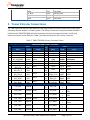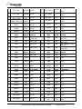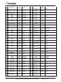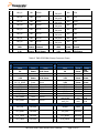
1
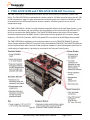
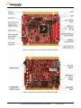
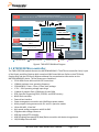
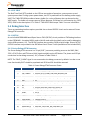
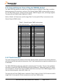
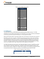
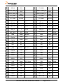
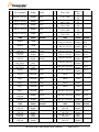
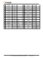
TWR-K70F120M Tower Module User's Manual Rev. 1.2 Freescale Semiconductor Inc. Table of Contents 1 TWR-K70F120M and TWR-K70F120M-KIT Overview ...............................................................5 1.1 Contents .................................................................................................................................................................................. 6 1.2 Features .................................................................................................................................................................................. 6 1.3 Getting Started ..................................................................................................................................................................... 8 1.4 Reference Documents ....................................................................................................................................................... 8 2 Hardware Description ...........................................................................................................................8 2.1 K70FN1M0 Microcontroller ........................................................................................................................................... 9 2.2 Clocking ............................................................................................................................................................................... 10 2.3 System Power .................................................................................................................................................................... 10 2.3.1 RTC VBAT ........................................................................................................................................................................................... 11 2.4 Debug Interface ................................................................................................................................................................ 11 2.4.1 OSJTAG ................................................................................................................................................................................................. 11 2.4.2 Cortex Debug+ETM Connector .................................................................................................................................................. 11 2.5 Graphical LCD Interface ................................................................................................................................................ 12 2.6 DDR2 Memory ................................................................................................................................................................... 12 2.7 NAND Flash ........................................................................................................................................................................ 12 2.8 Infrared Port ...................................................................................................................................................................... 12 2.9 Accelerometer ................................................................................................................................................................... 12 2.10 Potentiometer, Pushbuttons, LEDs ........................................................................................................................ 12 2.11 General Purpose Tower Plug-in (TWRPI) Socket ............................................................................................ 13 2.12 Touch Interface .............................................................................................................................................................. 13 2.13 Ethernet ............................................................................................................................................................................ 14 2.14 USB ...................................................................................................................................................................................... 15 2.14.1 FS/LS USB ........................................................................................................................................................................................ 15 2.14.2 HS USB ............................................................................................................................................................................................... 15 2.15 Secure Digital Card Slot .............................................................................................................................................. 15 2.16 External Bus Interface – FlexBus ............................................................................................................................ 15 3 Jumper Table.......................................................................................................................................... 16 4 Input/Output Connectors and Pin Usage Table ......................................................................... 17 5 Tower Elevator Connections ............................................................................................................ 19 TWR-K70F120M Tower Module User's Manual Page 2 of 25 List of Figures Figure 1. Freescale Tower System Overview .............................................................................................. 5 Figure 2. Callouts on front side of the TWR-K70F120M ............................................................................. 7 Figure 3. Callouts on back side of the TWR-K70F120M.............................................................................. 7 Figure 4. TWR-K70F120M Block Diagram ................................................................................................... 9 List of Tables Table 1. Cortex Debug+ETM Connector Pinout ........................................................................................ 11 Table 2. General Purpose TWRPI socket pinout ....................................................................................... 13 Table 3. Touch TWRPI socket pinout ........................................................................................................ 14 Table 4. Ethernet operation jumper settings ........................................................................................... 14 Table 5. TWR-K70F120M Jumper Table .................................................................................................... 16 Table 6. I/O Connectors and Pin Usage Table........................................................................................... 17 Table 7. TWR-K70F120M Primary Connector Pinout ............................................................................... 19 Table 8. TWR-K70F120M Primary Connector Pinout ............................................................................... 22 Revision History Revision 0.1 Date Nov 17, 2011 1.0 Dec 2, 2011 1.1 Nov 20, 2012 Changes Initial Release for PWA 700-27166 Rev B Removed references to J18 and added info on using J19 to replace J18’s functionality. Added information on running EVB at 150MHz Added jumper details for rev C board Added information on using trace TWR-K70F120M Tower Module User's Manual Page 3 of 25 1.2 May 29, 2014 Updated USB section to include instruction for connections to allow for USB OTG testing. TWR-K70F120M Tower Module User's Manual Page 4 of 25 1 TWR-K70F120M and TWR-K70F120M-KIT Overview The TWR-K70F120M is a development board for the K61 and K70 family 32-bit ARM® Cortex™-M4 MCUs. The TWR-K70F120M is populated with a device rated for 120 MHz operation across the full -40C to 85C temperature range. At room temperatures the board can be over-clocked to 150 MHz to allow for evaluation of the K70 and K61 devices that are rated for 150 MHz operation across the full temperature range. The TWR-K70F120M is a Tower Controller Module compatible with the Freescale Tower System. It can function as a stand-alone, low-cost platform for the evaluation of the Kinetis K10, K20, K6x, and K70 family of microcontroller (MCU) devices. The TWR-K70F120M features the Kinetis K70 low-power microcontroller based on the ARM® Cortex™-M4 architecture with graphical LCD controller, tamper detection, USB 2.0 HS Controller, USB 2.0 full-speed OTG controller and 10/100 Mbps Ethernet MAC. The TWR-K70F120M is available as a stand-alone product or as a kit (TWR-K70F120M-KIT) with the Tower Elevator Modules (TWR-ELEV) and the Tower Serial Module (TWR-SER). The TWR-K70F120M can also be combined with other Freescale Tower peripheral modules to create development platforms for a wide variety of applications. 0 provides an overview of the Freescale Tower System. Figure 1. Freescale Tower System Overview TWR-K70F120M Tower Module User's Manual Page 5 of 25 1.1 Contents The TWR-K70F120M contents include: TWR-K70F120M board assembly 3ft USB cable Interactive DVD with software installers and documentation Quick Start Guide The TWR-K70F120M-KIT contains: TWR-K70F120M MCU module TWR-ELEV – Primary and Secondary Elevator Modules TWR-SER – Serial module including USB host/device/OTG, Ethernet, CAN, RS232 and RS485 1.2 Features Figure 2 and Figure 3 show the TWR-K70F120M with some of the key features called out. The following list summarizes the features of the TWR-K70F120M Tower MCU Module: Tower compatible microcontroller module MK70FN1M0VMJ12: K70FN1M in a 256 MAPBGA with 120 MHz operation Touch Tower Plug-in Socket General purpose Tower Plug-in (TWRPI) socket On-board JTAG debug circuit (OSJTAG) with virtual serial port 1Gb of DDR2 SDRAM memory 2Gb of SLC NAND flash memory Three axis accelerometer (MMA8451Q) Four (4) user-controllable LEDs Four (4) capacitive touch pads Two (2) user pushbutton switches Potentiometer Battery Holder for 20mm lithium battery (e.g. 2032, 2025) Micro-SD Card slot TWR-K70F120M Tower Module User's Manual Page 6 of 25 Figure 2. Callouts on front side of the TWR-K70F120M Figure 3. Callouts on back side of the TWR-K70F120M TWR-K70F120M Tower Module User's Manual Page 7 of 25 1.3 Getting Started Follow the Quick Start Guide found printed in the TWR-K70F120M box or the interactive DVD for the list of recommended steps for getting started. There are also lab walk-through guides available on the tool support page for the TWR-K70F120M: http://www.freescale.com/TWR-K70F120M. 1.4 Reference Documents The documents listed below should be referenced for more information on the Kinetis family, Tower System, and MCU Modules. These can be found in the documentation section of freescale.com/TWRK70F120M or freescale.com/kinetis. TWR-K70F120M-QSG: Quick Start Guide TWR-K70F120M-SCH: Schematics TWR-K70F120M-PWB: Design Package K70 Family Product Brief K70 Family Reference Manual Tower Configuration Tool 2 Hardware Description The TWR-K70F120M is a Tower Controller Module featuring the MK70FN1M0VMJ12—an ARM CortexM4 based microcontroller with graphical LCD controller, tamper detection, USB 2.0 HS Controller, USB 2.0 full-speed OTG controller and 10/100 Mbps Ethernet MAC in a 256 MAPBGA package with a maximum core operating frequency of 120MHz. It is intended for use in the Freescale Tower System but can operate stand-alone. An on-board debug circuit, OSJTAG, provides a JTAG debug interface and a power supply input through a single USB mini-AB connector. Figure 4 shows a block diagram of the TWR-K70F120M. The following sections describe the hardware in more detail. TWR-K70F120M Tower Module User's Manual Page 8 of 25 Tower Elevator Expansion Connectors SDHC, I2S, SPI, I2C, ADC, USB, DAC, PWM, UARTs, Flexbus, Ethernet, LCD, and ULPI 5.0V 50 MHz OSC 32.768 KHz XTAL 12 MHz XTAL IR Output Comparator 5.0V USB Mini-B OSJTAG JTAG, Power, SCI K70FN1M0 256 MAPBGA GPIO / Interrupts VBAT (RTC) LED DDR Controller SPI, I2C, ADC, GPIO ADC LED SDHC MMA8451Q LED LED Reset uSD Card Slot Infrared Port JTAG SCI Battery Holder 3.3V TSI, GPIO Capacitive Touch Pads NFC/FlexBus General Purpose Tower Plug-in (TWRPI) 2Gb NAND Flash 2 IC Freescale Device External Connectors Touch Tower Plug-in (TWRPI) 1Gb DDR2 Interface Circuits Power Memory Figure 4. TWR-K70F120M Block Diagram 2.1 K70FN1M0 Microcontroller The TWR-K70F120M module features the MK70FN1M0VMJ12. The K70 microcontroller family is part of the Kinetis portfolio of devices built around an ARM Cortex-M4 core. Refer to the K70 Family Product Brief and the K70 Family Reference Manual for comprehensive information on the MK70FN1M0VMJ12 device. The key features are listed here: 32-bit ARM Cortex-M4 core with DSP instructions 120MHz maximum core operating frequency 256 MAPBGA, 17mm x 17mm, 1.0mm pitch package 1.71V – 3.6V operating voltage input range 1 Mbyte of program flash, 128 Kbytes of static RAM DDR controller supporting DDR1, LPDDR1, and DDR2 memory NAND flash controller External bus interface Power management controller with 10 different power modes Multi-purpose clock generator with PLL and FLL operation modes 16-bit SAR ADC, 12-bit DAC High-speed analog comparator with 6-bit DAC Programmable voltage reference USB high-speed OTG controller USB full-speed/low-speed OTG/Host/Device controller with device charge detect 10/100 Mbps Ethernet MAC TWR-K70F120M Tower Module User's Manual Page 9 of 25 SPI, I2C (w/ SMBUS support), UART (w/ ISO7816, CEA709.1-B (LON), and IrDA support), CAN, I2S SD Host Controller (SDHC) GPIO with pin interrupt support, DMA request capability, digital glitch filtering Capacitive touch sensing inputs (TSI) Debug interfaces: JTAG, cJTAG, SWD Trace: TPIO, FPB, DWT, ITM, ETM, ETB 2.2 Clocking The Kinetis MCUs start up from an internal digitally controlled oscillator (DCO). Software can enable one, two, or three external oscillators if desired. Two of the external oscillators provide clocks to the Multipurpose Clock Generator (MCG) module and can range from 32.768 KHz up to a 32 MHz crystal or ceramic resonator. The external oscillator for the Real Time Clock (RTC) module accepts a 32.768 kHz crystal. The EXTAL0 and EXTAL1 pins of the main external oscillators can also be driven directly from an external clock source. The TWR-K70F120M features a 50 MHz on-board clock oscillator connected to EXTAL0 as seen in sheet 4 of the schematics. However, when the K70 Ethernet MAC is operating in RMII mode, synchronization of the MCU input clock and the 50 MHz RMII transfer clock is important. In this mode, the MCU input clock must be kept in phase with the 50 MHz clock supplied to the external PHY. Therefore, the TWR-K70F120M provides the option (see jumper description in Table 5) to select the clock input to the MCU from 1) the on-board 50MHz source or 2) an external clock from the CLKIN0 pin on the Primary Connector. When the K70 is operating in Ethernet RMII mode, the Tower peripheral module implementing the RMII PHY device should drive a 50 MHz clock on the CLKIN0 signal that is kept in phase with the clock supplied to the RMII PHY. Refer to section 2.13 “Ethernet” for more information. The TWR-K70F120M also includes a 12MHz crystal connected to EXTAL1/XTAL1. 2.3 System Power In stand-alone operation, the main power source for the TWR-K70F120M module is derived from the 5.0V input from either the USB mini-B connector, J13, or the debug header, J11, when a shunt is placed on jumper J12. A low-dropout regulator provides a 3.3V supply from the 5.0V input voltage. Refer to sheet 6 of the TWR-K70F120M schematics for more details. When installed into a Tower System, the TWR-K70F120M can be powered from either an on-board source or from another source in the assembled Tower System. If both the on-board and off-board sources are available, the TWR-K70F120M will default to the off-board source. The 3.3V power supplied to the MCU is routed through two jumpers, J8 and J20. J8 can be supplies VDD to the processor and also VDD_INT as long as J20 is installed. J20 supplies VDD_INT to the processor. The jumper shunts can be removed to allow for either 1) alternate MCU supply voltages to be injected or 2) the measurement of power consumed by the MCU. TWR-K70F120M Tower Module User's Manual Page 10 of 25 2.3.1 RTC VBAT The Real Time Clock (RTC) module on the K70 has two modes of operation, system power-up and system power-down. During system power-down, the RTC is powered from the backup power supply, VBAT. The TWR-K70F120M provides a battery holder for a coin cell battery that can be used as the VBAT supply. The holder can accept common 20mm diameter 3V lithium coin cell batteries (e.g. 2032, 2025). Refer to the description J17 in Table 5 “TWR-K70F120M Jumper Table” for more information. 2.4 Debug Interface There are two debug interface options provided: the on-board OSJTAG circuit and an external Cortex Debug+ETM connector. 2.4.1 OSJTAG An on-board MC9S08JM60 based Open Source JTAG (OSJTAG) circuit provides a JTAG debug interface to the K70FN1M0. A standard USB A male to Mini-B male cable (provided) can be used for debugging via the USB connector, J13. The OSJTAG interface also provides a USB to serial bridge. Drivers for the OSJTAG interface are provided in the P&E Micro Kinetis Tower Toolkit (available on the included DVD). 2.4.2 Cortex Debug+ETM Connector The Cortex Debug+ETM connector is a 20-pin (0.05") connector providing access to the SWD, SWV, JTAG, cJTAG, EzPort and ETM trace (4-bit) signals available on the K70 device. The pinout and K70 pin connections to the debug connector, J11, is shown in Table 1Table 1. NOTE: The TRACE_CLKOUT signal is not connected to the debug connector by default. In order to use trace functionality R137 should be populated and R138 and R11 should be removed. Table 1. Cortex Debug+ETM Connector Pinout Pin 1 2 3 4 5 6 7 8 9 10 11 12 13 14 15 16 17 Function VTref TMS / SWDIO GND TCK / SWCLK GND TDO / SWO Key TDI GNDDetect nRESET Target Power TRACECLK Target Power TRACEDATA[0] GND TRACEDATA[1] GND TWR-K70F120M Connection 3.3V MCU supply (P3V3_MCU) PTA3/SCI0_RTS_b/FTM0_CH0/JTAG_MS/SWD_DIO GND PTA0/SCI0_CTS_b/FTM0_CH5/JTAG_CLK/SWD_CLK/EZP_CLK GND PTA2/SCI0_TX/FTM0_CH7/JTAG_DO/TRACE_SWO/EZP_DO ― PTA1/SCI0_RX/FTM0_CH6/JTAG_DI/EZP_DI PTA4/FTM0_CH1/MS/NMI_b/EZP_CS_b RESET_b 5V supply (via J12) PTA6/FTM0_CH3/TRACE_CLKOUT 5V supply (via J12) PTA10/FTM2_CH0/FTM2_QD_PHA/TRACE_D0 GND PTA9/FTM1_CH1/FTM1_QD_PHB/TRACE_D1 GND TWR-K70F120M Tower Module User's Manual Page 11 of 25 Pin 18 19 20 Function TRACEDATA[2] GND TRACEDATA[3] TWR-K70F120M Connection PTA8/FTM1_CH0/FTM1_QD_PHA/TRACE_D2 GND PTA7/FTM0_CH4/TRACE_D3 Note: Many of the trace signals connected to the debug connector are also connected elsewhere on the TWR-K70F120M. Refer to Table 6 “I/O Connectors and Pin Usage Table” and Table 7 “TWRK70F120M Primary Connector Pinout” for more information. 2.5 Graphical LCD Interface The K70FN1M0 processor includes an on-chip graphical LCD controller module. The module is not used directly on the TWR-K70F120M board, but the LCD signals are routed to the Secondary connector, allowing the connection to an external LCD or additional circuitry on a Tower peripheral module. The TWR-LCD-RGB will provide an LCD panel and all required external circuitry so that it can interface directly to the TWR-K70F120M. This is an easy way to evaluate the graphical LCD module on the K70 processor. 2.6 DDR2 Memory The TWR-K70F120M includes 1Gb of DDR2 memory (MT47H64M16HR-25). The board also includes a DDR regulator that provides the main 1.8V supply for the memory and the processors SDRAM pads as well as VTT and VREF voltages. 2.7 NAND Flash The TWR-K70F120M includes 2Gb of SLC NAND flash memory (MT29F2G15ABAEAWP). The data lines used for the NAND flash are shared between the NAND flash controller and the FlexBus interface. Internal arbitration logic in the processor allows for dynamic sharing between the NAND flash and FlexBus interfaces. 2.8 Infrared Port An infrared transmit and receive interface is implemented on the board. The CMT_IRO pin directly drives an infrared diode. The receiver uses an infrared phototransistor connected to an on-chip analog comparator through a low-pass filter. Internal to the K70 device, the output of the analog comparator can be routed to a UART module for easier processing of the incoming data stream. 2.9 Accelerometer An MMA8451Q digital accelerometer is connected to the K70 MCU through an I2C interface and a GPIO/IRQ signal. Refer to Table 6 “I/O Connectors and Pin Usage Table” for connection details. 2.10 Potentiometer, Pushbuttons, LEDs The TWR-K70F120M features two pushbutton switches connected to GPIO/interrupt signals, one pushbutton connected to the master reset signal, four capacitive touch pad electrodes, four usercontrollable LEDs, and a potentiometer connected to an ADC input signal. Refer to Table 6 “I/O Connectors and Pin Usage Table” for information about which port pins are connected to these features. TWR-K70F120M Tower Module User's Manual Page 12 of 25 2.11 General Purpose Tower Plug-in (TWRPI) Socket The TWR-K70F120M features a socket that can accept a variety of different Tower Plug-in modules featuring sensors, RF transceivers, and more. The General Purpose TWRPI socket provides access to I2C, SPI, IRQs, GPIOs, timers, analog conversion signals, TWRPI ID signals, reset, and voltage supplies. The pinout for the TWRPI Socket is defined in Table 2. Refer to Table 6 “I/O Connectors and Pin Usage Table” for the specific K70 pin connections to the General Purpose TWRPI socket. Table 2. General Purpose TWRPI socket pinout Left-side 2x10 Connector Pin Description 1 5V VCC 2 3.3 V VCC 3 GND 4 3.3V VDDA 5 VSS (Analog GND) 6 VSS (Analog GND) 7 VSS (Analog GND) 8 ADC: Analog 0 9 ADC: Analog 1 10 VSS (Analog GND) 11 VSS (Analog GND) 12 ADC: Analog 2 13 VSS (Analog GND) 14 VSS (Analog GND) 15 GND 16 GND 17 ADC: TWRPI ID 0 18 ADC: TWRPI ID 1 19 GND 20 Reset Right-side 2x10 Connector Pin Description 1 GND 2 GND 3 I2C: SCL 4 I2C: SDA 5 GND 6 GND 7 GND 8 GND 9 SPI: MISO 10 SPI: MOSI 11 SPI: SS 12 SPI: CLK 13 GND 14 GND 15 GPIO: GPIO0/IRQ 16 GPIO: GPIO1/IRQ 17 GPIO: GPIO2 18 GPIO: GPIO3 19 GPIO: GPIO4/Timer 20 GPIO: GPIO5/Timer 2.12 Touch Interface The touch sensing input (TSI) module of the Kinetis MCUs provides capacitive touch sensing detection with high sensitivity and enhanced robustness. Each TSI pin implements the capacitive measurement of an electrode. The TWR-K70F120M provides two methods for evaluating the TSI module. There are four individual electrodes on-board the TWR-K70F120M that simulate pushbuttons. Additionally, twelve TSI signals are connected to a Touch Tower Plug-in (TWRPI) socket that can accept Touch TWRPI daughter cards that may feature keypads, rotary dials, sliders, etc. The pinout for the Touch TWRPI socket is defined in Table 3. Refer to Table 6 “I/O Connectors and Pin Usage Table” for the specific K70 pin connections to the Touch TWRPI socket. TWR-K70F120M Tower Module User's Manual Page 13 of 25 Table 3. Touch TWRPI socket pinout Pin 1 2 3 4 5 6 7 8 9 10 11 12 13 14 15 16 17 18 19 20 Description 5V VCC 3.3 V VCC Electrode 0 3.3V VDDA Electrode 1 VSS (Analog GND) Electrode 2 Electrode 3 Electrode 4 Electrode 5 Electrode 6 Electrode 7 Electrode 8 Electrode 9 Electrode 10 Electrode 11 ADC: TWRPI ID 0 ADC: TWRPI ID 1 GND Reset 2.13 Ethernet The K70FN1M0 features a 10/100 Mbps Ethernet MAC with MII and RMII interfaces. The TWRK70F120M routes the RMII interface signals from the K70 MCU to the Primary Connector, allowing the connection to an external Ethernet PHY device on a Tower peripheral module. When the K70 Ethernet MAC is operating in RMII mode, synchronization of the MCU clock and the 50 MHz RMII transfer clock is important. The MCU input clock must be kept in phase with the 50 MHz clock supplied to the external PHY. Therefore, the TWR-K70F120M provides the option (see jumper descriptions Table 5) to clock the MCU from an external clock from the CLKIN0 pin on the Primary Connector. The Tower peripheral module implementing the RMII PHY device should drive a 50 MHz clock on the CLKIN0 pin that is kept in phase with the clock supplied to the RMII PHY. The TWR-SER module that comes as part of the TWR-K70F120M-KIT provides a 10/100 Ethernet PHY that can operate in either MII or RMII mode. By default the PHY is boot strapped to operate in MII mode; therefore jumper configuration changes may be required. Table 4 shows the settings for proper interoperability between the Ethernet interface on the TWR-SER and the TWR-K70F120M. Table 4. Ethernet operation jumper settings Tower Module TWR-K70F120M(rev B) TWR-K70F120M(rev C) Jumper J19 J18 Setting OFF ON TWR-K70F120M Tower Module User's Manual Page 14 of 25 TWR-SER TWR-SER TWR-SER J2 J3 J12 3-4 2-3 9-10 2.14 USB The K70FN1M0 features two different USB modules--a USB full-speed/low-speed OTG/Host/Device controller with built-in transceiver and a high-speed OTG/Host/Device controller that requires a external ULPI PHY. 2.14.1 FS/LS USB The TWR-K70F120M routes the USB D+ and D- signals from the K70 MCU to the Primary Connector, allowing the connection to external USB connectors or additional circuitry on a Tower peripheral module. The TWR-SER module included as part of the TWR-K70F120M-KIT provides a USB OTG/Host/Device interface with a mini-AB USB connector. There are many configuration options that can be selected to evaluate different USB modes of operation. By default, the TWR-SER is configured for USB Device operation. Please refer to the documentation included with the TWR-SER for more information on the configuration options. Note: In order to use the USB module in true OTG mode, VREGIN must be powered before the USB cable is plugged in. By default the board does not support this. The board can be modified by removing the jumper on J1, then directly connecting P5V_ELEV (or another 5V net that will be active during testing) to pin1 of J1 so that VREGIN has a 5V supply independent of the USB port on the TWR-SER board. 2.14.2 HS USB The TWR-K70F120M routes the ULPI interface signals for the high-speed USB module to the Secondary Connector allowing the connection to an external ULPI PHY or additional circuitry on a Tower peripheral module. The TWR-SER2 module includes a ULPI PHY that can be used with the TWR-K70F120M in order to evaluate the high-speed USB functionality. The TWR-SER2 is not included as part of the TWRK70F120M-KIT, but the boards can be ordered individually from Freescale. 2.15 Secure Digital Card Slot A Micro-Secure Digital (SD) card slot is available on the TWR-K70F120M connected to the SD Host Controller (SDHC) signals of the K70 MCU. This slot will accept micro-SD memory cards. Refer to Table 6 “I/O Connectors and Pin Usage Table” for the SDHC signal connection details. 2.16 External Bus Interface – FlexBus The K70 device features a multi-function external bus interface called the FlexBus interface controller capable of interfacing to slave-only devices. The FlexBus interface is not used directly on the TWRK70F120M. Instead, a subset of the FlexBus is connected to the Primary Connector so that the external TWR-K70F120M Tower Module User's Manual Page 15 of 25 bus can access devices on Tower peripheral modules. Refer to Table 7 “TWR-K70F120M Primary Connector Pinout” and sheet 8 of the TWR-K70F120M schematics for more details. 3 Jumper Table There are several jumpers on the TWR-K70F120M that provide configuration selection and signal isolation. Refer to the following table for details. The default installed jumper settings are shown in bold with asterisks. Table 5. TWR-K70F120M Jumper Table Jumper J1 Option USB VREGIN Power Connection J2 Infrared Transmitter Connection J8 MCU Power Connection Setting *ON* OFF ON *OFF* *ON* J10 OSJTAG Mode Selection OFF ON *OFF* ON J12 JTAG Power Connection *OFF* ON J16 J17 Infrared Receiver Connection Description Connect USB0_VBUS from Primary Elevator (A57) to VREGIN Disconnect VREGIN from Primary Elevator Connect PTD7/CMT_IRO/UART0_TX to IR Transmitter (D1) Disconnect PTD7/CMT_IRO/UART0_TX from IR Transmitter (D1) Connect on-board 3.3V supply to MCU Isolate MCU from power supply (allows for external supply or power measurements) OSJTAG bootloader mode (OSJTAG firmware reprogramming) Debugger mode Connect on-board 5V supply to JTAG port (supports powering board from external JTAG probe) Disconnect on-board 5V supply from JTAG port Connect DAC1_OUT/CMP2_IN3 to IR Receiver *OFF* Disconnect DAC1_OUT/CMP2_IN3 to IR Receiver *1-2* Connect VBAT to on-board 3.3V supply VBAT Power Selection 2-3 Connect VBAT to the higher voltage between on-board 3.3V supply or coin-cell supply On-board 50MHz oscillator disabled. Off-board clock drives main EXTAL. J18 (revC board) 50 MHz oscillator output enable ON *OFF* NOTE: This option should be selected whenever a tower module card that provides a clock on primary elevator pin B24 is connected to the CPU module. Otherwise there will be contention between the two clock sources. On-board 50MHz oscillator enabled. On-board 50 MHz clock drives main EXTAL. TWR-K70F120M Tower Module User's Manual Page 16 of 25 J19 (revC board) *ON* Power supply to 50MHz oscillator enabled. OFF Power supply to 50MHz oscillator disabled. 50 MHz oscillator power *ON* J19 (revB board) 50MHz clock disable. J20 MCU VDD_INT Power Connection OFF *ON* OFF On-board 50MHz oscillator enabled. On-board 50 MHz clock drives main EXTAL. On-board 50MHz oscillator disabled. Off-board clock drives main EXTAL. NOTE: This option must be selected whenever a tower module card that provides a clock on primary elevator pin B24 is connected to the CPU module. Otherwise there will be contention between the two clock sources. Connect VDD and VDD_INT rails together Isolate MCU VDD_INT from power supply (allows for external supply or power measurements) 4 Input/Output Connectors and Pin Usage Table The following table provides details on which K70FN1M0 pins are used to communicate with the LEDs, switches, and other I/O interfaces onboard the TWR-K70F120M. Note: Some port pins are used in multiple interfaces on-board and many are potentially connected to off-board resources via the Primary and Secondary Connectors. Take care to avoid attempted simultaneous usage of mutually exclusive features. Table 6. I/O Connectors and Pin Usage Table Feature OSJTAG USB-toserial Bridge SD Card Slot Infrared Port Pushbuttons Touch Pads Connection OSJTAG Bridge RX Data OSJTAG Bridge TX Data SD Clock SD Command SD Data0 SD Data1 SD Data2 SD Data3 SD Card Detect IR Transmit IR Receive SW1 (IRQ0) SW2 (IRQ1) SW3 (RESET) E1 / Touch E2 / Touch E3 / Touch E4 / Touch Port Pin PTE17 PTE16 PTE2 PTE3 PTE1 PTE0 PTE5 PTE4 PTE28 PTD7 ― PTD0 PTE26 RESET_b PTA4 PTB3 PTB2 PTB16 Pin Function UART2_RX UART2_TX SDHC0_DCLK SDHC0_CMD SDHC0_D0 SDHC0_D1 SDHC0_D2 SDHC0_D3 PTE28 CMT_IRO CMP2_IN3 PTD0 PTE26 RESET_b TSI0_CH5 TSI0_CH8 TSI0_CH7 TSI0_CH9 TWR-K70F120M Tower Module User's Manual Page 17 of 25 LEDs Potentiometer Accelerometer General Purpose TWRPI Socket Touch Pad / Segment LCD TWRPI Socket I2S/SAI Header E1 / Orange LED E2 / Yellow LED E3 / Green LED E4 / Blue LED Potentiometer (R71) I2C SDA I2C SCL INT1 INT2 TWRPI AN0 (J4 Pin 8) TWRPI AN1 (J4 Pin 9) TWRPI AN2 (J4 Pin 12) TWRPI ID0 (J4 Pin 17) TWRPI ID1 (J4 Pin 18) TWRPI I2C SCL (J5 Pin 3) TWRPI I2C SDA (J5 Pin 4) TWRPI SPI MISO (J5 Pin 9) TWRPI SPI MOSI (J5 Pin 10) TWRPI SPI SS (J5 Pin 11) TWRPI SPI CLK (J5 Pin 12) TWRPI GPIO0 (J5 Pin 15) TWRPI GPIO1 (J5 Pin 16) TWRPI GPIO2 (J5 Pin 17) TWRPI GPIO3 (J5 Pin 18) TWRPI GPIO4 (J5 Pin 19) Electrode 0 (J3 Pin 3) Electrode 1 (J3 Pin 5) Electrode 2 (J3 Pin 7) Electrode 3 (J3 Pin 8) Electrode 4 (J3 Pin 9) Electrode 5 (J3 Pin 10) Electrode 6 (J3 Pin 11) Electrode 7 (J3 Pin 12) Electrode 8 (J3 Pin 13) Electrode 9 (J3 Pin 14) Electrode 10 (J3 Pin 15) Electrode 11 (J3 Pin 16) TWRPI ID0 (J3 Pin 17) TWRPI ID1 (J3 Pin 18) RX_FS TX_FS TXD0 PTA11 PTA28 PTA29 PTA10 ― PTE18 PTE19 PTB4 PTB7 ― ― ― ― ― PTE19 PTE18 PTD14 PTA11 PTA28 PTA29 PTA10 ADC1_DM1 I2C0_SDA I2C0_SCL PTB4 PTB7 ADC0_DP0/ADC1_DP3 ADC0_DM0/ADC1_DM3 ADC1_DP0/ADC0_DP3 ADC0_DP1/ADC2_DP0/ADC3_DP3 ADC0_DM1/ADC2_DM0/ADC3_DM3 I2C0_SCL I2C0_SDA SPI2_SIN PTD13 PTD15 PTD12 PTB4 PTB8 PTB9 PTA19 PTE26 PTB0 PTB1 PTB2 PTB3 PTC0 PTC1 PTC2 PTA4 PTB16 PTB17 PTB18 PTB19 ― ― PTE8 PTE11 PTE10 SPI2_SOUT SPI2_PCS1 SPI2_SCK PTB4 PTB8 PTB9 PTA19 PTE26 TSI0_CH0 TSI0_CH6 TSI0_CH7 TSI0_CH8 TSI0_CH13 TSI0_CH14 TSI0_CH15 TSI0_CH5 TSI0_CH9 TSI0_CH10 TSI0_CH11 TSI0_CH12 ADC1_DP1 ADC1_SE16 I2S0_RX_FS I2S0_TX_FS I2S0_TXD0 TWR-K70F120M Tower Module User's Manual Page 18 of 25 RXD0 RX_BCLK TX_BCLK PTE7 PTE9 PTE12 I2S0_RXD0 I2S0_RX_BCLK I2S0_TX_BCLK MCLK PTE6 I2S0_MCLK 5 Tower Elevator Connections The TWR-K70F120M features two expansion card-edge connectors that interface to the Primary and Secondary Elevator boards in a Tower system. The Primary Connector (comprised of sides A and B) is utilized by the TWR-K70F120M while the Secondary Connector (comprised of sides C and D) only makes connections to the GND pins. Table 7 provides the pinout for the Primary Connector. Table 7. TWR-K70F120M Primary Connector Pinout Pi n # B1 B2 B3 B4 B5 B6 B7 B8 B9 B1 0 B1 1 B1 2 B1 3 B1 4 B1 5 B1 6 B1 7 B1 8 Side B Name 5V GND 3.3V Group Power Power Power ELE_PS_SENSE GND GND SDHC_CLK / SPI1_CLK SDHC_D3 / SPI1_CS1_b SDHC_D3 / SPI1_CS0_b SDHC_CMD / SPI1_MOSI SDHC_D0 / SPI1_MISO Power Power Power SDHC / SPI 1 SDHC / SPI 1 SDHC / SPI 1 SDHC / SPI 1 SDHC / SPI 1 ETH_COL Ethernet ETH_RXER Ethernet ETH_TXCLK Ethernet ETH_TXEN Ethernet ETH_TXER Ethernet ETH_TXD3 Ethernet ETH_TXD2 Ethernet TWR-K70F120M Primary Connector Pi n Usage # Name 5.0V Power A1 5V Ground A2 GND 3.3V Power A3 3.3V Elevator Power Sense A4 3.3V Ground A5 GND Ground A6 GND PTE2 A7 A8 PTE4 PTE3 PTE1 PTA5 PTA15 A9 A1 0 A1 1 A1 2 A1 3 A1 4 A1 5 A1 6 A1 7 A1 8 Side A Group Power Power Power Usage 5.0V Power Ground 3.3V Power Power Power Power 3.3V Power Ground Ground SCL0 I2C 0 PTE19 SDA0 I2C 0 PTE18 GPIO9 / CTS1 GPIO8 / SDHC_D2 GPIO7 / SD_WP_DET GPIO / UART GPIO / SDHC GPIO / SDHC ETH_CRS ETH_MDC ETH_MDIO ETH_RXCLK ETH_RXDV ETH_RXD3 ETH_RXD2 TWR-K70F120M Tower Module User's Manual Etherne t Etherne t Etherne t Etherne t Etherne t Etherne t Etherne t PTE18 PTE5 PTE27 PTB1 PTB0 PTA14 Page 19 of 25 B1 9 B2 0 B2 1 B2 2 B2 3 B2 4 B2 5 B2 6 B2 7 B2 8 B2 9 B3 0 B3 1 B3 2 B3 3 B3 4 B3 5 B3 6 B3 7 B3 8 B3 9 B4 0 B4 1 B4 2 B4 3 B4 4 B4 5 ETH_TXD1 Ethernet PTA17 ETH_TXD0 Ethernet PTA16 GPIO2 / SDHC_D1 GPIO / UART GPIO / SDHC GPIO3 GPIO PTE28 CLKIN0 Clock PTA18 CLKOUT1 Clock PTE26 GND Power AN7 ADC AN6 ADC ADC0_DM1 AN5 ADC ADC1_DP1 AN4 ADC ADC1_DM1 GND Power DAC1 DAC TMR3 Timer TMR2 Timer PTD6 GPIO4 GPIO PTB8 3.3V Power PWM7 PWM PTA2 PWM6 PWM PTA1 PWM5 PWM PTD5 PWM4 PWM PTA7 CANRX0 CAN 0 PTC16 CANTX0 CAN 0 PTC17 1WIRE 1-Wire SPI0_MISO SPI 0 PTD14 SPI0_MOSI SPI 0 PTD13 GPIO1 / RTS1 PTE19 PTE0 Ground ADC0_DP1 Ground DAC1_OUT 3.3V Power A1 9 A2 0 A2 1 A2 2 A2 3 A2 4 A2 5 A2 6 A2 7 A2 8 A2 9 A3 0 A3 1 A3 2 A3 3 A3 4 A3 5 A3 6 A3 7 A3 8 A3 9 A4 0 A4 1 A4 2 A4 3 A4 4 A4 5 ETH_RXD1 ETH_RXD0 Etherne t Etherne t PTA12 PTA13 SSI_MCLK SSI SSI_BCLK SSI SSI_FS SSI SSI_RXD SSI SSI_TXD SSI GND Power AN3 ADC AN2 ADC AN1 ADC AN0 ADC GND Power DAC0 DAC TMR1 Timer PTA9 TMR0 Timer PTA8 GPIO6 GPIO PTB9 3.3V Power PWM3 PWM PTA6 PWM2 PWM PTC3 PWM1 PWM PTC2 PWM0 PWM PTC1 RXD0 UART 0 PTF7 TXD0 UART 0 PTF8 RXD1 UART 1 PTE17 TXD1 UART 1 PTE16 VSS Analog Vref VSSA TWR-K70F120M Tower Module User's Manual PTE6 PTE12 PTE11 PTE7 PTE10 Ground PGA0_DP/ADC0_DP0/A DC1_DP3 PGA0_DM/ADC0_DM0/ ADC1_DM3 PGA1_DP/ADC1_DP0/A DC0_DP3 PGA1_DM/ADC1_DM0/ ADC0_DM3 Ground DAC0_OUT 3.3V Power Page 20 of 25 B4 6 B4 7 B4 8 B4 9 B5 0 B5 1 B5 2 B5 3 B5 4 B5 5 B5 6 B5 7 B5 8 B5 9 B6 0 B6 1 B6 2 B6 3 B6 4 B6 5 B6 6 B6 7 B6 8 B6 9 B7 0 B7 1 B7 2 SPI0_CS0_b SPI 0 PTD11 SPI0_CS1_b SPI 0 PTD15 SPI0_CLK SPI 0 PTD12 GND Power SCL1 I2C 1 PTE19 SDA1 I2C 1 PTE18 GPIO5 / SD_CARD_DET GPIO / SDHC PTE28 USB0_DP_PDOWN USB0_DM_PDOW N USB 0 IRQ_H Interrupt IRQ_G Interrupt IRQ_F Interrupt IRQ_E Interrupt IRQ_D Interrupt PTB6 IRQ_C Interrupt PTB6 IRQ_B Interrupt PTB7 IRQ_A Interrupt PTB7 EBI_ALE / EBI_CS1_b EBI PTD0 EBI_CS0_b EBI PTD1 GND Power Ground USB 0 PTB4 PTB4 PTB5 PTB5 Ground EBI PTB18 EBI PTB17 EBI PTB16 EBI PTB11 EBI_AD19 EBI PTB10 EBI_R/W_b EBI PTC11 EBI_OE_b EBI PTB19 EBI_AD15 EBI_AD16 EBI_AD17 EBI_AD18 A4 6 A4 7 A4 8 A4 9 A5 0 A5 1 A5 2 A5 3 A5 4 A5 5 A5 6 A5 7 A5 8 A5 9 A6 0 A6 1 A6 2 A6 3 A6 4 A6 5 A6 6 A6 7 A6 8 A6 9 A7 0 A7 1 A7 2 VDDA Analog Vref CANRX1 CAN 1 CANTX1 CAN 1 GND Power GPIO14 GPIO GPIO15 GPIO GPIO16 GPIO GPIO17 GPIO USB0_DM USB0_DP USB0_ID USB0_VBUS USB 0 USB 0 VDDA Ground USB0_DM USB0_DP USB 0 USB 0 VREGIN I2S0_DIN_SC K I2S I2S0_DIN_WS I2S I2S0_DIN1 I2S I2S0_DOUT1 I2S RSTIN_b Reset RESET_b RSTOUT_b Reset PTB8 CLKOUT0 Clock PTC3 GND Power EBI_AD14 EBI_AD13 EBI_AD12 EBI_AD11 EBI_AD10 EBI_AD9 EBI_AD8 TWR-K70F120M Tower Module User's Manual PTE9 PTE8 PTE8 PTE9 Ground EBI PTC0 EBI PTC1 EBI PTC2 EBI PTC4 EBI PTC5 EBI PTC6 EBI PTC7 Page 21 of 25 B7 3 B7 4 B7 5 B7 6 B7 7 B7 8 B7 9 B8 0 B8 1 B8 2 EBI_D7 EBI PTB20 EBI_D6 EBI PTB21 EBI_D5 EBI PTB22 EBI_D4 EBI PTB23 EBI_D3 EBI PTC12 EBI_D2 EBI PTC13 EBI_D1 EBI PTC14 EBI_D0 EBI PTC15 GND Power Ground 3.3V Power 3.3V Power A7 3 A7 4 A7 5 A7 6 A7 7 A7 8 A7 9 A8 0 A8 1 A8 2 EBI_AD7 EBI_AD6 EBI_AD5 EBI_AD4 EBI_AD3 EBI_AD2 EBI_AD1 EBI_AD0 EBI PTC8 EBI PTC9 EBI PTC10 EBI PTD2 EBI PTD3 EBI PTD4 EBI PTD5 EBI PTD6 GND Power Ground 3.3V Power 3.3V Power Table 8. TWR-K70F120M Primary Connector Pinout TWR-K70F120M Secondary Connector Pi n # Name Group D1 D2 5V GND Power Power D3 3.3V Power D4 D5 D6 D7 D8 D9 D1 0 D1 1 ELE_PS_SENSE GND GND SPI2_CLK SPI2_CS1_b SPI2_CS0_b Power Power Power SPI 2 SPI 2 SPI 2 SPI2_MOSI SPI 2 PTD13 SPI2_MISO SPI 2 PTD14 ETH_COL Ethernet ETH_RXER Ethernet ETH_TXCLK Ethernet ETH_TXEN Ethernet D1 2 D1 3 D1 4 D1 5 Pi n # Name Group 5.0V Power Ground C1 C2 5V GND Power Power 3.3V Power Elevator Power Sense Ground Ground PTD12 PTD15 PTD11 C3 3.3V Power C4 C5 C6 C7 C8 C9 C1 0 C1 1 3.3V GND GND SCL2 SDA2 GPIO25 Power Power Power I2C 2 I2C 2 GPIO ULPI_STOP ULPI PTA9 ULPI_CLK ULPI PTA6 GPIO26 GPIO ETH_MDC Ethernet ETH_MDIO Ethernet ETH_RXCLK Ethernet Side D Usage C1 2 C1 3 C1 4 C1 5 Side C TWR-K70F120M Tower Module User's Manual Page 22 of 25 Usage 5.0V Power Ground 3.3V Power 3.3V Power Ground Ground PTE19 PTE18 D1 6 D1 7 D1 8 D1 9 D2 0 D2 1 D2 2 D2 3 D2 4 D2 5 D2 6 D2 7 D2 8 D2 9 D3 0 D3 1 D3 2 D3 3 D3 4 D3 5 D3 6 D3 7 D3 8 D3 9 D4 0 D4 1 D4 2 GPIO18 GPIO GPIO19 / SDHC_D4 GPIO20 / SDHC_D5 GPIO / SDHC GPIO / SDHC ETH_TXD1 Ethernet ETH_TXD0 Ethernet ULPI_NEXT / USB1_DM ULPI_DIR / USB1_DP UPLI_DATA5 / USB2_DM ULPI_DATA6 / USB2_DP ULPI / 1 ULPI / 1 ULPI / 2 ULPI / 2 USB PTA8 USB PTA7 USB PTA27 USB PTA28 ULPI_DATA7 ULPI PTA29 GND LCD_HSYNC / LCD_P24 LCD_VSYNC / LCD_P25 Power Ground Display PTF2 Display PTF3 AN13 ADC AN12 ADC GND LCD_CLK / LCD_P26 Power Ground Display PTF0 TMR11 Timer TMR10 Timer GPIO21 GPIO 3.3V Power PWM15 PWM PWM14 PWM PWM13 PWM PWM12 PWM CANRX1 CAN 1 CANTX1 CAN 1 3.3V Power C1 6 C1 7 C1 8 C1 9 C2 0 C2 1 C2 2 C2 3 C2 4 C2 5 C2 6 C2 7 C2 8 C2 9 C3 0 C3 1 C3 2 C3 3 C3 4 C3 5 C3 6 C3 7 C3 8 C3 9 C4 0 C4 1 C4 2 ETH_RXDV Ethernet GPIO27 / SDHC_D6 GPIO28 / SDHC_D7 GPIO / SDHC GPIO / SDHC ETH_RXD1 Ethernet ETH_RXD0 Ethernet ULPI_DATA0 USB3_DM ULPI_DATA1 USB3_DP ULPI_DATA2 USB4_DM ULPI_DATA3 USB4_DP / / / / ULPI / USB 3 ULPI / USB 3 ULPI / USB 4 ULPI / USB 4 ULPI_DATA4 ULPI GND Power AN11 ADC AN10 ADC AN9 ADC AN8 ADC GND Power GPIO29 GPIO TMR9 Timer TMR8 Timer GPIO30 GPIO 3.3V Power PWM11 PWM PWM10 PWM PWM9 PWM PWM8 PWM RXD2 / TSI0 TXD2 / TSI1 TWR-K70F120M Tower Module User's Manual UART 2 / TSI UART 2 / TSI Page 23 of 25 PTA10 PTA11 PTA24 PTA25 PTA26 Ground Ground 3.3V Power D4 3 D4 4 D4 5 D4 6 D4 7 D4 8 D4 9 D5 0 D5 1 D5 2 D5 3 D5 4 D5 5 D5 6 D5 7 D5 8 D5 9 D6 0 D6 1 D6 2 D6 3 D6 4 D6 5 D6 6 D6 7 D6 8 D6 9 LCD_CONTRAST Display PTC18 LCD_OE / LCD_P27 Display PTF1 LCD_D0 / LCD_P0 Display PTF4 LCD_D1 / LCD_P1 Display PTF5 LCD_D2 / LCD_P2 Display PTF6 LCD_D3 / LCD_P3 Display PTF7 GND Power Ground GPIO23 GPIO GPIO24 GPIO LCD_D12 / LCD_P12 LCD_D13 / LCD_P13 LCD_D14 / LCD_P14 IRQ_P / SPI2_CS2_b IRQ_O / SPI2_CS3_b Display PTF16 Display PTF17 Display Interrupt / SPI 2 Interrupt / SPI 2 PTF18 IRQ_N Interrupt PTB4 IRQ_M Interrupt PTB4 IRQ_L Interrupt PTB5 IRQ_K Interrupt PTB5 IRQ_J Interrupt PTB6 IRQ_I Interrupt PTB7 Display PTF22 Display PTF23 Power EBI / Display EBI / Display EBI / Display EBI / Display Ground LCD_D18 / LCD_P18 LCD_D19 / LCD_P19 GND EBI_AD20 / LCD_P42 EBI_AD21 / LCD_P43 EBI_AD22 / LCD_P44 EBI_AD23 / LCD_P45 C4 3 C4 4 C4 5 C4 6 C4 7 C4 8 C4 9 C5 0 C5 1 C5 2 C5 3 C5 4 C5 5 C5 6 C5 7 C5 8 C5 9 C6 0 C6 1 C6 2 C6 3 C6 4 C6 5 C6 6 C6 7 C6 8 C6 9 RTS2 / TSI2 CTS2 / TSI3 RXD3 / TSI4 TXD3 / TSI5 RTS3 / TSI6 CTS3 / TSI7 UART 2 TSI UART 2 TSI UART 3 TSI UART 3 TSI UART 3 TSI UART 3 TSI / / / / / / GND Power Ground LCD_D4 / LCD_P4 Display PTF8 LCD_D5 / LCD_P5 Display PTF9 LCD_D6 / LCD_P6 Display PTF10 LCD_D7 / LCD_P7 Display PTF11 LCD_D8 / LCD_P8 LCD_D9 / LCD_P9 LCD_D10 / LCD_P10 LCD_D11 / LCD_P11 Display Display Display Display PTF12 PTF13 PTF14 PTF15 TMR16 Timer TMR15 Timer TMR14 Timer TMR13 Timer LCD_D15 / LCD_P15 Display PTF19 LCD_D16 / LCD_P16 Display PTF20 LCD_D17 / LCD_P17 Display PTF21 GND EBI_BE_32_24_b / LCD_P28 EBI_BE_23_16_b / LCD_P29 EBI_BE_15_8_b / LCD_P30 EBI_BE_7_0_b / LCD_P31 Power EBI / Display EBI / Display EBI / Display EBI / Display Ground TWR-K70F120M Tower Module User's Manual Page 24 of 25 D7 0 D7 1 D7 2 D7 3 D7 4 D7 5 D7 6 D7 7 D7 8 D7 9 D8 0 D8 1 D8 2 EBI_AD24 / LCD_P46 EBI_AD25 / LCD_P47 EBI_AD26 / LCD_P48 EBI_AD27 / LCD_P49 EBI_AD28 / LCD_P50 EBI_AD29 / LCD_P51 EBI_AD30 / LCD_P52 EBI_AD31 / LCD_P53 LCD_D20 / LCD_P20 LCD_D21 / LCD_P21 LCD_D22 / LCD_P22 EBI / Display EBI / Display EBI / Display EBI / Display EBI / Display EBI / Display EBI / Display EBI / Display Display PTF24 Display PTF25 Display PTF26 GND Power Ground 3.3V Power 3.3V Power C7 0 C7 1 C7 2 C7 3 C7 4 C7 5 C7 6 C7 7 C7 8 C7 9 C8 0 C8 1 C8 2 EBI_TSIZE0 / LCD_P32 EBI_TSIZE1 / LCD_P33 EBI_TS_b / LCD_P34 EBI_TBST_b / LCD_P35 EBI_TA_b / LCD_P36 EBI_CS4_b / LCD_P37 EBI_CS3_b / LCD_P38 EBI_CS2_b / LCD_P39 EBI_CS1_b / LCD_P40 GPIO31 / LCD_P41 GPIO Display PTF27 GND Power 3.3V Power Ground 3.3V Power LCD_D23 / LCD_P23 TWR-K70F120M Tower Module User's Manual EBI / Display EBI / Display EBI / Display EBI / Display EBI / Display EBI / Display EBI / Display EBI / Display EBI / Display Page 25 of 25