1
To our customers,
Old Company Name in Catalogs and Other Documents
On April 1st, 2010, NEC Electronics Corporation merged with Renesas Technology
Corporation, and Renesas Electronics Corporation took over all the business of both
companies. Therefore, although the old company name remains in this document, it is a valid
Renesas Electronics document. We appreciate your understanding.
Renesas Electronics website: http://www.renesas.com
April 1st, 2010
Renesas Electronics Corporation
Issued by: Renesas Electronics Corporation (http://www.renesas.com)
Send any inquiries to http://www.renesas.com/inquiry.
Notice
1.
2.
3.
4.
5.
6.
7.
All information included in this document is current as of the date this document is issued. Such information, however, is
subject to change without any prior notice. Before purchasing or using any Renesas Electronics products listed herein, please
confirm the latest product information with a Renesas Electronics sales office. Also, please pay regular and careful attention to
additional and different information to be disclosed by Renesas Electronics such as that disclosed through our website.
Renesas Electronics does not assume any liability for infringement of patents, copyrights, or other intellectual property rights
of third parties by or arising from the use of Renesas Electronics products or technical information described in this document.
No license, express, implied or otherwise, is granted hereby under any patents, copyrights or other intellectual property rights
of Renesas Electronics or others.
You should not alter, modify, copy, or otherwise misappropriate any Renesas Electronics product, whether in whole or in part.
Descriptions of circuits, software and other related information in this document are provided only to illustrate the operation of
semiconductor products and application examples. You are fully responsible for the incorporation of these circuits, software,
and information in the design of your equipment. Renesas Electronics assumes no responsibility for any losses incurred by
you or third parties arising from the use of these circuits, software, or information.
When exporting the products or technology described in this document, you should comply with the applicable export control
laws and regulations and follow the procedures required by such laws and regulations. You should not use Renesas
Electronics products or the technology described in this document for any purpose relating to military applications or use by
the military, including but not limited to the development of weapons of mass destruction. Renesas Electronics products and
technology may not be used for or incorporated into any products or systems whose manufacture, use, or sale is prohibited
under any applicable domestic or foreign laws or regulations.
Renesas Electronics has used reasonable care in preparing the information included in this document, but Renesas Electronics
does not warrant that such information is error free. Renesas Electronics assumes no liability whatsoever for any damages
incurred by you resulting from errors in or omissions from the information included herein.
Renesas Electronics products are classified according to the following three quality grades: “Standard”, “High Quality”, and
“Specific”. The recommended applications for each Renesas Electronics product depends on the product’s quality grade, as
indicated below. You must check the quality grade of each Renesas Electronics product before using it in a particular
application. You may not use any Renesas Electronics product for any application categorized as “Specific” without the prior
written consent of Renesas Electronics. Further, you may not use any Renesas Electronics product for any application for
which it is not intended without the prior written consent of Renesas Electronics. Renesas Electronics shall not be in any way
liable for any damages or losses incurred by you or third parties arising from the use of any Renesas Electronics product for an
application categorized as “Specific” or for which the product is not intended where you have failed to obtain the prior written
consent of Renesas Electronics. The quality grade of each Renesas Electronics product is “Standard” unless otherwise
expressly specified in a Renesas Electronics data sheets or data books, etc.
“Standard”:
8.
9.
10.
11.
12.
Computers; office equipment; communications equipment; test and measurement equipment; audio and visual
equipment; home electronic appliances; machine tools; personal electronic equipment; and industrial robots.
“High Quality”: Transportation equipment (automobiles, trains, ships, etc.); traffic control systems; anti-disaster systems; anticrime systems; safety equipment; and medical equipment not specifically designed for life support.
“Specific”:
Aircraft; aerospace equipment; submersible repeaters; nuclear reactor control systems; medical equipment or
systems for life support (e.g. artificial life support devices or systems), surgical implantations, or healthcare
intervention (e.g. excision, etc.), and any other applications or purposes that pose a direct threat to human life.
You should use the Renesas Electronics products described in this document within the range specified by Renesas Electronics,
especially with respect to the maximum rating, operating supply voltage range, movement power voltage range, heat radiation
characteristics, installation and other product characteristics. Renesas Electronics shall have no liability for malfunctions or
damages arising out of the use of Renesas Electronics products beyond such specified ranges.
Although Renesas Electronics endeavors to improve the quality and reliability of its products, semiconductor products have
specific characteristics such as the occurrence of failure at a certain rate and malfunctions under certain use conditions. Further,
Renesas Electronics products are not subject to radiation resistance design. Please be sure to implement safety measures to
guard them against the possibility of physical injury, and injury or damage caused by fire in the event of the failure of a
Renesas Electronics product, such as safety design for hardware and software including but not limited to redundancy, fire
control and malfunction prevention, appropriate treatment for aging degradation or any other appropriate measures. Because
the evaluation of microcomputer software alone is very difficult, please evaluate the safety of the final products or system
manufactured by you.
Please contact a Renesas Electronics sales office for details as to environmental matters such as the environmental
compatibility of each Renesas Electronics product. Please use Renesas Electronics products in compliance with all applicable
laws and regulations that regulate the inclusion or use of controlled substances, including without limitation, the EU RoHS
Directive. Renesas Electronics assumes no liability for damages or losses occurring as a result of your noncompliance with
applicable laws and regulations.
This document may not be reproduced or duplicated, in any form, in whole or in part, without prior written consent of Renesas
Electronics.
Please contact a Renesas Electronics sales office if you have any questions regarding the information contained in this
document or Renesas Electronics products, or if you have any other inquiries.
(Note 1) “Renesas Electronics” as used in this document means Renesas Electronics Corporation and also includes its majorityowned subsidiaries.
(Note 2) “Renesas Electronics product(s)” means any product developed or manufactured by or for Renesas Electronics.
Application Note
Multimedia Processor for Mobile Applications
ITU-R BT.656 Interface
--------------------------------------------------------------------------------------
EMMA Mobile 1
Document No.
Date Published
S19900EJ1V0AN00
Aug, 2009
2009
Printed in Japan
PREFACE
PREFACE
Purpose
The purpose of this document is to introduce the usage of EMMA Mobile
1 ITU-R BT.656 (NTS) interface.
Organization
This document includes the following:
Chapter 1. Overview
Chapter 2. Usage of NTS Interface
Chapter 3. Sample of NTS Operation
Appendix NTS Driver Function
Notation
Related document
Here explains the meaning of following words in text:
Note
Explanation of item indicated in the text
Caution
Information to which user should afford special attention
Remark
Supplementary information
The following tables list related documents.
Reference Document
Document Name
S19268EJ1V0UM00_1chip.pdf
S19265EJ1V0UM00_ASMUGIO.pdf
S19257EJ1V0UM00_ITU-R.pdf
S19907EJ1V0AN00_GD.pdf
S19901EJ1V0AN00_SPI.pdf
S19905EJ1V0AN00_I2C.pdf
ADV7179KCP.pdf
Version/date
1st edition
1st edition
Author
NECEL
NECEL
Description
User’s Manual
User’s Manual
1st edition
NECEL
User’s Manual
st
NECEL
GD Spec
st
NECEL
Application Note
st
NECEL
Application Note
Analog
Specification
1 edition
1 edition
1 edition
Rev. A
Devices
Application Note S19900EJ1V0AN00
PREFACE
Disclaimers
The information contained in this document is subject to change without prior
notice in the future. Refer to the latest applicable data sheet(s) and user’s manual
when designing a product for mass production.
No part of this document may be copied or reproduced in any form or by any means
without the prior written consent of NEC Electronics. NEC Electronics assumes no
responsibility for any errors that may appear in this document.
NEC Electronics does not assume any liability for infringement of patents, copyrights or
other intellectual property rights of third parties by or arising from the use of NEC
Electronics products listed in this documents or any other liability arising from the use of
such products. No license, express, implied or otherwise, is granted under any patents,
copyrights or other intellectual property rights of NEC Electronics or others.
Descriptions of circuits, software and other related information in this document are
provided for illustrative purposes in semiconductor product operation and application
examples. The incorporation of these circuits, software and information in the design of a
customers’ equipment shall be done under the full responsibility of the customer. NEC
Electronics assume no responsibility for any losses incurred by customers or third parties
arising from the use of these circuits, software and information.
While NEC Electronics endeavors to enhance the quality, reliability and safety of NEC
Electronics products, customers agree and acknowledge that possibility of defects thereof
cannot be eliminated entirely. To minimize risks of damage to property or injury (including
death) to persons arising from defects in NEC Electronics products, customers must
incorporate sufficient safety measures in their design, such as redundancy, firecontainment and anti-failure features.
Note)
1. “NEC Electronics” as used in this document means NEC Electronics Corporation and also
includes its majority-owned subsidiaries.
2. “NEC Electronics products” means any product developed or manufactured by or for NEC
Electronics (as defined above)
3. All trademarks or registered trademarks are the property of their respective owners.
Registered trademarks ® and trademarks™ are not noted in this document.
Application Note S19900EJ1V0AN00
INDEX
4/26
CONTENTS
Chapter 1 Overview ...................................................................................................................... 7
1.1 Introduction............................................................................................................................. 7
1.2 Development Environment..................................................................................................... 7
Chapter 2 Usage of NTS Interface............................................................................................... 8
2.1 Normal Procedure of NTS Operation..................................................................................... 8
2.2 Detail of Normal NTS Operation Procedure........................................................................... 9
2.2.1 NTS Initialization.............................................................................................................. 9
2.2.2 Configure the External Encoder IC................................................................................ 10
2.2.3 Configure NTS module .................................................................................................. 10
2.2.4 Start NTS Processing .................................................................................................... 10
2.2.5 NTS Processing............................................................................................................. 10
2.2.6 NTS Reset ......................................................................................................................11
2.2.7 Reset the External Encoder IC.......................................................................................11
Chapter 3 Sample of NTS Operation.......................................................................................... 12
3.1 Outline of NTS Operation Sample ....................................................................................... 12
3.2 Operation Flow of NTS Example.......................................................................................... 13
3.3 Detail of NTS Sample........................................................................................................... 14
3.3.1 Prepare Source Data for NTS Sample .......................................................................... 14
3.3.2 NTS Initialization............................................................................................................ 14
3.3.3 ADV7179 Setting ........................................................................................................... 14
3.3.4 NTS Configuration ......................................................................................................... 15
3.3.5 Start NTS Processing .................................................................................................... 17
3.3.6 NTS Processing............................................................................................................. 17
3.3.7 NTS Reset ..................................................................................................................... 17
3.3.8 Release ADV7179 ......................................................................................................... 17
3.4 ADV7179 Color Bar Function ............................................................................................... 18
Appendix A. NTS Driver Function .............................................................................................. 19
A.1 NTS API function list ............................................................................................................ 19
A.2 Type Define.......................................................................................................................... 19
A.2.1 Naming rule and coding rule ......................................................................................... 19
A.2.2 Structure........................................................................................................................ 19
A.3 Function Detail ..................................................................................................................... 20
A.3.1 Initialization Function..................................................................................................... 20
A.3.2 Release Function .......................................................................................................... 21
A.3.3 Setup Function .............................................................................................................. 22
A.3.4 Start Function ................................................................................................................ 23
Application Note S19900EJ1V0AN00
INDEX
5/26
A.3.5 INT Enable Function ..................................................................................................... 24
A.3.6 INT Handler Function .................................................................................................... 25
ANNEX Modification History....................................................................................................... 26
Application Note S19900EJ1V0AN00
INDEX
6/26
LIST OF TABLES
Table 1-1 Hardware Environment ....................................................................................... 7
Table 1-2 Software Environment......................................................................................... 7
Table 3-1 Configuration of NTS Sample ........................................................................... 15
Table 3-2 Default Setting Value of ADV7179 for NTSC/PAL Mode.................................. 16
Table A-1 NTS Driver Function List .................................................................................. 19
Table A-2 Structure Define................................................................................................ 19
LIST OF FIGURES
Figure 1-1 Normal NTS Operation Flow.............................................................................. 8
Figure 3-1 Data Flow Chart of NTS Samples ................................................................... 12
Figure 3-2 Operation Flow of NTS Sample ....................................................................... 13
Figure A-1 NTS Initialization ............................................................................................. 20
Figure A-2 NTS Release ................................................................................................... 21
Figure A-3 NTS Setup ....................................................................................................... 22
Figure A-4 NTS Start......................................................................................................... 23
Application Note S19900EJ1V0AN00
CHAPTER 1 OVERVIEW
7/26
Chapter 1 Overview
1.1 Introduction
In this document, the below contents of EMMA Mobile 1 ITU-R BT.656 (NTS) interface will be
described.
1) the normal process procedure of NTS interface
2) usage sample of NTS
As additional, the EMMA Mobile 1 NTS driver interface of EMMA Mobile 1 evaluation program will be
explained.
About detail of NTS interface, please refer to “EMMA Mobile 1 ITU-R BT.656 Interface User’s
Manual”.
1.2 Development Environment
Hardware environment of this project is listed as below.
Table 1-1 Hardware Environment
Name
EMMA Mobile 1 evaluation board
(PSKCH2Y-S-0016-01)
PARTNER-Jet ICE ARM
Version
Maker
-
NEC Electronics
M20
Kyoto Microcomputer Co. Ltd
Software used in this project is listed as below.
Table 1-2 Software Environment
Version
Maker
GNUARM Toolchain
Name
V4.3.2
GNU
WJETSET-ARM
V5.10a
Kyoto Microcomputer Co. Ltd
Application Note S19900EJ1V0AN00
CHAPTER 2 USAGE OF NTS INTERFACE
8/26
Chapter 2 Usage of NTS Interface
EMMA Mobile 1 NTS interface supports 2 standards: NTSC and PAL.
Operation flows of NTS interface:
1) fetches YUV422 image data form a frame buffer;
2) converts it to ITU-R BT.656-compliant parallel data;
3) outputs to an external NTSC/PAL encoder IC
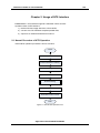
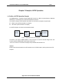
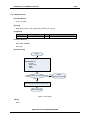
2.1 Normal Procedure of NTS Operation
Normal NTS operation procedure is shown as below.
START
NTS Initialization
External Encoder IC Setting
NTS Configuration
NTS Start
NTS Processing
NTS Reset
External Encoder IC Reset
END
Figure 1-1 Normal NTS Operation Flow
Application Note S19900EJ1V0AN00
CHAPTER 2 USAGE OF NTS INTERFACE
9/26
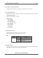
2.2 Detail of Normal NTS Operation Procedure
2.2.1 NTS Initialization
When do NTS initializations, unreset NTS clock by setting ASMU register as below. It’s necessary to
switch the alternate pin to NTS function.
Related register:
RESETREQ0;
RESETREQ0ENA;
AHBCLKCTRL0;
APBCLKCTRL0;
GCLKCTRL2;
GCLKCTRL2ENA;
CHG_PINSEL_G64;
CHG_PINSEL_G80;
CHG_PULL_G08;
Explanation:
GIO P72 ~ P81 are alternated with NTS and other modules.
When switch the alternate pins to NTS function:
bit [31:16] of the register “CHG_PINSEL_G64” are set to “01 01 01 01 01 01 01 01”;
bit [5:0] of the register “CHG_PINSEL_G80” are set to “01 01 01”.
GIO P72 is alternated with NTS_CLK pin.
For NTS clock setting, configure “CHG_PULL_G72” as below:
Signal
Setting
Function
IE
1
Allows input
UPC
0
Not care
POENB
1
Disable Pull-Up/Down
Note:
1. More detail about the CHG registers, please refer to “EMMA Mobile 1 One Chip User’s
Manual”.
2. About the explanation of all the ASMU registers mentioned in this document, please refer to
“EMMA Mobile 1 ASMU/GIO Interface User’s Manual”.
Application Note S19900EJ1V0AN00
CHAPTER 2 USAGE OF NTS INTERFACE
10/26
2.2.2 Configure the External Encoder IC
Configure the external encoder IC according to its’ specification or user’s manual.
2.2.3 Configure NTS module
NTS interface supports PAL mode and NTSC mode. So configure the NTS module according to
the specified output mode;
Set NTS interrupt register as necessary.
Related registers:
NTS_CONTROL;
NTS_FRAMESEL;
NTS_YAREAAD_A/B/C;
NTS_UVAREAAD_A/B/C;
NTS_HOFFSET;
NTS_INTENCLR;
NTS_FFCLR;
NTS_INTENSET;
2.2.4 Start NTS Processing
Start NTS processing by setting NTS_OUT to the not-0 value.
Different setting value performs the different output mode.
Note:
Name
NTS_OUT
Setting
Function
00b
Output OFF (all-0 data is output)
01b
Blackback output
10b
Blueback output
11b
Normal output
2.2.5 NTS Processing
After start the NTS processing, the source data are fetched and converted to the NTS compliant
parallel data. Then output to the external encoder NTSC/PAL IC.
Application Note S19900EJ1V0AN00
CHAPTER 2 USAGE OF NTS INTERFACE
11/26
2.2.6 NTS Reset
Reset NTS interface by setting the related ASMU registers, when exit from NTS function.
Related register:
RESETREQ0;
RESETREQ0ENA;
AHBCLKCTRL0;
APBCLKCTRL0;
GCLKCTRL2;
GCLKCTRL2ENA;
2.2.7 Reset the External Encoder IC
It’s also necessary to reset and power off the external NTSC/PAL encoder IC, when exit from NTS
function.
About the reset operation of the external encoder IC, please refer to its’ specification or user’s
manual.
Application Note S19900EJ1V0AN00
CHAPTER3 SAMPLE OF NTS OPERATION
12/26
Chapter 3 Sample of NTS Operation
3.1 Outline of NTS Operation Sample
On EMMA Mobile 1 evaluation board (PSKCH2Y-S-0016-01), ADV7179 (manufacture: ANALOG
DEVICES) is connected as the external NTSC/PAL encoder IC.
For show the usage of NTS interface with ADV7179, the below 2 samples are performed.
NTSC mode; (NTSC and ADV7179 output)
PAL mode; (PAL and ADV7179 output)
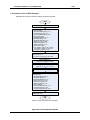
In the NTS samples, the data is transmitted as below:
Memory
YUV422
data
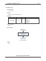
EMMA
Mobile 1
NTS I/F
NTS-compliant
data
ADV7179
TV Monitor
Figure 3-1 Data Flow Chart of NTS Samples
As shown in the figure, EMMA Mobile 1 NTS will fetch the source YUV422 image data, and
convert to NTS compliant data, then output to ADV7179.
1 set of TV monitor is connected to display the processed data via ADV7179.
Caution:
Please make sure all hardware for NTS interface are on READY status, before perform the NTS
samples.
Application Note S19900EJ1V0AN00
CHAPTER3 SAMPLE OF NTS OPERATION
13/26
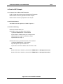
3.2 Operation Flow of NTS Example
Operation flow chart of the NTS sample is shown as below.
START
Prepare source data for NTS sample
NTS Initialization
1] Open clockgate
GCLKCTRL2ENA[24:23] = 11b;
GCLKCTRL2[24:23] = 11b;
GCLKCTRL2ENA[24:23] = 00b;
2] cancel reset device
RESETREQ0ENA[19] = 1b;
RESETREQ0[19] = 1b;
RESETREQ0ENA[19] = 0b;
3] enable auto clock control
AHBCLKCTRL0[24] = 1b;
APBCLKCTRL0[12] = 1b;
4] switch CHG register
CHG_PINSEL_G64[31:16] = 5555H
CHG_PINSEL_G80[5:0] = 010101b
CHG_PULL_G72[2:0] = 101b
External Encoder IC Setting
1] Reset ADV7179
2] Init ADV7179 as NTSC mode output
NTS Configuration
(According the different sample)
NTS Start
[ NTS_OUT = x ] (x = 1, 2 or 3)
NTS Processing
NTS Reset
1] Reset device
RESETREQ0ENA[19] = 1b;
RESETREQ0[19] = 0b;
RESETREQ0ENA[19] = 0b;
2] Disable auto clock control
AHBCLKCTRL0[24] = 0b;
APBCLKCTRL0[12] = 0b;
3] Close clockgate
GCLKCTRL2ENA[24:23] = 11b;
GCLKCTRL2[24:23] = 00b;
GCLKCTRL2ENA[24:23] = 00b;
Release the External Encoder IC
1] Reset ADV7179
END
Figure 3-2 Operation Flow of NTS Sample
Application Note S19900EJ1V0AN00
CHAPTER3 SAMPLE OF NTS OPERATION
14/26
3.3 Detail of NTS Sample
3.3.1 Prepare Source Data for NTS Sample
Load YUV422 data to frame A and frame B for NTS sample.
Data stored in frame A is prepared for NTSC sample;
Data stored in frame B is prepared for PAL sample.
3.3.2 NTS Initialization
Set ASMU and CHG registers, as listed in figure 3-2.
3.3.3 ADV7179 Setting
Reset and Initialize ADV7179.
Reset ADV7179 by call SPI0 driver interface:
1) Initialize EMMA Mobile 1 SPI0 interface
2) Set GPIO10 of PMIC (reset pin) to output mode
3) Make GPIO10 output '0' and wait for stable
4) Make GPIO10 output '1'
Initialize ADV7179 by call SPI0 and I2C driver interface:
1) Initialize EMMA Mobile 1 I2C interface
2) Enable power output for ADV7179
3) Set ADV7179 with the default value of NTSC mode
Note:
Detail of SPI0 driver interface, please refer “EMMA Mobile 1 SPI Application Note”.
Detail of SPI0 driver interface, please refer “EMMA Mobile 1 I2C Application Note”.
Application Note S19900EJ1V0AN00
CHAPTER3 SAMPLE OF NTS OPERATION
15/26
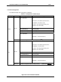
3.3.4 NTS Configuration
For different sample, the configuration is different.
Table 3-1 Configuration of NTS Sample
Sample
Module
Register
NTS_CONTROL
Setting
= 0;
{
UPSCALE = 0b: disable upscale function ;
OUTMODE = 0b: NTSC mode ;
CLKPOL = 0b: rising edge of NTS_CLKI ;
ENDIAN = 0b: Little endian ;
}
NTSC
NTS I/F
NTS_YAREAAD_A
= 0x3100_0000
NTS_UVAREAAD_A
= 0x3110_0000
NTS_HOFFSET
= 720
NTS_FRAMESEL
=1
{
AREASEL = 01b: frame buffer A ;
}
ADV7179
Set ADV7179 registers with NTSC setting values (NOTE), please refer Table 3-2
NTS_CONTROL
= 4;
{
UPSCALE = 0b: disable upscale function ;
OUTMODE = 1b: PAL mode ;
CLKPOL = 0b: rising edge of NTS_CLKI ;
ENDIAN = 0b: Little endian ;
}
PAL
NTS I/F
NTS_YAREAAD_A
= 0x3120_0000
NTS_UVAREAAD_A
= 0x3130_0000
NTS_HOFFSET
= 720
NTS_FRAMESEL
=2
{
AREASEL = 10b: frame buffer B ;
}
ADV7179
Set ADV7179 registers with PAL setting values (NOTE), please refer Table 3-2
Application Note S19900EJ1V0AN00
CHAPTER3 SAMPLE OF NTS OPERATION
16/26
Note:
1. Default setting value sequence of ADV7179 for NTSC/PAL mode are listed in the below
table.
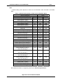
Table 3-2 Default Setting Value of ADV7179 for NTSC/PAL Mode
ADV7179 Register
Mode
Name
Address
NTSC
PAL
Mode Register 0 [MR0]
00
0x00
0x05
Mode Register 1 [MR1]
01
0x10
0x10
Mode Register 2 [MR2]
02
0x00
0x00
Mode Register 3 [MR3]
03
0x00
0x00
Mode Register 4 [MR4]
04
0x10
0x00
Reserved
05
0x00
0x00
Reserved
06
0x00
0x00
Timing Mode Register 0 [TR0]
07
0x00
0x00
Timing Mode Register 1 [TR1]
08
0x00
0x00
Subcarrier Freq Reg 0
09
0x1E
0xCB
Subcarrier Freq Reg 1
0A
0x7C
0x8A
Subcarrier Freq Reg 2
0B
0xF0
0x09
Subcarrier Freq Reg 3
0C
0x21
0x2A
Subcarrier Phase Reg
0D
0x00
0x00
Closed Captioning Ext Data Byte 0
0E
0x00
0x00
Closed Captioning Ext Data Byte 1
0F
0x00
0x00
Closed Captioning Data Byte 0
10
0x00
0x00
Closed Captioning Data Byte 1
11
0x00
0x00
NTSC Pedestal Ctrl Reg 0 /
12
0x00
0x00
13
0x00
0x00
14
0x00
0x00
15
0x00
0x00
CGMS_WSS_0 [C/W0]
16
0x00
0x00
CGMS_WSS_1 [C/W1]
17
0x00
0x00
CGMS_WSS_2 [C/W2]
18
0x00
0x00
TeleText Request Ctrl Reg [TC07]
19
0x00
0x00
PAL TTX Ctrl Reg 0
NTSC Pedestal Ctrl Reg 1 /
PAL TTX Ctrl Reg 1
NTSC Pedestal Ctrl Reg 2 /
PAL TTX Ctrl Reg 2
NTSC Pedestal Ctrl Reg 3 /
PAL TTX Ctrl Reg 3
More detail about ADV7179 registers, please refer “ADV7179 Specification”.
Application Note S19900EJ1V0AN00
CHAPTER3 SAMPLE OF NTS OPERATION
17/26
3.3.5 Start NTS Processing
Start NTS processing by setting “NTS_OUT” with not-0 value.
For NTSC and PAL sample, set the register to “3”; it is normal output mode.
3.3.6 NTS Processing
After start the NTS processing, the source data are fetched and converted to the NTS compliant
parallel data. Then output to ADV7179. It will be displayed in the connected TV monitor finally.
3.3.7 NTS Reset
After complete NTS NTSC and PAL function evaluation, reset NTS interface by setting ASMU
registers as listed in figure 3-2.
3.3.8 Release ADV7179
Reset and power off ADV7179 as the below sequence.
1) Initialize SPI0
2) Set GPIO10 of PMIC (reset pin) to output mode
3) Make GPIO10 output '0'
Application Note S19900EJ1V0AN00
CHAPTER3 SAMPLE OF NTS OPERATION
18/26
3.4 ADV7179 Color Bar Function
As additional, ADV7179 color bar function is evaluated as an individual sample.
It will generate and output an internal color bar test pattern. It is important to note that when color
bars are enabled, the ADV7179 is configured in a master timing mode.
Under this sample, ADV7179 is used only. So the operations of NTS are unnecessary.
Operation of this sample is as below:
1) ADV7179 Setting
Same with “3.3.3 ADV7179 Setting”
2) Set ADV7179 to color bar mode
Set bit[7] of ADV7179 Mode Register 1 with “1”, to enable color bar function.
3) Check the color bar pattern displayed in TV monitor
4) Reset and power off ADV7179
Same with “3.3.8 Release ADV7179”.
Application Note S19900EJ1V0AN00
APPENDIX A. NTS DRIVER FUNCTION
19/26
Appendix A. NTS Driver Function
A.1 NTS API function list
The following table shows the NTS interface functions:
Table A-1 NTS Driver Function List
Type
Driver
Function
Function Name
em1_nts_init
em1_nts_release
em1_nts_setup
em1_nts_start
em1_nts_irq_enable
em1_nts_irq_handle
Function Detail
Initialize NTS interface
Release NTS interface
Configure NTS interface
Start NTS processing
Enable NTS Interrupt
NTS Interrupt handler
A.2 Type Define
A.2.1 Naming rule and coding rule
About naming rule and coding rule, please refer to “GD_SPEC_EM1_AN&TP.pdf”
A.2.2 Structure
Table A-2 Structure Define
Structure Name
NTS_SETUP_ST
Structure Member
uchar upscale
uchar outmode
uint clkpol
uint endian
uint buffer_a_y
uint buffer_b_y
uint buffer_c_y
uint buffer_a_uv
uint buffer_b_uv
uint buffer_c_uv
uint hoffset
uint frame_sel
Application Note S19900EJ1V0AN00
APPENDIX A. NTS DRIVER FUNCTION
20/26
A.3 Function Detail
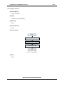
A.3.1 Initialization Function
[Function Name]
em1_nts_init
[Format]
void em1_nts_init(void);
[Argument]
None
[Function Return]
None
[Function Flow]
START
Open Gateclock for NTS
Enable NTS auto clock control
Unreset NTS
Switch CHG to NTS
END
Figure A-1 NTS Initialization
[Note]
None
Application Note S19900EJ1V0AN00
APPENDIX A. NTS DRIVER FUNCTION
21/26
A.3.2 Release Function
[Function Name]
em1_nts_release
[Format]
void em1_nts_release(void);
[Argument]
None
[Function Return]
None
[Function Flow]
START
Reset NTS
Dsiable NTS auto clock control
Close NTS Gateclock
END
Figure A-2 NTS Release
[Note]
None
Application Note S19900EJ1V0AN00
APPENDIX A. NTS DRIVER FUNCTION
22/26
A.3.3 Setup Function
[Function Name]
em1_nts_setup
[Format]
DRV_RESULT em1_nts_setup (NTS_SETUP_ST* nts_st);
[Argument]
Parameter
Type
I/O
nts_st
NTS_SETUP_ST *
I
Detail
All necessary setting for NTS
[Function Return]
DRV_ERR_PARAM;
DRV_OK;
[Function Flow]
START
Check the register setting value
[Check Items] = {
upscale;
output mode;
clkpol;
endian;
}
All setting values are OK?
No
Return
DRV_ERR_PARAM
Yes
Set NTS Register with the input values
Return DRV_OK
Figure A-3 NTS Setup
[Note]
None
Application Note S19900EJ1V0AN00
APPENDIX A. NTS DRIVER FUNCTION
23/26
A.3.4 Start Function
[Function Name]
em1_nts_start
[Format]
void em1_nts_start(uint display_mode);
[Argument]
Parameter
display_mode
Type
uint
I/O
I
Detail
output mode :
OFF;
Blackback;
Blueback;
Normal;
[Function Return]
None
[Function Flow]
START
Start NTS Processing
[ NTS_OUT = x ]
(x = 1, 2, or 3)
END
Figure A-4 NTS Start
[Note]
None
Application Note S19900EJ1V0AN00
APPENDIX A. NTS DRIVER FUNCTION
A.3.5 INT Enable Function
[Function Name]
em1_nts_irq_enable
[Format]
void em1_nts_irq_enable(void);
[Argument]
None
[Function Return]
None
[Function Flow]
None
[Note]
None
Application Note S19900EJ1V0AN00
24/26
APPENDIX A. NTS DRIVER FUNCTION
A.3.6 INT Handler Function
[Function Name]
em1_nts_irq_handle
[Format]
void em1_nts_irq_handle(void);
[Argument]
None
[Function Return]
None
[Function Flow]
None
[Note]
None
Application Note S19900EJ1V0AN00
25/26
ANNEX MODIFICATION HISTORY
26/26
ANNEX Modification History
Number
Ver 1.00
Modification Contents
Author
New version
Application Note S19900EJ1V0AN00
Date
Aug,4, 2009