1
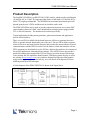
FastPMC Products
FastPMC-DFLEX64
TTL/EIA-485 I/O Module
User’s Manual RevC
TEK/TM-322C
March 2002
FPMC-DFLEX64 User’s Manual
TEK Microsystems has made every effort to ensure that this manual is accurate and complete.
However, TEK reserves the right to make changes and improvements to the products described
in this manual at any time and without notice.
This product is covered by a limited warranty which is described in the manual. Other than the
stated limited warranty, TEK disclaims all other warranties, including the warranties of
merchantability and of fitness for a particular purpose. In the event of a failure of the hardware
or software described in this manual, TEK’s obligation is limited to repair or replacement of the
defective item, or, if the item cannot be repaired or replaced, a refund of the purchase price for
the item. TEK assumes no liability arising out of the application or use of the hardware or
software, and assumes no responsibility for direct, indirect, incidental or consequential damages
of any kind.
The electronic equipment described in this manual generates, uses, and can radiate radio
frequency energy. Operation of this equipment in a residential area is likely to cause radio
interference, in which case the user, at his own expense, will be required to take whatever
measures may be required to correct the interference.
TEK Microsystems’ products are not authorized for use as critical components in life support
devices or systems without the express written agreement of an officer of TEK Microsystems.
This manual is Copyright © 2001 TEK Microsystems, Incorporated. All Rights Reserved.
FastPMC is a trademark of TEK Microsystems, Incorporated.
Other trademarks and registered trademarks used are owned by their respective manufacturers.
Revision Information:
This manual describes hardware revision “A” of the FPMC-DFLEX64.
Document ordering code and release information:
URL: http://www.tekmicro.com/tm322.revC.pdf
TEK/TM-322C
March 2002
Page i
FPMC-DFLEX64 User’s Manual
Table of Contents
Product Description ......................................................................................................1
Specifications ................................................................................................................2
Support Information ......................................................................................................3
Warranty Information................................................................................................................ 3
Contact Information .................................................................................................................. 3
Additional Documentation........................................................................................................ 4
Installation and Setup ...................................................................................................5
Overview ................................................................................................................................... 5
Unpacking and Handling........................................................................................................... 5
Installation................................................................................................................................. 6
Software Download and Installation......................................................................................... 7
Theory of Operation ......................................................................................................8
Overview ................................................................................................................................... 8
PCI Interface ............................................................................................................................. 8
Local Bus .................................................................................................................................. 9
Buffer Memory.......................................................................................................................... 9
Serial EEPROM ...................................................................................................................... 10
Customizable FPGA................................................................................................................ 11
Clock Architecture .................................................................................................................. 12
EIA-485 Transceivers ............................................................................................................. 13
Switching Network.................................................................................................................. 13
Modes of Operation ................................................................................................................ 13
Connector Interface................................................................................................................. 14
Software Interface .......................................................................................................15
Overview ................................................................................................................................. 15
Initialization ............................................................................................................................ 16
Initialization: Serial EEPROM Load................................................................................ 16
Initialization: PCI Address Configuration........................................................................ 19
Initialization: Read Serial EEPROM................................................................................ 19
Initialization: Download FPGA Program ......................................................................... 20
Initialization: Clock Synthesizer ...................................................................................... 21
Configuration Space................................................................................................................ 22
I/O and Memory Space: PCI 9080 Registers .......................................................................... 22
PCI 9080 PCI Configuration Registers............................................................................. 23
PCI 9080 Local Configuration Registers.......................................................................... 23
PCI 9080 Runtime Registers ............................................................................................ 26
PCI 9080 DMA Registers................................................................................................. 27
PCI 9080 Messaging Queue Registers ............................................................................. 28
Memory Space: FPGA Registers ............................................................................................ 28
Interrupts ................................................................................................................................. 28
BUSMODE Signals ................................................................................................................ 28
DMA Requests ........................................................................................................................ 28
Page ii
FPMC-DFLEX64 User’s Manual
Product Description
The FastPMC DFLEX64 is an IEEE P1386.1 PMC module, which provides a full-duplex
(16-bit EIA-485 or 32 bit TTL) high-speed data link or a half-duplex (32-bit EIA-485 or
64 bit TTL) high-speed data link. The DFLEX64 bus maximum operational speed will
depend upon the user’s FPGA and the mode in which the card is used.
The FPMC-DFLEX64 may be used to provide connectivity between two or more PMC
carrier boards or between a PMC carrier board and an external system equipped with a
TTL or EIA-485 interface. The board must be ordered specifically.
Typical applications include pattern generators, pulse measurements and applicationspecific serial interfaces.
There is a test FPGA available for the board but users will have to generate their own
FPGA to get their desired functionality out of the card. The test FPGA defines registers
which will write to and read from the data pins and provides the state machines for serial
communications with the EPLD in order to set the mode in which the hardware will run.
FPGA programs are downloaded over the PCI bus, allowing the module to be customized
for specific applications without hardware changes. The test FPGA does not provide a
means for bursting data on and off the PCI bus as this was not the intent of this design.
Users desiring fast I/O capabilities should contact TEK Microsystems directly or access
the website at www.tekmicro.com to view products designed for high-speed data transfer
using similar logic interfaces. Alternatively, users can decide to incorporate PCI data
buffering inside their FPGA designs.
A block diagram of the FPMC-DFLEX64 is shown in the figure below.
Page 1
FPMC-DFLEX64 User’s Manual
Specifications
I/O Interface
32 EIA-485 I/O pairs or
64 TTL I/O signals
Clock Rate
DC to X MHz (where X is dependent primarily on the
user’s FPGA)
PCI Bus Interface
PCI 2.1 compatible, 32 bit, 33 MHz
Compatible with 3.3V or 5V signal levels
PCI Throughput
132 MB/s burst
Supports zero wait state memory accesses
FPGA Logic Capacity
Altera EPF10K50VRC240-3, 36K to 116K gates
(Optional EPF10K100VRC240-3, or –1 devices
available)
Memory Capacity
1 MB, organized as 256K x 32
Memory function is determined by FPGA program
Interrupts
Programmable through FPGA
DMA
Two integrated linked-list DMA controllers
Power Requirements
+5 Volts, 700mA typical
Operating Temperature
0 to 70 degrees C.
Storage Temperature
-40 to +85 degrees C.
Page 2
FPMC-DFLEX64 User’s Manual
Support Information
Warranty Information
The FPMC-DFLEX64 is warranted against defects in material or workmanship for a
period of one year from the original date of purchase. If a failure occurs within the
warranty period, TEK will repair or replace the product at no cost to the user. For
warranty repair, please contact TEK as described below and obtain an RMA number and
return shipping instructions.
Contact Information
If technical support or repair assistance is required, please contact TEK through one of
the following methods:
Internet
http://www.tekmicro.com/
Email
mailto:[email protected]
Telephone
+1 781 270 0808
Facsimile
+1 781 270 0813
Mail
TEK Microsystems, Incorporated
One North Avenue
Burlington, MA 01803-3313
Page 3
FPMC-DFLEX64 User’s Manual
Additional Documentation
The FPMC-DFLEX64 module uses off-the-shelf components to implement several key
functions, including the PCI bus interface, Serial EEPROM, and the EIA-485 transceiver.
Review of the following additional documentation may be useful for proper operation and
control of the FPMC-DFLEX64.
•
PLX Technologies PCI 9080 Data Book
Web site: http://www.plxtech.com/
URL: Requires registration with PLX Technologies
•
Fairchild (formerly National) NM93CS46 Serial EEPROM
Web site: http://www.fairchildsemi.com/
URL: http://www.fairchildsemi.com/ds/FM/FM93CS46.pdf
•
Texas Instruments EIA-485 Transceiver
Web site: http://www.fairchildsemi.com/
URL: http://www-s.ti.com/sc/psheets/slls218b/slls218b.pdf
•
Cypress ICD2053 PLL Clock Synthesizer
Web site: http://www.cypress.com/
URL: http://www.cypress.com/pub/datasheets/icd2053b.pdf
•
Altera Application Note AN116, Configuring FLEX 10K Devices
Web site: http://www.altera.com/
URL: http://www.altera.com/literature/an/an116.pdf
•
Altera Classic EPLD Family Data Sheet
Web site: http://www.altera.com/
URL: http://www.altera.com/literature/ds/classic.pdf
The PDF or HTML versions of these data sheets may be accessed through the
manufacturers’ web pages as shown above. The URLs were valid as of the date of this
manual.
Printed versions of the above data sheets are available from TEK’s technical support
department.
Page 4
FPMC-DFLEX64 User’s Manual
Installation and Setup
Overview
The FPMC-DFLEX64 is a standard 74mm x 149mm PCI Mezzanine Card (PMC) which
occupies a single slot in the host module. The installation and setup procedure consists of
several steps:
1. Unpacking and inspecting the card.
2. Installation of the FPMC-DFLEX64 into the Host module.
3. Downloading and installing the appropriate software driver for the FPMC-DFLEX64.
Each of these steps is described in more detail in the sections below.
Unpacking and Handling
The FPMC-DFLEX64 is shipped inside an ESD-safe container.
The FPMC-DFLEX4 package should contain the following items upon unpacking:
•
FPMC-DFLEX64 card.
•
Electromagnetic Interference (EMI) Gasket
•
Rev C User Manual
The FPMC-DFLEX64 contains electronic circuits that are susceptible to damage through
mishandling or through application of electrostatic discharge (ESD). The following
precautions should be observed when unpacking, installing, or using an FPMC-DFLEX64
card.
•
Whenever the FPMC-DFLEX64 is being handled outside of an ESD-safe shipping
container, the user should maintain ESD-safe conditions through usage of a grounding
wrist strap or other such static preventive measures.
•
The FPMC-DFLEX64 should never be installed or removed from the slot when
power is being applied to the system or applied directly to the card.
•
The FPMC-DFLEX64 should never be forced into the slot during installation.
Insertion of the card into should require only moderate “hand pressure”. If more
pressure is required for the insertion the card should be removed and the connectors
examined to determine the source of the problem.
Like any other electronic circuit card, the FPMC-DFLEX64 will provide years of reliable
operation if handled in accordance with these guidelines.
Page 5
FPMC-DFLEX64 User’s Manual
Installation
The front panel view of the FPMC-DFLEX64 card along with a host module and
DFLEX64 cable is shown below (subject to change):
HOST
MODULE
FPMC-DFLEX64
Connecting Point
Connector
Connector
Connector
Connector
80 Pin Connector
..
..
..
..
..
..
..
..
..
..
..
..
..
..
..
..
..
..
..
SCSI-68 CABLE
Connecting
Point
Slot
Opening
The FPMC-DFLEX64 card displayed here demonstrates the DFLEX64 interface on the
front panel of the card. To install the FPMC-DFLEX64 card into a host machine, the
card must be kept upright with the three PMC connectors on the board matching up with
the PMC connectors on the carrier. Standard SCSI (Small Computer Systems Interface)
68 pin connectors are used for the FPMC-DFLEX64 front panel connector, the pinout for
which is discussed in the Connector Interface section of this manual. The EMI gasket is
to be wrapped around the bezel of the FPMC-DFLEX64 before insertion into the host
module. The card should be inserted into the host by first fitting the bezel into the front
panel of the host and then lining up the connectors and applying minimal pressure to the
area of the card above the PMC connectors (labeled “Connector” in the above diagram).
Page 6
FPMC-DFLEX64 User’s Manual
Software Download and Installation
The software driver and demonstration programs can be downloaded off the Products
section of the TEK Microsystems homepage located at:
http://www.tekmicro.com
The driver distribution is in the TAR.GZ format and contains all required source and
include files.
To install the files on a Solaris system, enter the following commands:
gunzip dflex64.current.tar.gz
tar xvf dflex64.current.tar
This will create the required directories and place all the required files in those
directories.
Running the command “make” in this directory will create the driver object files along
with a suite of demonstration programs.
The FPMC-DFLEX64 still requires several initialization procedures before the card can
be used, which the drivers are designed to perform. These procedures are described in
detail in the Software Initialization section of this manual.
After initialization, the Manufacturing tests can be run to verify the installation (Note the loop test will fail because it requires a loop back cable which is not provided).
Page 7
FPMC-DFLEX64 User’s Manual
Theory of Operation
Overview
The FPMC-DFLEX64 provides a high-speed customizable interface between a PCI/PMC
host system and an external system using either TTL or EIA-485 logic levels. The card
must be ordered to run in either EIA-485 only mode or in TTL only mode. This is a
factory configuration option and is not recommended as an option for users to attempt. A
block diagram of the FPMC-DFLEX64 is shown below.
The operation of each of the hardware subsystems is discussed below.
PCI Interface
The PCI/PMC interface is implemented using an off-the-shelf PCI 9080 interface
controller from PLX Technologies. The PCI 9080 implements all necessary PCI bus
interface functions, including configuration space, EEPROM interface, PCI interrupter for
local interrupts, and two linked-list DMA controllers.
The PCI bus interface is compliant with the PCI 2.1 specification and operates at 33 MHz
with a 32-bit data bus. The FPMC-DFLEX64 is compatible with 3.3V and 5V PCI signal
levels.
Many of the features of the FPMC-DFLEX64 are implemented through the local bus
interface using PCI 9080 resources. For example, the FPMC-DFLEX64 bus-mastering
DMA capability is implemented using the PCI 9080 DMA controllers. To reach a
complete understanding of how to use the FPMC-DFLEX64 features, the user is strongly
encouraged to review the PCI 9080 data book along with this manual.
The data book for the PCI 9080 is available on PLX Technologies web site:
(http://www.plxtech.com) and is also available on request from TEK’s technical support
department.
Page 8
FPMC-DFLEX64 User’s Manual
Local Bus
The FPMC-DFLEX64 has an internal local bus that is used to communicate between the
PCI 9080, the FPGA and the buffer memory. The local bus implements a 32-bit
multiplexed address/data bus and associated control signals.
The local bus is arbitrated between the PCI 9080 and the FPGA. The PCI 9080 acts as
the bus master to implement transactions between the PCI bus and the FPGA and also to
implement DMA transactions between the PCI 9080 internal FIFOs and the FPGA.
The local bus also implements two DMA request/acknowledge signals and a local
interrupt, which may be used to generate PCI interrupts through the PCI 9080.
The local bus protocol is completely defined in the PCI 9080 data book. The FPMCDFLEX64 uses the PCI 9080 “J” bus mode.
Buffer Memory
The FPMC-DFLEX64 has a static RAM buffer memory. The buffer memory is
implemented using two CY7C1041-17ZC 256K x 16 static RAM IC’s. The memory
implementation has additional logic to gate the write control signal from the FPGA,
allowing the memory subsystem to sustain local bus bursts of single clock read and write
cycles.
A block diagram of the buffer memory implementation is shown below.
CONTROL SIGNALS
CONTROL SIGNALS
PCI 9080
FPGA
MEMORY ADDRESS
BUFFER
MEMORY
LOCAL ADDRESS/DATA
Local bus transactions may be generated by the PCI 9080 or by the FPGA. The PCI 9080
will generate local bus transactions when requested by the PCI bus (i.e. when acting as a
PCI Target) or when driven by the PCI 9080 internal DMA controllers.
Page 9
FPMC-DFLEX64 User’s Manual
The standard FPGA programs use the LA[22] bit to determine whether a local bus cycle
accesses control/status registers (LA[22] low) or the FIFO memory (LA[22] high). Note
however that FIFO accesses are not implemented in the test FPGA supplied with this
design. With the default configuration of the PCI 9080, the address range defined by
BAR2 has the LA[22] bit forced low and the address range defined by BAR3 has the
LA[22] bit forced high. Therefore, all accesses to the BAR2 region will access
control/status registers and all accesses to the BAR3 region will access the FIFO memory
(if implemented by the user).
Because the LA[21..2] address bits are ignored during FIFO accesses, the BAR3 memory
region can be of arbitrary size, depending only on the operating environment’s
constraints. TEK’s default configuration defines a 4-MB memory region to support the
possibility of large DMA transfers using an external DMA controller that requires
incrementing the PCI address. If all DMA transfers are performed using the PCI 9080
DMA controllers, the BAR3 memory region can be configured for a smaller size as the
PCI 9080 DMA controller has a fixed vs. incrementing local address option (controlled
through DMAMODE bit 11).
Because the buffer memory address and control signals are controlled by the FPGA,
alternate memory implementations are possible through FPGA reprogramming.
Specifically, implementations that perform random accesses to memory (i.e. quadrant-toraster conversion of incoming frame data or similar functions) are quite feasible, as are
implementations that simply map the buffer memory into linear PCI address space
without FIFO semantics.
Serial EEPROM
The PCI 9080 interface controller has a built-in interface to a serial EEPROM device.
The serial EEPROM is used as a source for PCI 9080 configuration information after PCI
reset and as a resource for the user to store non-volatile configuration information about
the PCI/PMC card.
In the FPMC-DFLEX64, the serial EEPROM interface is connected to a Fairchild
NM93CS46 (or similar part) 1,024-bit serial EEPROM organized as 64 sixteen-bit words.
The first 44 words (88 bytes) of the EEPROM are used to define the PCI 9080
configuration registers. The next 11 words are available for user data and the last 9 words
are used for FPMC-DFLEX64 configuration information.
The PCI 9080 Serial EEPROM interface signals are also used to download FPGA
program information to the FPGA device.
The data sheet for the NM93CS46 is available on Fairchild’s web site
(http://www.fairchildsemi.com) and is also available on request from TEK’s technical
support department.
Page 10
FPMC-DFLEX64 User’s Manual
Customizable FPGA
The FPMC-DFLEX64 implements most of the onboard logic using an in-systemprogrammable FPGA device. The standard FPGA device is an Altera
EPF10K50VRC240-3, which provides between 36,000 and 116,000 gates of logic
capability along with 20,480 bits of internal RAM memory (or an optional device as
discussed earlier under the Specification heading of this document).
The FPGA program is downloaded through the PCI bus using the user I/O and serial
EEPROM signals from the PCI 9080. The local bus is inoperative prior to FPGA
download as the local bus acknowledge signals are always inactive until driven by the
FPGA.
The FPGA functionality and memory space registers are described in the FPGA
documentation for the test FPGA.
Page 11
FPMC-DFLEX64 User’s Manual
Clock Architecture
A diagram showing the clock architecture of the FPMC-DFLEX64 is shown below.
PCI
CLK
LCLK
BPCLKo
BPCLKo
EPLD
Div. by 2
CLOCK
SYNTHESIZERS
XTAL
CLK
CYPRESS ICD2053
SCLKA &
SCLKB
CONTROL
LCLK
FPGA
XTAL
HCLK
PCI 9080
CLOCK DRIVER
LCLK
49fCT805A
LCLK
LCLK
1 MB
BUFFER
MEMORY
The details of the internal FPMC-DFLEX64 clock domains are primarily of interest to
users who are developing their own FPGA programs. The clock routing operates as
follows:
•
First, the PCI bus and the PCI interface portion of the PCI 9080 are synchronous to
the PCI bus clock. The clock domain is not shown in the diagram above, as it does
not interact with the rest of the card.
•
The PCI 9080 generates a clock output, which is a regenerated version of the PCI bus
clock. This signal is named BPCLKo.
•
The sythesizer reference clock is a version of either BPCLKo or a 33.33 MHz crystal
oscillator output divided by 2. The crystal is most useful for users operating in
environments with unsuitable PCI clocks (as is the case in many personal computers).
The divide by 2 is required because the ICD2053 is limited to a maximum reference
clock frequency of 25 MHz. One of the ICD2053 clock synthesizers is used as the
source of LCLK. All local bus activity is synchronous to the LCLK signal. The other
ICD2053 is used to generate HCLK (link clock). Both clocks can be used as the
timing source for the FPGA.
The clock synthesizers have no hardware reset signal. Therefore, the clock synthesizers
should be considered to be in an indeterminate state after FPGA download or PCI bus
reset.
Page 12
FPMC-DFLEX64 User’s Manual
EIA-485 Transceivers
The FPMC-DFLEX64 implements data transfer in and out of the module with Texas
Instruments SN75976 EIA-485 transceivers when in a mode that uses EIA-485 logic
levels. Each transceiver carries 8 bits of data.
Switching Network
When in a mode that requires TTL logic levels for data transfers across the front panel
connector, switches are used to have the data pins of the FPGA connected to the pins on
the SCSI connector through the switching network. The result is the connection of the
FPGA I/O pins to the front panel connector.
Modes of Operation
The FPMC-DFLEX64 is set up to have user-defined settings for each I/O block. For our
purposes, a block is defined as a group of 8 EIA-485 signal pairs or 16 TTL signal lines.
The card consists of 4 independent blocks that can be set for inputs or outputs in either
TTL or EIA-485 mode. Blocks can be set up in any direction (input or output) desired by
the user as long as the entire block remains consistent. The entire block must be
operating in the same direction for EIA-485 mode. Logic levels cannot be mixed within a
FPMC-DFLEX board (this is not a supported use for this card). The entire board will
communicate with either EIA-485 logic levels or with TTL logic levels.
Page 13
FPMC-DFLEX64 User’s Manual
Connector Interface
The FPMC-DFLEX64 Rev A J1 connector pinout is shown in the table below:
BLOCK
1
1
1
1
1
1
1
1
1
1
1
1
1
1
1
1
2
2
2
2
2
2
2
2
2
2
2
2
2
2
2
2
LABEL
A0
B0
A1
B1
A2
B2
A3
B3
A4
B4
A5
B5
A6
B6
A7
B7
A8
B8
A9
B9
A10
B10
A11
B11
A12
B12
A13
B13
A14
B14
A15
B15
PIN
1
35
2
36
3
37
4
38
5
39
6
40
7
41
8
42
9
43
10
44
11
45
12
46
13
47
14
48
15
49
16
50
BLOCK
3
3
3
3
3
3
3
3
3
3
3
3
3
3
3
3
4
4
4
4
4
4
4
4
4
4
4
4
4
4
4
4
LABEL
A16
B16
A17
B17
A18
B18
A19
B19
A20
B20
A21
B21
A22
B22
A23
B23
A24
B24
A25
B25
A26
B26
A27
B27
A28
B28
A29
B29
A30
B30
A31
B31
PIN
17
51
18
52
19
53
20
54
21
55
22
56
23
57
24
58
25
59
26
60
27
61
28
62
29
63
30
64
31
65
32
66
LABEL
GND
GND
RSVD
RSVD
PIN
33
67
34
68
Page 14
FPMC-DFLEX64 User’s Manual
Software Interface
Overview
The software interface to the FPMC-DFLEX64 is implemented using the PCI/PMC bus.
The FPMC-DFLEX64 uses the PLX Technologies PCI 9080 controller to implement the
PCI/PMC bus interface. The PCI 9080 provides the logic required to support operation as
both a PCI Master (used for bus-mastering DMA transfers between the FPMC-DFLEX64
and the host memory) and a PCI Target (used for access to control/status registers in the
PCI 9080 and the FPMC-DFLEX64 FPGA).
The PCI 9080 is typically configured with four separate PCI address spaces.
•
The first address space, programmed through the PCI configuration space BAR0
register, defines a PCI memory space which is mapped to the PCI 9080 control
registers.
•
The second address space, programmed through the PCI configuration space BAR1
register, defines a PCI I/O space which is also mapped to the PCI 9080 control
registers.
•
The third address space, programmed through the PCI configuration space BAR2
register, defines a PCI memory space which is mapped to the FPMC-DFLEX64 local
bus with LA[22] low. This address space is used for access to the FPGA
control/status registers.
•
The fourth address space, programmed through the PCI configuration space BAR3
register, defines a PCI memory space which is mapped to the FPMC-DFLEX64 local
bus with LA[22] high. This address space can be used for access to the buffer
memory FIFOs.
In the test FPGA, the various I/O registers are used to configure the operating mode to set
the logic levels on the pins for loopback testing purposes.
Each time the FPMC-DFLEX64 is powered up, the board must be initialized, first with
the PCI configuration information and then with the FPGA program image. The
initialization sequences are described in the following pages.
Page 15
FPMC-DFLEX64 User’s Manual
Initialization
The FPMC-DFLEX64 requires several steps of initialization before the card can be used
in a system. The initialization steps are:
•
Load the PCI 9080 control registers from Serial EEPROM. This function is
performed automatically by the PCI 9080 whenever the PCI bus is reset.
•
Configure the Base Address Registers in the PCI configuration space. This is
typically performed by the PCI/PMC host carrier BIOS or other startup code running
on the host processor.
•
Read the Serial EEPROM configuration information to determine the type of FPGA
device installed on the FPMC-DFLEX64.
•
Download the desired FPGA program image to the FPMC-DFLEX64.
•
If required, configure the ICD2053 clock synthesizers.
Each of these steps is described below.
Initialization: Serial EEPROM Load
The PCI 9080 is initially configured using a serial EEPROM device on the FPMCDFLEX64. The serial EEPROM device is a Fairchild NM93CS46 (or similar device)
1,024-bit EEPROM organized as 64 sixteen-bit words. The serial EEPROM is used as
the source for an “Extra Long Serial EEPROM Load” as described in sections 3.3.2 and
3.3.3 of the PCI 9080 Data Book. The table below lists the EEPROM locations and their
functions.
For each EEPROM word, the table shows the Serial EEPROM byte offset of the word,
PCI 9080 register name, address space, offset, and programmed value. Registers listed as
“CFG” are in the PCI configuration space and registers listed as “REG” are accessible
through the BAR0/BAR1 address spaces.
Many of the following registers have recommended values based on the implementation
of both the FPMC-DFLEX64 local bus and of the standard FPGA programs available
from TEK. If the user develops a custom FPGA program, it may be necessary to modify
some of the local bus control registers to match the user’s FPGA implementation.
Offset
PCI 9080 Register
Value
Comments
0
CFG 0x02: Device ID
0x2920
Specifies FPMC-DFLEX64
model
2
CFG 0x00: Vendor ID
0x14CF
TEK Microsystems’ Vendor ID
4
CFG 0x0A: Class Code
0x0E00
6
CFG 0x08: Class Code/Rev
0x0001
8
CFG 0x3E: Maximum Latency,
Minimum Grant
0x0008
Page 16
FPMC-DFLEX64 User’s Manual
Offset
10
PCI 9080 Register
Value
Comments
CFG 0x3C: Interrupt Pin, Interrupt
Line Routing
0x0100
INTA pin used by FPMCDFLEX64
12/14
REG 0x40: MBOX0
Mailbox 0
0x00000000
Not used
16/18
REG 0x44: MBOX1
Mailbox 1
0x00000000
Not used
20/22
REG 0x00: LAS0RR
Range for PCI-to-Local Address
Space 0
0xFFFF0000
64 KB memory address
space for local space 0
(BAR2)
24/26
REG 0x04: LAS0BA
Local Base Address (Remap) for PCIto-Local Address Space 0
0x00000001
The remapped A[22] bit must
be low for proper operation
with the standard FPGA
program.
28/30
REG 0x08: MARBR
Local Arbitration Register
0x11E00000
Local bus operating modes
must match FPGA program.
32/34
REG 0x0C: BIGEND
Local Bus Big/Little Endian Descriptor
Register
0x00000000
Specifies little endian mode
for all accesses.
36/38
REG 0x10: EROMRR
Range for PCI-to-Local Expansion
ROM
0xFFF00000
Not used
40/42
REG 0x14: EROMBA
Local Base Address (Remap) for PCIto-Local Expansion ROM
0x10000010
Not used
44/46
REG 0x18: LBRD0
Bus Region Descriptors for PCI-toLocal Accesses
0x4F0305C3
Local bus operating
parameters must match
FPGA program.
48/50
REG 0x1C: DMRR
Range for Direct Master to PCI
0xFF000000
Not used
52/54
REG 0x20: DMLBAM
Local Base Address for Direct Master
to PCI Memory
0x40000000
Not used
56/58
REG 0x24: DMLBAI
Local Bus Address for Direct Master
to PCI IO/Cfg
0x70000000
Not used
60/62
REG 0x28: DMPBAM
PCI Base Address (Remap) for Direct
Master to PCI
0x0000183F
Specifies Direct Master
operating parameters.
64/66
REG 0x2C: DMCFGA
PCI Configuration Address Register
for Direct Master to PCI IO/Cfg
0x00000000
Not used
68
CFG 0x2E: Subsystem ID
0x3221
Specifies FPMC-DFLEX64
model
70
CFG 0x2C: Subsystem Vendor ID
0x14CF
TEK Microsystems’ Vendor ID
Page 17
FPMC-DFLEX64 User’s Manual
Offset
PCI 9080 Register
Value
Comments
72/74
REG 0xF0: LAS1RR
Range for PCI-to-Local Address
Space 1
0xFFC00000
4 MB memory address space
for local space 1 (BAR3)
76/78
REG 0xF4: LAS1BA
Local Base Address (Remap) for PCIto-Local Address Space 1
0x00400001
The remapped A[22] bit must
be high for proper operation
with the standard FPGA
program.
80/82
REG 0xF8: LBRD1
Bus Region Descriptors (Space 1) for
PCI-to-Local Accesses
0x000003C3
Local bus operating
parameters must match
FPGA program.
84/86
CFG 0x30: PCI Base Address for
Local Expansion ROM
0x00000000
Not used
The first 88 bytes of the 128-byte serial EEPROM are used by the PCI 9080 as shown
above. Bytes 88 through 103 are available for user programming. Bytes 104 through 127
are programmed at the factory as follows:
Offset
Register
Typical
Value
Comments
104
Back end Model number
0x2920
FPMC-DFLEX64 model number
106
Back end MSW of serial
number
0x292
FPMC-DFLEX64 serial number
(decimal)
108
Back end LSW of serial
number
0x0001
110
Model Number
0x3221
FPMC-DFLEX64 model number
112
MSW of serial number
0x322
FPMC-DFLEX64 serial number
(decimal)
114
LSW of serial number
0x0001
116
Hardware revision level
1
FPMC-DFLEX64 hardware revision
118
Memory Size (KB)
0 or 1024
FPMC-DFLEX64 installed memory
FPGA Device
0x1323
Installed FPGA device, divided into
three fields. The 0xF000 portion is
the FPGA family (0 = FLEX10K, 1 =
10KV, 2 = 10KA, 3 = 10KE). The
0x0FF0 portion is the device size (30
= 10K30, 50 = 10K50). The 0x000F
portion is the device speed (1 = “-1”, 2
= “-2”, 3 = “-3”).
122
External I/O Interfaces
0x0100
124
Reserved
0
Reserved for future use
126
Reserved
0
Reserved for future use
120
Page 18
FPMC-DFLEX64 User’s Manual
The standard configuration of the FPMC-DFLEX64 is shipped with the EEPROM
programmed as listed above and the Write Protect register set to inhibit reprogramming of
the model and serialization information. This allows the user to reprogram all of the PCI
9080 initialization values as well as the available user space.
Initialization: PCI Address Configuration
Once the PCI 9080 is initialized from EEPROM, the PCI/PMC host software may access
the PCI configuration space and program the PCI Base Address Registers to access
onboard resources. The mechanisms for mapping the FPMC-DFLEX64 into the
PCI/PMC and local processor’s address spaces are strongly dependent on the host
computer and the operating environment and are not described here.
Once the PCI configuration is completed, the PCI 9080 will have multiple address spaces
mapped to the PCI bus. The PCI 9080 will then support PCI bus cycles to the PCI 9080
register space through either the PCI I/O space (as set in BAR0) or the PCI Memory space
(as set in BAR1). Accesses to the local bus address spaces (defined in BAR2 and BAR3)
will not operate correctly until the FPGA has been downloaded with a valid program
image as described in the next section.
Initialization: Read Serial EEPROM
After the Base Address Registers have been programmed, the PCI 9080 control registers
may be accessed through either PCI memory space using BAR0 or PCI I/O space using
BAR1. The PCI 9080 CNTRL register (offset 0x6C) may then be used to read the
contents of the Serial EEPROM and retrieve information about the FPMC-DFLEX64
hardware configuration.
The Serial EEPROM memory is accessed through the PCI 9080 CNTRL register. The
CNTRL register provides three output control bits (EECS, EEDO, EESK) and one input
status bit (EEDI).
The EEDO and EESK signals are also used, in combination with the USERI and USERO
signals, by the FPMC-DFLEX64 to configure the FPGA. The EEDO and EESK signals
may be used to read and write the Serial EEPROM without modifying the FPGA program
provided that the USERO output is high.
The procedure for reading and writing the serial EEPROM is as follows; first enable the
EECS output, clock a command code and address out to the serial EEPROM using the
EESK and EEDO outputs, and then either clock data to the serial EEPROM (for a write)
or clock data from the serial EEPROM (for a read).
The detailed command formats and valid command codes are described in the
NM93CS46 data sheet. Sample routines that read and write the serial EEPROM are
contained in the tekpciPlx9080Eeprom.c file. Routines that interpret the serial
EEPROM values that describe the FPMC-DFLEX64 configuration are contained in the
tekpciDflex64Info.c file.
Page 19
FPMC-DFLEX64 User’s Manual
Initialization: Download FPGA Program
After the Base Address Registers have been programmed and the serial EEPROM
contents have been read, the host application can determine the correct FPGA program
image to download. The FPGA program image is determined both by the part number
(based on the desired functionality) and the FPGA device, which selects one of several
possible program images. The part number for this particular FPGA program is 32221.
The PCI 9080 CNTRL register (offset 0x6C) may then be used to download the FPGA
program image into the FPGA.
The FPGA program image is typically delivered as an Altera “TTF” file. The TEK
demonstration software includes a utility that converts an Altera TTF file into a C
language header file. To minimize the memory space required in the host carrier, the
utility also performs a simple compression of the data. The TEK software driver
decompresses the resulting file as the image is output to the FPGA device.
In the FPMC-DFLEX64, the Serial EEPROM and FPGA download interfaces are
configured as follows:
PCI 9080
SERIAL
EEPROM
EECS
CS
EEDO
DO
EESK
SK
EEDI
DI
FPGA
DATA0
DCLK
USERO
USERI
nCONFIG
CONF_DONE
In this configuration, the Serial EEPROM may be accessed without modifying the FPGA
contents provided that the USERO output remains high. Likewise, the FPGA can be
initialized without modifying the Serial EEPROM provided that the EECS output remains
low.
The FPMC-DFLEX64 supports the FLEX 10K Passive Serial download method. The
Passive Serial download algorithm is described in detail in Altera Application Note
AN59, Configuring FLEX 10K Devices. The download algorithm is implemented in the
tekpciDflex64Load( ) routine in tekpciDflex64Main.c.
Page 20
FPMC-DFLEX64 User’s Manual
Initialization: Clock Synthesizer
The FPMC-DFLEX64 uses a pair of Cypress ICD2053 clock synthesizers to generate the
local bus clock and one of the possible sources of the DFLEX64 data rate clock. The
local bus clock is designated LCLK and the rate clock is designated SCLKA. If the
synthesizer clock is used as the data transfer rate for the DFLEX64, the clock synthesizer
must be programmed prior to using the DFLEX64 interface.
Both of the ICD2053 devices generate synthesized output clocks using a 16.667 MHz
reference clock. The reference clock is generated by dividing either the PCI bus clock or
the optional crystal source (both of which are 33.3 MHz) by two. The accuracy of the
synthesized clock will be directly proportional to the accuracy of the reference clock.
The ICD2053 control signals are listed below; control bits in the FPGA register space
directly generate all of the control signals.
ICD2053 Signal
Function
SCLK A
When a low-to-high edge occurs on this signal, the DATA state is
clocked into the ICD2053 control word for clock synthesizer A.
SCLK B
When a low-to-high edge occurs on this signal, the DATA state is
clocked into the ICD2053 control word for clock synthesizer B.
DATA
Provides serial data for SCLK A and B rising edge.
Configuration of the ICD2053 requires two separate operations:
1. Generate a program word based on the reference frequency and desired output
frequency.
2. Download the program word to the ICD2053.
The first step is most easily performed using Cypress’s BitCalc software. BitCalc is a
free Windows-based program that generates ICD2053 program words based on the
reference frequency and desired output frequency. BitCalc is available on Cypress’s Web
site at http://www.cypress.com.
The second step is performed by toggling the appropriate FPGA control register bits to
control the ICD2053 SCLK A and B and DATA inputs. The ICD2053 accepts and
processes serial control data on the DATA input for each rising edge of the SCLK inputs.
The programming sequence requires downloading the following bits in sequence:
•
ICD2053 8-bit control word to switch to the reference clock output
•
ICD2053 6-bit control word flag
•
ICD2053 22-bit program word with “bit-stuffing”
•
ICD2053 8-bit control word to accept program word
•
ICD2053 6-bit control word flag
Page 21
FPMC-DFLEX64 User’s Manual
•
ICD2053 8-bit control word to switch to clock synthesizer output
•
ICD2053 6-bit control word flag
The FPMC-DFLEX64 software drivers include C language functions to generate
ICD2053 program words and to download the program word to the FPMC-DFLEX64.
The current release of the FPMC-DFLEX64 software drivers is available from TEK’s
technical support department as well as off of the TEK homepage.
Configuration Space
The FPMC-DFLEX64 provides a Type 0 PCI configuration space as required by the PCI
2.1 specification. The FPMC-DFLEX64 is factory configured with the following
parameters:
•
Vendor ID: 0x14CF. This Vendor ID has been issued by the PCI Special Interest
Group to TEK Microsystems, Incorporated.
•
Device ID: 0x3221
I/O and Memory Space: PCI 9080 Registers
The PCI 9080 provides a large number of control and status registers which are mapped
to the PCI I/O space by the BAR0 configuration register and also to the PCI Memory
space by the BAR1 configuration register.
The PCI 9080 registers are loosely divided into five groups of registers by the PCI 9080
data book:
•
PCI Configuration Registers
•
Local Configuration Registers
•
Runtime Registers
•
DMA Registers
•
Messaging Queue Registers
The following discussion reviews the FPMC-DFLEX64 specific implementation of PCI
9080 functions for each register group.
Page 22
FPMC-DFLEX64 User’s Manual
PCI 9080 PCI Configuration Registers
The PCI Configuration Registers allow the FPMC-DFLEX64 to uniquely identify itself to
the host environment and also allow the host, in a device-independent manner, assign
memory space to the module.
The PCI Configuration Registers are defined in the PCI 2.1 specification, which is
available from the PCI Special Interest Group (http://www.pcisig.com).
PCI 9080 Local Configuration Registers
The Local Configuration Registers define the operation of the local bus interface between
the PCI 9080 and the test FPGA program as well as tuning the PCI bus interface of the
PCI 9080 when operating as a Direct Slave or Direct Master. The PCI 9080 supports
three types of PCI bus cycles:
•
Direct Slave. The PCI 9080 is a Direct Slave when another PCI device performs a
read or write cycle with the FPMC-DFLEX64 as the target. The PCI 9080 Direct
Slave logic translates the PCI address into a local address, generates appropriate local
bus control signals and performs local prefetching and burst accesses depending on
the configuration of the local address space being addressed. Direct Slave cycles
include both internal PCI 9080 register accesses as well as accesses to local address
spaces 0 and 1. Direct Slave cycles also potentially include support for expansion
ROM accesses, but the TEK standard FPGA programs do not use the expansion ROM
address space.
•
Direct Master (DMA). The PCI 9080 is a Direct Master when the internal PCI 9080
DMA controller requests a PCI bus transaction from another PCI device, either to
transfer data from the PCI device to the local bus or to transfer data from the local bus
to the PCI device. The PCI 9080 Direct Master (DMA) logic affects the PCI bus
cycle and the prefetch and internal FIFO logic, allowing the host software to tune the
PCI bus performance and latency to match the application’s requirements.
•
Direct Master (Local Bus). The PCI 9080 can also be a Direct Master when an
internal local bus cycle is performed with the PCI 9080 as the target and the local
address range specifies a PCI target. This mode of operation is typically used when
the PCI 9080 is supporting a local bus with a local processor to allow the local
processor software to generate PCI bus cycles through the PCI 9080. The FPMCDFLEX64 test FPGA program does not perform this type of cycle, although a user’s
custom FPGA program could perform local bus master cycles to the PCI 9080 if
desired. If the standard FPGA programs are being used, most of the PCI 9080
registers that control Direct Master cycles are not used.
Each of the Local Configuration registers are defined in detail in the PCI 9080 data book;
the following discussion reviews the FPMC-DFLEX64 default settings and requirements
for each register.
Page 23
FPMC-DFLEX64 User’s Manual
•
LAS0RR; Offset 0x00; EEPROM value 0xFFFF0000. Local Address Space 0 Range
Register for PCI-to-Local Bus. In the standard configuration, bit 0 is cleared to map
into PCI memory space and bits 2:1 are set to 00 to allow location anyplace in the 32bit PCI address space. Bit 3 must be cleared to indicate that reads are not
prefetchable. Bits 31:4 specify the size of the address range; the minimum size is 64
bytes (LA[5:2] used to select FPGA registers).
•
LAS0BA; Offset 0x04; EEPROM value 0x00000001. Local Address Space 0 Local
Base Address (Remap) Register. In the standard configuration, bit 0 is set to enable
the space and all other bits are cleared. The test FPGA program uses bit 22 to select
control/status registers vs. FIFO accesses.
•
MARBR; Offset 0x08; EEPROM value 0x11E40000. Mode/Arbitration Register.
The test FPGA program requires bits 18 and 21 to be set. Most other fields may be
configured based on the host application requirements.
•
BIGEND; Offset 0x0C; EEPROM value 0x00000000. Big/Little Endian Descriptor
Register. The standard TEK software driver performs Little/Big Endian adjustment in
software if required. The user application may utilize this register to perform Big
Endian adjustments in hardware if desired.
•
EROMRR; Offset 0x10; EEPROM value 0xFFF00000. Expansion ROM Range
Register. Not used by FPMC-DFLEX64.
•
EROMBA; Offset 0x14; EEPROM value 0x10000010. Expansion ROM Local Base
Address (Remap) Register and BREQo Control. The standard FPGA program
requires that bit 4 be set to enable the BREQo output.
•
LBRD0; Offset 0x18; EEPROM value 0x4FC305C3. Local Address Space 0 /
Expansion ROM Bus Region Descriptor Register. The test FPGA program requires
that bits 1:0 be set to 11 (32-bit local bus width), bit 6 be set (enables Ready input for
memory space 0), bit 7 be set (enables BTERM# input for memory space 0), and bit 8
be set (disables prefetch for memory space 0). Bits 31:26 and 24 are determined by
the application requirements but are usually set to enable bursting. Bit 25 is typically
set to initialize the LAS1RR, LAS1BA and LBRD1 registers from serial EEPROM.
•
DMRR; Offset 0x1C; EEPROM value 0xFF000000. Local Range Register for Direct
Master to PCI. Not used by FPMC-DFLEX64.
•
DMLBAM; Offset 0x20; EEPROM value 0x40000000. Local Bus Base Address
Register for Direct Master to PCI Memory. Not used by FPMC-DFLEX64.
•
DMLBAI; Offset 0x24; EEPROM value 0x70000000. Local Base Address Register
for Direct Master to PCI IO/Cfg. Not used by FPMC-DFLEX64.
•
DMPBAM; Offset 0x28; EEPROM value 0x0000183F. PCI Base Address (Remap)
Register for Direct Master to PCI Memory. This register may be configured as
required by the host application. This register affects PCI 9080 performance when
performing Direct Master DMA transactions.
Page 24
FPMC-DFLEX64 User’s Manual
•
DMCFGA; Offset 0x2C; EEPROM value 0x00000000. PCI Configuration Address
Register for Direct Master to PCI IO/Cfg. Not used by FPMC-DFLEX64.
•
LAS1RR; Offset 0xF0; EEPROM value 0xFFC00000. Local Address Space 1 Range
Register for PCI-to-Local Bus. In the standard configuration, bit 0 is cleared to map
into PCI memory space and bits 2:1 are set to 00 to allow location anyplace in the 32bit PCI address space. Bit 3 must be cleared to indicate that reads are not
prefetchable. Bits 31:4 specify the size of the address range; the default size is 4 MB.
When using the user FPGA program, the size must be less than 8 MB to ensure that
the LA[22] bit is set by the remap register.
•
LAS1BA; Offset 0xF4; EEPROM value 0x00400001. Local Address Space 1 Local
Base Address (Remap) Register. In the standard configuration, bit 0 is set to enable
the space and bit 22 is set to generate local bus cycles to the FIFO space instead of the
FPGA control/status register space. The test FPGA program uses bit 22 to select
control/status registers vs. FIFO accesses.
•
LBRD1; Offset 0xF8; EEPROM value 0x000003C3. Local Address Space 1 Bus
Region Descriptor Register. The test FPGA program requires that bits 1:0 be set to
11 (32-bit local bus width), bit 6 be set (enables Ready input for memory space 1), bit
7 be set (enables BTERM# input for memory space 1), and bit 9 be set (disables
prefetch for memory space 1). Bits 14:10 and 8 are determined by the application
requirements but are usually set to enable bursting.
In normal operation, all of the local configuration registers are loaded from the Serial
EEPROM and do not require modification by the host application.
Page 25
FPMC-DFLEX64 User’s Manual
PCI 9080 Runtime Registers
The Runtime Registers implement mailbox and doorbell functions between the PCI bus
and the local bus as well as providing for local interrupt control and Serial EEPROM
read/write functions. The mailbox functions are intended for communication with a local
processor and are not used by the standard FPGA programs.
Each of the Runtime registers are defined in detail in the PCI 9080 data book; the
following discussion reviews the FPMC-DFLEX64 default settings and requirements for
each register.
•
MBOX0 through MBOX7; Offsets 0x40 to 0x5C. Mailbox Registers 0 through 7.
Not used by the FPMC-DFLEX64 test FPGA programs.
•
P2LDBELL; Offset 0x60. PCI-to-Local Doorbell Register. Not used by the FPMCDFLEX64 test FPGA programs.
•
L2PDBELL; Offset 0x64. Local-to-PCI Doorbell Register. Not used by the FPMCDFLEX64 test FPGA programs.
•
INTCSR; Offset 0x68. Interrupt Control/Status Register. The standard FPGA
programs do not use the local, mailbox and doorbell interrupts and the PCI 9080
LINTo output are typically unused. The DMA controller interrupts may be used by
the host application if desired.
Note that the “Local DMA Channel Interrupt Enable” bits enable the local DMA
interrupt and not a PCI interrupt. Typically, it is only useful for the DMA completion
interrupt to drive the PCI interrupt and therefore bit 17 of the DMAMODE register
should be set and bits 18 and 19 of the INTCSR register should be cleared.
•
CNTRL; Offset 0x6C. Serial EEPROM Control, PCI Command Codes, User I/O
Control, Init Control Register. This register provides an assortment of control
functions for various PCI 9080 features. Bits 15:0 should typically be left at the reset
state of 0x767E. Bits 27:24 are used to read and write the Serial EEPROM. Bits
27:24 and bits 17:16 are used to download the FPGA program. Bits 31:28 are used to
reset and reinitialize the PCI 9080.
In normal operation, the INTCSR register is used to enable local interrupts as a part of the
FPMC-DFLEX64 initialization and then used to determine the source of interrupts by the
host software interrupt service procedure. The CNTRL register is used for Serial
EEPROM access and FPGA download and then typically not accessed further.
Page 26
FPMC-DFLEX64 User’s Manual
PCI 9080 DMA Registers
The DMA Registers implement a pair of linked-list DMA controllers which are integrated
into the PCI 9080 PCI-to-local-bus interface. Each DMA controller supports a PCI
address, local address, transfer count, descriptor pointer, and mode register. The DMA
control information may be loaded for each DMA transfer (non-chained mode) or built as
a chain of DMA descriptors in PCI memory (chained mode). The DMA controllers can
optionally generate interrupts at the end of each chained descriptor or at the end of all
DMA transfers.
Each of the DMA registers are defined in detail in the PCI 9080 data book; the following
discussion reviews the FPMC-DFLEX64 requirements for each register.
•
DMAMODEx; Offsets 0x80 and 0x94. DMA Channel X Mode Register. The DMA
mode register should be configured with bits 1:0 set to 11 (32 bit bus width), bit 6 set
(Ready Input enable), bit 7 set (BTERM input enable), bit 8 set (local burst enabled),
bit 11 set (hold LA[31:2] constant), bit 14 cleared (EOT input ignored), bit 15 cleared
(BLAST to terminate transfer), bit 16 cleared (no clear count when done) and bit 17
set (interrupt routed to PCI interrupt). Bit 10 should be set if interrupts are desired,
and bit 12 should be set if DMA is being performed with the DFLEX64.
•
DMAPADRx: Offsets 0x84 and 0x98. DMA Channel X PCI Address Register.
Value determined by application.
•
DMALADRx: Offset 0x88 and 0x9C. DMA Channel X Local Address Register. For
the standard FPGA programs, the local address should be set to (1 << 22), or
0x00400000.
•
DMASIZx: Offset 0x8C and 0xA0. DMA Channel X Transfer Size (Bytes) Register.
Value determined by application. For the standard FPGA programs, the value must
be a multiple of four.
•
DMADPRx: Offset 0x90 and 0xA4. DMA Channel X Descriptor Pointer Register.
Bit 0 should be set (descriptor located in PCI address space) and bit 3 should be
cleared for DMA channel 0 and set for DMA channel 1. Bits 1, 2 and 31:4 are
determined by the application.
•
DMATHR: Offset 0xB0. DMA Threshold Register. This register may be set as
desired to optimize DMA transfers and PCI bus utilization for the user application.
Because of the hysteresis built into the standard FPGA program’s DMA request
controls and the depth of the onboard buffer memory, the threshold register settings
are unlikely to have a significant effect on performance.
Page 27
FPMC-DFLEX64 User’s Manual
PCI 9080 Messaging Queue Registers
The Messaging Queue Registers implement I2O-compatible message queues for
communications between a host-resident I2O driver and a local processor. The FPMCDFLEX64 test FPGA programs do not utilize these registers.
Memory Space: FPGA Registers
For a complete listing of FPGA registers consult the test FPGA documentation.
Interrupts
The handling of interrupts is dependent on the host carrier and the operating environment.
Typically, the host software is responsible for identifying the source of the interrupt and
clearing the interrupt condition. Because PCI interrupts are shared, the host software
routine is required to properly handle being called when the FPMC-DFLEX64 is not the
source of the interrupt.
BUSMODE Signals
BUSMODE[ ] signals are used by the FPMC-DFLEX64 to announce its presence in a
PMC slot and to identify itself as a PMC module. The host module will inhibit its bus
interface at all times except when a supported BUSMODE[4..2] is presented to it.
DMA Requests
The FPMC-DFLEX64 can use the PCI 9080 DMA requests to implement demand DMA
transfers. Demand DMA transfers are required if the user application needs to configure
the DMA controllers either for large buffer sizes (for transmit mode) or prior to the data
being available in receive mode.
Page 28