1
MVME147BUG
147Bug Debugging Package
User’s Manual
Part 2 of 2
V147BUGA2/UM1
Notice
While reasonable efforts have been made to assure the accuracy of this document,
Motorola, Inc. assumes no liability resulting from any omissions in this document,
or from the use of the information obtained therein. Motorola reserves the right to
revise this document and to make changes from time to time in the content hereof
without obligation of Motorola to notify any person of such revision or changes.
No part of this material may be reproduced or copied in any tangible medium, or
stored in a retrieval system, or transmitted in any form, or by any means, radio,
electronic, mechanical, photocopying, recording or facsimile, or otherwise,
without the prior written permission of Motorola, Inc.
It is possible that this publication may contain reference to, or information about
Motorola products (machines and programs), programming, or services that are
not announced in your country. Such references or information must not be
construed to mean that Motorola intends to announce such Motorola products,
programming, or services in your country.
Restricted Rights Legend
If the documentation contained herein is supplied, directly or indirectly, to the U.S.
Government, the following notice shall apply unless otherwise agreed to in
writing by Motorola, Inc.
Use, duplication, or disclosure by the Government is subject to restrictions as set
forth in subparagraph (c)(1)(ii) of the Rights in Technical Data and Computer
Software clause at DFARS 252.227-7013.
Motorola, Inc.
Computer Group
2900 South Diablo Way
Tempe, Arizona 85282
Preface
The MVME147Bug -- 147Bug Debugging Package UserÕs Manual provides general
information about the debugger, the debugger command set, use of the one-line
assembler/disassembler, system calls, and a diagnostic Þrmware guide for the
147Bug Debugging Package.
The manual is bound in two parts:
Part 1 (V147BUGA1/UM1) contains Chapters 1 through 4.
Part 2 (V147BUGA2/UM1, this volume) contains Chapters 5 and 6 and
Appendices A through F.
The table of contents and index appear in both volumes.
The manual should be used by anyone who wants general as well as technical
information about the 147Bug Debugging Package. A basic knowledge of
computers and digital logic is assumed. To use this manual, you should be familiar
with the publications listed in the table below.
Related Documentation
The following publications are applicable to the 147Bug debugging package and
may provide additional helpful information. If not shipped with this product, they
may be purchased by contacting your local Motorola sales ofÞce. Non-Motorola
documents may be obtained from the sources listed.
Document Title
MVME147-0xx MPU VMEmodule Installation and Use
MVME147FW SCSI Firmware User's Manual2
MVME147BUG 147Bug Debugging Package UserÕs Manual Parts 1 and 2
(this manual)2
MVME147S MPU VMEmodule UserÕs Manual
MVME712M Transition Module and P2 Adapter Board
Installation and Use
MVME712-12, MVME712-13, MVME712A, MVME712AM, and
MVME712B Transition Modules and LCP2 Adapter Board UserÕs Manual
MC68030 32-Bit Microprocessor User's Manual
MC68881/MC68882 Floating-Point Coprocessor User's Manual
MVME050 System Controller Module User's Manual
Motorola
Publication
Number
VME147A/IH
MVME147FW/D
V147BUGA1/UM
V147BUGA2/UM
MVME147S/D
VME712MA/IH
MVME712A/D
MC68030UM
MC68881UM
MVME050/D
Document Title
MVME319 Intelligent Disk/Tape Controller User's Manual
MVME320A VMEbus Disk Controller Module User's Manual
MVME320B VMEbus Disk Controller Module User's Manual
MVME321 Intelligent Disk Controller User's Manual
MVME321 IPC Firmware User's Guide
MVME327A VMEbus to SCSI Bus Adapter and MVME717 Transition
Module User's Manual
MVME350 Streaming Tape Controller VMEmodule User's Manual
MVME350 IPC Firmware User's Manual
MVME360 SMD Disk Controller User's Manual
Motorola
Publication
Number
MVME319/D
MVME320A/D
MVME320B/D
MVME321/D
MVME321FW/D
MVME327A/D
MVME350/D
MVME350FW/D
MVME360/D
Notes 1. Although not shown in the above list, each Motorola Computer
Group manual publication number is suffixed with characters
which represent the revision level of the document, such as Ò/D2Ó
or Ò/UM2Ó (the second revision of a manual); a supplement bears
the same number as the manual but has a suffix such as ÒD2A1Ó or
Ò/UM2A1Ó (the first supplement to the manual).
2. Manuals shown with a superscript (2) can be ordered as a set with
the part number LK-147SET.
The following publications are available from the sources indicated.
Z8530A Serial Communications Controller data sheet; Zilog, Inc., Corporate
Communications, Building A, 1315 Dell Ave., Campbell, California 95008
SCSI Small Computer System Interface; draft X3T9.2/82-2 - Revision 14; Computer
and Business Equipment Manufacturers Association, 311 First Street, N. W., Suite
500, Washington D.C. 20001
MK48T02 2K x 8 ZEROPOWER/TIMEKEEPER RAM data sheet; Thompson
Components- Mostek Corporation, 1310 Electronics Drive, Carrollton, Texas 75006
WD33C93 SCSI-Bus Interface Controller; WESTERN DIGITAL Corporation, 2445
McCabe Way, Irvine, California 92714
Local Area Network Controller Am7990 (LANCE), Technical Manual, order
number 06363A, Advanced Micro Devices, Inc., 901 Thompson Place, P.O Box
3453, Sunnyvale, CA 94088.
Safety Summary
Safety Depends On You
The following general safety precautions must be observed during all phases of operation, service, and
repair of this equipment. Failure to comply with these precautions or with speciÞc warnings elsewhere in
this manual violates safety standards of design, manufacture, and intended use of the equipment.
Motorola, Inc. assumes no liability for the customer's failure to comply with these requirements.
The safety precautions listed below represent warnings of certain dangers of which Motorola is aware. You,
as the user of the product, should follow these warnings and all other safety precautions necessary for the
safe operation of the equipment in your operating environment.
Ground the Instrument.
To minimize shock hazard, the equipment chassis and enclosure must be connected to an electrical ground.
The equipment is supplied with a three-conductor ac power cable. The power cable must be plugged into
an approved three-contact electrical outlet. The power jack and mating plug of the power cable meet
International Electrotechnical Commission (IEC) safety standards.
Do Not Operate in an Explosive Atmosphere.
Do not operate the equipment in the presence of ßammable gases or fumes. Operation of any electrical
equipment in such an environment constitutes a deÞnite safety hazard.
Keep Away From Live Circuits.
Operating personnel must not remove equipment covers. Only Factory Authorized Service Personnel or
other qualiÞed maintenance personnel may remove equipment covers for internal subassembly or
component replacement or any internal adjustment. Do not replace components with power cable
connected. Under certain conditions, dangerous voltages may exist even with the power cable removed. To
avoid injuries, always disconnect power and discharge circuits before touching them.
Do Not Service or Adjust Alone.
Do not attempt internal service or adjustment unless another person capable of rendering Þrst aid and
resuscitation is present.
Use Caution When Exposing or Handling the CRT.
Breakage of the Cathode-Ray Tube (CRT) causes a high-velocity scattering of glass fragments (implosion).
To prevent CRT implosion, avoid rough handling or jarring of the equipment. Handling of the CRT should
be done only by qualiÞed maintenance personnel using approved safety mask and gloves.
Do Not Substitute Parts or Modify Equipment.
Because of the danger of introducing additional hazards, do not install substitute parts or perform any
unauthorized modiÞcation of the equipment. Contact your local Motorola representative for service and
repair to ensure that safety features are maintained.
Dangerous Procedure Warnings.
Warnings, such as the example below, precede potentially dangerous procedures throughout this manual.
Instructions contained in the warnings must be followed. You should also employ all other safety
precautions which you deem necessary for the operation of the equipment in your operating environment.
Dangerous voltages, capable of causing death, are
present in this equipment. Use extreme caution when
handling, testing, and adjusting.
!
WARNING
Manual Terminology
Throughout this manual, a convention has been maintained whereby data and
address parameters are preceded by a character which speciÞes the numeric
format as follows:
$
%
&
dollar
speciÞes a hexadecimal number
percent
speciÞes a binary number
ampersand
speciÞes a decimal number
Unless otherwise speciÞed, all address references are in hexadecimal.
An asterisk (*) following the signal name for signals which are edge signiÞcant
denotes that the actions initiated by that signal occur on high to low transition.
In this manual, assertion and negation are used to specify forcing a signal to a
particular state. In particular, assertion and assert refer to a signal that is active or
true; negation and negate indicate a signal that is inactive or false. These terms are
used independently of the voltage level (high or low) that they represent.
Motorola¨ and the Motorola symbol are registered trademarks of Motorola, Inc.
All other products mentioned in this document are trademarks or registered
trademarks of their respective holders.
© Copyright Motorola, Inc. 1997
All Rights Reserved
Printed in the United States of America
March 1997
Contents
Introduction .............................................................................................................5-1
Invoking System Calls Through TRAP #15.........................................................5-1
String Formats for I/O ...........................................................................................5-2
System Call Routines ..............................................................................................5-3
.INCHR Function.............................................................................................5-5
.INSTAT Function ............................................................................................5-6
.INLN Function ................................................................................................5-7
.READSTR Function........................................................................................5-8
.READLN Function .......................................................................................5-10
.CHKBRK Function .......................................................................................5-11
.DSKRD, .DSKWR Functions .......................................................................5-12
.DSKCFIG Function.......................................................................................5-16
.DSKFMT Function........................................................................................5-21
.DSKCTRL Function ......................................................................................5-24
.OUTCHR Function .......................................................................................5-31
.OUTSTR, .OUTLN Functions .....................................................................5-32
.WRITE, .WRITELN Functions ....................................................................5-33
.PCRLF Function............................................................................................5-35
.ERASLN Function ........................................................................................5-36
.WRITD, .WRITDLN Functions...................................................................5-37
.SNDBRK Function........................................................................................5-39
.DELAY Function ...........................................................................................5-40
.RTC_TM Function ........................................................................................5-41
.RTC_DT Function .........................................................................................5-42
.RTC_DSP Function .......................................................................................5-43
.RTC_RD Function.........................................................................................5-44
.REDIR Function ............................................................................................5-45
.REDIR__I, .REDIR__O Functions...............................................................5-47
.RETURN Function........................................................................................5-48
.BINDEC Function.........................................................................................5-49
.CHANGEV Function ...................................................................................5-50
.STRCMP Function ........................................................................................5-52
.MULU32 Function ........................................................................................5-53
.DIVU32 Function ..........................................................................................5-54
.CHK_SUM Function ....................................................................................5-55
.BRD_ID Function..........................................................................................5-56
Scope .........................................................................................................................6-1
Overview of Diagnostic Firmware ....................................................................... 6-3
System Start-up ....................................................................................................... 6-3
Diagnostic Monitor................................................................................................. 6-6
Monitor Start-Up ............................................................................................. 6-6
Command Entry and Directories .................................................................. 6-6
Monitor Commands/PreÞxes........................................................................ 6-8
Help Command - HE ...................................................................................... 6-8
Self Test PreÞx/Command - ST ..................................................................... 6-9
Switch Directories Command - SD ............................................................. 6-10
Loop-on-Error Mode PreÞx - LE ................................................................. 6-10
Stop-on-Error Mode PreÞx - SE ................................................................... 6-11
Loop-Continue Mode PreÞx - LC................................................................ 6-11
Non-Verbose Mode PreÞx - NV................................................................... 6-12
Display Error Counters Command - DE .................................................... 6-12
Clear (Zero) Error Counters Command - ZE............................................. 6-13
Display Pass Count Command - DP........................................................... 6-13
Zero Pass Count Command - ZP................................................................. 6-14
Utilities ................................................................................................................... 6-14
Write Loop Command - WL.size.................................................................. 6-15
Read Loop Command - RL.size ................................................................... 6-16
Write/Read Loop Command - WR.size...................................................... 6-17
MC68030 MPU Tests Command - MPU ............................................................ 6-18
General Description ...................................................................................... 6-18
Hardware Configuration............................................................................. 6-18
MPU A - Register Test ................................................................................... 6-19
MPU B - Instruction Test............................................................................... 6-20
MPU C - Address Mode Test........................................................................ 6-21
MPU D - Exception Processing Test............................................................ 6-22
MC68030 Onchip Cache Tests Command - CA30............................................ 6-23
General Description..................................................................................... 6-23
Hardware Configuration............................................................................. 6-23
CA30 A - Basic Data Caching Test............................................................... 6-24
CA30 B - Data Cache Tag RAM Test ........................................................... 6-25
CA30 C - Data Cache Data RAM Test......................................................... 6-27
CA30 D - Data Cache Valid Flags Test........................................................ 6-28
CA30 F - Basic Instruction Caching Test .................................................... 6-29
CA30 G - Unlike Instruction Function Codes Test.................................... 6-30
CA30 H - Disable Test ................................................................................... 6-31
CA30 I - Clear Test ......................................................................................... 6-32
Memory Tests Command - MT........................................................................... 6-33
General Description..................................................................................... 6-33
Hardware Configuration .............................................................................6-34
MT A - Set Function Code.............................................................................6-35
MT B - Set Start Address ...............................................................................6-36
MT C - Set Stop Address ...............................................................................6-38
MT D - Set Bus Data Width ..........................................................................6-40
MT E - March Address Test ..........................................................................6-41
MT F - Walk a Bit Test....................................................................................6-42
MT G - Refresh Test .......................................................................................6-43
MT H - Random Byte Test ............................................................................6-45
MT I - Program Test .......................................................................................6-47
MT J - TAS Test ...............................................................................................6-49
MT K - Brief Parity Test.................................................................................6-50
MT L - Extended Parity Test .........................................................................6-52
MT M - Nibble Mode Test.............................................................................6-54
MT O - Set Memory Test Options ................................................................6-56
MT FP - Memory Board Fast Pattern Test ..................................................6-57
MT FA - Memory Board Fast Address Test ................................................6-59
MT FV - Memory Board Fast VMEbus Write/Read Test .........................6-61
Memory Error Display Format ....................................................................6-63
Memory Management Unit Tests Command - MMU......................................6-64
General Description .....................................................................................6-64
Hardware Configuration .............................................................................6-65
MMU A - RP Register Test ............................................................................6-66
MMU B - TC Register Test ............................................................................6-67
MMU C - Supervisor Program Space Test..................................................6-68
MMU D - Supervisor Data Space Test ........................................................6-69
MMU E - Write/Mapped-Read Pages Test ................................................6-70
MMU F - Read Mapped ROM Test..............................................................6-71
MMU G - Fully Filled ATC Test ...................................................................6-73
MMU H - User Data Space Test ...................................................................6-74
MMU I - User Program Space Test ..............................................................6-75
MMU J - Indirect Page Test...........................................................................6-76
MMU K - Page Descriptor Used-Bit Test....................................................6-77
MMU L - Page Descriptor Modify-Bit Test.................................................6-78
MMU M - Segment Descriptor Used-Bit Test ............................................6-79
MMU P - Invalid Page Test...........................................................................6-80
MMU Q - Invalid Segment Test ...................................................................6-81
MMU R - Write-Protect Page Test................................................................6-82
MMU S - Write-Protect Segment Test..........................................................6-83
MMU V - Upper-Limit Violation Test .........................................................6-84
MMU X - Prefetch on Invalid-Page Boundary Test...................................6-85
MMU Y - Modify-Bit and Index Test...........................................................6-87
MMU Z - Sixteen-Bit Bus Tests .................................................................... 6-88
MMU Z 0 - User-Program Space Test ......................................................... 6-88
MMU Z 1 - Page Descriptor Modify-Bit Test............................................. 6-89
MMU Z 2 - Indirect Page Test ...................................................................... 6-90
MMU 0 - Read/Modify/Write Cycle Test ................................................. 6-91
Table Walk Display Format .......................................................................... 6-93
Real-Time Clock Test Command - RTC ............................................................. 6-94
Bus Error Test Command - BERR ....................................................................... 6-96
Floating-Point Coprocessor (MC68882) Test Command - FPC ...................... 6-97
LANCE Chip (AM7990) Functionality Test Command - LAN ...................... 6-99
LANCE Chip (AM7990) External Test Command - LANX .......................... 6-100
Z8530 Functionality Test Command - SCC ..................................................... 6-101
Peripheral Channel Controller Functionality Test Command - PCC.......... 6-102
VME Gate Array Test Command - VMEGA ................................................... 6-104
General Description...............................................................................................A-1
Menu Details ..........................................................................................................A-4
Continue System Start-Up.............................................................................A-4
Select Alternate Boot Device .........................................................................A-4
Go to System Debugger .................................................................................A-4
Initiate Service Call.........................................................................................A-4
General Flow ............................................................................................A-5
Manual Mode Connection ...................................................................A-10
Terminal Mode Operation ...................................................................A-11
Display System Test Errors..........................................................................A-12
Dump Memory to Tape ...............................................................................A-12
Introduction ............................................................................................................ C-1
S-Record Content ................................................................................................... C-1
S-Record Types ....................................................................................................... C-2
Creating S-Records ................................................................................................ C-4
Example................................................................................................................... C-4
VID and CFGA.......................................................................................................D-1
IOSATM and IOSEATM........................................................................................D-3
IOSPRM and IOSEPRM ........................................................................................D-4
IOSATW and IOSEATW .......................................................................................D-5
Disk/Tape Controller Modules Supported.........................................................E-1
Disk/Tape Controller Default ConÞgurations ...................................................E-2
List of Tables
Table 1-1. 147Bug System Call Routines ..............................................................5-3
Table 2-1. Diagnostic Monitor Commands/PreÞxes..........................................6-1
Table 2-2. Diagnostic Utilities ................................................................................6-2
Table 2-3. Diagnostic Test Commands .................................................................6-2
Table 2-4. MC68030 MPU Diagnostic Tests .......................................................6-18
Table 2-5. MC68030 Cache Diagnostic Tests .....................................................6-23
Table 2-6. Memory Diagnostic Tests ...................................................................6-33
Table 2-7. Memory Management Unit Diagnostic Tests..................................6-64
Table 2-8. Sample Table Walk Display ...............................................................6-93
xiv
1System Calls
1
Introduction
This chapter describes the 147Bug TRAP #15 handler, which allows
system calls from your programs. The system calls can be used to
access selected functional routines contained within 147Bug,
including input and output routines. TRAP #15 may also be used
to transfer control to 147Bug at the end of a your program (refer to
the .RETURN function in this chapter).
In the descriptions of some input and output functions, reference is
made to the "default input port" or the "default output port". After
the Reset or Abort option, the default input and output port is
initialized to be LUN 0 (the MVME147 serial port 1). The defaults
may be changed temporarily, however, using the .REDIR_I and
.REDIR_O functions, as described in this chapter. To change the
defaults and have them remain through a power up or reset use the
PF command.
Invoking System Calls Through TRAP #15
To invoke a system call from your program, simply insert a TRAP
#15 instruction into the source program. The code corresponding
to the particular system routine is specified in the word following
the TRAP opcode, as shown in the following example.
Example
Format in your program:
TRAP #15
DC.W $xxxx
System call to 147Bug.
Routine being requested (xxxx = code).
1-1
System Calls
In some of the examples shown in the following descriptions, a
SYSCALL macro is used. This macro automatically assembles the
TRAP #15 call followed by the Define Constant for the function
code. For clarity, the SYSCALL macro is as follows:
SYSCALL
MACRO
TRAP
DC.W
ENDM
#15
\1
Using the SYSCALL macro, the system call would appear in your
program as follows:
1
SYSCALL
routine name
It is, of course, necessary to create an equate file with the routine
names equated to their respective codes.
When using the 147Bug one-line assembler/disassembler, the
SYSCALL macro and the equates are predefined. Simply write in
SYSCALL followed by a space and the function, then carriage
return.
Example
147-Bug>M 03000;DI
0000 3000 00000000
0000 3000 4E4F0022
0000 3004 00000000
147Bug>
ORI.B #$0,D0? SYSCALL
SYSCALL .OUTLN
ORI.B #$0,D0? .
.OUTLN
String Formats for I/O
Within the context of the TRAP #15 handler there are two formats
for strings:
Pointer/Pointer
Pointer/Count
The string is deÞned by a pointer to the Þrst
character and a pointer to the last character + 1.
The string is deÞned by a pointer to a count
byte, which contains the count of characters in
the string, followed by the string itself.
A line is defined as a string followed by a carriage return and a line
feed: (CR)(LF).
1-2
System Call Routines
System Call Routines
The TRAP #15 functions are summarized in Table 5-1. Refer to the
writeups on the utilities for specific use information.
Table 1-1. 147Bug System Call Routines
Code
Function
Description
$0000
.INCHR
Input character
$0001
.INSTAT
Input serial port status
$0002
.INLN
Input line (pointer/pointer format)
$0003
.READSTR
Input string (pointer/count format)
$0004
.READLN
Input line (pointer/count format)
$0005
.CHKBRK
Check for break
$0010
.DSKRD
Disk read
$0011
.DSKWR
Disk write
$0012
.DSKCFIG
Disk conÞgure
$0014
.DSKFMT
Disk format
$0015
.DSKCTRL
Disk control
$0020
.OUTCHR
Output character
$0021
.OUTSTR
Output string (pointer/pointer format)
$0022
.OUTLN
Output line (pointer/pointer format)
$0023
.WRITE
Output string (pointer/count format)
$0024
.WRITELN
Output line (pointer/count format)
$0025
.WRITDLN
Output line with data (pointer/count format)
$0026
.PCRLF
Output carriage return and line feed
$0027
.ERASLN
Erase line
$0028
.WRITD
Output string with data (pointer/count format)
$0029
.SNDBRK
Send break
$0043
.DELAY
Wait for the speciÞed delay
1
1-3
System Calls
Table 1-1. 147Bug System Call Routines (Continued)
1
Code
Function
Description
$0050
.RTC_TM
Timer initialization for RTC
$0051
.RTC_DT
Date initialization for RTC
$0052
.RTC_DSP
Display time from RTC
$0053
.RTC_RD
Read the RTC registers
$0060
.REDIR
Redirect I/O of a TRAP 15 function
$0061
.REDIR_I
Redirect input
$0062
.REDIR_O
Redirect output
$0063
.RETURN
Return to 147Bug
$0064
.BINDEC
Convert binary to Binary Coded Decimal (BCD)
$0067
.CHANGEV
Parse value
$0068
.STRCMP
Compare two strings (pointer/count format)
$0069
.MULU32
Multiply two 32-bit unsigned integers
$006A
.DIVU32
Divide two 32-bit unsigned integers
$006B
.CHK_SUM
Generate checksum
$0070
.BRD_ID
Return pointer to board ID packet
1-4
System Call Routines
.INCHR Function
Trap Function
.INCHR - Input character routine
Code
$0000
Description
.INCHR reads a character from the default input port. The character
is returned in the stack.
Entry Conditions
SP ==>
Space for character.
Word fill.
byte
byte
Exit Conditions Different from Entry
SP ==>
Character.
Word fill.
byte
byte
Example
SUBQ.L
SYSCALL
MOVE.B
#2,SP
.INCHR
(SP)+,D0
Allocate space for result.
Call .INCHR.
Load character in D0.
1-5
1
System Calls
.INSTAT Function
Trap Function
.INSTAT - Input serial port status
Code
$0001
Description
.INSTAT is used to see if there are characters in the default input
port buffer. The condition codes are set to indicate the result of the
operation.
1
Entry Conditions
No arguments or stack allocation required.
Exit Conditions Different from Entry
Z(ero) = 1 if the receiver buffer is empty.
Example
LOOP
EMPTY
1-6
SYSCALL
BEQ.S
SUBQ.L
SYSCALL
MOVE.B
BRA.S
.INSTAT
EMPTY
#2,A7
.INCHR
(SP)+,(A0)+
LOOP
Any characters?
No, branch.
Yes, then
read them
in buffer.
Check for more.
System Call Routines
.INLN Function
Trap Function
.INLN - Input line routine
Code
$0002
Description
.INLN is used to read a line from the default input port. The buffer
size should be at least 256 bytes.
Entry Conditions
SP ==>
Address of string buffer.
longword
Exit Conditions Different from Entry
SP ==>
Address of last character in the string + 1. longword
Example
If A0 contains the address where the string is to go;
SUBQ.L
#4,A7
PEA
(A0)
TRAP
#15
DC.W
2
MOVE.L
(A7)+,A1
Note
Allocate space for result.
Push pointer to destination
(may also invoke by SYSCALL
macro SYSCALL .INLN).
Retrieve address of last character + 1.
A line is a string of characters terminated by (CR). The
maximum allowed size is 254 characters. The
terminating (CR) is not considered part of the string,
but it is returned in the buffer. Control character
processing as described in the Terminal Input/Output
Control section in Chapter 2 is in effect.
1-7
1
System Calls
.READSTR Function
Trap Function
.READSTR - Read string into variable-length buffer
Code
$0003
Description
.READSTR is used to read a string of characters from the default
input port into a buffer. On entry, the first byte in the buffer
indicates the maximum number of characters that can be placed in
the buffer. The buffer size should at least be equal to that number
+ 2. The maximum number of characters that can be placed in a
buffer is 254 characters. On exit, the count byte indicates the
number of characters in the buffer. Input terminates when a (CR)
is received. The (CR) character appears in the buffer, although it is
not included in the string count. All printable characters are echoed
to the default output port. The (CR) is not echoed. Some control
character processing is done:
1
^G
^X
^H
(DEL)
(LF)
(CR)
Bell
Cancel line
Backspace
Same as backspace
Line feed
Carriage return
Echoed
Line is erased
Last character is erased
Last character is erased
Echoed
Terminates input
Entry Conditions
SP ==>
Address of input buffer.
longword
Exit Conditions Different from Entry
SP ==>
1-8
Top of stack.
The count byte contains the number of bytes in the
buffer.
System Call Routines
Example
If A0 contains the string buffer address:
MOVE.B
PEA.L
TRAP
DC.W
MOVE.B
#75,(A0)
(A0)
#15
3
(A0),D0
Set maximum string size.
Push buffer address
(may also invoke by SYSCALL
macro SYSCALL .READSTR).
Read actual string size.
1
Note
This routine allows the caller to dictate the maximum
length of input to be less than 254 characters. If more
characters are entered, the buffer input is truncated.
Control character processing as described in the
Terminal Input/Output Control section in Chapter 2 is in
effect.
1-9
System Calls
.READLN Function
Trap Function
.READLN - Read line to Þxed-length buffer
Code
$0004
Description
.READLN is used to read a string of characters from the default
input port. Characters are echoed to the default output port. A
string consists of a count byte followed by the characters read from
the input. The count byte indicates the number of characters read
from the input. The count byte indicates the number of characters
in the input string, excluding (CR)(LF). A string may be up to 254
characters.
1
Entry Conditions
SP ==>
Address of input buffer.
longword
Exit Conditions Different from Entry
SP ==>
Top of stack.
The Þrst byte in the buffer indicates the string
length.
Example
If A0 points to a 256 byte buffer:
PEA
SYSCALL
Note
1-10
(A0)
.READLN
Push buffer address.
Read a line from default
input port.
The caller must allocate 256 bytes for a buffer. Input
may be up to 254 characters. (CR)(LF) is sent to default
output following echo of input. Control character
processing as described in the Terminal Input/Output
Control section in Chapter 2 is in effect.
System Call Routines
.CHKBRK Function
Trap Function
.CHKBRK - Check for break
Code
$0005
Description
.CHKBRK returns a "non-zero" status in the condition code register
if break status detected at default input port.
Entry Conditions
No arguments or stack allocation required.
Exit Conditions Different from Entry
Z flag clear in CCR if break status is detected.
Example
SYSCALL
BEQ
.CHKBRK
BREAK
1-11
1
System Calls
.DSKRD, .DSKWR Functions
Trap Functions
.DSKRD - Disk read function
.DSKWR - Disk write function
Codes
$0010
$0011
Description
1
These functions are used to read and write blocks of data from/to
the specified disk device. Information about the data transfer is
passed in a command packet which has been built somewhere in
memory. (Your program must first manually prepare the packet.)
The address of the packet is passed as an argument to the function.
The same command packet format is used for .DSKRD and
.DSKWR. The command packet is eight words in length and is
arranged as follows:
F
$00
E
D
C
B
A
9
8
7
6
5
CONTROLLER LUN
$02
4
3
2
DEVICE LUN
STATUS WORD
$04
$06
MEMORY ADDRESS
$08
$0A
BLOCK NUMBER (DISK)
OR
FILE NUMBER (TAPE)
$0c
NUMBER OF BLOCKS
$0E
1-12
FLAG BYTE
ADDRESS MODIFIER
1
0
System Call Routines
Field Descriptions
Controller LUN
Device LUN
Status Word
Memory Address
Block Number
File Number
Number of Blocks
Logical Unit Number (LUN deÞned by the
IOT command) of the controller to use.
Logical Unit Number of device to use.
This status word reßects the result of the
operation. It is zero if the command
completed without errors. Refer to
Appendix F for meanings of returned error
codes.
Address of buffer in memory. For read
operations, data is written to memory
starting at this location. For write
operations, data is read from memory
starting at this location. $04 = MSW, $06 =
LSW.
For disk (direct access) devices, this is the
block number where the transfer starts. For
read operations, data is read starting at this
block. For write operations, data is written
starting at this block. $08 = MSW, $0A =
LSW.
For tape (sequential access) devices, this is
the Þle number where the transfer starts.
This Þeld is used if the IFN bit in the ßag
byte is cleared (refer to the ßag byte
description). $08 = MSW, $0A = LSW.
This Þeld speciÞes the number of blocks
(logical blocks deÞned by the IOT
command) to be transferred on a .DSKRD
(read) or .DSKWR (write) operation.
For tape devices, the actual number of
blocks transferred is returned in this Þeld.
Also, a read with a block count of zero
causes the tape to rewind and return to a
load point.
1-13
1
System Calls
Flag Byte
1
For disk devices, this Þeld must be set to
zero.
For tape devices, this Þeld is used to specify
variations of the same command, and to
receive special status information. Bits 0
through 3 are used as command bits, and
bits 4 through 7 are used as status bits. The
currently deÞned bits are as follows:
Bit 7
Filemark ßag.
Bit 1
If 1, a Þlemark was detected at the
end of the last operation.
Ignore File Number (IFN) ßag.
Bit 0
If 0, the Þle number Þeld is used to
position the tape before any reads or
writes are done.
If 1, the Þle number Þeld is ignored,
and reads or writes start at the
present tape position.
End of File (EOF) ßag.
If 0, reads or writes are done until
the speciÞed block count is
exhausted.
If 1, reads are done until the count is
exhausted or until a Þlemark is
found.
If 1, writes are terminated with a
Þlemark.
Address ModiÞer
1-14
This Þeld contains the VMEbus address
modiÞer to use while transferring data.
If zero, a default value of $0D is selected by
the driver.
If nonzero, the speciÞed value is used.
System Call Routines
Entry Conditions
SP ==>
Address of command packet.
longword
Exit Conditions Different from Entry
SP ==>
Top of stack.
Status word of command packet is updated.
Data is written into memory as a result of .DSKRD
function.
Data is written to disk as a result of .DSKWR
function.
Z(ero) = Set to 1 if no errors.
Example
If A0, A1 point to packets formatted as specified above:
ERROR
PEA.L
SYSCALL
BNE
PEA.L
SYSCALL
BNE
.
.
.
xxxxx
xxxxx
(A0)
.DSKRD
ERROR
(A1)
.DSKWR
ERROR
xxx
xxx
Read from disk.
Branch if error.
Write to disk.
Branch if error.
Handle error.
1-15
1
System Calls
.DSKCFIG Function
Trap Function
.DSKCFIG - Disk conÞgure function
Code
$0012
Description
This function allows you to change the configuration of the
specified device. It effectively performs an IOT under program
control. All the required parameters are passed in a command
packet which has been built somewhere in memory. The address of
the packet is passed as an argument to the function. The packet
format is as follows:
1
F
$00
E
D
C
B
A
9
8
7
6
CONTROLLER LUN
$02
5
4
3
2
1
0
DEVICE LUN
STATUS WORD
$04
MEMORY ADDRESS
$06
0
$08
$0A
0
$0c
$0E
0
0
ADDRESS MODIFIER
Field Descriptions
Controller LUN
Device LUN
1-16
Logical Unit Number (LUN deÞned by the
IOT command) of controller to use.
Logical Unit Number of device to use.
System Call Routines
Status Word
This status half-word reßects the result of
the operation. It is zero if the command
completed without errors. Refer to
Appendix F for meanings of returned error
codes.
Contains a pointer to a device descriptor
packet that contains the conÞguration
information to be changed. $04 = MSW, $06
= LSW.
This Þeld contains the VMEbus address
modiÞer to use while transferring data.
If zero, a default value of $0D is selected by
the bug.
If nonzero, the speciÞed value is used.
Memory Address
Address ModiÞer
The Device Descriptor Packet is as follows:
F
$00
$02
E
D
C
B
A
9
8
7
6
5
4
3
2
1
0
DEVICE LUN
CONTROLLER LUN
0
$04
PARAMETERS MASK
$06
$08
ATTRIBUTES MASK
$0A
$0c
ATTRIBUTES FLAGS
$0E
$10
PARAMETERS
1-17
1
System Calls
Most of the fields in the device descriptor packet are equivalent to
the fields defined in the Configuration Area (CFGA) block, as
described in Appendix D. In the field descriptions following,
reference is made to the equivalent field in the CFGA whenever
possible. For additional information on these fields, refer to
Appendix D.
1
1-18
Controller LUN
Same as in command packet.
Device LUN
Same as in command packet.
Parameters Mask
Equivalent to the IOSPRM and IOSEPRM
Þelds, with the lower ($06 = LSW) word
equivalent to IOSPRM, and the upper ($04 =
MSW) word equivalent to IOSEPRM.
Attributes Mask
Equivalent to the IOSATM and IOSEATM
Þelds, with the lower ($0A = LSW) word
equivalent to IOSATM, and the upper ($08 =
MSW) word equivalent to IOSEATM.
Attributes Flags
Equivalent to the IOSATW and IOSEATW
Þelds, with the lower ($0E = LSW) word
equivalent to IOSATW, and the upper ($0C =
MSW) word equivalent to IOSEATW.
Parameters
The parameters used for device
reconÞguration are speciÞed in this area.
Most parameters have an exact CFGA
equivalent. The following table shows the
Þeld name, offset from start of packet,
length, equivalent CFGA Þeld, and short
description of each Þeld. Those parameters
that do not have an exact equivalent are
indicated with " * ", and are explained after
the list.
System Call Routines
Field Name
Offset
(Bytes)
Length
(Bytes)
CFGA
Equivalent
Description
P_DDS*
$10
1
-
Device descriptor size
P_DSR
$11
1
IOSSR
Step rate
P_DSS*
$12
1
IOSPSM
Sector size (encoded)
P_DBS*
$13
1
IOSREC
Block size (encoded)
P_DST*
$14
2
IOSSPT
Sectors/track
P_DIF
$16
1
IOSILV
Interleave factor
P_DSO
$17
1
IOSSOF
Spiral offset
P_DSH*
$18
1
IOSSHD
Starting head
P_DNH
$19
1
IOSHDS
Number of heads
P_DNCYL
$1A
2
IOSTRK
Number of cylinders
P_DPCYL
$1C
2
IOSPCOM
Precompensation
cylinder
P_DRWCYL
$1E
2
IOSRWCC
Reduced write current
cylinder
P_DECCB
$20
2
IOSECC
ECC data burst length
P_DGAP1
$22
1
IOSGPB1
Gap 1 size
P_DGAP2
$23
1
IOSGPB2
Gap 2 size
P_DGAP3
$24
1
IOSGPB3
Gap 3 size
P_DGAP4
$25
1
IOSGPB4
Gap 4 size
P_DSSC
$26
1
IOSSSC
Spare sectors count
P_DRUNIT
$27
1
IOSRUNIT
Reserved area units
P_DRCALT
$28
2
IOSRSVC1
Reserved count for
alternates
P_DRCCTR
$2A
2
IOSRSVC2
Reserved count for
controller
1
Notes
P_DDS
This Þeld is for internal use only, and does not have an equivalent
CFGA Þeld. It should be set to 0.
1-19
System Calls
P_DSS
This is a 1-byte encoded Þeld, whereas the IOSPSM Þeld is a 2-byte
unencoded Þeld containing the actual number of bytes per sector.
The P_DSS Þeld is encoded as follows:
$00
$01
$02
$03
$04 - $FF
P_DBS
1
128 bytes
256 bytes
512 bytes
1024 bytes
Reserved encodings
This is a 1-byte encoded Þeld, whereas the IOSREC Þeld is a 2-byte
unencoded Þeld containing the actual number of bytes per record
(block). The P_DBS Þeld is encoded as follows:
$00
$01
$02
$03
$04 - $FF
128 bytes
256 bytes
512 bytes
1024 bytes
Reserved encodings
P_DST
This is a 2-byte Þeld, whereas the IOSSPT Þeld is one byte.
P_DSH
This is a 1-byte Þeld, whereas the IOSSHD Þeld is two bytes. This
Þeld is equivalent to the lower byte of IOSSHD.
Entry Conditions
SP ==>
Address of command packet.
longword
Exit Conditions Different from Entry
SP ==>
Top of stack.
Status word of command packet is updated.
The device conÞguration is changed.
Z(ero) = Set to 1 if no errors.
Example
If A0 points to packet formatted as specified above:
ERROR
1-20
PEA.L
SYSCALL
BNE
.
:
xxxxx
xxxxx
(A0)
.DSKCFIG
ERROR
Load command packet.
ReconÞgure device.
Branch if error.
xxx
xxx
Handle error.
System Call Routines
.DSKFMT Function
Trap Function
.DSKFMT - Disk format function
Code
$0014
Description
This function allows you to send a format command to the specified
device. The parameters required for the command are passed in a
command packet which has been built somewhere in memory. The
address of the packet is passed as an argument to the function. The
format of the packet is as follows:
F
$00
E
D
C
B
A
9
8
7
6
5
CONTROLLER LUN
$02
4
3
2
1
0
DEVICE LUN
STATUS WORD
$04
0
$06
$08
DISK BLOCK NUMBER
$0A
$0c
$0E
0
FLAG BYTE
ADDRESS MODIFIER
1-21
1
System Calls
Field Descriptions
Controller LUN
Device LUN
Status Word
1
Block Number
Flag Byte
1-22
Logical Unit Number (LUN deÞned by the
IOT command) of the controller to use.
Logical Unit Number of device to use.
This status word reßects the result of the
operation. It is zero if the command
completed without errors. Refer to
Appendix F for meanings of returned error
codes.
For disk (direct access) devices, when doing
a format track, the track that contains this
block number is formatted. $08 = MSW, $0A
= LSW.
For tape (sequential access) devices, this
Þeld is ignored.
For disk devices, bit 0 is interpreted as
follows:
If 0, it indicates a "Format Track" operation.
The track that contains the speciÞed block is
formatted.
If 1, it indicates a "Format Disk" operation.
All the tracks on the disk are formatted.
For tape devices, bit 0 is interpreted as
follows:
If 0, it selects a "Retension tape" operation.
This rewinds the tape to BOT, advances the
tape without interruptions to EOT, and then
rewinds it back to BOT. Tape retension is
recommended by cartridge suppliers before
writing or reading data when a cartridge has
been subjected to a change in environment
or a physical shock, has been stored for a
prolonged period of time or at extreme
temperature, or has been previously used in
a start/stop mode.
System Call Routines
Address ModiÞer
If 1, it selects an "Erase Tape" operation.
This completely clears the tape of previous
data and at the same time retensions the
tape.
This Þeld contains the VMEbus address
modiÞer to use while transferring data.
If 0, a default value of $0D is selected by the
driver.
If non-0, the speciÞed value is used.
Entry Conditions
SP ==>
Address of command packet.
longword
Exit Conditions Different from Entry
SP ==>
Top of stack.
Status word of command packet is updated.
Z(ero) = Set to 1 if no errors.
Example
If A0 points to packet formatted as specified above:
ERROR
PEA.L
SYSCALL
BNE
.
:
xxxxx
xxxxx
(A0)
.DSKFMT
ERROR
Load command packet.
ReconÞgure device.
Branch if error.
xxx
xxx
Handle error.
1-23
1
System Calls
.DSKCTRL Function
Trap Function
.DSKCTRL - Disk control function
Code
$0015
Description
This function is used to implement any special device control
functions that cannot be accommodated easily with any of the other
disk functions. At the present, the only defined functions are SEND
packet (0000), delete BPP channel (0001), and SCSI commands
(0002). The required parameters are passed in a command packet
which has been built somewhere in memory. The address of the
packet is passed as an argument to the function.
1
The packet is as follows:
F
$00
E
D
C
B
A
9
8
7
6
CONTROLLER LUN
$02
5
4
3
2
DEVICE LUN
STATUS WORD
$04
MEMORY ADDRESS
$06
0
$08
$0A
0
$0c
$0E
1-24
FUNCTION
0
ADDRESS MODIFIER
1
0
System Call Routines
Field Descriptions
Controller LUN
Device LUN
Status Word
Memory Address
Function
Logical Unit Number (LUN deÞned by the
IOT command) of the controller to use.
Logical Unit Number of device to use.
This status word reßects the result of the
operation. It is zero if the command
completed without errors. Refer to
Appendix F for meanings of returned error
codes.
For the SEND command, contains a pointer
to the SEND packet.
For the delete BPP channel command,
contains the BPP channel address (0 = a Bug
channel).
For the SCSI command, contains a pointer to
the SCSI packet.
Note that these packets (as opposed to the
command packet) are controller and device
dependent. Information about these packets
should be found in the user manual for the
controller and device being accessed. $04 =
MSW, $06 = LSW.
This Þeld contains one of the following
function codes:
SEND Command
Delete BPP
($0000) allows you to send a
packet in the speciÞed
format of the controller.
($0001) allows you to delete
either the Bug channel or
your own BPP channel from
the controller list of
channels. If the channel
address is zero, the Bug BPP
channel is deleted. If
nonzero, the designated BPP
channel is deleted.
1-25
1
System Calls
(SCSI Command
Address ModiÞer
($0002) allows you to send a
SCSI packet in the speciÞed
format.
This Þeld contains the VMEbus address
modiÞer to use while transferring data.
If zero, a default value of $0D is selected by
the driver.
If nonzero, the speciÞed value is used.
1
The SCSI packet is as follows:
F
$00
E
D
C
B
A
9
8
7
6
SCSI COMMAND CODE
$02
5
4
3
2
SCSI ADDRESS
ATTRIBUTE WORD
$04
MEMORY ADDRESS
$06
BYTE COUNT
$08
$0A
BLOCK COUNT
$0c
$0E
1-26
0
0
DEVICE TYPE
1
0
System Call Routines
Field Descriptions
SCSI Command Code This Þeld contains one of the following SCSI
commands.
$01
$02
$03
.
:
$07
$08
$09
$0A
SCSI Address
Read SCSI address command is used to
read the SCSI address of the controller.
Set SCSI address command is used to
change the SCSI address of the
controller.
Codes $03 through $07 reserved for
nonSCSI bus related commands.
Inquiry command returns information
regarding parameters for the
controller/device being accessed.
SpeciÞc details about the inquiry
command can be found in the user
manual for the controller/device being
accessed.
Open command is a "safe" access to a
device to get conÞguration information.
Reset SCSI command is used to either
reset all devices on the SCSI bus or
attempt to reset a specified device.
This Þeld contains the SCSI address for the
controller/ device being accessed.
For the read SCSI address command, the
SCSI address of the controller/device is
returned in this Þeld.
For the set SCSI address command, the new
SCSI address of the controller/device is
contained in this Þeld.
For the reset SCSI command, the least
signiÞcant nibble (D3 through D0) contains
SCSI address (0 through 7) of the device to
be reset. If the most signiÞcant bit (D7) is
set, the entire SCSI bus is reset.
1-27
1
System Calls
Attribute Word
The data returned in this Þeld contains
additional information about the
controller/device being accessed.
The inquiry command returns the following
information:
For direct-access (disk) device: bit 4 set.
For sequential-access (tape) device: bit
15 set.
1
The open command returns the following
information:
For disk device: bit 4 set for hard disk
device, cleared for ßoppy device.
For tape device: bit 15 set, and bit 11 set
if device supports buffered writes.
Memory Address
Byte Count
Block Count
Device Type
1-28
Address of buffer in memory. For read
operations, data is written to memory
starting at this location. For write
operations, data is read from memory
starting at this location. $04 = MSW, $06 =
LSW.
This Þeld contains the number of bytes to
transfer. Used by both the inquiry and open
commands.
This field contains the maximum number of
blocks of data to be transferred.
Used by the open command only.
The device type for the controller/device
being accessed is returned in this Þeld.
The inquiry command returns either a
device type of $12 (Archive) for all
sequential-access (tape) devices, or a device
type of $0F (CCS) for all direct-access (disk)
devices.
System Call Routines
The open command returns the vendor
device type code, found in device inquiry
information, if the device is not a disk
(ßoppy/hard) or tape.
Entry Conditions
SP ==>
Address of command packet.
longword
Exit Conditions Different from Entry
SP ==>
Example 1:
1
Top of stack.
Status word of command packet is updated.
Additional side effects depend on the packet sent to
the controller.
Z(ero) = Set to 1 if no errors.
Delete BPP channel for controller 4, device 0.
A1 points to the following packet residing at $10000.
147-Bug>MM 10000
00010000 0400?
00010002 0000?
00010004 0000?
00010006 0000?
00010008 0000?
0001000A 0000?
0001000C 0001?
0001000E 0000?.
147-Bug>
ERROR
Controller LUN 4, device LUN 0.
Returned status.
BPP channel address (MSW).
BPP channel address (LSW).
Not used.
Not used.
Delete BPP channel for Bug CLUN 4, DLUN 0.
Default address modifier.
PEA.L
(A1)
SYSCALL
.DSKCTRL
BNE
.
:
xxxxx
xxxxx
ERROR
xxx
xxx
Pass pointer to Command
packet.
Delete BPP channel for
controller/device.
Branch if error.
Handle error.
1-29
System Calls
Example 2:
Reset SCSI bus on controller 4.
A1 points to the following packet residing at $10000.
147-Bug>MM 10000
00010000 0400?
00010002 0000?
00010004 0001?
00010006 0010?
00010008 0000?
0001000A 0000?
0001000C 0002?
0001000E 0000?.
147-Bug>
1
Controller LUN 4, device LUN 0.
Returned status.
Pointer to SCSI packet (MSW).
Pointer to SCSI packet (LSW).
Not used.
Not used.
SCSI command.
Default address modifier.
SCSI packet residing at $10010.
147-Bug>MM 10010
00010010 0A80?
00010012 0000?
00010014 0000?
00010016 0000?
00010018 0000?
0001001A 0000?
0001001C 0000?
0001001E 0000?.
147-Bug>
PEA.L
ERROR
1-30
Reset SCSI command, reset SCSI bus bit set.
Attribute word (not used for this command).
Memory address (not used for this cmd).
Memory address (not used for this cmd).
Byte count (not used for this command).
Block count (not used for this command).
Not used.
Device type (not used for this command).
(A1)
SYSCALL
.DSKCTRL
BNE
.
:
xxxxx
xxxxx
ERROR
xxx
xxx
Pass pointer to command
packet.
Reset SCSI bus on controller
LUN 4.
Branch if error.
Handle error.
1System Calls
0System Call Routines
System Call Routines
.OUTCHR Function
Trap Function
.OUTCHR - Output character routine
Code
$0020
Description
This function outputs a character to the default output port. The
character is passed on the stack.
Entry Conditions
SP ==>
Character.
byte
Word Þll.
byte
(Placed automatically
by MPU.)
Exit Conditions Different from Entry
SP ==>
Top of stack.
Character is sent to the default I/O port.
Example
MOVE.B
SYSCALL
D0,-(SP)
.OUTCHR
Send character in D0.
to default output port.
1-31
1
System Calls
.OUTSTR, .OUTLN Functions
Trap Functions
.OUTSTR - Output string to default output port
.OUTLN - Output string along with (CR)(LF)
Codes
$0021
$0022
Description
1
.OUTSTR outputs a string of characters to the default output port.
.OUTLN outputs a string of characters followed by a (CR)(LF)
sequence.
Entry Conditions
SP ==>
+4
Address of first character.
Address of last character + 1.
Exit Conditions Different from Entry
SP ==>
Top of stack.
Example
If A0 = start of string
If A1 = end of string+1
MOVEM.L
SYSCALL
1-32
A0/A1,-(SP)
.OUTSTR
Load pointers to string
and print it.
longword
longword
System Call Routines
.WRITE, .WRITELN Functions
Trap Functions:
.WRITE - Output string with no (CR) or (LF)
.WRITELN - Output string with (CR) and (LF)
Codes
$0023
$0024
Description
These output functions are designed to output strings formatted
with a count byte followed by the characters of the string. You pass
the starting address of the string. The output goes to the default
output port.
Entry Conditions
Four bytes of parameter positioned in stack as follows:
SP ==>
Address of string.
longword
Exit Conditions Different from Entry
SP ==>
Top of stack.
Parameter stack will have been deallocated.
Example
The following section of code:
MESSAGE1
MESSAGE2
DC.B
DC.B
.
:
PEA.L
SYSCALL
PEA.L
9,'MOTOROLA'
9,'QUALITY!'
MESSAGE1(PC)
.WRITE
MESSAGE2(PC)
SYSCALL
.WRITE
Push address of string.
Use TRAP #15 macro.
Push address of other
string.
Invoke function again.
would print out the following message:
1-33
1
System Calls
MOTOROLA QUALITY!
Using function .WRITELN, however, instead of function .WRITE
would output the following message:
MOTOROLA
QUALITY!
Note
1
1-34
The string must be formatted such that the first byte
(the byte pointed to by the passed address) contains the
count (in bytes) of the string. There is no special
character at the end of the string as a delimiter.
System Call Routines
.PCRLF Function
Trap Function
.PCRLF - Print (CR)(LF) sequence
Code
$0026
Description
.PCRLF sends a (CR)(LF) sequence to the default output port.
1
Entry Conditions
No arguments or stack allocations required.
Exit Conditions Different from Entry
None.
Example
SYSCALL
PCRLF
Output (CR)(LF).
1-35
System Calls
.ERASLN Function
Trap Function
.ERASLN - Erase Line
Code
$0027
Description
.ERASLN is used to erase the line at the present cursor position. If
the terminal type flag is set for hardcopy mode, a (CR)(LF) is issued
instead.
1
Entry Conditions
No arguments required.
Exit Conditions Different from Entry
The cursor is positioned at the beginning of a blank line.
Example
SYSCALL
1-36
.ERASLN
System Call Routines
.WRITD, .WRITDLN Functions
Trap Functions
.WRITD - Output string with data
.WRITDLN - Output string with data and (CR)(LF)
Codes
$0028
$0025
Description
These TRAP functions take advantage of the monitor I/O routine
which outputs your code string containing embedded variable
fields. You pass the starting address of the string and the address
of a data stack containing the data which is inserted into the string.
The output goes to the default output port.
Entry Conditions
Eight bytes of parameter positioned in stack as follows:
SP ==>
Address of string.
longword
+4
Data list pointer.
longword
A separate data stack or data list arranged as follows:
Data list
pointer =>
Data for Þrst variable in string.
longword
Data for next variable.
longword
Data for next variable.
longword
Etc.
Exit Conditions Different from Entry
SP ==>
Top of stack.
Parameter stack space will have been deallocated.
1-37
1
System Calls
Example
The following section of code:
ERRMESSG
1
DC.B
.
:
MOVE.L
PEA.L
PEA.L
SYSCALL
TST.L
$14,'ERROR CODE = |10,8Z|'
#3,-(A5)
(A5)
ERRMESSG(PC)
.WRITDLN
(A5)+
Push error code on data stack.
Push data stack location.
Push address of string.
Invoke function.
Deallocate data from data
stack.
would print out the following message:
ERROR CODE = 3
Notes The string must be formatted such that the first byte
(the byte pointed to by the passed address) contains the
count (in bytes) of the string (including the data field
specifiers, described in the following note).
Any data fields within the string must be represented
as follows: || where radix is the base that the data is to
be displayed in (in hexadecimal, for example, "A" is
base 10, "10" is base 16, etc.) and fieldwidth is the number
of characters this data is to occupy in the output. The
data is right justified, and left-most characters are
removed to make the data fit. The "Z" is included if it
is desired to suppress leading zeros in output. The
vertical bars "| characters.
All data is to be placed in the data stack as longwords.
Each time a data field is encountered in your string, a
longword is read from the data stack to be displayed.
The data stack is not destroyed by this routine. If it is
necessary for the space in the data stack to be
deallocated, it must be done by the calling routine, as
shown in the above example.
1-38
System Call Routines
.SNDBRK Function
Trap Function
.SNDBRK - Send break
Code
$0029
Description
.SNDBRK is used to send a break to the default output port.
1
Entry Conditions
No arguments or stack allocation required.
Exit Conditions Different from Entry
Each serial port specified by current default port list has sent
"break".
Example
SYSCALL
.SYSCALL
1-39
System Calls
.DELAY Function
Trap Function
.DELAY - Timer delay function
Code
$0043
Description
This function is used to generate accurate timing delays that are
independent of the processor frequency and instruction execution
rate. This function uses the onboard timer for operation. You
specify the desired delay count in milliseconds. .DELAY returns to
the caller after the specified delay count is exhausted.
1
Entry Conditions
SP ==>
Delay time in milliseconds.
longword
Exit Conditions Different from Entry
SP ==>
Top of stack.
Example
PEA.L
SYSCALL
.
:
PEA.L
SYSCALL
1-40
&15000
.DELAY
Load a 15 second delay.
&50
.DELAY
Load a 50 millisecond delay.
System Call Routines
.RTC_TM Function
Trap Function
.RTC_TM - Time initialization for RTC
Code
$0050
Description
This function initializes the MK48T02 Real-Time Clock (RTC) with
the time that is located in a buffer you specify.
The data input format can be either ASCII or unpacked BCD. The
order of the data in the buffer is:
H
H
M
M
S
S
Begin buffer
s
c
c
Buffer + eight bytes
Entry Conditions
SP==>
Time initialization buffer address.
Exit Conditions Different from Entry
SP==>
Top of stack.
Parameter is deallocated from stack.
Example
Time is to be initialized to 2:05:32 PM with a calibration factor of
-15 (s = sign, cc = value).
Data in BUFFER is 3134 3035 3332 2D 3135 or
x1x4 x0x5 x3x2 2D x1x5. (x = don't care)
PEA.L
BUFFER(PC)
Put buffer address on stack.
SYSCALL RTC_TM
Initialize time and start clock.
1-41
1
System Calls
.RTC_DT Function
Trap Function
.RTC_DT - Date initialization for RTC
Code
$0051
Description
This function initializes the MK48T02 Real-Time Clock (RTC) with
the date that is located in a buffer you specify.
1
The data input format can be either ASCII or unpacked BCD. The order of
the data in the buffer is:
Y
Y
M
M
D
D d
Begin buffer
Buffer + six bytes
Entry Conditions
SP==>
Date initialization buffer address.
Exit Conditions Different from Entry
SP==>
Top of stack.
Parameter is deallocated from stack.
Example
Date is to be initialized to Monday, Nov. 18, 1988 (d = day of week)
Data in BUFFER is 3838 3131 3138 32 or
x8x8 x1x1 x1x8 x2. (x = don't care)
PEA.L
BUFFER(PC)
Put buffer address on stack.
SYSCALL .RTC_DT
Iitialize date and 3tart clock.
1-42
System Call Routines
.RTC_DSP Function
Trap Function
.RTC_DSP - Display time from the RTC
Code
$0052
Description
This function displays the day of the week, date, and time in the
following format:
(day of week) MM/DD/YY hh:mm:ss
Entry Conditions
No arguments or stack allocation required.
Exit Conditions Different from Entry
The cursor is left at the end of the string.
Example
SYSCALL
.RTC_DSP
Displays the day, date, and time on the screen.
1-43
1
System Calls
.RTC_RD Function
Trap Function
.RTC_RD - Read the RTC registers
Code
$0053
Description
Used to read the real-time clock registers. The date returned is in
BCD. The last byte of the returned data is the calibration value (c):
bit #5 is a sign bit (1 indicates positive, 0 indicates negative).
1
The order of the data in the buffer is:
Y
M
D
d
H
M S
Begin buffer
c
Buffer + seven bytes
Entry Conditions
SP ==>
longword
Buffer address where RTC data is to be returned.
Exit Conditions Different from Entry
SP ==>
Top of stack.
Buffer now contains date and time in BCD format.
Example
A date and time of Saturday, May 11, 1988 2:05:32 PM are to be
returned in the buffer (d = day of week, c = calibration value)
Data in buffer is 88 05 11 07 14 05 32 xx (xx = unknown).
PEA.L
BUFFER(PC)
Put buffer address on stack.
SYSCALL .RTC_RD
Read timer .
1-44
System Call Routines
.REDIR Function
Trap Function
.REDIR - Redirect I/O function
Code
$0060
Description
.REDIR is used to select an I/O port and at the same time invoke a
particular I/O function. The invoked I/O function reads or writes
to the selected port.
Entry Conditions
SP ==>
Port.
word
I/O function to call.
word
Parameters of I/O function.
size speciÞed
by function
(if needed)
Space for results.
size speciÞed
by function
(if needed)
Exit Conditions Different from Entry
SP ==>
Result.
size specified
by function
(if needed)
To use .REDIR, you should:
1. Allocate space on the stack for the I/O function results (only
if required).
2. Push the parameters required for the I/O function on the
stack (only if required).
3. Push code for the desired I/O function on the stack.
4. Push the desired port number on the stack.
5. Call the .REDIR function.
1-45
1
System Calls
6. Pop the results off the stack (only if required).
Example 1: Read a character from port 1 using .REDIR
1
CLR.B
MOVE.W
-(SP)
#$0000,-(SP)
MOVE.W
SYSCALL
MOVE.B
#1,-(SP)
.REDIR
(SP)+,D0
Allocate space for results.
Load code for function
.INCHR.
Load port number.
Call redirect I/O function.
Read character.
Example 2: Write a character to port 0 using .REDIR
MOVE.B
MOVE.W
MOVE.W
SYSCALL
1-46
#`A',-(SP)
#$0020,-(SP)
#0,-(SP)
.REDIR
Push character to write.
Load code for function.
Load port number.
Call redirect I/O function.
System Call Routines
.REDIR__I, .REDIR__O Functions
Trap Function
.REDIR_I - Redirect input
.REDIR_O - Redirect output
Codes
$0061
$0062
Description
The .REDIR_I and .REDIR_O functions are used to change the
default port number of the input and output ports, respectively.
This is a permanent change, that is, it remains in effect until a new
.REDIR command is issued, or a reset is issued.
Entry Conditions
SP ==>
Port number
word
Exit Conditions Different from Entry
SP ==>
Top of stack.
.SIO_IN
Loaded with a new mask if .REDIR_I called.
.SIO_OUT
Loaded with a new mask if .REFIR_O called.
Example
MOVE.W
SYSCALL
#1,-(SP)
.REDIR_I
Load port number.
Set it as new default (all
inputs will now come from
this port, output port remains
unaffected).
1-47
1
System Calls
.RETURN Function
Trap Function
.RETURN - Return to 147Bug
Code
$0063
Description
.RETURN is used to return control to 147Bug from the target
program in an orderly manner. First, any breakpoints inserted in
the target code are removed. Then, the target state is saved in the
register image area. Finally, the routine returns to 147Bug.
1
Entry Conditions
No arguments required.
Exit Conditions Different from Entry
Control is returned to 147Bug.
Example
SYSCALL
Note
1-48
.RETURN
Return to 147Bug.
.RETURN must be used only by code that was started
using 147Bug.
System Call Routines
.BINDEC Function
Trap Function
.BINDEC - Calculate Binary Coded Decimal (BCD)
equivalent of binary number speciÞed
Code
$0064
Description
.BINDEC takes a 32-bit unsigned binary number and changes it to
an equivalent BCD number.
Entry Conditions
SP ==> Argument: Hexadecimal number.
Space for result.
longword
two
longwords
Exit Conditions Different from Entry
SP ==> Decimal number (two most signiÞcant DIGITS). longword
(eight least signiÞcant DIGITS). longword
Example
SUBQ.L
MOVE.L
SYSCALL
MOVE.L
#8,A7
D0,-(SP)
.BINDEC
(SP)+,D1/D2
Allocate space for result.
Load hexadecimal number.
Call .BINDEC.
Load result.
1-49
1
System Calls
.CHANGEV Function
Trap Function
.CHANGEV - Parse value, assign to variable
Code
$0067
Description
Attempt to parse value in buffer you specified. If the buffer is
empty, prompt you for new value; otherwise update integer offset
into buffer to skip "value". Display new value and assign to
variable unless your input is an empty string.
1
Entry Conditions
SP ==>
Address of 32-bit offset into your buffer.
Address of your buffer (pointer/count format
string).
Address of 32-bit integer variable to "change".
Address of string to use in prompting and
displaying value.
Exit Conditions Different from Entry
SP ==>
Top of stack.
Example
PROMPT
DC.B
GETCOUNT PEA.L
PEA.L
PEA.L
PEA.L
SYSCALL
RTS
14,'COUNT = |10,8|'
PROMPT(PC)
COUNT
BUFFER
POINT
.CHANGEV
Point to prompt string.
Point to variable to
change.
Point to buffer.
Point to offset into buffer.
Make the system call.
COUNT changed, return.
If the above code was called with BUFFER containing "1 3" in
pointer/count format and POINT containing 2 (longword),
COUNT would be assigned the value 3, and POINT would contain
4 (pointing to first character past "3"). Note that POINT is the offset
1-50
System Call Routines
from the start address of the buffer (not the address of the first
character in the buffer!) to the next character to process. In this case,
a value of 2 in POINT indicates that the space between "1" and "3"
is the next character to be processed. After calling .CHANGEV, the
screen displays the following line:
COUNT = 3
If the above code was called again, nothing could be parsed from
BUFFER, so a prompt would be issued. For purpose of example,
the string "5" is entered in response to the prompt.
COUNT = 3?
COUNT = 5
5 (CR)
If in the previous example nothing had been entered at the prompt,
COUNT would retain its prior value.
COUNT = 3? (CR)
COUNT = 3
1-51
1
System Calls
.STRCMP Function
Trap Function
.STRCMP - Compare two strings (pointer/count)
Code
$0068
Description
Comparison for equality is made and Boolean flag is returned to
caller. The flag is $00 if the strings are not identical, otherwise it is
$FF.
1
Entry Conditions
SP ==>
Address of string 1.
Address of string 2.
Three bytes (unused).
Byte to receive string comparison result.
Exit Conditions Different from Entry
SP ==>
Three bytes (unused).
Byte to receive string comparison result.
Example
If A1 and A2 contain addresses of the two strings;
SUBQ.L
PEA.L
PEA.L
SYSCALL
MOVE.L
TST.B
BNE
1-52
#4,SP
(A1)
(A2)
.STRCMP
(SP)+,D0
D0
ARE_SAME
Allocate longword to receive result.
Push address of one string.
Push address of the other string.
Compare the strings.
Pop Boolean ßag into data register.
Check Boolean ßag.
Branch if strings are identical.
System Call Routines
.MULU32 Function
Trap Function
.MULU32 - Unsigned 32-bit x 32-bit multiply
Code
$0069
Description
Two 32-bit unsigned integers are multiplied and the product is
returned on the stack as a 32-bit unsigned integer. No overflow
checking is performed.
Entry Conditions
SP ==>
32-bit multiplier.
32-bit multiplicand.
32-bit space for result.
Exit Conditions Different from Entry
SP ==>
32-bit product (result from multiplication).
Example
Multiply D0 by D1; load result into D2.
SUBQ.L
MOVE.L
MOVE.L
SYSCALL
MOVE.L
#4,SP
D0,-(SP)
D1,-(SP)
.MULU32
(SP)+,D2
Allocate space for result.
Push multiplicand.
Push multiplier.
Multiply D0 by D1.
Get product.
1-53
1
System Calls
.DIVU32 Function
Trap Function
.DIVU32 - Unsigned 32-bit x 32-bit divide
Code
$006A
Description
Unsigned division is performed on two 32-bit integers and the
quotient is returned on the stack as a 32-bit unsigned integer. The
case of division by zero is handled by returning the maximum
unsigned value $FFFFFFFF.
1
Entry Conditions
SP ==>
32-bit divisor (value to divide by).
32-bit dividend (value to divide).
32-bit space for result.
Exit Conditon Different from Entry
SP ==>
32-bit quotient (result from division).
Example
Divide D0 by D1; load result into D2.
1-54
SUBQ.L
#4,SP
MOVE.L
D0,-(SP)
MOVE.L
D1,-(SP)
SYSCALL
.DIVU32
MOVE.L
(SP)+,D2
Allocate space for result.
Push dividend.
Push divisor.
Divide D0 by D1.
Get quotient.
System Call Routines
.CHK_SUM Function
Trap Function
.CHK_SUM - Generate checksum for address range
Code
$006B
Description
This function generates a checksum for an address range that is
passed in as arguments.
Entry Conditions
SP ==>
Beginning address.
Ending address + 1.
Space for checksum.
longword
longword
word
Exit Conditions Different from Entry
SP ==>
Checksum.
word
Example
CLR.W
-(SP)
PEA.L
A1
PEA.L
A0
SYSCALL
CHK_SUM
MOVE.W
(SP)+,D0
Make room for the checksum.
Push pointer to ending address + 1.
Push pointer to starting address.
Invoke TRAP #15 call.
Load D0.W with checksum (EE00).
MSB=even, LSB=odd.
Notes 1. If a bus error results from this routine, then the bug bus
error exception handler is invoked and the calling
routine is also aborted.
2. The calling routine must insure that the beginning and
ending addresses are on word boundaries or the
integrity of the checksum cannot be guaranteed.
1-55
1
System Calls
.BRD_ID Function
Trap Function
.BRD_ID - Return pointer to board ID packet
Code
$0070
Description
This routine returns a pointer on the stack to the "board
identification" packet. The packet is built at initialization time and
contains information about the board and the peripherals it
supports.
1
The format of the board identification packet is shown below:
F
E
D
C
B
A
$00
$04
8
7
6
5
4
3
2
1
EYE CATCHER
REVISION
MONTH
DAY
YEAR
$08
PACKET SIZE
MEMORY SIZE
$0C
BOARD NUMBER
BOARD SUFFIX
$10
OPTIONS (COPROCESSORS, ETC.)
$14
CONTROLLER LUN
DEVICE LUN
$18
DEVICE TYPE
DEVICE NUMBER
$1C
1-56
9
FAMILY
BUG/SSID MODEM STRUCTURE POINTER
CPU
0
System Call Routines
Field Descriptions
Eye Catcher
Longword containing ASCII string "!ID!".
Revision
Byte contains bug revision (in BCD).
Month,Day,Year
Three bytes contain the date (in BCD) the bug
was frozen.
Packet Size
Word contains the size of the packet.
Memory Size
Word contains the size of onboard memory (in
1M units) in hexadecimal.
Board Number
Word contains the board number (in BCD).
Board SufÞx
Word contains the ASCII board sufÞx (XTG, A,
20)
Options
Bits 0-3
Four bits contain CPU type:
CPU = 1 ; MC68010 present
CPU = 2 ; MC68020 present
CPU = 3 ; MC68030 present
CPU = 4 ; MC68040 present
Bits 4-6
Three bits contain the Family type:
Fam = 0 ; 68xxx family
Fam = 1 ; 88xxx family
Bits 7-31
The remaining bits deÞne various board
speciÞc options:
Bit 7 set = FPC present
Bit 8 set = MMU present
Bit 9 set = MMB present
Bit 10 set = Parity present
Bit 11 set = LAN present
SSID Pointer
Longword contains a pointer to the Modem
structure for Bug and SSID.
Entry Conditions
SP ==>
Result:
Allocate space for ID packet address.
longword
1-57
1
System Calls
Exit Conditions Different from Entry
SP ==>
Address:
Starting address of ID packet.
longword
Example
1
CLR.L
-(SP)
SYSCALL
.BRD_ID
(SP)+,A0
MOVE.L
1-58
Make room for returned
pointer.
Board ID trap call.
Get pointer off stack.
2Diagnostic Firmware Guide
2
Scope
This diagnostic guide contains information about the operation and
use of the MVME147 Diagnostic Firmware Package, hereafter
referred to as Òthe diagnosticsÓ.
The System Start-up and Diagnostic Monitor sections in this chapter
give you guidance in setting up the system and invoking the
various utilities and tests.
The Monitor Commands and Utilities sections describe basic
diagnostic monitor commands and prefixes (listed in Table 6-1) and
the utilities (listed in Table 6-2) available to you.
The remainder of the sections are guides to using each test suite
(Table 6-3).
Table 2-1. Diagnostic Monitor Commands/Prefixes
Command/
PreÞx
Description
HE
Help menu command
ST, SST
Self test preÞx/command
SD
Switch directories command
LE
Loop-on-error mode preÞx
SE
Stop-on-error mode preÞx
LC
Loop-continue mode preÞx
NV
Non-verbose mode preÞx
DE
Display error counters command
ZE
Clear (zero) error counters command
DP
Display pass count command
ZP
Zero pass count command
2-1
Diagnostic Firmware Guide
Table 2-2. Diagnostic Utilities
Command
Description
WL.size
Write loop enable
RL.size
Read loop enable
WR.size
Write/read loop enable
Note
size may be B (byte), W (word), or L (longword).
2
Table 2-3. Diagnostic Test Commands
2-2
Command
Description
MPU
MPU tests for the MC68030
CA30
MC68030 onchip cache tests
MT
Memory tests
MMU
Memory Management Unit tests
RTC
Real-time clock tests
BERR
Bus error test
FPC
Floating-point coprocessor (MC68882) test
LAN
LANCE chip (AM7990) functionality test
LANX
LANCE chip (AM7990) external test
SCC
Z8530 functionality test
PCC
Peripheral channel controller functionality test
VMEGA
VME gate array test
Overview of Diagnostic Firmware
Overview of Diagnostic Firmware
The MVME147 diagnostic firmware package consists of two 128K x
8 EPROMs that are installed on the MVME147. These two EPROMs
(which also contain 147Bug) contain a complete diagnostic monitor
along with a battery of utilities and tests for exercise, test, and
debug of hardware in the MVME147 environment.
The diagnostics are menu driven for ease of use. The Help (HE)
command displays a menu of all available diagnostic functions; i.e.,
the tests and utilities. Several tests have a subtest menu which may
be called using the HE command. In addition, some utilities have
subfunctions, and as such have subfunction menus.
System Start-up
Even though the MVME147Bug EPROMs are installed on the
MVME147 module, in order for 147Bug to operate properly, follow
this set-up procedure. Refer to the MVME147 MPU VMEmodule
Installation and Use Manual for header and parts locations.
Note
!
Caution
The jumpering instructions that follow apply only to
MVME147modules with a suffix-01x or -02x . If you
have earlier boards, consult the MVME147 userÕs
manual that was furnished with your board.
Inserting or removing modules while power is applied
could damage module components.
1. Turn all equipment power OFF, and configure the header
jumpers on the module as required for your particular
application, as shown in Chapter 1 for the debugger and
repeated here for your convenience.
2. The only jumper configurations specifically dictated by
147Bug are those on header J2. Header J2 must be configured
with jumpers positioned between pins 2-4, 3-5, 6-8, 13-15, and
14-16. This sets EPROM sockets U22 and U30 for 128K x 8
devices. This is the factory configuration for these modules.
2-3
2
Diagnostic Firmware Guide
3. You may configure header J3 to enable (jumper installed) or
disable (no jumper) the system controller function.
!
Caution
Be sure chip orientation is correct, with pin 1 oriented
with pin 1 silkscreen markings on the board.
4. Be sure that the two 128K x 8 147Bug EPROMs are installed
in sockets U22 (even bytes, even Bxx label) and U30 (odd
bytes, odd Bxx label) on the MVME147 module.
5. Refer to the set-up procedure for your particular chassis or
system for details concerning the installation of the
MVME147.
2
6. Connect the terminal that is to be used as the 147Bug system
console to connector J7 (port 1) on the MVME712/
MVME712M front panel.
7. Set up the terminal as follows:
Ð Eight bits per character
Ð One stop bit per character
Ð Parity disabled (no parity)
Ð 9600 baud to agree with default baud rate of the
MVME147 ports.
Note
In order for high baud rate serial communication
between 147Bug and the terminal to work, the terminal
must do some handshaking. If the terminal being used
does not do hardware handshaking via the CTS line,
then it must do XON/XOFF handshaking. If you get
garbled messages and missing characters, then you
should check the terminal to make sure XON/XOFF
handshaking is enabled.
8. If you want to connect device(s) (such as a host computer
system or a serial printer) to ports 2, 3, and/or port 4 on the
MVME712/MVME712M, connect the appropriate cables and
ports as described in the MVME712 manual and in the section
Port Numbers in Chapter 2. After power up, these ports can be
2-4
System Start-up
reconfigured by using the PF command of the 147Bug
debugger.
9. Power up the system. The 147Bug executes self-checks and
displays the debugger prompt 147-Bug>.
When power is applied to the MVME147, bit 1 at location
$FFFE1029 (Peripheral Channel Controller (PCC) general
purpose status register) is set to 1 indicating that power was
just applied. (Refer to the MVME147 MPU VMEmodule
Installation and Use Manual for a description of the PCC.) This
bit is tested within the ÒResetÓ logic path to see if the power
up confidence test needs to be executed. This bit is cleared by
writing a 1 to it, thus preventing any future power up
confidence test execution.
If the confidence test fails, the test is aborted when the first
fault is encountered and the FAIL LED remains on. If possible,
one of the following messages is displayed:
...
...
...
...
...
...
...
...
...
...
'CPU Register test failed'
'CPU Instruction test failed'
'ROM test failed'
'RAM test failed'
'CPU Addressing Modes test failed'
'Exception Processing test failed'
'+12V fuse is open'
'Battery low (data may be corrupted)'
'Non-volatile RAM access error'
'Unable to access nonvolatile RAM properly'
The firmware monitor comes up with the FAIL LED on.
If the power up confidence test is successful and no failures
are detected, the firmware monitor comes up normally, with
the FAIL LED off.
2-5
2
Diagnostic Firmware Guide
Diagnostic Monitor
The tests described herein are called via a common diagnostic
monitor, hereafter called monitor. This monitor is command line
driven and provides input/output facilities, command parsing,
error reporting, interrupt handling, and a multi-level directory.
Monitor Start-Up
When the monitor is first brought up, following power up or pushbutton switch RESET, the following is displayed on the diagnostic
video display terminal (port 1 terminal):
2
Copyright Motorola Inc. 1989, 1990 All Rights Reserved
VME147 Monitor/Debugger Release 2.3 - 3/30/90
CPU running at 25 MHz
COLD Start
147-Bug>
If after a delay, the 147Bug begins to display test result messages on
the bottom line of the screen in rapid succession, the MVME147 is
in the Bug ÒsystemÓ mode. If this is not the desired mode of
operation, then press the ABORT switch. When the menu is
displayed, enter a 3 to go to the system debugger. The environment
may be changed by using the Set Environment (ENV) command.
Refer to Appendix A for details of Bug operation in the system
mode.
At the prompt, enter SD to switch to the diagnostics directory. The
Switch Directories (SD) command is described elsewhere in this
chapter. The prompt should now read 147-Diag>.
Command Entry and Directories
You may enter commands at the prompt 147-Diag>. Enter the name
(mnemonic) for the command and then press the Return or Enter
key (CR). You may enter multiple commands. You may combine
several commands on one line.
2-6
Diagnostic Monitor
If a command expects parameters and another command is to
follow it, separate the two with an exclamation point (!). For
instance, to invoke the command MT B after the command MT A,
the command line would read MT A ! MT B. Spaces are not
required but are shown here for legibility.
Several commands consist of a command name that is listed in a
main (root) directory and a subcommand that is listed in the
directory for that particular command. In the main directory are
commands like MPU and CA30. These commands are used to refer
to a set of lower level commands.
To call up a particular MPU test, enter (on the same line) MPU A.
This command causes the monitor to find the MPU subdirectory,
and then to execute the command A from that subdirectory.
Examples
Single-Level Commands
Two-Level Commands
HE
Help
DE
Display error counters
MPU tests for the MC68030,
register tests only
MPU
A
CA30
G MC68030 onchip cache tests,
unlike instruction function
codes only
2-7
2
Diagnostic Firmware Guide
Monitor Commands/Prefixes
Help Command - HE
Command Input
HE [command]
Description
Online documentation has been provided in the form of a Help
command.
2
This command displays a menu of the top level directory if no
parameters are entered, or a menu of each subdirectory if the name
of that subdirectory is entered. The top level directory lists (Dir)
after the name of each command that has a subdirectory.
When a menu is too long to fit on the screen, it pauses until you
press the carriage return (CR) again.
Example
To bring up a menu of all the memory tests, enter:
147Diag>HE
2-8
MT
Diagnostic Monitor
Self Test Prefix/Command - ST
Command Input
ST [+command| -command}
SST
Options
Entering ST +command causes the monitor to run only the tests
included in that command.
Entering ST -command runs all the tests included in an internal selftest directory except the command listed.
Description
The monitor provides an automated test mechanism called self test.
Entering ST without any parameters runs the entire directory,
which contains most of the MVME147 diagnostics.
Entering the command SST, when in ÒsystemÓ mode and the Bug
has been invoked, executes the suite of extended confidence tests
that are run at system mode start-up. This is useful for debugging
board failures that may require toggling between the test suite and
Bug. Upon completion of running the test suite, the Bug prompt is
displayed, ready for other commands. For details on extended
confidence test operation, refer to Appendix A, Bug System Mode
Operation.
The command HE ST lists the top level commands of the self test
directory in alphabetical order. Each test for a particular command
is listed in the section pertaining to the command.
2-9
2
Diagnostic Firmware Guide
Switch Directories Command - SD
Command Input
SD
Description
To leave the diagnostic directory (and disable the diagnostic tests),
enter SD. At this point, only the commands for 147Bug function.
The purpose of this feature is to allow you to access 147Bug without
the diagnostics being visible. When in the 147Bug directory, the
prompt reads 147-Bug>.
2
To return to the diagnostic directory, enter the command SD again.
When in the diagnostic directory, the prompt reads 147-Diag>.
Example
147-Diag>SD
147-Bug>SD
147-Diag>
Loop-on-Error Mode Prefix - LE
Command Input
LE command
Description
Occasionally, when an oscilloscope or logic analyzer is in use, it
becomes desirable to repeat a test endlessly at the point where an
error is detected. LE accomplishes that for most of the tests.
To invoke LE, enter it before the name of the test that is to run in
loop-on-error mode.
2-10
Diagnostic Monitor
Stop-on-Error Mode Prefix - SE
Command Input
SE command [test name...]
Description
It is sometimes desirable to stop a test or series of tests at the point
where an error is detected. SE accomplishes that for most of the
tests. To invoke SE, enter it before the test or series of tests that is to
run in stop-on- error mode.
2
Loop-Continue Mode Prefix - LC
Command Input
LC command [test name...]
Description
To repeat a test or series of tests endlessly, use the prefix LC. This
loop includes everything on the command line.
To break the loop, press the BREAK key on the diagnostic video
display terminal. Certain tests disable the BREAK key interrupt, so
pressing the ABORT or RESET switches on the MVME147 front panel
may become necessary.
2-11
Diagnostic Firmware Guide
Non-Verbose Mode Prefix - NV
Command Input
NV command
Description
Upon detecting an error, the tests display a substantial amount of
data. To avoid the necessity of watching the scrolling display, a
mode is provided that suppresses all messages except PASSED or
FAILED. This mode is called non-verbose and is invoked prior to
calling a command by entering NV.
2
Example
147Diag>NV
ST MT
This causes the monitor to run the MT self-test, but show only the
names of the subtests and the results (pass/fail).
Display Error Counters Command - DE
Command Input
DE {command}
Description
Each test or command in the diagnostic monitor has an individual
error counter. As errors are encountered in a particular test, that
error counter is incremented. If you were to run a self-test or just a
series of tests, the results could be broken down as to which tests
passed by examining the error counters.
DE displays the results of a particular test if the name of that test
follows DE. Only nonzero values are displayed.
2-12
Diagnostic Monitor
Clear (Zero) Error Counters Command - ZE
Command Input
ZE command [test name]
Description
The error counters originally come up with the value of zero, but it
is occasionally desirable to reset them to zero at a later time. This
command resets all of the error counters to zero.
The error counters can be individually reset by entering the specific
test name following the command.
Example
147Diag>ZE
MPU A
This clears the error counter associated with MPU A.
Display Pass Count Command - DP
Command Input
DP
Description
A count of the number of passes in loop-continue mode is kept by
the monitor. This count is displayed with other information at the
conclusion of each pass. To display this information without using
LC, enter DP.
Example
147Diag>DP
Pass Count =19
147Diag>
2-13
2
Diagnostic Firmware Guide
Zero Pass Count Command - ZP
Command Input
ZP
Description
Invoking the ZP command resets the pass counter to zero. This is
frequently desirable before typing in a command that invokes the
loop-continue mode.
Entering this command on the same line as LC results in the pass
counter being reset every pass.
2
Utilities
The monitor is supplemented by several utilities that are separate
and distinct from the monitor itself and the diagnostics. They are
described on the following pages.
2-14
Utilities
Write Loop Command - WL.size
Command Input
WL.B|W|L address data
Options
B
Byte
W
Word
L
Longword
2
Parameters
address
Target address
data
Data to be written
The command requires two parameters: target address and data to
be written. The address and data are both hexadecimal values and
must be preceded by a $ if the first digit is other than 0-9; i.e., $FF
would be entered as $FF.
Omission of either or both parameters causes prompting for the
missing values.
Description
The WL.size command invokes a streamlined write of specified size
to the specified memory location. This command is intended as a
technician aid for debug once specific fault areas are identified. The
write loop is very short in execution so that measuring devices such
as oscilloscopes may be utilized in tracking failures.
Pressing the BREAK key does not stop the command, but pressing
the ABORT or RESET switch does.
Example
To write $00 out to address $00010000, enter
147Diag>WL.B
$00010000 00
2-15
Diagnostic Firmware Guide
Read Loop Command - RL.size
Command Input
RL.B|W|L
Options
2
B
Byte
W
Word
L
Longword
Parameters
address
Target address
The command requires one parameter: target address. The address
is a hexadecimal value. Omission of the parameter causes
prompting for the missing value.
Description
The RL.size command invokes a streamlined read of specified size
from the specified memory location. This command is intended as
a technician aid for debug once specific fault areas are identified.
The read loop is very short in execution so that measuring devices
such as oscilloscopes may be utilized in tracking failures.
Pressing the BREAK key does not stop the command, but pressing
the ABORT switch or RESET switch does.
Example
To read from address $00010000, enter
147Diag>RL.B
2-16
$00010000
Utilities
Write/Read Loop Command - WR.size
Command Input
WR.B|W|L
Options
B
Byte
W
Word
L
Longword
2
Parameters
address
Target address
data
Data to be written
The command requires two parameters: target address and data to
be written. The address and data are both hexadecimal values and
must be preceded by a $ if the first digit is other than 0-9; i.e., $FF
would be entered as $FF. Omission of either or both parameters
causes prompting for the missing values.
Description
The WR.size command invokes a streamlined write and read of
specified size to the specified memory location. This command is
intended as a technician aid for debug once specific fault areas are
identified. The write/read loop is very short in execution so that
measuring devices such as oscilloscopes may be utilized in tracking
failures.
Pressing the BREAK key does not stop the command, but pressing
the ABORT switch or RESET switch does.
Example
To write $00 out to address $00010000, enter:
147Diag>WR.B
$00010000 00
2-17
Diagnostic Firmware Guide
MC68030 MPU Tests Command - MPU
General Description
The following sections describe the MPU tests for the MC68030.
These diagnostics are provided to test the MC68030 MPU, as listed
in the following table.
Table 2-4. MC68030 MPU Diagnostic Tests
2
Command
Description
MPU A
Register test
MPU B
Instruction test
MPU C
Address mode test
MPU D
Exception processing test
Hardware Configuration
The following hardware is required to perform these tests:
2-18
❏
MVME147 - Module being tested
❏
VME chassis
❏
Video display terminal
MC68030 MPU Tests Command - MPU
MPU A - Register Test
Command Input
147-Diag>MPU
A
Description
This command does a thorough test of all the registers in the
MC68030 chip, including checking for bits stuck high or low.
Response/Messages
After the command has been issued, the following line is printed:
A
MPU register test.............Running ------->
If any part of the test fails, the display appears as follows.
A MPU register test.............Running ------->..... FAILED
(error message)
(error message) is one of the following:
Failed
Failed
Failed
Failed
Failed
Failed
D0-D7 register check
SR register check
USP/VBR/CAAR register check
CACR register check
A0-A4 register check
A5-A7 register check
If all parts of the test are completed correctly, the test passes.
A
MPU register test............Running -------> PASSED
2-19
2
Diagnostic Firmware Guide
MPU B - Instruction Test
Command Input
147-Diag>MPU
B
Description
This command tests various data movement, integer arithmetic,
logical, shift and rotate, and bit manipulation instructions of the
MC68030 chip.
Response/Messages
2
After the command has been issued, the following line is printed:
B
MPU Instruction Test..........Running ------->
If any part of the test fails, the display appears as follows.
B MPU Instruction Test..........Running ------->..... FAILED
(error message)
(error message) is one of the following:
Failed
Failed
Failed
Failed
Failed
Failed
Failed
Failed
Failed
Failed
AND/OR/NOT/EOR instruction check
DBF instruction check
ADD or SUB instruction check
MULU or DIVU instruction check
BSET or BCLR instruction check
LSR instruction check
LSL instruction check
BFSET or BFCLR instruction check
BFCHG or BFINS instruction check
BFEXTU instruction check
If all parts of the test are completed correctly, the test passes.
B
2-20
MPU Instruction Test..........Running -------> PASSED
MC68030 MPU Tests Command - MPU
MPU C - Address Mode Test
Command Input
147-Diag>MPU
C
Description
This command tests the various addressing modes of the MC68030
chip. These include absolute address, address indirect, address
indirect with postincrement, and address indirect with index
modes.
2
Response/Messages
After the command has been issued, the following line is printed:
C
MPU Address Mode test........Running ------->
If any part of the test fails, the display appears as follows.
C
MPU Address Mode test........Running ------->..... FAILED
(error message)
(error message) is one of the following:
Failed Absolute Addressing check
Failed Indirect Addressing check
Failed Post increment check
Failed Pre decrement check
Failed Indirect Addressing with Index check
Unexpected Bus Error at $xxxxxxxx
If all parts of the test are completed correctly, the test passes.
C
MPU Address Mode test........Running -------> PASSED
2-21
Diagnostic Firmware Guide
MPU D - Exception Processing Test
Command Input
147-Diag>MPU
D
Description
This command tests many of the exception processing routines of
the MC68030, but not the interrupt auto vectors or any of the
floating point coprocessor vectors.
Response/Messages
2
After the command has been issued, the following line is printed:
D
MPU Exception Processing Test.....Running ---->
If any part of the test fails, the display appears as follows.
D MPU Exception Processing Test.....Running ---->.... FAILED
Test Failed Vector # xxx
Here # xxx is the hexadecimal exception vector offset, as explained
in the MC68030 32-Bit Microprocessor User's Manual.
However, if the failure involves taking an exception different from
that being tested, the display is:
D MPU Exception Processing Test.....Running ---->.... FAILED
Unexpected exception taken to Vector # XXX
If all parts of the test are completed correctly, the test passes.
D
2-22
MPU Exception Processing Test.....Running ----> PASSED
MC68030 Onchip Cache Tests Command - CA30
MC68030 Onchip Cache Tests Command CA30
General Description
The following sections describe the CA30 tests for the MC68030.
These diagnostics are provided to test the MC68030 cache, as listed
in the following table.
Table 2-5. MC68030 Cache Diagnostic Tests
Note
Command
Description
CA30 A
Basic data caching test
CA30 B
D cache tag RAM test
CA30 C
D cache data RAM test
CA30 D
D cache valid ßags test
CA30 F
Basic instruction caching test
CA30 G
Unlike instruction function codes test
CA30 H
I cache disable test
CA30 I
I cache clear test
2
The normal procedure for fixing an MC68030 cache
error is to replace the MPU.
Hardware Configuration
The following hardware is required to perform these tests:
❏
MVME147 - Module being tested
❏
VME chassis
❏
Video display terminal
2-23
Diagnostic Firmware Guide
CA30 A - Basic Data Caching Test
Command Input
147-Diag>CA30
A
Description
This test checks out the basic caching function by deliberately
causing stale data, then reading the corresponding locations.
Failure is declared if the cache misses or if any value is read that is
not what is expected to be in the cache.
2
The test is meant only to provide a gross functional check of the
cache. Its purpose is to verify that each entry in the cache latches
and holds data independently of the other entries. It does not check
for bad bits in the tag RAM, valid flags, or data RAM other than
what is required to cache a simple pattern.
Response/Messages
After the command has been issued, the following line is printed:
A
Basic data caching ...............Running -------->
If there are any cache misses, the test fails and the display appears
as follows.
A Basic data caching ...............Running --------> CACHE
MISSED!
FAILED
If there are no cache misses, the test passes.
A
2-24
Basic data cache ................ Running --------> PASSED
MC68030 Onchip Cache Tests Command - CA30
CA30 B - Data Cache Tag RAM Test
Command Input
147-Diag>CA30
B
Description
This test verifies the data cache tag RAM by caching accesses to
locations that cause a variety of values to be written into the tag
RAM. The test addresses and function codes are translated by the
onchip MMU to select locations physically in the onboard RAM.
The criterion for passing the test is hitting in the cache on a read
from a test location following a cacheable write access to that same
location. The data in the cache has been made stale between the
cacheable write and the following read to provide the distinction
between hits and misses. The failure of the tag RAM to properly
latch a tag should cause the cache to miss when it should hit.
The MMU is used to allow a wide variety of values to be used for
the tags without having read/write memory at each location
corresponding to those tags. This relies on the cache being logical as
opposed to physical.
To allow the test to be run either out of ROM or RAM, the onboard
resources and the bottom 16MB of the addressing space are
mapped transparently for supervisor mode accesses. This allows
debugging of the test with full access to the monitor/debugger
facilities, too. This requires that the test addresses that fall in these
two ranges not bear supervisor function codes.
The translation of the test addresses and function codes is
implemented by setting the CRP descriptor type to Òearly
terminationÓ and loading an offset into the CRP table address field.
This offset is the distance from the test address to a location in the
test area and is added to every logical address that does not qualify
for transparent translation (refer to following section).
The 16MB transparently mapped areas are described by the
Transparent Translation (TT) registers. TT0 matches addresses
$00xxxxxx while TT1 matches addresses $FFxxxxxx. Both are
2-25
2
Diagnostic Firmware Guide
qualified such that the function code must specify supervisor
mode. The purpose in this is to force test addresses that fall in either
range to be offset instead of transparently mapped. The test
addresses have been selected to avoid matching both address and
function code with either TT register.
Response/Messages
After the command has been issued, the following line is printed:
B
D cache tag RAM .................Running -------->
If there are any cache misses, the test fails and the display appears
as follows.
2
B
D cache tag RAM .................Running -------->
CACHE MISSED!
FAILED
If there are no cache misses, the test passes.
B
2-26
D cache tag RAM .................Running --------> PASSED
MC68030 Onchip Cache Tests Command - CA30
CA30 C - Data Cache Data RAM Test
Command Input
147-Diag>CA30
B
Description
This is essentially a memory test. For each entry in the cache,
several values are cached, made stale, then read back. Failure is
declared if the value written (and supposedly cached) differs from
that read later from the same location. No distinction is made
between cache misses and genuine bad data; the only concern here
is the latching of the data.
Response/Messages
After the command has been issued, the following line is printed:
C
D cache data RAM test ...........Running -------->
If there are any cache misses, the test fails and the display appears
as follows.
C
D cache data RAM test ...........Running -------->
CACHE MISSED!
FAILED
If there are no cache misses, the test passes.
C
D cache data RAM test ...........Running --------> PASSED
2-27
2
Diagnostic Firmware Guide
CA30 D - Data Cache Valid Flags Test
Command Input
147-Diag>CA30
D
Description
This test verifies that each data cache valid flag is set when its entry
is valid and cleared either when the entire cache is flushed or an
individual line is cleared. This test does check for side effects on
other valid flags.
2
This test is actually two in-line subtests: V FLAG CLEAR and V
FLAG SET. The former checks that each valid flag can be
individually cleared while the latter checks for the opposite.
Response/Messages
After the command has been issued, the following line is printed:
D
D cache valid flags test .........Running ------->
If there are any cache hits when clearing valid flags, the test fails
and the display appears as follows:
D
D cache valid flags test .........Running ------->
VALID BIT CLEAR SUBTEST - EXPECTED MISS ..... FAILED
If there are any cache misses when setting valid flags, the test fails
and the display appears as follows:
D
D cache valid flags test .........Running ------->
VALID BIT SET
SUBTEST - EXPECTED HIT ..... FAILED
If all flags are valid, the test passes.
D
2-28
D cache valid flags test .........Running -------> PASSED
MC68030 Onchip Cache Tests Command - CA30
CA30 F - Basic Instruction Caching Test
Command Input
147-Diag>CA30
F
Description
This command tests the basic instruction caching function of the
MC68030 microprocessor. The test caches a program segment that
resides in RAM, freezes the cache, changes the program segment in
RAM, then reruns the program segment. If the cache is functioning
correctly, the cached instructions are executed. Failure is detected if
the MC68030 executes the instructions that reside in RAM; any
cache misses cause an error.
The process is first attempted in supervisor mode for both the initial
pass through the program segment and the second pass. It is then
repeated, using user mode for the initial pass and the second pass.
A bit is included in each cache entry for distinguishing between
supervisor and user mode. If this bit is stuck or inaccessible, the
cache misses during one of these two tests.
Response/Messages
After the command has been issued, the following line is printed:
F
Basic instr. caching ........Running ------>
If there are any cache misses during the second pass through the
program segment, the test fails and the display appears as follows.
F
Basic instr. caching ........Running ------->..... FAILED
2 CACHE MISSES!
CACHED IN SUPY MODE, RERAN IN SUPY MODE
If there are no cache misses during the second pass, the test passes.
F
Basic instr. caching ........Running -------> PASSED
2-29
2
Diagnostic Firmware Guide
CA30 G - Unlike Instruction Function Codes Test
Command Input
147-Diag>CA30
G
Description
This command tests the ability of the onchip cache to recognize
instruction function codes. Bit 2 of the function code is included in
the tag for each entry. This provides a distinction between
supervisor and user modes for the cached instructions. To test this
mechanism, a program segment that resides in RAM is cached in
supervisor mode. The cache is frozen, then the program segment in
RAM is changed. When the program segment is executed a second
time in user mode, there should be no cache hits due to the different
function codes. Failure is detected if the MC68030 executes the
cached instructions.
2
After the program segment has been cached in supervisor mode
and rerun in user mode, the process is repeated, caching in user
mode and rerunning in supervisor mode. Again, the cache should
miss during the second pass through the program segment.
Response/Messages
After the command has been issued, the following line is printed:
G
Unlike instr. fn. codes......Running ------->
If there are any cache hits during the second pass through the
program segment, the test fails and the display appears as follows.
G
Unlike instr. fn. codes .....Running ------->..... FAILED
5 CACHE HITS!
CACHED IN SUPY MODE, RERAN IN USER MODE
If there are no cache hits during the second pass, the test passes.
G
2-30
Unlike instr. fn. codes .....Running -------> PASSED
MC68030 Onchip Cache Tests Command - CA30
CA30 H - Disable Test
Command Input
147-Diag>CA30
H
Description
In the MC68030 Cache Control Register (CACR) a control bit is
provided to enable the cache. When this bit is clear, the cache
should never hit, regardless of whether the address and function
codes match a tag. To test this mechanism, a program segment is
cached from RAM. The cache is frozen to preserve its contents, then
the enable bit is cleared. The program segment in RAM is then
changed and rerun. There should be no cache hits with the enable
bit clear. Failure is declared if the cache does hit.
Response/Messages
After the command has been issued, the following line is printed:
H
I cache disable test .......Running -------->
If there are any cache hits during the second pass through the
program segment, the test fails and the display appears as follows.
H
I cache disable test .......Running -------->..... FAILED
1 CACHE HIT!
CACHED IN SUPY MODE, RERAN IN SUPY MODE
If there are no cache hits during the second pass, the test passes.
H
I cache disable test .......Running --------> PASSED
2-31
2
Diagnostic Firmware Guide
CA30 I - Clear Test
Command Input
147-Diag>CA30
I
Description
A control bit is included in the MC68030 CACR to clear the cache.
Writing a one to this bit invalidates every entry in the onchip cache.
To test this function, a program segment in RAM is cached and then
frozen there to preserve it long enough to activate the cache clear
control bit. The program segment in RAM is then modified and
rerun with the cache enabled. If the cache hits, the clear is
incomplete and failure is declared.
2
Response/Messages
After the command has been issued, the following line is printed:
I
I cache clear test ..........Running ------->
If there are any cache hits during the second pass through the
program segment, the test fails and the display appears as follows.
I
I cache clear test ..........Running ------->..... FAILED
58 CACHE HITS!
CACHED IN SUPY MODE, RERAN IN SUPY MODE
If there are no cache hits during the second pass, the test passes.
I
2-32
I cache clear test ..........Running -------> PASSED
Memory Tests Command - MT
Memory Tests Command - MT
General Description
The following sections describe the MT tests. This set of tests
accesses random access memory (read/write) that may or may not
reside on the MVME147 module. Default is the onboard RAM. To
test off-board RAM, change Start and Stop Addresses per MT B and
MT C as described in the following sections. Memory tests are
listed in the following table.
Note
If one or more memory tests are attempted at an
address where there is no memory, a bus error message
appears, giving the details of the problem.
2
Table 2-6. Memory Diagnostic Tests
Command
MT A
MT B
MT C
MT D
MT E
MT F
MT G
MT H
MT I
MT J
MT K
MT L
MT M
MT O
MT FP
MT FA
MT FV
Description
Set function code
Set start address
Set stop address
Set bus data width
March address test
Walk a bit test
Refresh test
Random byte test
Program test
TAS test
Brief parity test
Extended parity test
Nibble mode test
Set memory test options
Memory board fast pattern test
Memory board fast address test
Memory board: fast VMEbus write/read test
2-33
Diagnostic Firmware Guide
Hardware Configuration
The following hardware is required to perform these tests.
2
2-34
❏
MVME147 - Module being tested
❏
VME chassis
❏
Video display terminal
❏
Optional off-board memory
Memory Tests Command - MT
MT A - Set Function Code
Command Input
147-Diag>MT
A [new value]
Description
This command allows you to select the function code used in most
of the memory tests. The exceptions to this are Program Test and
TAS Test.
Response/Messages
2
If you supplied the optional new value, the display appears as
follows:
147-Diag>MT A [new value]
Function Code=<new value>
147-Diag>
If a new value was not specified, the old value is displayed and you
are allowed to enter a new value.
Note
The default is Function Code=5, which is for onboard
RAM.
147-Diag>MT A
Function Code=<current value> ?[new value]
Function Code=<new value>
147-Diag>
This command may be used to display the current value without
changing it by pressing a carriage return (CR) without entering the
new value.
147-Diag>MT A
Function Code=<current value> ?(CR)
Function Code=<current value>
147-Diag>
2-35
Diagnostic Firmware Guide
MT B - Set Start Address
Command Input
147-Diag>MT
B [new value]
Description
This command allows you to select the start address used by all of
the memory tests. For the MVME147, it is suggested that address
$00004000 be used. Other addresses may be used, but extreme
caution should be used when attempting to test memory below this
address.
2
Response/Messages
If you supplied the optional new value, the display appears as
follows:
147-Diag>MT B [new value]
Start Addr.=<new value>
147-Diag>
If a new value was not specified, the old value is displayed and you
are allowed to enter a new value.
Note
The default is Start Addr.=00004000, which is for
onboard RAM.
147-Diag>MT B
Start Addr.=<current value> ?[new value]
Start Addr.=<new value>
147-Diag>
This command may be used to display the current value without
changing it by pressing a carriage return (CR) without entering the
new value.
147-Diag>MT B
Start Addr.=<current value> ?(CR)
Start Addr.=<current value>
147-Diag>
2-36
Memory Tests Command - MT
Note
If a new value is specified, it is truncated to a longword
boundary and, if greater than the value of the stop address,
replaces the stop address. The start address is never
allowed to be higher in memory than the stop address.
These changes occur before another command is processed
by the monitor.
2
2-37
Diagnostic Firmware Guide
MT C - Set Stop Address
Command Input
147-Diag>MT
C [new value]
Description
This command allows you to select the stop address used by all of
the memory tests.
Response/Messages
If you supplied the optional new value, the display appears as
follows:
2
147-Diag>MT C [new value]
Stop Addr.=<new value>
147-Diag>
If a new value was not specified, the old value is displayed and you
are allowed to enter a new value.
Note
The default is Stop Addr.=DRAMsize-4, which is the
end of onboard RAM.
147-Diag>MT C
Stop Addr.=<current value> ?[new value]
Stop Addr.=<new value>
147-Diag>
This command may be used to display the current value without
changing it by pressing a carriage return (CR) without entering the
new value.
147-Diag>MT C
Start Addr.=<current value> ?(CR)
Start Addr.=<current value>
147-Diag>
2-38
Memory Tests Command - MT
Note
If a new value is specified, it is truncated to a longword
boundary and, if less than the value of the start address, is
replaced by the start address. The stop address is never
allowed to be lower in memory than the start address.
These changes occur before another command is processed
by the monitor.
2
2-39
Diagnostic Firmware Guide
MT D - Set Bus Data Width
Command Input
147-Diag>MT
D [new value]
Options
new value =
0
1
16 bits (default)
32 bits
Description
This command is used to select either 16-bit or 32-bit bus data
accesses during the MVME147Bug MT memory tests. The width is
selected by entering 0 for 16 bits or 1 for 32 bits. The default value
is bus width = 0 (16 bits).
2
Response/Messages
If you supplied the optional new value, the display appears as
follows:
147-Diag>MT D [new value]
Bus Width (32=1/16=0) =<new value>
147-Diag>
If a new value was not specified, the old value is displayed and you
are allowed to enter a new value.
147-Diag>MT D
Bus Width (32=1/16=0) =<current value> ?[new value]
Bus Width (32=1/16=0) =<new value>
147-Diag>
This command may be used to display the current value without
changing it by pressing a carriage return (CR) without entering the
new value.
147-Diag>MT D
Bus Width (32=1/16=0) =<current value> ?(CR)
Bus Width (32=1/16=0) =<current value>
147-Diag>
2-40
Memory Tests Command - MT
MT E - March Address Test
Command Input
147-Diag>MT
E
Description
This command performs a march address test from Start Address
to Stop Address.
The march address test has been implemented in the following
manner:
1. All memory locations from Start Address up to Stop Address
are cleared to 0.
2. Beginning at Stop Address and proceeding downward to
Start Address, each memory location is checked for bits that
did not clear and then the contents are changed to all Fs (all
the bits are set). This process reveals address lines that are
stuck high.
3. Beginning at Start Address and proceeding upward to Stop
Address, each memory location is checked for bits that did
not set and then the memory location is again cleared to 0.
This process reveals address lines that are stuck low.
Response/Messages
After the command is entered, the display should appear as
follows:
E
MT March Addr. Test..........Running ------->
If an error is encountered, the memory location and other related
information are displayed.
E
MT March Addr. Test..........Running ------->..... FAILED
(error-related information)
If no errors are encountered, the display appears as follows:
E
MT March Addr. Test..........Running -------> PASSED
2-41
2
Diagnostic Firmware Guide
MT F - Walk a Bit Test
Command Input
147-Diag>MT
F
Description
This command performs a walking bit test from start address to
stop address. The walking bit test has been implemented in the
following manner:
For each memory location, do the following:
2
1. Write out a 32-bit value with only the lower bit set.
2. Read it back and verify that the value written equals the one
read. Report any errors.
3. Shift the 32-bit value to move the bit up one position.
4. Repeat the procedure (write, read, and verify) for all 32-bit
positions.
Response/Messages
After the command is entered, the display should appear as
follows:
F
MT Walk a bit Test ..........Running -------->
If an error is encountered, the memory location and other related
information are displayed.
F
MT Walk a bit Test ..........Running ------->..... FAILED
(error-related information)
If no errors are encountered, the display appears as follows:
F
2-42
MT Walk a bit Test ..........Running -------> PASSED
Memory Tests Command - MT
MT G - Refresh Test
Command Input
147-Diag>MT
G
Description
This command performs a refresh test from Start Address to Stop
Address. The refresh test has been implemented in the following
manner:
1. For each memory location:
2
a. Write out value $FC84B730.
b. Verify that the location contains $FC84B730.
c. Proceed to next memory location.
2. Delay for 500 milliseconds (1/2 second).
3. For each memory location:
a. Verify that the location contains $FC84B730.
b. Write out the complement of $FC84B730 ($037B48CF).
c. Verify that the location contains $037B48CF.
d. Proceed to next memory location.
4. Delay for 500 milliseconds.
5. For each memory location:
a. Verify that the location contains $037B48CF.
b. Write out value $FC84B730.
c. Verify that the location contains $FC84B730.
d. Proceed to next memory location.
2-43
Diagnostic Firmware Guide
Response/Messages
After the command is entered, the display should appear as
follows:
G
MT Refresh Test..............Running ------->
If an error is encountered, the memory location and other related
information are displayed.
G
MT Refresh Test..............Running ------->..... FAILED
(error-related information)
If no errors are encountered, the display appears as follows:
2
G
2-44
MT Refresh Test..............Running -------> PASSED
Memory Tests Command - MT
MT H - Random Byte Test
Command Input
147-Diag>MT
H
Description
This command performs a random byte test from Start Address to
Stop Address. The random byte test has been implemented in the
following manner:
1. A register is loaded with the value $ECA86420.
2
2. For each memory location:
a. Copy the contents of the register to the memory location,
one byte at a time.
b. Add $02468ACE to the contents of the register.
c. Proceed to next memory location.
3. Reload $ECA86420 into the register.
4. For each memory location:
a. Compare the contents of the memory to the register to
verify that the contents are good, one byte at a time.
b. Add $02468ACE to the contents of the register.
c. Proceed to next memory location.
Response/Messages
After the command is entered, the display should appear as
follows:
H
MT Random Byte Test...........Running ------->
If an error occurs, the memory location and other related
information are displayed.
2-45
Diagnostic Firmware Guide
H
MT Random Byte Test..........Running ------->..... FAILED
(error-related information)
If no errors occur, the display appears as follows:
H
2
2-46
MT Random Byte Test..........Running -------> PASSED
Memory Tests Command - MT
MT I - Program Test
Command Input
147-Diag>MT
I
Description
This command moves a program segment into RAM and executes
it. The implementation of this is as follows:
1. The program is moved into the RAM, repeating it as many
times as necessary to fill the available RAM; i.e., from Start
Address to Stop Address-8. Only complete segments of the
program are moved. The space remaining from the last
program segment copied into the RAM to Stop Address-8 is
filled with NOP instructions. Attempting to run this test
without sufficient memory (around 400 bytes) for at least one
complete program segment to be copied causes an error
message to be printed out: INSUFFICIENT MEMORY.
2. The last location, Stop Address, receives an RTS instruction.
3. Finally, the test performs a JSR to location Start Address.
4. The program itself performs a wide variety of operations,
with the results frequently checked and a count of the errors
maintained. Errant locations are reported in the same fashion
as any memory test failure (refer to the Memory Error Display
Format section in this chapter.
Response/Messages
After the command is entered, the display should appear as
follows:
I
MT Program Test...............Running ------->
If you have not allowed enough memory for at least one program
segment to be copied into the target RAM, the following error
message is printed. To avoid this, make sure that the Stop Address
is at least 388 bytes ($00000184) greater than the Start Address.
2-47
2
Diagnostic Firmware Guide
I
MT Program Test..............Running ------->
Insufficient Memory
PASSED
If the program (in RAM) detects any errors, then the location of the
error and other information is displayed.
I
MT Program Test..............Running ------->..... FAILED
(error-related information)
If no errors occur, the display appears as follows:
I
2
2-48
MT Program Test..............Running -------> PASSED
Memory Tests Command - MT
MT J - TAS Test
Command Input
147-Diag>MT
J
Description
This command performs a Test-And-Set (TAS) test from Start
Address to Stop Address.
The test is implemented as follows:
For each memory location:
2
1. Clear the memory location to 0.
2. Test And Set the location (should set upper bit only).
3. Verify that the location now contains $80.
4. Proceed to next location (next byte).
Response/Messages
After the command is entered, the display should appear as
follows:
J
MT TAS Test.................Running ------->
If an error occurs, the memory location and other related
information are displayed.
J
MT TAS Test.................Running ------->..... FAILED
(error-related information)
If no errors occur, the display appears as follows:
J
MT TAS Test.................Running -------> PASSED
2-49
Diagnostic Firmware Guide
MT K - Brief Parity Test
Command Input
147-Diag>MT
K
Description
This command tests the parity checking ability, on longwords only,
from Start Address to Stop Address.
The brief parity test is implemented in the following manner:
1. For each longword memory location:
2
a. Copy the contents of the memory location to a register,
without parity enabled.
b. Enable parity checking and incorrect party generation.
c. Copy the contents of the register to the memory location,
generating incorrect parity.
d. Disable incorrect parity generation.
e. Copy the contents of the memory location to a second
register, generating a parity error.
f. Copy the contents of the register to the memory location,
generating correct parity.
g. Copy the contents of the memory location to a second
register, no parity error should occur.
h. Proceed to next memory location.
2. Disable parity checking.
Response/Messages
After the command is entered, the display should appear as
follows:
K
2-50
MT Brief parity test .........Running ------->
Memory Tests Command - MT
If an error occurs, the memory location and other related
information are displayed.
K
MT Brief parity test ........Running ------->..... FAILED
(error-related information)
If no errors occur, the display appears as follows:
K
MT Brief parity test ........Running -------> PASSED
2
2-51
Diagnostic Firmware Guide
MT L - Extended Parity Test
Command Input
147-Diag>MT
L
Description
This command tests the parity checking ability, on byte boundaries,
from Start Address to Stop Address.
The extended parity test is implemented in the following manner:
1. For each byte memory location:
2
a. Copy the contents of the memory location to a register,
without parity enabled.
b. Enable parity checking and incorrect party generation.
c. Copy the contents of the register to the memory location,
generating incorrect parity.
d. Disable incorrect parity generation.
e. Copy the contents of the memory location to a second
register, generating a parity error.
f. Copy the contents of the register to the memory location,
generating correct parity.
g. Copy the contents of the memory location to a second
register, no parity error should occur.
h. Proceed to next memory location.
2. Disable parity checking.
Response/Messages
After the command is entered, the display should appear as
follows:
L
2-52
MT Extended parity test ........Running ------->
Memory Tests Command - MT
If an error occurs, the memory location and other related
information are displayed.
L MT Extended parity test .......Running ------->.... FAILED
(error-related information)
If no errors occur, the display appears as follows:
L
MT Extended parity test .......Running -------> PASSED
2
2-53
Diagnostic Firmware Guide
MT M - Nibble Mode Test
Command Input
147-Diag>MT
M
Description
This command moves a program segment into RAM and executes
it with Instruction Cache and Burst mode enabled. The
implementation of this is as follows:
1. The program is moved into the RAM, repeating it as many
times as necessary to fill the available RAM; i.e., from Start
Address to Stop Address-8. Only complete segments of the
program are moved. The space remaining from the last
program segment copied into RAM to Stop Address-8 is filled
with NOP instructions. Attempting to run this test without
sufficient memory (about 400 bytes) for at least one complete
program segment to be copied causes an error message
INSUFFICIENT MEMORY.
2
2. The last location, Stop Address, receives an RTS instruction.
3. Enable Instruction Cache and Burst mode.
4. Finally, the test performs a JSR to location Start Address.
5. The program itself performs a wide variety of operations,
with the results frequently checked and a count of the errors
maintained. Errant locations are reported in the same fashion
as any memory test failure (refer to the Memory Error Display
Format section in this chapter).
6. Disable Instruction Cache and Burst mode.
Response/Messages
After the command is entered, the display should appear as
follows:
M
2-54
MT Nibble mode test ...........Running ------->
Memory Tests Command - MT
If an error is encountered, the memory location and other related
information are displayed.
M MT Nibble Mode Test ..........Running ------->..... FAILED
(error-related information)
If no errors are encountered, the display appears as follows:
M
MT Nibble Mode Test...........Running -------> PASSED
2
2-55
Diagnostic Firmware Guide
MT O - Set Memory Test Options
Command Input
147-Diag>MT
O
Description
This command allows you to select whether Instruction Cache or
Parity are enabled or disabled during the memory tests.
Response/Messages
147-Diag>MT O
Enable/Disable Instruction Cache [E,D] = E? (CR)
Instruction Cache enabled
Enable/Disable Parity [E,D] = E? D
Parity disabled
147-Diag>
2
Note
The default mode is for both Instruction Cache and
Parity enabled during the memory tests.
This command may be used to display the current modes without
changing them, by pressing a carriage return (CR) without entering
any new values.
147-Diag>MT O
Enable/Disable Instruction Cache [E,D] = E? (CR)
Instruction Cache enabled
Enable/Disable Parity [E,D] = E? (CR)
Parity enabled
147-Diag>
2-56
Memory Tests Command - MT
MT FP - Memory Board Fast Pattern Test
Command Input
147-Diag>MT
FP
Description
This command performs a W/R pattern test, with Instruction
Cache enabled, from Start Address to Stop Address.
The fast pattern test has been implemented in the following
manner:
1. Two Address Registers are loaded with the Start and Stop
Addresses.
2. Enable Instruction Cache.
3. A Data Register is loaded with the value $55555555.
4. For each longword memory location:
a. Move the contents of the Data Register to the memory
location.
b. Move the contents of the memory location to a second
Data Register.
c. Verify that the registers contain the same value.
d. Proceed to next memory location.
5. Reload the Start Address Register.
6. Load $AAAAAAAA into the first Data Register.
7. For each longword memory location:
a. Move the contents of the Data Register to the memory
location.
b. Move the contents of the memory location to a second
Data Register.
2-57
2
Diagnostic Firmware Guide
c. Verify that the registers contain the same value.
d. Proceed to next memory location.
8. Disable Instruction Cache.
Response/Messages
After the command is entered, the display should appear as
follows:
FP
MEM Bd: Fast Pattern Test......Running ------->
If an error is encountered, the memory location and other related
information are displayed.
2
FP MEM Bd: Fast Pattern Test......Running ------->....FAILED
(error-related information)
If no errors are encountered, the display appears as follows:
FP
2-58
MEM Bd: Fast Pattern Test......Running -------> PASSED
Memory Tests Command - MT
MT FA - Memory Board Fast Address Test
Command Input
147-Diag>MT
FA
Description
This command performs a write/read of addresses as data, with
Instruction Cache enabled, from Start Address to Stop Address.
The fast address test has been implemented in the following
manner:
1. Two Address Registers are loaded with the Start and Stop
Addresses.
2. Enable Instruction Cache.
3. For each memory location:
a. Move the memory location address to the memory
location.
b. Proceed to next memory location.
c. Move the memory location address to a Data Register.
d. Complement the Data Register.
e. Move the contents of the Data Register to the memory
location.
f. Proceed to next memory location.
g. Move the memory location address to a Data Register.
h. Swap Data Register halves.
i. Move the contents of the Data Register to the memory
location.
j. Proceed to next memory location.
4. Reload the Start Address Register.
5. Enable Instruction Cache (again).
6. For each memory location:
2-59
2
Diagnostic Firmware Guide
a. Move the contents of the memory location to a Data
Register.
b. Verify that the memory location address and the Data
Register are the same value.
c. Proceed to next memory location.
d. Move the memory location address to a Data Register.
e. Complement the Data Register.
f. Move the contents of the memory location to a second
Data Register.
g. Verify that the registers contain the same value.
2
h. Proceed to next memory location.
i. Move the memory location address to a Data Register.
j. Swap Data Register halves.
k. Move the contents of the memory location to a second
Data Register.
l. Verify that the registers contain the same value.
m. Proceed to next memory location.
7. Disable Instruction Cache.
Response/Messages
After the command is entered, the display should appear as
follows:
FA
MEM Bd: Fast Addr. Test........Running ----->
If an error is encountered, the memory location and other related
information are displayed.
FA MEM Bd: Fast Addr. Test........Running ----->..... FAILED
(error-related information)
If no errors are encountered, the display appears as follows:
FA
2-60
MEM Bd: Fast Addr. Test........Running -----> PASSED
Memory Tests Command - MT
MT FV - Memory Board Fast VMEbus Write/Read Test
Command Input
147-Diag>MT
FV
Description
This command performs a write/read pattern test, with Instruction
Cache enabled, from Start Address to Stop Address.
The fast VMEbus write/read test has been implemented in the
following manner:
1. Two Address Registers are loaded with the Start and Stop
Addresses.
2. Enable Instruction Cache.
3. A Data Register is loaded with the value $55AA55AA.
4. For every longword memory location:
a. Move the contents of the Data Register to the memory
location.
b. Proceed to next memory location.
5. Reload the Start Address Register.
6. For every third longword memory location:
a. Move the contents of the memory location to a second
Data Register.
b. Verify that the registers contain the same value.
c. Complement the first Data Register.
d. Move the contents of the first Data Register to the memory
location.
e. Complement the first Data Register (restore original data).
f. Proceed to next memory location.
2-61
2
Diagnostic Firmware Guide
7. Reload the Start Address Register.
8. For every fourth and sixth longword memory location:
a. Complement the first Data Register.
b. Move the contents of the memory location to a second
Data Register.
c. Verify that the registers contain the same value.
d. Bump memory location pointer 4 longwords (16
locations).
2
e. Complement the first Data Register (restore original data).
f. Move the contents of the memory location to a second
Data Register.
g. Verify that the registers contain the same value.
h. Bump memory location pointer 2 longwords (8 locations).
9. Disable Instruction Cache.
Response/Messages
After the command is entered, the display should appear as
follows:
FV
MEM Bd: Fast VMEBUS W/R Test.....Running ----->
If an error is encountered, the memory location and other related
information are displayed.
FV MEM Bd: Fast VMEBUS W/R Test.....Running ----->.... FAILED
(error-related information)
If no errors are encountered, the display appears as follows:
FV
2-62
MEM Bd: Fast VMEBUS W/R Test.....Running -----> PASSED
Memory Tests Command - MT
Memory Error Display Format
This section is included to describe the format used to display
errors during memory tests MT E through MT FV.
The following is an example of the display format:
FC
5
5
5
B.E. 5
P.E.
TEST ADDR
00010000
00010004
00010008
0001000C
10987654321098765432109876543210
xxxxxxxxxxxxxxxxxxxxxxxxxxxxxxxx
-----------------------x--------------------------x-------x---xxxxxxxxxxxxxxxxxxxxxxxxxxxxxxxx
EXPECTED
00000000
00000100
FFFFEFFF
00000000
READ
FFFFFFFF
00000000
FFFFFFEF
FFFFFFFF
2
Each line displayed consists of six items: bus error, function code,
test address, graphic bit report, expected data, and read data. The
bus error reports the bus error type: VMEbus Error (VME), local
bus time-out (LBTO), access time-out (ACTO), Parity Error (P.E.),
or undefined bus error (B.E.). The test address, expected data, and
read data are displayed in hexadecimal. The graphic bit report
shows a letter x at each errant bit position and a dash - at each good
bit position.
The heading used for the graphic bit report is intended to make the
bit position easy to determine. Each numeral in the heading is the
one's digit of the bit position. For example, the leftmost bad bit at
test address $10004 has the numeral 2 over it. Because this is the
second 2 from the right, the bit position is read 12 in decimal (base
10).
2-63
2Diagnostic Firmware Guide
Diagnostic Firmware Guide
Memory Management Unit Tests Command MMU
General Description
The following sections describe the MMU tests. These diagnostics
tests are provided to test the memory management hardware in the
system. The tests are listed in the following table.
Table 2-7. Memory Management Unit Diagnostic Tests
2
Command
MMU A
MMU B
MMU C
MMU D
MMU E
MMU F
MMU G
MMU H
MMU I
MMU J
MMU K
MMU L
MMU M
MMU P
MMU Q
MMU R
MMU S
MMU V
MMU X
MMU Y
2-64
Description
Root Pointer (RP) register test
Translation Control (TC) register test
Supervisor program space test
Supervisor data space test
Write/mapped-read pages test
Read mapped ROM test
Fully Þlled Address Translation Cache (ATC) test
User data space test
User program space test
Indirect page test
Page-descriptor used-bit test
Page-descriptor modify-bit test
Segment-descriptor used-bit test
Invalid page test
Invalid segment test
Write-protect page test
Write-protect segment test
Upper-limit violation test
Prefetch on invalid-page boundary test
Modify-bit and index
Memory Management Unit Tests Command - MMU
Table 2-7. Memory Management Unit Diagnostic Tests
(Continued)
Command
MMU Z
MMU Z 0
MMU Z 1
MMU Z 2
MMU 0
Description
Sixteen-bit bus test
User-program space test
Page-descriptor modify-bit test
Indirect page test
Read/modify/write cycle test
2
Hardware Configuration
The following hardware is required to perform these tests.
❏
MVME147 - module being tested
❏
VME chassis
❏
Video display terminal
2-65
Diagnostic Firmware Guide
MMU A - RP Register Test
Command Input
147-Diag>MMU
A
Description
This command tests the RP register by doing a walking bit through
it.
Response/Messages
After entering this command, the display should read as follows:
2
A
RP Register .....................Running -------->
If the root pointer fails to latch correctly, then the test fails and the
following error message is printe.d out:
A
RP Register .....................Running -------->
Expect=00000010
Read=FFFFFFFF
.... FAILED
If the walk-a-bit test is successful, then the root pointer register test
passes.
A
2-66
RP Register .....................Running --------> PASSED
Memory Management Unit Tests Command - MMU
MMU B - TC Register Test
Command Input
147-Diag>MMU
B
Description
This command tests the TC register by attempting to clear and then
set the Initial Shift (IS) bit.
Response/Messages
After entering this command, the display should read as follows:
B
TC Register .....................Running -------->
If the bit cannot be cleared and set, then the test fails.
B
TC Register .....................Running -------->
Expect=00008010
Read=00000000
.... FAILED
If the bit gets cleared and set, then the test passes.
B
TC Register .....................Running --------> PASSED
2-67
2
Diagnostic Firmware Guide
MMU C - Supervisor Program Space Test
Command Input
147-Diag>MMU
C
Description
This command enables the MMU and lets it do a table walk in
supervisor program space. The test is implemented in the following
manner:
1. Put the function code in the MC68030 DFC register.
2
2. Load the address of function code table into the root pointer
register.
3. Set the E bit in the TC register.
4. Let the MMU do a table walk for the next instruction, a NOP.
5. Clear the E bit in the TC register.
Response/Messages
After entering this command, the display should read as follows:
C
Super_Prog Space ................Running -------->
If a bus error occurs, then the test fails.
C
Super_Prog Space ................Running -------->
(bus error: CPU registers dumped to screen here)
.... FAILED
If the table walk does not cause a bus error, then the test passes.
C
2-68
Super_Prog Space ................Running --------> PASSED
Memory Management Unit Tests Command - MMU
MMU D - Supervisor Data Space Test
Command Input
147-Diag>MMU
D
Description
This command enables the MMU and lets it do a table walk twice
in supervisor program space, then once in supervisor data space.
The two walks in supervisor program space are necessary to fetch
the instruction that accesses the supervisor data space and prefetch
the next one. The test is implemented in the following manner:
2
1. Put the function code in the MC68030 DFC register.
2. Load the address of function code table into the root pointer
register.
3. Set the E bit in the TC register.
4. Let the MMU do a table walk for the next instruction, which
causes the access to supervisor data space via a read (TST.B).
Prefetching causes access to the next location, in supervisor
program space.
5. Clear the E bit in the TC register.
Response/Messages
After entering this command, the display should read as follows:
D
Super_Data Space ................Running -------->
If a bus error occurs, then the test fails.
D
Super_Data Space ................Running -------->
(bus error: CPU registers dumped to screen here)
.... FAILED
If the table walk does not cause a bus error(s), then the test passes.
D
Super_Data Space ................Running --------> PASSED
2-69
Diagnostic Firmware Guide
MMU E - Write/Mapped-Read Pages Test
Description
This command is a test that writes data with the MMU disabled,
then verifies that the data can be read with the MMU enabled. The
test is implemented in the following manner:
1. Fill two pages with a pattern.
2. Enable the MMU.
3. Check RAM where the two pages were written. Report all
discrepancies.
2
Command Input
147-Diag>MMU
E
Response/Messages
After entering this command, the display should read as follows:
E
Write/Mapped-Read Pages ............Running ------->
If a bus error occurs or data read does not equal that expected, then
the test fails. A bus error generates a dump of the MC68030 MPU
register contents. Data corruption generates a message that
indicates where the error occurred, then a map of the table walk is
displayed.
E Write/Mapped-Read Pages ............Running ------->
Addr=00000000
Expect=00000001
Read=FA445221
(map of table walk displayed here)
.... FAILED
If the reading of the two pages does not generate a bus error, and
the patterns read match the expected, then the test passes.
E
2-70
Write/Mapped-Read Pages ...........Running -------> PASSED
Memory Management Unit Tests Command - MMU
MMU F - Read Mapped ROM Test
Command Input
147-Diag>MMU
F
Description
This command tests some of the upper MMU address lines by
attempting to access the ROM. Both supervisor program and
supervisor data function codes are used to test two separate paths
through the translation table. The test is implemented in the
following manner:
1. Set up a pointer to the ROM that is PC relative. All PC relative
accesses use supervisor program space and are software
transparent.
2. Set up a pointer to the ROM that uses virtual addressing.
Accesses using this pointer are to supervisor data space.
3. Enable the MMU.
4. For each location in the ROM, read the ROM via both
pointers. The data read should be identical.
Note
The table walking for the supervisor data space takes a
much different path than that for supervisor program
space.
If the data does not match, then the test fails. Display
the physical address, the expected, and read data.
5. Disable the MMU.
Response/Messages
After entering this command, the display should read as follows:
F
Read Mapped ROM ..................Running -------->
If the data read via the two pointers ever differs, then the test fails.
2-71
2
Diagnostic Firmware Guide
F Read Mapped ROM ..................Running -------->
Addr=00100000
Expect=00000001
Read=FA445221
(map of table walk displayed here)
.... FAILED
If the test is able to read every ROM location via both paths, then it
passes.
F
2
2-72
Read Mapped ROM ..................Running --------> PASSED
Memory Management Unit Tests Command - MMU
MMU G - Fully Filled ATC Test
Command Input
147-Diag>MMU
G
Description
This command tests the Address Translation Cache (ATC) by
verifying that all entries in the translation cache can hold a page
descriptor.
For the MMU, this is done by filling the ATC with locked
descriptors, and then verifying that each descriptor is resident in
the cache. This is implemented as follows:
1. The lock bit is set in the first 63 page descriptors.
2. The first word in each of those pages is read, creating an entry
for each page in the ATC.
3. The Lock Warning (LW) bit in the PCSR register is checked,
and if it is not set, an error is flagged.
4. The MMU PTEST instruction is used to verify that the page
descriptors for each of the 63 pages reside in the ATC.
Response/Messages
After entering this command, the display should read as follows:
G
Fully Filled ATC .................Running -------->
If a word in the list does not match the corresponding word at the
beginning of a page, then the test fails.
G Fully Filled ATC .................Running -------->
Addr=00000000
Expect=00000001
Read=FA445221
(map of table walk displayed here)
.... FAILED
If every word in the list matches the first word of each page, then
the test passes.
G
Fully Filled ATC .................Running --------> PASSED
2-73
2
Diagnostic Firmware Guide
MMU H - User Data Space Test
Command Input
147-Diag>MMU
H
Description
This command tests the function code signal lines connecting into
the MMU by accessing user data space. This causes the MMU to
read the function code and do a table walk as a part of its
translation. The test is implemented in the following manner:
1. Write a pattern out to an area that is mapped to user_data
space for diagnostic purposes.
2
2. Enable the MMU.
3. Read the area where the pattern was written to, using the
function code for user_data space. The test fails if the pattern
does not match that written out.
Response/Messages
After entering this command, the display should read as follows:
H
User_Data Space ..................Running -------->
If the pattern written out does not match that read, the test fails.
H User_Data Space ..................Running -------->
Addr=00000000
Expect=00000001
Read=FA445221
(map of table walk displayed here)
.... FAILED
If the pattern written out matches the one read, the test passes.
H
2-74
User_Data Space ..................Running --------> PASSED
Memory Management Unit Tests Command - MMU
MMU I - User Program Space Test
Command Input
147-Diag>MMU
I
Description
This command tests the function code signal lines connecting into
the MMU by accessing user program space. This causes the MMU
to read the function code and do a table walk as a part of its
translation. The test is implemented in the following manner:
1. Write a pattern out to an area that is mapped to user program
space for diagnostic purposes.
2. Enable the MMU.
3. Read the area where the pattern was written to, using the
function code for user program space. The test fails if the
pattern does not match that written out.
Response/Messages
After entering this command, the display should read as follows:
I
User_Prog Space ..................Running -------->
If the pattern written out does not match that read, the test fails.
I User_Prog Space ..................Running -------->
Addr=00000000
Expect=00000001
Read=FA445221
(map of table walk displayed here)
.... FAILED
If the pattern written out matches the one read, the test passes.
I
User_Prog Space ..................Running --------> PASSED
2-75
2
Diagnostic Firmware Guide
MMU J - Indirect Page Test
Command Input
147-Diag>MMU
J
Description
This command tests the ability of the MMU to handle an indirect
descriptor. The test is implemented in the following manner:
1. Modify the descriptor for the first RAM page to point to the
descriptor for the next RAM page.
2. Write a known value into the first location of the second RAM
page and the complement of that value into the first location
of the first RAM page.
2
3. Enable the MMU.
4. Read the first location of the first virtual RAM page. This
should address the first location in the second physical RAM
page due to the indirect.
5. If the value read is not the value written out to the second
RAM page in step 2, then the test fails.
6. Disable the MMU.
Response/Messages
After entering this command, the display should read as follows:
J
Indirect Page ....................Running -------->
If the value that was supposedly read from the first virtual page in
Step 4 does not match the value written in Step 2 to the second
physical page, then the test fails.
J Indirect Page ....................Running -------->
Addr=00000000
Expect=00000001
Read=FA445221
(map of table walk displayed here)
.... FAILED
If the value matches, then the indirect mechanism has functioned
correctly and the test passes.
J
2-76
Indirect Page ....................Running --------> PASSED
Memory Management Unit Tests Command - MMU
MMU K - Page Descriptor Used-Bit Test
Command Input
147-Diag>MMU
K
Description
This command tests the ability of the MMU to set the Used-bit in a
page descriptor when the page gets accessed. The test is
implemented in the following manner:
1. Clear the Used-bit in a page descriptor.
2
2. Enable the MMU.
3. Read from the page.
4. Examine the page descriptor. If the Used-bit is not set, then
the test fails.
Response/Messages
After entering this command, the display should read as follows:
K
Page-Desc Used-Bit ................Running ------->
If the Used-bit does not get set by the access in Step 3, then the test
fails.
K Page-Desc Used-Bit ................Running ------->
Addr=00000000
Expect=00000001
Read=FA445221
(map of table walk displayed here)
.... FAILED
If the Used-bit does get set, then the test passes.
K
Page-Desc Used-Bit ................Running -------> PASSED
2-77
Diagnostic Firmware Guide
MMU L - Page Descriptor Modify-Bit Test
Command Input
147-Diag>MMU
L
Description
This command tests the ability of the MMU to set the Modify-bit in
a page descriptor when the page is written. The test is implemented
in the following manner:
1. Clear the Modify-bit in a page descriptor.
2
2. Enable the MMU.
3. Write from the page.
4. Examine the page descriptor. If the Modify-bit is not set, then
the test fails.
Response/Messages
After entering this command, the display should read as follows:
L
Page-Desc Modify-Bit ..............Running ------->
If the Modify-bit does not get set by the access in Step 3, then the test
fails.
L Page-Desc Modify-Bit ..............Running ------->
Addr=00000000
Expect=00000001
Read=FA445221
(map of table walk displayed here)
.... FAILED
If the Modify-bit does get set, then the test passes.
L
2-78
Page-Desc Modify-Bit ..............Running -------> PASSED
Memory Management Unit Tests Command - MMU
MMU M - Segment Descriptor Used-Bit Test
Command Input
147-Diag>MMU
M
Description
This command tests the ability of the MMU to set the Used-bit in a
segment descriptor when the corresponding segment is accessed.
The test is implemented in the following manner:
1. Clear the Used-bit in a segment descriptor.
2
2. Enable the MMU.
3. Read from an address mapped to that segment.
4. Check the Used-bit in the segment descriptor. If it has not
been set, the test fails.
Response/Messages
After entering this command, the display should read as follows:
M
Segment-Desc Used-Bit .............Running ------->
If the Used-bit does not get set by the access in Step 3, then the test
fails.
M Segment-Desc Used-Bit .............Running ------->
Addr=00000000
Expect=00000001
Read=FA445221
(map of table walk displayed here)
.... FAILED
If the Used-bit does get set, then the test passes.
M
Segment-Desc Used-Bit .............Running -------> PASSED
2-79
Diagnostic Firmware Guide
MMU P - Invalid Page Test
Command Input
147-Diag>MMU
P
Description
This command tests the ability of the MMU to detect an invalid
page and generate bus error when access is attempted to that page.
The invalid page is intentionally declared that way for test
purposes. The test is implemented in the following manner:
1. Modify the descriptor for a RAM page to make it invalid.
2
2. Enable the MMU.
3. Attempt to read from the page. This should generate a bus
error.
4. If no bus error occurred, then the test fails.
Response/Messages
After entering this command, the display should read as follows:
P
Invalid Page .....................Running ------->
If the MMU does not cause the CPU to take a bus error exception,
then the test fails.
P Invalid Page .....................Running ------->
Addr=00000000
Expect=00000001
Read=FA445221
(map of table walk displayed here)
.... FAILED
If the MMU does cause the CPU to take a bus error exception, then
the test passes.
P
2-80
Invalid Page ......................Running -------> PASSED
Memory Management Unit Tests Command - MMU
MMU Q - Invalid Segment Test
Command Input
147-Diag>MMU
Q
Description
This command tests the ability of the MMU to detect an invalid
segment and generate bus error when access is attempted to that
segment. The invalid segment is intentionally declared that way for
test purposes. The test is implemented in the following manner:
1. Modify the descriptor for a RAM segment to make it invalid.
2. Enable the MMU.
3. Attempt to read from the page in the segment. This should
generate a bus error.
4. If no bus error occurred, then the test fails.
Response/Messages
After entering this command, the display should read as follows:
Q
Invalid Segment ...................Running ------->
If the MMU does not cause the CPU to take a bus error exception,
then the test fails.
Q Invalid Segment ...................Running ------->
Addr=00000000
Expect=00000001
Read=FA445221
(map of table walk displayed here)
.... FAILED
If the MMU does cause the CPU to take a bus error exception, then
the test passes.
Q
Invalid Segment ...................Running -------> PASSED
2-81
2
Diagnostic Firmware Guide
MMU R - Write-Protect Page Test
Command Input
147-Diag>MMU
R
Description
This command tests the page write-protect mechanism in the
MMU. If the MMU is functioning correctly, then attempting a write
to a protected page causes a bus error. The test is implemented in
the following manner:
1. Set the WP bit in the descriptor for the first RAM page.
2
2. Enable the MMU.
3. Attempt to write to the protected page.
4. If a bus error does not occur, then the test fails.
Response/Messages
After entering this command, the display should read as follows:
R
Write-Protect Page ................Running ------->
If the MMU does not cause the CPU to take a bus error exception,
then the test fails.
R Write-Protect Page ................Running ------->
Addr=00000000
Expect=00000001
Read=FA445221
(map of table walk displayed here)
.... FAILED
If the MMU does cause the CPU to take a bus error exception, then
the test passes.
R
2-82
Write-Protect Page ................Running -------> PASSED
Memory Management Unit Tests Command - MMU
MMU S - Write-Protect Segment Test
Command Input
147-Diag>MMU
S
Description
This command tests the segment write-protect mechanism in the
MMU. If the MMU is functioning correctly, then attempting a write
to a protected segment causes a bus error. The test is implemented
in the following manner:
1. Set the WP bit in the descriptor for the first RAM segment.
2. Enable the MMU.
3. Attempt to write to a page in the protected segment.
4. If a bus error does not occur, then the test fails.
Response/Messages
After entering this command, the display should read as follows:
S
Write-Protect Segment ..............Running ------->
If the MMU does not cause the CPU to take a bus error exception,
then the test fails.
S Write-Protect Segment ..............Running ------->
Addr=00000000
Expect=00000001
Read=FA445221
(map of table walk displayed here)
.... FAILED
If the MMU does cause the CPU to take a bus error exception, then
the test passes.
S
Write-Protect Segment .............Running -------> PASSED
2-83
2
Diagnostic Firmware Guide
MMU V - Upper-Limit Violation Test
Command Input
147-Diag>MMU
V
Description
This command tests the capability of the MMU to detect when a
logical address exceeds the upper limit of a segment. This condition
is called an upper limit violation and should cause a bus error. The
test is implemented in the following manner:
1. Modify the descriptor for a segment to lower the upper limit
to where it permits access to only the first page.
2
2. Attempt access to the second page.
3. This should cause a bus error. If no bus error occurs, then the
test fails.
Response/Messages
After entering this command, the display should read as follows:
V
Upper-Limit Violation .............Running ------->
If the MMU does not cause the CPU to take a bus error exception,
then the test fails.
V Upper-Limit Violation .............Running ------->
Addr=00000000
Expect=00000001
Read=FA445221
(map of table walk displayed here)
.... FAILED
If the MMU does cause the CPU to take a bus error exception, then
the test passes.
V
2-84
Upper-Limit Violation .............Running -------> PASSED
Memory Management Unit Tests Command - MMU
MMU X - Prefetch on Invalid-Page Boundary Test
Command Input
147-Diag>MMU
X
Description
This command tests to see if the MC68030 ignores a bus error that
occurs as a result of a prefetch. The MMU signals a bus error if a
prefetch operation crosses a page boundary into an invalid page.
The MC68030 is to ignore such bus errors. The test is implemented
in the following manner:
1. Invalidate the second page mapped to user program space.
This page is shared with user data space.
2. Insert a trap instruction at the last location of the previous
page (this page is still valid).
3. Point to a special trap handler that checks for the bus error by
examining some flags.
4. Enable the MMU.
5. Branch to the address in the first page of the trap instruction,
leaving supervisor mode and entering user mode.
6. The MC68030 should fetch the operating word at the end of
the valid page, then attempt to prefetch the next word, which
crosses the page boundary into the invalid page.
7. If the MC68030 takes a bus error exception, then the test fails.
Once bus error exception processing completes, control
passes to the special trap handler.
8. Once in the special trap handler, the stack is cleaned up
(leaving the MC68030 in supervisor mode), and a test is
performed to determine if the MC68030 executed a bus error
exception.
9. If the bus error occurred, then the test fails.
2-85
2
Diagnostic Firmware Guide
Response/Messages
After entering this command, the display should read as follows:
X
Prefetch On Inv-Page ..............Running ------->
If a bus error occurs, then the test fails.
X Prefetch On Inv-Page ..............Running ------->
Addr=00000000
Expect=00000001
Read=FA445221
(map of table walk displayed here)
.... FAILED
If the prefetching does not cause the MC68030 to take a bus error
exception, then the test passes.
2
X
2-86
Prefetch On Inv-Page ..............Running -------> PASSED
Memory Management Unit Tests Command - MMU
MMU Y - Modify-Bit and Index Test
Command Input
147-Diag>MMU
Y
Description
This command tests the capability of the MMU to set the ModifyBit in a page descriptor of a page which has an index field greater
than 0 (not a page-0) when the page is written.
Response/Messages
After entering this command, the display should read as follows:
Y
Modify-Bit & Index ................Running ------->
If the Modify-Bit does not get set by the write, then the test fails.
Y Modify-Bit & Index ................Running ------->
Addr=00F00000
Expect=00000010
Read=00000000
(map of table walk displayed here)
.... FAILED
If the Modify-Bit does get set, the test passed.
Y
Modify-Bit & Index ................Running -------> PASSED
2-87
2
Diagnostic Firmware Guide
MMU Z - Sixteen-Bit Bus Tests
This command is used to run the following tests with the MMU set
for 16-bit bus size. The command must be followed by a numeral
indicating which sub-test is to be executed.
MMU Z 0 - User-Program Space Test
Command Input
147-Diag>MMU
2
Z0
Description
This command is used in conjunction with MMU Z to test the
capability of the MMU to access user program space in 16-bit mode.
Response/Messages
After entering this command, the display should read as follows:
0
User_Prog Space ..................Running ------->
The conditions determining the success of this test are fully
described in the MMU I command, as well as the error messages. If
the test fails, the display appears as shown:
0 User_Prog Space ..................Running ------->
Addr=00000000
Expect=00000001
Read=FA445221
(map of table walk displayed here)
.... FAILED
If the test passes, then the display appears as follows:
0
2-88
User_Prog Space ...................Running -------> PASSED
Memory Management Unit Tests Command - MMU
MMU Z 1 - Page Descriptor Modify-Bit Test
Command Input
147-Diag>MMU
Z1
Description
This command is used in conjunction with MMU Z to test the
ability of the MMU to set the Modify-bit in a page descriptor when
the page gets written to. This test operates exactly like the test
described under the MMU L command; the only difference is that
the MMU is set to 16-bit mode before executing the test described
in that section.
Response/Messages
After entering this command, the display should read as follows:
1
Page-Desc Modify-Bit ..............Running ------->
The conditions determining the success of this test are fully
described in the MMU L command, as well as the error messages.
If the test fails, the display appears as shown:
1 Page-Desc Modify-Bit ..............Running ------->
Addr=00000000
Expect=00000001
Read=FA445221
(map of table walk displayed here)
.... FAILED
If the test passes, then the display appears as follows:
1
Page-Desc Modify-Bit ..............Running -------> PASSED
2-89
2
Diagnostic Firmware Guide
MMU Z 2 - Indirect Page Test
Command Input
147-Diag>MMU
Z2
Description
This command is used in conjunction with MMU Z to handle an
indirect descriptor. This test operates exactly like the test described
under the MMU J command; the only difference is that the MMU is
set to 16-bit mode before executing the test described in that section.
Response/Messages
2
After entering this command, the display should read as follows:
2
Indirect Page ...................Running -------->
The conditions determining the success of this test are fully
described in the MMU J command, as well as the error messages. If
the test fails, the display appears as shown:
2 Indirect Page ...................Running -------->
Addr=00000000
Expect=00000001
Read=FA445221
(map of table walk displayed here)
.... FAILED
If the test passes, then the display appears as follows:
2
2-90
Indirect Page ....................Running --------> PASSED
Memory Management Unit Tests Command - MMU
MMU 0 - Read/Modify/Write Cycle Test
Command Input
147-Diag>MMU
0
Description
This test performs the Test-And-Set (TAS) instruction in three
modes to verify that the MMU functions correctly during
read/modify/write cycles.
The message Hit Page is displayed. The MMU is turned on and a
write access is performed to cache the address translation for that
location. The first TAS is then done to verify that a hit page can be
accessed. No bus error should result from this. The test fails if either
a bus error occurs or the location (in RAM) written to does not
contain $80 afterward.
The MMU is shut off and the message Missed Page displayed. The
MMU is turned on, flushing the Address Translation Cache (ATC).
A TAS is then attempted. Because the ATC was just flushed, the
access should cause a table walk and a single bus error. An error is
declared if other than one bus error occurred.
If the two previous phases completed successfully, the message
Unmodified Page is displayed and the final phase begun. The
Modified bit for a particular page is cleared, then a read from that
page is performed to cache its address translation. Next, a TAS is
attempted to that location. A bus error should occur to allow the
MMU time to set the Modified bit. An error is declared if the
Modified bit was not set or if other than one bus error occurred.
Response/Messages
After entering this command, the display should read as follows:
0
R/M/W Cycles ........................Running -------->
Hit page .........
2-91
2
Diagnostic Firmware Guide
If the access to the hit page causes a bus error, or the location
written to does not contain $80, then the test fails and the table walk
is displayed.
0
R/M/W Cycles ........................Running -------->
Hit page .........
Addr=xxxxxxxx
Expect=80000000
Read=00000000
(map of table walk displayed here)
.... FAILED
If the access to the missed page does not cause a bus error, then the
test fails and the table walk is displayed.
2
0
R/M/W Cycles ........................Running -------->
Hit page .........
Missed page ......
Addr=xxxxxxxx
Expect=80000000
Read=00000000
(map of table walk displayed here)
.... FAILED
If the access to the modified page does not cause a bus error, or the
Modified bit for the page does not get set, then the test fails and the
table walk is displayed.
0
R/M/W Cycles ........................Running -------->
Hit page .........
Missed page ......
Modified page ....
Addr=xxxxxxxx
Expect=80000000
Read=00000000
(map of table walk displayed here)
.... FAILED
If all three phases of the test complete successfully, then the test
passes and the display appears as follows:
0
2-92
R/M/W Cycles ........................Running -------->
Hit page .........
Missed page ......
Modified page .... PASSED
Memory Management Unit Tests Command - MMU
Table Walk Display Format
Many of the MMU tests display the supposed path through the
translation table upon encountering an error. This section explains
the format used to display that path and the meaning of the values
shown. A sample table walk display is illustrated in the following
figure. It is described in the following table.
RP=00000000
TC=11111111
----V-- Fc ----------- Seg0 --------- Seg1 -----22222222 33333333 --> 44444444 55555555 --> 66666666 77777777 ---+
V
Page = 88888888
(shown only if previous page desc is an indirect)
Page = 99999999
Table 2-8. Sample Table Walk Display
Value
Description
00000000
Root pointer register contents, address of function
code table.
11111111
Translation control register contents.
22222222
Function code table entry, status longword.
33333333
Function code table entry, address of segment 0 table.
44444444
Segment 0 table entry, status longword.
55555555
Segment 0 table entry, address of segment 1 table.
66666666
Segment 1 table entry, status longword.
77777777
Segment 1 table entry, address of page descriptor.
88888888
Page descriptor longword. Can be indirect.
99999999
Page descriptor. Shown only if previous one is indirect.
For further information as to the meaning of these values, refer to
the MC68030 Enhanced 32-bit Microprocessor User's Manual.
2-93
2
Diagnostic Firmware Guide
Real-Time Clock Test Command - RTC
Command Input
147-Diag>RTC
Description
This command tests the MK48T02 RTC. The battery backed-up
RAM is tested, the oscillator is stopped and started, and the output
is checked for roll-over.
Response/Messages
2
After the command has been issued, the following line is printed:
RTC
Real Time Clock Test.........Running ------>
If the non-destructive test of the RAM fails, the following message
appears:
RTC Real Time Clock Test.........Running ------>..... FAILED
RAM failed at $xxxxxxxx; Wrote $xx; Read $xx
!
Whether the tests pass or fail, time displayed after test
may not be correct.
Caution
If the oscillator does not stop on command, this message is
displayed:
RTC Real Time Clock Test.........Running ------>..... FAILED
Can't stop RTC oscillator
If the oscillator does not restart on command, this message is
displayed:
RTC Real Time Clock Test.........Running ------>..... FAILED
Can't start RTC oscillator
The test next checks time, day of week, and date in the roll-over. If
any digit is wrong in roll-over, then the test fails and the
appropriate one of the following error message appears as:
2-94
Real-Time Clock Test Command - RTC
Time read was xx:xx:xx, should be 00:00:01
Day of week not 1
Date read was xx/xx/xx, should be 01/01/00
If a bus error occurs, the error message is:
Unexpected Bus Error
If all parts of the test are completed correctly, then the test passes.
RTC
Real Time Clock Test.........Running ------> PASSED
2
2-95
Diagnostic Firmware Guide
Bus Error Test Command - BERR
Command Input
147-Diag>BERR
Description
This command tests for local bus time-out and global bus time-out
bus error conditions, including the following:
2
❏
No bus error by reading from ROM
❏
Local bus time-out by reading from an undefined FC location
❏
Local bus time-out by writing to an undefined FC location
Response/Messages
After the command has been issued, the following line is printed:
BERR
Bus Error Test...............Running ------>
If a bus error occurs in the first part of the test, then the test fails and
the display appears as follows.
BERR Bus Error Test...............Running ------>.... FAILED
Got Bus Error when reading from ROM
If no bus error occurs in one of the other parts of the test, then the
test fails and the appropriate error message appears as one of the
following:
No Bus Error when reading from BAD address space
or
No Bus Error when writing to BAD address space
If all three parts of the test are completed correctly, then the test
passes.
BERR
2-96
Bus Error Test...............Running ------> PASSED
Floating-Point Coprocessor (MC68882) Test Command - FPC
Floating-Point Coprocessor (MC68882) Test
Command - FPC
Command Input
147-Diag>FPC
Description
This command tests the functions of the FPC, including all the types
of FMOVE, FMOVEM, FSAVE, and FRESTORE instructions; and
tests various arithmetic instructions that set and clear the bits of the
FPC Status Register (FPSR).
Response/Messages
After the command has been issued, the following line is printed:
FPC
Floating Pnt.Coprocessor Test.....Running --->
If there is no FPC or if it is inoperable, then the display appears as
follows:
FPC Floating Pnt.Coprocessor Test.....Running--->....FAILED
No FPC detected
If any part of the test fails, then the display appears as follows.
FPC Floating Pnt.Coprocessor Test.....Running--->....FAILED
Test failed FPC routine at xxxxxxxx
Here xxxxxxxx is the hexadecimal address of the part of the test that
failed. You may look in detail at this location in the 147Bug EPROM
to determine exactly what function failed.
If any part of the test is halted by an unplanned interrupt, then the
display appears as follows.
FPC Floating Pnt.Coprocessor Test.....Running---->...FAILED
Unexpected interrupt
If all parts of the test are completed correctly, then the test passes.
FPC
Floating Pnt.Coprocessor Test.....Running ----> PASSED
2-97
2
Diagnostic Firmware Guide
If the connection is good, but any part of the test fails, then the
display appears as follows:
LANX Lance External Loopback Test ....Running ---->... FAILED
(error message)
(error message) is one of the following:
Timeout (no level x interrupt)
Unexpected level x interrupt from Lance chip
Expected level x, Received level x interrupt
Unexpected bus error at $xxxxxxxx
Lance Status Error - (Memory Error)
Lance Status Error - (Missed Packet Error)
Lance Status Error - (Collision Error)
Lance Status Error - (Babble Error)
Lance Status Error - CSR0 = $xxxx
Rx Buffer = $xxxxxxxx; Sent $xx; Received $xx
CSR1 fail, Wrote $xxxx, Read $xxxx
CSR2 fail, Wrote $xx, Read $xx
2
Here $xxxxxxxx, $xxxx, $xx, and x are hexadecimal numbers.
If all parts of the test are completed correctly, then the test passes.
LANX Lance External Loopback Test .....Running ------> PASSED
2-98
LANCE Chip (AM7990) Functionality Test Command - LAN
LANCE Chip (AM7990) Functionality Test
Command - LAN
Command Input
147-Diag>LAN
Description
This command performs an initialization and internal loop back
test on the local area network components on the module. This test
is executed at interrupt levels 7 through 1.
2
Response/Messages
After the command has been issued, the following line is printed:
LAN
Lance Functionality Test ......Running ------>
If any part of the test fails, then the display appears as follows.
LAN Lance Functionality Test ......Running ------>... FAILED
(error message)
(error message) is one of the following:
Timeout (no level x interrupt)
Unexpected level x interrupt from Lance chip
Expected level x, Received level x interrupt
Unexpected bus error at $xxxxxxxx
Lance Status Error - (Memory Error)
Lance Status Error - (Missed Packet Error)
Lance Status Error - (Collision Error)
Lance Status Error - (Babble Error)
Lance Status Error - CSR0 = $xxxx
Rx Buffer = $xxxxxxxx; Sent $xx; Received $xx
CSR1 fail, Wrote $xxxx, Read $xxxx
CSR2 fail, Wrote $xx, Read $xx
Here $xxxxxxxx, $xxxx, $xx, and x are hexadecimal numbers.
If all parts of the test are completed correctly, then the test passes.
LAN Lance Functionality Test .......Running ------>PASSED
2-99
Diagnostic Firmware Guide
LANCE Chip (AM7990) External Test Command
- LANX
Command Input
147-Diag>LANX
Description
This command performs an initialization and external loop back
test on the local area network components on the module. The
external test is provided for the purpose of testing the connection of
the Ethernet interface cable to a network cable. This test is executed
at a level 1 interrupt only.
2
!
Caution
This test depends upon the transceiver, which must be able to
supply a Signal Quality Enable (SQE) ÒheartbeatÓ signal; otherwise,
the test may result in collision error and failure.
This test may cause collisions on an active network
Response/Messages
After the command has been issued, the following line is printed:
LANX
Lance External Loopback Test ...Running ----->
If no cable is connected or a bad connection exists, the following is
displayed:
LANX
Lance External Loopback Test ...Running ----->.. FAILED
--Lance Status Error - (Collision Error)
If all parts of the test are completed correctly, then the test passes.
LANX
2-100
Lance External Loopback Test ...Running ---->PASSED
Z8530 Functionality Test Command - SCC
Z8530 Functionality Test Command - SCC
Command Input
147-Diag>SCC
Description
This command initializes the Z8530 chips for Tx and Rx interrupts,
and local loopback mode. Using interrupt handlers, it transmits,
receives, and verifies data until all transmitted data is verified or a
time-out occurs.
2
Response/Messages
After the command has been issued, the following line is printed:
SCC
Z8530 Functionality Test .......Running ----->
If any part of the test fails, a time-out eventually occurs, and then
the test fails and the display appears as follows.
SCC
Z8530 Functionality Test .......Running ----->... FAILED
Interrupt Level = 7,
Port
Port
Port
Port
1
2
3
4
Tx Err
-
Stat Chg
-
Rx Err
-
Baud = 19200
Spec Rx
-
Tx Tout
F
F
F
F
Rx Tout
F
F
F
F
Z8530 Functionality Test .........FAILED
Tx Err
Stat chg
Rx Err
Spec Rx
Tx Tout
Rx Tout
=
=
=
=
=
=
Transmit error
External/status change
Receive error
Special Receive condition
Transmit Timeout
Receive Timeout
The only other possible error messages are:
Unexpected Bus Error
Unexpected exception Format/Vector = xxxx
Here, xxxx is a hexadecimal number.
If all parts of the test are completed correctly, then the test passes.
SCC
Z8530 Functionality Test .......Running -----> PASSED
2-101
Diagnostic Firmware Guide
Peripheral Channel Controller Functionality
Test Command - PCC
Command Input
147-Diag>PCC
Description
This command performs a functionality test of the Peripheral
Channel Controller (PCC) device. Writes and reads registers that
cannot be tested functionally. Checks tick timers 1 and 2 at interrupt
levels 1 through 7. Checks the watchdog timer but stops it from
timing out to prevent a system reset (it may time-out if the device
fails). Checks the software interrupts 1 and 2 at interrupt levels 1
through 7.
2
Note
If a printer is attached to the printer port, depending on
the type of printer attached, one or more of the printer
port tests may fail.
Response/Messages
After the command has been issued, the following line is printed:
PCC
PCC Functionality Test .......Running ----->
If any part of the test fails, then the display appears as follows.
PCC PCC Functionality Test .......Running ------>.... FAILED
(error message)
(error message) is one of the following:
Unable to obtain VMEbus mastership
DMA Is Enabled
DMA interrupt pending bit set
DMA CSR error; data written: $xx read: $xx
DMA ICR error; data written: $xx read: $xx
DMA SR error; data read: $xx should be $00
TAFCR error; data written: $xx read: $xx
TAR error; write: $xx read: $xx should be: $xx
DMA AR error; data written: $xx read: $xx
2-102
Peripheral Channel Controller Functionality Test Command - PCC
BCR error; data written: $xx read: $xx
AC Fail interrupt pending bit is set
AC Fail interrupt enable bit is 0, should be 1
AC Fail interrupt enable bit is 1, should be 0
Printer interrupt pending bit is set
PICR error; wrote: $xx read: $xx expected: $xx
PCR error; wrote: $xx read: $xx
Bus Error interrupt pending bit is set
Bus Error interrupt enable bit is 0, should be 1
Bus Error interrupt enable bit is 1, should be 0
Abort interrupt pending bit is set
Abort interrupt enable bit is 0, should be 1
Abort interrupt enable bit is 1, should be 0
Serial Port interrupt pending bit is set
SP ICR error; data written: $xx read: $xx
GPCR error; data written: $xx read: $xx
LAN interrupt pending bit is set
LAN ICR error; data written: $xx read: $xx
GP SR error; data read: $xx should be $00
SCSI Port interrupt pending bit is set
SCSI Port reset signal is active
SCSI ICR error; data written: $xx read: $xx
Slave Bus AR error; data written: $xx read: $xx
Can not stop Timer x
Timer x Preload Register not working properly
Timer x did not interrupt; expected level x
Timer x overflow counter not working properly
Timer x interrupt status bit not set for int
Timer x expected int level x and got x
Watchdog timer did not time out as expected
SWI x did not generate interrupt at level x
Expected SWI x at level x and got x
Unexpected level x interrupt at Vector xxx
2
$xxxxxxxx, $xxxx, $xx, and x are hexadecimal numbers. For further
information on the PCC device refer to the MVME147S MPU
VMEmodule Installation and Use Manual.
If all parts of the test are completed correctly, then the test passes.
PCC
PCC Functionality Test .......Running -----> PASSED
2-103
Diagnostic Firmware Guide
VME Gate Array Test Command - VMEGA
Command Input
147-Diag>VMEGA
Description
This command performs a test of the VME Gate Array (VMEGA)
registers. First VMEbus mastership is obtained and RAM accesses
from the VMEbus are disabled, then the VMEbus is released.
Executes reads and writes from the local bus to all used or
predictable bits in the following registers:
2
System controller configuration register
Master configuration register
Timer configuration register
Slave address modifier register
Master address modifier register
Interrupt handler mask register
Utility interrupt mask register
Utility interrupt vector register
VMEbus status/ID register
GCSR base address configuration register
Board identification register
General purpose control/status registers 0-4
Response/Messages
After the command has been issued, the following line is printed:
VMEGA
VME Gate Array Test ..........Running ----->
If any part of the test fails, then the display appears as follows.
VMEGA VME Gate Array Test ..........Running ----->... FAILED
(error message)
(error message) is one of the following:
2-104
VME Gate Array Test Command - VMEGA
Unable to obtain VMEbus mastership
ROBIN bit in SCCR is high should be low
ROBIN bit in SCCR is low should be high
MCR error; data written: $xx read: $xx
TCR error; data written: $xx read: $xx
SAMR error; data written: $xx read: $xx
MAMR error; data written: $xx read: $xx
IHMR error; data written: $xx read: $xx
UIMR error; data written: $xx read: $xx
UIVR error; data written: $xx read: $xx
SIDR error; data written: $xx read: $xx
GCSRBAR error; data written: $xx read: $xx
BIDR error; data written: $xx read: $xx
GPR0 error; data written: $xx read: $xx
GPR1 error; data written: $xx read: $xx
GPR2 error; data written: $xx read: $xx
GPR3 error; data written: $xx read: $xx
GPR4 error; data written: $xx read: $xx
2
$xx are hexadecimal numbers. For further information on the VME
gate array device refer to the MVME147 MPU VMEmodule
Installation and Use Manual.
If all parts of the test are completed correctly, then the test passes.
VMEGA
VME Gate Array Test ............Running -----> PASSED
2-105
Diagnostic Firmware Guide
2
2-106
ASystem Mode Operation
A
General Description
To provide compatibility with the Motorola Delta Series systems,
the MVME147Bug has a special mode of operation, called Òsystem
modeÓ, that allows the following features to be enabled:
❏
Extended confidence tests that are run automatically on
power-up or reset of the MVME147.
❏
A menu that allows several system start-up features to be
selected:
1)
2)
3)
4)
5)
6)
Continue System Start Up
Select Alternate Boot Device
Go to System Debugger
Initiate Service Call
Display System Test Errors
Dump Memory to Tape
The menu selections are fully explained under Menu Details
in this chapter.
❏
Return to the menu upon system start-up errors instead of
return to the debugger.
❏
Enabling of the Bug autoboot sequence.
The flow of system mode operation is shown in Figure A-1. Upon
either power up or system reset, the MVME147 first executes a
limited confidence test suite. This is the same test suite that the Bug
normally executes on power up when not in the system mode.
Upon successful completion of the limited confidence tests, a five
second period is allowed to interrupt the autoboot sequence.
By typing an h you can cause the module to display the service
menu, permitting the selection of an alternate boot device, entry to
the debugger, etc., as described above.
A-1
A
System Mode Operation
Upon selection of ÒContinue System Start UpÓ the module conducts
a more extensive confidence test, including a brief parity memory
test. This memory test takes a minimum of nine seconds for a 4MB
onboard memory.
Successful completion of the extended confidence test initiates the
autoboot sequence, with boot taking place either from the default
device (refer to Chapter 3 for information on entering/changing the
default boot device) or from the selected boot device if an alternate
device has been selected.
If the limited confidence test fails to complete correctly, it may
display an error message. Explanations of these error messages can
be found in Appendix B. Some error message explanations for the
extended confidence test are given in Chapter 6 under the heading
for the failed test. The sequence of extended confidence tests for the
MVME147 is as follows:
MPU (68030) tests
Register tests
Instruction tests
Address mode tests
Exception processing tests
Cache (68030) tests
Memory tests
Fast pattern test
Fast address test
Fast VMEbus test
Program test
MMU (68030) tests
Bus error test
FPC (Floating Point Coprocessor) test
PCC (Peripheral Controller Chip) test
VMEbus chip test
LANCE (Local Area Network Controller) chip test
RTC (Real Time Clock) test
Serial ports test
A-2
General Description
SYSTEM
SIZE SYSTEM MEMORY
DISPLAY OFFBOARD RAM
START AND STOP ADDRESS
WAIT 5 SECONDS
FOR “h” (HALT)
NO HALT
HALT
D1SPLAY SERVICE MENU
CONTINUE
START-UP
SELECT ALTERNATE
BOOT DEVELOPMENT
ERROR
SYSTEM
DEBUGGER
SERVICE
CALL
DISPLAY
ERRORS
EXTENSIVE
SYSTEM
SELF TEST
NO ERRORS
ERROR
BOOTLOADER
NO ERRORS
OPERATING SYSTEM
OR
DIAGNOSTICS
11396.00 9602
Figure A-1. Flow Diagram of 147Bug System Operational Mode
A-3
A
A
System Mode Operation
Menu Details
Following are more detailed descriptions of the menu selections.
Continue System Start-Up
Enter 1 (CR) at the menu. The system then continues the start-up
process by initializing extended confidence testing followed by a
system boot.
Select Alternate Boot Device
Enter 2 (CR) at the menu. You are prompted with:
Enter Alternate Boot Device:
Controller:
Drive
:
File
:".
The selection of devices supported by 147Bug is listed in Appendix
E. Entry of a selected device followed by a carriage return
redisplays the menu for another selection; normally you would
select Continue System Start Up at this point.
Go to System Debugger
Enter 3 (CR) at the menu. This places you in 147BugÕs diagnostic
mode, indicated by the prompt 147-Diag>. To return to the menu,
type menu when the Bug prompt appears. When in 147-Diag>
mode, operation is described in sections of this manual dealing
with the Bug and FAT diagnostics.
Initiate Service Call
Enter 4 (CR) at the menu. The Òinitiate service callÓ function is
described in the following paragraphs.
This function is normally used to complete a connection to a service
organization (referred to herein as ÒCSOÓ) which can then use the
A-4
Menu Details
Òdual consoleÓ mode of operation to assist a customer with a
problem.
The modem type, baud rate, and concurrent flag are saved in the
BBRAM that is part of the MK48T02 (RTC), and remain in effect
through any normal reset. If the MVME147 and the modem do not
share the same power supply, then the selections remain in effect
through power-up; otherwise no guarantees are made as to the
state of the modem.
Note
The Reset and Abort option sets the Òdual consoleÓ
(concurrent) mode to the default condition (disabled),
until enabled again.
General Flow
Interaction with the service call function proceeds as follows. First,
the system asks
Is the modem: 0-UDS, 1-Hayes, 2-Manual, 3-Terminal: Your Selection?
0
UDS
1
Hayes
2
Manual
3
Terminal
This means that the modem is compatible with the
UDS modem protocol as used in internal Delta Series
modems. The model number of this modem is UDS
2122662.
This means that the modem is compatible with a
minimal subset of the Hayes modem protocol. This
minimum subset is chosen to address the broadest
spectrum of Hayes compatible modem products.
Note that the modem itself is not tested when Hayes
protocol is chosen, while the modem is tested with
the UDS protocol choice.
This mode connects directly to the modem in an
ASCII terminal mode, allowing any nonstandard
protocol modem to be used.
This mode is used to connect any ASCII terminal in
place of a modem, via a null modem, or equivalent
cable. It is useful in certain trouble-shooting
applications for providing a slave terminal without
the necessity of dialing through a modem.
A-5
A
A
System Mode Operation
When a selection of one of the above options is made (option 0
in this example), the system asks:
Do you want to change the baud rate from 1200 (Y/N)?
Note that any question requiring a Y or N answer defaults to the
response listed furthest to the right in the line (i.e., a question
with Y/N defaults to NO if only a carriage return is entered). If
you answer Y to the baud rate question, the system prompts:
Baud rate [300, 1200, 2400, 4800, 9600] 1200?
Enter a selected baud rate, such as 300, and type a return.
Entering only a carriage return leaves the baud rate as
previously set. The system then asks:
Is the modem already connected to customer service (Y/N)?
When a connection has been made to customer service (or any
other remote device), hang up does not automatically occur; it
is an operation you must initiate. If a system reset has occurred,
for instance, a hang up does not take place, and connection to
CSO is still in effect. In this case, it is not necessary or desirable
to attempt to reconnect on a connection that is already in effect.
When an answer is entered to the question, the system
responds:
Enter System ID Number:
This number is one assigned to your system by its afÞliated
customer service organization. The system itself does not care
what is entered here, but the customer service computer may do
a check to assure the validity of this number for login purposes.
The system responds with:
Wait for an incoming Call or Dial Out (W/D)?
You have the option of either waiting for the other computer to
dial in to complete the connection, or dialing out yourself. If you
enter W, then skip the next step. If you enter D, the system asks:
A-6
Menu Details
Hayes Modem:
(T) = Tone Dialing (Default), (P) = Pulse Dialing
(,) = Pause and Search for a Dial Tone
UDS Modem:
(T) = Tone Dialing (Default), (P) = Pulse Dialing
(=) = Pause and Search for a Dial Tone
(,) = Wait 2 Seconds
Enter CSO phone number:
Enter one of the dialing mode selections shown above, followed
by the telephone number, including area code if required,
without any separators except for a Ò, Ò or Ò = Ò to allow search
for a dial tone (depending on which modem protocol was
selected), such as when dialing out of a location having an
internal switchboard.
The dialing mode selection can also be changed within the
number being dialed if necessary if an internal dialing system
takes a different dialing mode than the external world switched
network.
When connection has been made, the system reports:
Service Call in progress - Connected
The remote system can now send one of three unique
commands to the local system to request speciÞc actions via the
local Þrmware. These commands are Ódump memoryÓ,
ÒmessageÓ, and Òrequest for concurrent consoleÓ. They are
described as follows.
dppl
Dump memory command.
The command to dump the private RAM used by the
MVME147 ROM to log errors is dpp1. The command must
be received as shown in lowercase with no carriage return.
Also, no editing is allowed and each byte must be received
within two seconds of the last. This command is 4 bytes long.
A-7
A
A
System Mode Operation
The memory dumped is the Þrst block of memory past the
exception vectors in the address range $800 to $1FFF. The
memory is formatted into S-records as deÞned by Motorola.
The S-record is sent and an ACK character $06 is expected
after each record is sent. If any other byte is received, the
record is resent. The record is resent 10 times before the
command is aborted. The S2 record is used for the 24-bit
address of the data sent. When the end of the private
memory is reached, the S9 record is sent to terminate the
dumping of memory. The dumping command displays on
the console that S-records are being dumped and that
dumping is complete. After dumping memory is complete,
the code waits for another command. Refer to Appendix C
for details on S-records.
mess
Message command.
The command to send a message from the CSO center to the
console of the calling system is mess, 4 bytes, followed by a
string of data no more than 80 bytes in length terminated
with a carriage return. The ROM code moves the string to the
console followed by a CR/LF. This command can be used to
send canned messages to the operator, giving some
indication of activity while various processes are taking place
at CSO. For example, Please Stand By. Many of these
message commands may be sent while in the command
mode.
rcc
Request for concurrent console command.
The Òrequest for concurrent consoleÓ command is rcc, 3
bytes only, and prompts you for a response. If you enter y,
the single character ÒyÓ is sent to CSO followed by the
console menu as displayed on your console. If you enter n,
the single character ÒfÓ is sent to CSO and the call is
terminated.
In concurrent mode, all input from either port, console or
remote, is taken simultaneously. All output is sent to both
ports concurrently. Either the console or the remote console
may terminate the concurrent mode at any time by typing a
CTRL-A. The phone line is hung up by the MVME147 ROM
code and a message is displayed indicating the end of the
concurrent mode.
A-8
Menu Details
The most likely command sequence at this point is a message
command to indicate connection to the remote system, followed
by a request for concurrent mode operation. When these are
received, your system asks:
Concurrent mode (Y/N)?
If you wish to enter concurrent mode, enter Y. The system then
presents the information:
Control A to exit Concurrent Mode
The menu is redisplayed and concurrent mode is in effect. Any
normal system operation can now be initiated at either the local
or remote connected terminal, including system reboot.
1)
2)
3)
4)
5)
6)
7)
Continue System Start Up
Select Alternate Boot Device
Go to System Debugger
Initiate Service Call
Display System Test Errors
Dump Memory to Tape
Start Conversation Mode
Note that a seventh entry has been added to the menu. This
Start Conversation Mode entry allows either party to initiate a
direct conversation mode between the two terminals: the
remote system terminal and the local terminal. This seventh
entry is only displayed when the system is in concurrent mode,
but it actually can be selected and used at any time, although
the prompt line is not displayed in normal operation.
Conversation mode can be exited by typing a CTRL-A, in which
case concurrent mode is terminated as well and the modem is
hung up.
To terminate conversation mode but remain in concurrent
mode, type the following command:
(CR),(CR)
The system then redisplays the selection menu for further
operator action.
A-9
A
A
System Mode Operation
When the menu is displayed, and concurrent mode is in effect,
there is another path available to terminate the concurrent
connection. If you select menu entry 4 (Initiate Service Call)
while a call is underway, the system asks:
Do you wish to disconnect the remote link (Y/N)?
If you answer N, the system gives the option of returning to (or
entering) the conversation mode:
Do you wish the conversation mode (Y/N)?
A Y response results in return to conversation mode, while an
N redisplays the menu.
The system responds with the following series of messages if
the disconnect option is chosen:
Wait for concurrent mode to terminate
Hanging up the phone
Concurrent mode terminated
The last message is followed by the display of the menu without
the seventh selection available. Normal system operation is
now possible.
Manual Mode Connection
As described briefly earlier, a manual modem connect mode is
available to allow use of modems that do not adhere to either of the
standard protocols supported, but have a defined ASCII command
set. If the manual mode is selected, a few differences must be taken
into account.
A new mode called Òtransparent modeÓ is entered when manual
modem control is attempted. This means that your terminal is in
effect connected directly to the modem for control purposes. When
in transparent mode, you must take responsibility for modem
control, and informing the system of when connection has taken
place, etc. If you entered a 2 to select Òmanual modeÓ at the prompt
Is the Modem... Your Selection?, the following dialog takes place.
A-10
Menu Details
All prompts and expected responses through the prompt Enter
System ID Number: takes place as above. However, in manual mode,
after the ID number has been entered, the system prompts:
Manually call CSO and when you are connected,
exit the transparent mode
Escape character: $01 = ^A
You should type a CTRL- A when connection is made, or if for
any reason a connection cannot be made. Because the system
has no knowledge of the status of the system when transparent
mode is exited, it asks:
Did you make the connection (Y/N)?
If you answer Y to the question, the system then continues with
a normal dialog with the remote system, which would be for the
remote system to send the ÒbannerÓ message followed by a
request for concurrent mode operation. If N is the response, the
system asks:
Terminate CSO conversation (Y/N)?
A positive response to this question causes the system to reenter
transparent mode and prompt:
Manually hang up the modem and when you are done,
exit the transparent mode
Escape character: $01 = ^A
The system is now in normal operation, and the menu is
redisplayed. Note that in the manual mode of operation,
transparent mode refers to the connection between your
terminal and the modem for manual modem control, and
concurrent mode refers to the concurrent operation of a modem
connected terminal and the system console.
Terminal Mode Operation
Operation in Òterminal modeÓ (entering a 2 to select Òmanual
modeÓ at the prompt Is the Modem... Your Selection?) is in most
ways identical to other connection modes, except that after the
prompt to allow change of baud rate, the system automatically
A-11
A
A
System Mode Operation
enters concurrent mode. Additionally, exiting concurrent mode
does not give prompts and messages referring to the hang up
sequence. All other system operation is the same as other modes of
connection.
Display System Test Errors
Enter 5 (CR) at the menu. this selection displays any errors
accumulated by the extended confidence test suite when last run.
This can be a useful field service tool.
Dump Memory to Tape
Enter 6 (CR) at the menu. This selection creates an image of the
system area of memory on a streaming tape if the prerequisite
controller is attached. The option works only with QIC-2 devices as
used with the Motorola MVME350 controller. Latest versions of
SYSTEM V/68 operating system ÒcrashÓ utilities do not utilize the
results of this tape image.
A-12
BDebugging Package Messages
B
The following tables list the debugging package error messages.
Table B-1. Debugging Error Messages
Message
Meaning
Error Status: xxxx
Disk communication error status
word when IOP command or
.DSKRD, or .DSKWR TRAP #15
functions, are unsuccessful. Refer to
Appendix F for details.
*** Illegal argument ***
Improper argument in known
command.
Invalid command
Unknown command.
Invalid LUN
Controller and device selected during
IOP or IOT command do not
correspond to a valid controller and
device.
*** Invalid Range ***
Range entered wrong in BF, BI, BM,
BS, or DU commands.
Long Bus Error
Message displayed when using an
unassigned or reserved function code
or mnemonic.
part of S-record data
Printed out if non-hexadecimal
character is encountered in data Þeld
in LO or VE commands.
RAM FAIL AT $xxxxxxxx
Parity is not correct at address
$xxxxxxxx during a BI command.
B-1
Debugging Package Messages
Table B-1. Debugging Error Messages (Continued)
B
Message
Meaning
The following record(s) did not verify
Failure during the LO or VE
commands. ZZ is the non-matching
byte and CS is the non-matching
checksum.
..... SNXXYYYYAAAA.....ZZ........CS
unassembled line
----------------^
*** Unknown Field ***
Message and pointer (Ò^Ó) to Þeld of
suspected error when using ;DI option
in MM command.
Verify passes
Successful VE command.
Table B-2. Diagnostic Error Messages
Message
Meaning
Addr=XXXXXXXX Expect=YYYYYYYY
Read=ZZZZZZZZ
Error message in all MMU tests except
A, B, and 0. XXXXXXXX, YYYYYYYY,
and ZZZZZZZZ are hexadecimal
numbers.
Battery low (data may be corrupted)
Power-up Test error message.
N CACHE (HITS!/MISSES!)
CACHED IN xxxx MODE, RERAN IN xxxx
MC68030 Cache Tests error message,
where N is a number and xxxx is
SUPY or USER.
MODE.....
FAILED
CPU Addressing Modes test failed
Power-p Test error message.
CPU Instruction test failed
Power-up Test error message.
CPU Register test failed
Power-up Test error message.
Date read was xx/xx/xx, should be
01/01/00
RTC Test error message.
Day of week not 1
RTC Test error message.
Exception Processing test failed
Power-up Test error message.
B-2
Table B-2. Diagnostic Error Messages (Continued)
B
Message
Meaning
Expect=XXXXXXXX Read=YYYYYYYY
Error message in MMU A or B tests.
XXXXXXXX and YYYYYYYY are
hexadecimal numbers.
FAILED
Error message in non-verbose (NV)
mode.
Failed name addressing check
MPU Address Mode Test error
message. name is the particular
addressing mode(s) whose test(s)
failed.
Failed name instruction check
MPU Instruction Test error message.
name is the particular instruction(s)
whose test(s) failed.
Failed name register check
MPU Register Test error message.
name is the particular register(s)
whose test(s) failed.
FC
Error message display format for
Memory Tests E - J, where the Ns are
numbers.
TEST ADDR
10987654321098765
N NNNNNNNN ----------------432109876543210 EXPECTED
READ------X-X------ NNNNNNNN
NNNNNNNN
Got Bus Error when reading from ROM
Hit page
Bus Error Test error message.
.........
Missed page
......
Modified page
Error messages in MMU 0 test.
....
Insufficient Memory
PASSED
Memory Test I Program Test error
message when the range of memory
selected is less than 388 bytes and the
program segment cannot be copied
into RAM.
No Bus Error when (writing to/reading
from) BAD address space
Bus Error Test error message.
No FPC detected
FPC Test error message when there is
no FPC on the module.
B-3
Debugging Package Messages
Table B-2. Diagnostic Error Messages (Continued)
B
Message
Meaning
MMU does not respond
MMU Test error message when the
MMU fails/does not respond.
Non-volatile RAM access error
Power-up Test error message.
PASSED
Successful test message in nonverbose (NV) mode.
RAM test failed
Power-up Test error message.
ROM test failed
Power-up Test error message.
Test failed FPC routine at $xxxxxxxx
FPC Test error message. $xxxxxxxx is
address of part of test that failed.
Test Failed Vector # xxx
MPU Exception Processing Test error
message. # xxx is the exception vector
offset.
Time read was xx:xx:xx, should be
00:00:01
RTC Test error message.
Unexpected Bus Error
MPU Address Mode, RTC, or Z8530
Functionality Test error message.
Unexpected exception taken to Vector #
xxx
MPU Exception Processing Test error
message. # xxx is the exception vector
offset.
Unexpected interrupt
FPC Test error message.
ROM test failed
Power up test error message.
Test failed FPC routine at $xxxxxxxx
FPC Test error message. $xxxxxxxx is
address of part of test that failed.
Test Failed Vector # xxx
MPU Exception Processing Test error
message. # xxx is the exception vector
offset.
B-4
Table B-2. Diagnostic Error Messages (Continued)
B
Message
Meaning
Time read was xx:xx:xx, should be
00:00:01
RTC Test error message.
Unexpected Bus Error
MPU Address Mode, RTC, or Z8530
Functionality Test error message.
Unexpected exception taken to Vector #
xxx
MPU Exception Processing Test error
message. # xxx is the exception vector
offset.
Unexpected interrupt
FPC Test error message.
Table B-3. Other Messages
Messages
Meaning
147-Bug>
Debugger prompt.
147-Diag>
Diagnostic prompt.
At Breakpoint
Indicates program has stopped at
breakpoint.
Auto Boot from controller X, device Y,
Message when Autoboot is enabled by
AB command. X and Y are
hexadecimal numbers; STRING is an
ASCII string.
STRING
Autoboot in progress... To Abort hit
(BREAK)
If Autoboot is enabled, this message is
displayed at Power Up informing you
that Autoboot has begun.
Effective address: xxxxxxxx
Exact location of data during BF, BI,
BM, BS, BV, DU, and EEP commands;
or where program was executed
during GD, GN, GO, and GT
commands.
B-5
Debugging Package Messages
Table B-3. Other Messages (Continued)
B
Messages
Effective count
Meaning
: &xxx
Escape character:
$HH=AA
Actual number of data patterns acted
on during BF, BI, BS, BV, or EEP
commands; or the number of bytes
moved during DU command.
Exit code from transparent mode, in
hexadecimal (HH) and ASCII (AA)
during TM command.
Initial data = $XX, increment = $YY
XX is starting data and YY is
truncated increment cut to Þt data
Þeld size during BF or BV commands.
-last match extends over range
boundary-
String found in BS command ends
outside speciÞed range.
Logical unit $XX unassigned
Message that may be output during
PA or PF commands. $XX is a
hexadecimal number indicating the
port involved.
No Auto Boot from controller X, device
Message when Autoboot is disabled
by NORB command. X and Y are
hexadecimal numbers; STRING is an
ASCII string.
Y, STRING
No printer attached
Message that may be output during
NOPA command.
-not found-
String not found in BS command.
OK to proceed (y/n)?
ÒInterlockÓ prompt before conÞguring
port in PF command.
Press "RETURN" to continue
Message output during BS or HE
command when more than 24 lines of
output are available.
!!Break!!
BREAK key on console has stopped
operation.
(Clock is in Battery Save Mode)
Message output when PS command
halts the RTC oscillator.
B-6
Table B-3. Other Messages (Continued)
B
Messages
Meaning
COLD Start
Vectors have been initialized.
Data = $xx
xx is truncated data cut to Þt data Þeld
size during BF or BV commands.
ROM boot disabled
Message output when NORB
command disables ROMboot
function.
WARM Start
Vectors have not been initialized.
Weekday xx/xx/xx xx:xx:xx
Day, date, and 24-hour time
presentation during SET and TIME
commands.
B-7
Debugging Package Messages
B
B-8
C
CS-Record Output Format
Introduction
The S-record format for output modules was devised for the
purpose of encoding programs or data files in a printable format for
transportation between computer systems. The transportation
process can thus be visually monitored and the S-records can be
more easily edited.
S-Record Content
When you view S-records, they are essentially character strings
made of several fields which identify the record type, record length,
memory address, code/data, and checksum. Each byte of binary
data is encoded as a 2-character hexadecimal number: the first
character representing the high-order 4 bits, and the second the
low-order 4 bits of the byte.
The five fields which comprise an S-record are shown below:
type
record
length
address
code / data
checksum
These fields are composed as shown in the following table.
Table C-1. S-Record Contents
Field
type
record length
Printable
Characters
2
2
Contents
S-record type -- S0, S1, etc.
The count of the character pairs in the
record, excluding the type and record
length.
C-1
S-Record Output Format
Table C-1. S-Record Contents (Continued)
C
Field
address
Printable
Characters
4, 6, or 8
code/data
0-2n
checksum
2
Contents
The 2-, 3-, or 4-byte address at which
the data Þeld is to be loaded into
memory.
From 0 to n bytes of executable code,
memory-loadable data, or descriptive
information. For compatibility with
teletypewriters, some programs may
limit the number of bytes to as few as
28 (56 printable characters in the Srecord).
The least signiÞcant byte of the one's
complement of the sum of the values
represented by the pairs of characters
making up the record length, address,
and the code/data Þelds.
Each record may be terminated with a CR/LF/NULL.
Additionally, an S-record may have an initial field to accommodate
other data such as line numbers generated by some time-sharing
system.
Accuracy of transmission is ensured by the record length (byte
count) and checksum fields.
S-Record Types
Eight types of S-records have been defined to accommodate the
several needs of the encoding, transportation, and decoding
functions. Various upload, download, and other record
transportation control programs, as well as cross assemblers,
linkers, and other file-creating or debugging programs, may utilize
only those S-records which serve the purpose of the program. For
specific information on which S-records are supported by a
particular program, the user's manual for that program must be
consulted. 147Bug supports S0, S1, S2, S3, S7, S8, and S9 records.
C-2
S-Record Types
An S-record-format module may contain S-records of the following
types:
C
S0
The header record for each block of S-records. The address Þeld is
normally zeroes. The code/data Þeld may contain any
descriptive information identifying the following block of Srecords.
S1
A record containing code/data and the 2-byte address at which
the code/data is to reside.
S2
A record containing code/data and the 3-byte address at which
the code/data is to reside.
S3
A record containing code/data and the 4-byte address at which
the code/data is to reside.
S5
A record containing the number of S1, S2, and S3 records
transmitted in a particular block. This count appears in the
address Þeld. There is no code/data Þeld.
S7
A termination record for a block of S3 records. The address Þeld
may optionally contain the 4-byte address of the instruction to
which control is to be passed. There is no code/data Þeld.
S8
A termination record for a block of S2 records. The address Þeld
may optionally contain the 3-byte address of the instruction to
which control is to be passed. There is no code/data Þeld.
S9
A termination record for a block of S1 records. The address Þeld
may optionally contain the 2-byte address of the instruction to
which control is to be passed. There is no code/data Þeld.
Normally only one S0 header record is used, although it is possible
for multiple header records to occur.
S7 and S8 records are usually used only when control is to be
passed to a 3- or 4-byte address.
Only one S9 termination record is used for each block of S-records.
C-3
S-Record Output Format
Creating S-Records
S-record-format programs may be produced by dump utilities,
debuggers, linkage editors, cross assemblers, or cross linkers.
C
Refer to the debugger utilities in Chapter 3 for downloading Srecords from a host system, verifying S-records from a host system
against contents of memory, and dumping data from memory in Srecord format.
Example
Shown below is a typical S-record-format module, as printed or
displayed:
S00600004844521B
S1130000285F245F2212226A000424290008237C2A
S11300100002000800082629001853812341001813
S113002041E900084E42234300182342000824A952
S107003000144ED492
S9030000FC
The module consists of one S0 record, four S1 records, and an S9
record.
C-4
Example
The S0 record is comprised of the following character pairs:
S0
S-record type S0, indicating that it is a header record.
06
Hexadecimal 06 (decimal 6), indicating that six character
pairs (orASCII bytes) follow.
00
00
Four-character 2-byte address Þeld, zeroes in this example.
44
48
52
ASCII H, D, and R - "HDR".
1B
The checksum.
The first S1 record is explained as follows:
S1
S-record type S1, indicating that it is a code/data record to
be loaded/veriÞed at a 2-byte address.
13
Hexadecimal 13 (decimal 19), indicating that 19 character
pairs, representing 19 bytes of binary data, follow.
00
00
Four-character 2-byte address Þeld; hexadecimal address
0000, where the data which follows is to be loaded.
The next 16 character pairs of the first S1 record are the
ASCII bytes of the actual program code/data. In this
assembly language example, the hexadecimal opcodes
of the program are written in sequence in the code/data
fields of the S1 records:
(A7)+,A4
(A7)+,A2
(A2),D1
4(A2),A1
FUNCTION(A1),D2
#FORCEFUNC,FUNCTION(A1)
285F
245F
2212
226A0004
24290008
237C
MOVE.L
MOVE.L
MOVE.L
MOVE.L
MOVE.L
MOVE.L
2A
The checksum of the Þrst S1 record.
C-5
C
S-Record Output Format
The balance of the code in the first S1 record is continued in the
code/data fields of the remaining S1 records, and stored in memory
location 0010, etc.
C
The second and third S1 records each also contain $13 (19) character
pairs and are ended with checksums 13 and 52, respectively.
The fourth S1 record contains 07 character pairs and has a checksum
of 92.
The S9 record is explained as follows:
S9
S-record type S9, indicating that it is a termination record.
03
Hexadecimal 03, indicating that three character pairs (3
bytes) follow.
00
00
The address field, zeroes.
FC
The checksum of the S9 record.
Each printable character in an S-record is encoded in hexadecimal
(ASCII in this example) representation of the binary bits which are
actually transmitted. For example, the first S1 record above is sent as:
Type
Length
Address
13
0000
S1
53
31
0101 0011 0011 0001
C-6
31
33
0011 0001 0011 0011
30
30
0011 0000 0011 0000
Code/Data
Checksum
...
285F
30
0011 0000
30
0011 0000
32
38
0011 0010 0011 1000
35
...
46
0011 0101 0100
0110
...
2A
32
41
0011 0010 0100 0001
DInformation Used by BO and BH
Commands
D
VID and CFGA
Table D-1. Volume ID Block #0 (VID)
Label
Offset $(&)
Length
(Bytes)
VIDOSS
$14 (20)
4
Starting block number of operating
system.
VIDOSL
$18 (24)
2
Operating system length in blocks.
VIDOSA
$1E (30)
4
Starting memory location to load
operating system.
VIDCAS
$90 (144)
4
Media conÞguration area starting
block.
VIDCAL
$94 (148)
1
Media conÞguration area length in
blocks.
VIDMOT
$F8 (248)
8
Contains the string "MOTOROLA".
Contents
Table D-2. Configuration Area Block #1 (CFGA)
Label
Offset $(&)
Length
(Bytes)
Contents
IOSATM
$04 (4)
2
Attributes mask.
IOSPRM
$06 (6)
2
Parameters mask.
IOSATW
$08 (8)
2
Attributes word.
IOSREC
$0A (10)
2
Record (block) size in bytes.
IOSSPT
$18 (24)
1
Sectors/track.
IOSHDS
$19 (25)
1
Number of heads on drive.
D-1
Information Used by BO and BH Commands
Table D-2. Configuration Area Block #1 (CFGA) (Continued)
D
Label
Offset $(&)
Length
(Bytes)
Contents
IOSTRK
$1A (26)
2
Number of cylinders.
IOSILV
$1C (28)
1
Interleave factor on media.
IOSSOF
$1D (29)
1
Spiral offset.
IOSPSM
$1E (30)
2
Physical sector size of media in bytes.
IOSSHD
$20 (32)
2
Starting head number.
IOSPCOM
$24 (36)
2
Precompensation cylinder.
IOSSR
$27 (39)
1
Stepping rate code.
IOSRWCC
$28 (40)
2
Reduced write current cylinder
number.
IOSECC
$2A (42)
2
ECC data burst length.
IOSEATM
$2C (44)
2
Extended attributes mask.
IOSEPRM
$2E (46)
2
Extended parameters mask.
IOSEATW
$30 (48)
2
Extended attributes word.
IOSGPB1
$32 (50)
1
Gap byte 1.
IOSGPB2
$33 (51)
1
Gap byte 2.
IOSGPB3
$34 (52)
1
Gap byte 3.
IOSGPB4
$35 (53)
1
Gap byte 4.
IOSSSC
$36 (54)
1
Spare sectors count.
IOSRUNIT
$37 (55)
1
Reserved area units.
IOSRSVC1
$38 (56)
2
Reserved count 1.
IOSRSVC2
$3A (58)
2
Reserved count 2.
D-2
IOSATM and IOSEATM
IOSATM and IOSEATM
A "1" in a particular bit position indicates that the corresponding
attribute from the attributes (or extended attributes) word should
be used to update the configuration. A "0" in a bit position indicates
that the current attribute should be retained.
D
Table D-3. IOSATM Attribute Mask Bit Definitions
Label
Bit Position
Description
IOADDEN
0
Data density.
IOATDEN
1
Track density.
IOADSIDE
2
Single/double sided.
IOAFRMT
3
Floppy disk format.
IOARDISC
4
Disk type.
IOADDEND
5
Drive data density.
IOATDEND
6
Drive track density.
IOARIBS
7
Embedded servo drive seek.
IOADPCOM
8
Post-read/pre-write precompensation.
IOASIZE
9
Floppy disk size.
IOATKZD
13
Track zero data density.
At the present, all IOSEATM bits are undefined and should be set
to 0.
D-3
Information Used by BO and BH Commands
IOSPRM and IOSEPRM
A "1" in a particular bit position indicates that the corresponding
parameter from the configuration area (CFGA) should be used to
update the device configuration. A "0" in a bit position indicates
that the parameter value in the current configuration will be
retained.
D
Table D-4. IOSPRM Parameter Mask Bit Definitions
Label
Bit Position
Description
IOSRECB
0
Operating system block size.
IOSSPTB
4
Sectors per track.
IOSHDSB
5
Number of heads.
IOSTRKB
6
Number of cylinders.
IOSILVB
7
Interleave factor.
IOSSOFB
8
Spiral offset.
IOSPSMB
9
Physical sector size.
IOSSHDB
10
Starting head number.
IOSPCOMB
12
Precompensation cylinder number.
IOSSRB
14
Step rate code.
IOSRWCCB
15
Reduced write current cylinder number and ECC
data burst length.
D-4
IOSATW and IOSEATW
Table D-5. IOSEPRM Parameter Mask Bit Definitions
Label
Bit Position
Description
IOAGPB1
0
Gap byte 1.
IOAGPB2
1
Gap byte 2.
IOAGPB3
2
Gap byte 3.
IOAGPB4
3
Gap byte 4.
IOASSC
4
Spare sector count.
IOARUNIT
5
Reserved area units.
IOARVC1
6
Reserved count 1.
IOARVC2
7
Reserved count 2.
D
IOSATW and IOSEATW
Contains various flags that specify characteristics of the media and
drive.
Table D-6. IOSATW Bit Definitions
Bit Number
Description
Bit 0
Data density
0 = Single density (FM encoding)
1 = Double density (MFM encoding)
Bit 1
Track density
0 = Single density (48 TPI)
1 = Double density (96 TPI)
Bit 2
Number of sides
0 = Single sided ßoppy
1 = Double sided ßoppy
D-5
Information Used by BO and BH Commands
Table D-6. IOSATW Bit Definitions (Continued)
Bit Number
Description
Bit 3
Floppy disk format
(sector numbering)
D
0 = Motorola format
1 to N on side 0
N+1 to 2N on side 1
1 = Standard IBM format
1 to N on both sides
Bit 4
Disk type
0 = Floppy disk
1 = Hard disk
Bit 5
Drive data density
0 = Single density (FM encoding)
1 = Double density (MFM encoding)
Bit 6
Drive track density
0 = Single density
1 = Double density
Bit 7
Embedded servo drive
0 = Do not seek on head switch
1 = Seek on head switch
Bit 8
Bit 9
Bit 13
Post-read/pre-write
precompensation
0 = Pre-write
Data rate
(ßoppy disk size)
0 = 250 kHz data rate
Track zero density:
0 = Single density (FM encoding)
1 = Post-read
1 = 500 kHz data rate
1 = Same as remaining tracks
Unused bits
All unused bits must be set to 0.
At the present, all IOSEATW bits are undefined and should be set
to 0.
D-6
IOSATW and IOSEATW
Table D-7. Parameter Field Definitions
Parameter
Description
Record (Block) size
Number of bytes per record (block). Must be an integer
multiple of the physical sector size.
Sectors/track
Number of sectors per track.
Number of heads
Number of recording surfaces for the speciÞed device.
Number of cylinders
Number of cylinders on the media.
Interleave factor
This Þeld speciÞes how the sectors are formatted on a track.
Normally, consecutive sectors in a track are numbered
sequentially in increments of 1 (interleave factor of 1). The
interleave factor controls the physical separation of logically
sequential sectors. This physical separation gives the host time
to prepare to read the next logical sector without requiring the
loss of an entire disk revolution.
Physical sector size
Actual number of bytes per sector on media.
Spiral offset
Used to displace the logical start of a track from the physical
start of a track. The displacement is equal to the spiral offset
times the head number, assuming that the Þrst head is 0. This
dis- placement is used to give the controller time for a head
switch when crossing tracks.
Starting head number
DeÞnes the Þrst head number for the device.
Precompensation
DeÞnes the cylinder on which precompensation begins.
D
D-7
Information Used by BO and BH Commands
Table D-7. Parameter Field Definitions (Continued)
Parameter
Description
Stepping rate code
The step rate is an encoded Þeld used to specify the rate at
which the read/write heads can be moved when seeking a
track on the disk. The encoding is as follows:
D
Step Rate
Code
Winchester
Hard Disks
250 kHz
Data Rate
500 kHz
Data Rate
000
0 ms
12 ms
6 ms
001
6 ms
6 ms
3 ms
010
10 ms
12 ms
6 ms
011
15 ms
20 ms
10 ms
100
20 ms
30 ms
15 ms
Reduced write
current cylinder
This Þeld speciÞes the cylinder number at which the write
current should be reduced when writing to the drive. This
parameter is normally speciÞed by the drive manufacturer.
ECC data burst length
This Þeld deÞnes the number of bits to correct for an ECC
error when supported by the disk controller.
Spare sectors count
This Þeld contains the number of sectors per track allocated as
spare sectors. These sectors are only used as replacements for
bad sectors on the disk.
Reserved area units
This Þeld speciÞes the units used for the next two Þelds
(IOSRSVC1 and IOSRSVC2). If zero, the units are in tracks; if 1,
the units are in cylinders.
Reserved count 1
This Þeld speciÞes the number of tracks (IOSRUNIT = 0), or the
number of cylinders (IOSRUNIT = 1) reserved for the alternate
mapping area on the disk.
Reserved count 2
This Þeld speciÞes the number of tracks (IOSRUNIT = 0), or the
number of cylinders (IOSRUNIT = 1) reserved for use by the
controller.
D-8
EDisk/Tape Controller Data
E
Disk/Tape Controller Modules Supported
The VMEbus disk/tape controller modules listed in Table E-1 are
supported by the 147Bug. First Address is the default address for
each type of controller and the controller can be addressed by the
first Controller Logical Unit Number (First CLUN) during
commands BH, BO, or IOP, or during TRAP #15 calls .DSKRD or
.DSKWR.
Note that if another one of the same type of controller is used, the
second one must have its address changed by its onboard jumpers
and/or switches, so that it matches Second Address and can be called
up by Second CLUN.
Additionally, if one or more MVME319, MVME320, MVME321,
and/or MVME327A is used, the 147Bug firmware automatically
assigns the one with the highest priority to its default conditions
(First CLUN and First Address), and also automatically assigns the
other(s) to the next available higher CLUN.
The priority for assigning CLUN $00 is:
Þrst MVME147
MVME327A
MVME321
MVME320
MVME319
MVME360
MVME350
MVME323
E-1
Disk/Tape Controller Data
Table E-1. Supported Controllers
Controller Type
E
First
CLUN
First
Address
Second
CLUN
Second
Address
SCSI Controller
MVME147
$00-$07
$FFFE4000
SCSI/Floppy/Tape
Controller
MVME319
$00
$FFFF0000
$07
$FFFF0200
Winchester/Floppy
Controller
MVME320
$00
$FFFFB000
$06
$FFFFAC00
MVME321
$00
$FFFF0500
$01
$FFFF0600
ESDI Controller
MVME323
$08 or
greater
$FFFFA000
$08 or
greater
$FFFFA200
SCSI/Floppy
Controller
MVME327A $00-$07
$FFFFA600
$00-$07
$FFFFA700
Streaming Tape
Controller
MVME350
$04
$FFFF5000
$05
$FFFF5100
SMD Controller
MVME360
$02
$FFFF0C00
$03
$FFFF0E00
Disk/Tape Controller Default Configurations
Controller SCSI Address 0-7 (see Note 1)
Controller Type
MVME147 - SCSI
Controller Address
$FFFE4000
Number of Devices
Up to 64 (8 per SCSI controller; see Note 2)
Controller SCSI Address 0-7 (see Note 1)
Controller Type
MVME327A - SCSI
Controller Address
$FFFFA600
Number of Devices
Up to 64 (8 per SCSI controller; see Note 2)
E-2
Disk/Tape Controller Default Configurations
Controller
Controller Type
MVME327A - Local Floppy
Controller Address
$FFFFA600
Number of Devices
2
Controller SCSI Address 0-7 (see Note 1)
Controller Type
MVME327A - SCSI
Controller Address
$FFFFA700
Number of Devices
Up to 64 (8 per SCSI controller; see Note 2)
E
Controller
Controller Type
MVME327A - Local Floppy
Controller Address
$FFFFA700
Number of Devices
2
Controller
Controller Type
MVME319
Controller Address
$FFFF0000
Number of Devices
8
Devices
DLUN 0 = 40MB Winchester hard drive (see Note 3)
WIN40
DLUN 1 = 40MB Winchester hard drive (see Note 3)
WIN40
DLUN 2 = 40MB Winchester hard drive (see Note 3)
WIN40
DLUN 3 = 40MB Winchester hard drive (see Note 3)
WIN40
DLUN 4 = 8" DS/DD Motorola format ßoppy drive
FLP8
DLUN 5 = 8" DS/DD Motorola format ßoppy drive
FLP8
DLUN 6 = 5-1/4" DS/DD 96 TPI ßoppy drive
FLP5
DLUN 7 = 5-1/4" DS/DD 96 TPI ßoppy drive
FLP5
Controller
Controller Type
MVME319
Controller Address
$FFFF0200
E-3
Disk/Tape Controller Data
Number of Devices
8
Devices
DLUN 0 = 40MB Winchester hard drive (see Note 3)
WIN40
DLUN 1 = 40MB Winchester hard drive (see Note 3)
WIN40
DLUN 2 = 40MB Winchester hard drive (see Note 3)
WIN40
DLUN 3 = 40MB Winchester hard drive (see Note 3)
WIN40
DLUN 4 = 8" DS/DD Motorola format ßoppy drive
FLP8
DLUN 5 = 8" DS/DD Motorola format ßoppy drive
FLP8
DLUN 6 = 5-1/4" DS/DD 96 TPI ßoppy drive
FLP5
DLUN 7 = 5-1/4" DS/DD 96 TPI ßoppy drive
FLP5
E
Controller
Controller Type
MVME320
Controller Address
$FFFFB000
Number of Devices
4
Devices
DLUN 0 = 40MB Winchester hard drive
WIN40
DLUN 1 = 40MB Winchester hard drive
WIN40
DLUN 2 = 5-1/4" DS/DD 96 TPI ßoppy drive
FLP5
DLUN 3 = 5-1/4" DS/DD 96 TPI ßoppy drive
FLP5
Controller
Controller Type
MVME320
Controller Address
$FFFFAC00
Number of Devices
4
Devices
DLUN 0 = 40MB Winchester hard disk
WIN40
DLUN 1 = 40MB Winchester hard disk
WIN40
DLUN 2 = 5-1/4" DS/DD 96 TPI ßoppy drive
FLP5
DLUN 3 = 5-1/4" DS/DD 96 TPI ßoppy drive
FLP5
Controller
Controller Type
MVME321
Controller Address
$FFFF0500
E-4
Disk/Tape Controller Default Configurations
Number of Devices
8
Devices
DLUN 0 = 40MB Winchester hard drive
WIN40
DLUN 1 = 40MB Winchester hard drive
WIN40
DLUN 2 = 40MB Winchester hard drive
WIN40
DLUN 3 = 40MB Winchester hard drive
WIN40
DLUN 4 = 5-1/4" DS/DD 96 TPI ßoppy drive
FLP5
DLUN 5 = 5-1/4" DS/DD 96 TPI ßoppy drive
FLP5
DLUN 6 = 5-1/4" DS/DD 96 TPI ßoppy drive
FLP5
DLUN 7 = 5-1/4" DS/DD 96 TPI ßoppy drive
FLP5
E
Controller
Controller Type
MVME321
Controller Address
$FFFF0600
Number of Devices
8
Devices
DLUN 0 = 40MB Winchester hard drive
WIN40
DLUN 1 = 40MB Winchester hard drive
WIN40
DLUN 2 = 40MB Winchester hard drive
WIN40
DLUN 3 = 40MB Winchester hard drive
WIN40
DLUN 4 = 5-1/4" DS/DD 96 TPI ßoppy drive
FLP5
DLUN 5 = 5-1/4" DS/DD 96 TPI ßoppy drive
FLP5
DLUN 6 = 5-1/4" DS/DD 96 TPI ßoppy drive
FLP5
DLUN 7 = 5-1/4" DS/DD 96 TPI ßoppy drive
FLP5
Controller
Controller Type
MVME323
Controller Address
$FFFFA000
Number of Devices
4
Devices
DLUN 0 = CDC WREN III 182MB ESDI hard drive
WREN
DLUN 1 = CDC WREN III 182MB ESDI hard drive
WREN
DLUN 2 = CDC WREN III 182MB ESDI hard drive
WREN
DLUN 3 = CDC WREN III 182MB ESDI hard drive
WREN
E-5
Disk/Tape Controller Data
Controller
Controller Type
MVME323
Controller Address
$FFFFA200
Number of Devices
4
Devices
DLUN 0 = CDC WREN III 182MB ESDI hard drive
WREN
DLUN 1 = CDC WREN III 182MB ESDI hard drive
WREN
DLUN 2 = CDC WREN III 182MB ESDI hard drive
WREN
DLUN 3 = CDC WREN III 182MB ESDI hard drive
WREN
E
Controller
Controller Type
MVME350
Controller Address
$FFFF5000
Number of Devices
1
Devices
DLUN 0 = QIC-02 streaming tape drive
Controller
Controller Type
MVME350
Controller Address
$FFFF5100
Number of Devices
1
Devices
DLUN 0 = QIC-02 streaming tape drive
Controller
Controller Type
MVME360
Controller Address
$FFFF0C00
Number of Devices
4 (see Note 4)
Devices
DLUN 0 = 2333K Fuji SMD drive
FJI20
DLUN 1 = null device (SMD half)
SMDHALF
DLUN 2 = 2322K Fuji SMD drive
FJI10
DLUN 3 = null device (SMD half)
SMDHALF
E-6
Disk/Tape Controller Default Configurations
Controller
Controller Type
MVME360
Controller Address
$FFFF0E00
Number of Devices
4 (see Note 4)
Devices
DLUN 0 = 2322K Fuji SMD drive
FJI10V
DLUN 1 = null device (SMD half)
SMDHALF
DLUN 2 = 80MB Fixed CMD drive
FXCMD80
DLUN 3 = 16MB Removable CMD drive
RMCMD16
Notes: 1.
Controllers/devices are accessed via the SCSI interface on the
MVME147/MVME327A. A SCSI controller is required to interface
between the SCSI bus and the devices.
Typical SCSI bus assignments:
SCSI Address 0 = 182MB CDC WREN III
SCSI Address 1 = 150MB MICROPOLIS
SCSI Address 2 = 300MB CDC WREN IV
SCSI Address 3 = 80MB SEAGATE
SCSI Address 4 = ARCHIVE streaming tape drive
SCSI Address 5 = ARCHIVE streaming tape drive
SCSI Address 6 = OMTI/TEAC ßoppy controller
SCSI Address 7 = MVME147/MVME327 controller
2.
Number of devices may be up to 64 assuming a SCSI controller is added at
each of the addresses supported by the MVME147. If devices with
embedded controllers supporting only the individual device are used,
then 7 devices can be supported on the MVME147 board with the 8th SCSI
address being used by the MVME147.
3.
Devices 0 through 3 are accessed via the SCSI interface on the MVME319.
An ADAPTEC ACB-4000 Winchester disk controller module is required to
interface between the SCSI bus and the disk drive. Refer to the MVME319
user's manual for further information.
4.
Only two physical SMD drives may be connected to an MVME360
controller, but the drive may be given two DLUNs, as is the case for
DLUN 3.
E-7
E
Disk/Tape Controller Data
E
E-8
FDisk Communication
Status Codes
F
The status word returned by the disk TRAP #15 routines flags an
error condition if it is nonzero. The most significant byte of the
status word reflects controller independent errors, and they are
generated by the disk trap routines. The least significant byte
reflects controller dependent errors, and they are generated by the
controller.
The status word is shown below:
15
Controller-Independent
8 7
Controller-Dependent
0
Table F-1. Controller-Independent Status Codes
Code
Meaning
$00
No error detected.
$01
Invalid controller type.
$02
Invalid controller LUN.
$03
Invalid device LUN.
$04
Controller initialization failed.
$05
Command aborted via break.
$06
Invalid command packet.
$07
Invalid address for transfer.
F-1
Disk Communication Status Codes
Table F-2. MVME147 SCSI Packet Status Codes
Code
Meaning
Notes
Intermediate Return Codes
$00
1
$01
Wait for interrupt; command door closed. No new
commands may be issued to Þrmware. Okay to send
new commands when multiple caller rules.
1
$02
Wait for interrupt; command door open. OK to send
new commands for other devices to Þrmware.
1
$03
Link ßag received.
1
$04
A message has been received. User must interpret.
1
F
Final Return Codes
$00
Good. Script processing is OK.
2
$01
UndeÞned problem.
2
$02
Reserved.
2
$03
Interrupt handler was entered with no pending IRQ
($FFFE0788).
2
$04
Reselection not expected from this target.
2
$05
Target thinks it is working on linked commands but
the command table does not.
2
$06
Linked command has error status code; command has
been aborted.
2
$07
Received an illegal message.
2
$08
The message we have tried to send was rejected.
2
$09
Encountered a parity error in data-in phase, command
phase (target only), status phase, or message-in
phase. (Refer to bits 15-12 of second status word.)
2
$0A
SCSI bus RESET received.
2
F-2
Table F-2. MVME147 SCSI Packet Status Codes (Continued)
Code
Meaning
Notes
$0B
Command error (bad command code, bad timing, or
command door was closed when a command was
received) = 00. Custom SCSI sequence: controller level
not equal to "117 local level", or interrupt not on.
Format: format with defects on a controller type not
supported. Controller reset: controller not SCSI type.
Space (tape): undeÞned mode. Mode select (tape):
undeÞned controller type. Mode sense (tape):
undeÞned controller type.
2
$0C
Size error (invalid format code).
2
$0D
Bad ID in packet or local ID ($FFFE07A6).
2
$0E
Error in attach (not previously attached, bad device
LUN, unsupported controller, target SCSI address
conßicts with initiator).
2
$0F
Busy error (device has a command pending).
2
$10
There is disagreement between initiator and TARGET
regarding the number of bytes that are to be
transferred. If bit 15 of status = 1, then bits 12-14
contain the phase code.
2
$11
Received a BERR* while in DMA mode from a device
that did not respond fast enough. The controller must
be capable of moving data at least 10Kb per second in
DMA mode.
2
$12
Selection time-out. TARGET does not respond.
2
$17
Command has been received (in TARGET role).
2
$18
Script complete in TARGET role.
2
$19
Script complete and new command loaded (target
role).
2
$1A
Target module called. Target role not supported.
2
$1B
Target module rejected an initiator message and
returned with this status to a particular LUN service
routine.
2
F
F-3
Disk Communication Status Codes
Table F-2. MVME147 SCSI Packet Status Codes (Continued)
F
Code
Meaning
Notes
$1C
Target module sent a check status with an "illegal
request" sense block to some initiator because the
particular LUN that the initiator wanted was not
enabled.
2
$1D
Target module sent a busy status to the calling initiator
because the particular LUN that the initiator wanted
was already busy servicing a command.
2
$1E
Reserved and unused.
2
$1F
Reserved.
2
$23
Medium error. Indicates that the target detected a
nonrecoverable error condition that was probably
caused by a ßaw in the medium or an error in
recording data.
2, 3
$24
Hardware error. indicates that the target detected a
nonrecoverable hardware failure (for example,
controller failure, device failure, parity error, etc.)
while performing the command or during self test.
2, 3
$25
Illegal request. Indicates that there was an illegal
parameter in the command descriptor block or in the
additional parameters supplied as data.
2, 3
$26
Unit attention. indicates that the removeable media
may have been changed or the target has been reset.
2, 3
$27
Data protect. indicates that a command that Reads or
Writes the medium was attempted on a block that is
protected from this operation.
2, 3
$28
Blank check. indicates that a write-once read-multiple
device or a sequential access device encountered a
blank block while reading or a write-once readmultiple device encountered a nonblank block while
writing.
2, 3
F-4
Table F-2. MVME147 SCSI Packet Status Codes (Continued)
Code
Meaning
Notes
$2D
Volume overßow. Indicates that a buffered peripheral
device has reached an end-of-medium and data
remains in the buffer that has not been written to the
medium. A recover buffered data command may be
issued to read the unwritten data from the buffer.
2, 3
$2E
Miscompare. indicates that the source data did not
match the data read from the medium.
2, 3
$2F
Reserved. this sense key is reserved.
2,3
SCSI Status Returned in Status Phase
F
$31
SCSI status = $02. Check.
2, 4
$32
SCSI status = $04. Condition met.
2, 4
$34
SCSI status = $08. Busy.
2, 4
$38
SCSI status = $10. Intermediate/ good.
2, 4
$3A
SCSI status = $14. Intermediate/ condition met/ good
2, 4
$3C
SCSI status = $18. Reservation conßict.
2, 4
Request-Sense-Data Error-Classes 0-6 Codes (Controller-Dependent)
$40
No error status.
2, 5, 6
$41
No index signal.
2, 5, 6
$42
No seek complete.
2, 5, 6
$43
Write fault.
2, 5, 6
$44
Drive not ready.
2, 5, 6
$45
Drive not selected.
2, 5, 6
$46
No track 00.
2, 5, 6
$47
Multiple drives selected.
2, 5, 6
$49
Cartridge changed.
2, 5, 6
$4d
Seek in progress.
2, 5, 6
$50
ID error. ECC error in the data Þeld.
2, 5, 7
$51
Data error. uncorrectable data error during a read.
2, 5, 7
F-5
Disk Communication Status Codes
Table F-2. MVME147 SCSI Packet Status Codes (Continued)
F
Code
Meaning
Notes
$53
Data address mark not found.
2, 5, 7
$54
Sector number not found.
2, 5, 7
$55
Seek error.
2, 5, 7
$57
Write protected.
2, 5, 7
$58
Correctable data Þeld error.
2, 5, 7
$59
Bad block found.
2, 5, 7
$5A
Format error. (Check track command.)
2, 5,7
$5C
Unable to read alternate track address.
2, 5,7
$5E
Attempted to directly access an alternate track.
2, 5,7
$5F
Sequencer time out during transfer.
2, 5,7
$60
Invalid command.
2, 5, 8
$61
Illegal disk address.
2, 5, 8
$62
Illegal function.
2, 5, 8
$63
Volume overßow.
2, 5, 8
$70
RAM error. (DTC 520 B or DB)
2, 5, 9
$71
FDC 765 error. (DTC 520 B or DB)
2, 5, 9
Notes: 1.
2.
3.
4.
5.
6.
7.
8.
9.
F-6
Intermediate return codes. Bit 15=1, actual word=$80xx, $90xx, etc.
Final return codes.
Sense key status codes for request-sense-data error -- class 7. An offset of
$20 is added to all sense key codes.
The SCSI status sent from the controller is ANDed with $1E, shifted right
one bit, and $30 added.
Sense key status codes for request-sense-data error -- classes 0-6. An offset
of $40 is added to all sense key codes.
Drive error codes.
Controller error codes.
Command errors.
Miscellaneous errors.
Table F-3. MVME319 Controller-Dependent Status Codes
Code
Meaning
$00
Correct execution without error.
$01
Data CRC/ECC error.
$02
Disk write protected.
$03
Drive not ready.
$04
Deleted data mark read.
$05
Invalid drive number.
$06
Invalid disk address.
$07
Restore error.
$08
Record not found.
$09
Sector ID CRC/ECC error.
$0A
VMEbus DMA error.
$0F
Controller error.
$10
Drive error.
$11
Seek error.
$19
I/O DMA error.
F
Table F-4. MVME320 Controller-Dependent Status Codes
Code
Meaning
$00
Correct execution without error.
$01
Nonrecoverable error which cannot be completed (auto retries were
attempted).
$02
Drive not ready.
$03
Reserved.
$04
Sector address out of range.
F-7
Disk Communication Status Codes
Table F-4. MVME320 Controller-Dependent Status Codes (Continued)
F
Code
Meaning
$05
Throughput error (ßoppy data overrun).
$06
Command rejected (illegal command).
$07
Busy (controller busy).
$08
Drive not available (head out of range).
$09
DMA operation cannot be completed (VMEbus error).
$0A
Command abort (reset busy).
$0B-$FF
Not used.
Table F-5. MVME321 Controller-Dependent Status Codes
Code
Meaning
General Error Codes
$00
Correct execution without error.
$17
Time-out.
$18
Bad drive.
$1A
Bad command.
$1E
Fatal error.
Hard Disk Error Codes
$01
Write protected disk.
$02
Sector not found.
$03
Drive not ready.
$04
Drive fault or time-out on recalibrate.
$05
CRC or ECC error in data Þeld.
$06
UPD7261 FIFO overrun/underrun.
$07
End of cylinder.
$08
Illegal drive speciÞed.
F-8
Table F-5. MVME321 Controller-Dependent Status Codes (Continued)
Code
Meaning
$09
Illegal cylinder speciÞed.
$0A
Format operation failed.
$0B
Bad disk descriptor.
$0C
Alternate track error.
$0D
Seek error.
$0E
UPD7261 busy.
$0F
Data does not verify.
$10
CRC error in ID Þeld.
$11
Reset request (missing address mark).
$12
Correctable ECC error.
$13
Abnormal command completion.
$20
Missing data mark.
F
Floppy Disk Error Codes
$01
End-of-transfer size mismatch.
$02
Bad TPI combination speciÞed.
$03
Drive motor not coming on.
$04
Disk door open.
$05
Command not completing.
$06
Bad restore operation.
$07
Illegal side reference on device.
$08
Illegal track reference on device.
$09
Illegal sector reference on device.
$0A
Illegal step rate speciÞed.
$0B
Bad density speciÞed.
$0C
Write protected disk.
$0D
Format error.
F-9
Disk Communication Status Codes
Table F-5. MVME321 Controller-Dependent Status Codes (Continued)
Code
Meaning
$0E
Can not Þnd side, track, or sector.
$0F
CRC error in ID Þeld(s).
$10
CRC error in data Þeld.
$11
DMA underrun.
$20
Bad disk size in descriptor.
F
Table F-6. MVME323 Controller-Dependent Status Codes
Code
Meaning
$00
Correct execution without error.
$10
Disk not ready.
$11
Not used.
$12
Seek error.
$13
ECC code error-data Þeld.
$14
Invalid command code.
$15
Illegal fetch and execute command.
$16
Invalid sector in command.
$17
Illegal memory type.
$18
Bus time-out.
$19
Header checksum error.
$1A
Disk write-protected.
$1B
Unit not selected.
$1C
Seek error time-out.
$1D
Fault time-out.
$1E
Drive faulted.
$1F
Ready time-out.
F-10
Table F-6. MVME323 Controller-Dependent Status Codes (Continued)
Code
Meaning
$20
End of medium.
$21
Translation fault.
$22
Invalid header pad.
$23
Uncorrectable error.
$24
Translation error - cylinder.
$25
Translation error - head.
$26
Translation error - sector.
$27
Data overrun.
$28
No index pulse on format.
$29
Sector not found.
$2A
ID Þeld error - wrong head.
$2B
Invalid sync in data Þeld.
$2C
No valid header found.
$2D
Seek time-out error.
$2E
Busy time-out.
$2F
Not on cylinder.
$18
Bus time-out.
$19
Header checksum error.
$1A
Disk write-protected.
$1B
Unit not selected.
$1C
Seek error time-out.
$1D
Fault time-out.
$1E
Drive faulted.
$1F
Ready time-out.
$20
End of medium.
$21
Translation fault.
F
F-11
Disk Communication Status Codes
Table F-6. MVME323 Controller-Dependent Status Codes (Continued)
F
Code
Meaning
$22
Invalid header pad.
$23
Uncorrectable error.
$24
Translation error - cylinder.
$25
Translation error - head.
$26
Translation error - sector.
$27
Data overrun.
$28
No index pulse on format.
$30
RTZ time-out.
$31
Invalid sync in header.
$32-3F
Not used.
$40
Unit not initialized.
$41
Not used.
$42
Gap speciÞcation error.
$43-4A
Not used.
$4B
Seek error.
$4C-4F
Not used.
$50
Sectors-per-track error.
$51
Bytes-per-sector speciÞcation error.
$52
Interleave speciÞcation error.
$53
Invalid head address.
$54
Invalid cylinder address.
$55-5C
Not used.
$5D
Invalid DMA transfer count.
$5E-5F
Not used.
$60
IOPB failed.
$61
DMA failed.
F-12
Table F-6. MVME323 Controller-Dependent Status Codes (Continued)
Code
Meaning
$62
Illegal VME address.
$63-69
Not used.
$6A
Unrecognized header Þeld.
$6B
Mapped header error.
$6C-6E
Not used.
$6F
No spare sector enabled.
$70-76
Not used.
$77
Command aborted.
$78
ACFAIL detected.
$79-EF
Not used.
$F0-FE
Fatal error - call your Þeld service representative and tell them the
IOPB and UIB information that was available at the time the error
occurred.
$FF
Command not implemented.
F
Table F-7. MVME327A Controller-Dependent Status Codes
Code
Meaning
$00
Correct execution without error.
$01-0F Command Parameter Errors
$01
Bad descriptor.
$02
Bad command.
$03
Unimplemented command.
$04
Bad drive.
$05
Bad logical address.
$06
Bad scatter/gather table.
F-13
Disk Communication Status Codes
Table F-7. MVME327A Controller-Dependent Status Codes (Continued)
Code
Meaning
$07
Unimplemented device type.
$08
Unit not initialized.
$10-1F Media Errors
F
$10
No ID found on track.
$11
Seek error.
$12
Relocated track error.
$13
Record not found, bad ID.
$14
Data sync fault.
$15
Nonrecoverable ECC error.
$16
Record not found.
$20-2F Drive Errors
$20
Drive fault.
$21
Write protected media.
$22
Motor not on.
$23
Door open.
$24
Drive not ready.
$30-3F VME DMA Errors
$30
VMEbus error.
$31
Bad address alignment.
$32
Bus time-out.
$33
Invalid DMA transfer count.
$40-4F Disk Format Errors
$40
Not enough alternate tracks.
$41
Format failed.
$42
Verify error.
$43
Bad format parameters.
F-14
Table F-7. MVME327A Controller-Dependent Status Codes (Continued)
Code
Meaning
$44
Cannot Þx bad spot.
$50-7F Reserved (not used).
$80-FF MVME327A SpeciÞc Errors
$80
SCSI error, additional status available
$81
Indeterminate media error, no additional information.
$82
Indeterminate hardware error.
$83
Blank check (EOD or corrupted WORM).
$84
Incomplete extended message from target.
$85
Invalid reselection by an unthreaded target.
$86
No status returned from target.
$87
Message out not transferred to target.
$88
Message in not received from target.
$89
Incomplete data read to private buffer.
$8A
Incomplete data write from private buffer.
$8B
Incorrect CDB size was given.
$8C
UndeÞned SCSI phase was requested.
$8D
Time-out occurred during a select phase.
$8E
Command terminated due to SCSI bus reset.
$8F
Invalid message received.
$90
Command not received.
$91
Unexpected status phase.
$92
SCSI script mismatch.
$93
Unexpected disconnect caused command failure.
$94
Request sense command was not successful.
$95
No write descriptor for controller drive.
$96
Incomplete data transfer.
F
F-15
Disk Communication Status Codes
Table F-7. MVME327A Controller-Dependent Status Codes (Continued)
F
Code
Meaning
$97
Out of local resources for command processing.
$98
Local memory resources lost.
$99
Channel reserved for another VME host.
$9A
Device reserved for another SCSI device.
$9B
Already enabled, expecting target response.
$9C
Target not enabled.
$9D
Unsupported controller type.
$9E
Unsupported peripheral device type.
$9F
Block size mismatch.
$A0
Invalid cylinder number in format defect list.
$A1
Invalid head number in format defect list.
$A2
Block size mismatch--nonfatal.
$A3
Our SCSI ID was not changed by command.
$A4
Our SCSI ID has changed.
$A5
No target enable has been completed.
$A6
Cannot do longword transfers.
$A7
Cannot do DMA transfers.
$A8
Invalid logical block size.
$A9
Sectors per track mismatch.
$AA
Number of heads mismatch.
$AB
Number of cylinders mismatch.
$AC
Invalid ßoppy parameter(s).
$AD
Already reserved.
$AE
Was not reserved.
F-16
Table F-7. MVME327A Controller-Dependent Status Codes (Continued)
Code
Meaning
$AF
Invalid sector number.
$B0-CB
RTReserved (not used).
$CC
Self test failed.
$CD-FF
Reserved (not used).
Table F-8. MVME350 Controller-Dependent Status Codes
Code
Meaning
$00
Correct execution without error.
$01
Block in error not located.
$02
Unrecoverable data error.
$03
End of media.
$04
Write protected.
$05
Drive ofßine.
$06
Cartridge not in place.
$0D
No data detected.
$0E
Illegal command.
$12
Tape reset did not occur.
$17
Time-out.
$18
Bad drive.
$1A
Bad command.
$1E
Fatal error.
F
F-17
Disk Communication Status Codes
Table F-9. MVME360 Controller-Dependent Status Codes
F
Code
Meaning
$00
Correct execution without error.
$10
Disk not ready.
$11
Not used.
$12
Seek error.
$13
ECC code error-data Þeld.
$14
Invalid command code.
$15
Illegal fetch and execute command.
$16
Invalid sector in command.
$17
Illegal memory type.
$18
Bus time-out.
$19
Header checksum error.
$1A
Disk write protected.
$1B
Unit not selected.
$1C
Seek error time-out.
$1D
Fault time-out.
$1E
Drive faulted.
$1F
Ready time-out.
$20
End of media.
$21
Translation fault.
$22
Invalid header pad.
$23
Uncorrectable error.
$24
Translation error, cylinder.
$25
Translation error, head.
$26
Translation error, sector.
$27
Data overrun.
F-18
Table F-9. MVME360 Controller-Dependent Status Codes (Continued)
Code
Meaning
$28
No index pulse on format.
$29
Sector not found.
$2A
ID Þeld error - wrong head.
$2B
Invalid sync in data Þeld.
$2C
No valid header found.
$2D
Seek time-out error.
$2E
Busy time-out.
$2F
Not on cylinder.
$30
RTZ time-out.
$31
Invalid sync in header.
$32-3F
Not used.
$40
Unit not initialized.
$41
Not used.
$42
Gap speciÞcation error.
$43-4A
Not used.
$4B
Seek error.
$4C-4F
Not used.
$50
Sectors per track speciÞcation error.
$51
Bytes per sector speciÞcation error.
$52
Interleave speciÞcation error.
$53
Invalid head address.
$54
Invalid cylinder address.
$55-5C
Not used.
$5D
Invalid DMA transfer count.
$5E-5F
Not used.
$60
IOPB failed.
F
F-19
Disk Communication Status Codes
Table F-9. MVME360 Controller-Dependent Status Codes (Continued)
F
Code
Meaning
$61
DMA failed.
$62
Illegal VME address.
$63-69
Not used.
$6A
Unrecognized header Þeld.
$6B
Mapped header error.
$6C-6E
Not used.
$6F
No spare sector enabled.
$70-76
Not used.
$77
Command aborted.
$78
AC-fail detected.
$79-EF
Not used.
$F0-FE
Fatal error - call your Þeld service representative and tell them the
IOPB and UIB information that was available at the time the error
occurred.
$FF
Command not implemented.
F-20
Index
Symbols
(CR)(LF) sequence,
5-35
sending/printing
Numerics
16-bit bus tests 6-88
96 TPI floppy drive E-3
A
ADAPTEC ACB-4000 Winchester Disk
Controller E-7
address mode test, MPU 6-21
Address Translation Cache (ATC) test
6-73
AM799 test 6-99
ARCHIVE Streaming Tape Drive E-7
attribute mask
IOSATM D-3
IOSEATM D-3
B
basic instruction caching test 6-29
baud rate A-5
changing A-6
BBRAM
test 6-94
BCD number, changing from binary 5-49
BERR command 6-96
BH command D-1
binary number, changing to BCD 5-49
.BINDEC - Calculate BCD equivalent of
binary number 5-49
BO command D-1
board ID
packet, returning pointer to 5-56
boot device, alternate A-4
.BRD_ID - Return pointer to board ID
packet 5-56
break, check for 5-11
break, sending 5-39
bus assignments, SCSI E-7
Bus Error Test (BERR) 6-96
C
CA30 A - Basic Data Caching Test 6-24
CA30 B - Data Cache Tag RAM Test 6-25
CA30 C - Data Cache Data RAM Test
6-27
CA30 D - Data Cache Valid Flags Test
6-28
CA30 F - Basic Instruction Caching Test
6-29
CA30 G - Unlike Instruction Function
Codes Test 6-30
CA30 H - Disable Test 6-31
CA30 I - Clear Test 6-32
cache clear test 6-32
cache disable test 6-31
cache instruction codes test 6-30
cache tests, hardware required 6-23
calling system routines from programs
5-1
CDC WREN III 182MB ESDI hard drive
E-5
.CHANGEV - Parse value, assign to variable 5-50
IN-21
Index
I
N
D
E
X
character strings
outputting 5-32, 5-33
reading 5-8, 5-10
writing 5-33
characters
outputting 5-31
reading 5-5
writing 5-33
checksum C-2
generating 5-55
.CHK_SUM - Generate checksum for address range 5-55
.CHKBRK - Check for break 5-11
Clear (Zero) Error Counters (ZE) 6-13
CLUN E-1
code/data records C-3
codes, disk communication status F-1
command entry 6-6
command entry and directories 6-6
command menu 6-8
command packet 5-12, 5-16, 5-21, 5-24
commands
descriptions 6-8
diagnostic monitor 6-1
diagnostic tests 6-2
diagnostic utilities 6-2
comparing strings 5-52
concurrent mode A-5, A-8
confidence tests A-1
Configuration Area (CFGA) 5-18
Configuration Area Block #1 (CFGA) D-1
configuring
disk 5-16
connect mode, modem A-5
Controller Logical Unit Number (CLUN)
E-1
conversation mode A-10
count passes in loop 6-13
customer service A-5
D
data cache
IN-22
data caching test 6-24
data RAM test 6-27
RAM tag test 6-25
valid flag test 6-28
data transfer 5-12
date
initializing 5-42
setting 5-42
day, date, and time displaying 5-43
DE command 6-12
default input and output port 5-1
.DELAY - Timer delay function 5-40
device
configuring 5-16
control functions, implementing 5-24
formatting 5-21
diagnostic firmware package 6-1
diagnostic guide 6-1
diagnostic monitor 6-6
diagnostic tests 6-2
MMU 6-64
diagnostics
cache 6-23
MPU 6-18
RAM 6-33
directories, switching between 6-10
disk communication status codes F-1
disk controllers
configurations E-2
modules E-1
disk/tape controller configurations E-2
disk/tape controller modules E-1
Display Error Counters (DE) 6-12
Display Pass Count (DP) 6-13
displaying extended confidence test errors A-12
division by zero 5-54
division, unsigned 5-54
.DIVU32 - Unsigned 32-bit x 32-bit divide
5-54
DLUN E-3
downloading S-records C-4
DP command 6-13
dpp1 command A-7
DS/DD 96 TPI floppy drive E-3
DS/DD Motorola format floppy drive
E-3
.DSKCFIG - Disk configure function 5-16
.DSKCTRL - Disk control function 5-24
.DSKFMT - Disk format function 5-21
.DSKRD - Disk read function 5-12
.DSKWR - Disk write function 5-12
dual console mode A-5
dump memory command A-7
dumping memory to tape A-12
Floating-Point Coprocessor (MC68882)
Test (FPC) 6-97
floppy controller E-2
flow diagram
system operational mode A-3
FLP5 E-3
FLP8 E-3
formatting disk 5-21
FPC command 6-97
Fuji SMD drive E-6
function code, memory tests 6-35
FXCMD80 E-7
E
generating checksum 5-55
global bus error test 6-96
entering
commands 6-6
environment
changing 6-6
EPROMs, diagnostics/debugger 6-3
erasing a line 5-36
.ERASLN - Erase line 5-36
error counters
displaying 6-12
resetting to zero 6-13
error display format 6-63
error message display format example
6-63
error, stop test on 6-11
ESDI controller E-2
ESDI hard drive E-5
Ethernet connections test 6-100
exception processing test, MPU 6-22
extended confidence tests 6-9, A-1
F
failure messages 6-5
fixed CMD drive E-7
FJI10 E-6
FJI10V E-7
FJI20 E-6
G
H
hardware required
cache tests 6-23
MMU tests 6-65
MPU tests 6-18
RAM tests 6-34
Hayes modem A-7
Hayes modem protocol A-5
HE command 6-8
header records C-3
Help (HE) 6-8
I
I/O function, redirecting 5-45
.INCHR - Input character routine 5-5
indirect descriptor test 6-90
indirect RAM page test 6-76
initializing
RTC date 5-42
RTC time 5-41
initiate service call A-4
.INLN - Input line routine 5-7
.INSTAT - Input serial port status 5-6
instruction test, MPU 6-20
integers, unsigned 5-53
IN-23
I
N
D
E
X
Index
invalid page test 6-80
invalid segment test 6-81
invoking
I/O function 5-45
system calls 5-1
IOSATM, IOSEATM bit definitions D-3
IOSATW, IOSEATW bit definitions D-5
IOSATW, IOSEATW parameter field
definitions D-5
IOSPRM, IOSEPRM parameter mask bit
definitions D-4
L
LAN command 6-99
LANCE Chip (AM7990) External Test
(LANX) 6-100
LANCE Chip (AM7990) Functionality
Test (LAN) 6-99
LANX command 6-100
LC prefix 6-11
LE prefix 6-10
limited confidence tests A-1
line
erasing 5-36
reading 5-7, 5-10
writing 5-33, 5-37
local bus error test 6-96
Logical Unit Number (LUN) E-1
loop read 6-16
loop write 6-15
loop write/read 6-17
loop-continue mode 6-13
Loop-Continue Mode Prefix (LC) 6-11
Loop-on-Error Mode Prefix (LE) 6-10
I
N
D
E
X
M
manual mode A-5
manual modem connect mode A-10
march address test 6-41
MC68030 MPU Tests (MPU) 6-18
MC68030 Onchip Cache Tests (CA30)
6-23
IN-24
MC68882 test 6-97
memory
dumping to tape A-12
Memory Management Unit Tests (MMU)
6-64
memory tests
brief parity 6-50
bus data width 6-40
error display format 6-63
extended parity 6-52
fast pattern write/read 6-57
function code 6-35
hardware required 6-34
instruction cache enable/disable
6-56
march address 6-41
move program into RAM 6-47
nibble mode 6-54
parity enable/disable 6-56
random byte 6-45
refresh test 6-43
set option 6-56
start address 6-36
stop address 6-38
TAS 6-49
walking bit test 6-42
write/read addresses 6-59
write/read VMEbus 6-61
Memory Tests (MT) 6-33
menu of commands 6-8
menu, start-up A-1, A-4
mess command A-8
message command A-8
messages
failure 6-5
suppressing 6-12
MICROPOLIS E-7
MK48T02 5-41, 5-42
MK48T02 test 6-94
MMU 0 - Read/Modify/Write Cycle
Test 6-91
MMU A - RP Register Test 6-66
MMU B - TC Register Test 6-67
MMU C - Supervisor Program Space Test
6-68
MMU D - Supervisor Data Space Test
6-69
MMU E - Write/Mapped-Read Pages
Test 6-70
MMU F - Read Mapped ROM Test 6-71
MMU G - Fully Filled ATC Test 6-73
MMU H - User Data Space Test 6-74
MMU I - User Program Space Test 6-75
MMU J - Indirect Page Test 6-76
MMU K - Page Descriptor Used-Bit Test
6-77
MMU L - Page Descriptor Modify-Bit
Test 6-78
MMU M - Segment Descriptor Used-Bit
Test 6-79
MMU P - Invalid Page Test 6-80
MMU Q - Invalid Segment Test 6-81
MMU R - Write-Protect Page Test 6-82
MMU S - Write-Protect Segment Test
6-83
MMU tests
hardware required 6-65
table walk display format 6-93
MMU V - Upper-Limit Violation Test
6-84
MMU X - Prefetch on Invalid-Page
Boundary Test 6-85
MMU Y - Modify-Bit and Index Test 6-87
MMU Z - Sixteen-Bit Bus Tests 6-88
MMU Z 0 - User-Program Space Test 6-88
MMU Z 1 - Page Descriptor Modify-Bit
Test 6-89
MMU Z 2 - Indirect Page Test 6-90
modem
connect mode, manual A-10
protocol A-5
type A-5
Modify-bit in page descriptor test 6-78,
6-87, 6-89
monitor
commands/prefixes 6-8
diagnostic 6-6
utilities 6-14
Motorola format floppy drive E-3
MPU A - Register Test 6-19
MPU B - Instruction Test 6-20
MPU C - Address Mode Test 6-21
MPU D - Exception Processing Test 6-22
MPU tests, hardware required 6-18
MT A - Set Function Code 6-35
MT B - Set Start Address 6-36
MT C - Set Stop Address 6-38
MT D - Set Bus Data Width 6-40
MT E - March Address Test 6-41
MT F - Walk a Bit Test 6-42
MT FA - Memory Board Fast Address
Test 6-59
MT FP - Memory Board Fast Pattern Test
6-57
MT FV - Memory Board Fast VMEbus
Write/Read Test 6-61
MT G - Refresh Test 6-43
MT H - Random Byte Test 6-45
MT I - Program Test 6-47
MT J - TAS Test 6-49
MT K - Brief Parity Test 6-50
MT L - Extended Parity Test 6-52
MT M - Nibble Mode Test 6-54
MT O - Set Memory Test Options 6-56
multiplying unsigned integers 5-53
.MULU32 - Unsigned 32-bit x 32-bit multiply 5-53
MVME319 E-1
status codes F-7
MVME320 E-1
status codes F-7
MVME321 E-1
status codes F-8
MVME323 E-1
status codes F-10
MVME327A E-1
IN-25
I
N
D
E
X
Index
status codes F-13
MVME350 A-12, E-1
MVME360 E-1
Q
N
RAM tests 6-33
random byte test 6-45
rcc command A-8
read
blocks of data 5-12
characters 5-5, 5-8
from memory location 6-16
line 5-7, 5-10
RTC registers 5-44
string of characters 5-10
Read Loop (RL.size) 6-16
read mapped ROM test 6-71
read/modify/write cycle test 6-91
.READLN - Read line to fixed-length
buffer 5-10
.READSTR - Read string into variable-length buffer 5-8
Real-Time Clock (RTC)
date initialization 5-42
display time 5-43
registers, reading 5-44
time initialization 5-41
.REDIR - Redirect I/O function 5-45
.REDIR_I - Redirect input 5-47
.REDIR_O - Redirect output 5-47
redirecting input, output 5-47
refresh test 6-43
register test, MPU 6-19
removable CMD drive E-7
repeating a test 6-10, 6-11
request for concurrent console command
A-8
resetting error counters 6-13
.RETURN - Return to 147Bug 5-48
return control to 147Bug 5-48
returning pointer to board ID packet 5-56
RL.size command 6-16
RMCMD16 E-7
nibble mode test 6-54
Non-Verbose Mode Prefix (NV) 6-12
null device (SMD half) E-6
NV prefix 6-12
O
OMTI/TEAC floppy controller E-7
.OUTCHR - Output character routine
5-31
.OUTLN - Output string along with
(CR)(LF) 5-32
output character 5-31
output character strings 5-32, 5-33
output code string 5-37
.OUTSTR - Output string to default output port 5-32
P
I
N
D
E
X
page descriptor
Modify-bit test 6-78, 6-87, 6-89
Used-bit test 6-77
page invalid test 6-80
page write-protect test 6-82
parameter field definitions, IOSATW,
IOSEATW D-7
parameter mask, IOSPRM D-4
parity checking test 6-50, 6-52
parse value for variable 5-50
pass counter, zeroing 6-14
PCC command 6-102
.PCRLF - Print (CR)(LF) sequence 5-35
Peripheral Channel Controller Functionality Test (PCC) 6-102
port numbers, changing 5-47
prefetch operation test 6-85
printing (CR)(LF) 5-35
program into RAM test 6-47, 6-54
IN-26
QIC-02 Streaming Tape Drive E-6
R
ROM, read mapped test 6-71
RP register test 6-66
RTC command 6-94
.RTC_DSP - Display time from the RTC
5-43
.RTC_DT - Data initialization for RTC
5-42
.RTC_RD - Read RTC registers 5-44
.RTC_TM - Time initialization for RTC
5-41
S
SCC command 6-101
SCSI
bus assignments E-7
controllers E-2
packet 5-26
packet status codes F-2
SD command 6-10
SE prefix 6-11
segment descriptor Used-bit test 6-79
segment write-protect test 6-83
selecting I/O port 5-45
Self Test Prefix/Command (ST) 6-9
sending a break 5-39
serial ports
status check 5-6
service organization, contacting A-4
set-up procedure 6-3
sixteen-bit bus tests 6-88
SMDHALF E-6
.SNDBRK - Send break 5-39
S-records
content C-1
downloading C-4
example C-4
format C-1
types C-2
ST command 6-9
start-up 6-6
start-up menu A-1, A-4
status codes
controller-independent F-1
MVME319 controller F-7
MVME320 F-7
MVME321 F-8
MVME323 F-10
MVME327A F-13
SCSI packet F-2
trap routines F-1
status word, TRAP #15 routines F-1
Stop-on-Error Mode Prefix (SE) 6-11
.STRCMP - Compare two strings (pointer/count) 5-52
streaming tape controller E-2
streaming tape drive E-6
strings
comparing 5-52
formats for I/O 5-2
outputting 5-32, 5-37
reading 5-8, 5-10
writing 5-33
supervisor program space test 6-68, 6-69
suppressing messages 6-12
Switch Directories (SD) 6-10
SYSCALL macro 5-2
system calls 5-1
invoking 5-1
routines 5-3
system ID number A-6
system mode
operation A-1
start-up 6-9
system operational mode flow diagram
A-3
system start-up menu A-4
T
I
N
D
E
X
Table Walk Display Format 6-93
tape controllers E-2
TC register test 6-67
terminal mode A-5
terminal mode, operation A-11
terminal set-up 6-4
IN-27
Index
terminating
connection A-11
termination records C-3
Test-And-Set (TAS) test 6-49, 6-91
tests
repeating 6-10, 6-11
stopping on error 6-11
time
initializing 5-41
timing delays, generating 5-40
transparent mode A-10
TRAP #15
functions 5-3
handler 5-1
routine status codes F-1
U
UDS modem A-7
UDS modem protocol A-5
unsigned division on integers 5-54
unsigned integers, multiplying 5-53
upper limit violation test 6-84
Used-bit in page descriptor test 6-77
Used-bit in segment descriptor test 6-79
user data space test 6-74
user program space test 6-75, 6-88
utilities, monitor 6-14
V
variable, parsing value for 5-50
VME Gate Array Test (VMEGA) 6-104
VMEbus write/read test 6-61
VMEGA test 6-104
Volume ID Block #0 (VID) D-1
I
N
D
E
X
W
walking bit test 6-42
WIN40 E-3
Winchester hard drive E-3
WL.size command 6-15
WR.size command 6-17
WREN hard drive E-5
IN-28
WREN III 182MB ESDI hard drive E-5
.WRITD - Output string with data 5-37
.WRITDLN - Output string with data
and (CR)(LF) 5-37
.WRITE - Output string with no (CR)(LF)
5-33
write
blocks of data 5-12
line 5-33
string 5-33
string with data 5-37
to memory location 6-15
Write Loop (WL.size) 6-15
write/mapped-read pages test 6-70
write/read addresses test 6-59
Write/Read Loop (WR.size) 6-17
write/read pattern test 6-57
write/read VMEbus test 6-61
.WRITELN - Output string with (CR)(LF)
5-33
write-protect page test 6-82
write-protect segment test 6-83
Z
Z8530 Functionality Test Command
(SCC) 6-101
ZE command 6-13
Zero Pass Count (ZP) 6-14
zeroing error counters 6-13
zeroing pass count 6-14
ZP command 6-14


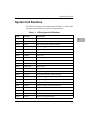
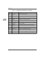


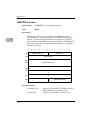

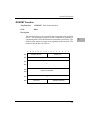
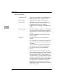

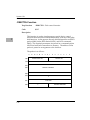
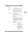
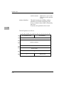


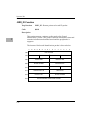


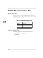


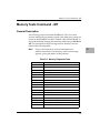


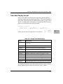


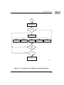


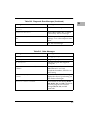


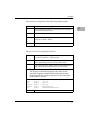

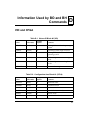
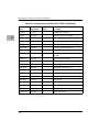

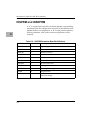
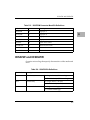

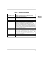

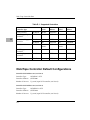


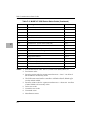
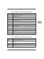

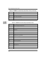


![[U2.01.02] Notice d`utilisation des conditions aux limites traitées par](http://vs1.manualzilla.com/store/data/006364897_1-a5498f87ef69237a965ecd943b6bd6dc-150x150.png)