1
AN333
CS470xx Firmware User’s Manual:
General Overview and Common Firmware Modules
Contents
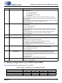
Overview
Document Strategy
This document provides a description of the operation of
firmware for the CS470xx family of DSPs and attempts to
explain frequently used terminology and, at the same time,
systematically explains the OS operation and
communication for the CS470xx.
Overview
Firmware Messaging
OS Firmware Module
This document is a general overview to the family of
CS470xx Firmware User’s Manuals designated by the
general name AN333[X][Y]; where [X] = MPM (matrix
processing module), VPM (virtual processing module),
PPM (post processing module), and [Y] = A,B,C. The
CS470xx family of DSPs does not contain a compressed
data decoder.
Audio Manager Firmware Module
PCM Firmware Module
Watchdog Timer
Document Revisions
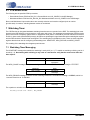
n
PCM inputs
Matrix Processor Module
Downsampler
Virtualizer Processor
Mid-Processor Overlay
Module
Crossbar
Dolby Headphone®
Virtualizer Processor Overlay
Matrix Processor Overlay
Audio Manager
Module
Tone
Control
Module
ID = 0xD4
Bass
Management
Module
Re-EQ™
Module
Parametric
EQ
Module
ID = 0xD5
Delay
Module
Includes:
Gain (master)
Mute (master)
Channel Trim
Channel Remap
ID = 0xD9
Up-sampler
PCM Outputs
ID = 0x83
Post-Processor Overlay (with APP loaded)
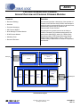
CS470xx Block Diagram
http://www.cirrus.com
Copyright Cirrus Logic, Inc. 2011
(All Rights Reserved)
AN333RC11
SEP '11
1 Document Strategy
1 Document Strategy
The CS470xx has been designed with inherently flexibility in terms of firmware usage. Each instance of operation of the
CS470xx can potentially use a different mix of DSP firmware, depending on the needs of the end user. The strategy
adopted to document the various DSP firmware is based on a single general overview firmware user’s manual coupled
with an individual application note for each DSP firmware module offered by Cirrus Logic.
The individual application notes each follow as an extension of AN333. These manuals have been named in such a way
so as to classify them into one of the following categories:
•
Operating system and general overview
•
Matrix processing module (MPM)
•
Virtual processing module (VPM)
•
Post-processing module (PPM)
Furthermore, since each classification such as post-processing module) may contain several associated DSP
firmware modules, an incremental letter assignment (such as A, B, C) was given to index each DSP firmware
document within a given category. As an example, the table below outlines the general naming conventions for
several firmware documents.
Table 1-1. Naming Conventions
DSP Firmware Module
General Overview, Operating System
and Common Firmware Modules
Delay Module
Crossbar Mixer Module
Dolby Headphone 2
Base Name
AN333
Overlay Type
(General)
Index
—
Document Reference Number
AN333
AN333
AN333
AN333
Post Processing Module (PPM)
Matrix Processing Module (MPM)
Virtual Processing Module (VPM)
a
c
a
AN333PPMA
AN333MPMC
AN333VPMA
For a further breakdown of the available CS470xx firmware modules and their respective application note
document numbers, see Section 2.3. Contact your local field applications engineer (FAE) for the latest code
updates and availability.
AN333RC11
2
2 Overview
2 Overview
The firmware that runs on this device expects a stereo or multichannel PCM input source. This section describes the
overlays.
The DSP program memory is divided into five functional segments called overlays that can be thought of as the locations
for the firmware modules that are accessed and implemented by the DSP. Firmware modules are downloaded into their
respective overlays either from internal ROM, or from the host.
•
OS Overlay
Manages the overall operation of the DSP. Also handles host communication, data inputs and outputs, and other
critical internal tasks.
•
Decoder Overlay
The decoder overlay on CS47xx only supports the Dolby Digital® decoder in certain memory maps.
•
Matrix Processing Overlay
Performs additional channel generation, upmixing, and downmixing. This overlay is where algorithms such as
Dolby® Pro Logic® IIx and Cirrus Original Multichannel Surround 2™ (COMS-2) reside.
•
Virtual Processing Overlay
Performs stereo virtualizing to simulate multichannel systems, such as Dolby® Audistry, Dolby Headphone®, and
Dolby Virtual Surround™.
•
Post-processing Overlay
This overlay specifically caters to firmware that performs post-processing tasks. It allows the system designer
flexibility in tweaking the system for optimal audio performance and effects. This is also the segment in which
firmware modules such as the Audio Manager, Bass Manager, Tone Control, Delay, and Parametric EQ Module
reside.
2.1 Code Image (.uld) Files
Each overlay is a separate code image file (.uld) that is loaded individually into the DSP. To change the functionality of the
application, only the overlay of interest needs to be loaded. For example the post-processing overlay can be exchanged
from SPP to APP by reloading only the post-processing overlay. This reduces the system response time to user changes,
as well as the code image storage requirements.
There are four different memory configurations of the program RAM size, denoted by p2, p4, p6, and p8 (p for program
memory; 2, 4, 6, and 8 are the number of kilowords; 1 word = 32 bits). Increasing P RAM decreases Y RAM, while X RAM
remains the same. Each overlay is denoted as p2, p4, p6, or p8 in the .uld file name to indicate which memory configuration
is used. For example, “ac3_p2_xxx.uld”.
Memory configuration must be consistent across all overlays (OS, decoder, MPM, VPM, and PPM).
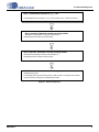
2.2 Download Sequence
A standard procedure to download firmware to the DSP follows this structure at system power-up:
3
AN333RC11
2.2 Download Sequence
Step 1: Download the firmware OS _p*_**.uld
Automatically fills the OS overlay. (*2, 4, 6, or 8 for memory map ; **device and version)
Step 2 (optional ): Download a matrix processing module
(Examples: Crossbar Mixer, Pro Logic IIx, DTS Neo:6®)
Automatically fills the matrix processing overlay.
Step 3 (optional): Download a virtual processing module
(Examples: Dolby Headphone, Dolby Virtual Speaker™)
Automatically fills the virtual processing overlay.
Step 4: Download a post -processor module group
(Examples: SPP, APP)
Automatically fills the post-processing overlay. If SPP or APP is not required, then the bare
requirement for this overlay is the Audio Manager module .
Figure 2-1. Download Sequence
AN333RC11
4
AN333RC11
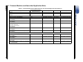
2.3 Firmware Modules and Associated Application Notes
Table 2-1. Firmware Module Read and Write Addresses with Associated Application Note Reference
DSP Firmware Module / (Application Note Name)
General
OS Manager
(AN333)
Matrix Processing Overlay
Dolby Pro Logic IIx (AN333MPMA)
DTS Neo:6
(AN333MPMB)
Crossbar
(AN333MPMC)
SRS® Circle Surround®
SRS Circle Surround II
SRS Circle Surround Auto
(AN333MPMG)
Signal Generator
(AN333MPMH)
Cirrus Original Multichannel Surround 2 (COMS-2)
(AN333MPMJ)
Virtual Processor Overlay
SRS TruSurround XT®
(AN333VPMH)
Dolby Headphone 2
(AN333VPMK)
Dolby Virtual Speaker 2
(AN333VPML)
SRS® TruSurround HD4™ Modules (with SRS WOW
HD®) (AN333VPMM)
Supported Memory Map(s)
(Firmware Version)
Write Request
Read Request
Read Response
01, 03, 05, 07, 09
0x8100HHHH 0xhhhhhhhh 0x81C0HHHH
0x01C0HHHH 0xhhhhhhhh
01, 07
01
0xBF00HHHH 0xhhhhhhhh 0xBFC0HHHH
0xB500HHHH 0xhhhhhhhh 0xB5C0HHHH
0x3FC0HHHH 0xhhhhhhhh
0x35C0HHHH 0xhhhhhhhh
01, 03, 05, 07, 09
0xDB00HHHH 0xhhhhhhhh 0xDBC0HHHH;
0x5BC0HHHH 0xhhhhhhhh
03, 05
0xB300HHHH 0xhhhhhhhh 0xB3C0HHHH
0x33C0HHHH 0xhhhhhhhh
01, 03
0x9A00HHHH 0xhhhhhhhh 0x9AC0HHHH
0x1AC0HHHH 0xhhhhhhhh
03
0xD300HHHH 0xhhhhhhhh 0xD3C0HHHH
0x53C0HHHH 0xhhhhhhhh
01
0xBA00HHHH 0xhhhhhhhh 0xBAC0HHHH
0x3AC0HHHH 0xhhhhhhhh
01
0xC000HHHH 0xhhhhhhhh 0xC0C0HHHH
0x40C0HHHH 0xhhhhhhhh
01
0xC100HHHH 0xhhhhhhhh 0xC1C0HHHH
0x41C0HHHH 0xhhhhhhhh
05
0xB300HHHH 0xhhhhhhhh 0xB3C0HHHH
0x33C0HHHH 0xhhhhhhhh
5
6
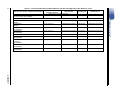
Table 2-1. Firmware Module Read and Write Addresses with Associated Application Note Reference (Cont.)
DSP Firmware Module / (Application Note Name)
Supported Memory Map(s)
(Firmware Version)
Write Request
Read Request
Read Response
Virtual Processor Overlay (continued)
Cirrus Virtualization Technology (CVT) - Virtualizer
Processor Module (AN333VPMN)
Post-processing Overlays
Audio Manager
(AN333)
PCM Manager
(AN333)
Delay
(AN333PPMA)
Bass Manager
(AN333PPMB)
Cirrus Band XpandeR (BXR) (AN333PPMC)
Cirrus Dynamic Volume Leveler (DVL)
(AN333PPMD)
EQ Module with PEQ and Direct Coefficient Mode
(11-bands)
(AN333PPME)
Tone Control
(AN333PPMF)
Cinema Re-EQ™
(AN333PPMK)
09
0xC100HHHH 0xhhhhhhhh 0xC1C0HHHH
0x41C0HHHH 0xhhhhhhhh
01, 03, 05, 07, 09
0x8300HHHH 0xhhhhhhhh
0x03c0HHHH 0xhhhhhhhh
01, 03, 05, 07, 09
0x9B00HHHH 0xhhhhhhhh 0x9BC0HHHH
0x1BC0HHHH 0xhhhhhhhh
01, 03, 05, 07, 09
0xD900HHHH 0xhhhhhhhh 0xD9C0HHHH
0x59C0HHHH 0xhhhhhhhh
01, 03, 05, 07, 09
0xD700HHHH 0xhhhhhhhh 0xD7C0HHHH
0x57C0HHHH 0xhhhhhhhh
01
01
0xE700HHHH 0xhhhhhhhh 0xE7C0HHHH
0xE600HHHH 0xhhhhhhhh 0xE6C0HHHH
0x67C0HHHH 0xhhhhhhhh
0x67C0HHHH 0xhhhhhhhh
01, 03, 05, 07, 09
0xD500HHHH 0xhhhhhhhh 0xD5C0HHHH
0x55C0HHHH 0xhhhhhhhh
01, 03, 05, 07, 09
0xD400HHHH 0xhhhhhhhh 0xD4C0HHHH
0x54C0HHHH 0xhhhhhhhh
01, 03
0xDC00HHHH 0xhhhhhhhh 0xDCC0HHHH
0x5CC0HHHH 0xhhhhhhhh
0x83c0HHHH
AN333RC11
7
Table 2-1. Firmware Module Read and Write Addresses with Associated Application Note Reference (Cont.)
DSP Firmware Module / (Application Note Name)
Supported Memory Map(s)
(Firmware Version)
Write Request
Read Request
Read Response
Post-processing Overlays (continued)
SPP (Standard Post Processing) in DSP Composer
Module Processing Order:
1. Tone Control
2. BM
3. Delay
4. AM
See individual module application notes.
APP (Advanced Post Processing) in DSP Composer
Module Processing Order:
1. Tone Control
2. ReEQ
3. BM
4. EQ
5. Delay
6. AM
See individual module application notes.
01, 03, 05, 07, 09
—
—
—
01, 03
—
—
—
AN333RC11
3 Firmware Messaging
3 Firmware Messaging
While using the CS470xx it is necessary to communicate with the DSP in order to control or monitor the various
downloaded firmware modules. We refer to this process of communication as firmware messaging. The purpose of this
section is to describe the types and formats of these firmware messages. In general, the user can control the firmware
module running on the DSP with firmware messaging, and subsequently perform various tasks including the following:
•
Configure the module after firmware download (such as kick-starting the DSP)
•
Change run-time parameters (such as adjusting the volume or switching Pro Logic II modes)
•
Obtain information from the DSP (such as the current state of the firmware registers or data stream information)
3.1 Communication Overview
From a microprogramming point of view, the CS470xx firmware modules can be thought of as blocks of several 32-bit
registers (variables) that either control the behavior of the firmware or store information about the state of the firmware at
the time of operation. Each register has a unique index. Access to the register involves a combination of a specified opcode
for that firmware module together with the register index. For each firmware module, the following opcodes are available:
•
Write Opcode—Issues a command to write to a specific module.
•
Read Opcode—Issues a command to read from a specific module.
•
Read-response Opcode—Indicates the module and index that have been read.
These available opcodes permit the following types of communication with the CS470xx DSP:
•
Writing to the DSP
•
Solicited read from the DSP
•
Unsolicited read from the DSP
3.1.1
Writing to the DSP
A write session with the CS470xx consists of one 8-byte message from the host to the CS470xx. The write
message consists of a 32-bit command word followed by a 32-bit data word (that is, data to be written to the
register). The command word is formed by combining the write opcode for that module with the index of the
register that needs to be written. The 32-bit data word is the value of the data intended to fill that register.
Fig. 3-1 shows the format of a write message:
Write Command Word:
31 30 29 28 27 26 25 24 23 22 21 20 19 18 17 16 15 14 13 12 11 10 9
OPCODE[31:16]
8
7
6
5
4
3
2
1
0
5
4
3
2
1
0
INDEX[15:0]
Write Data Word:
31 30 29 28 27 26 25 24 23 22 21 20 19 18 17 16 15 14 13 12 11 10 9
8
7
6
DATA WORD[31:0]
Figure 3-1. Write Command and Write Data Words
3.1.2
Solicited Read
A solicited read can be thought of as a request to read the contents of a specific register. A solicited read is composed of
a 32-bit solicited read-command word, which is a request to read a specific index (register) in a given module or read up
to sixteen consecutive indices. The DSP, upon receiving this message, responds by sending back a 32-bit read-response
opcode and the requested 32-bit data word(s) contained in each of the indices read.
AN333RC11
8
4 Operating System (OS) Firmware Module
Fig. 3-2 provides the format of a solicited read message:
Read Command Word:
31 30 29 28 27 26 25 24 23 22 21 20 19 18 17 16 15 14 13 12 11 10 9
OPCODE[31:16] (Bits 31:24 = Module ID+0x80, bits 23:20 =
0xc, bits 19:16 = <num of indices – 1>)
8
7
6
5
4
3
2
1
0
2
1
0
2
1
0
INDEX[15:0] (First index to be read)
Figure 3-2. Read Command Data Word
Fig. 3-3 provides the format of a solicited read message:
Read-Response Command Word:
31 30 29 28 27 26 25 24 23 22 21 20 19 18 17 16 15 14 13 12 11 10 9
OPCODE[31:16] (Bits 31:24= Module ID, Bits 23:20 =0xc,
Bits 19:16= <num of indices – 1>)
8
7
6
5
4
3
INDEX[15:0] (First index to be read)
Read-Response Data Word(s):
31 30 29 28 27 26 25 24 23 22 21 20 19 18 17 16 15 14 13 12 11 10 9
8
7
6
5
4
3
DATA WORD[31:0]
Figure 3-3. Read-Response Command and Read-response Data Words
3.1.3
Unsolicited Message
The DSP needs to inform the host when the PLL is out of lock or there is a run-time memory allocation error (malloc failure).
This type of message is considered an unsolicited message because it was initiated by the CS470xx rather than the host.
This message comes from the CS470xx to indicate a change in the system that must be addressed. The 8-byte unsolicited
read messages from the CS470xx consists of a 4-byte read command word, which defines the type of unsolicited
message, and an associated 4-byte data word that contains more information describing a system condition. When the
IRQ pin for the port being used goes low (SCP1_IRQ or PCP_IRQ), the host senses that an unsolicited message is ready
to be read. Every time a message is detected, the host reads out the 8-byte unsolicited read message.
4 Operating System (OS) Firmware Module
Unsolicited Read Command Word:
31 30 29 28 27 26 25 24 23 22 21 20 19 18 17 16 15 14 13 12 11 10 9
OPCODE[31:16]
8
7
6
5
4
3
2
1
0
5
4
3
2
1
0
INDEX[15:0]
Unsolicited Read Data Word:
31 30 29 28 27 26 25 24 23 22 21 20 19 18 17 16 15 14 13 12 11 10 9
8
7
6
DATA WORD[31:0]
Figure 4-1. Unsolicited Read Command and Data Words
Table 4-1 describes the API used to control the OS firmware module. Indices of the Firmware Module can differ in
properties that are important to the system firmware programmer.
Variables marked by a ‘†’ can be modified after kick-starting the application. However, variables NOT marked by a ‘†’ must
be configured by the system host controller before the kick-start message is sent to begin decoding. For these indices,
changes after kick-starting the application do not have the desired effect and can potentially cause the application to
become unstable.
All indices are re-initialized to the default values after downloading the overlay and soft-resetting the overlay.
Index = 0xHHHH, data value = 0xhhhhhhhh
Write = 0x8100HHHH 0xhhhhhhhh
9
AN333RC11
4 Operating System (OS) Firmware Module
Read Request = 0x81C0HHHH
Read Response = 0x01C0HHHH 0xhhhhhhhh
Table 4-1. OS Firmware Manager
Index
0x0000
Variable
KICKSTART
0x0001
0x0002
IO_CONFIG
OUTPUT_MODE_CONTROL†
AN333RC11
Description
Bit 16: 0/1 Disable/enable malloc failure reporting.
Bit 13: 0/1 Disable/enable continual GPIO updating.
Only applicable if Bit 12 is set. If Bit 12 is disabled, audio pins are be available.
Bit 12: 0/1 Disable/enable GPIO updates.
Bit 9: 0/1 Disable/enable hardware watchdog timer reload.
Bit 8: 0/1 Disable/enable hardware watchdog timer.
When Bit 8 is set, the hardware watchdog timer is enabled. When the watchdog timer is
enabled, the timer with the initial set value starts decrementing, and when it reaches zero, it
stops decrementing and resets the hardware. Every 16 audio samples, there is an option to
reload the watchdog timer, controlled by bit 9. If bit 9 is set, a watchdog timer reload does
not take place. Otherwise, the counter is reloaded with the set value every 16 audio samples.
Bit 0: Kick-start: Set to 1 to trigger kick-start
Default = 0x00000000
See Section 4.2 for the details of this index.
Bits 7:4 Dual Mono Mode (valid only if input mode is 0x0000)
0x0 = Stereo Mode => Center_out = None
Left_out = Left_in
Right_out = Right_in
0x1 = Left Mono => Center_out = Left_in
Left_out = None
Right_out = None
0x2 = Right Mono => Center_out = Right_in
Left_out = None
Right_out = None
0x3 = Mixed Mono => Center_out = (Lin+Rin)/2
Left_out = None
Right_out = None
For non-zero values (1,2 or 3) in bits 7:4 of the OUTPUT_MODE_CONTROL variable,
values in bits 3:0 are ignored.
Dual mono mode selection is available only if input mode is 0, that is for dual mono streams.
Bits 3:0 Output Mode (number of speakers present in the system)
0x0 = 2/0 Lt, Rt Dolby Surround compatible
0x1 = 1/0 C
0x2 = 2/0 L/R
If the output mode is set to 0x02 and Dolby decoding is also set, then the output is Lt/Rt or
Lo/Ro depending on the setting of the AC3 Manager STEREO_MODE_CONTROL. See
AN333DA for more information.
0x3 = 3/0 L/C/R
0x4 = 2/1 L/R/S
0x5 = 3/1 L/C/R/S
0x6 = 2/2 L/R/Ls/Rs
0x7 = 3/2 L/C/R/Ls/Rs
0x8 = 3/3 L/C/R/Ls/Rs/Cs
0x9 = 3/4 L/C/R/Ls/Rs/Sbl/Sbr
0xA = 2/3 L/R/Ls/Rs/Cs
0xB = 2/4 L/R/Ls/Rs/Sbl/Sbr
Default = 0x00000007
10
4 Operating System (OS) Firmware Module
Table 4-1. OS Firmware Manager (Cont.)
Index
0x0003
Variable
SAMPLE_RATE†
0x0004
–
0x0008
0x0009
Reserved
SOFTBOOT†
0x000A
–
0x003A
0x003B
Reserved
0x003C
GPIO_OE
0x003D
GPIO_MUX
0x003E
–
0x0043
Reserved
11
GPIO_D
Description
The host must set the sample rate variable to inform firmware modules of the sample rate.
Some firmware modules use this information to calculate correct coefficients or use the
correct table data. The actual sample rate is determined by the DAO_LRCLK, which can be
configured to be master or slave. If the DAO_LRCLK is master, the sample_rate can be set
using the DAO clock dividers. See the CS470xx Hardware User’s Manual for more
information.
Bits 3:0 Sample Rate
0x0 = 48 kHz
0x1 = 44.1 kHz
0x2 = 32 kHz
0x3 = Reserved
0x4 = 96 kHz
0x5 = 88.2 kHz
0x6 = 64 kHz
0x7 = Reserved
0x8 = 24 kHz
0x9 = 22.05 kHz
0xA = 16 kHz
0xB = Reserved
0xC = 192 kHz
0xD = 176.4 kHz
0xE = 128 kHz
0xF = Reserved
Default = 0x00000000 (48 kHz)
Reserved
Bit 4: 1 = Engage low-power mode.
Bit 0: 0/1 disable/initiate soft boot sequence.
After a soft boot is initiated, the OS sends a 0x00000005 (SOFT_BOOT_ACK) to the host.
The host can then use the standard boot protocol to download one or more overlays. After a
soft boot is initiated, the OS will respond to boot protocol messages only.
The bit is reset to 0 after the soft boot is complete.
Default = 0x00000000
Reserved
GPIO data register.
Bits 31:0
Bit[i] corresponds to pin GPIO[i] (i=0,...,31).
Both the GPIO_OE and GPIO_MUX must be set to 1 for a particular bit before that bit can
be written. Bit 13 and 12 of KICKSTART variable must be set to 1(enabled).
GPIO data direction register.
Bits 31:0
When Bit[i] is 1, pin GPIO[i] is configured as an output. When Bit[i] is 0, pin GPIO[i] is
configured as an input. (i=0,...,31).
GPIO MUX Selector register.
Bits 31:0
When Bit[i] is 1, pin GPIO[i] is a GPIO function. When Bit[i] is 0, pin GPIO[i] is overwritten by
the other function on that pin. Also, when Bit[i] is 0, Bit[i] of the GPIO_D register is not
writable
Reserved
AN333RC11
4 Operating System (OS) Firmware Module
Table 4-1. OS Firmware Manager (Cont.)
Index
0x0044
Variable
PLL_STANDARD_CONFIG
0x0045
PLL_CUSTOM_CONFIG0
0x0046
PLL_CUSTOM_CONFIG1
0x0047
–
0x004E
0x004F
Reserved
0x0050
–
0x0054
0x0055
0x0056
–
0x0058
AN333RC11
SW_NUM_CHANS
Reserved
MALLOC_SUCCESS_AND_
ATTEMPT_COUNTS
Reserved
Description
Bits 11:4 Reference Clock Frequency is the frequency of clock attached to XTI pin, must be
set:
0x00 = 12.288 MHz
0x01 = 24.576 MHz
0x02–0x0F = Reserved
0x10 = 18.432 MHz
0x11 = 27 MHz
0x12–0xFF = Reserved
Bits 3:0 DSP core speed:
0x0 = Custom speed.
0x1 = 101 MHz (Max Ambient Temperature = 105 C)
0x3 = Reserved
0x5 = 152 MHz (Max Ambient Temperature = 85C)
0x2, 0x4, 0x6–0xF = Reserved
Default = 0x00000011
Bits 31:0 PLL Custom Configuration 0:
0x00002402 - 11.2896 MHz - 101 Core Speed
0x00002B02 - 11.2896 MHz - 122 Core Speed
0x00002302 - 11.2896 MHz - 130 Core Speed
0x00002802 - 11.2896 MHz - 152 Core Speed
0x00002002 - 12.288 MHz - 130 Core Speed
0x00001502 - 18.432 MHz - 130 Core Speed
0x80000000 - 24.576 MHz - 130 Core Speed
0x74000000 - 27.000 MHz - 130 Core Speed
PLL1_CUSTOM_CONFIG0: Setting of fract_in in register CLKREG9 of PLL1 (fract_in is in
1.31 unsigned fractional format, range: 1.000 to 1.9999….) VCO1_CLK = fract_in * 32 *
REF_CLK
Bits 31:0 PLL Custom Configuration 1:
0x00000333 - 101 or 122 Core Speed
0x00000233 - 130 Core Speed
PLL1_CUSTOM_CONFIG1
Setting of CLKREG17 register of PLL1
Setting of OVFS_MUX, HCLK_MUX, OVFS_DIV1, OVFS_DIV2, HCLK_DIV for the DSP
Clock and I2S_OVFS Clock.
OVFS_MUX selects divided VCO_CLK for I2S_OVFS_CLK, else it is REF_CLK.
HCLK_MUX selects divided VCO_CLK for DSP_HCLK, else it is REF_CLK.
I2S_OVFS_CLK = VCO_CLK / (2 * (OVFS_DIV1+1) * (OVFS_DIV2 + 1))
DSP_CLK = VC0_CLK / (2 * (HCLK_DIV+1)
Reserved
Number of software audio channels to be supported in OS I/O buffers.
Bits 5:0 Number of channels. Maximum supported is 16.
Default: 0x00000008
Reserved
Bits 31:16 Number of successful memory allocations.
Bits 15:0 Number of memory allocation attempts.
Reserved
12
4 Operating System (OS) Firmware Module
Table 4-1. OS Firmware Manager (Cont.)
Index
0x0059
Variable
SCP_CONTROL
0x005D
PLL1_CUSTOM_CONFIG2
0x005E
PLL2_CUSTOM_CONFIG0
0x005F
PLL2_CUSTOM_CONFIG1
0x0060
PLL2_CUSTOM_CONFIG2
0x006D
ADC_USER_MODES
0x006E
DAC_USER_MODES
0x006F
Reserved
13
Description
Post pre-kick-start mode of SCP communication
Bits 2 1 0
0 0 0 => I2C Master (Supported for firmware versions V01, V03 only)
0 0 1 => SPI Master (Supported for firmware versions V01, V03 only)
1 0 0 => I2C Slave
1 0 1 => SPI Slave
Default: 0x00000000
Setting of CLKREG19 register of PLL1
Setting of PLL_DIV_FF for ADC_DAC CLK
ADC_DAC_CLK = VC01_CLK / PLL1_DIV_FF
Setting of fract_in in register CLK2REG9 of PLL2
(fract_in is in 1.31 unsigned fractional format Range: 1.000 to 1.9999….)
VCO2_CLK = fract_in * 32 * REF_CLK
Setting of CLK2REG17 register of PLL2
Setting OVFS_MUX, OVFS_DIV1, OVFS_DIV2, for SPDIFRX_OVFS Clock.
OVFS_MUX selects divided VCO_CLK for SPDIFRX_OVFS_CLK, else it is REF_CLK.
SPDIFRX_OVFS_CLK = VCO_CLK / (2 * (OVFS_DIV1+1) * (OVFS_DIV2 + 1))
DSP_CLK = VC0_CLK / (2 * (HCLK_DIV+1))
Setting of CLK2REG18 of PLL2
Selects VCO1 or VCO2 source for HCLK, I2S_OVFS_CLK, and SPDIF_RX_OVFS_CLK.
Also sets divider value for SRC_CLK
SRC_CLK = SPDIF_RX_OVFS_CLK / (SRC_CLK_DIV + 1)
Setting of ADC_USER_MODE. Bits [18:9] can be changed during runtime.
Bits 0:3 ADC_ENABLE for ADCs
1 Enable
0 Disable
Bit 4
1 Enables single-ended operation for all ADCs
0 Differential operation for all ADCs
Bit 5:8 Reserved
Bits 9:13 MUX_SELECT_CH2–ADC
0x01 AIN2A
0x02 AIN3A
0x04 AIN4A
0x08 AIN5A
0x10 AIN6A
Bits 14:18 MUX_SELECT_CH3–ADC
0x01- AIN2B
0x02- AIN3B
0x04- AIN4B
0x08- AIN5B
0x10- AIN6B
Bit 19:31 Reserved
Default: 0x0000 423F
Bits 3:0 are the DAC_ENABLES (1 = enabled)
Bit 0 = DAC outputs AOUT_1 and AOUT_2
Bit 1 = DAC outputs AOUT_3 and AOUT_4
Bit 2 = DAC outputs AOUT_5 and AOUT_6
Bit 3 = DAC outputs AOUT_7 and AOUT_8
Other bits are reserved and set to 0, except bits 23 and 24 are reserved and set to 1.
Reserved
AN333RC11
4.1 Memory Configurations for IO_CONFIG (Index 0x0001)
Table 4-1. OS Firmware Manager (Cont.)
Index
0x0070
0x0071
0x0074
0x0075
0x0076
0x0077
0x0078
Variable
DACSRC_FSI_SEL
Description
Bits 31:2 Reserved
Bits 1:0 FSI Select:
0x0 - FSI = SPDIFRX_LRCLK
0x1 - FSI = DAI1_LRCLK
0x2 - FSI = DAO1_LRCLK (default)
0x3 - Reserved
When output APBSRC is enabled, it must be ensured that DACSRC_FSI_SEL and
OUTPUT_APBSRC_FSI_SEL is the same which could come from either DAI_LRCLK or
SPDIFRX_LRCLK.
When output APBSRC is not enabled, variable OUTPUT_APBSRC_FSI_SEL is irrelevant,
however DACSRC_FSI_SEL must be set to 2 (DAO1_LRCLK).
Default = 0x0000 0002
OUTPUT_APBSRC_FSI_SEL
Bits 31:1 Reserved
Bit 0 FSI Select:
0x0 - FSI = SPDIFRX_LRCLK
0x1 - FSI = DAI1_LRCLK
1. When output APBSRC is enabled, it must be ensured that DACSRC_FSI_SEL and
OUTPUT_APBSRC_FSI_SEL is the same which could come from either DAI_LRCLK or
SPDIFRX_LRCLK.
2. When output APBSRC is not enabled, variable OUTPUT_APBSRC_FSI_SEL is
irrelevant, however DACSRC_FSI_SEL must be set to 2 (DAO1_LRCLK).
Default = 0x0000 0000
PCM_MANUAL_CONFIG
0/1: Manually Disable/Enable PCM. Autodetect will not have any effect if this is enabled
Default: 0x00000000
PCM_AUTOSWITCH_CONFIG Bit 0 0/1 Disable/Enable automatic switching to/from PCM Decoder.
Notes:
1) Autodetect must be enabled to use this feature.
2) Valid for Stereo I²S or SPDIF compressed IO_CONFIG values ONLY.”
3) PCM Manager must be enabled to use this feature.
4) If IO_CONFIG is PCM in through SPDIF-RX, Output APBSRC must be enabled.
Default: 0x00000001
AUTODETECT_CONFIG
Bit 2 0/1 Disable/Enable Audio Configuration Change Notification (ACCN).
Bit 1 0/1 Disable/Enable bypassing of autodetection at application restart.
Bit 0 0/1 Disable/Enable autodetection
Default = 0x00000001
PCM_AUTODETECT_SILENCE_ Bits 31:0 Number of samples (Left+Right) of silence upon which the DSP will declare
THRESHOLD
Silence while having detected and currently playing PCM (Autodetect is enabled).
Valid for all decoders when configured for PCM pass-through and auto switch. It is
recommended that system designers set this value large enough to avoid inter-track silence
from PCM compact discs.
Default = 0x00017700
(The default allows for 1 sec of inter-track silence at 48 Khz).
SPDIF_RX_STATUS
S/PDIF Rx Lock: 0x00000040
S/PDIF Rx Unlock: 0x00000041
4.1 Memory Configurations for IO_CONFIG (Index 0x0001)
Table 4-2 shows the memory configurations for IO_CONFIG.
Table 4-2. Memory Configurations for IO_CONFIG (Index 0x0001)
Firmware Version
V01
V03
V05
V07
AN333RC11
P8
P8
—
P8
Memory Configurations
P10
P12
P10
P12
—
—
—
—
P14
P14
P14
—
14
4.2 Details of Index 0x0001
Table 4-2. Memory Configurations for IO_CONFIG (Index 0x0001)
Firmware Version
V09
V11
V13
Memory Configurations
—
P12
P10
—
—
P12
—
—
—
—
—
—
4.2 Details of Index 0x0001
Table 4-3. IO_CONFIG Bits 15:0 (Index 0x0001)
Input Configuration (IO_CONFIG Bits 15:0)
0001 8-ch I²S PCM
0002 2-ch I²S PCM
Firmware Version
V01
V03
V05
V07
V09
V11
V13
V01
V03
V05
V07
V09
V11
V13
SRC1
V01
V03
V05
V07
V09
V11
V13
0008 2-ch I²S PCM with SRC1
V01
V03
V05
V07
V09
V11
V13
0004 8-ch I²S PCM with
0010 ADC + 2-ch I²S PCM with
SRC1
V01
V03
—
—
—
—
—
0020 Reserved
—
—
—
—
—
—
—
0040 Reserved
—
—
—
—
—
—
—
0080 Reserved
—
—
—
—
—
—
—
0100 I²S Compressed
—
—
V05
V07
V09
V11
V13
0200 S/PDIF Compressed
—
—
V05
V07
V09
V11
V13
0400 2-ch ADC + 10-ch I²S PCM
V01
V03
—
—
—
—
—
0800 ADC + 8-ch I²S PCM
V01
V03
—
—
—
—
—
1000 ADC
V01
V03
V05
V07
V09
V11
V13
2000 S/PDIF PCM
V01
V03
V05
V07
V09
V11
V13
4000 ADC + S/PDIF PCM
V01
V03
—
—
—
—
—
8000 ADC + 8-ch I²S + S/PDIF- PCM
V01
V03
—
—
—
—
—
1. With these configurations, you cannot select DAO with Output SRC.
Table 4-4. IO_CONFIG Bits 31:16 (Index 0x0001)
Output Configuration (IO_CONFIG Bits 31:16)
Firmware Version
0001 DAC Output
V01
V03
V05
V07
V09
V11
V13
0010 8-ch I²S PCM
V01
V03
V05
V07
V09
V11
V13
0100 DAO2 S/PDIF PCM Only
V01
V03
—
—
—
—
—
1000 8-ch I²S with SRC
V01
V03
—
—
—
—
—
—
—
—
V07
—
V11
V13
2000 Auxiliary ADC Input1
1. Supported only for stereo PCM/compressed configurations. For LO I/O configurations 0002, 0200, 0100, and
2000.
Table 4-5. Input Configurations versus Slot index for Setting Up Input Channel Remap
Configurable Input Channel Map
Bits 31:16 I/O Configuration
20xx: Additional ADC Input
15
PCM
Manager
Index
Input Port
IO_BUFFER_SOURCE
9
ADC-0
8
10
ADC-1
9
11
ADC-2
10
12
ADC-3
11
AN333RC11
4.2 Details of Index 0x0001
Table 4-5. Input Configurations versus Slot index for Setting Up Input Channel Remap (Cont.)
Configurable Input Channel Map
Bits 15:0 I/O Configuration
0001: 8-ch DAI/I2S PCM
0004: 8-channel DAI/I2S PCM with SRC
PCM
Manager
Index
Input Port
IO_BUFFER_SOURCE
1
DAI0 left subframe word
0
2
DAI0 right subframe word
1
3
DAI1 left subframe word
2
4
DAI1 right subframe word
3
5
DAI2 left subframe word
4
6
DAI2 right subframe word
5
7
DAI3 left subframe word
6
8
DAI3 right subframe word
7
Bits 15:0 I/O Configuration
0002: 2-channel DAI/I2S PCM
0100: 2-channel DAI/I2S PCM
0008: 2-channel DAI/I2S PCM with SRC
1
DAI4 left subframe word
0
2
DAI4 right subframe word
1
Bits 15:0 I/O Configuration
0010: 4-channel channel ADC Input + 2-CH I²S with
SRC
1
ADC1 left channel
0
2
ADC1 right channel
1
3
ADC2 left channel
2
4
ADC2 right channel
3
5
DAI0 left subframe word
4
6
DAI0 right subframe word
5
1
ADC1 left channel
0
2
ADC1 right channel
1
3
ADC2 left channel
2
4
ADC2 right channel
3
1
DAI0 left subframe word
(S/PDIF Rx recovered
through DAI0)
0
2
DAI0 right subframe word
(S/PDIF Rx recovered
through DAI0)
1
1
ADC1 left channel
0
2
ADC1 right channel
1
3
ADC2 left channel
2
4
ADC2 right channel
3
5
DAI0 left subframe word
(S/PDIF Rx recovered
through DAI0)
4
6
DAI0 right subframe word
(S/PDIF Rx recovered
through DAI0)
5
Bits 15:0 I/O Configuration
1000: 4-channel channel ADC Input
Bits 15:0 I/O Configuration
2000: 2-channel S/PDIF Rx Input
0200: 2-channel S/PDIF Rx Input
Bits 15:0 I/O Configuration
4000: 4-channel ADC + 2-channel S/PDIF Rx Input
AN333RC11
16
4.2 Details of Index 0x0001
Table 4-5. Input Configurations versus Slot index for Setting Up Input Channel Remap (Cont.)
Configurable Input Channel Map
Bits 15:0 I/O Configuration
8000: 4-channel ADC + 8-channel DAI /I²S Input +
2-channel S/PDIF Rx Input
Bits 15:0 I/O Configuration
0800: 4-channel ADC + 8-channel DAI /I²S Input
17
PCM
Manager
Index
Input Port
IO_BUFFER_SOURCE
1
ADC1 left channel
0
2
ADC1 right channel
1
3
ADC2 left channel
2
4
ADC2 right channel
3
5
DAI1 left subframe word
4
6
DAI1 right subframe word
5
7
DAI2 left subframe word
6
8
DAI2 right subframe word
7
9
DAI3 left subframe word
8
10
DAI3 right subframe word
9
11
DAI4 left subframe word
10
12
DAI4 right subframe word
11
13
DAI0 left subframe word
(S/PDIF Rx recovered
through DAI0)
12
14
DAI0 right subframe word
(S/PDIF Rx recovered
through DAI0)
13
1
ADC1 left channel
0
2
ADC1 right channel
1
3
ADC2 left channel
2
4
ADC2 right channel
3
5
DAI0 left subframe word
4
6
DAI0 right subframe word
5
7
DAI1 left subframe word
6
8
DAI1 right subframe word
7
9
DAI2 left subframe word
8
10
DAI2 right subframe word
9
11
DAI3 left subframe word
10
12
DAI3 right subframe word
11
AN333RC11
4.3 OS Manager in DSP Composer
Table 4-5. Input Configurations versus Slot index for Setting Up Input Channel Remap (Cont.)
Configurable Input Channel Map
PCM
Manager
Index
Bits 15:0 I/O Configuration
0400: 2-channel ADC + 10-channel DAI /I²S Input
Input Port
IO_BUFFER_SOURCE
1
ADC2 left channel
0
2
ADC2 right channel
1
3
DAI0 left subframe word
2
4
DAI0 right subframe word
3
5
DAI1 left subframe word
4
6
DAI1 right subframe word
5
7
DAI2 left subframe word
6
8
DAI2 right subframe word
7
9
DAI3 left subframe word
8
10
DAI3 right subframe word
9
11
DAI4 left subframe word
10
12
DAI4 right subframe word
11
4.3 OS Manager in DSP Composer
Most configuration information described in Section 4 can be controlled in DSP Composer. The OS Manager
indices are available in the Audio In, Audio Out, and System blocks. To insert these, simply drag the Audio In,
Audio Out, and System blocks to the workspace. When the Audio In, Audio Out, and System blocks are on the
workspace, the pre-kick and run-time controls are accessible by double-clicking in the corresponding blocks.
The controls are adjustable during run-time to interact with the DSP in a similar way as would a host
microcontroller in an actual system. Fig. 5-2 shows that when you initially drag the Audio In block onto the
workspace, the Audio In Device Properties automatically pops up, prompting to the user to select the input
source and data format. This is also accessible by right-clicking the Audio In block.
4.4 Unsolicited Messages
Index = 0xHHHH, data value = 0xhhhhhhhh
No Write Message. No Read Request.
Unsolicited Read Response = 0x8100HHHH 0xhhhhhhhh
AN333RC11
18
4.4 Unsolicited Messages
Table 4-6. Unsolicited Messages
Index
0x0000
Message
MALLOC_FAILURE
0x0002
PLL_OUT_OF_LOCK
4.4.1
Description
Bits 19:16
1 = MALLOC_ERROR_REQ_LIST_OVERFLOW—too many requests.
2 = MALLOC_ERROR_NO_FREE_BLOCK—no non-modulo free block was available
to service next request)
3 = MALLOC_ERROR_NO_MOD_FREE_BLOCK—no modulo free block was
available to service next request)
Message= SPDIF_LOCK_UNLOCK
Bits 6:0
SPDIF LOCKED/SPDIF UNLOCKED unsolicited messages are applicable only if IO_
CONFIG bits 15:0 are set to 0x2000 or 0x02000.
0x40 SPDIF LOCKED
0x41 SPDIF UNLOCKED
Bit 23 1
Bits 22:0 Reserved.
Autodetection
Index = 0xHHHH, data value = 0xhhhhhhhh
No Write Command.
No Read Request Command.
Unsolicited Read Response = 0x8100HHHH 0xhhhhhhhh
Table 4-7. Autodetect Messages
Index
0x0000
19
Variable
AUTODETECT_RESPONSE
Description
Bit 31 = Decodable_Stream_Flag= 0/1 = This stream is not/is decodable by the
application (no need for new download if 1).
Bit 5 Non_IEC61937_Stream_Flag= 1/0 = This stream is not/is IEC61937
compressed data.
If Non_IEC61937_Stream_Flag=1
Bits [4:0] = Non_IEC61937 Stream Descriptor.
0x00 = Silent Input Data (Out of Application Sync).
0x01 = DTS Format-16 elementary stream.
0x02 = DTS Format-14 elementary stream.
0x03 = Linear PCM stream.
0x04 = HDCD PCM Sync Detect (only available in HDCD application).
0x05 = HDCD PCM Sync Lost (only available in HDCD application).
If Non_IEC61937_Stream_Flag=0
Bits [4:0] = IEC61937 Stream Descriptor = Identical to bits [4:0] of the Pc burst
data-type descriptor in IEC61937 specification. Description of the data-type field
of Pc reproduced below from IEC61937 Specification (current as of 11/97):
0x00 = Never Reported.
0x01 = AC-3 data.
0x03 = Never Reported.
0x04 = MPEG-1 Layer 1 data.
0x05 = MPEG-1 Layer 2 or 3 data or MPEG-2 without extension.
0x06 = MPEG-2 data with extension.
0x07 = MPEG-2 AAC ADTS data.
0x08 = MPEG-2 Layer 1 Low sampling frequency.
0x09 = MPEG-2 Layer 2 or 3 Low sampling frequency.
0x0B = DTS-1 data (512-sample bursts).
0x0C = DTS-2 data (1024-sample bursts).
0x0D = DTS-3 data (2048-sample bursts).
0x0E - 0x1B = Reserved.
0x1C = MPEG-2 AAC ADTS data.
AN333RC11
5 Audio Manager Firmware Module
5 Audio Manager Firmware Module
The Audio Manager Firmware module provides the ability for the microcontroller to easily manage general audio controls
such as gain, mute, trim and channel remap.
Index = 0xHHHH, data value = 0xhhhhhhhh
Write = 0x8300HHHH 0xhhhhhhhh
Read Request = 0x83c0HHHH;
Read Response = 0x03c0HHHH 0xhhhhhhhh
Table 5-1. Audio Manager
Index
0x0000
Variable
GAIN†
0x0001
MUTE†
0x0002
CHAN_0_TRIM†
0x0003
CHAN_1_TRIM†
0x0004
CHAN_2_TRIM†
0x0005
CHAN_3_TRIM†
0x0006
CHAN_4_TRIM†
0x0007
CHAN_5_TRIM†
0x0008
CHAN_6_TRIM†
0x0009
CHAN_7_TRIM†
0x000A
CHAN_8_TRIM†
0x000B
CHAN_9_TRIM†
0x000C
CHAN_10_TRIM†
0x000D
CHAN_11_TRIM†
0x000E
CHAN_12_TRIM†
AN333RC11
Description
0x00000000-0x7FFFFFFF (-inf. to +24 dB). Overall System Gain. Signed value with
decimal point to the right of bit 27. Range is zero to (16-2-27). Negative values can be
used to invert the phase of all the outputs.
Default = 0x08000000 (+0 dB)
0/1 = Unmute/Mute Audio
Default = 0x00000000 (unmuted)
0x00000000 – 0x80000000 (0.0 to 1.0)
Volume trim for channel 0 (Left Channel)
Default = 0x80000000
0x00000000 – 0x80000000 (0.0 to 1.0)
Volume trim for channel 1 (Center Channel)
Default = 0x80000000
0x00000000 – 0x80000000 (0.0 to 1.0)
Volume trim for channel 2 (Right Channel)
Default = 0x80000000
0x00000000 – 0x80000000 (0.0 to 1.0)
Volume trim for channel 3 (Left Surround Channel)
Default = 0x80000000
0x00000000 – 0x80000000 (0.0 to 1.0)
Volume trim for channel 4 (Right Surround Channel)
Default = 0x80000000
0x00000000 – 0x80000000 (0.0 to 1.0)
Volume trim for channel 5 (Left Surround Back Channel)
Default = 0x80000000
0x00000000 – 0x80000000 (0.0 to 1.0)
Volume trim for channel 6 (Right Surround Back Channel)
Default = 0x80000000
0x00000000 – 0x80000000 (0.0 to 1.0)
Volume trim for channel 7 (LFE0 Channel)
Default = 0x80000000
0x00000000 – 0x80000000 (0.0 to 1.0)
Volume trim for channel 8 (Left DualZone Channel)
Default = 0x80000000
0x00000000 – 0x80000000 (0.0 to 1.0)
Volume trim for channel 9 (Right DualZone Channel)
Default = 0x80000000
0x00000000 – 0x80000000 (0.0 to 1.0)
Volume trim for channel 10 (Left Auxiliary Channel)
Default = 0x80000000
0x00000000 – 0x80000000 (0.0 to 1.0)
Volume trim for channel 11 (Right Auxiliary Channel)
Default = 0x80000000
0x00000000 – 0x80000000 (0.0 to 1.0)
Volume trim for channel 12 (Application Dependent Channel)
Default = 0x80000000
20
5 Audio Manager Firmware Module
Table 5-1. Audio Manager (Cont.)
21
Index
0x000F
Variable
CHAN_13_TRIM†
0x0010
CHAN_14_TRIM†
0x0011
CHAN_15_TRIM†
0x0012
DAO1_DATA0_L_REMAP
0x0013
DAO1_DATA0_R_REMAP
0x0014
DAO1_DATA1_L_REMAP
0x0015
DAO1_DATA1_R_REMAP
0x0016
DAO1_DATA2_L_REMAP
0x0017
DAO1_DATA2_R_REMAP
0x0018
XMT_LEFT_REMAP
0x0019
XMT_RIGHT_REMAP
0x001A
DAC1_DATA0_L_REMAP
0x001B
DAC1_DATA0_R_REMAP
0x001C
DAC1_DATA1_L_REMAP
0x001D
DAC1_DATA1_R_REMAP
0x001E
DAC1_DATA2_L_REMAP
0x001F
DAC1_DATA2_R_REMAP
Description
0x00000000 – 0x80000000 (0.0 to 1.0)
Volume trim for channel 13 (Application Dependent Channel)
Default = 0x80000000
0x00000000 – 0x80000000 (0.0 to 1.0)
Volume trim for channel 14 (Left Downmix Channel
Default = 0x80000000
0x00000000 – 0x80000000 (0.0 to 1.0)
Volume trim for channel 15 (Right Downmix Channel)
Default = 0x80000000
Selects which internal channel (0-15) is routed to DAO1 channel 0. A single internal
channel may be mapped to multiple outputs.
Default = 0x00000000 (Left Channel Audio Data)
Selects which internal channel (0-15) is routed to DAO1 channel 1. A single internal
channel may be mapped to multiple outputs.
Default = 0x00000002 (Right Channel Audio Data)
Selects which internal channel (0-15) is routed to DAO1 channel 2. A single internal
channel may be mapped to multiple outputs.
Default = 0x00000003 (Left Surround Channel Audio Data)
Selects which internal channel (0-15) is routed to DAO1 channel 3. A single internal
channel may be mapped to multiple outputs.
Default = 0x00000004 (Right Surround Channel Audio Data)
Selects which internal channel (0-15) is routed to DAO1 channel 4. A single internal
channel may be mapped to multiple outputs.
Default = 0x00000001 (Center Channel Audio Data)
Selects which internal channel (0-15) is routed to DAO1 channel 5. A single internal
channel may be mapped to multiple outputs.
Default = 0x00000007 (LFE Channel Audio Data)
Selects which internal channel (0-15) is routed to DAO1 channel 6. A single internal
channel may be mapped to multiple outputs.
Default = 0x00000005 (Left Surround Back Channel Audio Data)
Selects which internal channel (0-15) is routed to DAO1 channel 7. A single internal
channel may be mapped to multiple outputs.
Default = 0x00000006 (Right Surround Back Channel Audio Data)
Selects which internal channel (0-15) is routed to DAC1 channel 0. A single internal
channel may be mapped to multiple outputs.
Default = 0x00000000 (Left Channel Audio Data)
Selects which internal channel (0-15) is routed to DAC1 channel 1. A single internal
channel may be mapped to multiple outputs.
Default = 0x00000002 (Right Channel Audio Data)
Selects which internal channel (0-15) is routed to DAC1 channel 2. A single internal
channel may be mapped to multiple outputs.
Default = 0x00000003 (Left Surround Channel Audio Data)
Selects which internal channel (0-15) is routed to DAC1 channel 3. A single internal
channel may be mapped to multiple outputs.
Default = 0x00000004 (Right Surround Channel Audio Data)
Selects which internal channel (0-15) is routed to DAC1 channel 4. A single internal
channel may be mapped to multiple outputs.
Default = 0x00000001 (Center Channel Audio Data)
Selects which internal channel (0-15) is routed to DAC1 channel 5. A single internal
channel may be mapped to multiple outputs.
Default = 0x00000007 (LFE Channel Audio Data)
AN333RC11
5.1 Audio Manager in DSP Composer Environment
Table 5-1. Audio Manager (Cont.)
Index
0x0020
Variable
XMT_LEFT_REMAP
0x0021
XMT_RIGHT_REMAP
0x0022
CONTROL_WORD
Description
Selects which internal channel (0-15) is routed to DAC1 channel 6. A single internal
channel may be mapped to multiple outputs.
Default = 0x00000005 (Left Surround Back Channel Audio Data)
Selects which internal channel (0-15) is routed to DAC1 channel 7. A single internal
channel may be mapped to multiple outputs.
Default = 0x00000006 (Right Surround Back Channel Audio Data)
Bit 28: 0/1 Disable/Enable Apply Swapping
Bit 4: 0/1 Disable/Enable Apply Remap
Bit 0: 0/1 Disable/Enable Apply Gain
Default = 0x10000011
5.1 Audio Manager in DSP Composer Environment
DSP Composer can control all configuration information described in Section 5. The Audio Manager is included with the
(SPP) Standard Post Processing Overlay as well as the (APP) Advanced Post Processing Overlay Post Processing
Modules. To insert the Audio Manager, drag the Post Processing Modules folder to the workspace and select either SPP
or APP. Once the SPP or APP Module is on the workspace the run-time controls for Audio Manager can be accessed by
double-clicking the SPP or APP Module. The run-time control for the Audio Manager Module is shown in Fig. 5-1.
Figure 5-1. DSP Composer Audio Manager Run-Time Control Panel
5.2 DSP Composer Sample Projects
Sample projects for various firmware applications have been provided in DSP Composer. Go to File > Open and browse
to >CirrusDSP\CS470xx\projects\. There are several sample projects. Open ‘adc_in_dac_out.cpa’, which is configured for
PCM processing as shown in Fig. 5-2.
Figure 5-2. Sample Project
AN333RC11
22
6 PCM Firmware Module
6 PCM Firmware Module
The PCM firmware module provides routing and control functions for stereo and multichannel PCM input. The PCM
firmware is co-resident with the OS module. There are two main modes of PCM operation, stereo and multichannel.
6.1 PCM Manager
Index = 0xHHHH, data value = 0xhhhhhhhh
Write = 0x9B00HHHH 0xhhhhhhhh
Read Request = 0x9BC0HHHH;
Read Response = 0x1BC0HHHH 0xhhhhhhhh
Table 6-1. PCM Manager
23
Index
Variable
0x0000
PCM_ENABLE
0x0001
IO_BUFF_CH0_SOURCE
0x0002
IO_BUFF_CH1_SOURCE
0x0003
IO_BUFF_CH2_SOURCE
0x0004
IO_BUFF_CH3_SOURCE
0x0005
IO_BUFF_CH4_SOURCE
0x0006
IO_BUFF_CH5_SOURCE
0x0007
IO_BUFF_CH6_SOURCE
0x0008
IO_BUFF_CH7_SOURCE
0x0009
IO_BUFF_CH8_SOURCE
0x000A
IO_BUFF_CH9_SOURCE
0x000B
IO_BUFF_CH10_SOURCE
Description
Bit 8 = Disable/enable decimator (down sampler) = 0/1
This setting is valid for stereo and multichannel PCM inputs. When the decimator
(downsampler) is enabled, set SAMPLE_RATE (index 0x03) in OS Manager as follows:
0 = 96 kHz in 48 kHz out
1 = 88.2 kHz in 44.1 kHz out
2 = 64 kHz in 32 kHz out
Bit 4 = Disable/enable de-emphasis = 0/1
Bit 0 = Disable/enable PCM module = 0/1
Default = 0x00000001
Input source for channel 0 I/O buffer (Left) (see Table 4-1)
Default = 0x00000000 (DAI0 Left)
Input source for channel 1 I/O buffer (Center) (see Table 4-1)
Default = 0x00000004 DAI2 Left)
Input source for channel 2 I/O buffer (Right) (see Table 4-1)
Default = 0x00000001 (DAI0 Right)
Input source for channel 3 I/O buffer (Left Surrround) (see Table 4-1)
Default = 0x00000002 (DAI1 Left)
Input source for channel 4 I/O buffer (Right Surround) (see Table 4-1)
Default = 0x00000003 (DAI1 Right)
Input source for channel 5 Left I/O buffer (Surround Back) (see Table 4-1)
Default = 0x00000006 (DAI3 Left)
Input source for channel 6 I/O buffer (Surround Back Right) (see Table 4-1)
Default = 0x00000007 (DAI3 Right)
Input source for channel 7 I/O buffer (LFE0) (see Table 4-1)
Default = 0x00000005 (DAI2 Right)
Input source for Aux Channel 8 I/O buffer
Default = 0x00000000
Input source for Aux Channel 9 I/O buffer
Default = 0x00000000
Input source for Aux Channel 10 I/O buffer
Default = 0x00000000
AN333RC11
6.2 PCM Manager in DSP Composer
Table 6-1. PCM Manager (Cont.)
Index
Variable
0x000C
IO_BUFF_CH11_SOURCE
0x000D
Reserved
0x000E
PCM_INPUT_MODE
Description
Input source for Aux Channel 11 I/O buffer
Default = 0x00000000
Reserved
Bit 31: 0/1 Disable/enable LFE processing through PCM input
Bits 3:0 Input Mode
(number of input channels present in the system)
0x0 = 2/0 Lt, Rt Dolby Surround compatible
0x1 = 1/0 C
0x2 = 2/0 L/R
0x3 = 3/0 L/C/R
0x4 = 2/1 L/R/S
0x5 = 3/1 L/C/R/S
0x6 = 2/2 L/R/Ls/Rs
0x7 = 3/2 L/C/R/Ls/Rs
0x8 = 3/3 L/C/R/Ls/Rs/Cs
0x9 = 3/4 L/C/R/Ls/Rs/Sbl/Sbr
0xA = 2/3 L/R/Ls/Rs/Cs
0xB = 2/4 L/R/Ls/Rs/Sbl/Sbr
Default = 0x00000002
6.2 PCM Manager in DSP Composer
All configuration information described in Section 6.1 can be controlled in DSP Composer. I/O buffer channel availability
is device specific. The PCM Manager is part of the System block. To insert a System block, drag it onto the workspace.
When the System block is on the workspace, the run-time and pre-kick controls for the PCM Manager can be accessed
by double-clicking the System block. When the System Block is first dragged onto the workspace, the user is prompted
to select device and input mode as seen in Fig. 6-1. These settings can also be accessed by right-clicking the System
block and selecting Device Properties.
Figure 6-1. DSP Composer System Block Device Properties
The run-time controls are accessed by double-clicking the System Block as shown in Fig. 6-2.
Figure 6-2. DSP Composer PCM Manager Run-Time Controls
AN333RC11
24
6.3 PCM Module Notes
6.3 PCM Module Notes
The following are the possible PCM input modes:
•
Stereo Mode: Stereo PCM into DAI_D4. 2 Channel Mode set in IO_CONFIG in the OS Manager.
•
Multichannel Mode: PCM into DAI_D0–DAI_D3. Multichannel Mode set in IO_CONFIG in the OS Manager.
Stereo and Multichannel input modes above are mutually exclusive and must be configured prior to runtime
(pre-kick-start). At runtime, switching between modes is not allowed.
7 Watchdog Timer
The CS470xx has an integrated hardware watchdog timer that acts as a monitor for the DSP. The watchdog timer must
be reset by the DSP before the counter expires, or the entire chip is reset. This peripheral ensures that the CS470xx resets
itself in the event of a temporary system failure. In standalone mode (that is, no host MCU), the DSP reboots from external
FLASH. In slave mode (with host MCU present), all GPIOs are pulled high to signal the host that the watchdog has expired
and the DSP should be rebooted and reconfigured. The watchdog timer is disabled on reset. There are three important
registers that the host uses for configuring the watchdog timer: KICKSTART, WDG_RELOAD, and WDG_COUNT.
The enabling of the watchdog timer happens post-kick-start.
7.1 Watchdog Timer Messaging
The KICKSTART message that enables the watchdog is set by bit 8 (a = 1). To enable no watchdog re-kicking, set bit 9
as well (a = 3). No watching with re-kicking is only used as a test hook to verify that the reset occurs when the
timer expires.
Mnemonic
Value
KICKSTART
0x81000000
0x00000a00
The WDG_COUNT message reflects the watchdog state at last-timer ISR. The default is abcdefgh = FFFFFFFF.
Mnemonic
Value
WDG_COUNT
0x81000018
0xabcdefgh
The WDG_RELOAD message is used to set the watchdog reload time. The default is abcdefgh = 00BB800, which is a
1-second reload time at 12.288 MHz.
Mnemonic
Value
WDG_RELOAD
0x81000019
0xabcdefgh
The equation to calculate the watchdog reload time is as follows:
Watchdog reload time = MCLK / WDG_RELOAD
25
AN333RC11
8 Document Revisions
8 Document Revisions
26
Revision
Date
RC1
January 23, 2009
Initial Release
Changes
RC2
February 10, 2009
Updated definitions for index 0x0000, KICKSTART
and index 0x0001, IO_CONFIG
RC3
March 20m 2009
RC4
June 17, 2009
Updated Index 0x0001, IO_CONFIG
in Table 4-1.
Updated Table 2-1. Update indices 0x0000
RC5
July 8,2009
Updated Index 0x0001, IO_CONFIG
in Table 4-1.
RC6
October 9, 2009
RC7
April 28, 2010
Added Index 0x006D ADC_USER_MODES
RC8
July 27, 2010
Added SRC support modes in index 0x0001. Added index 0x0070 & 0x0071 for FSI
selection control.
RC9
April, 2011
Updated Index 0x0001, IO_CONFIG. Updated Table 4-1 and Table 6-1, screenshots,
and sample project.
RC10
June, 2011
Updated index 0x0044 in Table 4-1. Also added index 0x0078 to Table 4-1. Updated
index 0x0000 in Table 4-6.
RC11
September, 2011
Updated 0x006D, 0x006E, and 0x0058 in Table 4-1, OS Firmware Manager. Revised
Table 4-2 through Table 4-5.
Fixed typographical errors and reworded paragraph 1 in Section 2.1.
AN333RC11
8 Document Revisions
Contacting Cirrus Logic Support
For all product questions and inquiries contact a Cirrus Logic Sales Representative.
To find the one nearest to you go to www.cirrus.com
IMPORTANT NOTICE
Cirrus Logic, Inc. and its subsidiaries ("Cirrus") believe that the information contained in this document is accurate and reliable. However, the information is subject to
change without notice and is provided "AS IS" without warranty of any kind (express or implied). Customers are advised to obtain the latest version of relevant information to
verify, before placing orders, that information being relied on is current and complete. All products are sold subject to the terms and conditions of sale supplied at the time of
order acknowledgment, including those pertaining to warranty, indemnification, and limitation of liability. No responsibility is assumed by Cirrus for the use of this information,
including use of this information as the basis for manufacture or sale of any items, or for infringement of patents or other rights of third parties. This document is the property
of Cirrus and by furnishing this information, Cirrus grants no license, express or implied under any patents, mask work rights, copyrights, trademarks, trade secrets or other
intellectual property rights. Cirrus owns the copyrights associated with the information contained herein and gives consent for copies to be made of the information only for
use within your organization with respect to Cirrus integrated circuits or other products of Cirrus. This consent does not extend to other copying such as copying for general
distribution, advertising or promotional purposes, or for creating any work for resale.
CERTAIN APPLICATIONS USING SEMICONDUCTOR PRODUCTS MAY INVOLVE POTENTIAL RISKS OF DEATH, PERSONAL INJURY, OR SEVERE PROPERTY OR
ENVIRONMENTAL DAMAGE (“CRITICAL APPLICATIONS”). CIRRUS PRODUCTS ARE NOT DESIGNED, AUTHORIZED OR WARRANTED FOR USE IN PRODUCTS
SURGICALLY IMPLANTED INTO THE BODY, AUTOMOTIVE SAFETY OR SECURITY DEVICES, LIFE SUPPORT PRODUCTS OR OTHER CRITICAL APPLICATIONS.
INCLUSION OF CIRRUS PRODUCTS IN SUCH APPLICATIONS IS UNDERSTOOD TO BE FULLY AT THE CUSTOMER’S RISK AND CIRRUS DISCLAIMS AND MAKES
NO WARRANTY, EXPRESS, STATUTORY OR IMPLIED, INCLUDING THE IMPLIED WARRANTIES OF MERCHANTABILITY AND FITNESS FOR PARTICULAR PURPOSE, WITH REGARD TO ANY CIRRUS PRODUCT THAT IS USED IN SUCH A MANNER. IF THE CUSTOMER OR CUSTOMER’S CUSTOMER USES OR PERMITS
THE USE OF CIRRUS PRODUCTS IN CRITICAL APPLICATIONS, CUSTOMER AGREES, BY SUCH USE, TO FULLY INDEMNIFY CIRRUS, ITS OFFICERS, DIRECTORS, EMPLOYEES, DISTRIBUTORS AND OTHER AGENTS FROM ANY AND ALL LIABILITY, INCLUDING ATTORNEYS’ FEES AND COSTS, THAT MAY RESULT
FROM OR ARISE IN CONNECTION WITH THESE USES.
Cirrus Logic, Cirrus, the Cirrus Logic logo designs, Cirrus Original Multichannel Surround 2, and DSP Composer are trademarks of Cirrus Logic, Inc. All other brand and
product names in this document may be trademarks or service marks of their respective owners.
Dolby, Dolby Digital, Dolby Headphone, Pro Logic, double-D symbols, Audistry are registered trademarks of Dolby Laboratories, Inc. Dolby Virtual Surround is a trademark
of Dolby Laboratories, Inc. Supply of an implementation of Dolby Technology does not convey a license nor imply a right under any patent, or any other industrial or Intellectual Property Right of Dolby Laboratories, to use the Implementation in any finished end-user or ready-to-use final product. It is hereby notified that a license for such use is
required from Dolby Laboratories.
Cinema Re-EQ is a trademark of Lucasfilm Ltd..
SRS, Circle Surround, SRS TruSurround XT, TruSurround HD4 technologies are incorporated under license from SRS Labs, Inc. The SRS, Circle Surround, SRS
TruSurround XT, TruSurround HD4 technology/solution rights incorporated in Cirrus Logic’s CS470xx part are owned by SRS Labs, a U.S. Corporation and licensed to Cirrus
Logic, Inc.. Purchaser of the CS470xx part must sign a license for use of the chip and display of the SRS Labs trademarks. Any products incorporating the CS470xx part
must be sent to SRS Labs for review. SRS, Circle Surround, SRS TruSurround XT, TruSurround HD4 technologies are protected under US and foreign patents issued and/
or pending. SRS, Circle Surround, SRS TruSurround XT, WOW HD, TruSurround HD4, and (O) symbol are trademarks of SRS Labs, Inc. in the United States and selected
foreign countries. Neither the purchase of the CS470xx part, nor the corresponding sale of audio enhancement equipment conveys the right to sell commercialized recordings
made with any SRS technology/solution. SRS Labs requires all set makers to comply with all rules and regulations as outlined in the SRS Trademark Usage Manual.
27
AN333RC11
8 Document Revisions
28
AN333RC11