1
Marcel Mushik
Electronic Class Schedule with Wireless Network
Access
Helsinki Metropolia University of Applied Sciences
Bachelor of Engineering
Information Technology
Thesis
19 January 2012
Abstract
Author(s)
Marcel Mushik
Title
Electronic class schedule with wireless
network access
Number of pages
42 pages + 4 appendices
Date
19 January 2012
Degree
Bachelor of Engineering
Degree programme
Information Technology
Specialisation option
Embedded Electronics
Instructor(s)
Kimmo Sauren, Principal lecturer
This project is the initial research and development carried out for the possible
implementation of electronic class schedules on the Leppävaara campus of Metropolia
University of Applied Sciences. The goal is to develop a working model that will retrieve
classroom information from the online school calendar and present the information in
the form of a schedule for the user. Additionally, the product should be kept within a
budget that allows for the replication of many new productions.
An electronic picture frame was purchased and studied to see how to combine the
wireless capability. A preconfigured embedded wireless network card was purchased
for communications. A small server program was designed to listen for the
microcontroller. The main microcontroller was then programmed to request a file from
the server program and write the returned data to a Secure Digital (SD) memory card
in a way that the electronic picture frame could read the picture.
The project was successful in that the final version is able to deliver pictures from the
server computer and display them on the screen. The cost of the development was
also kept low enough to allow the production of more units.
Keywords
Electronic class schedule, digital, network access, schedule server
Preface
I would like to thank Antti Piironen and Anssi Ikonen for grabbing me in the hallway
and proposing this project to me. This project has been a real good learning
experience in many ways. I would like to thank Kimmo Sauren for help in
debugging certain areas of the project. Without his assistance I might have not
finished the project to the extent that I did. I would like to thank my father Lawrence
for instilling in me a strong work ethic, and my wife Tanja for putting up with my
strong work ethic when it kept me in my office for so many hours. And I would like to
thank God for providing the opportunities and the tools to achieve my goals.
Table of Contents
Abstract
Table of Contents
List of Figures
List of Abbreviations
1 Introduction
1
2 Digital Photo Frame and Memory Type
2
2.1 Digital Photo Frame General Operation
2.2 SD Card File System
2.3 SD Card Command Format
2
4
7
3 Cypress Programmable System on a Chip
3.1 PSoC Overview
3.2 PSoC Functionality
4 Microcontroller Interfaces
4.1
4.2
4.3
4.4
UART Communication
SPI Communication
WiFly WLAN Module
Capacitive Touch
5 Microcontroller Environment of the Electronic Class Schedule
5.1
5.2
5.3
5.4
Functional Division of Microcontrollers
Design of Capacitive Touch User Interface
Interfacing WLAN Module
Integration of SD Card
6 Client - Server Functionality of the Electronic Class Schedule
6.1 Schedule File Server Overview
6.2 Creation of JPG Schedule Files
6.3 Connection and Delivery of Schedule Files
7 Discussion
7.1 Implementation Issues
7.2 Results
7.3 Future Development
10
10
10
13
13
14
15
16
19
19
22
23
25
30
30
31
32
34
34
36
36
8 Conclusions
39
References
40
Appendix 1: Microcontroller Specifications
Appendix 2: Program Code
Appendix 3: List of Electrical Components
Appendix 4: Circuit Board Diagrams
List of Figures
Figure 1:
Flow Diagram of Basic Operation
1
Figure 2:
User Controls of Digital Picture Frame
2
Figure 3:
Screenshot of File Allocation Table Using HxD Hex Editor
5
Figure 4:
Screenshot of Root Directory Table Using HxD Hex Editor
6
Figure 5:
PSoC Designer SPI CMD 0
7
Figure 6
Response Token
8
Figure 7:
SD Card Initialization Flowchart
9
Figure 8:
PSoC Designer Digital and Analogue Blocks
11
Figure 9:
Global Settings in PSoC Designer
12
Figure 10:
UART Packet Construction
13
Figure 11:
WiFly RN-131GSX Wireless Module
15
Figure 12:
Capacitive Sensor Relaxation Oscillator
17
Figure 13:
Capacitive Sense Button Layout
18
Figure 14:
System Sequence Block Diagram
20
Figure 15:
HEF4066 Bilateral Switch Integrated Circuit
21
Figure 16:
PADS Software Capsense Board Design
22
Figure 17:
Manual Switching of WiFly Connections
23
Figure 18:
SD Card Interface to PSoC Microcontroller
25
Figure 19:
SD Card File Information Arrays
27
Figure 20:
PSoC Designer SPI CMD 25
28
Figure 21:
Schedule File Server Functional Block Diagram
30
Figure 22:
Server Program Application Console in Microsoft Visual Studio
31
List of Abbreviations
ADC
bps
CRC
CSR
CPU
DAC
dB
DHCP
FAT
Gnd
JPG
IP
LCD
MBR
MCU
MISO
MMC
MOSI
NFS
PSoC
PWM
RAM
SCK
SD
SDHC
SPI
SS (CS)
TCP/IP
UART
USART
UDP
USB
WLAN
Vcc
- Analogue to Digital Converter
- Bits Per Second
- Cyclic Redundancy Check
- Capacitive Sensor Relaxation Oscillator
- Central Processing Unit
- Digital to Analogue Converter
- Decibels
- Dynamic Host Configuration Protocol
- File Allocation Table
- Ground Electrical Connection
- JPEG File, Joint Photographic Experts Group
- Internet Protocol
- Liquid Crystal Display
- Master Boot Record
- Microcontroller Unit
- Master Input Slave Output
- Multi Media Card
- Master Output Slave Input
- Network File Server
- Programmable System on a Chip, Microcontroller
- Pulse Width Modulation
- Random Access Memory
- Serial Data Clock
- Secure Digital Memory
- Secure Digital High Capacity
- Serial Peripheral Interface
- Slave Select (Chip Select)
- Transmission Control Protocol / Internet Protocol
- Universal Asynchronous Receiver Transmitter
- Universal Synchronous/Asynchronous Receiver/Transmitter
- User Datagram Protocol
- Universal Serial Bus
- Wireless Local Area Network
- Voltage at the Common Collector
1
1 Introduction
The goal of this project was to design a system that would retrieve class schedules
over a Wireless Local Area Network (WLAN) and display the schedule on an electronic
picture frame upon a user's requests. At the Leppävaara campus of Metropolia
University of Applied Sciences, the method for delivering the schedules in the
past was to post a paper schedule outside every classroom. This did not allow for
easy schedule changes or last minute notifications. The idea was then proposed to
design an electronic system that could take the place of the paper schedules, with the
ability to be updated via the wireless local area network.
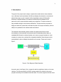
The electronic class schedule system consists of a digital photo frame to show
the schedule, a microcontroller environment used to manipulate picture data, an
embedded WLAN card to retrieve the data, and a server program located on a host
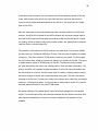
computer to create, store, and send the requested schedules. Several steps must be
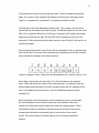
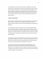
accomplished in order to display the schedule on the screen. These can be seen in
figure 1.
Figure 1: Flow Diagram of Basic Operation.
As can be seen in the figure, first a request is made by selecting a button on the user
interface. The Microcontroller Unit (MCU) system sends a file request to the server
program according to the selection that was made. The server program will then return
2
the requested file, and the MCU system will write that file to a Secure Digital Memory
(SD) card that is shared by the digital photo frame. The digital photo frame can then,
in normal operation, read the SD card and display the schedule as a picture to the user.
The digital photo frame, being the only limitation of the project, was used because it is
inexpensive compared to many embedded electronics design screens available for
purchase as kits.
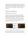
2 Digital Photo Frame and Memory Type
2.1 Digital Photo Frame General Operation
The digital photo frame was chosen as the display for the project because of its
inexpensive cost. Displays commonly sold for embedded projects are expensive and
would make the cost of the electronic picture frame unreasonable. The digital photo
frame can be purchased at Clas Ohlson, a known hardware chain store, and the
price is between 35 and 45 Euros depending on which store branch it is purchased
from. There are also several other models from differing stores that would suit the
project. The only requirement is that they have an SD card interface. The Digital
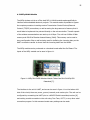
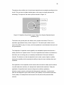
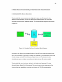
photo frame chosen for this project is shown in figure 2.
Figure 2: User Controls of Digital Picture Frame.
The buttons on the back, shown in figure 2, consist of a Menu button, Directional
buttons, and a Power/Reset button. These are used to set the display characteristics
of the frame. Once set, the unit will display the pictures automatically. The unit has a
3
seven inch screen and wide screen capability. The resolution of the unit is high, as
the resolution is 800 x 480 or 16:10. The frame itself can be placed in the horizontal
or vertical position. It includes a rotatable leg on the back to hold it up and give it
the appearance of a traditional picture frame. It can be purchased with the choice
of a black or white body color. The side of the digital photo frame has three
interfaces which consist of a power adaptor port, Universal Serial Bus (USB) port,
and an SD port that can also take a Multi Media Card (MMC) or a Secure Digital High
Capacity (SDHC) memory card.
To use the digital photo frame a memory card must be inserted into either the USB
port or the SD card port. The unit then reads the memory card for any existing picture
files. After it gathers a list, it will automatically develop a slideshow and begin to
display the pictures. The default setting shows each picture for three seconds with a
transition to the next picture. Once finished with the slide show, the cycle of pictures
will start over.
In the menu the user is able to see which pictures are in which files. Manually
displaying pictures can be done by choosing the picture with the directional button and
selecting it. The menu also gives system settings that can be configured. There is a
calendar setting which allows the user to pick certain photos to be shown on certain
dates. Time and date, as well as time format can all be changed within the settings.
The user is also given the language choices of English, Swedish, Finnish, or Norwegian.
Among the visual settings the user is able to set the unit to display horizontally or
vertically. The possibility of showing up to four pictures at a time is given. The photos
can be changed to show in mono or color. They can also be stretched or configured to
show for the best quality. The screen can be fully configured with controls over
contrast, brightness, saturation, and tint. In addition, the user is also able to control
the type of transition that the pictures use during the viewing of a slide show.
4
2.2 SD Card File System
The SD memory card is a flash memory card which was originally designed to be used
with audio and video devices as higher speeds and higher storage became necessary.
Within the SD memory card there is a microcontroller that is designed to work directly
with the flash memory chips. This microcontroller keeps current information on the
internal workings of the SD card, as well as provides an interface for the user to the
flash chips. Voltage levels for SD cards from different companies may vary. The
common voltage range is 3.3 volts which works well with most microcontrollers. The
communication format and pin configuration of an SD memory card is that of a simple
SPI connection. The SPI pins consist of Slave Select (SS), Serial Data Clock (SCK),
Master In Slave Out (MISO), Master Out Slave In (MOSI), voltage at the Common
Collector (Vcc), and Ground (Gnd). This is a common SPI interface found with most
microcontrollers. There are also additional data lines that can be used if the designer
desires to use the SD bus format of communication. Although higher data rates can
be attained, the programming for this format of communication proves to take more
memory and more processor use than the SPI connection.
The SD card is designed to be able to allow hot insertion. This is when an SD card can
be inserted into the host device, while the device is on, without creating any problems.
This is accomplished by a hardwired connection that is made by pin connectors when
the card is inserted. The host device will see the signal and know to start
communication with the card.
The memory organization of an SD card can be formatted as FAT 16, FAT 32, or
exFAT. In the FAT 16 format the memory is divided up into groups of 512 byte
sections called sectors. These sectors are then organized in groups called clusters. The
number of sectors per cluster can vary with card size. As an example a 2 GB memory
card may have 64 sectors per cluster. These sectors can be used to store data that
can be erased and rewritten frequently. Although most memory is used for raw data,
there are sectors which maintain the file system of the card that must not be
tampered with in order to maintain proper card operation.
5
The first sector, the Master Boot Record (MBR), is reserved and contains the partition
table and other vital information concerning how the memory is organized. It reserves
the entire first sector of the card and typically includes information such as bytes per
sector, sectors per cluster, reserved sectors, File Allocation Table (FAT) entries,
number of root entries, and number of small sectors. This sector, too, is written only
by the internal microcontroller as it keeps the organization of the card. Writing to this
sector using the SPI interface will cause errors and possibly disable the card from
working altogether.
The next sector is the first FAT. In this area there are different entries for each file
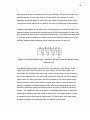
which show how many clusters are used for that particular file. In figure 3 it can be
seen that offset 400 is the beginning of the file allocation table in sector 2.
Figure 3: Screenshot of File Allocation Table Using HxD Hex Editor. Screenshot [1].
Each cluster here is represented by two bytes. As can be seen in the figure, there are
ten clusters available for this specific file. The FAT entry shown starts with the byte
0xF8 and ends with the byte 0xFF. This is kept for the purpose of referencing the size
of the file. The FAT 16 format also needs an exact copy of this file allocation table in a
second FAT entry on the disk for data safety reasons. In the case of data corruption on
one entry, the second is still intact and can be used by the host device. The location of
the second FAT entry can vary depending on the size and make of the card.
6
The next critical section of the memory is the root directory. This contains different
entries, each 32 bytes long, for each file stored in memory. Figure 4 shows a root
directory with one file.
Figure 4: Screenshot of Root Directory Table Using HxD Hex Editor. Screenshot [1].
Shown in the file are examples of information given in the directory section. A total list
of given information includes file name, file type, creation time, last accessed time,
modified time, file cluster, and file size in bytes. This data allows the user to find all the
information about the file and allows the host device to find the raw data in the
memory. The first cluster gives the starting position of the file, and the file size allows
the end of the file to be found.
The last section of the FAT 16 format is the volume boot record. This section is used to
store the raw data of the file. The read and write function will work with a continuous
stream of data in or out but must be moved in chunks of 512 bytes as the SD card
uses responses to ensure data was transferred correctly.
When these entries are properly written to the SD card memory, the file can then be
read by a computer’s operating system or similar devices such as the electronic picture
frame used as the display for this project. [2.]
7
2.3 SD Card Command Format
There are two different modes of communication through the data lines of the SD
memory card. The usual method used by host devices is the SD Bus mode, also called
the SD mode. The other method is the SPI mode. Both modes have similar protocols
but the SD mode allows for multiple data lines operating simultaneously. The SPI
mode is slower than the SD mode but it is easier to implement and it is a well known
interface.
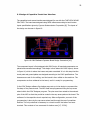
The commands for using the SPI mode of the SD card consist of six bytes which give
the SD card the information it needs to perform the required task. In figure 5 the
command 0, which is used to initialize the card into the SPI mode, can be seen as given
by the PSoC microcontroller over SPI connection.
Figure 5: PSoC Designer SPI CMD 0. Screenshot [3].
The first byte, called the command byte, is made by converting the command number
from a decimal value to a hex value and then adding a hex value of 0x40. Figure 5
shows a command number of 0 added to 0x40 which would give an argument of
0x40. Another example could be the command 55. First the command number 55
would be changed to a hex 0x37 and then added to a hex 0x40 to give a command
byte of 0x77.
8
The following four bytes in the command are 0x00. These are called the argument
bytes. For a read or write operation the address would be given with these bytes.
There is no argument for a command 0, so these are all given as 0x00.
The final byte is the Cyclic Redundancy Check (CRC). This is used by the SD card to
ensure that the information was read correctly. The default setting for the use of the
CRC is off, so while the SD card is in SPI mode, it ignores all CRC values, and dummy
bytes such as 0x95 can be used. The only CRC that is necessary to give is for the
command 0. After the dummy clock pulses are sent to the SD card, it will wait for an
incoming command.
Every full command issued to the SD card will be responded to with a response token
from the SD card. This shows if the command was received and carried out correctly.
Figure 6 shows the makeup of the token response.
Figure 6: Response Token. Taken from SD Specifications Part 1 Version 2.00 [4, 111].
As the figure shows there are three bits, S1 to S3, that make up the response
token. These bits show the results of the command given. For example, there are
three possible response tokens for a write operation which are 101 indicating a CRC
error, 110 indicating a data write error, and 010 indicating the data has been
accepted. [5.]
Many commands need to be issued in order to determine how to proceed with
the communications of the SD card as there are many different makes and
models of SD cards that should be able to be used in the same systems. These
commands are used for example to ensure the card is working at the correct
voltage level and that the commands given to the card are in the correct
format. This process alone could easily take up a lot of the microcontroller's
memory.
9
The additional commands that are needed to distinguish which kind of card has been
inserted can be seen in figure 7.
Figure 7: SD Card Initialization Flowchart. Taken from SD Specifications Part 1 Version
2.00 [4, 16].
The flowchart in figure 7 can be programmed into the MCU unit to automatically
distinguish the card type during the initialization of the SD card. After this is
accomplished, normal operation can be followed until power has been taken away from
the SD card.
10
3 Cypress Programmable System on a Chip
3.1 PSoC Overview
The Programmable System on a Chip (PSoC) microcontroller is a very flexible addition
to the microcontroller world. Its processor is of Harvard architecture and can run
up to 24 MHz. The MCUs can have up to 16 KB of flash memory and 512 bytes of
SRAM. Possible number of I/O ports can be up to 44 depending on which processor
type is purchased. The microcontrollers include internal Analogue to Digital Converters
(ADC), Digital to Analogue Converters (DAC), filters, timers, counters, digital
communication ports, and other functional capability at the disposal of the user. When
configuring the program for the PSoC, the user is asked to identify which processor
type is being used so that the PSoC design software may tailor the programming
environment specifically for that PSoC. [6, 25-42.]
3.2 PSoC Functionality
The PSoC has what are referred to as digital and analogue blocks. These blocks can be
programmed to represent any digital or analogue electrical component that is given as
an option in the design software. Every PSoC MCU has a different virtual layout within
the PSoC Designer software, and the number of digital and analogue blocks may differ
with different PSoC MCU types.
Of the digital block type there are digital building blocks and digital communication
blocks. Each is tailored slightly different for multiple needs. For example if a Serial
Peripheral Interface (SPI) or Universal Asynchronous Receiver/Transmitter (UART)
connection is needed when the user selects the module to be placed, only the digital
communication blocks will be used. Within the analogue blocks there are continuous
time blocks and switch capacitor blocks. These too are designed differently to
serve different purposes. The continuous time blocks are built of operational amplifier
configurations, while the switch capacitor blocks are composed of capacitors that are
switched to achieve the desired result.
11
Figure 8 shows the layout of these analogue and digital blocks and the basic
structuring that the designer has to work with.
Figure 8: PSoC Designer Digital and Analogue Blocks. Screenshot [3].
As figure 8 shows these blocks, once placed, can then be interconnected with visual
routing. All busses that are available for use are visible as well as external pins that
might need to be accessed by the user. If several inputs were to be multiplexed into a
single block, this could be achieved through the visual routing and configuration of
the PSoC Designer software. However, bus comparators are also available for logical
operations of inputs or outputs.
Each block will also give available options for the clock inputs. These can be set to the
system clock, a divider of the system clock, a pulse width modulator, or an external
clock input. With each block there also comes a set of parameters that can be
configured. For example, an SPI Master block will allow the user to set which pins are
used for SS, MISO, MOSI, and SCK. Additionally, it gives the options of which clock to
synchronize to and whether the output should be inverted.
12
Once the blocks are set and the pin routes have been placed, global settings can be
configured. Figure 9 shows the available global settings in the PSoC designer.
Figure 9: Global Settings in PSoC Designer. Screenshot [3].
As can be seen in figure 9, in the global settings the user can set many global controls
of the system, such as the speed of the Central Processing Unit (CPU) clock. The range
of this will differ in various models. The clock divider variables VC1, VC2, and VC3 can
be configured in the case that a lower clock speed is needed for one of the blocks
in the program. The system can be configured to run with three volts or five volts.
The user can set which level they would like the reference voltage to be, as well as
several other options given to better fit the needed parameters of the project.
Once the hardware and Global Settings are prepared, the user can then add further
functionality by the use of the C programming language. Additionally, included
files which are written in assembly can be modified to the user's needs. Many of
the hardware settings that were previously made can be programmed in the
code to change while the microcontroller is in operation. For example, for this
project the digital communications to the SD card needs to be below 400 KHz for
initialization of the card but then sped up to a much faster speed for the data
13
transfer. This is handled within the body of the program code by calling the respective
function and giving the required argument. Exploiting the use of the code can be
beneficial to the user. If for example the user has used all the blocks available and
cannot add external filtering, the implementation of a digital filter written in the C
language can be used in the program. [6, 42-53.]
4 Microcontroller Interfaces
4.1 UART Communication
The UART is an older but still widely used form of digital communication. The physical
connections consist of transmit, receive, and a common ground. The typical speed for
UART communication has always been a baud rate around 9600 bps, although modern
UART connections can be programmed to reach speeds over ten times higher.
The transmission of the data between two modules starts with making sure both have
the same baud rate, as there is no common clock signal for synchronization. The
organization of the data bits is what is used to control data flow. Figure 10 shows the
construction of a UART data packet.
Figure 10: UART Packet Construction.
When the sending unit starts its transmission, it starts the packet with a start bit.
The start bit being a logical low is noticed by the receiver as a signal that information
is coming. The data is then transmitted starting with the least significant bit first.
There is an optional parity bit that can be used. Then the transmission is ended by
the last bit which is a logical high stop bit.
14
The communication can be set up to be full duplex or half duplex. There are also
options that can be exercised such as using a parity bit, character length, and a stop
bit. More modern UART connections, renamed Universal Synchronous/Asynchronous
Receiver/Transmitter (USART), have been designed to utilize clock signals. This gives
them the ability to communicate synchronously or asynchronously, eliminating the
need for start and stop bits. This helps to improve efficiency and the speed of the
data transmission.
4.2 SPI Communication
SPI connections are widely used as well these days though they are not as old as the
UART connections. The SPI connection consists of SS, MISO, MOSI, and SCK. The
speed of the SPI connection can be set for many MHz depending on the device that is
being used.
The communication of the data of the SPI connection is a full duplex shift register
system. The data is written to the register of the unit and then clocked out to the
register of the receiving unit. As the names suggest, MOSI is for the data coming from
the master to the slave and MISO is for the data coming from the slave to the master.
The registers used are usually 8 bits in length. Both sides are synchronized with the
same clock signal.
Several options are given for the SPI connection. One option is the clock polarity. This
sets whether the system sees a logical 1 or a logical 0 as the base value for the clock
signal. Also there is the clock phase. This dictates whether the register will read or
write data on the raising edge or the falling edge of the clock pulse.
The SPI connection also gives the advantage of having multiple slaves. In this
configuration the slaves all share the same MISO, MOSI, and SCK lines but have
different SS lines. A single slave unit can be singled out by holding its slave select line
to a logical 1. As the other slave’s SS lines are held to a logical 0, they will not listen to
the communications on the common lines.
15
4.3 WiFly WLAN Module
The WiFly wireless unit is an off the shelf 802.11 WLAN module made specifically to
interface with embedded electronic projects. This module makes it possible to bypass
the complex procedure in making custom Transmission Control Protocol/Internet
Protocol (TCP/IP) connections, as well as saving the large amount of memory that it
would take to implement the protocol directly on the microcontroller. Transfer speeds
of the wireless communication can reach up to 4 Mbps. The unit has 8 Mbits of flash
memory and 128 KB of Random Access Memory (RAM). This memory can be used to
store configuration files as well as being used for buffering the incoming data, as the
UART connection transfer is slower than the incoming data from the WLAN.
The WiFly module can be purchased on a breakout board called the Surf Board. The
layout of the WiFly module can be seen in figure 11.
Figure 11: WiFly RN-131GSX Wireless Module. Taken from RN-134 WiFly GSX
Datasheet [7].
The interface to the unit is UART, and as can be seen in figure 11 on the bottom left
side of the circuit, there are power, ground, transmit, and receive pins. The unit can be
configured by connecting the UART pins to a HIN232 Serial transmitter/receiver [8]
and making a serial connection to the unit using Tera Term, PuTTY, or any other serial
connection program. In this command mode many settings can be made.
16
Once the WiFly unit is setup it can be taken out of command mode. Any further system
changes can be made via a TCP/IP telnet session, given that the user knows the IP
address of the WiFly unit [9].
In command mode there are many options the user can configure to suit the project's
needs. There are options to use User Datagram Protocol (UDP) or TCP/IP protocols.
There are data transfer rates that can be changed, along with buffer size and packet
terminator characters to make custom size packets. There are a lot of useful features
that make this device an easy solution to embedded wireless networking.
The WiFly unit has external pins for sensor implementation. This is useful when the
designer wants to have the WiFly unit broadcast data upon a sensor trigger
sequence. The external pins can also be used to initiate sleep or to wake the module.
Automatic commands can also be configured such as configuring the WiFly unit to
obtain an IP address upon power up. Another example could be the automatic
writing of bytes to the UART connection when a task is completed or a sensor has
been triggered.
4.4 Capacitive Touch
Capacitive touch sensing technology works on the concept that a change in the
capacity of a button type interface results in a change of a signal that is being
monitored. The button type interfaces can range from simple buttons and slide bars to
large touch screens that track the location of where the user’s finger is on the surface.
All of these examples use the same method of detection. When the capacitance change
alters the signal, the change in the signal is recognized by the system and can then be
used to trigger specific actions in the system.
The skin of the finger acts partially as a dielectric and partially as a conductor which
interacts with surrounding electric fields. The electrolytes within the fingers also
interact with the electric fields. As the finger touches the area of the capacitive touch
sensor, this interaction with the electric fields is what changes the capacitance. The
finger and the body physically become part of the capacitance of the system, adding to
the existing capacitance of the circuit. This change in capacitance then modifies the
17
parameters of the oscillator circuit which change the speed at which the circuit
oscillates. The oscillation comes from what is known as a Capacitive Sensor Relaxation
Oscillator (CSR). Figure 12 shows the circuit layout of the CSR.
Figure 12: Capacitive Sensor Relaxation Oscillator. Taken from Lesher Todd [10].
The circuit consists of a comparator, a switch, and a capacitance that comes from the
layout of the buttons. The capacitor is first charged to a voltage level defined by the
comparator. When that voltage is reached the switch is closed to allow the capacitor to
discharge into ground. The time that it takes to complete this cycle is noted by the use
of a counter. The cycle is repeated and the counter results are compared to one
another. As the capacitance changes due to a user touching the button, the charge
time will grow larger due to the increase in capacitance. The larger charge time can be
seen in the form of a larger counter number. The MCU is programmed in such a way
that as the charge time of the capacitor passes a preset threshold, predefined actions
are triggered. For example, a relay can be connected that will in turn start a motor or a
large bank of lights. Several of the capacitive touch buttons can be implemented on
the PSoC MCU, acting independently of each other, to perform different operations for
the system [11].
Many of the capacitive touch pads designed in projects are based on printed circuit
board layouts. The design is done in specific software so that proper spacing between
capacitive sections of the button can be attained.
18
The pads are then milled out of circuit board material and connected accordingly to the
circuit. This can then be hidden behind glass or thin paper to visually enhance the
technology. The layout of the sensor pad can be seen in figure 13.
Figure 13: Capacitive Sense Button Layout. Taken from Cypress Capsense layout
guidelines [12].
The button and ground plane are milled onto a printed circuit board. There is a
separation gap between them, shown in figure 13. The sensor pad is taken into an
input of the MCU by way of a trace, and the capacitance is read between the input and
the ground plane.
The integration of capacitive touch capability into embedded systems has become a
widely used form of system control. The use of capacitive touch buttons is attractive in
that there are no moving parts, so necessary maintenance of the user interface is
lowered. The buttons can also be adjusted to work under a pane of glass or plastic,
keeping the usability while increasing the ability to keep the user interface clean and
functional.
One application of the capacitive touch sensors that has become widely used is buttons
on public electronic machines, for example train station ticket machines. Today the
application of capacitive touch sense to things such as kitchen appliances,
television remote controls, and hand held video games is also seen. As some touch
pads can be designed to give multi-functions, the usability of the interfaces becomes
much greater, for example the touch screen of a cell phone with press and slide
controls.
19
5 Microcontroller Environment of the Electronic Class Schedule
5.1 Functional Division of Microcontrollers
In this project two types of PSoC MCUs were used due to the fact that the MCU
needed for the capacitive touch sensing did not have enough digital blocks to manage
both the capacitive touch and the communication functionality. For the duration of this
thesis work they will be referred to as the Control MCU and the Communications MCU.
The PSoC microcontroller used for the Control MCU is a CY8C21534. This PSoC was
chosen to take care of the capacitive touch buttons and the management of power for
the digital photo frame and the Communications MCU. This processor type works with
a settings wizard in the PSoC Designer software that creates capacitive touch pad
settings for the user. For the management of power in the system, this model has
enough I/O pins to use it to gate several transistors for power flow control in critical
areas. It has a processor speed of 24 MHz and operates from 2.4 volts to 5.25 volts. It
contains 8 KB of flash memory and 512 bytes of static random access memory. This
module provides the normal PSoC function blocks such as Pulse Width Modulators
(PWM), ADCs, counters, timers, UART, and SPI. It also has the option to utilize up to
20 of the input/output ports as capacitive sensing and proximity sensing. [13.]
The Communications MCU is a PSoC type CY8C29466. The capability of this
microcontroller to have up to 16 digital blocks is why it was chosen to control the WiFly
and SD card communications. It has a processor speed of 24 MHz, 32 KB of flash
memory, and 2 KB of static random access memory. It can have 12 analogue inputs,
four analogue outputs, or up to 44 digital input/output ports. [14.]
20
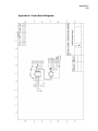
The system has been designed to have several sections of the unit function in a
specific order. Every time the electronic class schedule is used, the unit follows the
same function flow which is shown in figure 14.
Figure 14: System Sequence Block Diagram.
As can be seen in the figure, when a user touches a button, the Control MCU sends a
logic 1 on the signal line that signifies the user’s button press. The Control MCU then
turns on power, by way of block 1, to the Communications MCU. This is accomplished
by the use of a transistor set which is designed to allow enough current for the
operation. The block 2 route is held off in this phase. Once the Communications MCU
is on, it turns on power to the WiFly WLAN unit and sends a logic 1 to the enable
switch so that it may write to the SD card. After data is sent from the electronic class
schedule’s Network File Server (NFS) and written to the SD card, the Communications
MCU sends a write finished signal to the Control MCU. The Control MCU then cuts
power to route 1 effectively turning off the Communications MCU, the WiFly WLAN,
and the enable write signal. It then gives power to route 2, by use of another
transistor set, turning on the electronic picture frame and the enable read signal so
21
that the picture frame may access the file on the SD card. The picture is shown for a
specified amount of time after which the Control MCU will cut power to route 2
effectively turning off power to the enable read signal and electronic picture frame.
The process can be initiated at any time by the user by pressing one of the buttons.
The alternate enabling of the data lines is implemented due to the fact that both the
electronic picture frame and the Communications MCU are both master SPI units, and
they conflict with each other if connected simultaneously. The method that was found
to work the best to isolate which master was to use the SD card was the use of the
HEF4066 bilateral switch integrated circuit which can be seen in figure 15.
Figure 15: HEF4066 Bilateral Switch. Taken from HEF4066 Quadruple bilateral switch
Datasheet [15].
The HEF4066 bilateral switch consists of four logic switches as can be seen in the
figure. Each logic switch consists of an input, output, and an enable signal. For
this project two HEF4066 chips were used, one for the connection of the SD card to
the Communications MCU, and one for the connection of the SD card to the digital
photo frame. For writing purposes, the MCU is allowed to turn on its enable signal
giving it access to the SD card while the digital photo frame is held off. When the
writing is complete, the Communications MCU turns off its enable signal and loses
its power, effectively holding the enable signal to a logical 0 through a pull down
resistor. The Control MCU then gives power to the digital photo frame as well as its
enable signal allowing the photo frame to read the file. The switch requires 5 volts
to operate but can switch and be enabled with 3.3 volts making it an ideal choice
for the low voltage communications that are present in this project.
22
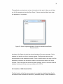
5.2 Design of Capacitive Touch User Interface
The capacitive touch sense interface was designed for use with the CY8C21534-24PVXI
PSoC MCU. The board was designed using PADS software according to touch button
layout specifications given by Cypress Semiconductor Corporation [8]. The layout of
the design can be seen in figure 16.
Figure 16: PADS Software Capsense Board Design. Screenshot [16].
The component layout is first designed with PADS Logic. All required components are
placed and connected accordingly. This design is then taken into PADS Layout, shown
in figure 16, which is where the traces and pads are added. It is in this step that the
touch pads and ground plates are designed according to the PSoC specifications. The
clearances are set for the milling, and the board is then milled on the machine. The
components are then soldered to the board, and it is ready for programming.
In the PSoC Design software five buttons were set up in the design to represent the
five days of the present week. The MCU itself was programmed using the cap sense
wizard within the PSoC Designer program. The pins were then routed to the external
pins of the MCU so that they could be routed to the cap sense pads on the board. The
software for the capacitive touch required very little configuration, as most of the
programming is done by the cap sense wizard and through the use of prewritten
libraries. The only code that is necessary is a check to see if the button has been
touched. This consists of one command for button scan [17, 35-36].
23
5.3 Interfacing WLAN Module
The interfacing of the WiFly module involved both hardware and software
configuration. An external antenna was purchased for use with the Wifly unit, to give a
boost of 2 decibels (dB) to the antenna system. The range of the internal antenna
proved to be too weak for reliable communications. The physical connection to the
WiFly unit is a common UART connection. The connections were taken to the pins of
the Communications MCU via a set of manual switches providing easy system
programming capabilities. Figure 17 shows the connection of the manual switches.
Figure 17: Manual Switching of WiFly Connections.
As can be seen in figure 17, the power and data lines can be isolated from the
Communications PSoC and directed to the Serial to UART adaptor HIN232 [8]. This is
to alleviate any communication problems while programming the WiFly unit via its
serial connection, as a simultaneous connection of the data lines to the
Communications MCU might alter the data during transfer.
The software configuration of the WiFly unit is done by establishing a connection with
a serial communications program on the computer such as Putty or Tera Term. The set
comm open command was set to transmit a byte representing the letter O out of the
UART connection to the Communications MCU when a TCP/IP connection was
established. This is to tell the MCU that the connection has been made and it can start
24
sending commands for delivery to the NFS. Dynamic Host Configuration Protocol
(DHCP) was turned on so that the unit would automatically get any available IP
address from the wireless network. The IP protocol was set to auto connect on power
so that no command was needed from the MCU. The WiFly unit will be powered off
when not in use so auto-connect on power up was a viable option. The UART
communication parameters were set to 14400 baud rate with no parity bit. In
addition, the appropriate security parameters were set so that the WiFly unit could
establish a connection on the secured wireless network. There are many other
parameters that can be set for use with the WiFly, but these were the only
parameters which were needed for this project.
The setup of the Communications MCU required only the connection of the WiFly UART
terminals to the MCU pins and internal routing and programming of the MCU. Using
PSoC Designer, the pins were routed to a UART communications block. The clock for
the UART block was set to use the clock divider selection of VC3. The main clock signal
being 24 MHz is divided by a VC1 value of 2 and then divided by the VC3 value of 104.
The UART block then again divides the clock signal by eight to find its baud rate. This
was calculated to be 14423 which is within the clock tolerance to a 14400 baud rate.
Clock synchronisation of the UART communications block was set to Sync to SysClk for
best synchronisation at this speed.
The programming for the use of the UART was done in the C language in PSoC
Designer. The code was written to read which button was pressed from the Control
MCU, and then it was necessary to wait for the incoming letter O from the UART
connection signalling that that WiFly has established a TCP/IP connection. When this is
received, the program will send out a file name corresponding to the button that the
user has pressed. For the initial project the names of the files were given as file1 to
file5 representing the five days of the week. The program then waits for incoming file
size and sector count data to be delivered via the UART connection. The directory
entries for the FAT file system are prewritten in a character array, and the file size data
is used to modify the directory entry to reflect the correct file size for the file that is
being retrieved. After the array has been modified the MCU then sends out a letter S
as a start byte to signal that it is ready for the raw data. The raw data is sent to the
25
WiFly and buffered as it is sent out of the UART connection. The MCU is
programmed to enter this raw data directly to the SD card in 512 byte chunks
using a FOR loop. The sector count that was received from the server program
dictates the length of this loop for proper writing function. After all of the data is
received from the UART connection the WiFly unit is no longer needed, and it is
powered off by the Communications MCU.
5.4 Integration of SD Card
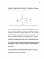
For the connection to the SD card the Communications MCU was used. The pins of the
SD card can be connected to the pins of the MCU and used in SPI mode. Figure 18
shows the correct connection of the SD card to the PSoC microcontroller.
33 .V
33 .V
1k 1k 1k 000
S C rdS cke
Da
ot
S_ E2 DR S
S C rd Da
9
S_S DC
1
S_S DC
S _ OI DM S
S
2
S _ OI DM
VS S
3
VC C
4
5
S _ CK DS L
L
S_ E1 DR S
S_ P DW
33 .V
6
VS S
S _ IS DM O
O
CM O
S _ CK DS
7
S _ IS DM
8
S_D DC
S_D DC
S_ P DW
Figure 18: SD Card Interface to PSoC Microcontroller. Taken from PSoC SD Card
Module Solution PPT [18, 14].
The SD card socket shown in figure 18 can be a purchased prefabricated SD card
breakout board, or as in this project it can be a custom breakout board made from a
Micro SD to SD card size adaptor with pin connectors soldered to the contacts. The
SD_CD and SD_WP pins were not utilized in this project as they are for functions that
were not needed for the operation of the electronic class schedule. The four data lines
26
MISO, MOSI, SCLK, and SS were not taken directly from the SD card to the MCU as
shown in the figure but rather switched through the HEF4066 bilateral switch
integrated circuit [15]. Only during the time of reading the file for display will the
enable signal to the HEF4066 and the power to the digital photo frame be turned on.
This allows the photo frame, upon power up, to read that there is a new file on the SD
card, as well as saving power while the unit is not in use. The circuit board for these
connections to the Communications MCU were fabricated using PADS Logic and PADS
Layout in the same fashion as the Control MCU circuit board was designed.
Using PSoC designer the SPI connection was setup to communicate over the pins to
which the SD card was connected. The clock of the SPI communications block was set
up to run from an 8 bit Counter Block. This gives the ability to change the speed of the
SPI connection in real time by changing the values of the counter within the program
code. The counter clock is taken from VC1 having a divider of 2. The main clock signal
is 24 MHz which is divided by the VC1 value of 2, then divided by the period value for
the counter which is initialized to 60. When the SPI connection block receives the clock
signal it divides this again by two to find its clock rate. This gives a calculated clock
signal of 100 KHz which is used for the initialization of the SD card. Once the
initialization is finished, the Counter Block is programmed to switch to a period of eight
for a clock speed of 750 KHz. This is the speed that is used for data transfer.
This speed can be taken up to several MHz if needed after the card initialization is
accomplished below a speed of 400 KHz. For stability issues the speed was kept
relatively low for this project. Additionally, the UART baud rate limits the speed of the
data flow, so higher rates on the SPI connection are not necessary.
27
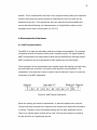
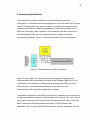
Within the software of the MCU there are two arrays that are used in the writing of
data to the SD card. The first is the FAT entry and the second is the Directory entry.
The arrays can be seen in figure 19.
Figure 19: SD Card File Information Arrays.
Figure 19 shows the information that needs to be written to the SD card so that the file
is recognized as a picture file. The only information that is modified is the size of the
file when the MCU is retrieving information from the server program. It is not
necessary to have a file system erase and create a new file every time, because only
one file is needed for display at a time. This allows the system to use the same file
space repeatedly, verses finding free space every time a write command needs to be
executed. Additionally, the proper use of a filing system on the MCU would require
more memory than is available. Once the file size of the Directory entry has been
modified, the MCU writes the FAT entries and the Directory entries to the SD card. Two
FAT entries are needed for filing system redundancy checks. For the card used on this
project the first FAT entry is in the address space sector 2, the second FAT entry is
in address space sector 241, and the Directory entry is made in sector 480. As the
arrays for these entries are under 512 bytes, and a successful write command needs
512 bytes exactly, the remaining missing bytes are filled in with the hex value 0x00.
Filling the remaining data in a sector with dummy bytes was accomplished with a
FOR loop count of 512 minus the partial raw data in the sector. The Communications
MCU is then ready for the raw file data.
28
As the raw data starts to come in from the wireless unit, a continuous write command
is first issued to the SD card, and data is written directly to the card. The write
command used to make the data write function is similar to the command 0 that was
shown in section 2.3. Figure 20 shows the continuous write command 25 as given via
the SPI to the SD card.
Figure 20: PSoC Designer SPI CMD 25. Screenshot [3].
As can be seen in the figure, the command starts with the command byte of 0x59
representing a continuous write function. Next is the argument which gives the
memory location to be written to, shown here as variables passed to the function. The
CRC is not necessary at this point as the card is initialized and in SPI mode, so once in
SPI mode the hex number 0x95 is used instead as a dummy byte for the CRC.
After the continuous write command, the MCU waits for an accepted response token
from the SD card. Then the MCU is free to send data beginning with the start byte of
0xFC. The SD card knows then that everything following is raw data and should be
saved into the respective memory locations. This is a continuous write command and it
will take data in one sector at a time until a proper stop token is received. This sector
grouping is such that the SD card may perform a CRC on the data with every sector.
This grouping is not avoidable even though the CRC is not being used. Furthermore, this
grouping does slow down the transmission of data. When all data is sent on the
29
continuous write command, the host device must fill the remaining space of the last
sector with dummy bytes of the hex value 0x00 and then send the stop token in
order to receive a data accepted token from the SD card. The stop token is a single
byte of hex 0xFD.
After the stop token is sent and the data has been correctly written to the SD card
memory, the MCU will cut power to the WiFly wireless unit and send a signal back to
the Control MCU that the file has been successfully written to the card and it is ready
for viewing. When all sectors have been properly written, the digital photo frame can
read the file as a normal picture file.
The locations of the entries on the SD card can vary with cards. The SD card utilized
for this project is a Transcend 2GB Micro SD card. This card uses 64 sectors per cluster
of memory. This gives a total of 32768 bytes of memory per cluster. For this project
the FAT entries were written to include the space of 10 clusters for the file. This gives
a usable memory space of 327680 bytes for the file. The Directory entry includes
the card information, file name, size, starting sector, time, and date information. The
array in the MCU only includes enough information to cover the card information and
the information for one file. The file name, date of creation, starting memory sector,
and other aspects of the file can remain the same every time. The only information
changed is the file size. The last entry made is the volume entry where the raw data is
written to. The beginning sector for the raw data is always set to sector 512, and the
reserved space continues for the next 327680 bytes.
No system settings of the digital photo frame have been changed from the default
values. The circuit board of the unit has been enclosed and the buttons and card slots
have become inaccessible, as they are no longer needed for the operation of the
schedule.
30
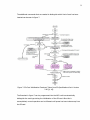
6 Client-Server Functionality of the Electronic Class Schedule
6.1 Schedule File Server Overview
The schedule file server program was designed to serve as a file server for the
electronic class schedules, as well as creating the schedule picture files from data
retrieved from the school schedule website. The functional block diagram can be seen
in figure 21.
Figure 21: Schedule File Server Functional Block Diagram.
As shown in the figure, the proposed function of the NFS is to access the school’s web
server for information to be used in making the schedules. The schedules are then held
in local storage on the NFS until they are ready to be sent. The electronic class
schedules can open a wireless connection and retrieve these files when needed.
The schedule file server has been written in the higher level language C# using
Microsoft Visual Studio 2010 Professional. This was chosen to take advantage of the
form and list box capabilities, as well as the libraries for TCP/IP communication.
31
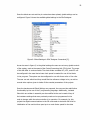
The application was kept basic as the only function at that point in time was to listen
out for file requests and send the files. Figure 22 shows how the listbox looks when
the application is in operation.
Figure 22: Server Program Application Console in Microsoft Visual Studio.
Screenshot [19].
As shown in the figure, the text box shows the status of the server program. In this
example it is listening out for an incoming request. The figure also shows a reset
services button on the application console. This is so that if there is any hang up of the
application, the button can be used to restart all of the services used by the server
program. The list box and form allow the system manager to see in real time what the
program is doing and if there are any problems. [20, 33-37.]
6.2 Creation of JPG Schedule Files
The first function of the file server program is to create the schedule picture files for
the electronic class schedules. It does this by periodically looking up class schedules on
32
the school’s website and parsing information for that particular classroom. It then uses
this data to create a text file version of the schedule and then converts it to a JPG
picture file. Each classroom will have a separate JPG file for each day of the current
week. The program can be set to create files on intervals of every 30 minutes so as to
keep the schedules up to date for display. The JPG files will be stored with names
corresponding to the class number so that upon a request the server program can
easily find and send the correct file. The extent of development of the server program
for this project was given to be delivery of the picture files. The parsing of the
information from the school schedule website will be developed at a further date.
6.3 Connection and Delivery of Schedule Files
The second function of the server program is the delivery of the schedule files.
The program is designed to listen on a particular port for any requests being
made by the electronic class schedules. For the project development, port 2000
was utilized. When a connection is requested, it is accepted and a network
stream is created [20, 172-180]. The listbox at this point will show that a
connection has been made. The electronic class schedule that has made the
request then sends out the name of the file it is requesting. The server program
will scan incoming data and wait until it reads the letter f, as all files that will be
requested will start with the letter f, for example file1. The file name that is
being requested is sent without the file extension. When the file server program
receives the name of the file, it is then added to a prewritten character string.
This string represents the file directory for the file server’s local storage where
the schedule pictures are stored. The extension JPG is then added to the end of
the string and the program uses the string to locate the file. Once the file is
located, a file reader function is opened, and the raw file data can be accessed.
[20, 134.]
When the raw data is opened for access, the size of the file is found and sent back to
the electronic class schedule. The number of 512 byte sectors is then calculated and
sent back. This will be used for SD card writing purposes by the MCU of the electronic
class schedule, as the writing function of the SD card is accomplished in groups of 512
bytes. A note on the listbox is put up showing that the file size has been sent. The
server program then waits for the electronic class schedule to send the hex byte 0x53
33
representing the letter S as a start byte, signifying that it is ready for the raw data.
Once the start byte is received the server program then starts to send the raw data of
the schedule file. When all data has been sent, the connection is terminated and a
message is shown on the listbox that the file has been sent. The server then returns to
the idle mode and shows that it is again listening out for a request.
34
7 Discussion
7.1 Implementation Issues
During this project there were several issues that needed to be overcome, which did
not have simple solutions. These proved to be good learning points and areas
for self development. The first issue was getting the write command to work with
the SD card. The documentation for issuing commands to any SD card is difficult to
find. Every SD card manufacturer has little differences in the way the cards are
communicated with. Furthermore, within each manufacturer’s line of cards there are
different flows of communication depending on what type of card it is and what size
it is. Thus, finding the correct combination of commands takes a great deal of
experimentation. Six different SD cards were used in the development of this project,
and only one was successfully implemented. Also, the Cypress documentation for
using the SD card is rare. The company at one point in time had an SD interface with
libraries that handled the file system, but it was dropped because of too many
unresolved problems and size limitations of the MCUs. When searching the Cypress
forums, few examples showing how to issue byte commands to an SD card can be
found. The main flow of the program came from the SD manufacturer's manual, but
most of the help to resolve the problems came from online forums and hobby
experimenter websites.
Another issue was the fact that the system was developed as a 3.3 volt system to work
with the SD card, negating the possibility to use a Liquid Crystal Display (LCD) with the
microcontroller for debugging purposes. The PSoC MCU is capable of running with 5
volts, and originally it was done so. The SPI data lines to the SD card were taken to
3.3 volts using level shifters. This gave the ability to use the LCD to show the responses
that the SD card was giving. The level shifters were taken out and the MCU
was configured to function on 3.3 volts to help with communication problems between
the MCU and the SD card. The WiFly unit also proved to work better on the lower
voltage. At this voltage the LCD would not work so another temporary MCU was
35
implemented to show outputs on the LCD. A separate SPI connection was programmed
into the Communications MCU and output to the temporary MCU which ran on 5 volts
and had an LCD. This way the whole system could stay at 3.3 volts and the responses
from the SD card could be forwarded and displayed for debugging.
Working with 3.3 volts resulted in problems in switching power to the individual areas
of the system. The transistors used for the switching of power were PNP BC556 [21] and
NPN BC546 [22] used in the Darlington setup to provide better current flow [23, 95].
The rated voltage is 5 volts on both. It was attempted to use these transistors with the
system’s 3.3 volts. The lower voltage did not allow for the proper current and the
switching was intermittent. To solve the problem, the 5 volts from the power supply
was taken into the collectors and switched using the MCUs 3.3 volts on the base. Then
the output was supplied to a MIC5200 voltage regulator [24] which dropped it to
3.3 volts for use in the system.
The largest issue of the project that presented itself was how to properly isolate the
two master SPI connections from each other and give alternate control over the SD
card. The use of the Darlington transistor setup was attempted on each data line but
that idea proved to supply too much stray capacitance and the signals were degraded
so that they would not work. Logic gates were attempted, such as the SN7408, and
the signal still seemed to be degraded beyond a usable amount. Several switching
integrated circuits and multiplexer integrated circuits were used including SN74LS243
transceiver, HCF4053, MM5616 multiplexer, and the HEF4066 quadruple bilateral
switch. All of them gave the same results. The issue was eventually resolved using the
HEF4066. It was found that the problem was a combination of issues. The first issue
being that Vcc on the integrated circuit needed to be 5 volts, though the enable, input,
and output could all be used with the 3 volt system. The second issue was that the
HEF4066 needed to be kept on while the enable pins were held low to effectively stop
a signal. The original method was to cut all power to the HEF4066 and assume that the
36
signals would not pass. This assumption proved to be wrong as it would still degrade
the signal existing in the other switching device. With the HEF4066 left powered up
and the enables held to Gnd when a separation of data lines is required, the system
works as it is supposed to.
7.2 Results
The electronic class schedule performs as it was designed. The user may select one of
five buttons and receive the respective picture file on the screen. Designing the system
to handle larger size picture files could enhance the experience for the user. Though
the existing file size of 3 KB is sufficient to deliver the material, as of now files larger
than 10 KB take too much time to transfer and run a greater risk of losing data. The
system can provide an easy way for teachers to put their schedules to the appropriate
rooms without having to travel around the school changing out paper schedules. This
also includes writing extra comments. For example, if a class is cancelled or moved to
another room, this information can be added to the online schedule for the electronic
class schedule to parse and display for users. There are many other improvements that
future students may add as well to ensure that the electronic class schedule is
developed to its full potential.
7.3 Future Development
The speed of the system was limited by the read and write operations of both the
UART connection to the WiFly and the SPI connection to the SD card. During
development the UART connection was tested to run best at the speed of 14400 bps.
The initialization of the SD card must be below 400 KHz, but it can be stepped up
for data transfer. For this project the data rate was only stepped up to 700 KHz, as the
files are around 3 Kb in size. The total transfer from WiFly to SD card takes a little over
two seconds. Future models of the WiFly unit will include SPI connection, being several
times faster than UART, which will effectively speed up the delivery of data. When
these become available, the speed of the data transfer can be increased enabling the
picture files to be larger and of better quality.
37
Another area of development involving speed is seeing if the Bus mode of the SD card
can be used with the PSoC MCU. Research into using the Bus mode was not done. During
the project this concept was not seen in any other similar SD card embedded projects. If
this can be accomplished, then three data lines would be available for the movement of
data.
The addition of extra memory to the unit could assist in enhancing the user
experience. EEPROM or SRAM external memory could be used to store additional
pictures such as system error messages to the user or special notices pertaining to
that classroom. System messages could also be displayed to the user to show which
file is being retrieve. In addition, directions on how to use the electronic class
schedule could be displayed to the user. Currently the electronic class schedule is
not set up to show anything on the screen until the schedule is received and written
to the SD card.
The ability to send a file directly to the electronic class schedule would be a good
future feature for teachers. This would allow the teachers to send messages showing
that a class has been cancelled or moved to another room. The system as it is only
shows what is put into the class schedules online. To add personal messages, one
would need to be able to wake the unit from the power down state and send a
file for display. Developing a second application that could be given to the
teachers could allow the teachers to directly connect to a specific class schedule
and give it a custom picture file. The addition of the external memory could assist
in implementing this idea, as the message could be stored and shown when a
schedule is not being requested.
One issue that could be corrected in future versions is the incompatibility of SD cards.
During the experimentation there were six SD cards that were used to develop the
initialization and write command. During the end phase of the project only one card
was working properly. This is due to the fact that each card responds differently to the
commands, so there needs to be an initialization process as discussed in section 7.2 to
correctly initialize more than just one type of card. This may very well take a lot of
memory, in which case the Communications MCU would need to be replaced with a
model that has more memory available. With the current MCU designs that are out on
the market today, this notion could be easily achieved.
38
The last area of development is the server program. This program could be developed
further to show all files that have been parsed and turned into JPG files. It could give
information such as size and the time they were created and show a list of the files in
the working program window. The program could also show which electronic class
schedule was connected to it and keep a small log of the communications it has done.
Also the current design only handles one request at a time. The program could be
structured to handle several requests when several units are placed around the school.
39
8 Conclusions
The goal of developing a low priced system that could retrieve class schedules over the
wireless network and present them on a screen for the user was met. A server program
was written that can properly listen out for file requests and return the correct file to
the unit which made the request. The electronic class schedule has been developed to
a point that it can retrieve the picture files over the wireless network and write them
to the SD card for viewing on the electronic picture frame. The system has been
designed with the minimum specifications of the project goal, and it fulfils the
requirements set for it. Given the proper time and research, further development can
be made to upgrade the functionality in the system making the electronic class
schedule a viable option for class schedule delivery.
40
References
1. HxD hex editor [computer program]. Version 1.7.7.0. Saarbrücken, Germany: mhnexus; April 3, 2009.
2. Grover James. SD card map [online]. Akron Ohio, USA: University of Akron.
URL: http://www.ecgf.uakron.edu/grover/web/ee470/labs/SDCardMap.pdf.
Accessed November 12, 2010.
3. PSoC Designer [computer program]. Version 5.1. San Jose California, USA: Cypress
Semiconductor Corporation; December 27, 2010.
4. SD Association. SD Specifications Part 1 Version 2.00 [online].
URL: http://www.sdcard.org/developers/tech/sdcard/pls/Simplified_Physical_Layer_
Spec.pdf.
Accessed November 12, 2010.
5. Maxim. Interfacing SD cards with the TINI system [online].
URL: http://www.maxim-ic.com/app-notes/index.mvp/id/4068.
Accessed October 8, 2010.
6. Ashby Robert. Designer's guide to the Cypress PSoC. Oxford, United Kingdom:
Elsevier; 2005.
7. Roving Networks. RN-134 WiFly GSX datasheet [online]. Los Gatos, California,
USA: Roving Networks.
URL: http://www.rovingnetworks.com/Docs/WiFly-RN-134-DS.pdf
Accessed October 20, 2010.
8. Intersil Americas Inc. HIN232 RS-232 transmitter/receiver datasheet [online].
URL: http://pdf1.alldatasheet.com/datasheet-pdf/view/392674/INTERSIL/
HIN232.html.
Accessed October 19, 2010.
9. Roving Networks. WiFly GSX user manual/command reference [online]. Los Gatos,
California, USA: Roving Networks.
URL: http://www.rovingnetworks.com/documents/WiFlyGSX-um.pdf.
Accessed October 20, 2010.
10. Lesher Todd. Learning about capacitive proximity sensing by building a thermin
[online]. San Jose, California, USA: Cypress Semiconductor Corporation.
URL: http://www.cypress.com/?docID=17301.
Accessed December 18, 2010.
11. Cypress Semiconductor Corporation. Getting started with capsense [online]. San
Jose, California, USA: Cypress Semiconductor Corporation.
URL: http://www.cypress.com/?rID=48787.
Accessed December 19, 2010.
41
12. Cypress Semiconductor Corporation. Capsense layout guidelines [online]. San Jose,
California, USA: Cypress Semiconductor Corporation.
URL: http://www.cypress.com/?docID=2995.
Accessed December 19, 2010.
13. Cypress Semiconductor Corporation. CY8C21534 datasheet [online]. San Jose,
California, USA: Cypress Semiconductor Corporation.
URL: http://www.cypress.com/?rID=3345.
Accessed December 18, 2010.
14. Cypress Semiconductor Corporation. CY8C29466 datasheet [online]. San Jose,
California, USA: Cypress Semiconductor Corporation.
URL: http://www.cypress.com/?rID=3334.
Accessed December 18, 2010.
15. Philips Semiconductors . HEF4066 quadruple bilateral switch datasheet [online].
URL: http://pdf1.alldatasheet.com/datasheetpdf/view/17722/PHILIPS/
HEF4066B.html.
Accessed February 10, 2011.
16. PADS PCB design tools, ES Suite [computer program]. Wilsonville Oregon, USA:
Mentor Graphics Company; December 2010.
17. Cypress Semiconductor Corporation. Capsense Sigma Delta datasheet [online].
San Jose, California, USA: Cypress Semiconductor Corporation.
URL: http://www.cypress.com/?docID=24669.
Accessed December 19, 2010.
18. Cypress Semiconductor Corporation. PSoC SD Card Module Solution PPT [online].
San Jose, California, USA: Cypress Semiconductor Corporation.
URL: http://www.cypress.com/?rID=3424.
Accessed December 19, 2010.
19. Microsoft Visual Studio 1020 Professional [computer program]. Version
10.0.30319.1. Microsoft Corporation; 2010.
20. Allwork John. Visual Studio C# 2010 programming and PC interfacing.
Amersfoort, Netherlands: Elector International Media BV; 2010.
21. Motorola, Inc. BC556 PNP transistor datasheet [online].
URL: http://pdf1.alldatasheet.com/datasheet-pdf/view/11551/ONSEMI/BC556.html.
Accessed February 10, 2011.
22. Motorola, Inc. BC546 NPN transistor datasheet [online].
URL: http://pdf1.alldatasheet.com/datasheet-pdf/view/11550/ONSEMI/BC546.html.
Accessed February 10, 2011.
42
23. Horowitz Paul, Hill Winfield. The art of electronics, second edition.
Cambridge Massachusetts: Cambridge University Press; 2009.
24. Micrel . MIC5200 voltage regulator datasheet [online].
URL: http://pdf1.alldatasheet.com/datasheet-pdf/view/407520/MICREL/MIC52003.3BS.html.
Accessed February 10, 2011.
Appendix 1
1(1)
Microcontroller Specifications
CY8C21534 Cypress
- Clock 24 MHz
- Operating voltage 2.4 V to 5.25 V
- Operating temperature range -40 to 85 Celsius
- 4 analogue blocks
- 4 digital blocks
- 8 KB flash memory
- 512 Bytes SRAM
- Programmable pin configurations
- Programmable multiplexing
- I2C, UART, SPI communications
- Programmable watchdog timers
- Supports Capsense buttons
- 28 analogue inputs
- 0 analogue outputs
- 28 digital I/O ports
CY8C29466 Cypress
- Clock 24 MHz
- Operating voltage 3.0 V to 5.25 V
- Operating temperature range -40 to 85 Celsius
- 12 analogue blocks
- 16 digital blocks
- 32 KB flash memory
- 2 KB SRAM
- Programmable pin configurations
- Programmable multiplexing
- I2C, UART, SPI communications
- Programmable watchdog timers
- 12 analogue inputs
- 4 analogue outputs
- 44 digital I/O ports
Appendix 2
1(15)
Program Code - Communication MCU Program
//------------------------------------------------------------// Metropolia University of Applied Sciences
// Marcel Mushik 24 April 2011
// Final year project - Electronic class schedule
// Code: Control MCU program
//------------------------------------------------------------// Include files ---------------------------------------------#include <m8c.h>
// part specific constants and macros
#include "PSoCAPI.h" // PSoC API definitions for all User Modules
// Global variables ------------------------------------------int i = 0;
int count = 0;
int decision = 0;
// Declarations -------------------------------------#pragma interrupt_handler Timer8_ISR
void button_press(void);
// timerISR to be handled as the interrupt code
// Function description---------------------------------------// Main function. Receives button selection from user.
// Turns on power to Communications MCU and forwards button selection.
// Waits for a signal indicating that data has been downloaded and written to SD
// card.
// Turns off WiFly, and gives power to Digital photo frame, also enables read.
// Times out, or starts again with another button press.
void main(void)
{
M8C_EnableGInt;
// Enables Global interrupts
ButtonSig1_Start();
// Makes ready ButtonSig1 for operation
ButtonSig2_Start();
// Makes ready ButtonSig2 for operation
ButtonSig3_Start();
// Makes ready ButtonSig3 for operation
ButtonSig4_Start();
// Makes ready ButtonSig4 for operation
ButtonSig5_Start();
// Makes ready ButtonSig5 for operation
MCU2_pwr_Start();
// Makes ready MCU2_pwr for operation
SD_pwr_Start();
// Makes ready SD_pwr for operation
Read_enable_Start();
// Makes ready Read_enable for operation
Timer8_WritePeriod(100);
// Sets timer period value
Timer8_WriteCompareValue(0);
// Sets timer compare value
Timer8_EnableInt();
// Enables timer interrupts
while(1)
{
// Reads input from user.
if ((PRT2DR & 0x01) == 0x01)
{
decision = 1;
button_press();
}
else if ((PRT2DR & 0x04) == 0x04)
{
decision = 2;
button_press();
}
else if ((PRT2DR & 0x10) == 0x10)
{
decision = 3;
button_press();
// Button 1 P2.0
// Notes decision
// Forwards decision to function
// Button 1 P2.2
// Notes decision
// Forwards decision to function
// Button 1 P2.4
// Notes decision
// Forwards decision to function
Appendix 2
2(15)
}
else if ((PRT2DR & 0x40) == 0x40)
{
decision = 4;
button_press();
}
else if ((PRT0DR & 0x01) == 0x01)
{
decision = 5;
button_press();
}
}
}
// Button 1 P2.6
// Notes decision
// Forwards decision to function
// Button 1 P0.0
// Notes decision
// Forwards decision to function
if(count == 30)
{
Timer8_Stop();
Read_enable_Switch(0);
SD_pwr_Switch(0);
count = 0;
}
// If timer has interrupted 30 times,
// Photo frame is turned off,
// Resets
// Resets
// Resets
// Resets
ButtonSig1_Switch(0);
ButtonSig2_Switch(0);
ButtonSig3_Switch(0);
ButtonSig4_Switch(0);
ButtonSig5_Switch(0);
//
//
//
//
//
Button
Button
Button
Button
Button
signals
signals
signals
signals
signals
zeroed
zeroed
zeroed
zeroed
zeroed
after
after
after
after
after
forwarding
forwarding
forwarding
forwarding
forwarding
// Function description---------------------------------------// Function takes decision value and forwards the respective button
// signal to the communications MCU.
// All values are reset in case of a new button push.
// Delays are set to give proper warm up time of MCU
// While loop waits until the finished signal is given from the
// communications MCU, in which case it is shut off and power
// and read enable is given to the photo frame.
// The timer is also started for use of its interrupt.
// This creates the timeout before the screen turn off automatically.
void button_press(void)
{
Timer8_Stop();
// Resets
SD_pwr_Switch(0);
// Resets
Read_enable_Switch(0);
// Resets
count = 0;
// Resets
for(i=0; i < 21000; i++); // Delay waits for photo frame to give up control of SD
MCU2_pwr_Switch(1);
// Communications MCU turned on
for(i=0; i < 800; i++);
// Delay for MCU2 warmup
// Sending button signal
if (decision == 1) ButtonSig1_Switch(1);
else if (decision == 2) ButtonSig2_Switch(1);
else if (decision == 3) ButtonSig3_Switch(1);
else if (decision == 4) ButtonSig4_Switch(1);
else if (decision == 5) ButtonSig5_Switch(1);
for(i=0; i < 800; i++);
while((PRT1DR & 0x08) == 0x00);
MCU2_pwr_Switch(0);
Read_enable_Switch(1);
// Delay for read of signal
// Waits for MCU2 finished signal
// Turns off Communications MCU
// Turns on read enable
Appendix 2
3(15)
}
SD_pwr_Switch(1);
Timer8_Start();
// Turns on digital photo frame
// Function description---------------------------------------// Timer which keeps count of timer interrupts.
// Creates time before the photo frame automatically turns off.
void Timer8_ISR(void)
{
count++;
}
Appendix 2
4(15)
Program Code - Communication MCU Program
//------------------------------------------------------------// Metropolia University of Applied Sciences
// Marcel Mushik 24 April 2011
// Final year project - Electronic class schedule
// Code: Communication MCU program
//------------------------------------------------------------// Include files ---------------------------------------------#include <m8c.h>
// part specific constants and macros
#include "PSoCAPI.h" // PSoC API definitions for all User Modules
#include <stdlib.h>
// Global variables ------------------------------------------int i = 0; int j = 0;
int k = 0;
int size;
int file_size = 512;
int file_size_partial;
int sectors = 0;
BYTE Rdata = 0xAC;
BYTE file[5] = {0x66, 0x69, 0x6C, 0x65, 0x31};
BYTE number_of_sectors[2];
BYTE data_size[3];
BYTE fat[20] = {0xF8, 0xFF, 0xFF, 0x7F, 0x03, 0x00, 0x04, 0x00, 0x05, 0x00, 0x06, 0x00, 0x07, 0x00,
0x08, 0x00, 0x09, 0x00, 0xFF, 0xFF};
BYTE directory[64] = {0x54, 0x48, 0x45, 0x53, 0x49, 0x53, 0x20, 0x20, 0x20, 0x20, 0x20, 0x08, 0x00,
0x00, 0x00, 0x00, 0x00, 0x00, 0x00, 0x00, 0x00, 0x00, 0x72, 0x86, 0x9E, 0x3D, 0x00, 0x00, 0x00, 0x00,
0x00, 0x00, 0x46, 0x49, 0x4C, 0x45, 0x20, 0x20, 0x20, 0x20, 0x4A, 0x50, 0x47, 0x20, 0x18, 0x30, 0xA9,
0x86, 0x9E, 0x3D, 0x9E, 0x3D, 0x00, 0x00, 0x9A, 0x92, 0x66, 0x3D, 0x02, 0x00, 0x25, 0x03, 0x00,
0x00};
// Declarations -------------------------------------void card_initialize(void);
void CS_toggle(void);
void write_data_init(BYTE, BYTE, BYTE, BYTE);
void write_data_raw(BYTE);
void write_data_fill(int);
void write_CRC(void); void
stop_token(void); void
start_token(void);
void debug(BYTE);
// Function description---------------------------------------// Main function. Receives button selection from Control MCU.
// Opens connection with WiFly, sends request. //
Recieves data and writes file to SD card.
void main(void)
{
M8C_EnableGInt;
SD_SS_Start();
SD_SS_Switch(1);
Debug_SS_Start();
Debug_SS_Switch(1);
MCU_fin_sig_Start();
MCU_fin_sig_Switch(0);
WiFly_pwr_Start();
//
//
//
//
//
//
//
//
Enables global interrupts
Makes ready SD_SS for operation
Sets SD_SS high, not enabled
Makes ready Debug_SS for operation
Sets Debug_SS high, not enabled
Makes ready MCU_fin_sig for operation
Sets MCU_fin_sig low, not finished
Makes ready WiFly_pwr for operation
Appendix 2
5(15)
Write_enable_Start();
// Makes ready Write_enable for operation
Loading_LED_Start();
// Makes ready Loading_LED for operation
Counter8_WritePeriod(0x60);
// Sets period to 60 clocks
Counter8_WriteCompareValue(0x30);
// Generates a 50% duty cycle
Counter8_Start();
// Starts counter //
UART_Start(UART_PARITY_NONE);
Enables UART
SPIM_Start(SPIM_SPIM_MODE_0 | SPIM_SPIM_MSB_FIRST); // Sets SD SPI parameters
SPIM2_Start(SPIM2_SPIM_MODE_0 | SPIM2_SPIM_MSB_FIRST);// Sets Debug SPI parameters
while(1)
{
// Waits for button press
if ((PRT2DR & 0x04) == 0x04)
{
file[4] = 0x31;
k = 1;
}
else if ((PRT2DR & 0x10) == 0x10)
{
file[4] = 0x32;
k = 1;
}
else if ((PRT2DR & 0x40) == 0x40)
{
file[4] = 0x33;
k = 1;
}
else if ((PRT0DR & 0x01) == 0x01)
{
file[4] = 0x34;
k = 1;
}
else if ((PRT0DR & 0x04) == 0x04)
{
file[4] = 0x35;
k = 1;
}
if(k == 1)
{
WiFly_pwr_Switch(1);
Write_enable_Switch(1);
Loading_LED_Switch(1);
// Button P2.2
// Changes file number to 1
// Button P2.4
// Changes file number to 2
// Button P2.6
// Changes file number to 3
// Button P0.0
// Changes file number to 4
// Button P0.2
// Changes file number to 5
// Turns on WiFly power
// Enables writing to SD card
// Turns on LED to show operational status
// Waits for incoming byte of 'O' to show WyFly has made a connection
while(UART_cReadChar() != 0x4F);
// Catches extra 'O' bytes that are sent by WiFly.
while(UART_bReadRxData() == 0x4F);
// Sends request for file
for(i=0; i<5; i++)
{
}
UART_PutChar(file[i]);
Appendix 2
6(15)
while(UART_cReadChar() == 0x00);
// Scans for valid data
data_size[0] = UART_bReadRxData();
// Stores Lowest byte of
// file size
data_size[1] = UART_cGetChar(); // Stores middle byte of file size
data_size[2] = UART_cGetChar(); // Stores highest byte of file size
// Find number of bytes left after all 512 size writes will be made
file_size_partial = ((data_size[1]<<8)|data_size[0]) + 1;
while(file_size_partial > 512) file_size_partial = file_size_partial - 512;
file_size = file_size_partial;
// Writes file size to directory entry string
directory[60] = data_size[0];
directory[61] = data_size[1];
directory[62] = data_size[2];
// Gets number of sectors for proper future loop counts
while(UART_cReadChar() == 0x00);
number_of_sectors[0] = UART_bReadRxData();
number_of_sectors[1] = UART_cGetChar();
sectors = ((number_of_sectors[1]<<8)|number_of_sectors[0]) - 1;
card_initialize();
// SD card initialization into SPI mode
Counter8_WritePeriod(0x30);
// Sets period to 30 clocks
Counter8_WriteCompareValue(0x15); // Generates a 50% duty cycle
write_data_init(0x00, 0x00, 0x04, 0x00);
// Writes first FAT entry
start_token();
// Address sector 2, offset 400
for(i=0;i<sizeof(fat);i++)
{
write_data_raw(fat[i])
;
}
write_data_fill(sizeof(fat));
write_CRC();
stop_token();
write_data_init(0x00, 0x01, 0xE2, 0x00);
// Writes second FAT entry
start_token();
// Address sector 241, offset 1E200
for(i=0;i<sizeof(fat);i++)
{
write_data_raw(fat[i])
;
}
write_data_fill(sizeof(fat));
write_CRC();
stop_token();
write_data_init(0x00, 0x03, 0xC0, 0x00);
// Writes DIRECTORY entry
start_token();
// Address sector 480, offset 3C000
for(i=0;i<sizeof(directory);i++)
{
write_data_raw(directory[i]);
}
write_data_fill(sizeof(directory));
write_CRC();
stop_token();
Appendix 2
7(15)
write_data_init(0x00, 0x04, 0x00, 0x00);
// Writes raw data
start_token();
// Address sector 512, offset 40000
Counter8_WritePeriod(0x02);
// Sets period to 2 clocks
Counter8_WriteCompareValue(0x01); // Generates a 50% duty cycle
UART_CPutString("S");
// Sends 'S' to show ready for raw data
while(UART_cGetChar() == 0x00); // Waits for raw data to start coming
write_data_raw(UART_bReadRxData());
for(i=0;i<511;i++)
// Writes first sector of raw data
{
// Previous line read the 512th byte
while((UART_bReadRxStatus() & 0x08) != 0x08);
write_data_raw(UART_cGetChar());
}
write_CRC();
// Writes additional sectors
for(j=0;j<(sectors1);j++)
{
start_token();
for(i=0;i<512;i++
)
{
while((UART_bReadRxStatus() & 0x08) != 0x08);
write_data_raw(UART_cGetChar());
}
write_CRC();
}
start_token();
// Writes remaining raw bytes after all complete sectors
for(i=0;i<(file_size_partial - 1);i++)
{
while((UART_bReadRxStatus() & 0x08) != 0x08);
write_data_raw(UART_cGetChar());
}
// Fill remaining empty space in sector after partial write
write_data_fill(file_size_partial - 1);
write_CRC();
stop_token();
}
}
}
Counter8_WritePeriod(0x30);
Counter8_WriteCompareValue(0x15);
// Sets period to 10 clocks
// Generates a 50% duty cycle
k = 0;
Loading_LED_Switch(0);
Write_enable_Switch(0);
WiFly_pwr_Switch(0);
MCU_fin_sig_Switch(1);
// Turns off LED
// Disables write
// Turns off WiFly
// Signals finish to Control MCU
Appendix 2
8(15)
// Function description---------------------------------------// Initializes SD card for SPI communications
void card_initialize(void)
{
for(i=0; i < 2400; i++);
for(i=0; i < 100; i++)
{
SPIM_SendTxData(0xFF); // set message to transmit
while(!(SPIM_bReadStatus() & SPIM_SPIM_SPI_COMPLETE)){};
}
// Delay
// Clock train for SPI mode
SD_SS_Switch(0);
SPIM_SendTxData(0xFF); // set message to transmit
while(!(SPIM_bReadStatus() & SPIM_SPIM_SPI_COMPLETE)){};
SPIM_SendTxData(0x40); // set message to transmit
while(!(SPIM_bReadStatus() & SPIM_SPIM_SPI_COMPLETE)){};
SPIM_SendTxData(0x00); // set message to transmit
while(!(SPIM_bReadStatus() & SPIM_SPIM_SPI_COMPLETE)){};
SPIM_SendTxData(0x00); // set message to transmit
while(!(SPIM_bReadStatus() & SPIM_SPIM_SPI_COMPLETE)){};
SPIM_SendTxData(0x00); // set message to transmit
while(!(SPIM_bReadStatus() & SPIM_SPIM_SPI_COMPLETE)){};
SPIM_SendTxData(0x00); // set message to transmit
while(!(SPIM_bReadStatus() & SPIM_SPIM_SPI_COMPLETE)){};
SPIM_SendTxData(0x95); // set message to transmit
while(!(SPIM_bReadStatus() & SPIM_SPIM_SPI_COMPLETE)){};
SPIM_SendTxData(0xFF); // set message to transmit
while(!(SPIM_bReadStatus() & SPIM_SPIM_SPI_COMPLETE)){};
while(Rdata != 0x01)
{
SPIM_SendTxData(0xFF); // set message to transmit
while(!(SPIM_bReadStatus() & SPIM_SPIM_SPI_COMPLETE)){};
Rdata = SPIM_bReadRxData();
}
CS_toggle();
while(Rdata != 0x00)
{
SPIM_SendTxData(0x77); // set message to transmit
while(!(SPIM_bReadStatus() & SPIM_SPIM_SPI_COMPLETE)){};
SPIM_SendTxData(0x00); // set message to transmit
while(!(SPIM_bReadStatus() & SPIM_SPIM_SPI_COMPLETE)){};
SPIM_SendTxData(0x00); // set message to transmit
while(!(SPIM_bReadStatus() & SPIM_SPIM_SPI_COMPLETE)){};
SPIM_SendTxData(0x00); // set message to transmit
while(!(SPIM_bReadStatus() & SPIM_SPIM_SPI_COMPLETE)){};
SPIM_SendTxData(0x00); // set message to transmit
while(!(SPIM_bReadStatus() & SPIM_SPIM_SPI_COMPLETE)){};
SPIM_SendTxData(0x95); // set message to transmit
while(!(SPIM_bReadStatus() & SPIM_SPIM_SPI_COMPLETE)){};
SPIM_SendTxData(0xFF); // set message to transmit
while(!(SPIM_bReadStatus() & SPIM_SPIM_SPI_COMPLETE)){};
SPIM_SendTxData(0xFF); // set message to transmit
while(!(SPIM_bReadStatus() & SPIM_SPIM_SPI_COMPLETE)){};
CS_toggle();
SPIM_SendTxData(0x69); // set message to transmit
while(!(SPIM_bReadStatus() & SPIM_SPIM_SPI_COMPLETE)){};
// SD port low, SS on
// CMD 0, set SPI mode
// Waits until ready
// CMD 55 (ACMD41)
// CMD 41 (ACMD41)
Appendix 2
9(15)
SPIM_SendTxData(0x00); // set message to transmit
while(!(SPIM_bReadStatus() & SPIM_SPIM_SPI_COMPLETE)){};
SPIM_SendTxData(0x00); // set message to transmit
while(!(SPIM_bReadStatus() & SPIM_SPIM_SPI_COMPLETE)){};
SPIM_SendTxData(0x00); // set message to transmit
while(!(SPIM_bReadStatus() & SPIM_SPIM_SPI_COMPLETE)){};
SPIM_SendTxData(0x00); // set message to transmit
while(!(SPIM_bReadStatus() & SPIM_SPIM_SPI_COMPLETE)){};
SPIM_SendTxData(0x95); // set message to transmit
while(!(SPIM_bReadStatus() & SPIM_SPIM_SPI_COMPLETE)){};
SPIM_SendTxData(0xFF); // set message to transmit
while(!(SPIM_bReadStatus() & SPIM_SPIM_SPI_COMPLETE)){};
SPIM_SendTxData(0xFF); // set message to transmit
while(!(SPIM_bReadStatus() & SPIM_SPIM_SPI_COMPLETE)){};
Rdata = SPIM_bReadRxData();
CS_toggle();
}
CS_toggle();
}
// Function description---------------------------------------// Toggles the chip select of the SD card while writing commands.
void CS_toggle(void)
{
SD_SS_Switch(1);
// SS port HIGH, SS off
SPIM_SendTxData(0xFF); // set message to transmit
while(!(SPIM_bReadStatus() & SPIM_SPIM_SPI_COMPLETE)){};
SD_SS_Switch(0);
// SS port LOW, SS on
}
// Function description---------------------------------------// Write command structure. High byte + 6 byte command + 2 high bytes.
void write_data_init(BYTE loc1, BYTE loc2, BYTE loc3, BYTE loc4)
{
SPIM_SendTxData(0xFF); // set message to transmit
while(!(SPIM_bReadStatus() & SPIM_SPIM_SPI_COMPLETE)){};
SPIM_SendTxData(0x59); // set message to transmit
// CMD 25(59) Continuous write
while(!(SPIM_bReadStatus() & SPIM_SPIM_SPI_COMPLETE)){};
SPIM_SendTxData(loc1); // set message to transmit
while(!(SPIM_bReadStatus() & SPIM_SPIM_SPI_COMPLETE)){};
SPIM_SendTxData(loc2); // set message to transmit
while(!(SPIM_bReadStatus() & SPIM_SPIM_SPI_COMPLETE)){};
SPIM_SendTxData(loc3); // set message to transmit
while(!(SPIM_bReadStatus() & SPIM_SPIM_SPI_COMPLETE)){};
SPIM_SendTxData(loc4); // set message to transmit
while(!(SPIM_bReadStatus() & SPIM_SPIM_SPI_COMPLETE)){};
SPIM_SendTxData(0x95); // set message to transmit
while(!(SPIM_bReadStatus() & SPIM_SPIM_SPI_COMPLETE)){};
SPIM_SendTxData(0xFF); // set message to transmit
while(!(SPIM_bReadStatus() & SPIM_SPIM_SPI_COMPLETE)){};
SPIM_SendTxData(0xFF); // set message to transmit
while(!(SPIM_bReadStatus() & SPIM_SPIM_SPI_COMPLETE)){};
}
Appendix 2
10(15)
// Function description---------------------------------------// Start token for continuous write command.
void start_token(void)
{
SPIM_SendTxData(0xFC); // set message to transmit
while(!(SPIM_bReadStatus() & SPIM_SPIM_SPI_COMPLETE)){};
}
// Function description---------------------------------------// Sends one byte to SD card while write command is
open.
void write_data_raw(BYTE raw)
{
SPIM_SendTxData(raw); // set message to transmit
while(!(SPIM_bReadStatus() & SPIM_SPIM_SPI_COMPLETE)){};
}
// Sending data
// FC-multiple blocks
// Sending raw data byte
// Function description---------------------------------------// Writes remaining bytes after raw data to complete the 512 byte
block.
void write_data_fill(int size)
{
for (i=0;i<(512-size);i++)
// Fills space with 0x00 bytes
{
SPIM_SendTxData(0x00); // set message to transmit
while(!(SPIM_bReadStatus() & SPIM_SPIM_SPI_COMPLETE)){};
}
}
// Function description---------------------------------------- //
Writes CRC bytes after continuous write command.
void write_CRC(void)
{
SPIM_SendTxData(0xFF); // set message to transmit
while(!(SPIM_bReadStatus() & SPIM_SPIM_SPI_COMPLETE)){};
SPIM_SendTxData(0xFF); // set message to transmit
while(!(SPIM_bReadStatus() & SPIM_SPIM_SPI_COMPLETE)){};
while(Rdata == 0x00)
{
SPIM_SendTxData(0xFF); // set message to transmit
while(!(SPIM_bReadStatus() & SPIM_SPIM_SPI_COMPLETE)){};
Rdata = SPIM_bReadRxData();
}
}
for(i=0; i < 50; i++)
{
SPIM_SendTxData(0xFF); // set message to transmit
while(!(SPIM_bReadStatus() & SPIM_SPIM_SPI_COMPLETE)){};
Rdata = SPIM_bReadRxData();
}
// Function description---------------------------------------// Sends stop token after continuous write command.
void stop_token(void)
{
SPIM_SendTxData(0xFD); // set message to transmit
while(!(SPIM_bReadStatus() & SPIM_SPIM_SPI_COMPLETE)){};
SPIM_SendTxData(0xFF); // set message to transmit
while(!(SPIM_bReadStatus() & SPIM_SPIM_SPI_COMPLETE)){};
SPIM_SendTxData(0xFF); // set message to transmit
// Command flush
// Stop token 0xFD
Appendix 2
11(15)
while(!(SPIM_bReadStatus() & SPIM_SPIM_SPI_COMPLETE)){};
Rdata = SPIM_bReadRxData();
for(i=0; i < 100; i++)
{
SPIM_SendTxData(0xFF); // set message to transmit
while(!(SPIM_bReadStatus() & SPIM_SPIM_SPI_COMPLETE)){};
Rdata = SPIM_bReadRxData();
}
CS_toggle();
while (Rdata != 0xFF)
{
SPIM_SendTxData(0xFF); // set message to transmit
while(!(SPIM_bReadStatus() & SPIM_SPIM_SPI_COMPLETE)){};
Rdata = SPIM_bReadRxData();
}
}
// Function description---------------------------------------- //
Sends bytes out of the debug SPI connection, for debugging.
void debug(BYTE test)
{
Debug_SS_Switch(0);
SPIM2_SendTxData(test); // set message to transmit
while(!(SPIM2_bReadStatus() & SPIM2_SPIM_SPI_COMPLETE)){};
Debug_SS_Switch(1);
}
// Command flush
// Command flush
Appendix 2
12(15)
Program Code – File Server Program
//-----------------------------------------------------------// Metropolia University of Applied Sciences
// Marcel Mushik 24 April 2011
// Final year project - Electronic class schedule
// Code: File server program
//-----------------------------------------------------------// Include files ---------------------------------------------using System;
using System.Collections.Generic;
using System.ComponentModel;
using System.Data;
using System.Drawing;
using System.Linq; using
System.Text;
using System.Windows.Forms;
using System.Threading;
using System.Net;
using System.Net.Sockets;
using System.IO;
namespace Server_App
{
public partial class Form1 : Form
{
private Socket connection;
private NetworkStream socketStream;
private BinaryReader reader;
private BinaryWriter writer;
private Thread serverThread;
TcpListener server = null;
//
//
//
//
//
//
Function description--------------------------------------------This function creates a server service that listens for incoming requests.
As a request is received, the respective file is located and the file size is sent.
The number of 512 byte sectors is also sent, for loop control in the Electronic class schedule program.
The program then waits for a start bit signifying that it can send the raw file data.
When the raw data is sent, the file server program ends the connection and begins to listen again.
public void RunServer()
{
try
{
// Fetches local IP address
string hostname = Dns.GetHostName();
IPAddress[] ips = Dns.GetHostAddresses(hostname);
string ip = String.Empty;
if (ips.Length > 0)
{
ip = ips[0].ToString();
}
// Creates listener port 2000 local IP address
Int32 port = 2000;
IPAddress localAddr = IPAddress.Parse(ip); server
= new TcpListener(localAddr, port);
Appendix 2
13(15)
// Start listening
server.Start();
// Displays information to listBox for user
listBox1.Items.Add("Local IP address:");
listBox1.Items.Add(ip);
listBox1.Items.Add("Listening on port:");
listBox1.Items.Add(port);
listBox1.Items.Add("");
listBox1.Items.Add("Listening...");
// Creates an AcceptSocket for connection
connection = server.AcceptSocket();
socketStream = new NetworkStream(connection);
// Creates writer for connection
writer = new BinaryWriter(socketStream);
// Creates reader for connection
reader = new BinaryReader(socketStream);
// Clears listBox
listBox1.Items.Clear();
// Displays status
listBox1.Items.Add("Connection made.");
// Creates message string for storage
char sendChar = new char();
char [] msgFromClient = new char[5];
string message = null;
do
{
try
{
// Scans incoming bytes, waits for start byte 0x66 'f'
while (msgFromClient[0] != 0x66)
{
msgFromClient[0] = reader.ReadChar();
}
// Reads bytes after 0x66 'f' start byte
for (int i = 1; i < 5; i++)
{
// Received information is the file name
msgFromClient[i] = reader.ReadChar();
}
message = new string(msgFromClient);
// Displays request to user
listBox1.Items.Add("Request for: ");
listBox1.Items.Add(message);
listBox1.Items.Add("Sending file size...");
// Appends file name to string
string file = "C:\\Documents and Settings\\m\\Desktop\\schedule_files\\";
file += message;
Appendix 2
14(15)
// Adds file type to file name
file += ".jpg";
// Opens file access stream
FileStream data = new FileStream(file, FileMode.Open, FileAccess.Read);
// Opens file
FileInfo info = new FileInfo(file);
int len = (int)info.Length;
// Retrieves file size
byte[] bLen = BitConverter.GetBytes(len);
// Sends file size, bytes
writer.Write(bLen, 0, 4);
writer.Flush();
// Sends number of sectors in file
bLen = BitConverter.GetBytes((len / 512) + 1);
writer.Write(bLen);
writer.Write(0);
writer.Flush();
// Displays status
listBox1.Items.Add("
File size sent");
byte[] data2 = new byte[len];
int count = 0, total = 0;
count = data.Read(data2, 0, len);
// Scans incoming bytes, waits for byte 0x53 'S', when schedules MCU is ready for raw
// data
while (sendChar != 0x53)
{
sendChar = reader.ReadChar();
}
// Displays status
listBox1.Items.Add("Sending file...");
// Sends raw data of file
while (total != len)
{
writer.Write(data2, 0, count);
total += count;
}
// Finishes sending data and closes connection, program starts over
writer.Flush();
listBox1.Items.Add(" File sent.");
reader.Close();
writer.Close();
socketStream.Close();
connection.Close();
listBox1.Items.Add("Disconnected.");
listBox1.Items.Add("");
server.Stop();
RunServer();
}
catch(Exception)
Appendix 2
15(15)
{
}
// Program is stopped if an exception is present
server.Stop();
RunServer();
}
}
while(message != "QUIT1");
catch (Exception error)
{
// error code can be added here
}
}
// Function description--------------------------------------------- //
Initializes form.
public Form1()
{
InitializeComponent();
}
// Function description--------------------------------------------- //
Starts thread for communications.
private void Form1_Load(object sender, EventArgs e)
{
serverThread = new Thread(new ThreadStart(RunServer));
serverThread.Start();
CheckForIllegalCrossThreadCalls = false;
}
// Function description--------------------------------------------- //
List box option.
private void listBox1_SelectedIndexChanged(object sender, EventArgs e)
{
}
// Function description--------------------------------------------- //
Reset button action.
private void button2_Click(object sender, EventArgs e)
{
try
{
serverThread.Abort();
server.Stop();
Application.Restart();
}
catch (Exception error)
{
MessageBox.Show(error.ToString());
}
}
}
}
Appendix 3
1(1)
List of Electrical Components
(1) Digital photo frame
(1) WiFly WLAN module
(1) CY8C21534 PSoC mictrocontroller
(1) CY8C29466 PSoC mictrocontroller
(1) HIN-232 Serial to UART
(2) HEF-4066 Bilateral switch
(3) MIC5200 3 V voltage regulator
(1) J380BV PNP transistor
(4) BC556 PNP transistors
(5) BC546B NPN transistors
(1) 4-pole on/off switch
(1) Single pole on/off switch
(1) Male DB9 serial connector
(1) Micro SD to SD adaptor
(5) 2 µF capacitor
(1) 100 µF capacitor
(1) 10 nF capacitor
(1) 100 nF capacitor
(6) Surface mount LED
(2) LED
(4) 150 Ohm resistor
(11) 560 Ohm resistor
(1) 2.2 KOhm resistor
(1) 1 KOhm resistor
(12) 10 KOhm resistor
(1) 14 KOhm resistor
Appendix 4
1(3)
Appendix 4: Circuit Board Diagrams
Appendix 4
2(3)
Appendix 4
3(3)