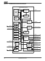
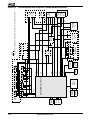
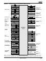
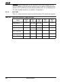
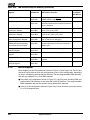
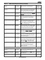
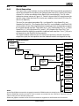
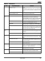
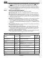
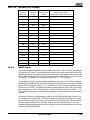
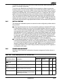
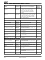
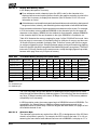
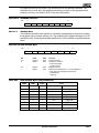
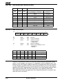
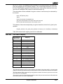
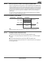
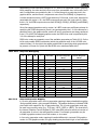
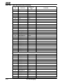
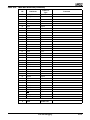
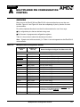
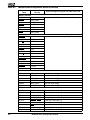
1
ÉlanSC400 and ÉlanSC410 Microcontrollers User’s Manual © 1997 Advanced Micro Devices, Inc. All rights reserved. Advanced Micro Devices, Inc. (“AMD”) reserves the right to make changes in its products without notice in order to improve design or performance characteristics. The information in this publication is believed to be accurate at the time of publication, but AMD makes no representations or warranties with respect to the accuracy or completeness of the contents of this publication or the information contained herein, and reserves the right to make changes at any time, without notice. AMD disclaims responsibility for any consequences resulting from the use of the information included in this publication. This publication neither states nor implies any representations or warranties of any kind, including but not limited to, any implied warranty of merchantability or fitness for a particular purpose. AMD products are not authorized for use as critical components in life support devices or systems without AMD’s written approval. AMD assumes no liability whatsoever for claims associated with the sale or use (including the use of engineering samples) of AMD products except as provided in AMD’s Terms and Conditions of Sale for such products. Trademarks AMD, the AMD logo and combinations thereof are trademarks of Advanced Micro Devices, Inc. Am386 and Am486 are registered trademarks, and Am186, Am188, E86, K86, Élan, Systems in Silicon, and AMD Facts-On-Demand are trademarks of Advanced Micro Devices, Inc. FusionE86 is a service mark of Advanced Micro Devices, Inc. Microsoft and Windows are registered trademarks of Microsoft Corp. Product names used in this publication are for identification purposes and may be trademarks of their respective companies. IF YOU HAVE QUESTIONS, WE’RE HERE TO HELP YOU. Customer Service The AMD customer service network includes U.S. offices, international offices, and a customer training center. Expert technical assistance is available from the worldwide staff of AMD field application engineers and factory support staff to answer E86™ family hardware and software development questions. Hotline and World Wide Web Support For answers to technical questions, AMD provides a toll-free number for direct access to our corporate applications hotline. Also available is the AMD World Wide Web home page and FTP site, which provides the latest E86 family product information, including technical information and data on upcoming product releases. For technical support questions on all E86 products, send E-mail to [email protected]. Corporate Applications Hotline Additional contact information is listed on the back of this manual. (800) 222-9323 toll-free for U.S. and Canada 44-(0) 1276-803-299 U.K. and Europe hotline World Wide Web Home Page and FTP Site To access the AMD home page go to http://www.amd.com. To download documents and software, ftp to ftp.amd.com and log on as anonymous using your E-mail address as a password. Or via your web browser, go to ftp://ftp.amd.com. Questions, requests, and input concerning AMD’s WWW pages can be sent via E-mail to [email protected]. Documentation and Literature Free E86 family information such as data books, user’s manuals, data sheets, application notes, the FusionE86SM Partner Solutions Catalog, and other literature is available with a simple phone call. Internationally, contact your local AMD sales office for complete E86 family literature. Literature Ordering (800) 222-9323 toll-free for U.S. and Canada (512) 602-5651 direct dial worldwide (512) 602-7639 fax (800) 222-9323 AMD Facts-On-DemandTM faxback service toll-free for U.S. and Canada iii iv TABLE OF CONTENTS PREFACE INTRODUCTION XXI ÉlanSC400 and ÉlanSC410 Microcontrollers. . . . . . . . . . . . . . . . . . . . . . . xxi Purpose of This Manual . . . . . . . . . . . . . . . . . . . . . . . . . . . . . . . . . . . . . . . xxi Intended Audience . . . . . . . . . . . . . . . . . . . . . . . . . . . . . . . . . . . . xxi Overview of This Manual . . . . . . . . . . . . . . . . . . . . . . . . . . . . . . . xxi Related Documents . . . . . . . . . . . . . . . . . . . . . . . . . . . . . . . . . . . . . . . . . xxiv AMD Documentation . . . . . . . . . . . . . . . . . . . . . . . . . . . . . . . . . xxiv Additional Information . . . . . . . . . . . . . . . . . . . . . . . . . . . . . . . . . xxiv Documentation Conventions . . . . . . . . . . . . . . . . . . . . . . . . . . . . . . . . . . . xxv CHAPTER 1 ARCHITECTURAL OVERVIEW 1-1 1.1 ÉlanSC400 and ÉlanSC410 Microcontrollers. . . . . . . . . . . . . . . . . . . . . . . 1-1 1.1.1 ÉlanSC400 Microcontroller . . . . . . . . . . . . . . . . . . . . . . . . . . . . . . 1-2 1.1.2 ÉlanSC410 Microcontroller . . . . . . . . . . . . . . . . . . . . . . . . . . . . . . 1-2 1.2 Architectural Overview . . . . . . . . . . . . . . . . . . . . . . . . . . . . . . . . . . . . . . . . 1-5 1.2.1 Low-Voltage Am486 CPU Core. . . . . . . . . . . . . . . . . . . . . . . . . . . 1-6 1.2.2 Power Management . . . . . . . . . . . . . . . . . . . . . . . . . . . . . . . . . . . 1-6 1.2.3 Clock Generation. . . . . . . . . . . . . . . . . . . . . . . . . . . . . . . . . . . . . . 1-6 1.2.4 ROM/Flash Interface . . . . . . . . . . . . . . . . . . . . . . . . . . . . . . . . . . . 1-7 1.2.5 DRAM Controller . . . . . . . . . . . . . . . . . . . . . . . . . . . . . . . . . . . . . . 1-7 1.2.6 Integrated Standard PC/AT Peripherals . . . . . . . . . . . . . . . . . . . . 1-8 1.2.6.1 Dual DMA Controllers . . . . . . . . . . . . . . . . . . . . . . . . . . . 1-8 1.2.6.2 Dual Interrupt Controllers . . . . . . . . . . . . . . . . . . . . . . . . 1-8 1.2.6.3 Programmable Interval Timer (PIT). . . . . . . . . . . . . . . . . 1-9 1.2.6.4 Real-Time Clock (RTC) . . . . . . . . . . . . . . . . . . . . . . . . . . 1-9 1.2.6.5 PC/AT Support Features . . . . . . . . . . . . . . . . . . . . . . . . . 1-9 1.2.7 Bidirectional Enhanced Parallel Port (EPP). . . . . . . . . . . . . . . . . . 1-9 1.2.8 Serial Port . . . . . . . . . . . . . . . . . . . . . . . . . . . . . . . . . . . . . . . . . . 1-10 1.2.9 Keyboard Interfaces . . . . . . . . . . . . . . . . . . . . . . . . . . . . . . . . . . 1-10 1.2.10 Programmable General-Purpose Inputs and Outputs . . . . . . . . . 1-11 1.2.11 Infrared Port . . . . . . . . . . . . . . . . . . . . . . . . . . . . . . . . . . . . . . . . 1-11 1.2.12 Dual PC Card Controller (ÉlanSC400 Microcontroller Only) . . . 1-11 1.2.13 Graphics Controller (ÉlanSC400 Microcontroller Only) . . . . . . . 1-12 1.2.14 JTAG Test Features . . . . . . . . . . . . . . . . . . . . . . . . . . . . . . . . . . 1-13 1.2.15 System Interfaces . . . . . . . . . . . . . . . . . . . . . . . . . . . . . . . . . . . . 1-13 1.2.15.1 Data Buses . . . . . . . . . . . . . . . . . . . . . . . . . . . . . . . . . . 1-13 1.2.15.2 Address Buses . . . . . . . . . . . . . . . . . . . . . . . . . . . . . . . 1-14 1.2.15.3 Memory Management . . . . . . . . . . . . . . . . . . . . . . . . . . 1-14 1.2.15.4 ISA Bus Interface For External ISA Peripherals . . . . . . 1-15 1.2.15.5 VESA Local (VL) Bus Interface . . . . . . . . . . . . . . . . . . . 1-15 1.3 System Considerations . . . . . . . . . . . . . . . . . . . . . . . . . . . . . . . . . . . . . . 1-16 Table of Contents v vi CHAPTER 2 CONFIGURATION BASICS 2-1 2.1 Overview . . . . . . . . . . . . . . . . . . . . . . . . . . . . . . . . . . . . . . . . . . . . . . . . . . 2-1 2.2 Configuration Methods . . . . . . . . . . . . . . . . . . . . . . . . . . . . . . . . . . . . . . . . 2-1 2.3 Configuration Register Spaces And Indexed Addressing . . . . . . . . . . . . . 2-2 2.3.1 Direct-Mapped Registers . . . . . . . . . . . . . . . . . . . . . . . . . . . . . . . 2-2 2.3.2 Indirect-Mapped Registers (Indexed Registers) . . . . . . . . . . . . . . 2-3 2.3.3 Chip Setup and Control (CSC) Indexed Registers . . . . . . . . . . . . 2-6 2.4 Feature Trade-Offs . . . . . . . . . . . . . . . . . . . . . . . . . . . . . . . . . . . . . . . . . . . 2-7 2.4.1 Pin Multiplexing . . . . . . . . . . . . . . . . . . . . . . . . . . . . . . . . . . . . . . 2-7 2.4.2 Pin Termination . . . . . . . . . . . . . . . . . . . . . . . . . . . . . . . . . . . . . . 2-7 CHAPTER 3 3-1 Am486® CPU 3.1 Overview . . . . . . . . . . . . . . . . . . . . . . . . . . . . . . . . . . . . . . . . . . . . . . . . . . 3-1 3.2 Registers . . . . . . . . . . . . . . . . . . . . . . . . . . . . . . . . . . . . . . . . . . . . . . . . . . 3-1 3.3 CPU features Specific to the ÉlanSC400 and ÉlanSC410 Microcontrollers . . . . . . . . . . . . . . . . . . . . . . . . . . . . . . . . . . . . . . . . . . . . . 3-2 3.4 Cache Memory Management . . . . . . . . . . . . . . . . . . . . . . . . . . . . . . . . . . . 3-3 3.5 System Management Mode (SMM) . . . . . . . . . . . . . . . . . . . . . . . . . . . . . . 3-3 3.5.1 Uses of SMM . . . . . . . . . . . . . . . . . . . . . . . . . . . . . . . . . . . . . . . . 3-3 3.5.2 SMM Requirements . . . . . . . . . . . . . . . . . . . . . . . . . . . . . . . . . . . 3-4 3.5.3 System Management Random Access Memory (SMRAM) . . . . . 3-4 3.5.4 System Management Interrupt (SMI) . . . . . . . . . . . . . . . . . . . . . . 3-5 3.5.4.1 State Save Map. . . . . . . . . . . . . . . . . . . . . . . . . . . . . . . . 3-6 3.5.5 SMM Execution Environment . . . . . . . . . . . . . . . . . . . . . . . . . . . . 3-8 3.5.6 Exceptions and Interrupts . . . . . . . . . . . . . . . . . . . . . . . . . . . . . . . 3-9 3.5.7 Auto Halt Restart . . . . . . . . . . . . . . . . . . . . . . . . . . . . . . . . . . . . 3-10 3.5.8 I/O Trapping . . . . . . . . . . . . . . . . . . . . . . . . . . . . . . . . . . . . . . . . 3-10 3.5.8.1 Restarting I/O Instructions. . . . . . . . . . . . . . . . . . . . . . . 3-10 3.5.8.2 Emulating I/O Instructions . . . . . . . . . . . . . . . . . . . . . . . 3-11 3.5.9 SMM Base Relocation Example . . . . . . . . . . . . . . . . . . . . . . . . . 3-11 3.5.10 SMM Interaction With SRESET . . . . . . . . . . . . . . . . . . . . . . . . . 3-17 3.6 CPU Core Identification Using the CPUID Instruction . . . . . . . . . . . . . . . 3-18 3.6.1 CPUID Timing . . . . . . . . . . . . . . . . . . . . . . . . . . . . . . . . . . . . . . . 3-18 3.6.2 CPUID Operation . . . . . . . . . . . . . . . . . . . . . . . . . . . . . . . . . . . . 3-19 3.6.3 CPUID Example . . . . . . . . . . . . . . . . . . . . . . . . . . . . . . . . . . . . . 3-20 CHAPTER 4 SYSTEM INTERFACES 4-1 4.1 Initialization. . . . . . . . . . . . . . . . . . . . . . . . . . . . . . . . . . . . . . . . . . . . . . . . . 4-1 4.1.1 Types of Reset . . . . . . . . . . . . . . . . . . . . . . . . . . . . . . . . . . . . . . . 4-1 4.1.1.1 Power-On Reset . . . . . . . . . . . . . . . . . . . . . . . . . . . . . . . 4-2 4.1.1.2 Am486 CPU DX Register at CPU Reset . . . . . . . . . . . . . 4-4 4.2 Signal Descriptions. . . . . . . . . . . . . . . . . . . . . . . . . . . . . . . . . . . . . . . . . . . 4-5 4.3 Pin Changes for the ÉlanSC410 Microcontroller . . . . . . . . . . . . . . . . . . . 4-13 4.4 Multiplexed Pin Function Options . . . . . . . . . . . . . . . . . . . . . . . . . . . . . . . 4-13 4.4.1 Using the Configuration Pins to Select Pin Functions . . . . . . . . 4-16 4.4.1.1 CFG0 and CFG1 Pins . . . . . . . . . . . . . . . . . . . . . . . . . . 4-16 4.4.1.2 CFG2 Pin . . . . . . . . . . . . . . . . . . . . . . . . . . . . . . . . . . . 4-17 4.4.1.3 CFG3 Pin . . . . . . . . . . . . . . . . . . . . . . . . . . . . . . . . . . . 4-17 4.4.1.4 BNDSCN_EN Pin . . . . . . . . . . . . . . . . . . . . . . . . . . . . . 4-17 4.5 Data and Address Buses . . . . . . . . . . . . . . . . . . . . . . . . . . . . . . . . . . . . . 4-18 4.5.1 Data Buses . . . . . . . . . . . . . . . . . . . . . . . . . . . . . . . . . . . . . . . . . 4-18 4.5.1.1 Configuration A: 16-Bit DRAM Bus and 16-Bit SD Bus. 4-19 4.5.1.2 Configuration B: 32-Bit DRAM Bus and 16-Bit SD Bus. 4-19 4.5.1.3 Configuration C: 32-Bit DRAM Bus, 16-Bit SD Bus, and 32-Bit ROM Bus . . . . . . . . . . . . . . . . . . . . . . . . . . . 4-19 4.5.1.4 Data Paths . . . . . . . . . . . . . . . . . . . . . . . . . . . . . . . . . . 4-20 Table of Contents 4.5.2 Address Buses . . . . . . . . . . . . . . . . . . . . . . . . . . . . . . . . . . . . . . 4-24 4.6 System Interfaces. . . . . . . . . . . . . . . . . . . . . . . . . . . . . . . . . . . . . . . . . . . 4-25 4.7 ISA Bus Interface . . . . . . . . . . . . . . . . . . . . . . . . . . . . . . . . . . . . . . . . . . . 4-25 4.7.1 Overview . . . . . . . . . . . . . . . . . . . . . . . . . . . . . . . . . . . . . . . . . . . 4-25 4.7.2 Registers . . . . . . . . . . . . . . . . . . . . . . . . . . . . . . . . . . . . . . . . . . 4-25 4.7.3 Block Diagram . . . . . . . . . . . . . . . . . . . . . . . . . . . . . . . . . . . . . . 4-26 4.7.4 Supported ISA Signals . . . . . . . . . . . . . . . . . . . . . . . . . . . . . . . . 4-28 4.7.5 Operation . . . . . . . . . . . . . . . . . . . . . . . . . . . . . . . . . . . . . . . . . . 4-29 4.7.5.1 Bus Speeds . . . . . . . . . . . . . . . . . . . . . . . . . . . . . . . . . . 4-29 4.7.5.2 Addressing . . . . . . . . . . . . . . . . . . . . . . . . . . . . . . . . . . 4-29 4.7.5.3 Command Strobes . . . . . . . . . . . . . . . . . . . . . . . . . . . . 4-29 4.7.5.4 External Buffer Control Signals . . . . . . . . . . . . . . . . . . . 4-30 4.7.6 Using the ISA Bus for Debugging . . . . . . . . . . . . . . . . . . . . . . . . 4-31 4.7.6.1 Echoing Direct-Mapped PC/AT Registers . . . . . . . . . . . 4-31 4.7.6.2 Echoing CSC Indexed Registers. . . . . . . . . . . . . . . . . . 4-33 4.7.7 Initialization . . . . . . . . . . . . . . . . . . . . . . . . . . . . . . . . . . . . . . . . . 4-34 4.7.8 Power Management . . . . . . . . . . . . . . . . . . . . . . . . . . . . . . . . . . 4-34 4.8 VESA Local (VL) Bus Controller. . . . . . . . . . . . . . . . . . . . . . . . . . . . . . . . 4-35 4.8.1 Overview . . . . . . . . . . . . . . . . . . . . . . . . . . . . . . . . . . . . . . . . . . . 4-35 4.8.2 Registers . . . . . . . . . . . . . . . . . . . . . . . . . . . . . . . . . . . . . . . . . . 4-35 4.8.3 Block Diagram . . . . . . . . . . . . . . . . . . . . . . . . . . . . . . . . . . . . . . 4-36 4.8.4 Operation . . . . . . . . . . . . . . . . . . . . . . . . . . . . . . . . . . . . . . . . . . 4-36 4.8.4.1 Address Interface . . . . . . . . . . . . . . . . . . . . . . . . . . . . . 4-36 4.8.4.2 Data Interface . . . . . . . . . . . . . . . . . . . . . . . . . . . . . . . . 4-36 4.8.4.3 Normal Bus Cycles . . . . . . . . . . . . . . . . . . . . . . . . . . . . 4-37 4.8.4.4 Special Bus Cycles . . . . . . . . . . . . . . . . . . . . . . . . . . . . 4-37 4.8.4.5 Unsupported VL-Bus Signal . . . . . . . . . . . . . . . . . . . . . 4-38 4.8.5 Initialization . . . . . . . . . . . . . . . . . . . . . . . . . . . . . . . . . . . . . . . . . 4-38 4.8.6 Power Management . . . . . . . . . . . . . . . . . . . . . . . . . . . . . . . . . . 4-38 4.9 PC/AT Port Logic . . . . . . . . . . . . . . . . . . . . . . . . . . . . . . . . . . . . . . . . . . . 4-39 4.9.1 Overview . . . . . . . . . . . . . . . . . . . . . . . . . . . . . . . . . . . . . . . . . . . 4-39 4.9.2 Registers . . . . . . . . . . . . . . . . . . . . . . . . . . . . . . . . . . . . . . . . . . 4-39 4.9.2.1 Direct-Mapped Registers . . . . . . . . . . . . . . . . . . . . . . . 4-39 CHAPTER 5 POWER MANAGEMENT 5-1 5.1 Overview . . . . . . . . . . . . . . . . . . . . . . . . . . . . . . . . . . . . . . . . . . . . . . . . . . 5-1 5.1.1 PMU Terms . . . . . . . . . . . . . . . . . . . . . . . . . . . . . . . . . . . . . . . . . 5-1 5.2 Registers . . . . . . . . . . . . . . . . . . . . . . . . . . . . . . . . . . . . . . . . . . . . . . . . . . 5-2 5.2.1 PMU Mode Control and Status Registers . . . . . . . . . . . . . . . . . . . 5-2 5.3 Block Diagram . . . . . . . . . . . . . . . . . . . . . . . . . . . . . . . . . . . . . . . . . . . . . . 5-8 5.4 Operation . . . . . . . . . . . . . . . . . . . . . . . . . . . . . . . . . . . . . . . . . . . . . . . . . . 5-9 5.4.1 Hyper-Speed Mode . . . . . . . . . . . . . . . . . . . . . . . . . . . . . . . . . . 5-10 5.4.1.1 Actions Taken During Hyper-Speed Mode . . . . . . . . . . 5-10 5.4.1.2 Entering Hyper-Speed Mode. . . . . . . . . . . . . . . . . . . . . 5-11 5.4.1.3 Leaving Hyper-Speed Mode . . . . . . . . . . . . . . . . . . . . . 5-11 5.4.2 High-Speed Mode . . . . . . . . . . . . . . . . . . . . . . . . . . . . . . . . . . . . 5-11 5.4.2.1 Actions Taken During High-Speed Mode . . . . . . . . . . . 5-12 5.4.2.2 Entering High-Speed Mode . . . . . . . . . . . . . . . . . . . . . . 5-12 5.4.2.3 Leaving High-Speed Mode . . . . . . . . . . . . . . . . . . . . . . 5-12 5.4.3 Low-Speed Mode . . . . . . . . . . . . . . . . . . . . . . . . . . . . . . . . . . . . 5-13 5.4.3.1 Actions Taken During Low-Speed Mode. . . . . . . . . . . . 5-13 5.4.3.2 Entering Low-Speed Mode . . . . . . . . . . . . . . . . . . . . . . 5-13 5.4.3.3 Leaving Low-Speed mode . . . . . . . . . . . . . . . . . . . . . . 5-13 5.4.4 Standby Mode . . . . . . . . . . . . . . . . . . . . . . . . . . . . . . . . . . . . . . 5-14 5.4.4.1 Actions Taken During Standby Mode . . . . . . . . . . . . . . 5-14 5.4.4.2 Entering Standby Mode. . . . . . . . . . . . . . . . . . . . . . . . . 5-14 5.4.4.3 Leaving Standby Mode . . . . . . . . . . . . . . . . . . . . . . . . . 5-14 Table of Contents vii 5.4.5 Suspend Mode . . . . . . . . . . . . . . . . . . . . . . . . . . . . . . . . . . . . . . 5-15 5.4.5.1 Actions Taken During Suspend Mode. . . . . . . . . . . . . . 5-15 5.4.5.2 Entering Suspend Mode . . . . . . . . . . . . . . . . . . . . . . . . 5-15 5.4.5.3 Leaving Suspend Mode . . . . . . . . . . . . . . . . . . . . . . . . 5-15 5.4.6 Critical Suspend Mode . . . . . . . . . . . . . . . . . . . . . . . . . . . . . . . . 5-16 5.4.6.1 Actions Taken During Critical Suspend Mode. . . . . . . . 5-16 5.4.6.2 Entering Critical Suspend Mode . . . . . . . . . . . . . . . . . . 5-16 5.4.6.3 Leaving Critical Suspend Mode . . . . . . . . . . . . . . . . . . 5-16 5.4.7 Temporary Low-Speed Mode . . . . . . . . . . . . . . . . . . . . . . . . . . . 5-17 5.4.7.1 Actions Taken During Temporary Low-Speed Mode . . 5-17 5.4.7.2 Entering Temporary Low-Speed Mode . . . . . . . . . . . . . 5-17 5.4.7.3 Leaving Temporary Low-Speed Mode . . . . . . . . . . . . . 5-18 5.4.8 PMU Flowcharts . . . . . . . . . . . . . . . . . . . . . . . . . . . . . . . . . . . . . 5-19 5.4.9 Wake-Up Sources . . . . . . . . . . . . . . . . . . . . . . . . . . . . . . . . . . . 5-21 5.4.10 General-Purpose I/O (GPIO) Pins . . . . . . . . . . . . . . . . . . . . . . . 5-24 5.4.10.1 Mappable GPIO_PMUA–GPIO_PMUD Signals . . . . . . 5-24 5.4.11 ACIN Detect and Battery Low . . . . . . . . . . . . . . . . . . . . . . . . . . . 5-24 5.4.11.1 ACIN . . . . . . . . . . . . . . . . . . . . . . . . . . . . . . . . . . . . . . . 5-25 5.4.11.2 Battery Low . . . . . . . . . . . . . . . . . . . . . . . . . . . . . . . . . . 5-25 5.4.12 SMI/NMI Generation . . . . . . . . . . . . . . . . . . . . . . . . . . . . . . . . . . 5-30 5.4.12.1 I/O Access SMIs . . . . . . . . . . . . . . . . . . . . . . . . . . . . . . 5-31 5.4.13 Activity Monitor . . . . . . . . . . . . . . . . . . . . . . . . . . . . . . . . . . . . . . 5-32 5.4.13.1 Using the Activity Source Flag Registers . . . . . . . . . . . 5-33 5.4.14 State Options in PMU Modes . . . . . . . . . . . . . . . . . . . . . . . . . . . 5-36 5.4.14.1 Suspend State Options . . . . . . . . . . . . . . . . . . . . . . . . . 5-36 5.4.14.2 Programmable Pull-Up and Pull-Down Options . . . . . . 5-36 5.5 Initialization. . . . . . . . . . . . . . . . . . . . . . . . . . . . . . . . . . . . . . . . . . . . . . . . 5-36 CHAPTER 6 viii CLOCK CONTROL 6-1 6.1 Overview . . . . . . . . . . . . . . . . . . . . . . . . . . . . . . . . . . . . . . . . . . . . . . . . . . 6-1 6.2 Registers . . . . . . . . . . . . . . . . . . . . . . . . . . . . . . . . . . . . . . . . . . . . . . . . . . 6-1 6.3 Block Diagram . . . . . . . . . . . . . . . . . . . . . . . . . . . . . . . . . . . . . . . . . . . . . . 6-1 6.4 Operation . . . . . . . . . . . . . . . . . . . . . . . . . . . . . . . . . . . . . . . . . . . . . . . . . . 6-3 6.4.1 Clock Generation . . . . . . . . . . . . . . . . . . . . . . . . . . . . . . . . . . . . . 6-3 6.4.1.1 32-KHz Crystal Oscillator . . . . . . . . . . . . . . . . . . . . . . . . 6-5 6.4.1.2 Intermediate and Low-Speed PLLs . . . . . . . . . . . . . . . . . 6-5 6.4.1.3 Graphics Dot Clock PLL . . . . . . . . . . . . . . . . . . . . . . . . . 6-6 6.4.1.4 High-Speed PLL . . . . . . . . . . . . . . . . . . . . . . . . . . . . . . . 6-7 6.4.2 Clock Control . . . . . . . . . . . . . . . . . . . . . . . . . . . . . . . . . . . . . . . . 6-8 6.4.2.1 CPU 1x Clock . . . . . . . . . . . . . . . . . . . . . . . . . . . . . . . . . 6-8 6.4.2.2 Memory Clock . . . . . . . . . . . . . . . . . . . . . . . . . . . . . . . . . 6-8 6.4.2.3 Timer Clock . . . . . . . . . . . . . . . . . . . . . . . . . . . . . . . . . . . 6-8 6.4.2.4 UART Clock . . . . . . . . . . . . . . . . . . . . . . . . . . . . . . . . . . 6-8 6.4.2.5 System Clock . . . . . . . . . . . . . . . . . . . . . . . . . . . . . . . . . 6-8 6.4.2.6 RTC Clock . . . . . . . . . . . . . . . . . . . . . . . . . . . . . . . . . . . . 6-8 6.4.2.7 DMA Clock . . . . . . . . . . . . . . . . . . . . . . . . . . . . . . . . . . . 6-8 6.5 Initialization. . . . . . . . . . . . . . . . . . . . . . . . . . . . . . . . . . . . . . . . . . . . . . . . 6-11 6.6 Power Management . . . . . . . . . . . . . . . . . . . . . . . . . . . . . . . . . . . . . . . . . 6-11 Table of Contents CHAPTER 7 MEMORY MANAGEMENT 7-1 7.1 Overview . . . . . . . . . . . . . . . . . . . . . . . . . . . . . . . . . . . . . . . . . . . . . . . . . . 7-1 7.2 Registers . . . . . . . . . . . . . . . . . . . . . . . . . . . . . . . . . . . . . . . . . . . . . . . . . . 7-1 7.3 Address Decoding and Aliasing . . . . . . . . . . . . . . . . . . . . . . . . . . . . . . . . . 7-3 7.3.1 Internal Address Bus Size . . . . . . . . . . . . . . . . . . . . . . . . . . . . . . 7-3 7.3.2 Special Handling for A20 . . . . . . . . . . . . . . . . . . . . . . . . . . . . . . . 7-3 7.3.3 Top of Memory CPU Execution . . . . . . . . . . . . . . . . . . . . . . . . . . 7-3 7.3.4 ISA Bus Addressing . . . . . . . . . . . . . . . . . . . . . . . . . . . . . . . . . . . 7-4 7.4 Multiple Memory Spaces . . . . . . . . . . . . . . . . . . . . . . . . . . . . . . . . . . . . . . 7-4 7.5 Non-Translated Memory Management. . . . . . . . . . . . . . . . . . . . . . . . . . . . 7-6 7.5.1 ROM0 and Non-Translated Memory Management . . . . . . . . . . . 7-6 7.5.2 DRAM and Non-Translated Memory Management . . . . . . . . . . . 7-7 7.6 Translated Memory Management . . . . . . . . . . . . . . . . . . . . . . . . . . . . . . . 7-8 7.6.1 MMS Windows A and B . . . . . . . . . . . . . . . . . . . . . . . . . . . . . . . . 7-8 7.6.2 MMS Windows C, D, E, and F . . . . . . . . . . . . . . . . . . . . . . . . . . . 7-9 7.6.3 Graphics Frame Buffer MMS Window . . . . . . . . . . . . . . . . . . . . . 7-9 7.6.4 PC Card Memory Management . . . . . . . . . . . . . . . . . . . . . . . . . 7-10 7.6.4.1 Standard 82365 PC Card Control . . . . . . . . . . . . . . . . . 7-10 7.6.4.2 Simplified PC Card Control . . . . . . . . . . . . . . . . . . . . . . 7-10 7.7 System Considerations . . . . . . . . . . . . . . . . . . . . . . . . . . . . . . . . . . . . . . 7-11 7.7.1 2.7-Volt Operation . . . . . . . . . . . . . . . . . . . . . . . . . . . . . . . . . . . 7-11 7.7.2 ROMCS2 Operation . . . . . . . . . . . . . . . . . . . . . . . . . . . . . . . . . . 7-11 7.7.3 Memory Mapping and Caching . . . . . . . . . . . . . . . . . . . . . . . . . . 7-11 7.7.3.1 Caching in System Management Mode . . . . . . . . . . . . 7-12 CHAPTER 8 ROM/FLASH INTERFACE 8-1 8.1 Overview . . . . . . . . . . . . . . . . . . . . . . . . . . . . . . . . . . . . . . . . . . . . . . . . . . 8-1 8.2 Registers . . . . . . . . . . . . . . . . . . . . . . . . . . . . . . . . . . . . . . . . . . . . . . . . . . 8-1 8.3 Block Diagram . . . . . . . . . . . . . . . . . . . . . . . . . . . . . . . . . . . . . . . . . . . . . . 8-2 8.4 Operation . . . . . . . . . . . . . . . . . . . . . . . . . . . . . . . . . . . . . . . . . . . . . . . . . . 8-3 8.4.1 Architectural Overview . . . . . . . . . . . . . . . . . . . . . . . . . . . . . . . . . 8-3 8.4.2 Data Bus Usage . . . . . . . . . . . . . . . . . . . . . . . . . . . . . . . . . . . . . . 8-4 8.5 Initialization. . . . . . . . . . . . . . . . . . . . . . . . . . . . . . . . . . . . . . . . . . . . . . . . . 8-6 8.5.1 Configuring the ROMCS0 Interface Using Pin Straps . . . . . . . . . 8-7 8.5.2 Other ROMCSx Interface Configuration Options . . . . . . . . . . . . . 8-8 8.5.2.1 Data Width Control . . . . . . . . . . . . . . . . . . . . . . . . . . . . . 8-8 8.5.2.2 Access Speed . . . . . . . . . . . . . . . . . . . . . . . . . . . . . . . . . 8-9 8.5.2.3 Early Chip Select. . . . . . . . . . . . . . . . . . . . . . . . . . . . . . 8-10 8.6 Power Management . . . . . . . . . . . . . . . . . . . . . . . . . . . . . . . . . . . . . . . . . 8-11 CHAPTER 9 DRAM CONTROLLER 9-1 9.1 System Design . . . . . . . . . . . . . . . . . . . . . . . . . . . . . . . . . . . . . . . . . . . . . . 9-1 9.2 Registers . . . . . . . . . . . . . . . . . . . . . . . . . . . . . . . . . . . . . . . . . . . . . . . . . . 9-3 9.3 Block Diagram . . . . . . . . . . . . . . . . . . . . . . . . . . . . . . . . . . . . . . . . . . . . . . 9-4 9.4 Operation . . . . . . . . . . . . . . . . . . . . . . . . . . . . . . . . . . . . . . . . . . . . . . . . . . 9-5 9.4.1 System Address Decoding . . . . . . . . . . . . . . . . . . . . . . . . . . . . . . 9-5 9.4.1.1 RAS Strobe Assertion (Bank Selection) . . . . . . . . . . . . . 9-5 9.4.1.2 CAS Strobe Assertion (Byte Lane Selection) . . . . . . . . . 9-5 9.4.2 Timing and Control Signal Generation . . . . . . . . . . . . . . . . . . . . 9-12 9.4.2.1 Page Mode and RAS Time-Outs. . . . . . . . . . . . . . . . . . 9-12 9.4.2.2 MWE Generation. . . . . . . . . . . . . . . . . . . . . . . . . . . . . . 9-12 9.4.2.3 CAS Pulse Width. . . . . . . . . . . . . . . . . . . . . . . . . . . . . . 9-12 9.4.2.4 CAS Precharge Delay . . . . . . . . . . . . . . . . . . . . . . . . . . 9-12 9.4.2.5 Refresh . . . . . . . . . . . . . . . . . . . . . . . . . . . . . . . . . . . . . 9-12 9.5 Initialization. . . . . . . . . . . . . . . . . . . . . . . . . . . . . . . . . . . . . . . . . . . . . . . . 9-13 9.5.1 Boot Process Overview . . . . . . . . . . . . . . . . . . . . . . . . . . . . . . . 9-13 9.5.2 Dynamic DRAM Detection Algorithm . . . . . . . . . . . . . . . . . . . . . 9-14 9.6 Power Management . . . . . . . . . . . . . . . . . . . . . . . . . . . . . . . . . . . . . . . . . 9-15 Table of Contents ix CHAPTER 10 DMA CONTROLLER 10-1 10.1 Overview . . . . . . . . . . . . . . . . . . . . . . . . . . . . . . . . . . . . . . . . . . . . . . . . . 10-1 10.2 Registers . . . . . . . . . . . . . . . . . . . . . . . . . . . . . . . . . . . . . . . . . . . . . . . . . 10-1 10.2.1 Direct-Mapped Registers . . . . . . . . . . . . . . . . . . . . . . . . . . . . . . 10-1 10.2.2 Chip Configuration and Control (CSC) Registers . . . . . . . . . . . . 10-2 10.2.2.1 Extended Page Registers . . . . . . . . . . . . . . . . . . . . . . . 10-2 10.3 Block Diagram . . . . . . . . . . . . . . . . . . . . . . . . . . . . . . . . . . . . . . . . . . . . . 10-3 10.4 Operation . . . . . . . . . . . . . . . . . . . . . . . . . . . . . . . . . . . . . . . . . . . . . . . . . 10-5 10.4.1 Addressing DMA Channels . . . . . . . . . . . . . . . . . . . . . . . . . . . . 10-5 10.4.2 DMA Transfers . . . . . . . . . . . . . . . . . . . . . . . . . . . . . . . . . . . . . . 10-6 10.4.2.1 Transfer Modes . . . . . . . . . . . . . . . . . . . . . . . . . . . . . . . 10-7 10.4.2.2 Autoinitialize . . . . . . . . . . . . . . . . . . . . . . . . . . . . . . . . . 10-7 10.4.2.3 Priority . . . . . . . . . . . . . . . . . . . . . . . . . . . . . . . . . . . . . . 10-7 10.4.2.4 DMA Cycles . . . . . . . . . . . . . . . . . . . . . . . . . . . . . . . . . 10-7 10.4.3 DMA Channel Mapping . . . . . . . . . . . . . . . . . . . . . . . . . . . . . . . 10-8 10.4.4 DMA Latency . . . . . . . . . . . . . . . . . . . . . . . . . . . . . . . . . . . . . . . 10-9 10.5 Initialization. . . . . . . . . . . . . . . . . . . . . . . . . . . . . . . . . . . . . . . . . . . . . . . . 10-9 10.6 Power Management . . . . . . . . . . . . . . . . . . . . . . . . . . . . . . . . . . . . . . . . . 10-9 CHAPTER 11 PROGRAMMABLE INTERRUPT CONTROLLER 11-1 11.1 Overview . . . . . . . . . . . . . . . . . . . . . . . . . . . . . . . . . . . . . . . . . . . . . . . . . 11-1 11.2 Registers . . . . . . . . . . . . . . . . . . . . . . . . . . . . . . . . . . . . . . . . . . . . . . . . . 11-1 11.3 Block Diagram . . . . . . . . . . . . . . . . . . . . . . . . . . . . . . . . . . . . . . . . . . . . . 11-2 11.4 Operation . . . . . . . . . . . . . . . . . . . . . . . . . . . . . . . . . . . . . . . . . . . . . . . . . 11-3 11.4.1 IRQ Mapping . . . . . . . . . . . . . . . . . . . . . . . . . . . . . . . . . . . . . . . . 11-4 11.4.2 Interrupt Vectors . . . . . . . . . . . . . . . . . . . . . . . . . . . . . . . . . . . . . 11-5 11.5 Initialization. . . . . . . . . . . . . . . . . . . . . . . . . . . . . . . . . . . . . . . . . . . . . . . . 11-5 11.6 Power Management . . . . . . . . . . . . . . . . . . . . . . . . . . . . . . . . . . . . . . . . . 11-6 CHAPTER 12 PROGRAMMABLE INTERVAL TIMER 12-1 12.1 Overview . . . . . . . . . . . . . . . . . . . . . . . . . . . . . . . . . . . . . . . . . . . . . . . . . 12-1 12.2 Registers . . . . . . . . . . . . . . . . . . . . . . . . . . . . . . . . . . . . . . . . . . . . . . . . . 12-1 12.2.1 Direct-Mapped Registers . . . . . . . . . . . . . . . . . . . . . . . . . . . . . . 12-1 12.3 Block Diagram . . . . . . . . . . . . . . . . . . . . . . . . . . . . . . . . . . . . . . . . . . . . . 12-2 12.4 Operation . . . . . . . . . . . . . . . . . . . . . . . . . . . . . . . . . . . . . . . . . . . . . . . . . 12-3 12.4.1 Modes of Operation . . . . . . . . . . . . . . . . . . . . . . . . . . . . . . . . . . 12-3 12.4.1.1 Mode 0: Interrupt on Terminal Count . . . . . . . . . . . . . . 12-3 12.4.1.2 Mode 1: Hardware-Retriggerable One-Shot . . . . . . . . . 12-3 12.4.1.3 Mode 2: Rate Generator . . . . . . . . . . . . . . . . . . . . . . . . 12-4 12.4.1.4 Mode 3: Square Wave Mode . . . . . . . . . . . . . . . . . . . . 12-4 12.4.1.5 Mode 4: Software Triggered Strobe . . . . . . . . . . . . . . . 12-4 12.4.1.6 Mode 5: Hardware Triggered Strobe. . . . . . . . . . . . . . . 12-5 12.4.2 Timer Configuration . . . . . . . . . . . . . . . . . . . . . . . . . . . . . . . . . . 12-5 12.4.2.1 Configuring Timer Channel 0 . . . . . . . . . . . . . . . . . . . . 12-5 12.4.2.2 Configuring Timer Channel 1 . . . . . . . . . . . . . . . . . . . . 12-5 12.4.2.3 Configuring Timer Channel 2 . . . . . . . . . . . . . . . . . . . . 12-6 12.4.3 Programming the Timer Channels . . . . . . . . . . . . . . . . . . . . . . . 12-6 12.5 Initialization. . . . . . . . . . . . . . . . . . . . . . . . . . . . . . . . . . . . . . . . . . . . . . . . 12-6 12.6 Power Management . . . . . . . . . . . . . . . . . . . . . . . . . . . . . . . . . . . . . . . . . 12-6 x Table of Contents CHAPTER 13 REAL-TIME CLOCK 13-1 13.1 Overview . . . . . . . . . . . . . . . . . . . . . . . . . . . . . . . . . . . . . . . . . . . . . . . . . 13-1 13.2 Registers . . . . . . . . . . . . . . . . . . . . . . . . . . . . . . . . . . . . . . . . . . . . . . . . . 13-1 13.2.1 RTC and Configuration RAM Index Registers . . . . . . . . . . . . . . 13-2 13.3 Block Diagram . . . . . . . . . . . . . . . . . . . . . . . . . . . . . . . . . . . . . . . . . . . . . 13-3 13.3.1 Voltage Monitoring . . . . . . . . . . . . . . . . . . . . . . . . . . . . . . . . . . . 13-3 13.4 Operation . . . . . . . . . . . . . . . . . . . . . . . . . . . . . . . . . . . . . . . . . . . . . . . . . 13-5 13.4.1 Interrupts . . . . . . . . . . . . . . . . . . . . . . . . . . . . . . . . . . . . . . . . . . 13-5 13.4.2 RTC Clock . . . . . . . . . . . . . . . . . . . . . . . . . . . . . . . . . . . . . . . . . 13-6 13.4.3 Internal Oscillator Control Bits . . . . . . . . . . . . . . . . . . . . . . . . . . 13-6 13.4.4 Update Cycle . . . . . . . . . . . . . . . . . . . . . . . . . . . . . . . . . . . . . . . 13-6 13.4.5 Backup Battery Considerations . . . . . . . . . . . . . . . . . . . . . . . . . 13-6 13.4.5.1 Using an External RTC Backup Battery . . . . . . . . . . . . 13-7 13.4.5.2 Not Using an External RTC Backup Battery . . . . . . . . . 13-8 13.4.5.3 Overall System Implications . . . . . . . . . . . . . . . . . . . . . 13-8 13.5 Initialization. . . . . . . . . . . . . . . . . . . . . . . . . . . . . . . . . . . . . . . . . . . . . . . . 13-9 13.6 Power Management . . . . . . . . . . . . . . . . . . . . . . . . . . . . . . . . . . . . . . . . . 13-9 CHAPTER 14 PARALLEL PORT 14-1 14.1 Overview . . . . . . . . . . . . . . . . . . . . . . . . . . . . . . . . . . . . . . . . . . . . . . . . . 14-1 14.2 Registers . . . . . . . . . . . . . . . . . . . . . . . . . . . . . . . . . . . . . . . . . . . . . . . . . 14-1 14.2.1 Direct-Mapped Registers . . . . . . . . . . . . . . . . . . . . . . . . . . . . . . 14-1 14.2.2 Chip Setup and Control Registers . . . . . . . . . . . . . . . . . . . . . . . 14-2 14.3 Block Diagram . . . . . . . . . . . . . . . . . . . . . . . . . . . . . . . . . . . . . . . . . . . . . 14-3 14.4 Pin Definitions by Mode . . . . . . . . . . . . . . . . . . . . . . . . . . . . . . . . . . . . . . 14-4 14.5 Operation . . . . . . . . . . . . . . . . . . . . . . . . . . . . . . . . . . . . . . . . . . . . . . . . . 14-5 14.5.1 Minimal System Design . . . . . . . . . . . . . . . . . . . . . . . . . . . . . . . 14-5 14.5.1.1 PC/AT Compatible Mode . . . . . . . . . . . . . . . . . . . . . . . 14-5 14.5.1.2 Bidirectional and EPP Modes . . . . . . . . . . . . . . . . . . . . 14-5 14.5.2 Operating Modes . . . . . . . . . . . . . . . . . . . . . . . . . . . . . . . . . . . . 14-7 14.5.2.1 PC/AT Compatible Mode . . . . . . . . . . . . . . . . . . . . . . . 14-7 14.5.2.2 Bidirectional Mode. . . . . . . . . . . . . . . . . . . . . . . . . . . . . 14-7 14.5.2.3 Enhanced Parallel Port (EPP) Mode . . . . . . . . . . . . . . . 14-7 14.6 Initialization. . . . . . . . . . . . . . . . . . . . . . . . . . . . . . . . . . . . . . . . . . . . . . . 14-10 14.7 Power Management . . . . . . . . . . . . . . . . . . . . . . . . . . . . . . . . . . . . . . . . 14-10 CHAPTER 15 SERIAL PORT (UART) 15-1 15.1 Overview . . . . . . . . . . . . . . . . . . . . . . . . . . . . . . . . . . . . . . . . . . . . . . . . . 15-1 15.2 Registers . . . . . . . . . . . . . . . . . . . . . . . . . . . . . . . . . . . . . . . . . . . . . . . . . 15-1 15.2.1 Direct-Mapped Registers . . . . . . . . . . . . . . . . . . . . . . . . . . . . . . 15-1 15.2.2 Chip Setup and Control (CSC) Index Registers . . . . . . . . . . . . . 15-2 15.3 Block Diagram . . . . . . . . . . . . . . . . . . . . . . . . . . . . . . . . . . . . . . . . . . . . . 15-3 15.4 Operation . . . . . . . . . . . . . . . . . . . . . . . . . . . . . . . . . . . . . . . . . . . . . . . . . 15-4 15.4.1 Baud-Rate Generation . . . . . . . . . . . . . . . . . . . . . . . . . . . . . . . . 15-4 15.4.2 UART Frame . . . . . . . . . . . . . . . . . . . . . . . . . . . . . . . . . . . . . . . 15-5 15.4.3 Operating Modes . . . . . . . . . . . . . . . . . . . . . . . . . . . . . . . . . . . . 15-6 15.4.3.1 16450-Compatible Mode (No FIFOs) . . . . . . . . . . . . . . 15-6 15.4.3.2 16550-Compatible Mode (FIFOs) . . . . . . . . . . . . . . . . . 15-6 15.4.4 Interrupts . . . . . . . . . . . . . . . . . . . . . . . . . . . . . . . . . . . . . . . . . . 15-6 15.5 Initialization. . . . . . . . . . . . . . . . . . . . . . . . . . . . . . . . . . . . . . . . . . . . . . . . 15-7 15.6 Power Management . . . . . . . . . . . . . . . . . . . . . . . . . . . . . . . . . . . . . . . . . 15-7 Table of Contents xi CHAPTER 16 KEYBOARD INTERFACES 16-1 16.1 Overview . . . . . . . . . . . . . . . . . . . . . . . . . . . . . . . . . . . . . . . . . . . . . . . . . 16-1 16.1.1 Matrix Keyboard Interface . . . . . . . . . . . . . . . . . . . . . . . . . . . . . 16-1 16.1.2 SCP Emulation . . . . . . . . . . . . . . . . . . . . . . . . . . . . . . . . . . . . . . 16-2 16.1.3 XT Keyboard Interface . . . . . . . . . . . . . . . . . . . . . . . . . . . . . . . . 16-2 16.2 Registers . . . . . . . . . . . . . . . . . . . . . . . . . . . . . . . . . . . . . . . . . . . . . . . . . 16-3 16.3 Operation . . . . . . . . . . . . . . . . . . . . . . . . . . . . . . . . . . . . . . . . . . . . . . . . . 16-5 16.3.1 Matrix Keyboard Interface . . . . . . . . . . . . . . . . . . . . . . . . . . . . . 16-5 16.3.1.1 N-Key Rollover . . . . . . . . . . . . . . . . . . . . . . . . . . . . . . . 16-7 16.3.1.2 Key-Pressed Interrupt . . . . . . . . . . . . . . . . . . . . . . . . . . 16-7 16.3.1.3 Keyboard Wake-Up . . . . . . . . . . . . . . . . . . . . . . . . . . . . 16-8 16.3.1.4 CPU-Scanned Keyboard . . . . . . . . . . . . . . . . . . . . . . . . 16-8 16.3.1.5 Keyboard Timer. . . . . . . . . . . . . . . . . . . . . . . . . . . . . . . 16-8 16.3.1.6 Typematic Support . . . . . . . . . . . . . . . . . . . . . . . . . . . . 16-9 16.3.2 SCP Emulation . . . . . . . . . . . . . . . . . . . . . . . . . . . . . . . . . . . . . . 16-9 16.3.2.1 SCP GATEA20 and Reset CPU Command Emulation . 16-9 16.3.3 Keyboard System Scenarios . . . . . . . . . . . . . . . . . . . . . . . . . . 16-10 16.3.3.1 Simple Matrix Keyboard Support by Interrupting . . . . 16-10 16.3.3.2 Simple Matrix Keyboard Support by Polling . . . . . . . . 16-10 16.3.3.3 Matrix Keyboard Support with PC/AT Compatibility . . 16-11 16.3.4 XT Keyboard . . . . . . . . . . . . . . . . . . . . . . . . . . . . . . . . . . . . . . . 16-12 16.3.4.1 Interrupts . . . . . . . . . . . . . . . . . . . . . . . . . . . . . . . . . . . 16-12 16.3.4.2 Enabling the XT Keyboard Interface . . . . . . . . . . . . . . 16-13 16.3.4.3 Controlling the XT Keyboard Interface . . . . . . . . . . . . 16-13 16.3.4.4 Timing . . . . . . . . . . . . . . . . . . . . . . . . . . . . . . . . . . . . . 16-13 16.4 Initialization. . . . . . . . . . . . . . . . . . . . . . . . . . . . . . . . . . . . . . . . . . . . . . . 16-13 16.5 Power Management . . . . . . . . . . . . . . . . . . . . . . . . . . . . . . . . . . . . . . . . 16-13 CHAPTER 17 GENERAL-PURPOSE INPUT/OUTPUT AND PROGRAMMABLE CHIP SELECTS 17-1 17.1 Overview . . . . . . . . . . . . . . . . . . . . . . . . . . . . . . . . . . . . . . . . . . . . . . . . . 17-1 17.1.1 External Pins . . . . . . . . . . . . . . . . . . . . . . . . . . . . . . . . . . . . . . . 17-1 17.1.2 Internal Chip-Select Logic . . . . . . . . . . . . . . . . . . . . . . . . . . . . . 17-1 17.2 Registers . . . . . . . . . . . . . . . . . . . . . . . . . . . . . . . . . . . . . . . . . . . . . . . . . 17-2 17.3 Block Diagram . . . . . . . . . . . . . . . . . . . . . . . . . . . . . . . . . . . . . . . . . . . . . 17-4 17.4 GPIO System Implications . . . . . . . . . . . . . . . . . . . . . . . . . . . . . . . . . . . . 17-6 17.5 Initialization. . . . . . . . . . . . . . . . . . . . . . . . . . . . . . . . . . . . . . . . . . . . . . . . 17-6 17.5.1 GPIO Pins and Simple Input . . . . . . . . . . . . . . . . . . . . . . . . . . . . 17-6 17.5.2 GPIO Pins and Simple Output . . . . . . . . . . . . . . . . . . . . . . . . . . 17-7 17.5.3 GPIO_CS Pins and Automatic Output . . . . . . . . . . . . . . . . . . . . 17-7 17.5.3.1 Automatic PMU Information Output . . . . . . . . . . . . . . . 17-7 17.5.3.2 Automatic Chip Select Outputs . . . . . . . . . . . . . . . . . . . 17-7 17.6 GPIO_CS Signals as PMU Activities and SMI/NMI Generation . . . . . . . . 17-8 17.6.1 GPIO_CS PMU Activity and Wake-Up . . . . . . . . . . . . . . . . . . . . 17-8 17.6.2 GPIO_CS Signals and SMI/NMI Generation . . . . . . . . . . . . . . . 17-8 17.7 General-Purpose Chip Selects (GP_CSA–GP_CSD) . . . . . . . . . . . . . . . 17-8 17.7.1 Using DMA with General-Purpose Chip Selects . . . . . . . . . . . . 17-9 17.7.2 Mapping a General-Purpose Chip Select to a GPIO_CS Pin . . . 17-9 17.7.3 Using General-Purpose Chip Selects as PMU Activities . . . . . . 17-9 17.7.4 Using General-Purpose Chip Selects to Force an SMI . . . . . . . 17-9 17.8 Power Management . . . . . . . . . . . . . . . . . . . . . . . . . . . . . . . . . . . . . . . . . 17-9 xii Table of Contents CHAPTER 18 INFRARED PORT 18-1 18.1 Overview . . . . . . . . . . . . . . . . . . . . . . . . . . . . . . . . . . . . . . . . . . . . . . . . . 18-1 18.2 Registers . . . . . . . . . . . . . . . . . . . . . . . . . . . . . . . . . . . . . . . . . . . . . . . . . 18-2 18.3 Block Diagram . . . . . . . . . . . . . . . . . . . . . . . . . . . . . . . . . . . . . . . . . . . . . 18-3 18.4 Operation . . . . . . . . . . . . . . . . . . . . . . . . . . . . . . . . . . . . . . . . . . . . . . . . . 18-3 18.4.1 Slow-Speed Infrared Mode . . . . . . . . . . . . . . . . . . . . . . . . . . . . . 18-4 18.4.1.1 Hardware Support . . . . . . . . . . . . . . . . . . . . . . . . . . . . . 18-4 18.4.2 High-Speed Infrared Mode . . . . . . . . . . . . . . . . . . . . . . . . . . . . . 18-5 18.4.2.1 High-Speed IrDA Frame . . . . . . . . . . . . . . . . . . . . . . . . 18-6 18.4.2.2 Frame Sequences . . . . . . . . . . . . . . . . . . . . . . . . . . . . . 18-7 18.4.2.3 High-Speed Infrared Mode . . . . . . . . . . . . . . . . . . . . . . 18-7 18.4.2.4 Data Stream . . . . . . . . . . . . . . . . . . . . . . . . . . . . . . . . . 18-7 18.4.2.5 FIFO Usage. . . . . . . . . . . . . . . . . . . . . . . . . . . . . . . . . . 18-8 18.4.2.6 Receive and Transmit State Machines . . . . . . . . . . . . . 18-8 18.4.2.7 Frame Abort . . . . . . . . . . . . . . . . . . . . . . . . . . . . . . . . . 18-9 18.4.2.8 Sending Back-to-Back Frames . . . . . . . . . . . . . . . . . . . 18-9 18.4.2.9 Receiving Back-to-Back Frames . . . . . . . . . . . . . . . . . . 18-9 18.4.2.10Transmit Data Transfers. . . . . . . . . . . . . . . . . . . . . . . 18-10 18.4.2.11Receive Data Transfers . . . . . . . . . . . . . . . . . . . . . . . 18-11 18.4.2.12Interrupts . . . . . . . . . . . . . . . . . . . . . . . . . . . . . . . . . . 18-12 18.4.2.13Serial Infrared Interaction Pulse (SIP) Generation . . . 18-12 18.5 Initialization. . . . . . . . . . . . . . . . . . . . . . . . . . . . . . . . . . . . . . . . . . . . . . . 18-13 18.6 Power Management . . . . . . . . . . . . . . . . . . . . . . . . . . . . . . . . . . . . . . . . 18-13 CHAPTER 19 PC CARD CONTROLLER (ÉlanSC400 MICROCONTROLLER ONLY) 19-1 19.1 Overview . . . . . . . . . . . . . . . . . . . . . . . . . . . . . . . . . . . . . . . . . . . . . . . . . 19-1 19.2 Registers . . . . . . . . . . . . . . . . . . . . . . . . . . . . . . . . . . . . . . . . . . . . . . . . . 19-2 19.3 Block Diagram . . . . . . . . . . . . . . . . . . . . . . . . . . . . . . . . . . . . . . . . . . . . . 19-5 19.4 Pin Definitions by Mode . . . . . . . . . . . . . . . . . . . . . . . . . . . . . . . . . . . . . . 19-6 19.5 Operation . . . . . . . . . . . . . . . . . . . . . . . . . . . . . . . . . . . . . . . . . . . . . . . . . 19-6 19.5.1 Signal Multiplexing . . . . . . . . . . . . . . . . . . . . . . . . . . . . . . . . . . . 19-7 19.5.2 Memory Interface . . . . . . . . . . . . . . . . . . . . . . . . . . . . . . . . . . . . 19-8 19.5.2.1 Standard Mode . . . . . . . . . . . . . . . . . . . . . . . . . . . . . . . 19-8 19.5.2.2 Enhanced Mode . . . . . . . . . . . . . . . . . . . . . . . . . . . . . . 19-8 19.5.2.3 PC Card Controller Memory Windows . . . . . . . . . . . . . 19-8 19.5.3 I/O Interface . . . . . . . . . . . . . . . . . . . . . . . . . . . . . . . . . . . . . . . 19-10 19.5.3.1 I/O Windows . . . . . . . . . . . . . . . . . . . . . . . . . . . . . . . . 19-10 19.5.4 PC Card Bus Cycles . . . . . . . . . . . . . . . . . . . . . . . . . . . . . . . . . 19-11 19.5.4.1 Memory Write Protection. . . . . . . . . . . . . . . . . . . . . . . 19-13 19.5.4.2 Non-DMA Cycle Timing. . . . . . . . . . . . . . . . . . . . . . . . 19-13 19.5.5 Using Standard PC Card Mode . . . . . . . . . . . . . . . . . . . . . . . . 19-15 19.5.5.1 Memory Window Redirection . . . . . . . . . . . . . . . . . . . 19-15 19.5.5.2 Configuring MMS Windows C–F . . . . . . . . . . . . . . . . . 19-16 19.5.6 Using Enhanced PC Card Mode . . . . . . . . . . . . . . . . . . . . . . . 19-16 19.5.7 DMA Interface . . . . . . . . . . . . . . . . . . . . . . . . . . . . . . . . . . . . . . 19-17 19.5.7.1 DMA Cycle Timing . . . . . . . . . . . . . . . . . . . . . . . . . . . 19-17 19.5.8 System Interrupt Control . . . . . . . . . . . . . . . . . . . . . . . . . . . . . . 19-18 19.5.8.1 Socket Status Inputs . . . . . . . . . . . . . . . . . . . . . . . . . . 19-18 19.5.9 Sound Generation . . . . . . . . . . . . . . . . . . . . . . . . . . . . . . . . . . 19-18 19.5.10 Using the WAIT_AB, CD_A, and CD_B Pins . . . . . . . . . . . . . . 19-19 19.5.10.1WAIT_AB Signal Merging. . . . . . . . . . . . . . . . . . . . . . 19-19 19.5.10.2CD_A and CD_B Signal Merging . . . . . . . . . . . . . . . . 19-19 19.5.11 Power Considerations . . . . . . . . . . . . . . . . . . . . . . . . . . . . . . . 19-20 19.5.11.1Card VCC and VPP Control . . . . . . . . . . . . . . . . . . . . . 19-20 19.5.11.2Power Considerations for System Design . . . . . . . . . 19-21 19.6 Initialization. . . . . . . . . . . . . . . . . . . . . . . . . . . . . . . . . . . . . . . . . . . . . . . 19-22 19.6.1 Identification and Revision Register . . . . . . . . . . . . . . . . . . . . . 19-23 19.7 Power Management . . . . . . . . . . . . . . . . . . . . . . . . . . . . . . . . . . . . . . . . 19-24 Table of Contents xiii CHAPTER 20 GRAPHICS CONTROLLER (ÉlanSC400 MICROCONTROLLER ONLY) 20-1 20.1 Overview . . . . . . . . . . . . . . . . . . . . . . . . . . . . . . . . . . . . . . . . . . . . . . . . . 20-1 20.2 Registers . . . . . . . . . . . . . . . . . . . . . . . . . . . . . . . . . . . . . . . . . . . . . . . . . 20-2 20.3 Block Diagram . . . . . . . . . . . . . . . . . . . . . . . . . . . . . . . . . . . . . . . . . . . . . 20-6 20.4 Operation . . . . . . . . . . . . . . . . . . . . . . . . . . . . . . . . . . . . . . . . . . . . . . . . . 20-6 20.4.1 Using the Graphics Controller . . . . . . . . . . . . . . . . . . . . . . . . . . 20-6 20.4.1.1 Interrupts and I/O Trapping . . . . . . . . . . . . . . . . . . . . . . 20-6 20.4.1.2 Clock Control. . . . . . . . . . . . . . . . . . . . . . . . . . . . . . . . . 20-7 20.4.1.3 Screen Timing Generation and Cursor Control . . . . . . . 20-7 20.4.1.4 Internal Unified Memory Architecture . . . . . . . . . . . . . . 20-8 20.4.2 Graphics Buffers . . . . . . . . . . . . . . . . . . . . . . . . . . . . . . . . . . . . . 20-8 20.4.2.1 Using the Frame Buffer in Text Mode . . . . . . . . . . . . . . 20-8 20.4.2.2 Using the Frame Buffer in Graphics Mode . . . . . . . . . . 20-9 20.4.2.3 Graphics Mode Memory Maps . . . . . . . . . . . . . . . . . . . 20-9 20.4.2.4 Font Buffer . . . . . . . . . . . . . . . . . . . . . . . . . . . . . . . . . 20-10 20.4.2.5 Managing Graphics Memory . . . . . . . . . . . . . . . . . . . . 20-10 20.4.3 CGA Graphics Modes . . . . . . . . . . . . . . . . . . . . . . . . . . . . . . . . 20-11 20.4.3.1 CGA Graphics Pixel Formats . . . . . . . . . . . . . . . . . . . 20-12 20.4.3.2 CGA Graphics Color Processing. . . . . . . . . . . . . . . . . 20-13 20.4.4 HGA Graphics Modes . . . . . . . . . . . . . . . . . . . . . . . . . . . . . . . . 20-13 20.4.4.1 HGA Graphics Mode Memory Model . . . . . . . . . . . . . 20-14 20.4.4.2 HGA Graphics Pixel Formats . . . . . . . . . . . . . . . . . . . 20-15 20.4.5 CGA/MDA Text Modes . . . . . . . . . . . . . . . . . . . . . . . . . . . . . . . 20-15 20.4.5.1 Data Structures . . . . . . . . . . . . . . . . . . . . . . . . . . . . . . 20-15 20.4.5.2 Cursor Generation. . . . . . . . . . . . . . . . . . . . . . . . . . . . 20-20 20.4.5.3 Fonts . . . . . . . . . . . . . . . . . . . . . . . . . . . . . . . . . . . . . . 20-20 20.4.6 Flat-Mapped Graphics Modes . . . . . . . . . . . . . . . . . . . . . . . . . 20-23 20.4.6.1 Example: 640x240 Panel, Flat-Mapped Mode . . . . . . 20-24 20.4.6.2 Example: 640x480 Panel, Flat-Mapped Mode . . . . . . 20-27 20.4.6.3 Flat-Mapped Graphics Mode Data Formats . . . . . . . . 20-27 20.4.7 Grayscale Generation . . . . . . . . . . . . . . . . . . . . . . . . . . . . . . . . 20-29 20.4.7.1 Four-Color Grayscale Encoding . . . . . . . . . . . . . . . . . 20-29 20.4.7.2 16-Color Grayscale Encoding . . . . . . . . . . . . . . . . . . . 20-29 20.4.8 Configuring Graphics Modes . . . . . . . . . . . . . . . . . . . . . . . . . . 20-32 20.4.8.1 Screen Controller Registers . . . . . . . . . . . . . . . . . . . . 20-32 20.4.8.2 Dual-Scan Panel Setup . . . . . . . . . . . . . . . . . . . . . . . . 20-33 20.4.9 LCD Data Formatting . . . . . . . . . . . . . . . . . . . . . . . . . . . . . . . . 20-35 20.4.9.1 Monochrome, Single-Scan Panels . . . . . . . . . . . . . . . 20-36 20.4.9.2 Monochrome, Dual-Scan Panels . . . . . . . . . . . . . . . . 20-37 20.4.9.3 Color STN, Single-Scan Panels . . . . . . . . . . . . . . . . . 20-38 20.5 Initialization. . . . . . . . . . . . . . . . . . . . . . . . . . . . . . . . . . . . . . . . . . . . . . . 20-38 20.6 Power Management . . . . . . . . . . . . . . . . . . . . . . . . . . . . . . . . . . . . . . . . 20-39 20.6.1 Normal Power-Up . . . . . . . . . . . . . . . . . . . . . . . . . . . . . . . . . . . 20-39 20.6.2 Normal Power-Down . . . . . . . . . . . . . . . . . . . . . . . . . . . . . . . . 20-39 20.6.3 Emergency Power-Down . . . . . . . . . . . . . . . . . . . . . . . . . . . . . 20-39 CHAPTER 21 TEST AND DEBUGGING 21-1 21.1 Overview . . . . . . . . . . . . . . . . . . . . . . . . . . . . . . . . . . . . . . . . . . . . . . . . . 21-1 21.2 Boundary-Scan Architecture . . . . . . . . . . . . . . . . . . . . . . . . . . . . . . . . . . 21-1 21.2.1 Enabling the Boundary-Scan Interface . . . . . . . . . . . . . . . . . . . . 21-1 21.2.2 Test Data Registers . . . . . . . . . . . . . . . . . . . . . . . . . . . . . . . . . . 21-2 21.2.2.1 Bypass Register (BPR) . . . . . . . . . . . . . . . . . . . . . . . . . 21-2 21.2.2.2 Boundary Scan Register (BSR) . . . . . . . . . . . . . . . . . . 21-2 21.2.2.3 Device Identification Register (DID) . . . . . . . . . . . . . . . 21-2 21.2.3 Instruction Register and Implemented Instructions . . . . . . . . . . 21-3 21.2.3.1 Test Access Port Instruction Set . . . . . . . . . . . . . . . . . . 21-3 xiv Table of Contents 21.3 Test Access Port Controller Operation . . . . . . . . . . . . . . . . . . . . . . . . . . . 21-5 21.3.1 TAP Controller States . . . . . . . . . . . . . . . . . . . . . . . . . . . . . . . . . 21-5 21.3.1.1 Test-Logic-Reset State . . . . . . . . . . . . . . . . . . . . . . . . . 21-5 21.3.1.2 Run-Test-Idle State . . . . . . . . . . . . . . . . . . . . . . . . . . . . 21-6 21.3.1.3 Select-DR-Scan State . . . . . . . . . . . . . . . . . . . . . . . . . . 21-6 21.3.1.4 Capture-DR State . . . . . . . . . . . . . . . . . . . . . . . . . . . . . 21-6 21.3.1.5 Shift-DR State . . . . . . . . . . . . . . . . . . . . . . . . . . . . . . . . 21-6 21.3.1.6 Exit1-DR State . . . . . . . . . . . . . . . . . . . . . . . . . . . . . . . 21-6 21.3.1.7 Pause-DR State . . . . . . . . . . . . . . . . . . . . . . . . . . . . . . 21-6 21.3.1.8 Exit2-DR State . . . . . . . . . . . . . . . . . . . . . . . . . . . . . . . 21-7 21.3.1.9 Update-DR State. . . . . . . . . . . . . . . . . . . . . . . . . . . . . . 21-7 21.3.1.10Select-IR-Scan State . . . . . . . . . . . . . . . . . . . . . . . . . . 21-7 21.3.1.11Capture-IR State. . . . . . . . . . . . . . . . . . . . . . . . . . . . . . 21-7 21.3.1.12Shift-IR State . . . . . . . . . . . . . . . . . . . . . . . . . . . . . . . . 21-7 21.3.1.13Exit1-IR State . . . . . . . . . . . . . . . . . . . . . . . . . . . . . . . . 21-8 21.3.1.14Pause-IR State . . . . . . . . . . . . . . . . . . . . . . . . . . . . . . . 21-8 21.3.1.15Exit2-IR State . . . . . . . . . . . . . . . . . . . . . . . . . . . . . . . . 21-8 21.3.1.16Update-IR State . . . . . . . . . . . . . . . . . . . . . . . . . . . . . . 21-8 21.3.2 Order of Scan Cells in Boundary-Scan Path . . . . . . . . . . . . . . . 21-8 21.3.2.1 Instruction Path . . . . . . . . . . . . . . . . . . . . . . . . . . . . . . . 21-8 21.3.2.2 Bypass Path . . . . . . . . . . . . . . . . . . . . . . . . . . . . . . . . . 21-8 21.3.2.3 Main Data Scan Path . . . . . . . . . . . . . . . . . . . . . . . . . . 21-8 APPENDIX A MULTIPLEXED PIN CONFIGURATION CONTROL A-1 APPENDIX B PIN TERMINATION B-1 INDEX I-1 Table of Contents xv LIST OF FIGURES Figure 1-1 Figure 1-2 Figure 1-3 Figure 1-4 Figure 1-5 Figure 2-1 Figure 2-2 Figure 3-1 Figure 4-1 Figure 4-2 Figure 4-3 Figure 4-4 Figure 4-5 Figure 4-6 Figure 4-7 Figure 4-8 Figure 4-9 Figure 4-10 Figure 5-1 Figure 5-2 Figure 5-3 Figure 5-4 Figure 5-5 Figure 5-6 Figure 5-7 Figure 5-8 Figure 6-1 Figure 6-2 Figure 6-3 Figure 6-4 Figure 6-5 Figure 6-6 Figure 6-7 Figure 7-1 Figure 7-2 Figure 8-1 Figure 8-2 Figure 9-1 Figure 10-1 Figure 11-1 Figure 12-1 Figure 13-1 Figure 13-2 Figure 13-3 Figure 13-4 Figure 14-1 Figure 14-2 Figure 14-3 Figure 14-4 Figure 14-5 Figure 15-1 Figure 15-2 Figure 16-1 Figure 16-2 Figure 16-3 Figure 17-1 xvi ÉlanSC400 Microcontroller Block Diagram . . . . . . . . . . . . . . . . . . . . . . . . . . . . 1-3 ÉlanSC410 Microcontroller Block Diagram . . . . . . . . . . . . . . . . . . . . . . . . . . . . 1-4 Typical Mobile Terminal Design—ÉlanSC400 Microcontroller. . . . . . . . . . . . . 1-17 System Diagram with Trade-offs—ÉlanSC400 Microcontroller . . . . . . . . . . . . 1-18 System Diagram with Trade-offs—ÉlanSC410 Microcontroller . . . . . . . . . . . . 1-19 Indexed Configuration Register Space . . . . . . . . . . . . . . . . . . . . . . . . . . . . . . . 2-5 Using the Index and Data I/O Ports to Access CSC Register Space. . . . . . . . . 2-5 SMRAM Organization . . . . . . . . . . . . . . . . . . . . . . . . . . . . . . . . . . . . . . . . . . . . 3-5 Multiplexed Pins on the ÉlanSC400 Microcontroller . . . . . . . . . . . . . . . . . . . . 4-14 Multiplexed Pins on the ÉlanSC410 Microcontroller . . . . . . . . . . . . . . . . . . . . 4-15 Bus Configuration A: 16-Bit DRAM Bus and 16-Bit SD Bus . . . . . . . . . . . . . . 4-21 Bus Configuration B: 32-Bit DRAM Bus and 16-Bit SD Bus . . . . . . . . . . . . . . 4-22 Bus Configuration C: 32-Bit DRAM Bus, 16-Bit SD Bus, and 32-Bit ROM . . . 4-23 Address Generation . . . . . . . . . . . . . . . . . . . . . . . . . . . . . . . . . . . . . . . . . . . . . 4-24 8-Bit Minimal ISA Interface. . . . . . . . . . . . . . . . . . . . . . . . . . . . . . . . . . . . . . . . 4-27 16-Bit Maximum ISA Interface . . . . . . . . . . . . . . . . . . . . . . . . . . . . . . . . . . . . . 4-27 8-Bit ISA Bus with External Data Buffer . . . . . . . . . . . . . . . . . . . . . . . . . . . . . . 4-30 VL-Bus Block Diagram . . . . . . . . . . . . . . . . . . . . . . . . . . . . . . . . . . . . . . . . . . . 4-36 Power Management Unit Block Diagram . . . . . . . . . . . . . . . . . . . . . . . . . . . . . . 5-8 Interrupts in High-Speed Mode: Example . . . . . . . . . . . . . . . . . . . . . . . . . . . . 5-19 PMU Timer Mode Flow . . . . . . . . . . . . . . . . . . . . . . . . . . . . . . . . . . . . . . . . . . 5-20 Suspend and Wake-Up/Resume Mode Flow . . . . . . . . . . . . . . . . . . . . . . . . . . 5-23 ACIN Mode Flow . . . . . . . . . . . . . . . . . . . . . . . . . . . . . . . . . . . . . . . . . . . . . . . 5-27 BL1–BL0 Mode Flow . . . . . . . . . . . . . . . . . . . . . . . . . . . . . . . . . . . . . . . . . . . . 5-28 BL2 Mode Flow . . . . . . . . . . . . . . . . . . . . . . . . . . . . . . . . . . . . . . . . . . . . . . . . 5-29 PMU Activity Mode Flow . . . . . . . . . . . . . . . . . . . . . . . . . . . . . . . . . . . . . . . . . 5-34 Clock Source Block Diagram . . . . . . . . . . . . . . . . . . . . . . . . . . . . . . . . . . . . . . . 6-2 Clock Generation . . . . . . . . . . . . . . . . . . . . . . . . . . . . . . . . . . . . . . . . . . . . . . . . 6-3 32-KHz Crystal Circuit . . . . . . . . . . . . . . . . . . . . . . . . . . . . . . . . . . . . . . . . . . . . 6-5 32-KHz Oscillator Circuit . . . . . . . . . . . . . . . . . . . . . . . . . . . . . . . . . . . . . . . . . . 6-5 Intermediate and Low-Speed PLLs Block Diagram . . . . . . . . . . . . . . . . . . . . . . 6-6 Graphics Dot Clock PLL Block Diagram . . . . . . . . . . . . . . . . . . . . . . . . . . . . . . 6-7 High-Speed PLL Block Diagram . . . . . . . . . . . . . . . . . . . . . . . . . . . . . . . . . . . . 6-7 Memory Mapping System Example . . . . . . . . . . . . . . . . . . . . . . . . . . . . . . . . . . 7-5 Address Translation Example . . . . . . . . . . . . . . . . . . . . . . . . . . . . . . . . . . . . . . 7-6 ROM/Flash Interface Block Diagram . . . . . . . . . . . . . . . . . . . . . . . . . . . . . . . . . 8-3 ROM Decode Example . . . . . . . . . . . . . . . . . . . . . . . . . . . . . . . . . . . . . . . . . . . 8-5 DRAM Bank Configuration . . . . . . . . . . . . . . . . . . . . . . . . . . . . . . . . . . . . . . . . . 9-4 DMA Controller Block Diagram . . . . . . . . . . . . . . . . . . . . . . . . . . . . . . . . . . . . 10-4 Programmable Interrupt Controller Block Diagram . . . . . . . . . . . . . . . . . . . . . 11-3 Programmable Interval Timer Block Diagram . . . . . . . . . . . . . . . . . . . . . . . . . 12-2 Real-Time Clock Block Diagram . . . . . . . . . . . . . . . . . . . . . . . . . . . . . . . . . . . 13-4 RTC Voltage Monitor . . . . . . . . . . . . . . . . . . . . . . . . . . . . . . . . . . . . . . . . . . . . 13-4 Backup Battery Used to Power RTC . . . . . . . . . . . . . . . . . . . . . . . . . . . . . . . . 13-7 Implementation with No Backup Battery Used . . . . . . . . . . . . . . . . . . . . . . . . . 13-8 Parallel Port Block Diagram . . . . . . . . . . . . . . . . . . . . . . . . . . . . . . . . . . . . . . . 14-3 Parallel Port Data Control in PC/AT Compatible Mode . . . . . . . . . . . . . . . . . . 14-5 Parallel Port Data Control in Bidirectional and EPP Modes . . . . . . . . . . . . . . . 14-6 EPP Write Cycle. . . . . . . . . . . . . . . . . . . . . . . . . . . . . . . . . . . . . . . . . . . . . . . . 14-8 EPP Read Cycle . . . . . . . . . . . . . . . . . . . . . . . . . . . . . . . . . . . . . . . . . . . . . . . 14-9 Serial Port Block Diagram . . . . . . . . . . . . . . . . . . . . . . . . . . . . . . . . . . . . . . . . 15-4 UART Frame . . . . . . . . . . . . . . . . . . . . . . . . . . . . . . . . . . . . . . . . . . . . . . . . . . 15-6 Matrix Keyboard Controller Block Diagram . . . . . . . . . . . . . . . . . . . . . . . . . . . 16-6 N-Key Rollover Example #1 . . . . . . . . . . . . . . . . . . . . . . . . . . . . . . . . . . . . . . . 16-7 N-Key Rollover Example #2 . . . . . . . . . . . . . . . . . . . . . . . . . . . . . . . . . . . . . . . 16-7 General-Purpose Input/Output Block Diagram. . . . . . . . . . . . . . . . . . . . . . . . . 17-4 Table of Contents Figure 17-2 Figure 18-1 Figure 18-2 Figure 18-3 Figure 18-4 Figure 18-5 Figure 18-6 Figure 19-1 Figure 19-2 Figure 19-3 Figure 20-1 Figure 20-2 Figure 20-3 Figure 20-4 Figure 20-5 Figure 20-6 Figure 20-7 Figure 20-8 Figure 20-9 Figure 20-10 Figure 20-11 Figure 20-12 Figure 20-13 Figure 20-14 Figure 20-15 Figure 20-16 Figure 20-17 Figure 20-18 Figure 20-19 Figure 20-20 Figure 20-21 Figure 20-22 Figure 20-23 Figure 20-24 Figure 20-25 Figure 20-26 Figure 20-27 Figure 20-28 Figure 20-29 Figure 21-1 Figure 21-2 Figure 21-3 GPIO_CSx Signals Block Diagram . . . . . . . . . . . . . . . . . . . . . . . . . . . . . . . . . 17-5 Infrared Port Block Diagram . . . . . . . . . . . . . . . . . . . . . . . . . . . . . . . . . . . . . . . 18-3 Slow-Speed (115 Kbits/s) Infrared Mode . . . . . . . . . . . . . . . . . . . . . . . . . . . . . 18-4 UART Serial Data Unit (SDU) . . . . . . . . . . . . . . . . . . . . . . . . . . . . . . . . . . . . . 18-5 Slow-Speed Infrared Mode SDU . . . . . . . . . . . . . . . . . . . . . . . . . . . . . . . . . . . 18-5 High-Speed Infrared Frame Format . . . . . . . . . . . . . . . . . . . . . . . . . . . . . . . . . 18-6 High-Speed Infrared Data Modulation . . . . . . . . . . . . . . . . . . . . . . . . . . . . . . . 18-7 PC Card Controller Block Diagram . . . . . . . . . . . . . . . . . . . . . . . . . . . . . . . . . 19-5 Merging WAIT signals from Sockets A and B . . . . . . . . . . . . . . . . . . . . . . . . 19-19 Card Detect Function for Socket A. . . . . . . . . . . . . . . . . . . . . . . . . . . . . . . . . 19-20 Graphics Controller Block Diagram . . . . . . . . . . . . . . . . . . . . . . . . . . . . . . . . . 20-7 16-Kbyte Graphics Frame Buffer MMS Window Implementation. . . . . . . . . . 20-11 CGA Graphics Mode Memory Map . . . . . . . . . . . . . . . . . . . . . . . . . . . . . . . . 20-12 Memory Byte Format (CGA High-Resolution Graphics) . . . . . . . . . . . . . . . . 20-12 Memory Byte Format (CGA Low-Resolution Graphics) . . . . . . . . . . . . . . . . . 20-13 HGA Graphics Mode Memory Map . . . . . . . . . . . . . . . . . . . . . . . . . . . . . . . . 20-14 Memory Byte Format . . . . . . . . . . . . . . . . . . . . . . . . . . . . . . . . . . . . . . . . . . . 20-15 16-Grayscale Palette Mapping (1 Pixel). . . . . . . . . . . . . . . . . . . . . . . . . . . . . 20-15 CGA/MDA Character . . . . . . . . . . . . . . . . . . . . . . . . . . . . . . . . . . . . . . . . . . . 20-17 CGA Attribute Byte. . . . . . . . . . . . . . . . . . . . . . . . . . . . . . . . . . . . . . . . . . . . . 20-17 MDA Attribute Byte. . . . . . . . . . . . . . . . . . . . . . . . . . . . . . . . . . . . . . . . . . . . . 20-18 Black-and-White Attributes Example (MDA Mode Only) . . . . . . . . . . . . . . . . 20-19 8x8 Font Example . . . . . . . . . . . . . . . . . . . . . . . . . . . . . . . . . . . . . . . . . . . . . 20-22 10x12 Font Example . . . . . . . . . . . . . . . . . . . . . . . . . . . . . . . . . . . . . . . . . . . 20-22 16x14 Font Example . . . . . . . . . . . . . . . . . . . . . . . . . . . . . . . . . . . . . . . . . . . 20-23 Flat-Mapped, 1 BPP, 640x240 . . . . . . . . . . . . . . . . . . . . . . . . . . . . . . . . . . . . 20-25 Flat-Mapped, 2 BPP, 640x240 . . . . . . . . . . . . . . . . . . . . . . . . . . . . . . . . . . . . 20-25 Flat-Mapped, 4 BPP, 640x240 . . . . . . . . . . . . . . . . . . . . . . . . . . . . . . . . . . . . 20-26 Flat-Mapped, 2 BPP, 640x480 . . . . . . . . . . . . . . . . . . . . . . . . . . . . . . . . . . . . 20-27 Memory Byte Format: 1 BPP Flat-Mapped Graphics Mode . . . . . . . . . . . . . . 20-28 16-Grayscale Palette Mapping (1 Pixel): 1 BPP Flat-Mapped Graphics Mode . . . . . . . . . . . . . . . . . . . . . . . . . . . . . . . . . . . . . . . . . . . . . . . . 20-28 Memory Byte Format: 2 BPP Flat-Mapped Graphics Mode . . . . . . . . . . . . . . 20-28 16-Grayscale Palette Mapping (1 Pixel): 2 BPP Flat-Mapped Graphics Mode . . . . . . . . . . . . . . . . . . . . . . . . . . . . . . . . . . . . . . . . . . . . . . . . 20-28 Memory Byte Format: 4 BPP Flat-Mapped Graphics Mode . . . . . . . . . . . . . . 20-28 16-Grayscale Palette Mapping (1 Pixel): 4 BPP Flat-Mapped Graphics Mode . . . . . . . . . . . . . . . . . . . . . . . . . . . . . . . . . . . . . . . . . . . . . . . . 20-28 Data Format for 4-Bit Single-Scan Monochrome Panel . . . . . . . . . . . . . . . . . 20-36 Data Format for 8-Bit Single-Scan Monochrome Panel . . . . . . . . . . . . . . . . 20-36 Data Format for 2x4-Bit Dual-Scan Monochrome Panel . . . . . . . . . . . . . . . . 20-37 Data Format for 8-Bit Single-Scan Color STN Panel . . . . . . . . . . . . . . . . . . . 20-38 Format of Device Identification Register . . . . . . . . . . . . . . . . . . . . . . . . . . . . . 21-2 Logical Structure of Boundary Scan Register . . . . . . . . . . . . . . . . . . . . . . . . . 21-3 TAP Controller State Diagram . . . . . . . . . . . . . . . . . . . . . . . . . . . . . . . . . . . . . 21-5 Table of Contents xvii LIST OF TABLES Table 2-1 Internal I/O Port Address Map . . . . . . . . . . . . . . . . . . . . . . . . . . . . . . . . . . . . . . 2-2 Table 2-2 Indexed Register Space . . . . . . . . . . . . . . . . . . . . . . . . . . . . . . . . . . . . . . . . . . . 2-3 Table 2-3 Chip Setup and Control (CSC) Indexed Register Map. . . . . . . . . . . . . . . . . . . . 2-6 Table 3-1 CPU Control Register Summary . . . . . . . . . . . . . . . . . . . . . . . . . . . . . . . . . . . . 3-1 Table 3-2 Cache Configuration Options . . . . . . . . . . . . . . . . . . . . . . . . . . . . . . . . . . . . . . . 3-3 Table 3-3 SRAM State Save Map . . . . . . . . . . . . . . . . . . . . . . . . . . . . . . . . . . . . . . . . . . . 3-7 Table 3-4 SMM Initial Register Values . . . . . . . . . . . . . . . . . . . . . . . . . . . . . . . . . . . . . . . . 3-8 Table 3-5 CPUID Instruction Description . . . . . . . . . . . . . . . . . . . . . . . . . . . . . . . . . . . . . 3-19 Table 4-1 Types of Reset . . . . . . . . . . . . . . . . . . . . . . . . . . . . . . . . . . . . . . . . . . . . . . . . . . 4-2 Table 4-2 Internal Core States Immediately Following Power-On Reset . . . . . . . . . . . . . . 4-3 Table 4-3 CPU ID Codes . . . . . . . . . . . . . . . . . . . . . . . . . . . . . . . . . . . . . . . . . . . . . . . . . . 4-4 Table 4-4 Signal Description Table . . . . . . . . . . . . . . . . . . . . . . . . . . . . . . . . . . . . . . . . . . 4-5 Table 4-5 Pin Strap Bus Buffer Options . . . . . . . . . . . . . . . . . . . . . . . . . . . . . . . . . . . . . . 4-16 Table 4-6 CFG0 and CFG1 Configuration.. . . . . . . . . . . . . . . . . . . . . . . . . . . . . . . . . . . . 4-16 Table 4-7 CFG2 Configuration . . . . . . . . . . . . . . . . . . . . . . . . . . . . . . . . . . . . . . . . . . . . . 4-17 Table 4-8 CFG3 Configuration . . . . . . . . . . . . . . . . . . . . . . . . . . . . . . . . . . . . . . . . . . . . . 4-17 Table 4-9 Boundary Scan Function Configuration . . . . . . . . . . . . . . . . . . . . . . . . . . . . . . 4-18 Table 4-10 Byte Lanes . . . . . . . . . . . . . . . . . . . . . . . . . . . . . . . . . . . . . . . . . . . . . . . . . . . . 4-19 Table 4-11 Byte Lanes by Access Target and Type . . . . . . . . . . . . . . . . . . . . . . . . . . . . . 4-20 Table 4-12 ISA Interface Register Summary . . . . . . . . . . . . . . . . . . . . . . . . . . . . . . . . . . . 4-25 Table 4-13 ISA Interface Signals . . . . . . . . . . . . . . . . . . . . . . . . . . . . . . . . . . . . . . . . . . . . 4-28 Table 4-14 Signals Shared with the ISA Interface . . . . . . . . . . . . . . . . . . . . . . . . . . . . . . . 4-28 Table 4-15 ISA DMA Cycle Types . . . . . . . . . . . . . . . . . . . . . . . . . . . . . . . . . . . . . . . . . . . 4-30 Table 4-16 Power Management in the ISA Bus Controller. . . . . . . . . . . . . . . . . . . . . . . . . 4-34 Table 4-17 VL-Bus Register Summary. . . . . . . . . . . . . . . . . . . . . . . . . . . . . . . . . . . . . . . . 4-35 Table 4-18 VL-Bus Data Bus Byte Ordering . . . . . . . . . . . . . . . . . . . . . . . . . . . . . . . . . . . 4-37 Table 4-19 Special Bus Cycles . . . . . . . . . . . . . . . . . . . . . . . . . . . . . . . . . . . . . . . . . . . . . 4-38 Table 4-20 Power Management in the VL-Bus Controller . . . . . . . . . . . . . . . . . . . . . . . . . 4-38 Table 5-1 PMU Controller Register Summary . . . . . . . . . . . . . . . . . . . . . . . . . . . . . . . . . . 5-3 Table 5-2 PMU Wake-Up Sources . . . . . . . . . . . . . . . . . . . . . . . . . . . . . . . . . . . . . . . . . . 5-21 Table 5-3 SMI/NMI Sources . . . . . . . . . . . . . . . . . . . . . . . . . . . . . . . . . . . . . . . . . . . . . . . 5-31 Table 5-4 I/O Trap Sources . . . . . . . . . . . . . . . . . . . . . . . . . . . . . . . . . . . . . . . . . . . . . . . 5-32 Table 5-5 Activity Sources . . . . . . . . . . . . . . . . . . . . . . . . . . . . . . . . . . . . . . . . . . . . . . . . 5-35 Table 6-1 Clocking Register Summary. . . . . . . . . . . . . . . . . . . . . . . . . . . . . . . . . . . . . . . . 6-1 Table 6-2 Integrated Peripheral Clock Sources . . . . . . . . . . . . . . . . . . . . . . . . . . . . . . . . . 6-4 Table 6-3 Frequency Selection Control for Graphics Dot Clock PLL . . . . . . . . . . . . . . . . . 6-6 Table 6-4 Clock Speeds . . . . . . . . . . . . . . . . . . . . . . . . . . . . . . . . . . . . . . . . . . . . . . . . . . . 6-9 Table 6-5 Bus Cycle Clock Speeds . . . . . . . . . . . . . . . . . . . . . . . . . . . . . . . . . . . . . . . . . 6-10 Table 6-6 Clock Speed Per PMU Mode . . . . . . . . . . . . . . . . . . . . . . . . . . . . . . . . . . . . . . 6-12 Table 7-1 Memory Management Unit Register Summary . . . . . . . . . . . . . . . . . . . . . . . . . 7-1 Table 8-1 ROM/Flash Interface Register Summary . . . . . . . . . . . . . . . . . . . . . . . . . . . . . . 8-1 Table 8-2 Pin Strap Bus Buffer Options . . . . . . . . . . . . . . . . . . . . . . . . . . . . . . . . . . . . . . . 8-8 Table 8-3 ROMCSx Configuration Dependencies . . . . . . . . . . . . . . . . . . . . . . . . . . . . . . 8-11 Table 8-4 Power Management in the ROM/Flash Interface . . . . . . . . . . . . . . . . . . . . . . . 8-11 Table 9-1 DRAM Controller Register Summary . . . . . . . . . . . . . . . . . . . . . . . . . . . . . . . . . 9-3 Table 9-2 System Address to CAS Strobe Mapping . . . . . . . . . . . . . . . . . . . . . . . . . . . . . 9-6 Table 9-3 Supported DRAM Bank Configurations . . . . . . . . . . . . . . . . . . . . . . . . . . . . . . . 9-7 Table 9-4 Non-Interleaved System Address (A) to Memory Address (MA) Mapping . . . . . 9-8 Table 9-5 Interleaved System Address (A) to Memory Address (MA) Mapping. . . . . . . . 9-10 Table 9-6 Power Management in the DRAM Controller . . . . . . . . . . . . . . . . . . . . . . . . . . 9-15 Table 10-1 DMA Controller Register Summary . . . . . . . . . . . . . . . . . . . . . . . . . . . . . . . . . 10-3 Table 10-2 8-Bit DMA Channel Address Generation . . . . . . . . . . . . . . . . . . . . . . . . . . . . . 10-5 Table 10-3 16-Bit DMA Channel Address Generation . . . . . . . . . . . . . . . . . . . . . . . . . . . . 10-5 Table 10-4 Supported DMA Initiator/Target Combinations . . . . . . . . . . . . . . . . . . . . . . . . 10-6 Table 10-5 ISA DMA Cycle Types . . . . . . . . . . . . . . . . . . . . . . . . . . . . . . . . . . . . . . . . . . . 10-8 Table 10-6 DMA Channel Mapping . . . . . . . . . . . . . . . . . . . . . . . . . . . . . . . . . . . . . . . . . . 10-8 Table 10-7 Power Management in the DMA Controller . . . . . . . . . . . . . . . . . . . . . . . . . . . 10-9 xviii Table of Contents Table 11-1 Table 11-2 Table 11-3 Table 11-4 Table 12-1 Table 12-2 Table 12-3 Table 13-1 Table 13-2 Table 13-3 Table 14-1 Table 14-2 Table 14-3 Table 14-4 Table 15-1 Table 15-2 Table 15-3 Table 15-4 Table 15-5 Table 16-1 Table 16-2 Table 16-3 Table 16-4 Table 17-1 Table 17-2 Table 18-1 Table 18-2 Table 19-1 Table 19-2 Table 19-3 Table 19-4 Table 19-5 Table 19-6 Table 19-7 Table 19-8 Table 19-9 Table 19-10 Table 19-11 Table 19-12 Table 19-13 Table 19-14 Table 19-15 Table 19-16 Table 19-17 Table 19-18 Table 19-19 Table 20-1 Table 20-2 Table 20-3 Table 20-4 Table 20-5 Table 20-6 Table 20-7 Table 20-8 Table 20-9 Table 20-10 Table 20-11 Table 20-12 Programmable Interrupt Controller Register Summary . . . . . . . . . . . . . . . . . . 11-2 IRQ Mapping . . . . . . . . . . . . . . . . . . . . . . . . . . . . . . . . . . . . . . . . . . . . . . . . . . 11-4 Interrupt Vectors. . . . . . . . . . . . . . . . . . . . . . . . . . . . . . . . . . . . . . . . . . . . . . . . 11-5 Power Management in the Programmable Interrupt Controller . . . . . . . . . . . . 11-6 Programmable Timer Register Summary. . . . . . . . . . . . . . . . . . . . . . . . . . . . . 12-2 Timer Modes . . . . . . . . . . . . . . . . . . . . . . . . . . . . . . . . . . . . . . . . . . . . . . . . . . 12-3 Power Management in the Programmable Interval Timer . . . . . . . . . . . . . . . . 12-6 Real-Time Clock Register Summary . . . . . . . . . . . . . . . . . . . . . . . . . . . . . . . . 13-2 Using RS3–RS0 to Specify a Periodic Interrupt Rate . . . . . . . . . . . . . . . . . . . 13-5 Power Management in the Real-Time Clock . . . . . . . . . . . . . . . . . . . . . . . . . . 13-9 Parallel Port Register Summary . . . . . . . . . . . . . . . . . . . . . . . . . . . . . . . . . . . . 14-2 Parallel Port Signal Definitions by Mode . . . . . . . . . . . . . . . . . . . . . . . . . . . . . 14-4 Parallel Port Data Register Transactions in Bidirectional and EPP Modes . . . 14-6 Power Management in the Parallel Port. . . . . . . . . . . . . . . . . . . . . . . . . . . . . 14-10 Serial Port Register Summary . . . . . . . . . . . . . . . . . . . . . . . . . . . . . . . . . . . . . 15-2 Baud Rates at 1.8432 MHz . . . . . . . . . . . . . . . . . . . . . . . . . . . . . . . . . . . . . . . 15-5 Serial Port Interrupt Priority . . . . . . . . . . . . . . . . . . . . . . . . . . . . . . . . . . . . . . . 15-7 Serial Port IRQ Assignments . . . . . . . . . . . . . . . . . . . . . . . . . . . . . . . . . . . . . . 15-7 Power Management in the Serial Port . . . . . . . . . . . . . . . . . . . . . . . . . . . . . . . 15-8 Keyboard Interface Register Summary . . . . . . . . . . . . . . . . . . . . . . . . . . . . . . 16-3 Keyboard Signals Shared with the Other Interfaces . . . . . . . . . . . . . . . . . . . . 16-5 IRQ1 Generation . . . . . . . . . . . . . . . . . . . . . . . . . . . . . . . . . . . . . . . . . . . . . . 16-12 Power Management in the Keyboard Interfaces . . . . . . . . . . . . . . . . . . . . . . 16-14 GPIO Register Summary . . . . . . . . . . . . . . . . . . . . . . . . . . . . . . . . . . . . . . . . . 17-2 Power Management in the GPIOs . . . . . . . . . . . . . . . . . . . . . . . . . . . . . . . . . . 17-9 Infrared Port Register Summary . . . . . . . . . . . . . . . . . . . . . . . . . . . . . . . . . . . 18-2 Power Management in the Infrared Port . . . . . . . . . . . . . . . . . . . . . . . . . . . . 18-13 PC Card Controller Register Summary . . . . . . . . . . . . . . . . . . . . . . . . . . . . . . 19-2 Dual-Mode Signal Functions . . . . . . . . . . . . . . . . . . . . . . . . . . . . . . . . . . . . . . 19-6 PC Card Supported Cycle Types . . . . . . . . . . . . . . . . . . . . . . . . . . . . . . . . . . 19-11 PC Card Attribute Memory Read Function. . . . . . . . . . . . . . . . . . . . . . . . . . . 19-11 PC Card Attribute Memory Write Function . . . . . . . . . . . . . . . . . . . . . . . . . . . 19-12 PC Card Common Memory Read Function . . . . . . . . . . . . . . . . . . . . . . . . . . 19-12 PC Card Common Memory Write Function . . . . . . . . . . . . . . . . . . . . . . . . . . 19-12 PC Card I/O Read Function . . . . . . . . . . . . . . . . . . . . . . . . . . . . . . . . . . . . . . 19-12 PC Card I/O Write Function . . . . . . . . . . . . . . . . . . . . . . . . . . . . . . . . . . . . . . 19-12 PC Card DMA Read Function . . . . . . . . . . . . . . . . . . . . . . . . . . . . . . . . . . . . 19-12 PC Card DMA Write Function . . . . . . . . . . . . . . . . . . . . . . . . . . . . . . . . . . . . 19-13 Prescalar Select Field Weighting . . . . . . . . . . . . . . . . . . . . . . . . . . . . . . . . . . 19-14 Memory Window Socket Mapping . . . . . . . . . . . . . . . . . . . . . . . . . . . . . . . . . 19-15 Memory Window Redirection Effects . . . . . . . . . . . . . . . . . . . . . . . . . . . . . . . 19-16 PC Card Socket B Memory Window Resources Used for MMS . . . . . . . . . . 19-16 VPP Control Signal Definition . . . . . . . . . . . . . . . . . . . . . . . . . . . . . . . . . . . . 19-20 VCC Control Signal Definition . . . . . . . . . . . . . . . . . . . . . . . . . . . . . . . . . . . . 19-21 Shared PC Card Signals . . . . . . . . . . . . . . . . . . . . . . . . . . . . . . . . . . . . . . . . 19-21 Power Management in the PC Card Controller . . . . . . . . . . . . . . . . . . . . . . . 19-24 Graphics Controller Register Summary . . . . . . . . . . . . . . . . . . . . . . . . . . . . . . 20-2 Color Mapping in CGA Low-Resolution Mode . . . . . . . . . . . . . . . . . . . . . . . . 20-13 Color Mapping in CGA High-Resolution Mode. . . . . . . . . . . . . . . . . . . . . . . . 20-13 Text Mode Memory Display Data (CGA 80x25) . . . . . . . . . . . . . . . . . . . . . . . 20-16 CGA Attribute Byte: Foreground Color. . . . . . . . . . . . . . . . . . . . . . . . . . . . . . 20-17 CGA Attribute Byte: Background Color . . . . . . . . . . . . . . . . . . . . . . . . . . . . . 20-18 Cursor Blinking . . . . . . . . . . . . . . . . . . . . . . . . . . . . . . . . . . . . . . . . . . . . . . . . 20-20 Font Address Mapping . . . . . . . . . . . . . . . . . . . . . . . . . . . . . . . . . . . . . . . . . . 20-21 Example Memory Configurations . . . . . . . . . . . . . . . . . . . . . . . . . . . . . . . . . . 20-24 Four-Color Grayscale Duty Cycles. . . . . . . . . . . . . . . . . . . . . . . . . . . . . . . . . 20-29 16-Color Grayscale Duty Cycles . . . . . . . . . . . . . . . . . . . . . . . . . . . . . . . . . . 20-30 Grayscale Remapping . . . . . . . . . . . . . . . . . . . . . . . . . . . . . . . . . . . . . . . . . . 20-31 Table of Contents xix Table 20-13 Table 20-14 Table 20-15 Table 20-16 Table 21-1 Table 21-2 Table A-1 Table B-1 xx Pixel Chart (Row:Column), Monochrome Single-Scan 320x240 . . . . . . . . . . 20-36 Pixel Chart (Row:Column), Monochrome Dual-Scan 320x240 . . . . . . . . . . . 20-37 Pixel Chart (Row:Column), Color STN Single-Scan 320x240 . . . . . . . . . . . . 20-38 Power Management in the LCD Graphics Controller . . . . . . . . . . . . . . . . . . . 20-40 Test Access Port Instruction Set . . . . . . . . . . . . . . . . . . . . . . . . . . . . . . . . . . . 21-3 Main Data Scan Path . . . . . . . . . . . . . . . . . . . . . . . . . . . . . . . . . . . . . . . . . . . . 21-9 Multiplexed Pin Configuration Control . . . . . . . . . . . . . . . . . . . . . . . . . . . . . . . .A-1 Pin Termination Control . . . . . . . . . . . . . . . . . . . . . . . . . . . . . . . . . . . . . . . . . . .B-1 Table of Contents PREFACE INTRODUCTION ÉlanSC400 AND ÉlanSC410 MICROCONTROLLERS The ÉlanSC400 and ÉlanSC410 microcontrollers are the latest in a series of E86 family microcontrollers, which integrate proven x86 CPU cores with a comprehensive set of onchip peripherals. The ÉlanSC400 and ÉlanSC410 microcontrollers combine a 32-bit, low-voltage Am486 CPU with a complete set of PC/AT-compatible peripherals, along with sophisticated power management features. PURPOSE OF THIS MANUAL This manual describes the technical features and programming interface of the ÉlanSC400 and ÉlanSC410 microcontrollers. Intended Audience The ÉlanSC400 and ÉlanSC410 Microcontrollers User’s Manual is intended for computer software and hardware architects and system engineers who are designing or are considering designing systems based on the ÉlanSC400 and ÉlanSC410 microcontrollers. Overview of This Manual This manual is organized into the following chapters. ■ Chapter 1 provides an architectural overview of the ÉlanSC400 and ÉlanSC410 microcontrollers, including system trade-offs and block and system diagrams. ■ Chapter 2 is an overview of the basic concepts required to configure the microcontroller. It discusses the direct-mapped and indirect-mapped (indexed) register spaces. ■ Chapter 3 discusses the integrated Am486 CPU and how it differs from other Am486 CPUs. Also included is information on cache memory management, System Management Mode (SMM), and core CPU identification methods. ■ Chapter 4 describes the system interfaces on the microcontroller, including initialization, pin descriptions and configuration, data and address buses, and example bus configurations. The ISA and VESA local (VL) bus interfaces, as well as the PC/AT port logic, are also described. ■ Chapter 5 describes the power management features of the microcontroller, including power management modes of operation, flowcharts, and control functions. ■ Chapter 6 describes how to control the clocks on the microcontroller. Also included is a description of clock generation. ■ Chapter 7 discusses memory management on the microcontroller. Subjects include address decoding and aliasing, memory spaces, and translated and non-translated memory management. ■ Chapter 8 describes the ROM/Flash interface, including configuration and initialization. ■ Chapter 9 covers the DRAM controller, including system design issues, system address decoding, timing and control signal generation, and initialization. Introduction xxi ■ Chapter 10 describes the PC/AT-compatible DMA controller. ■ Chapter 11 describes the PC/AT-compatible programmable interrupt controller (PIC). ■ Chapter 12 describes the PC/AT-compatible programmable interval timer (PIT). ■ Chapter 13 describes the PC/AT-compatible real-time clock (RTC). ■ Chapter 14 covers the parallel port, including PC/AT Compatible mode, Bidirectional mode, and Enhanced Parallel Port (EPP) mode. ■ Chapter 15 describes the serial port (UART). ■ Chapter 16 describes the keyboard interfaces available on the microcontroller, including the matrix (scan) keyboard interface, System Control Processor (SCP) emulation, and the XT interface. ■ Chapter 17 covers the general-purpose input/output signals and the programmable chip selects available on the microcontroller. ■ Chapter 18 describes the infrared port and using DMA for high-speed infrared transfers. ■ Chapter 19 describes the integrated PC Card controller available on the ÉlanSC400 microcontroller. ■ Chapter 20 describes the integrated LCD graphics controller available on the ÉlanSC400 microcontroller. ■ Chapter 21 covers the test and debugging features of the microcontroller, including the boundary-scan interface, test access port operation, and scan paths. ■ Appendix A describes multiplexed pin configuration control. It includes a table listing which signals are traded for others and how each multiplexed signal is enabled. ■ Appendix B covers pin termination and includes a table with control bits and affected pins. xxii Introduction Introduction System Interfaces Power Management Architectural Overview Preface 1 ROM/Flash Interface DRAM Controller Memory Management 8 9 19 PC Card Controller 15 Serial Port (UART) 13 Real-Time Clock Multiplexed Pin Functions Index Pin Termination 20 Graphics Controller 16 Keyboard Interfaces 14 Parallel Port B I 21 Test and Debugging A 18 Infrared Port 17 General-Purpose Input/Output 12 Programmable Interval Timer 11 Programmable Interrupt Controller 10 DMA Controller Clock Control 7 2 Configuration Basics 3 CPU 4 5 6 ÉlanSC400 and ÉlanSC410 Microcontrollers User’s Manual ÉlanSC400 and ÉlanSC410 Microcontrollers User’s Manual —Top-Level Content . xxiii RELATED DOCUMENTS AMD Documentation The following AMD documents provide additional information about the ÉlanSC400 and ÉlanSC410 microcontrollers. In addition to this manual, the documentation set for the ÉlanSC400 and ÉlanSC410 microcontrollers includes the following documents: ■ The ÉlanSC400 and ÉlanSC410 Microcontrollers Data Sheet (order #21028) includes complete pin lists, pin state tables, timing and thermal characteristics, and package dimensions for the ÉlanSC400 and ÉlanSC410 microcontrollers. ■ The ÉlanSC400 Microcontroller Register Set Reference Manual (order #21032) provides a complete description of all the registers required to program the ÉlanSC400 and ÉlanSC410 microcontrollers. ■ The Am486® Microprocessor Software User’s Manual (order #18497) includes the Am486 microprocessor instruction set. Appendices provide useful information about programming the base architecture and system level registers. A glossary of terms is also included. Note that this document describes floating-point features not supported on the ÉlanSC400 and ÉlanSC410 microcontrollers. Other documents of interest: ■ Enhanced Am486® Microprocessor Family Data Sheet (order #19225) ■ Am486®DX/DX2 Microprocessor Hardware Reference Manual (order #17965). Note that this document describes floating-point features not supported on the ÉlanSC400 and ÉlanSC410 microcontrollers. Additional Information The following non-AMD documents provide additional information that may be of interest to users of the ÉlanSC400 and ÉlanSC410 microcontrollers. IEEE Std 1149.1-1990 Standard Test Access Port and Boundary-Scan Architecture, (order #SH16626-NYF), Institute of Electrical and Electronic Engineers, Inc., 800-6784333, www.ieee.org. Infrared Data Association Serial Infrared Physical Layer Link Specification, Version 1.1, Infrared Data Association (IrDA), 510-943-6546, www.irda.org. October 1995. Infrared Data Association Serial Infrared Link Access Protocol (IrLAP), Version 1.1, IrDA, 510-943-6546, www.irda.org. June 1996. ISA Bus/PC AT Bus Draft Standard 996, D2.02 (order #DS0224), Institute of Electrical and Electronic Engineers, Inc., 800-678-4333, www.ieee.org. July 1990. ISA System Architecture, Mindshare, Inc., Third Edition. Reading, MA: Addison-Wesley, 1995. PC Card Standard, Personal Computer Memory Card International Association (PCMCIA), 408-433-2273, www.pc-card.com. February 1995. PCMCIA Standard Release 2.1, PCMCIA, 408-433-2273, www.pc-card.com. July 1993. The Indispensable PC Hardware Book, Hans-Peter Messmer, Second Edition. Wokingham, England: Addison-Wesley, 1995. xxiv Introduction VL-Bus Standard 2.0, Video Electronics Standards Association (VESA), 408-435-0333, www.vesa.org. November 1993. DOCUMENTATION CONVENTIONS The following table lists the documentation conventions used throughout this manual. Documentation Conventions Table Notation Meaning Reference Notation CSC index 00h[1] ÉlanSC400 Chip Setup and Control (CSC) indexed register 00h, bit 1 Graphics index 00h[1] Graphics controller indexed register 00h, bit 1 PC Card index 00h[1] PC Card controller indexed register 00h, bit 1 Port 0014h[1] Direct-mapped register 0014h, bit 1 RTC index 00h[1] RTC and configuration RAM indexed register 00h, bit 1 Pin Naming / Two functions available on the pin at the same time {} Pin function during hardware reset [] Alternative pin function selected by firmware configuration [[ ]] Alternative pin function selected by a hardware configuration pin state at power-on reset ROMCS1 An overbar indicates that the signal assumes the logic Low state when asserted RSTDRV The absence of an overbar indicates that the signal assumes the logic High state when asserted ROMCS2–ROMCS0 All three ROM chip select signals ROMCSx Any of the three ROM chip select signals Numbers b Binary number d Decimal number Decimal is the default radix h Hexadecimal number x in register address Any of several legal values; e.g., 3x4h as a graphics index address register can be either 3B4h or 3D4h, depending on the mode selected Introduction xxv Documentation Conventions Table (continued) Notation [X–Y, Z] Meaning The bit field that consists of bits X through Y, and the bit field consisting of the single bit Z. Example: Use CSC index 52h[5–3,1] General xxvi field Bit field in a register (one or more consecutive and related bits) can It is possible to perform an action if properly configured will A certain action is going to occur XMI SMI or NMI Set 29h[1] Write bit 1 of index 29h to 1. Note: The applicable indexed register space will either be obvious from the surrounding text, or will be stated explicitly. For example, RTC index 0h[1] would be a reference to bit 1 in realtime clock indexed register space. Clear 29h[1] Write bit 1 of index 29h to 0. Introduction CHAPTER 1 1.1 ARCHITECTURAL OVERVIEW ÉlanSC400 AND ÉlanSC410 MICROCONTROLLERS The ÉlanSC400 and ÉlanSC410 microcontrollers combine a 32-bit, low-voltage Am486 CPU with a complete set of PC/AT-compatible peripherals, along with the power management features required for battery operation. The ÉlanSC400 and ÉlanSC410 microcontrollers use the industry-standard 486 microprocessor instruction set. All software written for the x86 architecture family is compatible with the ÉlanSC400 and ÉlanSC410 microcontrollers. The ÉlanSC400 and ÉlanSC410 microcontrollers include the following distinctive characteristics. ■ E86 family of x86 embedded processors — Offers improved time-to-market, software migration, and field-proven development tools ■ Highly integrated single-chip CPU with a complete set of common peripherals — Accelerates time-to-market with simplified hardware — Low-power 0.35 micron process technology — Single chip delivers smallest system form factor — 33-MHz, 66-MHz, and 100-MHz operating frequencies — No floating point unit ■ Am486® CPU core — Robust Microsoft® Windows® compatible CPU — 8-Kbyte write-back cache for enhanced performance — Fully static design with System Management Mode (SMM) for power savings ■ Comprehensive power management unit — Seven modes of operation allow fine-tuning of power requirements for maximum battery life — Provides a superset of Advanced Power Management (APM) 1.2 features ■ Glueless burst-mode ROM/Flash interface — Reduces system cost by allowing static memory such as mask ROM, Flash, and SRAM with three ROM/Flash chip selects ■ Glueless DRAM controller — Extended Data Out (EDO) and Fast Page Mode (FPM) DRAMs supported — Allows mixed DRAM types on a per-bank basis to reduce system cost Architectural Overview 1-1 ■ Standard PC/AT system logic, including dual Programmable Interrupt Controllers (PIC), dual DMA controllers, Programmable Interval Timer (PIT), and Real-Time Clock (RTC) — DOS, ROM-DOS, Windows, and industry-standard BIOS support — Leverages the benefits of desktop software at embedded price points ■ Local bus and ISA bus interface — Reduces time-to-market with a wide variety of off-the-shelf companion chips ■ Bidirectional parallel port with EPP mode ■ 16550-compatible UART ■ Infrared port for wireless communication — Standard and high-speed ■ Keyboard interface — Matrix keyboard support with up to 15 rows and 8 columns 1.1.1 ÉlanSC400 Microcontroller The ÉlanSC400 microcontroller includes the following additional features designed specifically for mobile computing applications. A block diagram of the ÉlanSC400 microcontroller is shown in Figure 1-1. Figure 4-1 shows how signals are multiplexed on the ÉlanSC400 microcontroller. ■ Dual PC Card (PCMCIA Version 2.1) controller supports 8- or 16-bit data bus — Provides end-user (after-market) system expansion — Compliant with Exchangeable Card Architecture (ExCA), also called QuickSwap — 82365-register set compatible — Leverages off-the-shelf card and socket services — Supports DMA transfers between I/O PC cards and system DRAM ■ LCD graphics controller — Supports both color and monochrome SuperTwisted Nematic (STN) LCDs — Internal unified memory architecture (UMA) eliminates separate video memory 1.1.2 ÉlanSC410 Microcontroller Targeted specifically at embedded systems, the ÉlanSC410 microcontroller includes all the features of the ÉlanSC400 microcontroller, without the PC Card controller and the internal graphics controller. A complete list of pin changes for the ÉlanSC410 microcontroller is included in Section 4.3. A block diagram of the ÉlanSC410 microcontroller is shown in Figure 1-2. Figure 4-2 shows how signals are multiplexed on the ÉlanSC410 microcontroller. 1-2 Architectural Overview Figure 1-1 ÉlanSC400 Microcontroller Block Diagram ÉlanSC400 Microcontroller Addr Data Am486 CPU Memory Management Unit SA Bus Address Decoder Addr Dual DMA Controllers 8237 Data Steering Power GPIOs Management Unit Clock I/O 32 KHz Crystal Clock Generation LCD Graphics Controller Real-Time Clock Graphics or Internal Bus VL-Bus Controller VL-Bus Controller Boundary Scan AT Port Logic System Arbiter Timer 8254 GPIOs Dual Interrupt Controllers 8259 Socket A Ctrl GPIOs or Parallel Port or PC Card Socket B Serial Port Infrared DRAM Control Memory Controller PC Card Controller ROM Control DRAM Control or Keyboard Rows GPIOs GPIOs Keyboard Interface: Matrix/XT/SCP EPP Parallel Port UART 16550 Infrared Port Data Bus ISA Bus Controller GPIOs Architectural Overview GPIOs or Keyboard Rows Columns or XT Keyboard ISA Control or Keyboard Rows ISA Control ISA Control or GPIOs 1-3 Figure 1-2 ÉlanSC410 Microcontroller Block Diagram ÉlanSC410 Microcontroller Addr Data Am486 CPU Memory Management Unit SA Bus Address Decoder Addr Dual DMA Controllers 8237 Data Steering Power GPIOs Management Unit Clock I/O 32 KHz Crystal Internal Bus Clock Generation VL-Bus Controller Real-Time Clock Boundary Scan GPIOs Timer 8254 DRAM Control Memory Controller Dual Interrupt Controllers 8259 Infrared GPIOs Keyboard Rows GPIOs 1-4 GPIOs or Keyboard Rows Keyboard Interface: Matrix/XT/SCP UART 16550 Infrared Port ROM Control DRAM Control or EPP Parallel Port Serial Port VL-Bus Controller System Arbiter AT Port Logic GPIOs or Parallel Port Data Bus ISA Bus Controller GPIOs Architectural Overview Columns or XT Keyboard ISA Control or Keyboard Rows ISA Control ISA Control or GPIOs 1.2 ARCHITECTURAL OVERVIEW The architectural goals of the ÉlanSC400 microcontroller included a focus on CPU performance, CPU-to-memory performance, and internal graphics controller performance. The resulting architecture includes several distinguishing features of interest to the system designer: ■ The main system DRAM is shared between the CPU and graphics controller, so that the graphics controller can be serviced quickly to maintain video display performance at higher panel resolutions. The internal unified memory architecture (UMA) implemented on the ÉlanSC400 microcontroller means lower cost and less complication for the system designer, with only one DRAM interface, fewer pins, and a much smaller board for many designs. ■ CPU-to-memory performance is critical for both DRAM and ROM accesses. The CPU on the ÉlanSC400 microcontroller has a concurrent path to the ROM/Flash interface and can execute code out of ROM/Flash at the same time as the graphics controller is accessing DRAM for a screen refresh. Many system designs will be able to take advantage of this concurrency without sacrificing performance. ■ The ROM/Flash interface provides the flexibility to optimize the performance of ROM cycles, including the support of burst-mode ROMs. This is beneficial because products based on the ÉlanSC400 and ÉlanSC410 microcontrollers may be implemented such that the operating system or application programs are executed from ROM. ■ Because the microcontrollers support a large number of external buses and interfaces, the address and data buses are shared between the various interfaces to reduce pin count on the chip. The result is a versatile architecture that can use various combinations of data bus sizes to achieve cost and performance goals. The architecture provides maximum performance and flexibility for high-end vertical applications, but contains functionality for a wider horizontal market that may demand less performance. ■ A typical lower performance/lower cost system might implement 16-bit DRAM banks, an 8-bit ISA bus, an 8/16-bit PC Card bus, and use the internal graphic controller. ■ A higher performance, full-featured system might include 32-bit DRAM, VL-bus to an external graphics controller, and a 16-bit ISA/PC Card bus. The following basic data bus configuration rules apply. (A complete list of feature tradeoffs to be considered in system design can be found in Section 1.3.) ■ When the internal graphics controller on the ÉlanSC400 microcontroller is enabled, DRAM is always 16-bits wide, and no 32-bit targets are supported. This is because the graphics controller needs a guaranteed short latency for adequate video performance. If either 32-bit DRAMs, 32-bit ROMs, or the VL-bus is enabled, the internal graphics controller is unavailable. Note that, as a derivative of the original ÉlanSC400 microcontroller, the ÉlanSC410 microcontroller shares the primary architectural characteristics of the ÉlanSC400 microcontroller described above, minus the graphics controller. The following sections provide an overview of the features of the ÉlanSC400 and ÉlanSC410 microcontrollers, including on-chip peripherals and system interfaces. Architectural Overview 1-5 1.2.1 Low-Voltage Am486 CPU Core (Chapter 3) The ÉlanSC400 and ÉlanSC410 microcontrollers are based on the low-voltage Am486 CPU core. It includes the following features: ■ 2.7–3.3-V operation reduces power consumption ■ Industry-standard 8-Kbyte unified code and data write-back cache improves both CPU and total system performance by significantly reducing traffic on the DRAM bus. ■ System Management Mode (SMM) facilitates designs requiring power management by providing a mechanism to control power to unneeded peripherals transparently to application software. To reduce power consumption, the floating point unit has been removed from the Am486 CPU core. Floating point instructions are not supported on the ÉlanSC400 and ÉlanSC410 microcontrollers, although normal software emulation can be implemented easily. The ÉlanSC400 and ÉlanSC410 microcontrollers use the industry-standard 486 instruction set. Software written for the 486 microprocessor and previous members of the x86 architecture family can run on the ÉlanSC400 and ÉlanSC410 microcontrollers. 1.2.2 Power Management (Chapter 5) Power management on the ÉlanSC400 and ÉlanSC410 microcontrollers includes a dedicated power management unit and additional power management features built into each integrated peripheral. The ÉlanSC400 and ÉlanSC410 microcontrollers can use the following techniques to conserve power: ■ Slow down clocks when the system is not in active use ■ Shut off clocks to parts of the chip that are idle ■ Switch off power to parts of the system that are idle ■ Automatically reduce power use when batteries are low The power management unit (PMU) controls stopping and changing clocks, SMI generation, timers, activities, and battery-level monitoring. It provides: ■ Hyper-Speed, High-Speed, Low-Speed, Temporary Low-Speed, Standby, Suspend, and Critical Suspend modes ■ Dynamically adjusted clock speeds for power reduction ■ Programmable activity and wake-up monitoring ■ General-purpose I/O pins to control external devices and external power management ■ Battery low and AC power monitoring ■ SMI/NMI synchronization and generation 1.2.3 Clock Generation (Chapter 6) The ÉlanSC400 and ÉlanSC410 microcontrollers require only one 32.768 KHz crystal to generate all the other clock frequencies required by the system. The output of the on-chip crystal oscillator circuit is used to generate the various frequencies by utilizing four PhaseLocked Loop (PLL) circuits. An additional PLL in the CPU is used for Hyper-Speed mode. 1-6 Architectural Overview 1.2.4 ROM/Flash Interface (Chapter 8) The integrated ROM/Flash interface supports the following features: ■ 8-, 16-, and 32-bit ROM/Flash interfaces ■ Three ROM/Flash chip selects ■ Burst-mode ROMs ■ ROM accesses at both ISA and CPU speeds (normal and fast-speed modes) ■ Dedicated ROM Read and ROM Write signals for better performance Each ROM space can accommodate up to 64 Mbytes of ROM. The three ROM spaces may be individually write-protected. This is useful for protecting code residing in Flash devices. Three ROM access modes are supported: Normal mode, Fast mode, and Burst mode. A different set of timings is used in each mode. In Normal ROM access mode, the bus cycles follow ISA-like timings. In Fast ROM access mode, the bus cycle timing occurs at the CPU clock rate with controls for wait state insertion. Burst ROM access timing is used when the ROM/Flash interface is fulfilling an internal CPU burst request to support a cache line refill. Wait states are supported for all ROM and Flash accesses, including burst mode. Burstmode (page-mode) ROM reads are supported for either 16- or 32-bit ROM interface running in Fast mode. 1.2.5 DRAM Controller (Chapter 9) The integrated DRAM controller provides the signals and associated timing necessary to support an external DRAM array with minimal software programming and overhead. Internal programmable registers are provided to select the DRAM type and operating mode, as well as refresh options. A wide variety of commodity DRAMs are supported, and substantial flexibility is built into the DRAM controller to optimize performance of the CPU and (on the ÉlanSC400 microcontroller) the internal graphics controller, which uses system DRAM for its buffers. The DRAM controller supports the following features: ■ 3.3-V, 70-ns DRAMs ■ Up to four banks ■ 16-bit or 32-bit banks ■ Up to 64 Mbytes of total memory ■ Self-refresh DRAMs ■ Fast page and Extended Data Out (EDO) DRAMs ■ Two-way interleaved operation among identically populated banks using fast-page mode devices ■ Mixed depth and width of DRAM banks in non-interleaved mode ■ Symmetrical and asymmetrical DRAM support Architectural Overview 1-7 1.2.6 Integrated Standard PC/AT Peripherals The ÉlanSC400 and ÉlanSC410 microcontrollers include all the standard peripheral controllers that make up a PC/AT system. 1.2.6.1 Dual DMA Controllers (Chapter 10) Dual, cascaded, 8237A-compatible DMA controllers provide seven user DMA channels. Of the seven internal channels, four are 8-bit channels and three are 16-bit channels. Channel 4 is used for the cascade function. Any two of the seven channels can be mapped simultaneously to external DMA request/ acknowledge lines. The DMA controller on the ÉlanSC400 and ÉlanSC410 microcontrollers is softwarecompatible with the PC/AT cascaded 8237 controller pair. Its features include: ■ Single, block, and demand transfer modes ■ Enable/disable channel controller ■ Address increment or decrement ■ Software priority ■ 64-Mbyte system address space for increased performance ■ Dynamic clock-enable design reduces clocked elements during DMA inactivity ■ Programmable clock frequency for performance 1.2.6.2 Dual Interrupt Controllers (Chapter 11) Dual, cascaded, 8259-compatible programmable interrupt controllers support 15 user interrupt levels. Eight external interrupt requests can be mapped to any of the 15 internal IRQ inputs. The interrupt controller block includes these features: ■ Software-compatibility with PC/AT interrupt controllers ■ 15-level priority controller ■ Programmable interrupt modes ■ Individual interrupt request mask capability ■ Accepts requests from peripherals ■ Resolves priority on pending interrupts and interrupts in service ■ Issues interrupt request to processor ■ Provides interrupt vectors for interrupt service routines ■ Tied into the PMU for power management The interrupt controller block is functionally compatible with the standard cascaded 8259A controller pair as implemented in the PC/AT system. The master controller drives the CPU’s interrupt input signal based on the highest priority interrupt request pending at the master controller’s IRQ7–IRQ0 inputs. The master IRQ2 input is configured for Cascade mode and is driven only by the slave controller’s interrupt output pin. The highest pending interrupt at the slave’s IRQ inputs will therefore drive the IRQ2 input of the master. 1-8 Architectural Overview The interrupt controller has programmable sources for interrupts that are controlled through extended configuration registers and (on the ÉlanSC400 microcontroller) through PC Card controller configuration registers. 1.2.6.3 Programmable Interval Timer (PIT) (Chapter 12) The programmable interval timer on the ÉlanSC400 and ÉlanSC410 microcontrollers is software-compatible with PC/AT 8254 system timers. The PIT provides three 16-bit counters that can be operated independently in six different modes. The PIT is generally used for timing external events, counting and producing repetitive waveforms. The PIT can be programmed to count in binary or in BCD. 1.2.6.4 Real-Time Clock (RTC) (Chapter 13) The RTC designed into the ÉlanSC400 and ÉlanSC410 microcontrollers is compatible with the MC146818A device used in PC/AT systems. The RTC consists of time-of-day clock with alarm interrupt and a 100-year calendar. The clock/calendar has a programmable periodic interrupt, 114 bytes of static user RAM, and can be represented in either binary or BCD. The RTC includes the following features: ■ Counts seconds, minutes, and hours of the day ■ Counts days of the week, date, month, and year ■ 12–24 hour clock with AM and PM indication in 12-hour mode ■ 14 clock, status, and control registers ■ 114 bytes of general purpose RAM ■ Three interrupts are separately software-maskable and testable — Time-of-day alarm is programmable to occur from once-per-second to once-per-day — Periodic interrupts can be continued to occur at rates from 122 µs to 500 ms — Update-ended interrupt provides cycle status ■ Dedicated power pin directly supports lithium backup battery when the rest of the chip is completely powered down (RTC-only mode) ■ Voltage monitor circuit checks the voltage level of the lithium backup battery and sets a bit when the battery is below specification. ■ Internal RTC reset signal performs a reset when power is applied to the RTC core. 1.2.6.5 PC/AT Support Features (Chapter 4) The ÉlanSC400 and ÉlanSC410 microcontrollers provide all of the support functions found in the original IBM PC/AT. These include the Port B status and control bits, speaker control, SCP-based CPU-core reset, and A20 gate control, as well as extensions for fast CPU core reset and A20 gate control. In addition, a CPU shutdown cycle (e.g., as a result of a triple fault) will generate a CPU core reset. 1.2.7 Bidirectional Enhanced Parallel Port (EPP) (Chapter 14) The parallel port on the ÉlanSC400 and ÉlanSC410 microcontrollers is functionally compatible with IBM PC/AT and PS/2 systems, with an added EPP mode for faster transfers. The microcontroller’s parallel port interface provides all the status inputs, control outputs, and the control signals necessary for the external parallel port data buffers. The parallel port interface on both microcontrollers is shared with some of the GPIO signals and, on the ÉlanSC400 microcontroller, with the second PC Card socket interface. Only one of these interfaces can be enabled at one time. Architectural Overview 1-9 The parallel port interface can be configured to operate in one of three different modes of operation: ■ PC/AT Compatible mode–This mode provides a byte-wide forward (host-to-peripheral) channel with data and status lines used according to their original (Centronics) definitions in the IBM PC/AT. ■ Bidirectional mode–This mode offers byte-wide bidirectional parallel data transfers between host and peripheral, equivalent to the parallel interface on the IBM PS/2. ■ Enhanced Parallel Port (EPP) mode –This mode provides a byte-wide bidirectional channel controlled by the microcontroller. It provides separate address and data cycles over the eight data lines of the interface with an automatic address and data strobe for the address and data cycles, respectively. EPP mode offers wider system bandwidth and increased performance over both the PC/AT Compatible and Bidirectional modes. 1.2.8 Serial Port (Chapter 15) The ÉlanSC400 and ÉlanSC410 microcontrollers include an industry-standard 16550A UART. The UART can be used to drive a standard 8-pin serial interface or a 2-pin infrared interface. The 8-pin serial interface and infrared interface pins are available on the ÉlanSC400 and ÉlanSC410 microcontrollers at all times, though only one is available at any given time. The UART powers up as a 16450-compatible device. It can be switched to and from the FIFO (16550) mode under software control. In the FIFO mode, the receive and the transmit circuitry are each enhanced by separate 16-byte FIFOs to off-load the CPU from repetitive service routines. The serial port includes the following features: ■ Eight pin interface: serial in, serial out, two modem control lines, and four modem status lines ■ Separately enabled receiver line status, receiver data, character time-out, transmitter holding register, and modem status interrupts ■ Baud rate generator provides input clock divisor from 1 to 65535 to create 16x clock ■ 5, 6, 7, or 8 bit data ■ Even, odd, stick, or no parity generation and checking ■ 1, 1-1/2 or 2 stop-bit generation ■ Break generation/detection 1.2.9 Keyboard Interfaces (Chapter 16) The integrated keyboard controller has the following features: ■ Matrix keyboard support with up to 15 rows and 8 columns ■ Hardware support for software emulation of the System Control Processor (SCP) emulation logic ■ XT keyboard interface 1-10 Architectural Overview 1.2.10 Programmable General-Purpose Inputs and Outputs (Chapter 17) The chip supports several general-purpose I/O pins (GPIOs) that can be used on the system board. There are two classifications of GPIO available, the GPIOx signals, which are programmable as inputs or outputs only, and the GPIO_CSx signals. The GPIO_CSx signals have many programmable options. They can be configured as chip selects. As outputs, these pins are individually programmable to be High or Low for the following PMU modes: Hyper, High-Speed, Low-Speed, Standby, and Suspend. As inputs or outputs, they can be programmed to cause System Management Interrupts (SMIs), NonMaskable Interrupts (NMIs), wake ups, or activities for the power management unit. They can also be used as I/O or memory chip selects. 1.2.11 Infrared Port (Chapter 18) The ÉlanSC400 and ÉlanSC410 microcontrollers support infrared data transfer. This support consists of adding additional transmit and receive serializers as well as a controlling state machine and DMA interface to the internal UART. The integrated infrared port includes these features: ■ Low-speed mode supports all bit rates from UART, up to 115 Kbit/s ■ High-speed mode transfers 1.152 Mbit/s using DMA 1.2.12 Dual PC Card Controller (Chapter 19) (ÉlanSC400 Microcontroller Only) The PC Card host bus adapter included on the ÉlanSC400 microcontroller conforms to PCMCIA Standard Release 2.1. It provides support for two sockets, each implementing the PC Card memory and I/O interfaces. The PC Card controller is not supported on the ÉlanSC410 microcontroller. The PC Card controller includes the following features: ■ ExCA-compliant, 82365-register-set compatible ■ 8- and 16-bit data bus ■ DMA transfers between I/O PC cards and system DRAM ■ Ten available memory windows, five per socket Of the two PC Card sockets supported, only one is available in all modes of operation. The second socket is multiplexed with the parallel port and GPIO features. Register set compatibility with the 82365SL PC Card Interface Controller is maintained where features are common to both controllers. Of the ten memory windows available, six are dedicated to the PC Card controller and four are shared with MMS Windows C–F. Architectural Overview 1-11 1.2.13 Graphics Controller for CGA-Compatible Text and Graphics (Chapter 20) (ÉlanSC400 Microcontroller Only) The graphics controller included on the ÉlanSC400 microcontroller offers a low-cost integrated graphics solution for the mobile terminal market. Integration with the main processor and system logic affords the advantages of an integrated local-bus interface and frame and font buffers which are shared with main memory. The graphics controller is not supported on the ÉlanSC410 microcontroller. The graphics controller includes the following features: ■ Supports multiple panel resolutions ■ Provides internal unified memory architecture (UMA) with optional write-through caching of graphics buffers ■ Stores frame and font buffer data in system DRAM, eliminates extra memory chip ■ Provides software compatibility with Color Graphics Adapter (CGA), Monochrome Display Adapter (MDA), and Hercules Graphics Adapter (HGA) text and graphics ■ Supports single-scan or dual-scan monochrome LCD panels with 4- or 8-bit data interface ■ Typical panels supported include: — 640x200, 640x240, 640x480, 480x320, 480x240, 480x128, 320x200, 320x240 — Other resolutions may be supported ■ Supports single-scan color STN panels with 8-bit interface, same resolutions as monochrome mode ■ Internal local-bus interface provides high performance ■ Logical screen may be larger than physical window. ■ Supports panning and scrolling ■ Supports horizontal dot doubling and vertical line doubling The following MDA/CGA-compatible text mode features are supported: ■ 40, 64, or 80 columns with characters 16, 10, or 8 pixels wide ■ Variable height characters up to 32 lines ■ Variable width characters—8, 10, or 16 pixels ■ MDA Monochrome, or CGA 4 gray shades, 16 gray shades, or 16-colors ■ 16-Kbyte downloadable font area, relocatable on 16-Kbyte boundaries within lower 16 Mbytes of system DRAM (may be write protected) ■ 16-Kbyte frame buffer, relocatable on either 16-Kbyte boundaries within lower 16 Mbytes of system DRAM (CGA-compatible mode) or 32-Kbyte boundaries when the frame buffer is larger than 16 Kbytes (flat-mapped mode) The following graphics mode features are supported: ■ 640x200 1 bit-per-pixel, CGA-compatible graphics buffer memory map ■ 320x200 2 bits-per-pixel, CGA-compatible graphics buffer memory map ■ 640x480 2 bits-per-pixel, flat memory map (lower resolutions supported) 1-12 Architectural Overview ■ 640x480 1 bit-per-pixel, flat memory map ■ 1, 2, or 4 bits-per-pixel packed-pixel flat-mapped graphics up to 640x240/480x320 with two mapping modes: — 16-Kbyte window with bank swapping to address up to 64 Kbytes of graphics frame buffer while consuming only 16 Kbytes of DOS/Real-mode CPU address space — Direct-mapped (no bank swapping) with locatable base address, up to 128-Kbyte direct addressability ■ Hercules Graphics mode emulation (HGA) 1.2.14 JTAG Test Features (Chapter 21) The ÉlanSC400 and ÉlanSC410 microcontrollers provide a boundary-scan interface based on the IEEE Std 1149.1, Standard Test Access Port and Boundary-Scan Architecture. The test access port provides a scan interface for testing the microcontroller and system hardware in a production environment. It contains extensions that allow a hardwaredevelopment system to control and observe the microcontroller without interposing hardware between the microcontroller and the system. 1.2.15 System Interfaces (Chapter 4) 1.2.15.1 Data Buses The ÉlanSC400 and ÉlanSC410 microcontrollers provide 32 bits of data that are divided into two separate 16-bit buses. ■ System Data Bus—The system (or peripheral) data bus (SD15-SD0) is always 16 bits wide and is shared between ISA, 8- or 16-bit ROM/Flash, and PC Card peripherals. It can be directly connected to all of these devices. In addition, these signals are the upper word of the VESA local (VL) data bus, the 32-bit DRAM interface, and the 32-bit ROM interface. ■ Data Bus—The D15–D0 data bus is used during 16-bit DRAM cycles. For 32-bit DRAM, VL-bus, and ROM cycles, this bus is combined with the system data bus. In other words, the data bus pins D31–D16 are shared with the system data bus pins SD15–SD0. The ÉlanSC400 and ÉlanSC410 microcontrollers support the data bus configurations listed below. External transceivers or buffers are required in some bus configurations to isolate the buses and to provide proper data steering. ■ 16-bit DRAM bus, 8/16-bit ROM, 32-bit VL-bus disabled, internal graphics controller enabled/disabled ■ 16/32-bit DRAM bus, 8/16-bit ROM, 32-bit VL-bus enabled/disabled, internal graphics controller disabled ■ 16/32-bit DRAM bus, 32-bit ROM, 32-bit VL-bus enabled/disabled, internal graphics controller disabled See Figure 1-3 and Figure 1-4 for block diagrams of example systems. The ÉlanSC400 and ÉlanSC410 microcontrollers offer flexibility in configuring the ROM and DRAM data buses for different widths. The widths (8/16/32 bits) for ROMCS0 are programmed during power-up through two pin straps, CFG0 and CFG1. The DRAM widths (16/32 bits) are programmed through configuration registers. Up to four 16- or 32-bit banks of DRAM are supported. Architectural Overview 1-13 1.2.15.2 Address Buses There are two external address buses on the ÉlanSC400 and ÉlanSC410 microcontrollers. ■ System Address Bus—The SA25–SA0 system address bus outputs the physical memory or I/O port latched addresses. These addresses are used by all external peripheral devices other than main system DRAM. In addition, the system address bus is the local address bus in VL-bus mode. ■ DRAM Address Bus—DRAM row and column addresses are multiplexed onto the DRAM address bus (MA12–MA0). Row addresses are driven onto this bus and are valid upon the falling edge of RAS. Column addresses are driven onto this bus and are valid upon the falling edge of CAS. The SA bus is shared between the ISA bus, the VL-bus, the ROM/Flash controller, and, on the ÉlanSC400 microcontroller, the PC Card controller. The ÉlanSC400 and ÉlanSC410 microcontrollers provide programmable drive strengths in the I/O buffers to accommodate loading for various system configurations. 1.2.15.3 Memory Management (Chapter 7) The ÉlanSC400 and ÉlanSC410 microcontrollers manage up to nine separate physical device memory address spaces. All but the ISA memory address space can have a depth of up to 64 Mbytes each. The ISA bus memory area is limited to 16 Mbytes. The nine memory spaces are listed below. ■ System memory address space (DRAM) ■ ROM0 memory address space (ROMCS0 pin) ■ ROM1 memory address space (ROMCS1 pin) ■ ROM2 memory address space (ROMCS2 pin) ■ PC Card Socket A memory address spaces (common and attribute) (ÉlanSC400 microcontroller only) ■ PC Card Socket B memory address spaces (common and attribute) (ÉlanSC400 microcontroller only) ■ External ISA/VL-bus memory address space The system memory address space (DRAM) is accessible using direct-mapped CPU addresses and can also be accessed by the CPU in an indirect method using the Memory Mapping System (MMS). DRAM is also accessible by the integrated graphics controller on the ÉlanSC400 microcontroller, if enabled. The ROM0 address space is partially accessible via a direct mapping of the CPU address bus and partially accessible via the MMS. The ROM1 and ROM2 address spaces are only accessible indirectly using the MMS. On the ÉlanSC400 microcontroller, the PC Card address spaces are accessed through a separate, 82365SL-compatible address mapping system. The ISA/VL-bus address space is accessible as a direct mapping of the CPU address bus. ISA memory cycles are generated when the CPU generates a memory cycle that is not detected as an access to any other memory space. An ISA bus memory cycle may also be generated if the CPU generates a memory address that resides in the ISA overlapping memory region window. This window can be defined to overlay any system memory region below 16 Mbytes. 1-14 Architectural Overview 1.2.15.4 ISA Bus Interface For External ISA Peripherals (Chapter 4) The ISA interface consists of a subset of ISA-compatible bus signals, allowing for the connection of 8- or 16-bit devices supporting ISA-compatible I/O, memory, and DMA cycles. The following features are supported: ■ 8.2944 MHz maximum bus clock speed ■ Programmable DMA clock speed up to 16 MHz ■ 8-bit and 16-bit ISA I/O and memory cycles (ISA memory is non-cacheable) ■ Direct connection to 3- or 5-volt peripherals Eight programmable IRQ input pins are available. These interrupts may be routed via software to any available PC/AT-compatible interrupt channel. Two programmable DMA channels are available for external DMA peripherals. These DMA channels may be routed to software to any available ISA DMA channel. 1.2.15.5 VESA Local (VL) Bus Interface Supports 32-Bit Memory and I/O Targets (Chapter 4) The VESA local (VL) bus controller provides the signals and associated timing necessary to support a single VESA compliant VL-bus target. Multiple VL-bus targets can be supported using external circuitry to allow multiple VL devices to share the VL_LDEV signal. This allows the ÉlanSC400 and ÉlanSC410 microcontrollers to operate as a normal VL-bus motherboard controller, in accordance with the VL-Bus Standard 2.0. On the ÉlanSC400 microcontroller, the VL-bus is available only when the internal graphics controller is disabled. The microcontroller’s VL-bus controller includes the following features: ■ 33-MHz operation at 3.3 V ■ 32-bit data bus ■ Burst-mode transfers ■ Register control of local bus reset VESA bus mastering and DMA transfers to and from the VL-bus target are not supported. VL memory is non-cacheable. Architectural Overview 1-15 1.3 SYSTEM CONSIDERATIONS Figure 1-3 shows the ÉlanSC400 microcontroller as it might be used in a typical mobile terminal design. Figure 1-4 and Figure 1-5 show more complex system designs for each microcontroller and the features that are traded for others because of pin multiplexing. ■ The ÉlanSC400 and ÉlanSC410 microcontrollers support a maximum of 4 banks of 32bit DRAM, but because the RAS and CAS signals for the high word and for banks 2 and 3 are traded for keyboard row signals, the minimum system would have one or two banks of DRAM (either Bank 0 or Bank 1) populated with 16-bit DRAMs. The MA12 signal for asymmetrical support is also traded with a keyboard row signal. ■ Because the VL-bus and the graphics controller share control signals on the ÉlanSC400 microcontroller, use of the internal graphics controller is traded with having an external VL-bus on that microcontroller. ■ If either 32-bit DRAMs, 32-bit ROMs, or the VL-bus is enabled, the internal graphics controller on the ÉlanSC400 microcontroller is unavailable because of internal design constraints. ■ The ÉlanSC400 and ÉlanSC410 microcontrollers provide an absolute minimum of dedicated ISA control signals. Any additional ISA controls are traded with GPIOs or keyboard rows and columns. ■ The SD buffer shares control signals with some of the GPIOs. This buffer controls the high word of the D data bus (D31–D16). Note that using the SD buffer is optional. The high word of the D data bus can be hooked up directly to devices that want the SD data bus (SD15–SD0). Buffering aids in voltage translation or isolation for heavy loading. ■ The R32BFOE signal buffers the high word of the D data bus (D31–D16) for 32-bit ROMs. The control signal associated with the ROM32 buffer is shared with a keyboard row. ■ On the ÉlanSC400 microcontroller, the parallel port is traded for PC Card Socket B. It requires an external buffer and latch. ■ The serial and infrared ports share the same internal UART. Real-time switching between the two is supported; however, only one is available at any given time. ■ ROMCS2 is not connected to a dedicated pin. Software may enable and map it to any of the 15 GPIO_CS pins. 1-16 Architectural Overview DRAM Architectural Overview Battery Pwr Conn Backup Battery Loop Filters Power Supply Ctrl MA MA11–MA0 D15–D0 Low D Ctrl Speaker ÉlanSC400 Microcontroller DRAM 32 KHz Crystal Low Word Ctrl Bank 0 Bank 1 Infrared Serial Infrared PC Card A Ctrl PC Card B Ctrl Ctrl High D SA25–SA0 GPIO_CS12–GPIO_CS0 LCD Rows Columns Row Conn Serial Conn Serial Translator Column Conn Matrix Keyboard LCD Ctrl PC Card Socket A SD SA SD15–SD0 SD SA PC Card Socket B Ctrl Ctrl Ctrl SD15–SD0 SA25–SA1 BIOS/OS Flash/ ROM Figure 1-3 Typical Mobile Terminal Design—ÉlanSC400 Microcontroller 1-17 1-18 Architectural Overview Filters Loop 32 KHz Crystal MA Low Word High Word Ctrl DRAM DRAM Bank 1 DRAM DRAM Bank 2 Battery Backup Battery Ctrl Power Supply ÉlanSC400 Microcontroller Low D DRAM DRAM Bank 0 Rows MA12 Infrared Ctrl Serial Conn Serial Translator Ctrl PC Card A Ctrl PC Card B Ctrl Serial Infrared SA High D Ctrl LCD Columns DRAM DRAM Bank 3 Ctrl SD Latch SD Parallel Port Connector Buffer Ctrl SD Buffer Keyboard PC Card Socket B Ctrl SD ROM32 Buffer SA Ctrl PC Card Socket A SD SA Low D SD Ctrl SA Ctrl SA Ctrl Ctrl SD SA Ctrl High D Low D BIOS/ OS/ Apps Flash ROM ISA Bus Device LCD Conn VL Bus Device A dashed box indicates a feature that is optional or is traded for another. Note: Figure 1-4 System Diagram with Trade-offs—ÉlanSC400 Microcontroller Architectural Overview DRAM Ctrl DRAM DRAM DRAM DRAM Bank 2 Power Supply IrDA IrDA Serial Parallel Ctrl ROM Ctrl ISA Ctrl High D VL-Bus Ctrl Filters Backup Battery Rows Columns MA12 Ctrl Serial Conn Serial Translator DRAM DRAM Bank 3 SA Ctrl ÉlanSC410 Microcontroller Low D DRAM DRAM Bank 1 Loop 32 KHz Crystal MA Low Word High Word Bank 0 Ctrl SD Parallel Port Connector Buffer and Latch Ctrl SD Buffer Keyboard ROM32 Buffer Low D SD Ctrl SA Ctrl SA Ctrl Ctrl SD SA Ctrl High D Low D BIOS/ OS/ Apps Flash ROM ISA Bus Device VLBus Device A dashed box indicates a feature that is optional or is traded for another. Note: Figure 1-5 System Diagram with Trade-offs—ÉlanSC410 Microcontroller 1-19 1-20 Architectural Overview CHAPTER 2 2.1 CONFIGURATION BASICS OVERVIEW This chapter provides basic information about configuring the ÉlanSC400 and ÉlanSC410 microcontrollers. It discusses the various configuration and control register spaces available on the chip, and briefly describes the pin-strapping options available. The word configuration is used to indicate chip setup that is typically done once during system initialization, whereas operational control (abbreviated to “control”) is used to indicate operations that must be performed as an integral part of actually doing work with the chip. For example, on the ÉlanSC400 microcontroller, selecting the number of PC card sockets that will be available to the system is a clear example of configuration, whereas using the PC card controller registers to turn on power to a PC card socket is an example of operational control. The term register refers to a data storage element. The term port refers to an I/O address that is read from or written to in order to access data that is stored in an associated register. 2.2 CONFIGURATION METHODS The ÉlanSC400 and ÉlanSC410 microcontrollers can be configured to operate in several different modes, or to have certain operational characteristics that are selected by the system designer. Any modes that must be available immediately upon system reset (i.e., boot ROM data path width) are configured via pin-strapping options. The term pin-strapping as used in this chapter refers to connecting a weak external terminating resistor to certain pins of the ÉlanSC400 and ÉlanSC410 microcontrollers. These pins are sampled at reset time, and their states at that time are used to configure specific aspects of the chip. The pins used for this on the ÉlanSC400 and ÉlanSC410 microcontrollers are not dedicated to this function. As soon as the reset is deasserted and normal system operation begins, the pins are used to implement part of the DRAM interface. (See Section 4.1.1.1 for more detail.) Each of the pin-strap pins has a very weak internal pull-down resistor. Thus, if no external termination is connected, the configuration will act as if external pull-downs were applied. To select the alternate pin-strap function for a particular pin, a stronger pull-up must be applied externally. The external pull-ups, if used, should be 10 kilohms. Most configuration options do not need to be configured before the boot code begins to execute. In these cases, system firmware must configure the chip using Chip Setup and Control (CSC) registers that are unique to the ÉlanSC400 and ÉlanSC410 microcontrollers and are accessed using direct-mapped I/O ports 22h/23h as described in the following section. Although some configuration options are controlled by non-CSC registers, the vast majority of system configuration is done using the CSC registers. Configuration Basics 2-1 2.3 CONFIGURATION REGISTER SPACES AND INDEXED ADDRESSING 2.3.1 Direct-Mapped Registers The ÉlanSC400 and ÉlanSC410 microcontrollers contain hundreds of configuration and control registers. Some of these registers are accessed directly without using an indexed addressing scheme. Many of the PC/AT legacy registers fall into this category. An example of a direct-mapped register is the System Control Port A Register, which can be accessed using x86 assembly language shown below. (Note that accesses to direct-mapped registers with 8-bit addresses can omit the use of the DX Register.) in . . mov out AL,92h ;Read the register AL,1 92h,AL ;Write a value of 1 to System Control Port A Accesses to direct-mapped registers with 16-bit addresses must use the DX Register (as is the case for any x86-compatible CPU) as follows: mov mov out DX,3FFh AL,0AAh DX,AL ;Write a value of AAh to the serial port scratch ;pad register. Table 2-1 shows a summary of the direct-mapped registers that are implemented in the ÉlanSC400 and ÉlanSC410 microcontrollers. Table 2-1 Internal I/O Port Address Map Internal I/O Device I/O Address Range Slave DMA (DMA1) 0000–000Fh Master Programmable Interrupt Controller (PIC) 0020–0021h CSC Index, Data 0022h, 0023h Programmable Interval Timer (PIT) 0040–0043h Keyboard 0060h, 0064h System Control Port B/NMI Status 0061h RTC Index, Data 0070h, 0071h General 8x Registers 0080h, 0084–0086h, 0088h, 008C–008Fh DMA Page Registers 0081–0083h, 0087h, 0089–008Bh System Control Port A 0092h Slave PIC 00A0–00A1h Master DMA (DMA0) 00C0–00DEh (even addresses only) Alternate A20 Gate Control 00EEh Alternate CPU Reset Control 00EFh Parallel Port LPT2 0278–027Fh Serial Port COM2 02F8–02FFh Parallel Port LPT1 0378–037Fh MDA Graphics Index, Data 03B4h, 03B5h CGA Graphics Index, Data 03D4h, 03D5h PC Card Index, Data 03E0h, 03E1h Serial Port COM1 2-2 03F8–03FFh Configuration Basics 2.3.2 Indirect-Mapped Registers (Indexed Registers) While most of the PC/AT legacy registers are direct-mapped, the vast majority of the configuration and control registers are indirect-mapped or indexed. When adding registers to a particular architecture, one must be careful to maintain compatibility with the existing registers. Because of the openness of the ISA architecture and the length of time that the architecture has been evolving, this can be difficult to do. It is impossible to say exactly what “PC/AT compatibility” is at this point. The use of an indexed addressing scheme makes this compatibility task easier by creating separate address spaces in which the new registers can be placed, thus avoiding the possibility for new registers to conflict with legacy registers. This technique is far from new; it has been used in the PC/AT architecture since the original PC used it for the Monochrome Display Adapter (MDA) register interface. The term index appears often in the following text. An indexed register is one that is accessed via an index, or secondary address, into an array of registers. Because of the use of this secondary address, the indexed register may be thought of as residing in a separate indexed register I/O space. The secondary address itself is often referred to as an index with many of the same properties as the index of an array. Finally, the storage element itself which holds the index while data is being read from or written to an indexed register is known as the index register. There are four indexed register spaces on the ÉlanSC400 and ÉlanSC410 microcontrollers. The names of these spaces, and the direct-mapped port addresses through which their index and data registers are accessed are listed in Table 2-2. Refer to the appropriate chapter in this manual for detailed information on the function and usage of registers within the indexed register spaces. Refer to the ÉlanSC400 Microcontroller Register Set Reference Manual for bit-level reference information concerning registers in these indexed spaces. Table 2-2 Indexed Register Space Indexed Register Space Access through Direct-Mapped Ports Chip Setup and Control (CSC) 0022h = index; 0023h = data Real-Time Clock (RTC) and CMOS RAM 0070h = index; 0071h = data LCD Graphics Controller (ÉlanSC400 microcontroller only): MDA CGA 03B4h = index,03B5h = data 03D4h = index, 03D5h = data PC Card Controller (ÉlanSC400 microcontroller only) 03E0h = index, 03E1h = data ■ CSC indexed registers are the main method for configuring the ÉlanSC400 and ÉlanSC410 microcontrollers and are discussed in more detail in Section 2.3.3. ■ RTC indexed registers allow access to the real time clock configuration, time and date status, and the 114 bytes of CMOS RAM that is typically used by system firmware (BIOS) in a PC/AT-compatible system. ■ LCD graphics controller indexed registers (ÉlanSC400 microcontroller only) allow LCD panel configuration and control. To conform to different standards in the PC/AT architecture, the LCD controller can use one of the two different index and data register port addresses listed above. If configured to support MDA (Monochrome Display Adapter) compatibility, 03B4h/03B5h are the port addresses that allow access to the Configuration Basics 2-3 graphics controller’s index and data registers. If CGA compatibility (Color Graphics Adapter) is configured, 03D4h and 03D5h are used instead. ■ PC Card indexed registers (ÉlanSC400 microcontroller only) provide PC Card controller configuration, status, and control. The indexed register spaces on the ÉlanSC400 and ÉlanSC410 microcontrollers are accessed via index and data registers, which are in turn accessed via sets of direct-mapped I/O ports. This is the “double addressing” mentioned earlier. For each indexed space, there is an index port and a data port. For example, in the case of the original MDA, the index port was 03B4h, and the data port was 03B5h. In order to access an indexed register, first write an index to the index register (via the index port), and then write to or read from the data register (via the data port). An example of an access to the MDA registers follows: mov DX,3B4h ;Access to IO ports with 16-bit addresses ;requires the use of DX mov out AL,10h DX,AL inc in DX AL,DX ;Select the MDA Light Pen Register ;Write the index of the Light Pen Register ;to the hardware ;Point to the MDA data port ;Read the MDA Light Pen Register into AL Note that the CSC and RTC register sets listed in Table 2-2 have index and data ports that use only 8-bit addressing. Indexed register schemes that utilize 8-bit I/O port addressing have two main advantages over those that require 16-bit addresses. First, 8-bit addresses do not require the use of DX. The AL Register is the minimum requirement (see earlier examples). This can be useful if the initialization code needs to conserve CPU register use in cases where the DRAM is not available yet, etc. The second advantage of using 8-bit I/O addresses is that common 16-bit instructions can be used to store data very easily. For example, to store the value 81h to CSC index 65h (as shown in Figure 2-2), the following 16-bit I/O instruction may be executed: mov out AX,08165h 22h,AX This technique is widely used when a table of indexed registers needs to be written to known values. Simply create a table of registers and indexes, point to this table using the x86 SI register, and then use the x86 OUTSW (out string word) to write the desired data to the specified indexed register. This 16-bit I/O write with the OUTSW instruction is broken down internally into the two required 8-bit writes to the respective index and data registers. Figure 2-1 and Figure 2-2 show the configuration and control registers spaces graphically. 2-4 Configuration Basics Figure 2-1 Indexed Configuration Register Space Direct-Mapped I/O Ports •• • 3E1h PC Card Data 3E0h PC Card Index Indexed Register Spaces PC Card Controller Indexed Register Space (ÉlanSC400 Microcontroller) 3D5h CGA Data 3D4h CGA Index 3B5h MDA Data 3B4h MDA Index 71h RTC/RAM 70h RTC/RAM Index 23h CSC Data 22h CSC Index Graphics Controller Indexed Register Space (ÉlanSC400 Microcontroller) RTC and CMOS RAM Indexed Register Space CSC Indexed Register Space •• • 00h Figure 2-2 Using the Index and Data I/O Ports to Access CSC Register Space 66h 81h 65h 64h 63h CSC Index 65h CSC Index Port (22h) CSC Data 81h • • • CSC Data Port (23h) In this example, the value of 81h is written to CSC index 65h. 00h ÉlanSC400 Chip Setup and Control (CSC) Register Space Configuration Basics 2-5 2.3.3 Chip Setup and Control (CSC) Indexed Registers The registers specific to the ÉlanSC400 and ÉlanSC410 microcontrollers that are indirectly accessed using ports 22h/23h are used for most of the important chip configuration. It is important to remember that all of the index registers must be treated as system resources. Interrupt handlers, in particular, must always save any index register used by the handler and then restore the index register before returning control to the interrupted routine. The indexes for these CSC registers were chosen such that related functions are, as much as possible, grouped together in the register map. The groups start on either 8- or 16-byte boundaries in the map. For example, all of the DRAM control functions are accessed starting at CSC index 00h. Even though there are only eight DRAM control registers (indexes 00-07h), the next block (cache control) starts at 10h. Table 2-3 shows the organization of the CSC registers by functional grouping, and the index at which the group begins: Table 2-3 Chip Setup and Control (CSC) Indexed Register Map Start Index Register Group Name 00h DRAM Setup and Configuration 10h Cache Control 20h ROM Configuration, Setup, and Control 30h MMS Configuration, Setup, and Control 38h GPIO Pin Multiplexing and Termination 40h PMU Mode Control and Status 50h PMU Wake Up Control and Status 60h PMU Activity Control and Status 70h Battery Level (BL) Pin Control and Status 80h Clock Control and Status 88h Factory Level Debug Registers 90h SMI/NMI Generation and Status A0h GPIO Pin Control, Status, and Multiplexing C0h Matrix and XT Keyboard Control and Status D0h Extended PC/AT Features and Peripheral Control E0h ISA Bus Configuration EAh Infrared Port Control and Status F0h PC Card Controller Configuration FFh Chip Revision Note: While all possible effort was made to group the controls for related functions together, some control bits affect several functional areas of the chip, and so may be located in a group other than expected. For a complete listing of registers that belong to each of the above groups, refer to the ÉlanSC400 Microcontroller Register Set Reference Manual. 2-6 Configuration Basics Do not mistake the PC Card controller configuration group as listed in Table 2-3 for the 82365-compatible indexed registers that are accessed via I/O ports 03E0h and 03E1h. This is a good example of configuration versus operational control. Configure the PC Card controller (will there be one socket or two?, DMA capable or not?, etc.) with the CSC indexed registers. When it is configured, operate the PC Card controller (control PC Card VCC, VPP, windows, etc.) with the PC Card controller indexed registers. 2.4 FEATURE TRADE-OFFS The ÉlanSC400 and ÉlanSC410 microcontrollers are extremely versatile devices that can be configured to support several different feature sets. For example, on the ÉlanSC400 microcontroller, you can have either an LCD controller or a VESA Local bus, a second PC Card socket or a parallel port, etc. All of these feature trade-offs are configured using CSC indexed registers, except the selection of the R32BFOE signal, which is an indirect result of selecting a 32-bit ROM interface via pin strapping options. For a complete list of system level trade-offs that are available for the ÉlanSC400 and ÉlanSC410 microcontrollers, see Section 1.3, on page 1-16. 2.4.1 Pin Multiplexing To support these feature trade-offs, many pins on the ÉlanSC400 and ÉlanSC410 microcontrollers are also traded off (i.e., have multiple and usually mutually exclusive functions). Figure 4-1 and Figure 4-2 show the pins and their alternate functions for each microcontroller. A table showing how to configure each pin on the ÉlanSC400 and ÉlanSC410 microcontrollers can be found in Appendix A. 2.4.2 Pin Termination When a particular function is configured to be available to the user/system, the functions of the pins on the ÉlanSC400 and ÉlanSC410 microcontrollers change accordingly. When the pin function changes, the termination of the pin can, and often does change. Where there may have been an internal pull-up, the signal may now just be three-stated, or have a pull-down connected. Internal design considerations on the ÉlanSC400 and ÉlanSC410 microcontrollers require that system firmware “latch in” or activate the new termination(s) as a separate operation from the actual pin function selection. This is done by setting the TERM_LATCH bit in the Suspend Mode Pin State Override Register (CSC index E5h[0]) after configuring one or more of the pin functions. The typical usage is to configure the chip at boot time from system firmware, and then set the termination latch bit one time after all the configuration is complete. There may be times, however, when the chip is reconfigured after the system firmware has performed the initial chip configuration. When all reconfiguration is completed, the TERM_LATCH bit must once again be set. Note that it does not hurt to set the TERM_LATCH bit over and over, but it will probably negatively affect system operation to fail to set it after changing pin functions. Appendix B includes a listing of pins and their respective termination control bits. When any of the pin functions shown in Table B-1 are changed, the TERM_LATCH bit must be set. CSC indexed registers that affect pad pull-up/pull-down termination include: 00–03h, 14h, 38–3Eh, A0–A5h, CAh, D1h, D2h, DDh, EAh, and F2h. Configuration Basics 2-7 2-8 Configuration Basics CHAPTER 3 3.1 Am486® CPU OVERVIEW The ÉlanSC400 and ÉlanSC410 microcontrollers are based on the low-voltage Am486 CPU core. It includes the following features: ■ 2.7–3.3-V operation reduces power consumption ■ Industry-standard 8-Kbyte unified code and data write-back cache improves both CPU and total system performance by significantly reducing traffic on the DRAM bus. ■ System Management Mode (SMM) facilitates designs requiring power management by providing a mechanism to control power to unneeded peripherals transparently to application software. To reduce power consumption, the floating point unit has been removed from the Am486 CPU core. Floating point instructions are not supported on the ÉlanSC400 and ÉlanSC410 microcontrollers, although normal software emulation can be implemented easily. The ÉlanSC400 and ÉlanSC410 microcontrollers use the industry-standard 486 instruction set. All software written for the 486 microprocessor and previous members of the x86 architecture family can run on the ÉlanSC400 and ÉlanSC410 microcontrollers. 3.2 REGISTERS A summary listing of the direct-mapped and chip setup and control (CSC) index registers used to control the CPU on the ÉlanSC400 and ÉlanSC410 microcontrollers is shown in Table 3-1. Complete register descriptions can be found in the ÉlanSC400 Microcontroller Register Set Reference Manual (order #21032). Table 3-1 CPU Control Register Summary Register I/O Address CPU Control Function Keyword Description in Register Set Manual Direct-Mapped Registers RTC/CMOS RAM Index Register 0070h Master NMI enable page 2-52 Chip Setup and Control (CSC) Index Registers Non-Cacheable Window 0 Address/Attributes/SMM Register 22h/23h Index 11h SMM cache enable and auto-flush on SMM entry page 3-20 Cache and VL Miscellaneous Register 22h/23h Index 14h CPU write-through or write-back cache select, write-back bus cycle status, flush cycle status, CPU shutdown cycle status, graphics memory write-through cache page 3-23 Various SMI/NMI Enable and Status Registers 22h/23h See Chapter 5, Table 5-1 for complete listing. Index 90–9Ch Am486® CPU various 3-1 Table 3-1 CPU Control Register Summary (continued) Description in Register Set Manual Register I/O Address CPU Control Function Keyword XMI Control Register 22h/23h Index 9Dh Master SMI enable page 3-109 ÉlanSC400 Microcontroller Revision ID Register 22h/23h Index FFh Major and minor stepping level of ÉlanSC400 and ÉlanSC410 microcontrollers page 3-201 3.3 CPU FEATURES SPECIFIC TO THE ÉlanSC400 AND ÉlanSC410 MICROCONTROLLERS The ÉlanSC400 and ÉlanSC410 microcontrollers are fully integrated systems in silicon, and the CPU is central to this integration. Most of the details of the communication between the CPU core and the peripherals are transparent to the user and are not documented here. While we have tried to provide most of the information designers will require to incorporate the ÉlanSC400 and ÉlanSC410 microcontrollers into products, a full description of the operation of a 486 microprocessor is well beyond the scope of this chapter, which discusses programming issues related to this specific implementation, rather than general x86 or 486 programming. Any bookstore with a good computer section will have many good books on x86 programming, and the following AMD publications are a good starting point for learning about the Am486 microprocessor as it has evolved over time. The oldest publication is listed first. The subsequent publications enhance the original functional descriptions. ■ Am486®DX/DX2 Microprocessor Hardware Reference Manual, 1994 (order #17965) ■ Am486® Microprocessor Software User’s Manual, 1994, (order #18497) ■ Enhanced Am486® Microprocessor Family Data Sheet, 1995, (order #19225) ■ Am5x86 Microprocessor Family Data Sheet, 1996 (order #19751) The CPU core in the ÉlanSC400 and ÉlanSC410 microcontrollers is derived from the Enhanced Am486 microprocessor Family (as described in order #19225). The following differences may be relevant to the programmer: ■ There is no floating point unit (FPU). ■ There is no provision for an L2 cache. ■ From a CPU-core perspective only, the cache is always in write-back mode and will report this state in response to the CPUID instruction. However, other logic within the ÉlanSC400 and ÉlanSC410 microcontrollers actually controls whether cache operation is write-through or write-back on an access-by-access basis. The true default on the ÉlanSC400 and ÉlanSC410 microcontrollers is write-through, although all accesses can be write-back, if desired. This is discussed in Section 3.4. One feature of the enhanced Am486 CPU that is fully supported by the ÉlanSC400 and ÉlanSC410 microcontrollers is System Management Mode (SMM), which is a powerful mechanism for adding transparent BIOS support for device emulation and power management. Because SMM is unfamiliar to many experienced x86 programmers, its implementation in the ÉlanSC400 and ÉlanSC410 microcontrollers is covered in Section 3.5. 3-2 Am486® CPU Because there are now many x86 CPU variants available from several different vendors, programs sometimes require the ability to determine the hardware they are running on. The ÉlanSC400 and ÉlanSC410 microcontrollers can themselves itself via the CPUID instruction. This is discussed in Section 3.6. 3.4 CACHE MEMORY MANAGEMENT The ÉlanSC400 and ÉlanSC410 microcontrollers contain an 8-Kbyte unified code and data cache. Cache operation defaults to write-through, although write-back mode can be enabled at any time by setting bit 0 in the Cache and VL Miscellaneous Register (CSC index 14h[0]). Only the L1 cache is supported on the ÉlanSC400 and ÉlanSC410 microcontrollers; there is no support for an L2 cache.The L1 cache can be configured through the standard cache configuration bits in the CPU’s machine status register (CRO register). The CD (cache disable bit [bit 30]) and NW (not write-through [bit 29]) are decoded as shown in Table 3-2. Table 3-2 Cache Configuration Options CD NW Operating Mode 1 1 Cache line fills, cache write-throughs, and cache invalidations are disabled. To completely disable the cache, set both CD and NW to 1 and flush the cache by executing a WBINVD or INVD instruction. 1 0 Cache line fills are disabled. Cache write-throughs and cache invalidations are enabled. This configuration allows software to disable the cache for a short time, then re-enable it without flushing the original contents. 0 1 Invalid setting. A general-protection exception with an error code of 0 is generated. 0 0 Cache line fills, cache write-throughs, and cache invalidations are enabled. This is the normal operating configuration. Caching is controlled by the memory management subsystem on a per-access basis. For example, ISA bus accesses are not cached. The programmer has some control over which regions of memory are cacheable and which are not. This is discussed in Chapter 7. 3.5 SYSTEM MANAGEMENT MODE (SMM) System Management Mode (SMM) is a separate operating mode of the CPU (apart from Real, Virtual, and Protected modes) with distinct hardware and software features. SMM is intended for use only by system firmware (e.g., BIOS) and not by application software or general-purpose system software. SMM lets the system designer add to computer products software-controlled features that operate transparently to the operating system and software applications. This section presents basic information on using SMM on the ÉlanSC400 and ÉlanSC410 microcontrollers; more complete information is available in the Enhanced Am486 Microprocessor Family Data Sheet (order #19225). 3.5.1 Uses of SMM SMM provides an operating-system-independent method of adding support for specialized hardware features. Two uses that may be quite common with systems based on the ÉlanSC400 and ÉlanSC410 microcontrollers are power management and PC/AT keyboard emulation, because complete hardware support for both of these features is integrated directly into the ÉlanSC400 and ÉlanSC410 microcontrollers. Am486® CPU 3-3 Power management is a good example of something that has both hardware-specific and operating-system-specific components. Basic power management can be performed completely transparently to the operating system with hardware support. This is possible because the operating system knows nothing about SMM. The power management unit (PMU) can cause a System Management Interrupt (SMI) to occur based on various PMU activities (see Chapter 5 for details). The operating system knows nothing about the SMI, which causes the transition to SMM. Code in the SMM handler (usually provided by the BIOS) will respond to the activity and cause a power management state transition, and then return from the SMI with a resume (RSM) instruction. The matrix keyboard controller can also generate SMIs. With the hardware support provided by the ÉlanSC400 and ÉlanSC410 microcontrollers, an SMI handler can let the matrix keyboard controller emulate a PC/AT keyboard, also completely transparently to the operating system. See Chapter 16 for details. 3.5.2 SMM Requirements The ability of SMM to operate completely transparently to any operating system places several requirements on SMM implementation: ■ An area of memory the O/S is not aware of must be available to store the complete state of the CPU on SMM entry. This area is called the State Save Map and is a part of the SMRAM (System Management Random Access Memory). ■ Code that the O/S is not aware of must be available to execute the SMM task. This code is also stored in SMRAM. ■ The effect on the cache of using this data and code space that the O/S is not aware of must be carefully considered. The ÉlanSC400 and ÉlanSC410 microcontrollers offer several options for managing the cache during SMM execution. ■ The SMM code itself must not execute for too long, or the O/S will notice the increased interrupt latency (e.g., by losing characters coming in from a UART). 3.5.3 System Management Random Access Memory (SMRAM) As noted above, SMM requires an area of memory independent of the O/S to store system state when SMM is entered and to store the code that runs during SMM. This memory is called SMRAM. Because there is no way to inform most legacy operating systems to leave a particular area of RAM alone, the ÉlanSC400 and ÉlanSC410 microcontrollers have the ability to “hide” SMRAM “underneath” other resources, such as ROM or ISA memory space. This effectively makes SMRAM invisible to the operating system. This hiding is accomplished by changing the value of SMBASE, a CPU register that defines the start of SMRAM. Historically, SMRAM is 64 Kbytes in length, but in the ÉlanSC400 and ÉlanSC410 microcontrollers, it is only 32 Kbytes in length, occupying the highest addressed 32 Kbytes in the legacy 64-Kbyte SMRAM block. Figure 3-1 illustrates the SMRAM address space. SMBASE defines the start of the historical 64-Kbyte SMRAM, and the 32-Kbyte portion of SMRAM actually implemented by the ÉlanSC400 and ÉlanSC410 microcontrollers starts at SMBASE + 8000h. This is the location of the SMM handler entry point. SMRAM ends at SMBASE+0FFFFh, and the save area occupies the highest 512 bytes of SMRAM, from SMBASE+0FE00h to SMBASE+0FFFFh. 3-4 Am486® CPU Figure 3-1 SMRAM Organization SMBASE + 8000h + 7FFFh SMBASE + 8000h Start of State Save Area SMM Handler Entry Point SMBASE (SMBASE default = 30000h) 3.5.4 System Management Interrupt (SMI) SMM is entered via an SMI, which is a type of non-maskable interrupt. SMI is the highest priority interrupt in the entire system. SMI generation is controlled by CSC indexed registers 90–9Dh, which are more fully described in Chapter 5. Typically, a hardware activity, such as a change on the SUS_RES pin, will be programmed to cause an SMI. An SMI may also be forced by setting bit 0 in the Miscellaneous SMI/NMI Enable Register (CSC index 90h[0]). An SMI can be driven into the microcontroller by an external device by configuring one of the GPIO pins as an external SMI input via the GPIO_XMI to GPIO_CS Map Register (CSC index B0h). No SMI will be propagated to the CPU core unless bit 0 (Master SMI Enable) in the XMI Control Register (CSC index 9Dh[0]) has been set. The following activities occur when the ÉlanSC400 and ÉlanSC410 microcontrollers process an SMI: 1. The cache will be automatically flushed unless disabled by setting bit 5 in the NonCacheable Window 0 Address/Attributes/SMM Register (CSC index 11h[5]). 2. Caching while in SMM is disabled unless enabled by setting bit 6 in CSC index 11h. See Section 7.7.3.1 in this manual for a discussion about caching and SMM. 3. The memory management hardware will map an area in DRAM to use for SMRAM when the 32-Kbyte region starting at SMBASE+8000h overlaps the “upper memory area” or “high memory area” (memory between 00A0000h and 010FFFFh). In this case, during SMM, CPU accesses (but not DMA accesses) to this 32-Kbyte area are directed to system DRAM instead of ROM or the ISA bus. This special feature allows “hiding” SMRAM under ISA or ROM space. In addition to the ISA or ROM space, SMRAM can be hidden under any MMS window that has been opened in the upper memory area (00A0000h–00FFFFFh) or the high memory area (0100000–010FFFFh). For example, if MMS Window B (which starts at 10000h) is opened and not pointing to DRAM (starting at 0100000h), the SMBASE can be located in this region. SMM mode thus timemultiplexes this system address space resource between MMS and SMM functions. If there is no overlap between the SMRAM region and upper or high memory, no redirection occurs. 4. A20M is deasserted so that SMM code can access any address in the system. 5. The entire CPU core state is saved at the top of SMRAM, in the State Save Map, as shown in Table 3-3. State is stored one double word (DWORD) at a time, starting at SMRAM+FFFCh, and proceeding downward in a stack-like fashion. Am486® CPU 3-5 6. Interrupts (including NMI) are disabled and registers are initialized as shown in Table 3-4. Recognition of CPU soft resets is disabled. 7. SMM Execution starts at SMBASE+8000h. See Section 3.5.5 for more information. 8. The SMM routine supplied by the customer or BIOS vendor executes and performs whatever tasks are necessary to deal with the SMI. At the end of execution, this routine must make sure that the SMI source has been cleared, usually by writing a 0 to the appropriate bit in CSC indexed registers 94–97h or 9B–9Ch. Then the routine must execute a RSM (resume) opcode (0Fh AAh) to return from System Management Mode. If the source of the SMI is not cleared, another SMI is issued immediately upon return from the current SMI. Note that the state save is for CPU core registers only. For example, none of the CSC indexed registers, PC/AT legacy registers, etc., are included. Since SMI is the highest priority interrupt, care must be taken to preserve certain system resources. Any indexed register is an example of this, but the CSC index register at 22h must absolutely be preserved to maintain a transparent SMM handler. 9. System registers, including processor mode and interrupt enable information, are restored from the State Save Map. If the SMM handler has stored invalid information here, such as setting SMBASE to a value that is not 32-Kbyte-aligned, or setting illegal bits in the saved CR0 register image, a shutdown mode is entered. 10.The override of A20 is removed. 11.The SMRAM memory mapping override is removed. 12.Caching is restored to its original state. 13.If a soft CPU reset has been requested, it will be issued and the CPU SRESET signal will be pulsed. 3.5.4.1 State Save Map When an SMI occurs, the entire state of the CPU, including internal registers not normally visible to the programmer, is automatically saved to SMRAM so that, when the SMI processing is finished, the CPU core state can be transparently restored by the RSM instruction. The area of SMRAM where the state is stored is called the State Save Map. Table 3-3 shows the format of the State Save Map. Many SMI handlers will have no interest in the format of the State Save Map, except for the location of SMBASE, because the goal of the handler is complete transparency to other code running on the machine. Some SMI handlers are required to communicate with other code running on the machine. A typical example of this might be an implementation of Advanced Power Management (APM). Operating systems may make BIOS calls to communicate APM information. The BIOS will typically force an SMI to occur to exchange information with the SMI handler. In this case, the SMI handler requires knowledge of the format of the State Save Map, so that it can examine or store register values. Although the entire state of the CPU is written out to the State Save Map, the format of some of the internal registers is subject to change, and is not documented. These areas in the map are marked “No access” in the table. Some registers, such as EAX, may be altered by the SMI handler before returning. These areas in the map are marked “Read/ Write”. Other areas in the map can be read by the SMI handler, but should not be altered because alteration would leave the CPU in an undefined state. For example, the segment selector registers such as DS, CS, etc., can be read, but should not be written because the internal hidden descriptor would no longer match the selector value. These map areas are marked “Read-Only” in the table. 3-6 Am486® CPU Table 3-3 SRAM State Save Map Offset from SMBASE Length in Bytes 0FFFCh 4 CR0 Register Read-only 0FFF8h 4 CR3 Register Read-only 0FFF4h 4 EFLAGS Register Read/Write 0FFF0h 4 EIP Register Read/Write 0FFECh 4 EDI Register Read/Write 0FFE8h 4 ESI Register Read/Write 0FFE4h 4 EBP Register Read/Write 0FFE0h 4 ESP Register Read/Write 0FFDCh 4 EBX Register Read/Write 0FFD8h 4 EDX Register Read/Write 0FFD4h 4 ECX Register Read/Write 0FFD0h 4 EAX Register Read/Write 0FFCCh 4 DR6 Register Read-only 0FFC8h 4 DR7 Register Read-only 0FFC4h 4 TR (lower two bytes) Read-only 0FFC0h 4 LDTR (lower two bytes) Read-only 0FFBCh 4 GS Selector (lower two bytes) Read-only 0FFB8h 4 FS Selector (lower two bytes) Read-only 0FFB4h 4 DS Selector (lower two bytes) Read-only 0FFB0h 4 SS Selector (lower two bytes) Read-only 0FFACh 4 CS Selector (lower two bytes) Read-only 0FFA8h 4 ES Selector (lower two bytes) Read-only 0FF08h 160 Internal Registers No access 0FF06h 2 I/O Trap Address Read-only 0FF04h 2 I/O Trapped (bit 1) and Read/Write (bit 0) Read-only 0FF02h 2 Halt Auto Restart (Bit 0 = 1) Read/Write 0FF00h 2 I/O Trap Restart in lower byte (if = FFh) Read/Write 0FEFCh 4 SMM Revision Identifier Read/Write 0FEF8h 4 SMBASE Read/Write 0FE00h 248 Internal Registers No access Map Contents Am486® CPU Permitted Accesses 3-7 Table 3-4 SMM Initial Register Values Register or Feature SMM Initial State EAX, EBX, ECX, EDX, ESI, EDI, EBP, ESP, GDTR, LDTR, IDTR, TSSR Unmodified (contain values from interrupted program) EFLAGS 0000 0002h CR0 Bits 0, 2, 3, and 31 (PE, EM, TS, and PG) cleared; rest unmodified DR6 Unpredictable state DR7 0000 0400h CS Selector = 3000h1, Base = SMBASE (Default value 30000h), Attributes = 16-bit / Expand Up, Limit = 4 Gbytes EIP 0000 8000h DS, ES, FS, GS, SS Selector = 0, Base = 0, Attributes = 16 bit / Expand Up, Limit = 4 Gbytes NMI Non-maskable interrupts are disabled on entry. To enable NMIs, execute an IRET from with SMI handler. Note: 1.The CS Selector value remains at 3000h, even if SMBASE is changed. 3.5.5 SMM Execution Environment Table 3-4 shows the state of the CPU on entry to SMM mode. The following is a summary of key features in the SMM environment: ■ Real-mode-style address calculation ■ 4-Gbyte address limit checking ■ IF flag is cleared and NMI is disabled ■ TF flag in EFLAGS is cleared and single step traps are disabled ■ DR7 is cleared and debug traps are disabled ■ The RSM instruction no longer generates an invalid opcode exception ■ Opcodes, register, and stack default to 16-bit usage The processor begins execution of the SMI handler at offset 8000h in SMBASE. SMBASE defaults to 30000h, but may be moved from within an SMI handler (See Section 3.5.9 for details on relocating SMBASE). As Table 3-4 shows, the CS Selector value is 3000h. This is true even if SMBASE has been relocated, so care should be taken when reloading CS, or if attempting to load CS to another segment register, because the base value will not match the selector. When the SMI handler is invoked, the CPU’s PE and PG bits in CR0 are reset to 0 to disable paging. The processor is in an environment similar to Real mode, but without the 64-Kbyte limit checking. However, the default operand size and the default address size are set to 16 bits. The EM bit is cleared so that no exceptions are generated. 3-8 Am486® CPU Because the segment bases (other than CS) are cleared to 0 and the segment limits are set to 4 Gbytes, the address space may be treated as a single flat 4-Gbyte linear space that is unsegmented. The CPU is still in Real mode, and when a segment selector is loaded with a 16-bit value, that value is then shifted left by 4 bits and loaded into the Segment Base Register. Loading a selector does not alter the limit or attributes in the hidden part of the descriptor. In SMM, the CPU can access or jump anywhere within the 4-Gbyte physical address space. However, because the CPU is in a mode similar to Real mode, the following restrictions apply: ■ Address prefix overrides are required to reach any address greater than 1 Mbyte. Because segment addresses are simply the selector value shifted left 4 bits, only the first 1 Mbyte may be addressed without an override, both for data accesses and for control transfers. ■ If SMBASE has been relocated, reloading CS with 3000h (e.g., via a far return or IRET) will not store the proper value in the CS Base. If interrupts are to be enabled or exceptions may occur, the SMM handler should perform a far jump to itself at its actual location. For example, if SMBASE has been relocated to A0000h, the following code sequence could be performed. push 0A000h ; new segment selector (A000h * 16 = A0000h) push offset ReturnLocation retf ; far return to self ReturnLocation: ■ Any jump, call, or return that does not have an operand-size override prefix, and any interrupt or exception, will truncate both the new EIP and the return address (if any) to the 16 low-order bits. If the SMM handler will be executing any code above 1 Mbyte, interrupts should not be enabled, and exceptions should not be allowed to occur. ■ SMMBASE is not reset as a result of typical reset conditions, e.g., triple fault, Port 0092[0], etc., unless an SMI is pending or active, in which case a hard reset will occur. 3.5.6 Exceptions and Interrupts When the CPU enters SMM, it disables INTR interrupts, debug, and single-step traps by clearing the EFLAGS, DR6, and DR7 registers. This prevents a debug application from accidentally breaking into an SMI handler. This is necessary because the SMI handler operates from a distinct address space (SMRAM), and the debug trap does not represent the normal system memory space. For an SMI handler to use the debug trap feature of the processor to debug SMI handler code, it must first ensure that an SMM-compliant debug handler is available. The SMI handler must also ensure DR3–DR0 are saved to be restored later. The debug registers DR3–DR0 and DR7 must then be initialized with the appropriate values. For the software to use the single-step feature, it must ensure that an SMM-compliant single-step handler is available and then set the trap flag in the EFLAGS Register. If the system design requires the processor to respond to hardware INTR requests while in SMM, it must ensure than an SMM-compliant interrupt handler is available, and then set the interrupt flag in the EFLAGS Register (using the STI instruction). Software interrupts are not blocked on entry to SMM, and the system software designer must provide an SMMcompliant interrupt handler before attempting to execute any software interrupt instructions. Note that in SMM mode, the interrupt vector table has the same properties and location as the Real-mode vector table. Am486® CPU 3-9 NMI interrupts are blocked on entry to the SMI handler. If an NMI request occurs during the SMI handler, it is latched and serviced after the processor exits SMM. Only one NMI request is latched during the SMI handler. If an NMI request is pending when the processor executes the RSM instruction, the NMI is serviced before the next instruction of the interrupted code sequence. Although NMI requests are blocked when the CPU enters SMM, they may be enabled through software by executing an IRET instruction. If the SMI handler requires the use of NMI interrupts, it should invoke a dummy interrupt service routine to execute an IRET instruction. When an IRET instruction is executed, NMI interrupt requests are serviced in the same Real-mode manner in which they are handled outside of SMM. 3.5.7 Auto Halt Restart In some power managed systems, the Halt (HLT) instruction can be used to halt execution when there is no work to be done. Typically, HLT is executed with interrupts enabled, and an interrupt request brings the CPU out of halt state. After the interrupt is serviced, main line execution resumes with the instruction after the Halt instruction. When an SMI occurs while the CPU is halted, by default, the Halt instruction is restarted upon exit from SMM. This will cause the CPU to re-enter the halt state after having executed the SMI. This feature is called “Auto Halt Restart.” The SMI handler may choose to disable this feature (on a per-SMI basis). This causes the CPU to resume with the instruction after the HLT upon exit from SMM, just as it does when a regular interrupt handler exits. In this case, the SMI causes the CPU to leave the halt state to continue executing main-line code after the SMI handler finishes. Bit 0 of the word at SMBASE+0FF02h is the Auto Halt Restart bit. It will be set to 1 upon SMM entry if and only if the interrupted instruction was a HLT. When the SMI handler resets this bit to 0, execution after the RSM continues with the instruction after the HLT; otherwise the HLT is re-executed. The SMI handler should never set this bit—doing so causes unexpected behavior when the interrupted instruction is not a halt. 3.5.8 I/O Trapping 3.5.8.1 Restarting I/O Instructions An I/O instruction is said to be “trapped” if address decode logic external to the CPU core asserts the SMI input to the CPU during an I/O cycle. The ÉlanSC400 and ÉlanSC410 microcontrollers have several programmable sources for enabling SMI generation based on certain I/O address cycles being decoded. When any of these is enabled and the specified I/O access occurs, SMM will be entered as a result of an I/O trap. The I/O Trap Restart feature allows a trapped I/O instruction to be restarted. This feature is very useful for power-managed systems. For example, consider a system with a floppy disk controller that may be shut off to conserve power. The operating system knows nothing of this power management, so the power management must be completely transparent to the O/S. If the power management firmware decides that the floppy should be turned off (perhaps because of a PMU timer time-out), it can turn off the floppy controller, and then can turn on I/O trapping for floppy disk accesses by setting bit 0 in the I/O Access SMI Enable Register B (CSC index 9Ah[0]). When the O/S next attempts to read from or write to a floppy controller I/O address, the instruction will be trapped and the SMI handler will be entered. The hardware will set bit 0 of the I/O Access SMI Status Register B (CSC index 9Ch[0]) to indicate the SMI was caused by trapping a floppy disk controller access. 3-10 Am486® CPU When the SMI handler notices that bit 0 is set, the handler should take the following actions: ■ Reset this bit (by writing 0FEh to CSC index 9Ch). ■ Power up the floppy disk controller (this action is system-implementation-dependent). ■ Restore all floppy disk controller registers to valid states. ■ Make the RSM instruction restart the trapped I/O instruction by setting the word at SMBASE+0FF00h (the I/O Instruction Restart Slot) to 00FFh. ■ Execute the RSM instruction to allow the floppy access to proceed. Note that, if one of these I/O trap bits (in CSC index 9B or 9C) is set upon entry to SMI, the condition should be dealt with before exiting SMM. Restarting an I/O instruction from a subsequent back-to-back SMI request is not legal. I/O traps should be prioritized ahead of other SMI causes in the SMI dispatcher. 3.5.8.2 Emulating I/O Instructions Trapped I/O instructions can also be emulated and then discarded, rather than restarted. When a valid I/O instruction has been trapped, bit 1 of the word at SMBASE+0FF04H is set. When this bit is set, bit 0 of the same word will be 1 if the interrupted instruction was attempting an I/O read, or 0 for a write, and the word at SMBASE+0FF06h will contain the I/O address of the access. This information can be used to emulate the I/O access. An example is to emulate a standard PC/AT floppy controller when a non-standard one is being used. This information can also be used to determine what I/O address caused the trap when using the GPIO trap feature, which will generate a trap for up to 16 consecutive addresses. See the register descriptions for CSC index B4–B7h. Emulation is performed by examining the instruction opcode to determine the exact instruction, and then using the register information in the State Save Map (i.e., the address of the trapped I/O) to determine exactly what to do. In the simplest case, the value of the AL Register in the State Save Map (e.g., the lowest byte of the EAX Register) is used to output, or is updated for an input. If an instruction is emulated, no special action is needed to cause the CPU to continue with the next instruction after the RSM. If the SMI did not occur as a result of a trapped I/O instruction, bit 1 of the word at SMBASE+0FF04h will be zero, and the value of bit 0 in this word will be unpredictable, as will the value of the word at SMBASE+0FF06h. In this case, the word at SMBASE+0FF00h (the I/O Instruction Restart Slot) should not be written to because the results will be unpredictable. 3.5.9 SMM Base Relocation Example As discussed previously, the default value for SMBASE is 30000h. This legacy value is not suitable for many operating systems because it does not allow transparent SMM operation (the RAM at 30000h is visible to the host operating system). The value of SMBASE can be changed, but only from within an SMI handler. The solution is to force an SMI to occur and change the SMBASE value from within the handler before the O/S gets control. This is exactly how the BIOS power management code does it. Am486® CPU 3-11 The following simplified program shows how to move an SMI handler to A8000 (behind the ISA VGA graphics space). The program assumes the following: ■ SMM features of the currently running BIOS (such as power management) have been shut off to keep SMM from being relocated by the BIOS. (SMBASE is at its default 30000h value.) ■ The program is running from DOS, and there are few enough TSRs and drivers so that the default SMRAM area (38000–3FFFFh) is free for use. ■ The display is a VGA card in a normal text mode (80x25 screen at B8000h). ■ The area at B0000h is free for use by the program, e.g., the internal graphics controller on the ÉlanSC400 microcontroller is disabled, no monochrome card is attached, and EMM/QEMM/etc. have not appropriated the area. (This area is where the MMS A memory mapping window is located.) Given the above assumptions, the code that follows is a fully functional program. It contains a code fragment that is moved to the default SMRAM location, and another code fragment that is moved to the target SMRAM location, via use of MMS (because the DRAM at the target SRAM location of A8000h is not visible during normal system operation). The code fragment moved to the default SMRAM location changes SMBASE and performs an RSM instruction. Since the cause of the SMI has not been removed, another SMI occurs immediately, but using the relocated SMBASE. The other code fragment removes the cause of the SMM (the force SMM bit) and performs an RSM instruction. Both code fragments update the VGA display to show that the SMI occurred. ; ; ; ; ; This program was assembled with TASM, and linked with TLINK into a tiny model (.COM) file. It assumes that there are not so many TSRs and drivers loaded that it loads too high -- CS should be well below 3000h when the program runs. code segment para public use16 ’CODE’ .386 assume cs: code, ds: code, es: nothing, fs: nothing,gs:nothing org 100h Go: jmp ; ; ; ; short PastTheData Data for moves. We are moving one code fragment into 3000:8000 (assuming that that does not interfere with the location of this program) and another fragment into A000:8000, via the MMS window at B000:0000. CodeDst1 LABEL DWORD dw 8000h,3000h CodeSrc1 DW CodeFrag1 CodeDst2 LABEL DWORD dw 0000h,0B000h CodeSrc2 DW PastTheData: in push 3-12 CodeFrag2 al,22h ax Am486® CPU ; Use MMS Window mov out mov out 5 to map CPU address B000:0 to RAM address A000:8000 ax,(0A800h SHR (15-4)) * 100h + 32h 22h,ax ax,0C833h 22h,ax ; Move both the code fragments les di,CodeDst1 mov si,CodeSrc1 mov cx,CodeLen1 cld rep movs byte ptr es:[di],byte ptr ds:[si] les mov mov cld rep di,CodeDst2 si,CodeSrc2 cx,CodeLen2 movs byte ptr es:[di],byte ptr ds:[si] ; Disable the MMS window mov ax,033h out 22h,ax ; Enable SMI and force it a few times, to prove that it works mov ax,019Dh ;Enable SMI at index 9D out 22h,ax ; ; ; ; ; Force SMI. This first force will actually generate 2 SMIs. This is an (expected in this case) side effect of not clearing the force smi bit in the primary SMM handler at 38000. SMIs will continue to occur until the force smi bit is cleared as is done in the relocated SMM handler at B0000h. ; ; ; ; ; Note that the 2nd time you run this, only 1 SMI will occur because the primary handler at 38000 will not be called. Also note that in order to start from scratch in terms of SMI handlers, you have to power cycle the system, or hit the hard reset (resetdrv) button. CTL-ALT-DEL will not reset the SMMBASE. mov out ax,0190h 22h,ax mov out ax,0090h 22h,ax ; Exit back to DOS int 20h ;Disable force smi ;Return to DOS ;----------------------------------------------------------------------;----------< SMI handler for power on reset default SMM Base >----------;----------------------------------------------------------------------; ; ; ; This code fragment is the initial SMI handler that gets copied to the default SMI location at 3000:8000 to handle the first SMI. Inside the default handler the SMMBASE is moved to the less intrusive location of A000:8000. CodeFrag1: ; Set new state base mov dword ptr cs:[0FEF8h],0A0000h Am486® CPU 3-13 ; Write sign on message to the VGA screen. mov ax,0B800h ;Source and dest segments are the mov es,ax ;display buffer mov ds,ax cld mov mov mov rep si,80*2 di,0 cx,80*24 movsw ;Scroll everything up 1 line mov mov mov rep di,80*24*2 ax,0720h cx,80 stosw ;Init the (new) bottom line to spaces ;-----------< Now write the signon message >--------------mov ; ; ; ; ; ; ; ; di,80*24*2 ;Init the destination to start of last line Remember, the code fragments, including the signon message are being loaded into memory 38000h and a8000h manually by this utility. So you can’t just use the .asm offset directive to find the start of the string like you normally would. Since only codefrag1 is copied into the 38000 area, the signon message is relative to the segment (which is hard coded to be CS), to codefrag1 (which is the start of the code), and to the size of codefrag1 (which is SMI3000Happens-CodeFrag1). mov mov WriteLoop1: mov inc or jz stosw jmp ExitWrite1: bx,(SMI3000Happens-CodeFrag1) + 8000h ah,07h ;Use light gray attribute al,cs:[bx] bx al,al short ExitWrite1 ;Attribute is in ah, char is in al ;Next char ;Check for sentinel (0) ;if sentinel, bail ;else write to screen memory ; WriteLoop1 ; Exit the handler. Another SMI will happen immediately because we haven’t ; and cleared the forcesmi bit. This time, the SMBASE has changed, so we ; will start executing from the A000:8000 location. db 0Fh,0AAh ; return from SMI (Resume instruction) SMI3000Happens db "SMI handler installed & working. SMM base relocated to system DRAM at A0000h.",0 CodeLen1 EQU $ - CodeFrag1 ;----------------------------------------------------------------------;--------------< SMI handler for relocated SMM Base >-------------------;----------------------------------------------------------------------; This code fragment is the SMI handler for the 2nd SMI and beyond. It gets ; copied to the (somewhat arbitrary) location of A000:8000. 3-14 Am486® CPU CodeFrag2: ;----------------------------------------------------------------------;------< Click the speaker for an audible indication of SMI activity >-;----------------------------------------------------------------------mov mov mov cmp jnb div mov in test jne or out mov out SpkrEnabled: mov out mov out bx,4300 ax,34DDh dx,0012h dx,bx ExitClick bx bx,ax al,61h al,03 SpkrEnabled al,03 61h,al al,0B6h 43h,al ;frequency of click al,bl 42h,al al,bh 42h,al ; short delay while the speaker is putting out the click mov cx,08000h loop $ ; Don’t bother to put back timer count or speaker gate value, ; this is just a test utility.in al,61h and al,0FCh ;Turn off the speaker gate out 61h,al ExitClick: ; ; ; ; Clear all SMI status bits or another SMI can result. Any SMM status port that has an SMI status bit set will be written to port 680H, and port 80 candisplay the value read back. The last port found with any bits set is what will be displayed in ports 680/80. in mov al,22h bl,al ;Save index 22h for later restoration so SMI ;does not change system state mov out mov al,0 80h,al dx,680h ;Leave 0 at port 80 to indicate no smi event ;happened mov out in cmp je out mov out al,94h 22h,al al,23h al,0 Try95 80h,al al,0 23h,al Try94: Am486® CPU 3-15 mov out al,94h dx,al mov out in cmp je out mov out mov out al,95h 22h,al al,23h al,0 Try96 80h,al al,0 23h,al al,95h dx,al Try95: if 0 ;----< Uncomment this block when working with XT Keyboard SMIs >----You would think this is required, but it doesn’t seem to be. Test this with smi_xt.pas in the tech\kbd directory. in al,60h ;This should clear the interrupt so ;another can occur in mov al,64h dx,3ffh out dx,al ;some test code to see what port 64h looked ;like when smm occurred due to xt kb smi. ;(It reads 0Ah). ;Store in a global for display. ; The following toggle must be done or you only get 1 SMI, ; and then no more. in or out al,61h al,0C0h 61h,al ;And this toggling of 61h[7] should clear ;the xt shift register so you don’t get ;false smis when the next byte is shifted ;in (and the existing data is shifted out ;to the IRQ signal!! ; This delay is required since you are "acking" the XT KB which is ; running relatively slow microcode. Failure to do this can cause ; the XT KB to generate a continuous stream of SMIs. endif mov loop cx,0ffffh ;Short delay $ and out al,7fh 61h,al ;Enable the XT kb interface again. ;----------<********************************************>------- Try96: mov out in cmp je out mov out mov out 3-16 al,96h 22h,al al,23h al,0 Try97 80h,al al,0 23h,al al,96h dx,al Am486® CPU Try97: mov out in cmp je out mov out mov out al,97h 22h,al al,23h al,0 Try9B 80h,al al,0 23h,al al,97h dx,al mov out in cmp je out mov out mov out al,9Bh 22h,al al,23h al,0 Try9C 80h,al al,0 23h,al al,9Bh dx,al mov out in cmp je out mov out mov out al,9Ch 22h,al al,23h al,0 ExitSmm 80h,al al,0 23h,al al,9Ch dx,al mov out al,bl 22h,al ;restore index 22h db 0Fh,0AAh ;return from SMI (Resume instruction) Try9B: Try9C: ExitSmm: CodeLen2 EQU $ - CodeFrag2 code ends end go 3.5.10 SMM Interaction With SRESET The Am486 CPU NMI and SMI input signals are edge-triggered. The Am486 CPU core clears all internal NMI and SMI events upon receipt of the SRESET signal. Internal to the ÉlanSC400 and ÉlanSC410 microcontrollers, the NMI and SMI signals are asserted once and are then held in the asserted state until the source for the interrupt is cleared. Therefore, an SRESET event that is subsequent to or concurrent with the assertion of one of these interrupts clears the interrupt internal to the CPU, even though the external PMU logic is asserting the SMI or NMI signal. As a result, the interrupt handler is never called to clear Am486® CPU 3-17 the PMU logic, and no new edge is ever generated to the CPU on these signals. Consequently, no further interrupt ever occurs from these sources. To avoid this situation, the boot code (which is invoked as a result of the SRESET) should force the NMI and SMI signals to be deasserted via their enable bits and then re-enable them. This will cause a new edge to be asserted to the CPU for the NMI and SMI events if any events were pending. SMIs can be disabled via CSC index 9Dh[0]. NMIs can be disabled via Port 0070h[7]. Note that SRESET is normally the result of either setting Port 0092h[0], reading Port 00EFh, sending a CPU reset command to the keyboard controller, or experiencing a CPU triplefault. All of these means have been used by older software to switch the CPU from Protected mode back to Real mode. 3.6 CPU CORE IDENTIFICATION USING THE CPUID INSTRUCTION Information about the integrated Am486 CPU core is available by reading the DX Register after a system reset (see reset information in Chapter 4), and also by using the CPUID instruction at any time. The CPUID instruction is available on later model 32-bit processors from all leading x86 vendors and allows programs to determine information about the CPU, including the manufacturer, cache type, and availability of an FPU. The ÉlanSC400 and ÉlanSC410 microcontrollers are the first members of a new family of embedded devices. The CPUID instruction can be used to identify a processor as belonging to this family, and then the ÉlanSC400 Microcontroller Revision ID Register (CSC index FFh) can be used to identify which silicon revision software is running on. A user-modifiable bit in the EFLAGS Register indicates support of the CPUID instruction. This bit (bit 21) is referred to as the EFLAGS.ID bit and is reset to 0 at CPU reset (RESET or SRESET) for compatibility with existing processor designs. Using the CPUID instruction the microcontroller can be done with the following steps, as shown in the code sample in Section 3.6.3: ■ Ensure that the CPU is capable of executing an “invalid opcode” exception if it does not recognize the CPUID instruction, and install a trap at the exception vector. ■ Execute the CPUID instruction twice, once to get the manufacturer name and once to get the device description. ■ Make sure the manufacturer name is “AuthenticAMD”. ■ Make sure the device is described as a 486 SX1 with a write-back cache. The Am486 CPU core in the ÉlanSC400 and ÉlanSC410 microcontrollers is the first CPU AMD has made with a write-back cache and no FPU, so these tests should be sufficient to uniquely identify the family. For consistency, the results reported by CPUID are constant. Even though cache accesses can be set to write-back or write-through and the CPU speed can be clock-doubled or clock-tripled, changing these parameters through software does not alter the CPUID results. 3.6.1 CPUID Timing CPUID execution timing depends on the selected EAX parameter values, as shown in Table 3-5. 3-18 Am486® CPU Table 3-5 3.6.2 CPUID Instruction Description OP Code Instruction 0F A2 CPUID EAX Input Value CPU Core Clocks 0 1 >1 41 14 9 Description AMD ASCII String CPU ID Register Null Registers CPUID Operation The CPUID instruction requires the user to pass an input parameter to the CPU in the EAX Register. The CPU response is returned to the user in registers EAX, EBX, ECX, and EDX. ■ When the parameter passed in EAX is 0, the register values returned upon instruction execution are: EAX[31:0] EBX[31:0] ECX[31:0] EDX[31:0] = = = = 00000001h 68747541h 444D4163h 69746E65h The values in EBX, ECX, and EDX contain an ASCII string that spells out ‘AuthenticAMD’ ■ When the parameter passed in EAX is 1, the register values returned are: EAX[3:0] = Stepping ID EAX[7:4] = Model: AH = enhanced Am486 SX1 write back mode EAX[11:8] = Family 4H = Am486 CPU EAX[15:12] = 0000b EAX[31:16] = RESERVED EBX[31:0] = 00000000h ECX[31:0] = 00000000h EDX[31:0] = 00000000h The 0 in bit 0 of EDX[31:0] indicates that the FPU is not present Note: Please send e-mail to the LPD Technical Support Center for stepping ID details. Use this e-mail address: [email protected] The value returned in EAX after executing the CPUID instruction is identical to the value loaded into EDX upon CPU reset. Software must avoid any dependency upon the state of reserved processor bits. ■ When the parameter passed in EAX is greater than 1, the register values returned upon instruction execution are: EAX[31:0] EBX[31:0] ECX[31:0] EDX[31:0] = = = = 00000000h 00000000h 00000000h 00000000h Flags Affected: None Exceptions: None Am486® CPU 3-19 3.6.3 CPUID Example Using the CPUID instruction from 32-bit assembly language is relatively easy; using the CPU ID instruction is more difficult from 16-bit C code. The following C code fragment shows how to positively identify ÉlanSC400 microcontroller (and derivative) CPUs from 16bit Microsoft C. //////////////////////////////////////////////////////////////////////// // Exception and MyInt6 are used by IsE4 to install a longjmp handler // at the illegal opcode exception vector. static jmp_buf Exception; void MyInt6(void) { // Reenable interrupts, and make the setjmp return a ’1’, showing that // the exception occurred _enable(); longjmp(Exception,1); } //////////////////////////////////////////////////////////////////////// // The goal of IsE4 is to return TRUE if the CPU is an // ÉlanSC400 microcontroller or derivative, by verifying the following: // // // - The CPU was made by AMD "AuthenticAMD" - The CPU has no FPU - The CPU is capable of write-back caching // Because of limitations with 16-bit code, the upper words of the data // are not verified, but the verification is still relatively secure. BOOL IsE4(void) { typedef void (_far * LPFUNC)(void); typedef LPFUNC _far *LPLPFUNC; LPLPFUNC Int6; LPFUNC OldInt6; // Save the old int6 vector, and install our exception handler Int6 = MK_FP(0,6*4); OldInt6 = *Int6; *Int6 = MyInt6; // 8088/8086 CPUs don't have exception handling, but 8088-80186 CPUs push a // different value when pushing SP than the 286 and above. _asm { push sp pop ax sub ax,sp jnz NotMine // Jump if 8088/8086 or 80188/80186 } // setjmp will only return true if we encountered the 'illegal exception' // opcode. // In this case, clean up by restoring the interrupt vector, and return // FALSE. 3-20 Am486® CPU if (setjmp(Exception)) { // If we ever vector to "NotMine", we’ll clean up and return FALSE. _asm { NotMine: } *Int6 = OldInt6; return FALSE; } // All set up, ready to perform the test. The 16-bit compiler doesn’t // understand 32-bit instructions, so we manually code them. _asm{ _emit 0x66 _emit 0x33 _emit 0xC0 _emit 0x0F _emit 0xA2 // XOR EAX,EAX // CPUID -- a 286 should vector to int 6 here -- 386s, older 486s should vector to int 6 here // Test for fragments of the "AuthenticAMD" string // This checks every other word of the string (ignores high-order words) cmp jnz cmp jnz cmp jnz cmp jnz ax,1 NotMine bx,07541h NotMine cx,04163h NotMine dx,06E65h NotMine -- Make sure EAX changed -- Check low order string portions // Check the stepping, that it has write-back cache, and that // it has no FPU. EAX should already contain a 1 from previous // CPUID instruction _emit 0x0F _emit 0xA2 // CPUID or or jnz bx,cx bx,dx NotMine mov and xor cmp jb cmp jnz } bx,ax bx,0Fh ax,bx bx,4 // Check for stepping 4 or greater of core NotMine ax,04A0h // Check features NotMine // Jump if FPU or other feature present // Passed all the tests. Must be an ÉlanSC400 microcontroller or // derivative. Clean up and return TRUE. *Int6 = OldInt6; return TRUE; } Am486® CPU 3-21 3-22 Am486® CPU CHAPTER 4 4.1 SYSTEM INTERFACES INITIALIZATION The microcontroller is in an indeterminate state when power is first applied. Power-on reset places the microcontroller into a defined state, as described in this section. Other types of reset defined below are used to control the state of specific parts of the microcontroller. 4.1.1 Types of Reset The ÉlanSC400 and ÉlanSC410 microcontrollers employ five different types of reset, which are summarized in Table 4-1. ■ Power-On Reset—This master hardware is generated by the RESET input. RESET is an asynchronous input equivalent to POWERGOOD in the PC/AT system architecture. ■ RTC-Only Reset—This internal reset uses the BBATSEN signal to sense the Real-Time Clock’s back-up battery voltage during a power-on reset. ■ CPU Reset—Also called soft reset, this is equivalent to the SRESET function on the Am486 microprocessor. This reset is a synchronized reset to the CPU only. ■ ISA System Reset—The RSTDRV output is used to reset all external devices connected to the ISA bus. ■ VESA Local (VL) Bus Reset— The VL_RST output is used to reset all external devices connected to the VL-bus. System Interfaces 4-1 Table 4-1 Types of Reset Types of Reset Power-On Reset Also Called Reset System Reset Master Reset Cold Reset Internal Master Reset Hardware Reset RTC-Only Reset CPU Reset Soft Reset Fast Reset Hot Reset CPU Core Reset SRESET Slow Reset Cause Effect Asserting and deasserting the RESET input Resets the entire microcontroller except for the Real-Time Clock. All configuration registers are reset. The CPU core is reset. (The CPU’s RESET input is driven active.) The microcontroller enters HighSpeed Power-Management mode. See Table 4-2 for more detail. The BBATSEN input being sampled below 2.4 V during a power-on reset BBATSEN also provides an internal reset signal to the RTC when an external back-up battery is applied for the first time. Only the RTC is reset. Resets bit 7 (VRT) of Register D (RTC index 0Ch) to 0. An initial read to this register will then set the bit back to 1. Reading the Alternate CPU Reset Control Register (Port 00EFh) Pulses the internal CPU SRESET signal. Only the CPU is reset. The Am486 cache state and SMBASE Setting bit 0 of the System Control are not affected. Port A Register (Port 0092h) No effect on configuration “Slow reset” command sequences registers that are intended for an external SCP are trapped and decoded internally Shutdown cycle issued by the CPU ISA System Reset Signal Name: RSTDRV Asserting the RESET input System Reset ISA Reset Re-initializes all devices connected to the ISA bus to their reset state VL-Bus Reset Signal Name: VL_RST Setting bit 4 in the Cache and VL Miscellaneous Register (CSC VESA Reset index 14h) asserts VL_RST Re-initializes the VL-bus target to its reset state. After enabling the VL-bus interface, VL_RST should be asserted and deasserted before using the VL-bus. 4.1.1.1 Power-On Reset Power-on reset is invoked by asserting the RESET input. Power-on reset can be asserted at any point during operation. Power-on reset configures the microcontroller as follows: ■ Instruction execution is suspended. ■ Instruction fetching is suspended. ■ Any interrupt or trap conditions are ignored. ■ Except as previously noted, the contents of all configuration registers are reset to their listed default power-on reset states. ■ The PLLs are disabled. Power-on reset mode is exited when the RESET input is deasserted. At this point, 4-2 System Interfaces ■ The configuration pins CFG3-CFG0 are sampled. ■ CPU begins fetching instructions from the reset vector of 3FFFFF0h in ROMCS0 space when RESET is deasserted. The state of CFG1–CFG0 pin straps determines the width of the ROM0 data bus (as described in Section 4.4). These pin straps are used to select between 8-, 16-, or 32-bit data bus widths for the physical device that is connected to the ROMCS0 pin for the linear address decode. At power-on reset, the 64-Kbyte segment between 00F0000h and 00FFFFFh is enabled by default for ROMCS0 decode. 3FF0000–3FFFFFFh is enabled for decode (CSC index 21h),and in many systems this will alias to 00F0000–00FFFFFh. (Setting the characteristics of the ROM address spaces is described in Chapter 8.) The CFG2 pin strap selects whether or not the system will boot from the device attached to ROMCS0 or from the PC Card Socket A memory card. The CFG3 pin strap is used for selecting between the GPIO_CSx I/O pins and the SD bus buffer control signals: DBUFOE, DBUFRDL, and DBUFRDH. When the buffer control signal configuration is selected using the CFG3 pin, the DBUFOE, DBUFRDL, and DBUFRDH signals will be driven from boot time on for all accesses to the peripheral data bus. These signals are used to control external transceivers on the system data bus. A power-on reset configures the internal cores and peripherals of the ÉlanSC400 and ÉlanSC410 microcontrollers as shown in Table 4-2. After the deassertion of RESET, the configuration registers should be initialized with the information required for the system, and interrupts should be re-enabled. See Section 4.4.1 for more detail on configuration pin usage. Table 4-2 Internal Core States Immediately Following Power-On Reset Internal Core State Comments Internal Am486 CPU Enabled Power-Management Unit Enabled High-Speed mode, 8 MHz ISA Bus Controller Enabled Not all pins available until programmed VL-Bus Controller Disabled ROM/Flash Controller Enabled DRAM Controller Disabled DMA Controllers Enabled Programmable Interrupt Controllers Enabled Programmable Interval Timer Enabled Real-Time Clock Enabled Parallel Port Disabled Serial Port Disabled Matrix Keyboard Controller Disabled XT Keyboard Controller Disabled GPIOs Enabled Pin straps are used to set the ROM width for ROMCS0 and device from which to fetch (ROM/PC Card) Although the PIC address decode enable control is affected by power-on reset, the internal state of the PICs is not reset until the PICs receive ICW1 Not reset by a power-on reset System Interfaces 4-3 Table 4-2 Internal Core States Immediately Following Power-On Reset (continued) Internal Core 4.1.1.2 State Comments Infrared Port Disabled PC Card Controller Disabled VCC to cards is enabled to support using CFG2 to cause reset vector to point to PC Card Socket A. The PC Card controller is not supported on the ÉlanSC410 microcontroller. Graphics Controller Disabled The graphics controller is not supported on the ÉlanSC410 microcontroller. Am486 CPU DX Register at CPU Reset The DX register always contains a component identifier at the conclusion of the CPU reset process. The upper byte of DX(DH) contains 04h and the lower byte of DX(DL) contains a CPU type/stepping identifier. Table 4-3 shows the value in the DX register after CPU reset. Table 4-3 4-4 CPU ID Codes CPU Type and Cache Mode During CPU Reset Component ID (DH) Revision ID(DL) SX1 in write-back mode 04h Axh System Interfaces 4.2 SIGNAL DESCRIPTIONS The descriptions in Table 4-4 are organized in alphabetical order within the functional group listed here. ■ System Interface ■ Configuration Pins ■ Memory Interface ■ VL-Bus Interface ■ Power Management ■ Clocks ■ Parallel Port ■ Serial Port ■ Keyboard Interfaces ■ General-Purpose Input/Output ■ Serial Infrared Port ■ PC Card (ÉlanSC400 Microcontroller Only) ■ LCD Graphics Controller (ÉlanSC400 Microcontroller Only) ■ Boundary Scan Test Interface ■ Reset and Power Table 4-4 Signal Description Table Signal Type Description O DMA Address Enable is used to indicate that the current address active on the SA25–SA0 address bus is a memory address, and that the current cycle is a DMA cycle. All I/O devices should use this signal in decoding their I/O addresses, and should not respond when this signal is asserted. When AEN is asserted, the PDACK1– PDACK0 signals are used to select the appropriate I/O device for the DMA transfer. AEN is also asserted when a DMA cycle is occurring internal to the chip System Interface AEN AEN is also asserted for all accesses to the PC Card I/O space to prevent ISA devices from responding to the IOR/IOW signal assertions, since these signals are shared between the PC Card and ISA interfaces. BALE O Bus Address Latch Enable is driven at the beginning of an ISA bus cycle with valid address. This signal can be used by external devices to latch the address for the current cycle. BALE is also asserted for all accesses to the PC Card interfaces (memory or I/O) and all DMA cycles. This prevents an ISA device from responding to a cycle based on a previously latched address. DBUFOE O Data Buffer Output Enable is used to control the output enable on the external transceiver required to drive the peripheral data bus in local bus and 32-bit DRAM modes. DBUFRDH O High Byte Data Buffer Direction Control controls direction of data flow through the external transceiver required to drive the peripheral data bus in local bus and 32-bit DRAM mode. This is the control signal for the upper 8 bits of the data bus. DBUFRDL O Low Byte Data Buffer Direction Control controls direction of data flow through the external transceiver required to drive the peripheral data bus in local bus and 32-bit DRAM mode. This is the control signal for the lower 8 bits of the data bus. System Interfaces 4-5 Table 4-4 Signal Description Table (continued) Signal IOCHRDY Type Description STI PU I/O Channel Ready should be driven by open-drain devices. When pulled Low during an ISA access, wait states are inserted in the current cycle. This pin has an internal weak pull-up that should be supplemented by a stronger external pull-up (usually 4.7 or 1 Kilohm) for faster rise time. IOCS16 I I/O Chip Select 16: The targeted I/O device drives this signal active early in the cycle to request a 16-bit transfer. IOR O I/O Read Command indicates that the current cycle is a read from the currently addressed I/O device. When this signal is asserted, the selected I/O device may drive data onto the data bus. This signal is also shared with the PC Card interface. IOW O I/O Write Command indicates that the current cycle is a write to the currently addressed I/O device. When this signal is asserted, the selected I/O device may latch data from the data bus. This signal is also shared with the PC Card interface. MCS16 I Memory Chip Select 16-bit is used to signal to the ISA control logic that the targeted memory device is a 16-bit device. MEMR O Memory Read Command indicates that the current cycle is a read of the currently addressed memory device. When this signal is asserted, the memory device may drive data onto the data bus. MEMW O Memory Write Command indicates that the current cycle is a write of the currently addressed memory device. When this signal is asserted, the memory device may latch data from the data bus. PDACK1–PDACK0 O Programmable DMA Acknowledge signals may each be mapped to one of the seven available DMA channels. They are driven active (Low) back to the DMA initiator to acknowledge the corresponding DMA requests. PDRQ1–PDRQ0 I Programmable DMA Requests may each be mapped to one of the seven available DMA channels. They are asserted active (High) by a DMA initiator to request DMA service from the DMA controller. PIRQ7–PIRQ0 I Programmable Interrupt Requests may each be mapped to one of the available 8259 interrupt channels. They are asserted when a peripheral requires interrupt service. (Rising Edge/Active High Trigger) RSTDRV O System Reset is the ISA bus reset signal. When this signal is asserted, all connected devices re-initialize to their reset state. This signal should not be confused with the internal CPU RESET and SRESET signals. SA25–SA0 O System Address Bus outputs the physical memory or I/O port latched addresses. It is used by all external peripheral devices other than main system DRAM. In addition, this is the local address bus in local bus mode. SBHE O System Byte High Enable is driven active when the high data byte is to be transferred on the upper 8 bits of the ISA data bus. SD15–SD0 B System Data Bus is shared between ISA, 8- or 16-bit ROM/Flash, and PC Card peripherals and can be directly connected to all of these devices. In addition, these signals are the upper word of the local data bus, the 32-bit DRAM interface, and the 32-bit ROM interface. In these modes, the system data bus can be generated via an external buffer connected to the SD bus and controlled by the buffer control signals provided. SPKR O Speaker, Digital Audio Output controls an external speaker driver. It is generated from the internal 8254-compatible timer Channel 2 output “ANDed” with I/O Port 0061h[1] (Speaker Data Enable); the PC Card speaker signals are “exclusively-ORed” with each other and the speaker control function of the timer to generate the SPKR signal. TC O Terminal Count is driven from the DMA controller pair to indicate that the transfer count for the currently active DMA channel has reached zero, and that the current DMA cycle is the last transfer. I Boundary Scan Enable enables the boundary scan pin functions. When this pin is High, the boundary scan interface is enabled. When this pin is Low, the boundary scan pin functions are disabled and the pins are configured to their default functions. Configuration Pins BNDSCN_EN 4-6 System Interfaces Table 4-4 Signal Description Table (continued) Signal Type Description CFG3 I Configuration Pin 3 enables the SD buffer control signals, DBUFOE, DBUFRDH, and DBUFRDL. This pin is sampled at the deassertion of RESET. CFG2 I Configuration Pin 2 selects whether or not the system will boot from PC Card Socket A memory card or from the device attached to ROMCS0. This pin is sampled at the deassertion of RESET. This pin is not supported on the ÉlanSC410 microcontroller. CFG1–CFG0 I Configuration Pins 1–0 select the data bus width for the physical device(s) selected by the ROMCS0 pin (i.e., 8-, 16-, or 32-bit). These pins are sampled at the deassertion of RESET. O Column Address Strobe High indicates to the DRAM devices that a valid column address is asserted on the MA lines. Memory Interface CASH3–CASH0 These CAS signals are for the odd banks (Banks 1 and 3); CASH3–CASH2 are for the high word; and CASH1–CASH0 is for the low word. CASL3–CASL0 O Column Address Strobe Low indicates to the DRAM devices that a valid column address is asserted on the MA lines. These CAS signals are for the even banks (Banks 0 and 2); CASL1–CASL0 are for the low word; CASL3–CASL2 are for the high word. D31–D0 B Data Bus is used for DRAM and local bus cycles. This bus is also used when interfacing to 32-bit ROMs. MA12–MA0 O Memory Address: The DRAM row and column addresses are multiplexed onto this bus. Row addresses are driven onto this bus and are valid upon the falling edge of RAS. Column addresses are driven onto this bus and are valid upon the falling edge of CAS. MWE O Write Enable indicates an active write cycle to the DRAM devices. This signal is also used to three-state EDO DRAMs at the end of EDO read cycles. RAS3–RAS0 O Row Address Strobe indicates to the DRAM devices that a valid row address is asserted on the MA lines. ROMCS2–ROMCS0 O ROM Chip Selects are active Low outputs that provide the chip select for the BIOS ROM and/or the ROM/Flash array. After power-on reset, the ROMCS0 chip select will go active for accesses into the 64K segment that contains the boot vector, at address 3FF0000h to 3FFFFFFh. ROMCS0 can be driven active during a linear (direct) address decode of certain addresses in the high memory (00A0000–00FFFFFh) region. By default, direct-mapped accesses to the 64-Kbyte region from 00FFFF0h to 00FFFFFh are enabled to support legacy PC/AT BIOS. This area is known as the aliased boot vector. It can also be activated by accessing a Memory Management System (MMS) page that points to the ROM0 address space. ROMCS1 is activated only when accessing an MMS page that points to it. A third, MMS-mappable ROMCS2 signal is available by reconfiguring one of the chip’s General Purpose Input Output (GPIO) pins for this function and also requires the use of MMS to access devices connected to it. ROMRD O ROM Read indicates that the current cycle is a read of the currently selected ROM device. When this signal is asserted, the selected ROM device may drive data onto the data bus. ROMWR O ROM Write indicates that the current cycle is a write of the currently selected ROM device. When this signal is asserted, the selected ROM device may latch data from the data bus. R32BFOE O ROM 32-Bit Buffer Output Enable provides the buffer enable signal for the external transceivers on the low word of the ROM interface. This signal is automatically provided when the ROMCS0 interface is configured as 32-bit (the configuration can be done using either CFG1–CFG0 or CSC index 20h[1–0]). Once ROMCS0 is configured as 32-bit, all accesses to 32-bit ROM devices on ROMCS2–ROMCS0 will result in the assertion of the R32BFOE signal. VL_ADS O Local Bus Address Strobe is asserted to indicate the start of a VL-bus cycle. It is always strobed Low for one clock period. The address and status lines will be valid on the rising edge of VL_LCLK which samples this signal Low. VL_BE3–VL_BE0 O Local Bus Byte Enables indicate which byte lanes of the 32-bit data bus are involved with the current VL-bus transfer. VL-Bus Interface System Interfaces 4-7 Table 4-4 Signal Description Table (continued) Signal Type Description VL_BLAST O Local Bus Burst Last is asserted to indicate that the next VL_BRDY assertion will terminate the current VL-bus transfer. VL_BRDY I Local Bus Burst Ready is asserted by the VL-bus target to indicate that it is terminating the current burst transfer. The chip samples this signal on the rising edge of VL_LCLK. VL_BRDY should be asserted for one VL_LCLK period per burst transfer. If VL_LRDY is asserted at the same time as VL_BRDY, VL_BRDY will be ignored and the VL-bus transfer will be terminated. VL_D/C O VL_M/IO O Local Bus Data/Code Status is driven Low to indicate that code is being transferred. A High on this signal indicates that data is being transferred. VL_W/R O Local Bus Memory/I/O Status is driven Low to indicate an I/O transfer. A High on this signal indicates a memory transfer. Local Bus Write/Read Status is driven Low to indicate a read transfer. A High on this signal indicates a write. Bus Cycle Initiated VL_M/IO VL_D/C VL_W/R Interrupt Acknowledge 0 0 0 Halt/Special Cycle 0 0 1 I/O Read 0 1 0 I/O Write 0 1 1 Code Read 1 0 0 Reserved 1 0 1 Memory Read 1 1 0 Memory Write 1 1 1 VL_LCLK O Local Bus Clock is the VL-bus clock. It is used by the VL-bus target for all timing references. This signal is in phase with the internal CPU’s clock input. VL_LDEV I Local Bus Device Select is asserted by the VL-bus target to indicate that it is accepting the current transfer as indicated by the address and status lines. The VL-bus target will assert this signal as a function of the address and status presented on the bus. VL_LDEV may be qualified with VL_ADS by the local bus device. VL_LRDY I Local Bus Ready is asserted by the VL-bus target to indicate that it is terminating the current bus cycle. This signal is sampled by the chip on the rising edge of VL_LCLK. VL_RST O Local Bus Reset is the VL-bus master reset. It is controlled with CSC index 14h[4]. ACIN I AC Supply Active can be used to indicate to the system that it is being powered from an AC source. When asserted, this signal may disable power management functions (if configured to do so). BL2–BL0 I Battery Low Detects are used to indicate to the chip the current status of the system’s primary battery pack. BL0–BL2 can indicate various conditions of the battery as conditions change. These inputs may be used to force the system into one of the power saving modes when activated. (Low-Going Edge) LBL2 O Latched Battery Low Detect 2 may be driven Low and latched on the low going edge of the BL2 input to indicate to the system that the chip has been forced into the Suspend mode by a battery dead indication from the BL2 signal. It is cleared by one of the “all clear” indicators that allow the system to resume after a battery dead indication. SUS_RES I Suspend/Resume Operation: When the chip is in Hyper-Speed, High-Speed, Low-Speed, or Standby mode, a software-configurable edge on this pin may cause the internal logic to enter Suspend mode. When in Suspend, a software-configurable edge on this pin may cause the chip to enter the High-Speed or Low-Speed mode. The choice of edge is configured using the SUS_RES Pin Configuration Register at CSC index 50h. (Rising Edge Active) Power Management 4-8 System Interfaces Table 4-4 Signal Description Table (continued) Signal Type Description Clocks CLK_IO LF_INT, LF_LS, LF_VID, LF_HS I/O A 32KXTAL1 32KXTAL2 Clock Input/Output can be used as an input to drive the integrated 8254 timer with a 1.19318 mHz clock signal from an external source, or it can be used as an output to bring out certain internal clock sources to drive external devices. Loop Filters are used to connect external RC loop filters required by the internal PLLs. LF_VID is not supported on the ÉlanSC410 microcontroller. 32.768 KHz Crystal Interface Signals are used for the 32.768 KHz crystal. This is the main clock source for the chip and is used to drive the internal Phase-Locked Loops (PLLs) that generate all other clock frequencies needed in the system. Parallel Port (Note: The names in parentheses in this section are those used in EPP mode.) ACK (INTR) I Printer Acknowledge: In standard mode, this signal is driven by the parallel port device with the state of the printer acknowledge signal. In EPP Mode, this signal is used to indicate to the chip that the parallel port device has generated an interrupt request. AFDT (DSTRB) O Auto Line Feed Detect: In standard mode, this signal is driven by the chip indicating to the parallel port device to insert a line feed at the end of every line. In EPP mode, this signal is driven active by the chip during reads or writes to the EPP data registers. BUSY (WAIT) I Printer Busy: In standard mode, this signal is driven by the parallel port device with the state of the printer busy signal. In EPP mode, this signal is used to add wait states to the current cycle. ERROR I Error: The printer asserts the Error signal to inform the parallel port of a deselect condition, paper end (PE) or other error condition. INIT O Initialize Printer: This signals the printer to begin an initialization routine. PE I Paper End: The printer asserts this signal when it is out of paper. PPDWE O Parallel Port Write Enable controls an external 374 type latch in a unidirectional parallel port design. This device is used to latch the SD7–SD0 bus onto the parallel port data bus. To implement a bidirectional parallel port, this pin is reconfigured to act as an address decode for the parallel port data port. It may then be externally gated with IOR and IOW to provide the Parallel Port Data Read and Write Strobes, respectively. PPOEN O Parallel Port Output Buffer Enable supports a bidirectional parallel port design. PPOEN is used to control the output enable of the external Parallel Port Output Buffer (373 octal D-type transparent latch). SLCT I Printer Select is returned by a printer upon receipt of SLCTIN SLCTIN (ASTRB) O Printer Selected: In Standard mode, this signal is driven by the chip to select the parallel port device. In EPP mode, this signal is driven active by the chip during reads or writes to the EPP address register. STRB (WRITE) O Strobe: In Standard mode, this signal is used to indicate to the parallel port device to latch the data on the parallel port data bus. In EPP mode, this signal is driven active during writes to the EPP data or the EPP address register. CTS I Clear To Send is driven back to the serial port to indicate that the external data carrier equipment (DCE) is ready to accept data. DCD I Data Carrier Detect is driven back to the serial port from a piece of data carrier equipment when it has detected a carrier signal from a communications target. DSR I Data Set Ready indicates that the external DCE is ready to establish a communication link with the internal serial port controller. DTR O Data Terminal Ready indicates to the external DCE that the internal serial port controller is ready to communicate. RIN I Ring Indicate is used by an external modem to inform the serial port that a ring signal was detected. A change in state on this signal by the external modem may be configured to cause a modem status interrupt. This signal may be used to cause the chip to resume from a Suspend state. Serial Port System Interfaces 4-9 Table 4-4 Signal Description Table (continued) Signal Type Description RTS O Request To Send indicates to the external DCE that the internal serial port controller is ready to send data. SIN I Serial Data In is used to receive the serial data from the external serial device or DCE into the internal serial port controller. SOUT O Serial Data Out is used to transmit the serial data from the internal serial port controller to the external serial device or DCE. O Matrix-Scanned Keyboard Column Outputs drive the matrix keyboard column lines. (Open Collector Output with programmable termination) KBD_ROW14– KBD_ROW0 STI Matrix-Scanned Keyboard Row Inputs samples the row lines on the matrix keyboard. XT_CLK I/O XT Keyboard Clock is the clock signal for an external XT keyboard interface. (Open Collector Output) XT_DATA I/O XT Keyboard Data is the data signal for an external XT keyboard interface. (Open Collector Output) Keyboard Interfaces KBD_COL7– KBD_COL0 General-Purpose Input/Output GPIO31–GPIO15 GPIO_CS14– GPIO_CS0 B General Purpose I/Os and Programmable Chip Selects Each of the GPIOs can be programmed to be an input or an output. As outputs, all of the GPIOs can be programmed to be High or Low. Some of the GPIOs can be programmed to be High or Low for each of the power management modes. Also as outputs, some of these pins can be individually programmed as chip selects for other external peripheral devices. These can be configured as direct memory address decodes or I/O decodes qualified or non-qualified by the ISA bus command signals. Any one of the GPIO_CSx signals can be configured as ROMCS2. As inputs, all the GPIOs can be read back with a register bit. Some of these pins can be individually programmed to act as activity triggers, wake up sources, or SMIs. Serial Infrared Port SIRIN I Infrared Serial Input is the digital input for the serial infrared interface. SIROUT O Infrared Serial Output is the digital output for the serial infrared interface. PC Card Controller (ÉlanSC400 Microcontroller Only) (Note: The names in parentheses in this section are those used in PC Card Memory and I/O mode.) BVD1_A (STSCHG_A)– BVD1_B (STSCHG_B) I Battery Voltage Detect is driven Low by a PC Card when its on-board battery is dead. When the PC Card interface is configured for I/O, this signal can be driven by the card to indicate a card status change. It is typically used to generate a system IRQ in this mode. These pins are not supported on the ÉlanSC410 microcontroller. BVD2_A (SPKR_A) (DRQ_A)–BVD2_B (SPKR_B) (DRQ_B) I Battery Voltage Detect is driven Low by a PC Card when its on-board battery is weak. When the PC Card interface is configured for I/O, this signal can be driven by the card’s speaker output. When enabled, this signal can drive the chip SPKR output. When PC Card DMA is enabled, the DMA request from the PC Card can be programmed to appear on this signal. See also the description for WP_A (IOIS16_A) (DRQ_A) and WP_B (IOIS16_B) (DRQ_B); the DMA request can also be programmed to appear on these pins. These pins are not supported on the ÉlanSC410 microcontroller. CD_A–CD_B CD_A2 I Card Detect indicates that the card is properly inserted. Socket A is capable of being configured to use two card detect inputs and socket B is only provided with one. If only one card detect is to be used for a socket, the input signals should be driven from a logical AND (digital OR) of the CD1 and CD2 signals from their respective card interfaces. These pins are not supported on the ÉlanSC410 microcontroller. 4-10 System Interfaces Table 4-4 Signal Description Table (continued) Signal Type Description ICDIR O Card Data Direction controls the direction of the card data buffers or voltage translators. It works in conjunction with the MCEL and MCEH card enable signals to control data buffers on the card interface. When this signal is High, the data flow is from the chip to the card socket, indicating a data write cycle. When this signal is Low, the data flow is from the card socket into the chip, indicating a read cycle. This pin is not supported on the ÉlanSC410 microcontroller. OE O PC Card Output Enable: This is the PC Card memory read signal. This pin is not supported on the ÉlanSC410 microcontroller. MCEH_A, MCEH_B O Card Enables, High Byte enables a PC Card’s high data bus byte transceivers for the respective card interfaces. These pins are not supported on the ÉlanSC410 microcontroller. MCEL_A, MCEL_B O Card Enables, Low Byte enables a PC Card’s low data bus byte transceivers for the respective card interfaces. These pins are not supported on the ÉlanSC410 microcontroller. PCMA_VCC O PC Card Socket A VCC Enable can be used to control the VCC to socket A. This pin is not supported on the ÉlanSC410 microcontroller. PCMB_VCC O PC Card Socket B VCC Enable can be used to control the VCC to socket B. This pin is not supported on the ÉlanSC410 microcontroller. PCMA_VPP2– PCMA_VPP1 O PC Card Socket A VPP Selects can be used to control the VPP to socket A. These pins are not supported on the ÉlanSC410 microcontroller. PCMB_VPP2– PCMB_VPP1 O PC Card Socket B VPP Selects can be used to control the VPP to socket B. These pins are not supported on the ÉlanSC410 microcontroller. RDY_A (IREQ_A), RDY_B (IREQ_B) I Card Ready indicates that the respective card is ready to accept a new data transfer command. When the card interface is configured as an I/O interface, this signal is used as the card Interrupt Request input into the chip. These pins are not supported on the ÉlanSC410 microcontroller. REG_A (DACK_A), REG_B (DACK_B) O Attribute Memory Select signals are driven inactive (High) for accesses to a PC Card’s Common Memory, and asserted (Low) for accesses to a PC Card’s Attribute Memory and I/O space for their respective card interfaces. When PC Card DMA is enabled, the DMA acknowledge to the PC Card will appear on this signal. These pins are not supported on the ÉlanSC410 microcontroller. RST_A, RST_B O Card Reset signals are the reset for their respective cards. When active, this signal clears the Interrupt and General Control Register (PC Card index 03h and 43h), thus placing a card in an unconfigured (Memory-Only mode) state. It also indicates the beginning of any additional card initialization. These pins are not supported on the ÉlanSC410 microcontroller. WAIT_AB I Extend Bus Cycle delays the completion of the memory access or I/O access that is currently in progress. When this signal is asserted (Low), wait states are inserted into the cycle in progress. Only one WAIT input is provided on the chip. External logic is required for a two-socket implementation to logically AND (digitally OR) each card’s WAIT signal together. This pin is not supported on the ÉlanSC410 microcontroller. WE (TC) O PC Card Write Enable is the PC Card memory write signal. Data will be transferred from the chip to the PC Card. When PC Card DMA is enabled, the DMA Terminal Count to the PC Card will appear on this signal. This pin is not supported on the ÉlanSC410 microcontroller. WP_A (IOIS16_A) (DRQ_A), WP_B (IOIS16_B) (DRQ_B) I Write Protect indicates the status of the respective card’s Write Protect switch. When the respective card is configured for an I/O interface, this signal is used by the card to indicate back to the chip that the currently accessed port is 16 bits wide. When PC Card DMA is enabled, the DMA request from the PC Card can be programmed to appear on this signal. See also the description for BVD2_A (SPKR_A) (DRQ_A) and BVD2_B (SPKR_B) (DRQ_B); the DMA request can also be programmed to appear on these pins. These pins are not supported on the ÉlanSC410 microcontroller. LCD Graphics Controller (ÉlanSC400 Microcontroller Only) FRM O LCD Panel Line Frame Start is asserted by the chip at the start of every frame to indicate to the LCD panel that the next data clocked out is intended for the start of the first scan line on the panel. Some panels refer to this signal as FLM or S (scan start up). This pin is not supported on the ÉlanSC410 microcontroller. System Interfaces 4-11 Table 4-4 Signal Description Table (continued) Signal Type Description LC O LCD Panel Line Clock is activated at the start of every pixel line. Commonly referred to by LCD data sheets as CL1 or CP1. This pin is not supported on the ÉlanSC410 microcontroller. LCDD7–LCDD0 O LCD Panel Data bits: LCDD7–LCDD0 are data bits for the LCD panel interface. When driving 4-bit single-scan panels, bits 3–0 form a nibble-wide LCD data interface. In dualscan panel mode, LCDD3–LCDD0 are the data bits for the top half of the LCD, and LCDD7– LCDD4 are the data bits for the bottom half of the LCD. When driving 8-bit single-scan panels (monochrome or color STN), these bits are the 8-bit data interface. These pins are not supported on the ÉlanSC410 microcontroller. LVDD O LCD Panel VDD Voltage Control is used to control the assertion of the LCD’s VDD voltage. This is provided to be part of the solution in sequencing the panel’s VDD, DATA, and VEE in the proper order during panel power up and power down to prevent damage to the panel from CMOS driver latch up. VDD is used to power the LCD logic and is usually +5 V or +3 V DC. This pin is not supported on the ÉlanSC410 microcontroller. LVEE O LCD Panel VEE Voltage Control is used to control the assertion of the LCD’s VEE voltage. This is provided to be part of the solution in sequencing the panel’s VDD, DATA, and VEE in the proper order during panel power up and power down to prevent damage to the panel from CMOS driver latch up. VEE is the LCD contrast voltage and is either positive or negative with an amplitude of 15–30 V DC.This pin is not supported on the ÉlanSC410 microcontroller. M O LCD Panel AC Modulation is the AC modulation signal for the LCD. AC modulation causes the LCD panel drivers to reverse polarity to prevent an internal DC bias from forming on the panel. This pin is not supported on the ÉlanSC410 microcontroller. SCK O LCD Panel Shift Clock is the nibble/byte strobe used by the LCD panel to latch a nibble or byte of incoming data. Commonly referred to by LCD panels as CL2 or CP2. This pin is not supported on the ÉlanSC410 microcontroller. Boundary Scan Test Interface BNDSCN_TCK I Test Clock is the boundary-scan input clock that is used to shift serial data patterns in from BNDSCN_TDI. BNDSCN_TDI I Test Data Input is the serial input stream for boundary-scan input data. This pin has a weak internal pull-up resistor. It is sampled on the rising edge of BNDSCN_TCK. If not driven, this input is sampled High internally. BNDSCN_TDO O TS Test Data Output is the serial output stream for boundary-scan result data. It is in the high impedance state except when scanning is in progress. BNDSCN_TMS I Test Mode Select is an input for controlling the test access port. This pin has a weak internal pull-up resistor. If it is not driven, it is sampled High internally. I Backup Battery Sense: RTC (Real Time Clock) backup battery voltage is sampled on this pin each time the AVCC pin has power applied to it followed by a chip master reset. If this samples below 2.4 V, the VRT bit (RTC index 0Dh) will be cleared until read one time. At this time, the VRT bit will be set until BBATSEN is sampled again. BBATSEN also provides a power-on-reset signal for the RTC when an RTC backup battery is applied for the first time. Reset and Power BBATSEN GND RESET Ground Pins I Reset Input is an asynchronous hardware reset input equivalent to POWERGOOD in the AT system architecture. VCC 3.3 V DC Supply Pins provide power to the core. VCC_ANALOG 3.3 V Supply Pins provide power to the analog section of the chip, including the internal PLLs and integrated oscillator circuit. Extreme care should be taken that this supply voltage is isolated properly to provide a clean, noise free voltage to the PLLs. VCC_BUS 3.3 V DC Supply Pins provide power to the SD bus I/O signals. VCC_CPU 3.3 V DC Supply Pins provide power to the internal CPU. VCC_LCD or VCC_VL 3.3 V DC Supply Pins provide power to the LCD panel/VL-bus control signals on the ÉlanSC400 microcontroller. These pins are called VCC_VL on the ÉlanSC410 microcontroller. 4-12 System Interfaces Table 4-4 Signal Signal Description Table (continued) Type Description VCC_MEM 3.3 V DC Supply Pins provide power to the system memory I/O signals. VCC_PCM or VCC_PP 3.3 V DC Supply Pin provides power to the PC Card Socket A control signals on the ÉlanSC400 microcontroller. This pin is called VCC_PP on the ÉlanSC410 microcontroller. VCC_PCM2 or VCC_PP 3.3 V DC Supply Pin provides power to the parallel port/PC Card slot B control signals on the ÉlanSC400 microcontroller. This pin is called VCC_PP on the ÉlanSC410 microcontroller. VCC_RTC 3.3 V Supply Pin provides power to the internal real time clock and on-board static/ configuration RAM. This pin may be driven independently of all other power pins. VCC_SER 3.3 V DC Supply Pins provide power to the serial port I/O signals VCC_SYS 3.3 V DC Supply Pins provide power to the ISA bus control signals 4.3 PIN CHANGES FOR THE ÉLANSC410 MICROCONTROLLER The following signals supported on the ÉlanSC400 microcontroller are not available on the ÉlanSC410 microcontroller. ■ Configuration pin: CFG2 ■ PC Card controller signals: MCEL_A, MCEL_B, MCEH_A, MCEH_B, RST_A, RST_B, REG_A, REG_B, CD_A, CD_B, CD_A2, RDY_A, RDY_B, BVD1_A, BVD1_B, BVD2_A, BVD2_B, WP_A, WP_B, WAIT_AB, OE, WE, ICDIR, PCMA_VCC, PCMA_VPP1, PCMA_VPP2, PCMB_VCC, PCMB_VPP1, PCMB_VPP2 ■ Graphics controller signals: LCDD7–LCDD0, M, LC, SCK, FRM, LVEE, LVDD ■ Loop filter signal: LF_VID The following power pins are renamed on the ÉlanSC410 microcontroller: ■ The two VCC_LCD pins are called VCC_VL on the ÉlanSC410 microcontroller. ■ VCC_PCM and VCC_PCM2 are both called VCC_PP on the ÉlanSC410 microcontroller. 4.4 MULTIPLEXED PIN FUNCTION OPTIONS Many pins on the ÉlanSC400 and ÉlanSC410 microcontrollers have more than one function. Figure 4-1 and Figure 4-2 show the multiplexing of pins by function for each microcontroller. Pins with multiplexed functions have their functions selected in one of two ways: ■ By configuration pins that are latched during reset ■ By firmware via programmed configuration registers Reference tables showing which configuration registers are used to select pin functions are included in Appendix A of this manual. System Interfaces 4-13 Figure 4-1 Multiplexed Pins on the ÉlanSC400 Microcontroller LCDD7 [VL_BE3] LCDD6 [VL_LDEV] MWE LCDD5 [VL_D_C] CASL/H1–CASL/H0 LCDD4 [VL_LRDY] LCDD0 [VL_RST] RAS1–RAS0 MA11–MA5 MA4 MA3 {CFG3} MA2 {CFG2} MA1 {CFG1} M [VL_BE2] MA0 {CFG0} LCDD3 [VL_M_IO] LCDD2 [VL_W_R] LCD Graphics Controller or VESA Local Bus LCDD1 [VL_ADS] DRAM Interface and Feature Configuration Pins LC [VL_BE1] D15–D0 SCK [VL_BE0] FRM [VL_LCLK] SD15–SD0 [D31–D16] DRAM, VL, ROM, ISA, and PC Card Data LVEE [VL_BRDY] 8-Pin Serial Port LVDD [VL_BLAST] SA25–SA0 DTR, RTS, SOUT ROMCS1–ROMCS0 ROMRD ROMWR CTS, DCD, DSR RIN, SIN Infrared Interface Power Management Interface GPIOs GPIO/External Buffer Control SIROUT SIRIN IOR IOW MEMR MEMW RSTDRV ACIN BL2–BL1 BL0 [CLK_IO] GPIO_CS0 GPIO_CS1 RST_A [[BNDSCN_TDI]] REG_A [[BNDSCN_TDO]] GPIO_CS4 [[DBUFOE]] GPIO/ISA Interface ÉlanSC400 Microcontroller 292 BGA BVD1_A, BVD2_A WP_A Dedicated Single Slot PC Card and Boundary Scan Interface GPIO31 [STRB] [MCEL_B] GPIO_CS13 [PCMA_VCC] GPIO_CS14 [PCMA_VPP1] GPIO15 [PCMA_VPP2] GPIO30 [AFDT] [MCEH_B] GPIO29 [SLCTIN] [RST_B] GPIO16 [PCMB_VCC] GPIO28 [INIT] [REG_B] GPIO17 [PCMB_VPP1] GPIO18 [PCMB_VPP2] GPIO27 [ERROR] [CD_B] GPIO19 [LBL2] GPIO20 [CD_A2] Scan Keyboard Columns/IRQs/XT Keyboard Interface CD_A RDY_A WAIT_AB OE WE ICDIR GPIO_CS11 [PDACK0] GPIO_CS12 [PDRQ0] GPIO/PC Card Power Control PC Card Command ISA Bus Command and Reset MCEH_A [[BNDSCN_TMS]] GPIO_CS3 [[DBUFRDH]] GPIO_CS5 [IOCS16] ROM/Flash Control MCEL_A [[BNDSCN_TCK]] GPIO_CS2 [[DBUFRDL]] GPIO_CS6 [IOCHRDY] GPIO_CS7 [PIRQ1] GPIO_CS8 [PIRQ0] GPIO_CS9 [TC] GPIO_CS10 [AEN] VL, ROM, ISA, and PC Card Address GPIO26 [PE] [RDY_B] Parallel Port or Second PC Card or GPIOs GPIO25 [ACK] [BVD1_B] KBD_COL7 KBD_COL6-2 / PIRQ7-3 GPIO24 [BUSY] [BVD2_B] GPIO23 [SLCT] [WP_B] KBD COL1-0 [XT_CLK/DAT] SUS_RES / KBD_ROW14 GPIO22 [PPOEN] KBD_ROW13 [R32BFOE] GPIO21 [PPDWE] KBD_ROW12 [MCS16] Scan Keyboard Rows/ISA Interface 32KXTAL1, 32KXTAL2 KBD_ROW11 [SBHE] KBD_ROW10 [BALE] KBD_ROW9 [PIRQ2] KBD_ROW8 [PDRQ1] LF_INT, LF_LS LF_VID, LF_HS KBD_ROW7 [PDACK1] RESET KBD_ROW6 [MA12] VRTC BBATSEN KBD_ROW5 [RAS3] Scan Keyboard Rows/DRAM Interface 32 KHz Crystal Loop Filters Reset RTC KBD_ROW4 [RAS2] KBD_ROW3 [CASH3] SPKR Speaker KBD_ROW2 [CASH2] KBD_ROW1 [CASL3] BNDSCN_EN KBD_ROW0 [CASL2] Boundary Scan Enable Note: / =Two functions available on the pin at the same time. { } = Function during hardware reset. [ ] = Alternative function selected by firmware configuration. [[ ]] = Alternate function selected by a hardware configuration pin state at power-on reset. 4-14 System Interfaces Figure 4-2 Multiplexed Pins on the ÉlanSC410 Microcontroller VL_BE3 VL_LDEV MWE VL_D_C CASL/H1–CASL/H0 VL_LRDY VL_RST RAS1–RAS0 MA11–MA5 MA4 MA3 {CFG3} MA2 MA1 {CFG1} VL_BE2 MA0 {CFG0} VL_M_IO VL_W_R VESA Local Bus VL_ADS DRAM Interface and Feature Configuration Pins VL_BE1 D15–D0 VL_BE0 VL_LCLK SD15–SD0 [D31–D16] DRAM, VL, ROM, and ISA Data VL_BRDY SA25–SA0 VL_BLAST VL, ROM, and ISA Address DTR, RTS, SOUT 8-Pin Serial Port CTS, DCD, DSR RIN, SIN IrDA Interface Power Management Interface GPIOs GPIO/External Buffer Control ACIN BL2–BL1 BL0 [CLK_IO] GPIO_CS0 GPIO_CS1 GPIO_CS2 [[DBUFRDL]] IOR IOW MEMR MEMW RSTDRV ISA Bus Command and Reset BNDSCN_TCK GPIO_CS3 [[DBUFRDH]] GPIO_CS5 [IOCS16] BNDSCN_TMS GPIO_CS6 [IOCHRDY] GPIO_CS7 [PIRQ1] GPIO_CS8 [PIRQ0] GPIO_CS9 [TC] GPIO_CS10 [AEN] ÉlanSC410 Microcontroller 292 BGA BNDSCN_TDI BNDSCN_TDO Boundary Scan Interface GPIO31 [STRB] GPIO_CS11 [PDACK0] GPIO_CS12 [PDRQ0] GPIO/ Power Control ROM/Flash Control SIROUT SIRIN GPIO_CS4 [[DBUFOE]] GPIO/ISA Interface ROMCS1–ROMCS0 ROMRD ROMWR GPIO30 [AFDT] GPIO29 [SLCTIN] GPIO_CS13 GPIO_CS14 GPIO15 GPIO16 GPIO28 [INIT] GPIO27 [ERROR] Parallel Port or GPIOs GPIO26 [PE] GPIO17 GPIO18 GPIO25 [ACK] GPIO24 [BUSY] GPIO19 [LBL2] GPIO20 GPIO23 [SLCT] GPIO22 [PPOEN] Scan Keyboard Columns/IRQs/XT Keyboard Interface Scan Keyboard Rows/ISA Interface KBD_COL7 KBD_COL6-2 / PIRQ7-3 GPIO21 [PPDWE] KBD COL1-0 [XT_CLK/DAT] SUS_RES / KBD_ROW14 KBD_ROW13 [R32BFOE] 32KXTAL1, 32KXTAL2 KBD_ROW12 [MCS16] LF_INT, LF_LS KBD_ROW11 [SBHE] KBD_ROW10 [BALE] KBD_ROW9 [PIRQ2] KBD_ROW8 [PDRQ1] LF_HS RESET 32 KHz Crystal Loop Filters Reset KBD_ROW7 [PDACK1] Scan Keyboard Rows/DRAM Interface KBD_ROW6 [MA12] VCC_RTC KBD_ROW5 [RAS3] BBATSEN RTC KBD_ROW4 [RAS2] KBD_ROW3 [CASH3] SPKR Speaker KBD_ROW2 [CASH2] KBD_ROW1 [CASL3] BNDSCN_EN KBD_ROW0 [CASL2] Boundary Scan Enable Note: / =Two functions available on the pin at the same time. { } = Function during hardware reset. [ ] = Alternative function selected by firmware configuration. [[ ]] = Alternate function selected by a hardware configuration pin state at power-on reset. System Interfaces 4-15 4.4.1 Using the Configuration Pins to Select Pin Functions The configuration pins are used only for those functions that must be selected at reset, prior to firmware execution. All other I/O functions are selected using configuration registers. Table 4-5 provides an overview of the configuration pin functions. All of the CFG pins have weak internal pull-down resistors that select the default function. External pull-up resistors are required to select an alternative function. Table 4-5 Pin Strap Bus Buffer Options CFG3 CFG1 CFG0 ROMCS0 Data Width 0 0 0 8-bit Disabled Disabled 0 0 1 Reserved Reserved Reserved 0 1 0 16-bit Disabled Disabled 0 1 1 32-bit Disabled Enabled 1 0 0 8-bit Enabled Disabled 1 0 1 Reserved Reserved Reserved 1 1 0 16-bit Enabled Disabled 1 1 1 32-bit Enabled Enabled DBUFOE DBUFRDL DBUFRDH R32BFOE Notes: 1. In the table above, CFG3 is defined as the enable/disable for the DBUFOE, DBUFRDL, and DBUFRDH signals. They can be enabled independently of whether or not a 32-bit D bus is selected via the firmware to support the VL local bus or 32-bit DRAM interface. 2. The 32-bit ROM option must be selected on ROMCS0 for the R32BFOE signal to be enabled. The selection of the DBUFOE, DBUFRDL, and DBUFRDH signals is still dependent only on the CFG3 signal. 4.4.1.1 CFG0 and CFG1 Pins These pins (shown in Table 4-6) configure the data bus width (8-, 16-, or 32-bit) of the ROM interface that is selected by the ROMCS0 pin. When a 32-bit ROM is selected, these pins also enable the R32BFOE. Once ROMCS0 is configured as 32-bit, all accesses to 32-bit ROM devices on ROMCS2–ROMCS0 will result in the assertion of the R32BFOE signal. Note: The data bus width for the ROMCS0 interface can also be changed through programming. However, this is not recommended. The programming feature was implemented mainly for testing. Table 4-6 4-16 CFG0 and CFG1 Configuration CFG1 CFG0 Configuration 0 0 8-bit ROMCS0 ROM interface 0 1 Reserved 1 0 16-bit ROMCS0 ROM interface 1 1 32-bit ROMCS0 ROM interface System Interfaces 4.4.1.2 CFG2 Pin On the ÉlanSC400 microcontroller, this configuration pin (see Table 4-7) is used for selecting the ROMCS0 steering at system boot time. CFG2 is not supported on the ÉlanSC410 microcontroller. The boot ROM chip select (ROMCS0) can either be enabled to drive the ROMCS0 pin or can be rerouted to drive the PC Card (socket A only) interface chip selects. The CFG0 and CFG1 pins are still used to select the data bus width for the ROMCS0 decode, regardless of the CFG2 configuration. The PC Card ROMCS0 redirection should not be selected when the CFG0 and CFG1 configuration pins are set to select a 32-bit ROM interface. See Section 7.6.4.2 for more information on redirecting ROMCS0 to PC Card Socket A. When the ROM chip select decode has been redirected to PC Card socket A, all of the normal PC Card controller features can still be used to drive the PC Card Socket A interface. The ROM chip select and decode remapping to the PC Card socket can be enabled and disabled using firmware at any time. Table 4-7 CFG2 Configuration CFG2 4.4.1.3 Configuration 0 Enables the ROMCS0 decode on the ROMCS0 pin 1 Enables the ROMCS0 decode to access PC Card socket A CFG3 Pin This configuration pin is used for selecting between the GPIO_CS4–GPIO_CS2 I/O pins and the SD bus buffer control signals: DBUFOE, DBUFRDL, and DBUFRDH. When the buffer control signal configuration is selected using the CFG3 pin, the DBUFOE, DBUFRDL, and DBUFRDH are driven from boot time on for all accesses to the peripheral data bus. These three signals are to be used for the external system bus transceiver control. See Table 4-8 for the CFG3 configuration definitions. Table 4-8 CFG3 Configuration CFG3 4.4.1.4 Configuration 0 Enables the GPIO_CS4–GPIO_CS2 signals on the I/O pins 1 Enables the SD bus buffer control signals DBUFOE, DBUFRDL, and DBUFRDH on the I/O pins BNDSCN_EN Pin The BNDSCN_EN configuration pin (see Table 4-9) is used to enable the boundary scan function I/O pins. The following pins are configured for their boundary scan function when BNDSCN_EN is asserted: ■ BNDSCN_TCK ■ BNDSCN_TMS ■ BNDSCN_TDI ■ BNDSCN_TDO System Interfaces 4-17 Table 4-9 Boundary Scan Function Configuration BNDSCN_EN Configuration 0 Enables the PC Card function 1 Enables the boundary scan function 4.5 DATA AND ADDRESS BUSES 4.5.1 Data Buses The ÉlanSC400 and ÉlanSC410 microcontrollers provide 32 bits of data that are divided into two separate 16-bit buses. ■ System Data (SD) Bus—The system (or peripheral) data bus (SD15-SD0) is always 16 bits wide and is shared between ISA, 8- or 16-bit ROM/Flash, and, on the ÉlanSC400 microcontroller, the PC Card peripherals. The system data bus can be directly connected to all of these devices. In addition, these signals are the upper word of the VESA local (VL) data bus, the 32-bit DRAM interface, and the 32-bit ROM interface. ■ Data (D) Bus—The D15–D0 data bus is used during 16-bit DRAM cycles. For 32-bit DRAM, VL-bus, and ROM cycles, this bus is combined with the system data bus. In other words, the data bus pins D31–D16 are shared with the system data bus pins SD15–SD0. The ÉlanSC400 and ÉlanSC410 microcontrollers support the data bus configurations listed below. External transceivers or buffers are required in some bus configurations to isolate the buses and to provide proper data steering. ■ Configuration A—16-bit DRAM bus, 8/16-bit ROM, 32-bit VL-bus disabled, internal graphics controller enabled/disabled, matrix keyboard interface enabled/disabled ■ Configuration B—16/32-bit DRAM bus, 8/16-bit ROM, 32-bit VL-bus enabled/disabled, internal graphics controller disabled, matrix keyboard interface disabled ■ Configuration C—16/32-bit DRAM bus, 32-bit ROM, 32-bit VL-bus enabled/disabled, internal graphics controller disabled, matrix keyboard interface disabled The ÉlanSC400 and ÉlanSC410 microcontrollers offer flexibility in configuring the ROM and DRAM data buses for different widths.The ROM widths (8/16/32 bits) are programmed during power up through two pin straps, CFG0 and CFG1. ■ When DRAM is configured for 16 bits and the VL-bus is disabled, the pins SD15–SD0/ D31–D16 are dedicated for the system (SD) bus. This results in Configuration A. ■ When DRAM is configured for 32 bits or the VL-bus is enabled, the pins SD15–SD0/ D31–D16 are shared between the SD bus and the DRAM/VL-bus. This corresponds to Configuration B or Configuration C. Control signals are available to control an external SD buffer when necessary to isolate the (variable) system data bus loading (ISA, PC Card, etc.) from the local data bus or to level-shift voltages. Devices on the D-bus side connected to the microcontroller are the DRAM and the VL-bus target; on the SD-buffer side (away from the microcontroller) are the ISA, ROM, and PC Card devices. The DRAM widths (16/32 bits) as well as the VL-bus enabling/disabling are programmed through configuration registers. When enabled, the VL-bus is always 32 bits wide. The graphics controller on the ÉlanSC400 microcontroller is enabled/disabled through a configuration register. Up to four 16- or 32-bit banks of DRAM are supported. 4-18 System Interfaces The ÉlanSC400 and ÉlanSC410 microcontrollers contain a total of 4 data byte lanes, which are referred to as: V3, V2, V1, and V0. The functionality of these four data byte lanes depends on the bus configuration chosen, as shown in Figure 4-3, Figure 4-4, and Figure 45, beginning on page 4-21. The byte lanes map to the microcontroller’s pins as shown in Table 4-10. Table 4-10 Byte Lanes Byte Lane 4.5.1.1 Pins V0 D7–D0 V1 D15–D8 V2 SD7–SD0/D23–D16 V3 SD15–SD8/D31–D24 Configuration A: 16-Bit DRAM Bus and 16-Bit SD Bus In this configuration (shown in Figure 4-3), byte lanes V1 and V0 form the DRAM data bus byte lanes D15–D8 and D7–D0 respectively. Bytes lanes V3 and V2 form the SD data bus byte lanes SD15–SD8 and SD7–SD0 respectively. No external buffers or transceivers are required to provide isolation between local and system data buses in this mode. The internal graphics controller on the ÉlanSC400 microcontroller may be enabled or disabled. The VLbus is always disabled in this mode. The ROM and PC Card targets reside on the SD bus and may be programmed to be 8 or 16 bits wide. The matrix keyboard may be enabled or disabled in this mode. Note that the RAS and CAS signals for DRAM banks 2 and 3 are traded for keyboard row signals. 4.5.1.2 Configuration B: 32-Bit DRAM Bus and 16-Bit SD Bus This configuration (Figure 4-4) differs from Configuration A in that either the DRAM interface is programmed to be 32 bits wide and/or the VL-bus is enabled. This configuration uses byte lanes V3 and V2 for the upper word of the DRAM bus and/or the VL-bus. The SD system bus is formed by buffering byte lanes V3 and V2 through external transceivers to create SD15–SD8 and SD7–SD0. These external transceivers might be required to reduce SD bus loading on the high word of the VL-bus/32-bit DRAM bus. DBUFOE is the enable signal for these two transceivers while DBUFRDL and DBUFRDH are the direction control signals for the low and high bytes of the SD bus. The internal graphics controller on the ÉlanSC400 microcontroller must always be disabled in this mode. The VL-bus may be enabled or disabled. As in Configuration A, the ROM and PC Card targets reside on the system bus and may be programmed to be 8 or 16 bits wide. The matrix keyboard interface is not available in Configuration B. 4.5.1.3 Configuration C: 32-Bit DRAM Bus, 16-Bit SD Bus, and 32-Bit ROM Bus Configuration C (Figure 4-5) is identical to Configuration B except for the ROM interface, which supports 32-bit wide ROM interface. Byte lanes V1 and V0 are buffered through two external 8-bit transceivers or buffers to generate the lower sixteen bits of the 32-bit ROM data bus. It is important to note that 32-bit ROM operation is only supported in Fast-ROM mode. Once ROMCS0 is configured as 32-bit, all accesses to 32-bit ROM devices on ROMCS2– ROMCS0 will result in the assertion of the R32BFOE signal. R32BFOE provides the buffer enable signal for the external transceivers on the low word of the ROM interface. ROMRD is used as the direction control signal for both bytes of the high ROM word. The use of System Interfaces 4-19 R32BFOE and associated buffers is at the discretion of the system designer. It is only required if loading on the ROM interface is heavy enough to impact the VL/DRAM data bus operation or if a 5-V ROM device needs voltage translation to the 3.3-V VL/DRAM bus level. The matrix keyboard interface is not available in Configuration C. 4.5.1.4 Data Paths Table 4-11 shows the external signals used for all permitted CPU-initiated data transfers. Table 4-11 Byte Lanes by Access Target and Type Target 4-20 Access Type Byte 3 (V3) Byte 2 (V2) D31–D24 D23–D16 (SD15–SD8) (SD7–SD0) Byte 1 (V1) Byte 0 (V0) D15–D8 D7–D0 D15–D8 D7–D0 D15–D8 D7–D0 32-Bit DRAM or VL-Bus double word Read/Write 16-Bit DRAM Read/Write 32-Bit ROM/Flash Read/Write 16-Bit ROM/Flash, PC Card, or ISA Slave Read/Write SD15–SD8 SD7–SD0 SD15–SD8 SD7–SD0 8-Bit ROM/Flash, PC Card, or ISA Slave Read/Write SD7–SD0 SD7–SD0 SD7–SD0 SD7–SD0 Parallel Port Read/Write SD7–SD0 SD7–SD0 SD7–SD0 SD7–SD0 D15–D8 D7–D0 D31–D24 D23–D16 (SD15–SD8) (SD7–SD0) System Interfaces Figure 4-3 Bus Configuration A: 16-Bit DRAM Bus and 16-Bit SD Bus BANK 3 BANK 2 BANK 1 ÉlanSC400 Microcontroller BANK 0 Low Word Low Byte DRAM D7–D0 D7–D0 V0 BANK 3 BANK 2 BANK 1 BANK 0 D15–D8 D15–D8 V1 Low Word High Byte DRAM Low Word Low Byte SD7–SD0 SD7–SD0/D23–D16 V2 ROM/Flash VCC ROMCSx Low Word High Byte (Optional) V3 SD15–SD8 SD15–SD8/D31–D24 CFG1 ROM/Flash ISA (8/16) SD15–SD0 PC Card (8/16) SD15–SD0 Notes: The ÉlanSC400 and ÉlanSC410 microcontrollers support a maximum of 4 banks of 32-bit DRAM, but because the RAS and CAS signals for the high word and for banks 2 and 3 are traded for keyboard row signals, the minimum system would have one or two banks of DRAM—either Bank 0 or Bank 1 populated with 16-bit DRAMs. See Section 1.3 for a complete description of which features can be traded for others. See Figure 4-1 and Figure 4-2 for a summary of multiplexed pin options. In this configuration, ROMCSx can be either ROMCS0, ROMCS1, or ROMCS2. When used, the CFG1 pin-strap enables a 16-bit ROM/Flash interface. When the CFG1 pin-strap pull-up is not used, an 8-bit ROM/Flash interface results. See Section 4.4.1.1 for information on using the CFG1–CFG0 configuration pins (which are always used together). System Interfaces 4-21 Figure 4-4 Bus Configuration B: 32-Bit DRAM Bus and 16-Bit SD Bus BANK 3 BANK 2 BANK 1 BANK 0 Low Word Low Byte D7–D0 ÉlanSC400 Microcontroller DRAM VL-Bus Target BANK 3 BANK 2 D7–D0 D7–D0 D15–D8 BANK 1 V0 D15–D8 BANK 0 Low Word High Byte D15–D8 D23–D16 DRAM D31–D24 V1 SD7–SD0/D23–D16 SD15–SD8/D31–D24 V2 VCC V3 BANK 3 BANK 2 CFG1 BANK 1 (Optional) BANK 0 High Word Low Byte D23–D16 VCC DRAM BANK 3 BANK 2 BANK 1 CFG3 BANK 0 D31–D24 DBUFRDL High Word High Byte DRAM Low Word Low Byte SD7–SD0 XCVR SD7–SD0 ROM/Flash ROMCSx DBUFOE Low Word High Byte SD15–SD8 XCVR SD15–SD8 ROM/Flash DBUFRDH ISA (8/16) SD15–SD0 SD15–SD0 PC Card (8/16) Notes: Anytime the interface (DRAM, VL-bus, or ROM) is programmed for 32 bits, the matrix keyboard interface is not available. See Section 1.3 for a complete description of which features can be traded for others. See Figure 4-1 and Figure 4-2 for a summary of multiplexed pin options. In this configuration, ROMCSx can be either ROMCS0, ROMCS1, or ROMCS2. When used, the CFG1 pin-strap enables a 16-bit ROM/Flash interface. When the CFG1 pin-strap pull-up is not used, an 8-bit ROM/Flash interface results. See Section 4.4.1.1 for information on using the CFG1–CFG0 configuration pins (which are always used together). 4-22 System Interfaces Figure 4-5 Bus Configuration C: 32-Bit DRAM Bus, 16-Bit SD Bus, and 32-Bit ROM BANK 3 BANK 2 BANK 1 BANK 0 D7–D0 Low Word Low Byte ÉlanSC400 Microcontroller DRAM VL-Bus Target BANK 3 BANK 2 D7–D0 BANK 1 BANK 0 D15–D8 Low Word High Byte DRAM D7–D0 V0 D15–D8 V1 D23–D16 SD7–SD0/D23–D16 D15–D8 D31–D24 SD15–SD8/D31–D24 V2 V3 VCC BANK 3 BANK 2 BANK 1 Low Word Low Byte BANK 0 High Word Low Byte DRAM XCVR Direction Control D23–D16 Enable Control Low Word High Byte BANK 2 XCVR XCVR D15–D8 ROMRD R32BFOE CFG1 ROM/Flash BANK 1 High Word High Byte CFG0 VCC ROM/Flash BANK 3 BANK 0 D7–D0 Direction Control Low D31–D24 DRAM XCVR High Word Low Byte SD7–SD0 Enable Control ROM/Flash XCVR High Word High Byte SD15–SD8 Direction Control High ROM/Flash DBUFRDL VCC DBUFOE CFG3 DBUFRDH ROMCS0 ISA (8/16) SD15–SD0 PC Card (8/16) SD15–SD0 Notes: Anytime the interface (DRAM, VL-bus, or ROM) is programmed for 32 bits, the matrix keyboard interface is not available. See Section 1.3 for a complete description of which features can be traded for others. See Figure 4-1 and Figure 4-2 for a summary of multiplexed pin options. In this configuration, all of the ROM chip selects are available. ROMCS0 must be configured as 32-bit to provide access to the R32BFOE signal. Once ROMCS0 is configured as 32-bit, all accesses to 32-bit ROM devices on ROMCS2–ROMCS0 will result in the assertion of the R32BFOE signal. Mixed ROM sizes can be supported. Once any ROM is buffered (High or Low), all ROMs connected to that word must be buffered. System Interfaces 4-23 4.5.2 Address Buses Address generation on the ÉlanSC400 and ÉlanSC410 microcontrollers is shown in Figure 4-6. There are two address buses on the ÉlanSC400 and ÉlanSC410 microcontrollers. ■ System Address Bus—The SA25–SA0 system address bus outputs the physical memory or I/O port latched addresses. These addresses are used by all external peripheral devices other than main system DRAM, including ISA services, the ROM/ Flash interface, and, on the ÉlanSC400 microcontroller, the PC Card controller. In addition, this is the local address bus in VL-bus mode. ■ Memory Address Bus—DRAM row and column addresses are multiplexed onto the memory address bus (MA12–MA0). Valid row addresses are driven onto this bus by the falling edge of RAS. Valid column addresses are driven onto this bus by the falling edge of CAS. The SA bus is shared between the ISA bus, the VL-bus, the ROM/Flash interface, and, on the ÉlanSC400 microcontroller, the PC Card controller. The ÉlanSC400 and ÉlanSC410 microcontrollers provide programmable drive strengths in the I/O buffers to accommodate loading for various system configurations. On the ÉlanSC400 microcontroller, the DRAM controller multiplexes between using the system address (SA25–SA0) or the address generated by the internal LCD graphics controller, depending on which system is accessing DRAM. The DRAM controller then generates a separate DRAM address on the MA12–MA0 bus. The separate DRAM address is a multiplexed row/column address required by DRAM devices. This use of dual address buses feeding the DRAM controller frees up the system address bus to allow CPU accesses to other peripherals during graphics controller DRAM fetches. Figure 4-6 Address Generation BE3–BE0 Am486 A25–A2 CPU A25–A0 Address Path Mux SA25–SA12 MMU DMA Controller LCD Graphics Controller SA11–SA4 ROM Display Address SA3–SA0 Controller MA12–MA0 DRAM Controller ÉlanSC400 Microcontroller 4-24 System Interfaces 4.6 SYSTEM INTERFACES The following system interfaces are described in separate chapters of this book: ■ ROM interface (Chapter 8) ■ DRAM interface (Chapter 9) ■ Parallel port interface (Chapter 14) ■ Serial port interface (Chapter 15) ■ Keyboard interfaces (Chapter 16) ■ Infrared port interface (Chapter 18) ■ PC Card interface (ÉlanSC400 microcontroller only) (Chapter 19) ■ Graphics interface (ÉlanSC400 microcontroller only) (Chapter 20) 4.7 ISA BUS INTERFACE 4.7.1 Overview The ISA interface consists of a subset of ISA-compatible bus signals, allowing for the connection of 8- or 16-bit devices supporting ISA-compatible I/O, memory, and DMA cycles. The following features are supported: ■ 8.2944 MHz maximum bus clock speed ■ Programmable DMA clock speed up to 16 MHz ■ 8-bit and 16-bit ISA I/O and memory cycles (ISA memory is non-cacheable) ■ Direct connection to 3- or 5-volt peripherals Eight programmable IRQ (PIRQ7–PIRQ0) input pins are available. These interrupts may be routed via software to any available PC/AT-compatible interrupt channel. Interrupts on the ÉlanSC400 and ÉlanSC410 microcontrollers are described in Chapter 11. Two programmable DMA channels are available for external DMA peripherals. These DMA channels may be routed via software to any available ISA DMA channel. DMA on the ÉlanSC400 and ÉlanSC410 microcontrollers is described in Chapter 10. Note: External ISA bus-mastering is not supported on the ÉlanSC400 and ÉlanSC410 microcontrollers. 4.7.2 Registers A summary listing of the chip setup and control (CSC) registers used to control the ISA interface is shown in Table 4-12. Complete register descriptions can be found in the ÉlanSC400 Microcontroller Register Set Reference Manual (order #21032). Table 4-12 ISA Interface Register Summary Description in Register Set Manual Register I/O Address ISA Interface Function Linear ROM0/Shadow Register 22h/23h Index 21h 00F0000–00FFFFFh ROM0 decode disable, accesses directed to the ISA bus page 3-26 Pin Mux Register A 22h/23h Index 38h ISA signal enable: PIRQ0, PIRQ1, AEN, TC, IOCHRDY, IOCS16, PDRQ0, and PDACK0 page 3-44 System Interfaces 4-25 Table 4-12 ISA Interface Register Summary (continued) Description in Register Set Manual Register I/O Address ISA Interface Function Pin Mux Register B 22h/23h Index 39h ISA signal enable: MCS16, SBHE, BALE, PIRQ2, PDRQ1, and PDACK1 page 3-45 Pin Mux Register C 22h/23h Index 3Ah ISA signal enable: PIRQ7–PIRQ3, pin termination when the ISA interface is powered down in Suspend page 3-46 GP_CSA/B IO Command Qualification Register 22h/23h Index B8h Data bus width and timing for ISA I/O cycles on GP_CSA or GP_CSB page 3-138 GP_CSC/D Memory Command Qualification Register 22h/23h Index BDh Data bus width and timing for ISA memory cycles on GP_CSC or GP_CSD page 3-144 Internal I/O Device Disable/Echo Z-Bus Configuration Register 22h/23h Index D0h CSC register echo and direct-mapped register echo to ISA bus for debugging page 3-164 Write-Protected System Memory (DRAM) Window/Overlapping ISA Window Enable Register 22h/23h Index E0h Overlapping ISA window enable, CPU accesses generate an ISA cycle instead of a DRAM cycle page 3-181 Overlapping ISA Window Start Address Register 22h/23h Index E1h Start address for the overlapping ISA window page 3-182 Overlapping ISA Window Size Register 22h/23h Index E2h Window size for the overlapping ISA window page 3-183 Suspend Pin State Register A 22h/23h Index E3h Power control in Suspend mode for ISA bus interface page 3-184 Suspend Mode Pin State Override Register 22h/23h Index E5h Suspend mode override for ISA bus interface page 3-186 4.7.3 Block Diagram Block diagrams of the ISA interface are shown in Figure 4-7 and Figure 4-8. The ISA bus can be set up for either an 8-bit only configuration or an 8-/16-bit configuration, depending on the pin multiplexing options that are selected. The two programmable DMA channels can use any available 8- or 16-bit DMA channel. ■ In the 8-bit only configuration (shown in Figure 4-7), all bus cycles, including DMA, are performed as 8-bit transfers on the lower half of the SD data bus. The single available DMA handshake pair can be routed to any available 8-bit channels. ■ In the 8-/16-bit configuration (shown in Figure 4-8), 8- and 16-bit bus cycles can access 8- or 16-bit target devices. 4-26 System Interfaces Figure 4-7 8-Bit Minimal ISA Interface ÉlanSC400 Microcontroller Addresses SA23–SA0 Data SD7–SD0 MEMR MEMW Command strobes IOR IOW AEN, TC, PDACK0 DMA PDRQ0 Interrupts Reset Figure 4-8 PIRQ0 RSTDRV 16-Bit Maximum ISA Interface ÉlanSC400 Microcontroller BALE Addresses SBHE SA23–SA0 SD15–SD0 Data MEMR MEMW Command strobes IOR IOW IOCS16 Control MCS16 IOCHRDY AEN, TC, PDACK0, PDACK1 DMA PDRQ0, PDRQ1 Interrupts PIRQ0, PIRQ1, PIRQ2 Reset RSTDRV System Interfaces 4-27 4.7.4 Supported ISA Signals The ISA interface on the ÉlanSC400 and ÉlanSC410 microcontrollers uses the signals listed in Table 4-13. The ISA signals shown as optional in Table 4-13 are shared with other functions on the ÉlanSC400 and ÉlanSC410 microcontrollers. Table 4-14 lists the signals that are traded off for ISA signals. The signals are grouped by enable bit. ■ ISA control signals IOCHRDY and IOCS16, and MCS16 are available via a programmable option. ■ IOCHRDY can be deasserted to extend the length of ISA or ROM cycles. ■ IOCS16 and MCS16 can be asserted on a cycle basis to generate 16-bit ISA I/O or memory transfers, respectively. IOCS16 and MCS16 are ignored during ROM, PC Card, or DRAM cycles. IOCS16 and MCS16 are also ignored for accesses to internal I/O devices and VL-bus cycles. Signals not supported by the ISA interface include MASTER, REFRESH, IOCHCHK, OSC (14.318 MHz), SYSCLK, and 0WS. Table 4-13 ISA Interface Signals Function Table 4-14 Data Bus SD15–SD0 Address Bus SA23–SA0 Control Signals (Optional) BALE, IOCS16, MCS16, SBHE, IOCHRDY, DBUFRDL, DBUFRDH, DBUFOE Command Strobes (Dedicated) IOR, IOW, MEMR, MEMW Reset (Dedicated) RSTDRV DMA (Optional) AEN, TC, PDRQ0, PDRQ1, PDACK1, PDACK0 Interrupts (Optional) PIRQ7–PIRQ0 Signals Shared with the ISA Interface CSC Index [Bit] 4-28 External Signals Default Signals Enabled (Bit=0) Additional ISA Signals (Bit=1) 38h[4] GPIO_CS5 IOCS16 38h[3] GPIO_CS6 IOCHRDY 38h[2] GPIO_CS7 PIRQ1 38h[1] GPIO_CS8 PIRQ0 38h[0] GPIO_CS12–GPIO_CS9 PDRQ0, PDACK0, AEN, TC 39h[2] KBD_ROW12–KBD_ROW7 MCS16, SBHE, BALE, PIRQ2, PDRQ1, PDACK1 3Ah[1] KBD_COL6–KBD_COL2 PIRQ7–PIRQ3 System Interfaces 4.7.5 Operation The ISA controller on the ÉlanSC400 and ÉlanSC410 microcontrollers generates all the required ISA bus command and control signals and ensures that the ISA timing specifications are met. These specifications are based on the IEEE’s Personal Computer Bus Standards P996, with certain non-critical modifications. 4.7.5.1 Bus Speeds The ISA bus runs at a maximum speed of 8.294 MHz while the microcontroller is in HighSpeed mode. In Low-Speed or Temporary Low-Speed mode, the ISA bus speed is dictated by the CPU clock speed and can be programmed to be 8.924, 4.147, 2.074, or 1.037 MHz. In Standby and Suspend modes, the ISA bus is not functional. The DMA controller clock can be programmed to 16, 8, 4, or 1 MHz when the microcontroller is in High-Speed mode. When in Low Speed or Temporary Low Speed mode, the DMA clock runs at either the programmed value or the CPU clock speed, whichever is lower; or it can be disabled. Timing compatible with legacy DMA is achieved when the DMA controller is configured to 4 MHz. Faster timings, however, are not anticipated to cause problems for modern DMA devices. 4.7.5.2 Addressing All address signals on the ÉlanSC400 and ÉlanSC410 microcontrollers are internally latched, from SA23 through SA0. This differs from standard ISA, where address bits 2317 are provided non-latched. The address-to-command setup time provided for SA23– SA17 is sufficiently fast that these signals may be connected to devices that decode ISA signals LA23–LA17 early in order to generate MCS16 or IOCS16. If a device has signal pins for standard ISA signals LA19–LA17 and SA19–SA17, the microcontroller’s SA19– SA17 pins may be connected to both sets of corresponding device address pins. BALE is provided as a programmable option for compatibility purposes. SBHE is also available as a programmable option for external devices that require it. Note that the microcontroller’s address space extends to 64 Mbytes with the addition of address bits SA24 and SA25. ISA memory space is limited to a maximum 16 Mbytes, however. MEMR and MEMW will not be asserted for any accesses above the programmed limit, with the exception of the memory overlay window explained below. The ISA memory overlay feature allows the “overlapping” of a single block of ISA memory space on top of system DRAM space. This block is in addition to the ISA memory region found in standard PC architecture between 640 Kbytes and 1 Mbyte. An ISA window of 64Kbyte granularity and programmable start location may be defined using registers at CSC index E0–E2h. This window is fully locatable throughout the first 16-Mbytes of system memory space and can have a maximum size of 16 Mbytes. When this window is enabled and a memory access is detected in this region, the ÉlanSC400 and ÉlanSC410 microcontrollers will execute the cycle on the ISA bus and the DRAM interface will not be activated. This ISA window is not affected by the system DRAM write-protect controls. Any system DRAM that is located at the same address as this ISA window becomes invisible to the system, unless it is accessed through the MMS or video buffer relocation. The block is active for ISA memory even if the upper limit for other ISA accesses has been set to 1 Mbyte. All ISA memory space is non-cacheable. 4.7.5.3 Command Strobes The ISA command strobes MEMR and MEMW are asserted only for ISA cycles. The IOR and IOW command strobes are asserted for both ISA and PC Card cycles. Separate memory strobes are provided for accesses to ROM and PC Card memory. The ROM System Interfaces 4-29 interface uses dedicated ROMRD and ROMWR signals, while the PC Card sockets use MCEL_A, MCEH_A, MCEL_B, and MCEH_B. Table 4-15 shows the eight ISA DMA cycle types and the command strobes generated by each. Table 4-15 ISA DMA Cycle Types I/O Device Sits on this Bus (DMA Initiator) 4.7.5.4 Memory Device Sits on this Bus (DMA Target) Data Transfer Direction (DMA Cycle Type) ISA Command Strobes Generated ISA ISA I/O to Memory (DMA Write) MEMW, IOR ISA PC Card I/O to Memory (DMA Write) IOR ISA DRAM I/O to Memory (DMA Write) IOR PC Card ISA I/O to Memory (DMA Write) MEMW, IOR ISA ISA Memory to I/O (DMA Read) MEMR, IOW PC Card ISA Memory to I/O (DMA Read) MEMR, IOW ISA PC Card Memory to I/O (DMA Read) IOW ISA DRAM Memory to I/O (DMA Read) IOW External Buffer Control Signals When the ÉlanSC400 and ÉlanSC410 microcontrollers are configured for a 32-bit DRAM interface or are in local bus mode, it is necessary to use an external data bus buffer for the ISA bus. External buffers are also useful when the bus is heavily loaded. To provide buffering, three optional signals, DBUFOE, DBUFRDL, and DBUFRDH may be enabled. Figure 4-9 illustrates how external ‘245 transceivers could be connected to the microcontroller using these signals. Figure 4-9 8-Bit ISA Bus with External Data Buffer Addresses SA23–SA0 SD15–SD8 Data DBUFRDH ‘245 BSD15–BSD8 DIR DBUFOE OE BSD7–BSD0 SD7–SD0 Data control ‘245 OE ÉlanSC400 Microcontroller DBUFRDL DIR MEMR MEMW IOR IOW DMA Interrupts Reset 4-30 AEN, TC, PDACK1–PDACK0 PDRQ1–PDRQ0 PIRQ7–PIRQ0 RSTDRV System Interfaces 4.7.6 Using the ISA Bus for Debugging Both direct-mapped and CSC indexed register accesses can be made to “echo” on the ISA bus for debugging purposes. This feature provides a data path for all register bits to be propagated to the pins of the chip. Setting bits 4 and 5 in the Internal I/O Device Disable/ Echo Z-Bus Configuration Register (CSC index D0h) allows all core register accesses, including PC/AT cores and CSC indexed registers, to be seen from the outside of the chip on the ISA bus. ■ All non-echoed CSC indexed registers, PC Card indexed registers, and graphics indexed registers operate at CPU speeds. ■ All other non-VL-bus, non-echoed I/O accesses use ISA timing. ■ When programmed to echo on the ISA bus, direct-mapped and CSC indexed registers are accessed at ISA bus speeds. The following paragraphs describe this debugging feature for direct-mapped and CSC indexed registers. 4.7.6.1 Echoing Direct-Mapped PC/AT Registers Direct-mapped register accesses in the ÉlanSC400 and ÉlanSC410 microcontrollers can be echoed onto the external ISA bus by setting CSC index D0h[4]. This echo feature selection is disabled by default. This bit has no affect on the CSC indexed-register echo feature. 4.7.6.1.1 Direct-Mapped Register Writes During an I/O write to a direct-mapped register when the echo feature is enabled, the following activity occurs on the external ISA bus: ■ The I/O address is driven out onto the SA bus (SA23–SA0). ■ SBHE is driven out (if enabled). ■ BALE is driven out (if enabled). ■ MCS16 and IOCS16 inputs are ignored (if enabled or disabled). ■ AEN is asserted (if enabled). ■ DBUFOE is deasserted (if enabled). ■ DBUFRDH and DBUFRDL are static (if enabled). ■ IOW is asserted. ■ IOCHRDY input is ignored (if enabled or disabled). ■ The write data is driven out onto SD7–SD0. Note: The annotation “if enabled” above refers to the fact that the pin(s) may or may not be configured for the ISA bus function. There are some direct-mapped registers that can be disabled when particular internal features are disabled, such as the following: ■ Keyboard controller ports 0060h and 0064h ■ PC Card controller ports 03E0h and 03E1h ■ RTC ports 0070h, 0071h ■ UART ports (COM1 at 03F8–03FFh and COM2 at 02F8–02FFh) ■ Parallel port (LPT1 at 0378–037Fh and LPT2 at 0278–027Fh) System Interfaces 4-31 ■ Internal graphics controller ports When these internal features are disabled, accesses to these registers (reads and writes) will be treated as standard ISA bus cycles whether or not direct-mapped register echoing is enabled. Port 0070h is a special case. Writes to Port 0070h always go to Port 0070h, as well as to the ISA bus. I/O ports 0080h, 0084–0086h, 0088h, and 008C–008Eh are also special cases. Because these I/O ports are both internal read/write registers and typically used as external writable ports for diagnostics, they must be handled differently. All I/O writes to these registers are run as ISA and internal cycles. In addition, AEN will not be asserted; and DBUFOE, DBUFRDH, and DBUFRDL will be asserted. This allows the ISA bus cycle to modify any external ISA bus register that may be present during a write cycle (i.e., a Port 0080h debug card). All I/O write accesses that are not decoded as direct-mapped register accesses or CSC indexed register accesses will be driven onto the external ISA bus with all enabled ISA control signals available, assuming the cycle is not claimed by a device on the VL-bus. External cycles are first given to the VL-bus; if not claimed, they default to the ISA bus. 4.7.6.1.2 Direct-Mapped Register Reads During an I/O read to a direct-mapped register when the echo feature is enabled, the following activity occurs on the external ISA bus: ■ The I/O address is driven out onto the SA bus SA23–SA0. ■ SBHE is driven out (if enabled). ■ BALE is driven out (if enabled). ■ MCS16 and IOCS16 inputs are ignored (if enabled or disabled). ■ AEN is asserted (if enabled). ■ DBUFOE is deasserted (if enabled). ■ DBUFRDH and DBUFRDL are static (if enabled). ■ IOR is asserted. ■ IOCHRDY input is ignored (if enabled or disabled). ■ SD7–SD0 is driven with the data that is present on the internal data bus. There are some internal PC/AT Core registers that can be disabled when particular internal features are disabled such as the following: ■ Keyboard controller ports 0060h and 0064h ■ PC Card controller ports 03E0h and 03E1h ■ RTC ports 0070h, 0071h ■ UART ports (COM1 at 03F8–03FFh and COM2 at 02F8–02FFh) ■ Parallel port (LPT1 at 0378–037Fh and LPT2 at 0278–027Fh) ■ Internal graphics controller ports When these features are disabled, accesses to these registers (reads and writes) will be treated as standard ISA bus cycles whether or not direct-mapped register echoing is enabled. 4-32 System Interfaces When the RTC is enabled, reads come from the internal register only. When the RTC is disabled, reads come from the ISA bus only. All I/O read accesses that are not decoded as direct-mapped register accesses or CSC indexed register accesses will occur on the external ISA bus with all enabled ISA control signals available. 4.7.6.2 Echoing CSC Indexed Registers CSC indexed register accesses can also be programmed to echo on the external ISA bus by setting CSC index D0h[5]. In order to eliminate any bus contention and/or cycle-to-cycle address conflicts on the external ISA bus, the microcontroller will always force the CSC indexed register accesses to run at the ISA bus speed when echoing is enabled. The CSC indexed-register echoing feature is totally independent of the direct-mapped register echoing feature. 4.7.6.2.1 CSC Indexed Register Writes During an I/O write to a CSC indexed register, the following activity occurs on the external ISA bus when the CSC indexed-register echo feature is enabled. ■ The I/O address is driven out onto SA23–SA0. For writes to the index register, this address is 22h. For writes to the actual CSC indexed register, the address is 23h. ■ SBHE is driven out (if enabled). ■ BALE is driven out (if enabled). ■ MCS16 and IOCS16 inputs are ignored (if enabled or disabled). ■ AEN is asserted (if enabled). ■ DBUFOE is deasserted (if enabled). ■ DBUFRDH and DBUFRDL are static (if enabled). ■ IOW is asserted. ■ IOCHRDY input is ignored (if enabled or disabled). ■ The write data is driven out onto SD7–SD0. All accesses are performed at ISA bus speeds when the CSC indexed-register echo feature is enabled. If a particular core feature is disabled, the individual CSC indexed registers associated with that core can still be accessed and, if the echo feature is enabled, will be echoed onto the ISA bus. The actual register bits may or may not be functional in this state. 4.7.6.2.2 CSC Indexed Register Reads During an I/O read to a CSC indexed register, the following activity will occur on the external ISA bus when the CSC indexed-register echo feature is enabled. ■ The I/O address is driven out onto SA23–SA0. ■ SBHE is driven out (if enabled). ■ BALE is driven out (if enabled). ■ MCS16 and IOCS16 inputs are ignored (if enabled or disabled). ■ AEN is asserted (if enabled). ■ DBUFOE is deasserted (if enabled). ■ DBUFRDH and DBUFRDL are static (if enabled). ■ IOR is asserted. System Interfaces 4-33 ■ IOCHRDY input is ignored (if enabled or disabled). ■ SD7–SD0 is driven with the data that is present on the internal data bus. All accesses are performed at ISA bus speeds when the CSC indexed-register echoing feature is enabled. If a particular core feature is disabled, the individual CSC indexed registers associated with that core can still be accessed and, if the echo feature is enabled, will be echoed onto the ISA bus. The actual register bits may or may not be functional in this state. Note that since DBUFOE is always deasserted in the above listed scenarios, echoed data will never be seen past the system data bus buffers (if any are used in the system). 4.7.7 Initialization The ISA bus controller is enabled at power-on reset. 4.7.8 Power Management The power management unit monitors the MEMR and MEMW signals for activity. The internal clock for the ISA bus controller is shut off when no ISA accesses are being performed. Operation of the ISA bus controller is affected by the power-management functions shown in Table 4-16. Table 4-16 Power Management in the ISA Bus Controller Power Management Effect ISA Bus Event Description Wake-Up GPIO_CS14– GPIO_CS0 Triggered by the falling edge of the signal GP_CSA–GP_CSD Triggered by the falling edge of the signal qualified with the correct command 4-34 System Interfaces Yes Activity SMI NMI Primary Yes Yes Programmable Yes Yes 4.8 VESA LOCAL (VL) BUS CONTROLLER 4.8.1 Overview The VESA local (VL) bus controller provides the signals and associated timing necessary to support a single VL-bus target compliant with the Video Electronics Standards Association’s (VESA) VL-Bus Standard 2.0. The VL-bus controller includes the following features: ■ 33 MHz operation at 3.3 V ■ 32-bit data bus ■ Burst-mode transfers ■ Control of local bus reset through a CSC indexed register VESA bus mastering and DMA transfers to and from the VL-bus target are not supported. Note that, on the ÉlanSC400 microcontroller, the VL-bus is only available when the internal graphics controller is disabled in the Internal Graphics Control Register A (CSC index DDh[2]). 4.8.2 Registers A summary listing of the chip setup and control (CSC) registers used to control the VL-bus is shown in Table 4-17. Complete register descriptions can be found in the ÉlanSC400 Microcontroller Register Set Reference Manual (order #21032). The following CSC indexed registers are used to program the VL-bus interface. ■ Cache and VL Miscellaneous Register–Setting bit 3 in this register enables the VLbus. The VL-bus reset is also controlled in this register. ■ Activity Monitor Registers–For power management, these registers report that any VL-bus cycle (memory or I/O) is the source of an activity. Table 4-17 VL-Bus Register Summary Description in Register Set Manual Register I/O Address VL-Bus Function Keyword Cache and VL Miscellaneous Register 22h/23h Index 14h VL-bus interface enable, VL-bus reset control page 3-23 Activity Source Enable Register A 22h/23h Index 62h Activity source enable: VL-bus cycle (memory or I/O) page 3-71 Activity Source Status Register A 22h/23h Index 66h Activity source status: VL-bus cycle (memory or I/O) page 3-75 Activity Classification Register A 22h/23h Index 6Ah Primary or secondary activity classification: VL-bus cycle (memory or I/O) page 3-79 Suspend Pin State Register A 22h/23h Index E3h Power control in Suspend mode for VL-bus interface page 3-184 System Interfaces 4-35 4.8.3 Block Diagram Figure 4-10 is a simplified block diagram showing all the external signals used by the VLbus. More complex examples showing how these signals are used in different configurations can be found in Figure 4-4 and Figure 4-5, starting on page 4-22. Figure 4-10 VL-Bus Block Diagram SA25-SA2 Addresses Data D31-D0 VL_BE3–VL_BE0 VL_ADS VL_BLAST ÉlanSC400 Microcontroller VL_LCLK VL_RST VL_W/R VL_D/C VL_M/IO VL_LDEV VL_LRDY VL_BRDY 4.8.4 Operation 4.8.4.1 Address Interface The VL-bus target connects to the microcontroller’s SA25–SA2 address bus. The target’s address bits 31 through 26 should be appropriately terminated at the target. The status outputs, VL_D/C, VL_M/IO, and VL_W/R, and the byte enables VL_BE3–VL_BE0 are provided by the microcontroller and should be connected to the corresponding pins on the VL-bus target. 4.8.4.2 Data Interface The ÉlanSC400 and ÉlanSC410 microcontrollers support a 32-bit data bus interface to the VL-bus target. The VESA data-sizing signal LBS16 is not supported. The VL-bus data-bus byte-ordering for the ÉlanSC400 and ÉlanSC410 microcontrollers is shown in Table 4-18. Due to loading requirements on the VL-bus data signals, an external buffer for the system data bus, SD15–SD0, might be required when configuring the ÉlanSC400 and ÉlanSC410 microcontrollers to use the local bus controller feature. A data transceiver enable, DBUFOE, and two direction control signals, DBUFRDL and DBUFRDH, are provided for this function. When using the external data buffers, the VL-bus target should be connected to the microcontroller’s SD15–SD0 pins. The remaining system devices, except DRAM, should 4-36 System Interfaces be connected to the outputs of the external data transceiver. 32-bit DRAM should be connected to SD15–SD0, not to the buffered side. Table 4-18 4.8.4.3 VL-Bus Data Bus Byte Ordering Signals VL-Bus Byte Lane Byte Enable D7–D0 Byte 0 VL_BE0 D15–D8 Byte 1 VL_BE1 D23–D16 Byte 2 VL_BE2 D31–D24 Byte 3 VL_BE3 Normal Bus Cycles The VL-bus on the ÉlanSC400 and ÉlanSC410 microcontrollers supports single- and burstmode transfers to and from the VL-bus target. There are five types of normal VL-bus cycles: ■ Memory read, non-burst ■ Memory read, burst ■ Memory write, non-burst ■ I/O read, non-burst ■ I/O write, non-burst The VL-bus controller is tightly coupled with the internal memory controller and address decode logic. The microcontroller drives the current CPU address onto the VL-bus and asserts VL_ADS when the cycle is not internally decoded as a DRAM, ROM, MMU hit, or I/O access to an internal core or register. VL_LDEV is then sampled at the next rising edge of the CPU clock. VL_BLAST is valid at the rising edge of VL_LCLK that samples VL_ADS asserted. Bus transfers are terminated by VL_LRDY and VL_LBRDY. If no VL-bus device asserts VL_LDEV, the cycle is then driven to the ISA bus. VL-bus accesses are not cached. DRAM, ROM, and cycles that result in an MMS-windows access are of higher priority than VL-bus accesses. 4.8.4.4 Special Bus Cycles The special bus cycles listed in Table 4-19 may also be visible on VL-bus accesses. Note: Technically, these special cycles are not considered VL-bus accesses on the ÉlanSC400 and ÉlanSC410 microcontrollers. VL_ADS will not be asserted for these special cycles. It might be difficult for a system to determine that a special cycle has occurred, particularly when the CPU is in a Hold state and its output states for these signals are undefined. System Interfaces 4-37 Table 4-19 Special Bus Cycles SA4-SA2 VL_M/IO VL_D/C VL_W/R VL_BE3– VLBE0 Cycle Type Cause 000 0 0 1 7h Write-back Completion of all write-backs in response to a WBINVD instruction. 000 0 0 1 Dh Flush Completion of a WBINVD or INVD instruction. 001 0 0 1 7h Flush Acknowledge #1 Completion of all write-backs in response to the assertion of the internal CPU’s FLUSH signal. 001 0 0 1 Dh Flush Acknowledge #2 Completion of a cache flush in response to the assertion of the internal CPU’s FLUSH signal. 100 0 0 1 Bh Stop Grant Assertion of internal CPU’s STPCLK signal. 000 0 0 1 Bh Halt xxx 0 0 1 Eh Shutdown 4.8.4.5 Unsupported VL-Bus Signal Note that the microcontroller’s VL-bus does not drive the VESA RDYRTN signal. The system designer is responsible for tying the VL-bus target’s LRDY and RDYRTN signals together. 4.8.5 Initialization The VL-bus controller is disabled at power-on reset. After enabling the VL-bus interface, VL_RST should be asserted and deasserted before using the VL-bus. The VL-bus reset control is located at CSC index 14h[4]. 4.8.6 Power Management The speed of the VL-bus changes with the CPU speed. VL-bus logic switching is disabled when the VL-bus interface is disabled. Operation of the VL-bus is affected by the power-management functions shown in Table 4-20. Table 4-20 Power Management in the VL-Bus Controller Power Management Effect VL-Bus Event Description Wake-Up VL-bus cycle 4-38 Any VL-bus cycle (memory or I/O) System Interfaces Activity Programmable SMI Yes NMI Yes 4.9 PC/AT PORT LOGIC 4.9.1 Overview The ÉlanSC400 and ÉlanSC410 microcontrollers provide all of the support functions found in the original IBM PC/AT. These include the Port B status and control bits, speaker control, SCP-based CPU-core reset, and A20 gate control, as well as extensions for fast CPU core reset and A20 gate control. In addition, a CPU shutdown cycle (e.g., as a result of a triple fault) will generate a CPU core reset. None of these resets will affect either on-board PC/AT legacy registers or CSC indexed registers specific to the ÉlanSC400 and ÉlanSC410 microcontrollers. 4.9.2 Registers 4.9.2.1 Direct-Mapped Registers The following PC/AT features are supported using direct-mapped registers. ■ System Control Port B/NMI Status Register (Port 0061h)—Port B is a PC/AT standard, miscellaneous feature, 8-bit, control register. The lower two bits of this register are read/write control bits that enable or disable sound generation features. The standard sound source on the PC/AT is the output of PIT Channel 2, which is fed to the system speaker via a driver. The PIT has several modes of operation that require software to have access to the PIT “gate” control. This gate control is provided by bit 0. In addition, software can enable or disable the PIT output data from reaching the system via bit 1. Bits 3 and 2 are reserved on the ÉlanSC400 and ÉlanSC410 microcontrollers. The legacy function of these bits was to enable and disable ISA bus I/O channel check or parity error Non-Maskable Interrupt (NMI) sources. Bits 5 and 4 of this register are read-only status bits that return the status of the SPKR output pin state and the DRAM refresh activity, respectively. The DRAM-refresh indicator bit toggles once each time the DRAM refresh cycle occurs. Although this rate was nominally 15.087 µs on a PC/AT, the refresh rate can be varied on the ÉlanSC400 and ÉlanSC410 microcontrollers if PIT Channel 1 is used as the DRAM refresh signal. By default, the system 32.768-KHz clock is used for DRAM refresh. The normal PC/AT functions performed by bits 7–6 (i.e., IOCHCK and Parity Error indication) are not supported on the ÉlanSC400 and ÉlanSC410 microcontrollers. These bits always read back a value of 0. ■ NMI Control—The power management unit, keyboard scan timer, 8042 emulation logic, and the PC Card controller are the only possible sources for the generation of an NMI to the internal CPU. A master enable function inhibits any NMIs from reaching the CPU regardless of the state of the individual source enables. NMIs can be enabled by writing a 0 to the most significant bit at I/O address 0070h. Port 0070h is a write-only register, and bits 0–6 function as the RTC index address port. ■ System Control Port A Register (Port 0092h)—Bit 0 of this register is used for fast CPU reset. A low-to-high transition on this bit will automatically reset the CPU. The reset pulse lasts for a period predetermined by the CPU reset pulse width timer. This bit is not automatically reset to ‘0b.’ To perform successive resets of the CPU core by software, this bit must be written to 0 and then back to ‘1b.’ Bit 1 is used for A20 signal control. Setting this bit allows the CPU Address(20) to be propagated to the system logic; clearing this bit (default state) allows the CPU A20 signal to be driven Low as long as no other A20 gate control sources are forcing the CPU A20 signal to propagate. If any A20 gate control source is forcing A20 to propagate, then no other A20 gate control source will have any effect on A20. A20 signal propagation control System Interfaces 4-39 is an artifact of the PC/AT legacy architecture. The original purpose for the 80286 CPU (and later CPUs having greater than 20 address lines) was to support software applications that relied on the 8086/8088 address wrap. Note:This register causes the CPU’s SRESET signal to be asserted for 16 CPU clock cycles. ■ Alternate Gate A20 Control Register (Port 00EEh)—A special 8-bit read/write control register provides a fast and reliable way to control the CPU A20 signal. A dummy read of this register returns a value of FFh and forces the CPU A20 to propagate to the core logic, while a dummy write to this register will cause the CPU A20 signal to be forced Low as long as no other A20 gate control sources are forcing the CPU A20 signal to propagate. ■ Alternate CPU Reset Control Register (Port 00EFh)—A special 8-bit read-only control register provides a fast and reliable way to control the CPU Reset signal. A read of this register resets the CPU. This SRESET control mechanism together with both bit 0 of Port 0092 and KBD_SLOW_RC command sequence trapping (see Chapter 16) provide three different ways to generate SRESET control. Forcing these SRESET events while in SMM mode will cause the SRESET signal to be asserted after the SMM routine is exited. 4-40 System Interfaces CHAPTER 5 5.1 POWER MANAGEMENT OVERVIEW Power management on the ÉlanSC400 and ÉlanSC410 microcontrollers includes a dedicated power management unit (PMU) and additional power management features built into each integrated peripheral. Power management on the ÉlanSC400 and ÉlanSC410 microcontrollers provides a superset of APM 1.2 features. Seven modes of operation allow fine-tuning of power requirements for maximum battery life. The ÉlanSC400 and ÉlanSC410 microcontrollers can use the following techniques to conserve power: ■ Slow down clocks when the system is not in active use ■ Shut off clocks to parts of the microcontroller that are idle ■ Switch off power to parts of the system that are idle ■ Automatically reduce power use when batteries are low The power management unit controls stopping and changing clocks, SMI (System Management Interrupt) generation, timers, activities, and battery-level monitoring. The PMU provides: ■ Hyper-Speed, High-Speed, Low-Speed, Temporary Low-Speed, Standby, Suspend, and Critical Suspend modes ■ Dynamically adjusted clock speeds for power reduction ■ Programmable activity and wake-up monitoring ■ General-purpose I/O pins to control external devices and external power management ■ Battery low and AC power monitoring ■ SMI/NMI synchronization and generation 5.1.1 PMU Terms This document refers to activities, wake-ups, SMI/NMIs, battery controls, timer time-outs, and events. The following are the definitions: ■ Activities—Indicate the system is doing something and needs to be operating. Activities can reset timers and cause mode changes to higher modes. Activities are only effective from Hyper-Speed, High-Speed, Low-Speed, Standby, and Temporary Low-Speed modes; they have no affect when the PMU is in Suspend mode. A primary activity is one that requires extensive CPU involvement and forces the PMU back to High-Speed mode from Low-Speed or Standby modes. A secondary activity does not require extensive CPU time to service it. ■ Wake-ups—Actions that wake up the PMU from Suspend mode and take it back to an operating mode (Hyper-, High-, or Low-Speed). Wake-ups are only effective when the PMU is in Suspend mode. ■ SMI/NMIs—Many things can be programmed to cause an SMI or Non-Maskable Interrupt (NMI) in the system. The only mode changes that occur for an SMI/NMI are changes to restart the clocks for interrupt servicing. Power Management 5-1 ■ Battery control—The ACIN, BL2–BL0 battery monitoring signals. ■ Timer time-out—Each mode has a timer that allows the PMU to drop to the next mode (e.g., High-Speed drops to Low-Speed) when the timer times out. ■ Events—A generic label to indicate any or all of the above terms. ■ PMUA, PMUB, PMUC, and PMUD—Up to four GPIO_CS pins can be programmed to inform external hardware of internal PMU states. The internal signal names associated with this information are PMUA, PMUB, PMUC, and PMUD. 5.2 REGISTERS A summary listing of the chip setup and control (CSC) registers used to control the PMU is shown in Table 5-1. Complete register descriptions can be found in the ÉlanSC400 Microcontroller Register Set Reference Manual (order #21032). 5.2.1 PMU Mode Control and Status Registers CSC index registers 40–45h are used for mode control and status reporting. Important features of these registers include: ■ A register for software to immediately program the PMU to any of the modes The PMU Force Mode Register (CSC index 40h) immediately takes the system to the programmed PMU mode. If the programmed mode is the mode the system is already in, the associated mode timer is reset. ■ A register to read the present mode and the last mode the PMU was in The PMU Present and Last Mode Register (CSC index 41h) reflects the current mode and also the last mode the PMU was in. The following are special cases as far as mode changes are concerned. – In High-Speed mode, when a primary activity happens, the High-Speed mode timer is merely restarted. This is not a mode change; therefore the PMU Present and Last Mode Change Register remains unchanged. – In Temporary Low-Speed mode, when a secondary activity happens, the Temporary Low-Speed mode timer is merely restarted. This is not a mode change; therefore the PMU Present and Last Mode Change Register remains unchanged. – High-Speed, Low-Speed, or Temporary Low-Speed modes can be entered by programming the PMU Force Mode Register. While in the same mode, the PMU Present and Last Mode Register does not change because of this register write. The Present and Last Mode Register continues to reflect the real last state the PMU was in. The write to the PMU Force Mode Register restarts the mode’s timer. ■ A register (Clock Control Register at CSC index 82h[0]) to enable keeping the PhaseLocked Loops (PLLs) on during Suspend mode ■ Registers (CSC index 42–44h) to set the timer value for each of the PMU modes ■ A register bit (CSC index 40h[4]) to speed up all mode timers so that they time-out more quickly during debug This is beneficial in reducing the time it takes to go through diagnostic routines to check out the board, the microcontroller, and power management software. (The Temporary Low-Speed timer is not affected by this bit.) ■ A register field (in the Wake-Up Pause/High-Speed Clock Timers Register at CSC index 45h [5–3]) to set the timer value for delaying starting up the High-Speed CPU clock when going to High-Speed mode from Suspend 5-2 Power Management Upon wake-up, the microcontroller goes into High-Speed mode at a reduced frequency (8.29 MHz) and delays running the clock up to the maximum programmed speed based on CSC index 45h[5–3]. If an SMI/NMI is serviced for the wake-up, the CPU-speed stepping-delay timer continues to count down during the interrupt service. If the timer times-out during the interrupt service routine, the CPU clock speeds up during the routine. This feature is useful for lowering the sudden current draw on the power supply when returning from Suspend. Software can determine if full operating speed has been reached by reading CSC index 40h[3]. This feature should not be disabled if the HS_COUNTING bit (CSC index 40h[3]) is set. (It should not be disabled when in use). ■ A register field (CSC index 45h[2–0]) to set the timer value for delaying bringing the system out of Suspend, allowing time for the power planes to stabilize (if any have been turned off) ■ A register bit (CSC index 40h[5]) to disable the LCD in Standby mode ■ A register bit (CSC index 41h[6]) to immediately time out the active timer, allowing software to cause an immediate mode change Note: When EN_HYPER (CSC index 40h [6]) is set, any PMU Force Mode Register write that forces High-Speed goes to Hyper-Speed instead. With EN_HYPER set, High-Speed mode is not accessible through the PMU Force Mode Register. Also, after a wake-up from Suspend, the TIMEO_NOW bit (CSC index 41h[6]) cannot be written to for at least 30 µs. Table 5-1 PMU Controller Register Summary Register Description in Register Set Manual I/O Address PMU Controller Function Keyword PMU Force Mode Register 22h/23h Index 40h PMU mode force, high-speed clock delay timer status, speed-up Suspend and Standby mode timer debug, LCD operation in Standby, Hyper-Speed mode enable, Low-Speed timer reset page 3-51 PMU Present and Last Mode Register 22h/23h Index 41h Read present and last PMU mode, time-out current mode timer in Hyper-Speed mode page 3-53 Hyper/High-Speed Mode Timers Register 22h/23h Index 42h Timer values for dropping down to High-Speed and Low-Speed modes from Hyper-and HighSpeed page 3-54 Low-Speed/Standby Mode Timers Register 22h/23h Index 43h Timer values for dropping to Standby and Suspend modes from Low-Speed and Standby page 3-55 Suspend/Temporary Low-Speed Mode Timers Register 22h/23h Index 44h Timer values to count down in Temporary LowSpeed and Suspend modes, NMI/SMI service page 3-56 Wake-Up Pause/High Speed Clock Timers Register 22h/23h Index 45h Timer values for stabilizing power supplies and for switching the CPU clock to the programmed speed page 3-57 SUS_RES pin enable, pin trigger configuration page 3-58 PMU Mode Control and Status PMU Wake-Up Control and Status SUS_RES Pin Configuration Register 22h/23h Index 50h Power Management 5-3 Table 5-1 PMU Controller Register Summary (continued) Description in Register Set Manual Register I/O Address PMU Controller Function Keyword Wake-Up Source Enable Register A 22h/23h Index 52h Wake-up source enable: RTC alarm, UART RIN and SIN pins, Suspend mode timer timeout, matrix key press page 3-59 Wake-Up Source Enable Register B 22h/23h Index 53h Wake-up source enable: BL0, BL1, BL2, and ACIN page 3-60 Wake-Up Source Enable Register C 22h/23h Index 54h Wake-up source enable: PIRQ5–PIRQ0 and PDRQ1–PDRQ0 page 3-61 Wake-Up Source Enable Register D 22h/23h Index 55h Wake-up source enable: Ring Indicate, Interrupt Request, Card Detect, and Status Change for PC Card pins page 3-62 Wake-Up Source Status Register A 22h/23h Index 56h Wake-up source status: SUS_RES, RTC alarm, UART RIN and SIN pins, Suspend mode timer time-out, matrix key press page 3-63 Wake-Up Source Status Register B 22h/23h Index 57h Wake-up source status: BL0, BL1, BL2, and ACIN page 3-64 Wake-Up Source Status Register C 22h/23h Index 58h Wake-up source status: PIRQ5–PIRQ0 and PDRQ1–PDRQ0 page 3-65 Wake-Up Source Status Register D 22h/23h Index 59h Wake-up source status: Ring Indicate, Interrupt Request, Card Detect, and Status Change for PC Card pins page 3-66 GPIO as a Wake-Up or Activity Source Status Register A 22h/23h Index 5Ah Wake-up or activity source status: GPIO_CS0–GPIO_CS7 page 3-67 GPIO as a Wake-Up or Activity Source Status Register B 22h/23h Index 5Bh Wake-up or activity source status: GPIO_CS8–GPIO_CS14 page 3-68 PMU Activity Control and Status GP_CS Activity Enable Register 22h/23h Index 60h Activity enable: GP_CSA–GP_CSD page 3-69 GP_CS Activity Status Register 22h/23h Index 60h Activity status: GP_CSA–GP_CSD page 3-70 Activity Source Enable Register A 22h/23h Index 62h Activity source enable: CPU access to UART, internal graphics I/O and memory, ROMCS2– ROMCS0, and any VL-bus cycle page 3-71 Activity Source Enable Register B 22h/23h Index 63h Activity source enable: CPU access to DRAM, matrix key pressed, timer tick interrupt, keyboard timer time-out, and keyboard registers page 3-72 Activity Source Enable Register C Activity source enable: CPU access to external VGA controller I/O and memory, floppy controller registers, and IDE hard drive registers; DMA request, ACIN signal, UART RIN pin, and UART SIN pin page 3-73 5-4 22h/23h Index 64h Power Management Table 5-1 PMU Controller Register Summary (continued) Description in Register Set Manual Register I/O Address PMU Controller Function Keyword Activity Source Enable Register D 22h/23h Index 65h Activity source enable: CPU access to parallel port, PC Card Socket A, PC Card Socket B, internal system registers; also enables PC Card Ring Indicate and PC Card INTR page 3-74 Activity Source Status Register A 22h/23h Index 66h Activity source status: CPU access to UART, internal graphics I/O and memory, ROMCS2– ROMCS0, and any VL-bus cycle page 3-75 Activity Source Status Register B 22h/23h Index 67h Activity source status: CPU access to DRAM, matrix key pressed, timer tick interrupt, keyboard timer time-out, and keyboard registers page 3-76 Activity Source Status Register C 22h/23h Index 68h Activity source status: CPU access to external VGA controller I/O and memory, floppy controller registers, and IDE hard drive registers; DMA request, ACIN signal, UART RIN pin, and UART SIN pin page 3-77 Activity Source Status Register D 22h/23h Index 69h Activity source status: CPU access to parallel port, PC Card Socket A, PC Card Socket B, internal system registers; also enables PC Card Ring Indicate and PC Card INTR page 3-78 Activity Classification Register A 22h/23h Index 6Ah Primary and secondary activity classification: CPU access to UART, internal graphics I/O and memory, ROMCS2–ROMCS0, and any VL-bus cycle page 3-79 Activity Classification Register B 22h/23h Index 6Bh Primary and secondary activity classification: CPU access to DRAM, matrix key pressed, timer tick interrupt, keyboard timer time-out, and keyboard registers page 3-80 Activity Classification Register C 22h/23h Index 6Ch Primary and secondary activity classification: CPU access to external VGA controller I/O and memory, floppy controller registers, and IDE hard drive registers; DMA request, ACIN signal, UART RIN pin, and UART SIN pin page 3-81 Activity Classification Register D 22h/23h Index 6Dh Primary and secondary activity classification: CPU access to parallel port, PC Card Socket A, PC Card Socket B, internal system registers; also enables PC Card Ring Indicate and PC Card INTR page 3-82 Battery Level Pin Control and Status Battery/AC Pin Configuration Register A 22h/23h Index 70h BLx pin configuration, force CPU clock and PMU mode, force software ACIN, and Suspend indications page 3-83 Battery/AC Pin Configuration Register B 22h/23h Index 71h Assert ACIN to disable PMU, BL2 control to force PMU mode page 3-85 Battery/AC Pin State Register 22h/23h Index 72h BL0–BL2, ACIN, and SUS_RES states page 3-86 Power Management 5-5 Table 5-1 PMU Controller Register Summary (continued) Register Description in Register Set Manual I/O Address PMU Controller Function Keyword CPU Clock Speed Register 22h/23h Index 80h CPU clock speeds in Hyper-, High-, and LowSpeeds; present CPU clock speed page 3-87 CPU Clock Auto Slowdown Register 22h/23h Index 81h Fast and slow clock duration, auto slowdown enable page 3-88 Clock Control Register 22h/23h Index 82h PLL enable, restart delay time, 32-KHz clock state, DMA clock frequency page 3-90 Miscellaneous SMI/NMI Enable Register 22h/23h Index 90h SMI/NMI enable: wake-up, SIN pin, RIN pin, RTC alarm, SUS_RES pin, force NMI or SMI page 3-94 PC Card and Keyboard SMI/NMI Enable Register 22h/23h Index 91h SMI/NMI enable: matrix keyboard key press, keyboard timer, and Input Buffer Written and Keyboard Output Buffer Read interrupts; PC Card interrupt, ring indicate, and card detects for PC Card Sockets A and B page 3-95 Mode Timer SMI/NMI Enable Register 22h/23h Index 92h SMI/NMI enable: time-outs for Suspend, Standby, Low-Speed, High-Speed, and Hyper-Speed mode timers page 3-96 Battery Low and ACIN SMI/NMI Enable Register 22h/23h Index 93h SMI/NMI enable: ACIN, BL2–BL0 pin edges page 3-102 Miscellaneous SMI/NMI Status Register 22h/23h Index 94h SMI/NMI status: wake-up, SIN pin, RIN pin, RTC alarm, SUS_RES pin, force NMI or SMI page 3-99 PC Card and Keyboard SMI/NMI Status Register 22h/23h Index 95h SMI/NMI status: matrix keyboard key press, keyboard timer, and Input Buffer Written and Keyboard Output Buffer Read interrupts; PC Card interrupt, ring indicate, and card detects for PC Card Sockets A and B page 3-100 Mode Timer SMI/NMI Status Register 22h/23h Index 96h SMI/NMI status: time-outs for Suspend, Standby, Low-Speed, High-Speed, and Hyper-Speed mode timers page 3-101 Battery Low and ACIN SMI/NMI Status Register 22h/23h Index 97h SMI/NMI status: ACIN, BL2–BL0 pin edges page 3-102 SMI/NMI Select Register 22h/23h Index 98h Select SMI or NMI: RTC alarm, RIN pin, SIN pin, PC Card interrupts, wake-ups, internal keyboard interrupts, SUS_RES pin, battery management (ACIN and BL2–BL0), and PMU mode timers page 3-104 I/O Access SMI Enable Register A 22h/23h Index 99h SMI enable for I/O access to keyboard, internal graphics, LPT1/LPT2 parallel port, UART COM1 and COM2 page 3-105 I/O Access SMI Enable Register B 22h/23h Index 9Ah SMI enable for I/O access to GP_CSA, GP_CSB, PC Card Socket A, PC Card Socket B, IDE hard drive, and floppy controller page 3-106 Clock Control and Status SMI/NMI Generation and Status 5-6 Power Management Table 5-1 PMU Controller Register Summary (continued) Register I/O Address PMU Controller Function Keyword Description in Register Set Manual I/O Access SMI Status Register A 22h/23h Index 9Bh SMI status for I/O access to keyboard, internal graphics, LPT1/LPT2 parallel port, UART COM1 and COM2 page 3-107 I/O Access SMI Status Register B 22h/23h Index 9Ch SMI status for I/O access to GP_CSA, GP_CSB, PC Card Socket A, PC Card Socket B, IDE hard drive, and floppy controller page 3-108 XMI Control Register Master SMI enable, NMI routine done page 3-109 22h/23h Index 9Dh GPIO Pin Control, Status, Multiplexing GPIO_CS Function Select Register A 22h/23h Index A0h GPIO_CS3–GPIO_CS0 as inputs, outputs, primary activities, or wake-ups page 3-110 GPIO_CS Function Select Register B 22h/23h Index A1h GPIO_CS7–GPIO_CS4 as inputs, outputs, primary activities, or wake-ups page 3-111 GPIO_CS Function Select Register C 22h/23h Index A2h GPIO_CS11–GPIO_CS8 as inputs, outputs, primary activities, or wake-ups page 3-112 GPIO_CS Function Select Register D 22h/23h Index A3h GPIO_CS14–GPIO_CS12 as inputs, outputs, primary activities, or wake-ups page 3-113 GPIO_PMUA Mode Change Register 22h/23h Index AAh Drive GPIO_PMUA signal with programmed value in PMU modes page 3-120 GPIO_PMUB Mode Change Register 22h/23h Index ABh Drive GPIO_PMUB signal with programmed value in PMU modes page 3-122 GPIO_PMUC Mode Change Register 22h/23h Index ACh Drive GPIO_PMUC signal with programmed value in PMU modes page 3-124 GPIO_PMUD Mode Change Register 22h/23h Index ADh Drive GPIO_PMUD signal with programmed value in PMU modes page 3-126 GPIO_PMU to GPIO_CS Map Register A 22h/23h Index AEh GPIO_PMUA and GPIO_PMUB mapping to GPIO_CSx pins page 3-128 GPIO_PMU to GPIO_CS Map Register B 22h/23h Index AFh GPIO_PMUC and GPIO_PMUD mapping to GPIO_CSx pins page 3-129 GPIO_XMI to GPIO_CS Map Register 22h/23h Index B0h GPIO_XMI mapping to GPIO_CS pins, SMI/ NMI selection page 3-130 Suspend Mode Pin State Register A 22h/23h Index E3h Power control in Suspend mode for PC Card sockets A and B, VL-bus, ISA bus, DRAM, and ROM interfaces page 3-184 Suspend Mode Pin State Register B 22h/23h Index E4h Power control in Suspend mode for DBUFOE, R32BFOE page 3-185 Suspend Mode Pin State Override Register 22h/23h Index E5h Suspend mode override for PC Card sockets A and B, DBUFOE, R32FOE, ISA bus, and ROM interface; pin termination latch command page 3-186 Suspend Control Power Management 5-7 5.3 BLOCK DIAGRAM Figure 5-1 shows a block diagram of the power management unit. Figure 5-1 Power Management Unit Block Diagram Event-Generating Signals Activities Primary Activities Secondary Activities Registers Wake-ups Wake-ups Registers Data Mux Interrupts Internal Bus Out SMIs, NMIs Advise state mach. Registers Battery Condition Pins Battery Status Emergency LCD Shutdown Advise state mach. Registers Suspend/Resume Key Internal Bus In Suspend/Resume Logic Registers 5-8 Power Management Advise state mach. 5.4 OPERATION The PMU on the ÉlanSC400 and ÉlanSC410 microcontrollers is designed to operate in either fully automatic mode, software-driven mode, or various combinations of the two. ■ Fully automatic mode allows extensive power management operations to be performed completely transparently to software. In this mode, wake-ups and activities move the PMU to higher power/performance states, and time-outs without the presence of activities move the PMU to lower power/performance states. ■ In software-driven modes, the PMU provides all of the resources required by a power management driver to implement almost any power management scheme, including a superset of APM 1.2. In addition, the PMU may be used in a role where it operates completely independently of any O/S, drive, or application software to provide intelligent power utilization at the system level. For fully automatic mode operation, the BIOS/HAL initialization code must set up the PMU to define time-outs between the PMU states (modes) and also to define what events should be taken by the PMU as activities, wake-ups, etc. Once the operating system has loaded, the PMU requires no software intervention. In a software-driven power management scheme, the PMU Force Mode Register is used by a software state machine to force the hardware into the desired power-consumption state. When no power management software is available, the hardware can be configured once at boot time by BIOS or system firmware to implement power management based on mode timers and power management events. After this has been done, the PMU hardware controls the system performance/power consumption state automatically and without action of any kind by software. More complex power management schemes can be devised which leverage intelligent power management software and automatic power management hardware in the same system. A state sequencer on the ÉlanSC400 and ÉlanSC410 microcontrollers monitors the activity in the system and transitions from mode to mode based on built-in timers and the level of activity in the system. The actions that occur in each mode are programmable. All clock switching is done at a “safe” time when transitions between modes will not harm system operation. Because the system implements hidden refresh, the PMU requests a CPU Hold before changing the CPU clock so that the CPU is inactive at the time the clock switches. Changes in PMU modes affect the CPU clock primarily. Other clocks on the microcontroller may be limited by the speed of the CPU clock, but they are not otherwise altered by the mode changes. More detailed information on clock control and generation is found in Chapter 6. The ACIN feature can be configured to disable most mode transitions and allow the system to run at maximum performance. Suspend mode can still be accessed. This feature is useful to get maximum non-driver-managed performance while connected to an AC wall adapter without completely reprogramming all mode timers, etc. Each mode has a timer that, when it times-out, signals the PMU to step down to the next lower mode (see Figure 5-3). Each timer can be disabled to allow the PMU to remain in any mode, except for the Temporary Low-Speed timer. The PMU mode timers, when used in conjunction with activities and wake-ups, can provide power management control that is transparent to the operating system. Temporary Low-Speed is a temporary mode. Its timer has a default minimum so that the PMU returns to the appropriate mode soon after the event that sent it to Temporary LowPower Management 5-9 Speed mode is done. (The appropriate mode is dependent on entry conditions and other configurations; this can be determined by examining the flowcharts shown in Figure 5-3– Figure 5-8.) This timer is different than the other mode timers in that respect. The timer has no disable. It does not cause the PMU to stay in Temporary Low-Speed mode; it always continues on to another mode. This timer allows a system design that only goes as low as Standby mode but will still service secondary activities and then return to the low-power Standby mode (rather than getting stuck in Temporary Low-Speed mode). Again, this feature provides for “hardware-only” power management that automatically trades off processing performance with power consumption based on the real-time needs of the system. 5.4.1 Hyper-Speed Mode Hyper-Speed mode is used when performance is much more valuable than battery life. Hyper-Speed mode utilizes the CPU’s clock multiplying capability to run the CPU at 66 MHz (2x) or 100 MHz (3x). For all PMU modes except Hyper-Speed mode, the CPU is clocked by the microcontrollerspecific Phase-Locked-Loop (PLL) and clock-generation circuitry. However, when HyperSpeed mode is used, the four microcontroller-specific PLLs are not used for CPU clock generation. In this case, the CPU core’s own PLL is used. When enabled, Hyper-Speed mode is entered from High-Speed mode. Any event that takes the microcontroller to High-Speed mode does so while the CPU-core PLL is brought up, then switches to Hyper-Speed mode. The exception to this is when the Hyper-Speed mode timer times out and drops to High-Speed mode. The PMU stays in High-Speed mode until a primary activity or ACIN forces a change back to Hyper-Speed mode (or until the HighSpeed timer times out and PMU drops to Low-Speed mode). While the CPU-core PLL is brought up, the CPU cannot operate in static clock mode. The CPU enters the Stop Grant state until the PLL stabilizes. Going to High-Speed mode while in the Stop Grant state allows any other device time to stabilize (e.g., power on an external device can be turned on by a GPIO). The clock selection (66 MHz or 100 MHz) can be done at any time. If it is done while in Hyper-Speed mode, it will not take effect until the next time the PMU goes to Hyper-Speed mode. The system must do a CPU Stop Grant using the CPU’s Stop Clock Interrupt before the clock switching can be done for entering and exiting Hyper-Speed mode. This mode defaults to disabled. A bit must be set to enable the system to transition to HyperSpeed mode. 5.4.1.1 Actions Taken During Hyper-Speed Mode The following actions are taken on the ÉlanSC400 and ÉlanSC410 microcontrollers during Hyper-Speed mode: ■ All parts of the system are clocked at full speed. (A summary of clock speeds per PMU mode is shown in Table 6-6.) – Because this mode uses the CPU-core PLL, there is a 1 ms delay in changing the CPU frequency (a CPU Stop Grant must be done using the CPU’s Stop Clock Interrupt). – Automatic slowdown is available in this mode. When enabled via CSC index 81h, the automatic slowdown feature slows down the CPU clock at a programmed interval for a programmed amount of time. Although power is saved, the automatic slowdown feature reduces average system performance, because it slows down the CPU clock per a duty cycle that is software-controllable via CSC index 81h. 5-10 Power Management ■ The CPU clock is programmable to be 66 or 100 MHz. The bus clock remains at 33 MHz in Hyper-Speed mode. (Note that the CPU clock on the ÉlanSC400 and ÉlanSC410 microcontrollers does not switch dynamically per type of access cycle.) 5.4.1.2 Entering Hyper-Speed Mode The system enters Hyper-Speed mode when Hyper-Speed Mode is enabled and either of the following occurs: ■ The system goes to High-Speed mode. – After a 1 ms delay (for the CPU-core PLL to start up and stabilize), the system goes to Hyper-Speed mode unless High-Speed mode was entered by the Hyper-Speed timer time-out. Note that if Hyper-Speed mode is enabled, and a write to the PMU Force Mode Register (CSC index 40h) forced High-Speed mode, the system goes to Hyper-Speed mode. ■ The system is in High-Speed mode and a primary activity happens. — The same PLL start-up time restrictions apply. 5.4.1.3 Leaving Hyper-Speed Mode The system leaves Hyper-Speed mode when any of the following occurs: ■ The Hyper-Speed mode timer times out. – The system drops to High-Speed mode. ■ The system is programmed directly out with the PMU Force Mode Register. – The system can go to any other mode. ■ The SUS_RES signal toggles. – If enabled, forces the system directly to Suspend mode ■ BL0, BL1, or BL2 go Low (programmable option using CSC index 70–71h). – BL2 causes a mode change to Critical Suspend mode if enabled and ACIN is not active. — BL0 or BL1 causes a mode change to Low-Speed mode or High-Speed mode (8 MHz) if enabled and ACIN is not active. 5.4.2 High-Speed Mode This mode is used when performance is more valuable than battery life. High-Speed mode does not use the CPU-core PLL for operation; it drives the enhanced Am486 CPU core in static clock mode. High-Speed mode can be disabled by enabling and asserting the BL2–BL0 inputs (CSC index 70 and 71h). When this occurs, activities that normally caused a mode change to High-Speed go to Low-Speed instead. Only the PMU Force Mode Register (CSC index 40h) allows access to High-Speed mode. Power Management 5-11 5.4.2.1 Actions Taken During High-Speed Mode The following actions are taken in the ÉlanSC400 and ÉlanSC410 microcontrollers during High-Speed mode: ■ All parts of the system are clocked at full speed. (A summary of clock speeds per PMU mode is shown in Table 6-6.) – Automatic slowdown is available in this mode. When enabled via CSC index 81h, the automatic slowdown feature slows down the CPU clock at a programmed interval for a programmed amount of time. Although power is saved, the automatic slowdown feature reduces average system performance, because it slows down the CPU clock per a duty cycle that is software-controllable via CSC index 81h. ■ The CPU clock is programmable to be 33 MHz, 16 MHz, or 8 MHz. (Note that the CPU clock on the ÉlanSC400 and ÉlanSC410 microcontrollers does not switch dynamically per type of access cycle.) 5.4.2.2 Entering High-Speed Mode The system goes to High-Speed mode when High-Speed Mode is not disabled via BL2 or BL1 and any of the following occurs: ■ Hardware reset (the CPU clock will default to 8 MHz) ■ Hyper-Speed mode timer times out. ■ A primary activity is detected and the microcontroller is not currently in Hyper-Speed mode. ■ Resume or wake up from Suspend ■ Programmed directly with the PMU Force Mode Register ■ ACIN is enabled and the ACIN signal goes active or a bit in the Battery/AC Pin Configuration Register (CSC index 70h[5]) is set. 5.4.2.3 Leaving High-Speed Mode The system leaves High-Speed mode when any one of the following occurs: ■ A primary activity occurs and Hyper-Speed mode is enabled. – Goes to Hyper-Speed mode after the CPU-core PLL is stable. – If Hyper-Speed is enabled, the system stays in High-Speed mode for 1 ms only. ■ The High-Speed mode timer times out. – Drops to Low-Speed mode ■ Programmed directly out with the PMU Force Mode Register – Can go to any other mode ■ The SUS_RES signal toggles. – If enabled, forces the system directly to Suspend mode ■ BL0, BL1, or BL2 are asserted (programmable option using CSC index 70–71h). – BL2 causes a mode change to Critical Suspend mode if enabled and ACIN is not active. — BL0 or BL1 causes a mode change to Low-Speed mode if enabled and ACIN is not active. 5-12 Power Management 5.4.3 Low-Speed Mode This mode is used when there is not a lot of CPU intensive activity in the microcontroller and the CPU clock can be slowed down for all CPU cycles. 5.4.3.1 Actions Taken During Low-Speed Mode The following actions are taken in the ÉlanSC400 and ÉlanSC410 microcontrollers during Low-Speed mode: ■ The CPU clock can be programmed to 8 MHz, 4 MHz, 2 MHz, or 1 MHz in this mode. (A summary of clock speeds per PMU mode is shown in Table 6-6.) ■ The CPU clock is driven with the programmed frequency for all cycles. — The CPU clock does not speed up to 8 MHz for ISA, PC Card, or ROM cycles. They happen at the programmed CPU clock speed. For example, if the CPU clock is programmed to 2 MHz, the ISA cycles will be approximately 4 times as long as normal, because the ISA clock is also 2 MHz. 5.4.3.2 Entering Low-Speed Mode The system goes to Low-Speed mode when any one of the following occurs: ■ The High-Speed mode timer times out. ■ Programmed directly with the PMU Force Mode Register ■ BL0 or BL1 goes Low (programmable option). ■ A primary activity happens and the High-Speed mode is disabled via BL2 or BL1. ■ Resume or wake up from Suspend mode when the High-Speed mode is disabled ■ When a secondary activity occurs in Low-Speed mode the Timer may be reset (programming option); modes are not changed. 5.4.3.3 Leaving Low-Speed mode The system leaves Low-Speed mode when any one of the following happens: ■ The Low-Speed mode timer times out. – Drops to Standby mode ■ Programmed directly out with the PMU Force Mode Register – Can go to any other mode ■ A primary activity is detected and High-Speed mode is enabled. – Goes back up to High-Speed mode ■ BL2 goes Low (programmable option using CSC index 70–71h). – Cause a mode change to Critical Suspend mode if enabled and ACIN is not active ■ The SUS_RES signal toggles. — If enabled, forces the system to Suspend mode Power Management 5-13 5.4.4 Standby Mode This mode is used when there is no activity in the microcontroller and many clocks can be shut down. When an enabled activity occurs, the PMU switches to the appropriate mode. 5.4.4.1 Actions Taken During Standby Mode The following actions are taken in the ÉlanSC400 and ÉlanSC410 microcontrollers during Standby mode: ■ The CPU clock is stopped. (A summary of clock speeds per PMU mode is shown in Table 6-6.) ■ The internal LCD graphics controller can be programmed to be enabled or disabled. ■ The High-Speed PLL can be shut off. 5.4.4.2 Entering Standby Mode The system goes to Standby mode when any of the following occurs: ■ The Low-Speed mode timer times out. ■ Programmed directly with the PMU Force Mode Register ■ Return from Temporary Low-Speed mode when the Temporary Low-Speed timer times out — When Temporary Low-Speed mode was entered from Standby mode 5.4.4.3 Leaving Standby Mode The system leaves Standby mode when any of the following occurs: ■ The Standby mode timer times out. – Drops to Suspend mode ■ A primary activity is detected. – Goes back up to High-Speed or Low-Speed Mode (based on BL2 or BL1) ■ A secondary activity is detected. – Goes to Temporary Low-Speed mode – The Standby timer is paused while in Temporary Low-Speed mode. The count-down continues when Standby mode is re-entered. The timer is not reset by this mode change. ■ BL2 goes Low (programmable option using CSC index 70–71h). – Cause a mode change to Critical Suspend mode if ACIN is not active ■ The SUS_RES signal toggles. – If enabled, forces the system to Suspend mode 5-14 Power Management 5.4.5 Suspend Mode Suspend mode is used when the system wants to enter a very low power mode, keeping the DRAM refreshed and saving the status of the microcontroller’s internal wake-up or resume registers so it can return to the point it left off. If the system PLLs (the High-Speed, Low-Speed, Intermediate, and Graphics Dot Clock PLLs) are shut off, it will take longer to return, but Suspend power requirements will be reduced. 5.4.5.1 Actions Taken During Suspend Mode The following actions are taken in the ÉlanSC400 and ÉlanSC410 microcontrollers during Suspend mode: ■ All clocks are stopped (except the RTC and memory refresh, which are derived off the 32-KHz oscillator without the system PLL’s involvement). ■ The PLLs shut down (programmable option via CSC index 82h[0]). Note that clocks can be stopped (gated off) without shutting down the PLLs. ■ The RTC is left running. ■ The DRAM refresh (either CAS-before-RAS or self-refresh) is programmable to be left active or turned off. – If CAS-before-RAS refresh is left active, the refresh clock is switched from the timer counter to the 32-KHz oscillator. ■ The pins on the microcontroller go to their predetermined state and stop toggling. 5.4.5.2 Entering Suspend Mode The system goes to Suspend mode when any of the following occurs: ■ The Standby mode timer times out. ■ Programmed directly with the PMU Force Mode Register ■ Critical Suspend mode is unlocked by ACIN, BL2, and/or BL1 and BL2. ■ The SUS_RES signal is enabled and changes. 5.4.5.3 Leaving Suspend Mode The system leaves Suspend mode when any of the following occurs: ■ The Suspend mode timer times out. – If an SMI/NMI is enabled, it goes to Temporary Low-Speed mode. – All the PLLs (except the CPU-core PLL) must be started back up to service the XMI in Temporary Low-Speed mode. The timing sequence is shown in the ÉlanSC400 and ÉlanSC410 Microcontrollers Data Sheet (order #21028). – If enabled as a wake-up, it goes to High or Low-Speed mode based on either BL2 or BL1. — If both the SMI/NMI and wake-up are enabled, it goes to High or Low-Speed mode before servicing the SMI/NMI, as opposed to servicing the SMI in Temporary LowSpeed mode. ■ BL2 is enabled and asserted. — Goes to Critical Suspend mode Power Management 5-15 ■ A wake-up source is detected active, or the SUS_RES signal toggles. — If enabled, forces the system to High-Speed or Low-Speed mode. The PLLs have to be started back up. 5.4.6 Critical Suspend Mode Critical Suspend mode is used when a battery-dead indication comes in on BL2, and the microcontroller must quickly go to a Suspend mode and stay there until an unlock event occurs. When an unlock event occurs in Critical Suspend mode, the system will do one of the following: ■ Go to Suspend mode and wait for a wake-up. ■ Wake up if the unlock event is also programmed as a wake-up. ■ Wake up if a wake-up was sensed while the system was in Critical Suspend. The unlock events that can be enabled are: ■ ACIN is toggled. ■ BL2 goes inactive. ■ BL2 and BL1 go inactive. 5.4.6.1 Actions Taken During Critical Suspend Mode The following actions are taken in the ÉlanSC400 and ÉlanSC410 microcontrollers during Critical Suspend mode: ■ Same as Suspend mode ■ The system is locked in Critical Suspend mode as long as an unlock event does not occur. ■ The LCD panel shutdown sequence is accelerated. The voltage and control signals to the panel will disable without regard to normal power-down sequencing, which is specified in graphics index 50–51h. ■ PLLs shut down. 5.4.6.2 Entering Critical Suspend Mode The system goes to Critical Suspend mode when: ■ BL2 goes Low (programmable option) and ACIN is not enabled or asserted. 5.4.6.3 Leaving Critical Suspend Mode The system leaves Critical Suspend mode when either of the following occurs: ■ An unlock occurs. – Goes to Suspend mode ■ An unlock that is enabled as a wake-up occurs. — Forces the system to High-Speed or Low-Speed mode 5-16 Power Management 5.4.7 Temporary Low-Speed Mode Temporary Low-Speed mode is a PMU mode that the programmer can use to handle events that occur when the PMU is currently in a clock-off mode. This mode is used to service a secondary activity or an SMI/NMI from Standby mode and then return to Standby mode, or to service the Suspend timer time-out SMI/NMI and then return to Suspend mode. Temporary Low-Speed mode may be entered when a secondary activity occurs. Secondary activities are invoked as a result of events that do not need extensive CPU time to service, so the PMU does not return to High-Speed mode for them. Instead, Temporary Low-Speed mode acts as a temporary low-speed mode that has its own timer and returns to Standby mode if it was entered by a secondary activity. A secondary activity that is received while in Temporary Low-Speed mode causes the system to restart the Temporary Low-Speed timer. The Temporary Low-Speed mode timer works differently that other mode timers. When other mode timers time out, the PMU transitions to the next lower power/performance state. When the Temporary Low-Speed mode timer expires, the PMU returns to the clock-off state from which it was awakened to process the secondary activity in the first place. When Temporary Low-Speed mode is entered from Standby mode, the Standby timer will be paused while in Temporary Low-Speed mode. The Standby timer then resumes its count down when it returns to Standby mode. When Temporary Low-Speed mode is entered from Suspend, it acts like Suspend in that only a wake-up can change the mode to High- or Low-Speed (activities and ACIN do not change the mode). A force mode register write, however, can change to any other mode. 5.4.7.1 Actions Taken During Temporary Low-Speed Mode The following actions are taken in the ÉlanSC400 and ÉlanSC410 microcontrollers during Temporary Low-Speed mode: ■ CPU clock goes to the programmed Low-Speed mode rate. (A summary of clock speeds per PMU mode is shown in Table 6-6.) ■ All other clocks go to the appropriate Low-Speed mode rate. – Except for LCD graphics, if it was disabled in the mode the PMU is coming from. ■ Temporary Low-Speed mode timer is started. 5.4.7.2 Entering Temporary Low-Speed Mode The system goes to Temporary Low-Speed mode when one of the following occurs: ■ A secondary activity is received in Standby mode. – If a secondary activity happens in Temporary Low-Speed mode, the timer is restarted. ■ An SMI/NMI is triggered while in the Standby mode, or by a Suspend timer time-out. – SMI/NMI in Suspend does not cause the PMU to go to Temporary Low-Speed unless it is caused by the Suspend timer time-out. The system goes to Temporary LowSpeed mode to service the SMI/NMI. During the interrupt service routine the PMU Force Mode Register can be used to change the PMU mode to any other mode rather than letting the system go back to Suspend or Standby mode. ■ Programmed directly with the PMU Force Mode Register Power Management 5-17 5.4.7.3 Leaving Temporary Low-Speed Mode The system leaves Temporary Low-Speed mode when one of the following occurs: ■ Temporary Low-Speed mode timer times out. – If the last mode was Standby, the system returns to Standby; otherwise it goes to Suspend. ■ Programmed directly out with the PMU Force Mode Register – Can go to any other mode ■ The SUS_RES signal toggles. – If enabled and Temporary Low-Speed mode was called from Standby mode, forces the system to Suspend mode – If enabled and Temporary Low-Speed was entered as an SMI/NMI service routine from Suspend mode, the SUS_RES signal causes a transition to High-Speed (or Low-Speed) mode. ■ A primary activity is detected (and Suspend was not the last mode). – Goes back up to High-Speed mode ■ BL2 goes Low (programmable option). – BL2 causes a mode change to Critical Suspend mode if ACIN is not enabled and asserted. ■ Wake-up detected – If Temporary Low-Speed mode was entered from Suspend, wake-ups can be detected and cause a mode change to High-Speed or Low-Speed mode. 5-18 Power Management 5.4.8 PMU Flowcharts The flowcharts in Figure 5-3–Figure 5-8 diagram the flow between modes for each of the major events: timers, activities, wake-ups/resume, ACIN, BL0 and BL1, and BL2, with the SMI flows for each. The following conventions apply to the flowcharts in this chapter. ■ Clock speeds shown in boldface are the default speeds. Other speeds listed are programmable options. ■ The solid arrows represent the default configurations. ■ Dashed arrows show programmable options. ■ An arrow leaving a mode at the same point where another arrow enters it represents what happens after the entering-arrow event happens. For example, in Figure 5-2, when the High-Speed mode timer times out and is programmed to cause an SMI/NMI, the SMI/NMI will happen while in High-Speed mode. After the interrupt is serviced, the system will then drop to Low-Speed Mode. ■ SMI/NMI done—An SMI is done when the state restore from the SMI Return instruction is completed. An NMI is done when CSC index 9Dh[1] is written. Figure 5-2 Interrupts in High-Speed Mode: Example HIGH-SPEED MODE 33/16/8 MHZ Timer Time-out & SMI/NMI Enabled SMI/NMI Done LOW-SPEED MODE 8/4/2/1 MHZ Power Management 5-19 Figure 5-3 PMU Timer Mode Flow Reset Feature Default Feature Option Hyper-Speed enable HIGH-SPEED MODE 33/16/8 MHZ Timer Time-out & SMI/NMI Enabled Timer Timeout Timer Timeout SMI/NMI Done LOW-SPEED MODE 8/4/2/1 MHZ Timer Time-out & SMI/NMI Enabled Timer Timeout HYPER-SPEED MODE 66/100 MHZ Timer Time-out & SMI/NMI Enabled SMI/NMI Done Timer Timeout TEMPORARY LOW-SPEED MODE SMI/NMI Done Perform SMI/NMI in Temporary Low-Speed Mode STANDBY MODE Timer Timeout Timer Timeout & SMI/NMI Enabled SMI/NMI Routine Finished SMI/NMI Routine Finished Timer Time-out & Wake-up Enabled SUSPEND MODE Timer Time-out & SMI/NMI Enabled & not Wake-up CRITICAL SUSPEND MODE No Timer 5-20 Power Management 5.4.9 Wake-Up Sources Several options are available to wake up the system from Suspend mode. Table 5-2 shows the wake-up sources. The Suspend and wake-up/resume mode flow is diagrammed in Figure 5-4. The wake-up trigger is only valid to take the system from Suspend mode to High-Speed or Low-Speed mode. (Some of the BL2—BL0 signals can limit the PMU modes to Low-Speed; see Section 5.4.11.2.) The wake-up trigger has no use in any mode except Suspend. If Temporary Low-Speed mode was entered from Suspend, then wake-ups can be detected and the PMU will wake up from Temporary Low-Speed (it will not go back to Suspend mode to wake up). When receiving a wake-up in Suspend mode, any section of the PMU that has its clock disabled must be clocked again. Next, the PMU can start up the PLLs (if they were programmed to be off), gate the clocks, and resume the system. Table 5-2 PMU Wake-Up Sources Wake-Up Sources Description ACIN signal The ACIN signal rising or falling edge can cause a wake-up BL2–BL0 signals Any of the BL2–BL0 signals’ rising or falling edge can cause a wake-up SUS_RES signal The default is disabled. This signal is also used as a keyboard row input. Programmable to cause Suspend, Resume, both, or neither. Programmable to Suspend on rising or falling edge, Resume on rising or falling edge, or toggle mode (Suspend if operating, Resume if Suspended) on rising or falling edge. The SUS_RES pin has a 15 ms debounce time. The waveforms below describe the different possible actions of the SUS_RES signal, depending on how it is programmed. X sus Suspend Resume oper Suspend sus OR X oper Resume OR X oper oper Resume OR X sus sus Suspend OR X X OR X oper Resume Suspend sus X OR oper or sus oper or sus sus or oper sus or oper toggle OR oper or sus toggle sus or oper Notes: Oper—The PMU is operating in Hyper/High/Low/Standby/Temporary Low-Speed mode Sus—The PMU is in Suspend mode X—The PMU is in any mode Suspend—The SUS_RES signal forces the PMU to Suspend mode Resume—The SUS_RES signal resumes the system from Suspend mode Toggle—The SUS_RES signal forces the PMU to Suspend mode if the PMU is operating, or resume the system from Suspend mode. Power Management 5-21 Table 5-2 PMU Wake-Up Sources (continued) Wake-Up Sources Suspend mode timer time-out Description Suspend mode timer time-out can cause a wake-up External DMA request DMA request pin (either PDRQ0 or PDRQ1) rising-edge triggered. Only active if the PDRQ is enabled and mapped to a DMA channel in the DMA Controller, and the Pin Mux Register A (CSC index 38h[0]) selects the DMA function of the pin. External IRQ Any of the three external IRQ lines PIRQ2–PIRQ0 rising edge causes a wake-up. Only active if the PIRQ is enabled and mapped to an IRQ in the interrupt controller, and the Pin Mux Register A (CSC index 38h[1,2] selects the IRQ function of the pin. RTC alarm IRQ8 rising-edge triggered UART ring indicate signal The internal UART Ring Indicate (RIN) falling-edge triggered UART receive signal Falling edge of the internal UART receive (SIN) signal triggered Matrix keyboard key press Internal keyboard controller key-pressed interrupt falling edge causes trigger GPIO_CS14– GPIO_CS0 signals Triggered by the falling edge on the signal PC Card detect signals Either PC Card Detect signal rising or falling edge can cause a wake-up PC Card ring indicate signals When the PC Card controller on the ÉlanSC400 microcontroller is programmed (PC Card index 03h or 43h) for a ring indicate signal, a falling edge can cause a wake-up. The PC Card controller uses the BVD1_x pins for ring indicate signals. PC Card IRQ signals Either PC Card Interrupt Request signal rising edge can cause a wake-up. Only active if the IRQ is enabled in the interrupt controller. PC Card status change IRQ signals Either PC Card Status Change Interrupt Request signal rising edge can cause a wake-up. Only active if the IRQ is enabled in the interrupt controller. 5-22 Power Management Figure 5-4 Suspend and Wake-Up/Resume Mode Flow Reset SMI/NMI SUS_RES & SMI/NMI Enabled SMI/NMI Done Feature Default Feature Option Hyper-Speed Enabled HIGH-SPEED MODE 33/16/8 MHZ SUS_RES SUS_RES & SMI/NMI Enabled HYPER-SPEED MODE 66/100 MHZ SUS_RES SUS_RES SUS_RES SMI/NMI Done BL0 or BL1 SMI/NMI Wake-up&Last_mode=SUSPEND SMI/NMI Done SUS_RES & SMI/NMI Enabled SUS_RES LOW-SPEED MODE 8/4/2/1 MHZ SUS_RES SMI/NMI Done & BL0 or BL1 TEMPORARY LOW-SPEED MODE SUS_RES SMI/NMI Done SUS_RES SMI/NMI Enabled SUS_RES & SMI/NMI Enabled SUS_RES & SMI/NMI Enabled STANDBY MODE SUS_RES SMI/NMI Done SMI/NMI Done SUS_RES SUSPEND MODE Pause to allow Power Supplies to come up Wake-up/ SUS_RES Wake-up/ SUS_RES ACIN or BL2 or BL2 & BL1 ACIN or BL2 or BL2 & BL1 & Wake-up Enabled Power Management CRITICAL SUSPEND MODE Wake-up/ SUS_RES 5-23 5.4.10 General-Purpose I/O (GPIO) Pins The ÉlanSC400 and ÉlanSC410 microcontrollers support several general-purpose I/O pins (GPIOs) that can be used for power management. (The GPIO pins are fully described in Chapter 17.) The GPIO_CSx signals have many programmable options for power management. As outputs, these pins are individually programmable to be High or Low for each PMU mode (Hyper-Speed/High-Speed/Low-Speed/Standby/Suspend). As inputs or outputs, they can be programmed to cause SMI/NMIs, wake-ups, or to be activities for the PMU. They can also be used as I/O or memory chip selects. As an output, a GPIO_CSx can be: ■ A PMU mode change output: set for High or Low for each PMU mode — A maximum of four of the GPIO_CSx signals can be PMU mode change outputs at any one time. (See Section 5.4.10.1 and Chapter 17.) ■ Enabled to cause an SMI/NMI — Only one GPIO_CSx can cause an SMI/NMI at any one time. ■ Enabled to cause an activity and wake-up ■ Memory or I/O decode As an input, a GPIO_CSx can be: ■ Enabled to cause an SMI/NMI (Only one GPIO_CSx can cause an SMI/NMI at any one time) ■ Enabled to cause an activity and wake up the system from Suspend mode 5.4.10.1 Mappable GPIO_PMUA–GPIO_PMUD Signals Up to four GPIO_CS pins can be programmed to inform external hardware of internal PMU states. The internal signal names associated with this information are PMUA, PMUB, PMUC, and PMUD. Each of these signals has a register, GPIO_PMUx Mode Change Register (CSC index AA–ADh), that defines its value during every distinct PMU state. Each of these signals has a 4-bit field in the GPIO_PMU to GPIO_CS Map Registers A and B (CSC index AE–AFh) that defines which, if any, GPIO_CS pin it drives. The pin’s output bit in CSC indexed registers A0–A5h must be 1 to set the pin to output mode. The pin’s I/O bit in CSC indexed registers A6–A9h must be 0 to allow the PMU signal to propagate. 5.4.11 ACIN Detect and Battery Low Four signals are brought into the microcontroller from outside so that the state of the system power can be reported to the microcontroller and used in the power management scheme. The Alternating Current INput (ACIN) signal is meant as an indication that the system is connected to a greater source of power (such as an AC wall plug) and that power savings are no longer as important as performance. The Battery Low (BL0, BL1, and BL2) signals are digital inputs that external voltage comparators or an external processor can drive to inform the microcontroller of the state of the charge on the system batteries. Each Battery Low signal can report a different level in the battery discharge. For example, they may be used as follows: ■ BL0—Batteries are getting weak, so slow down the clock in High-Speed Mode ■ BL1—Batteries are weaker, so disable High-Speed mode and limit the PMU to go to Low-Speed mode as the highest mode. 5-24 Power Management ■ BL2 —The batteries are so low they cannot operate the system. Force the system into Critical Suspend mode and do not allow a resume until there is AC power or the batteries are changed. 5.4.11.1 ACIN The ACIN signal is used to indicate that the system is connected to a permanent source of power (i.e., an AC wall adapter) and that power management is not required (Suspend mode is still accessible). The ACIN mode flow is diagramed in Figure 5-5. There is a register bit in the Battery/AC Pin Configuration Register (CSC index 70h[5] to perform a software ACIN, which, when set, has the same affect as asserting the ACIN pin. This is useful for software to emulate the effect the hardware ACIN line has on the function of the PMU. There is no functional difference between the ACIN pin being active and the ACIN software bit being set. Software can determine which is active by reading the Battery/ AC Pin State Register (CSC index 72h[5]. ACIN is similar to a primary activity. Both can take the PMU back up to Hyper- or HighSpeed mode, but the ACIN will keep it there by masking the timer time-outs. If the PMU Force Mode Register is programmed while ACIN is active (and programmed to disable PMU functions) the PMU will change mode, but will immediately switch back to High-Speed or Hyper-Speed mode because of ACIN. Activities, wake-ups, and SMI/NMIs still work when ACIN is active also. SMI/NMIs are still accessible and the system will still wake up from Suspend when ACIN is active. ACIN can also be used as part of the Critical Suspend unlock scheme. When the ACIN signal is enabled and active, it causes the following to happen: ■ Forces the system into High-Speed or Hyper-Speed mode (if Hyper-Speed mode is enabled) if it is in Low-Speed, Temporary Low-Speed, or Standby modes. If it is in Suspend mode, ACIN active does not cause a mode change unless programmed to be a wake-up. ■ Forces most PMU mode timers’ time-outs to be ignored by the PMU so the microcontroller does not time out and change modes. The microcontroller can still go into Suspend mode through a SUS_RES pin toggle or register force. The Suspend mode timer remains operational when ACIN is active. ■ Disables BL0, BL1, or BL2 from causing a mode or clock-speed change, unless it is also programmed as an SMI or a wake-up. The state of the ACIN signal can be read from CSC index 72h[3]. 5.4.11.2 Battery Low The three Battery Low pins (BL0, BL1, and BL2) are active Low signals that allow the system to monitor the state of the system batteries with up to three different levels. The mode flows for these three signals are diagrammed in Figure 5-6 and Figure 5-7. As a result of the battery-low monitoring, the PMU can be programmed to reduce the CPU clock speed in High-Speed mode, disable High-Speed mode and use Low-Speed mode as the fastest mode, or go to Critical Suspend Mode. All three Battery Low inputs are negative edge-triggered. There is a 60-ms debounce time during which all further edges will be ignored. After the debounce time, another edge can be detected. If a Battery Low input changes polarity during the debounce time, and remains changed after 60 ms, this other edge will be detected (after the first 60 ms debounce time). Power Management 5-25 These power saving features occurs on the falling edge of the respective Battery Low signal unless ACIN is enabled and active. When ACIN goes inactive, any active and enabled battery-low feature will take affect at that time. The state of all Battery Low signals can be read from the Battery/AC Pin State Register (CSC index 72h[2–0]. 5.4.11.2.1 CPU Clock Speed Reduction BL0 and BL1 can be programmed to force the microcontroller to disable Hyper-Speed mode and use 8.29 MHz as the High-Speed CPU frequency, or to disable High-Speed mode and force the microcontroller to go to Low-Speed mode as the highest mode. The PMU Force Mode Register does not override the Battery Low feature. If the PMU Force Mode Register is used to force Hyper- or High-Speed, the system returns to Low-Speed or High-Speed due to BL0 and BL1. 5.4.11.2.2 Critical Suspend Mode Access Battery Low 2 is programmable to force the microcontroller to Critical Suspend mode (within 55 µs from the falling edge of BL2) and lock the system into this mode to stop it from resuming until it is unlocked. The unlock requires special handling because the BL2 signal may go High again after Suspend mode is reached. Because system current consumption is reduced, the voltage from the battery may rise. When the BL2 signal is used as the Critical Suspend mode change signal, all wake-up sources can be detected and latched, but they will not cause a wake-up until the system is unlocked. Unlocking the system from Critical Suspend is a programmable function. The system is locked into Critical Suspend after a BL2 signal is seen active until one of the following unlock sources happens: ■ ACIN is seen active. ■ BL2 alone is seen inactive. ■ Both BL2 and BL1 are inactive. These unlock sources do not automatically cause a wake-up (unless programmed as wakeup sources). They only disable the lock circuit so a wake-up source can resume the system. If the BL2 signal is enabled to cause an SMI/NMI, the system will still enter Critical Suspend in 55 µs, and then service the SMI/NMI after the system wakes up. When the system is active and the LCD is displaying data, the BL2 force to Critical Suspend mode occurs without regard to normal LCD power sequencing. The LVEE, LVDD, and LCD signals do not sequence off as they normally do when going to Suspend. They all go inactive at approximately the same time. This is done so Critical Suspend mode is entered as quickly as possible. A signal is available on the microcontroller to indicate when the microcontroller is locked into Critical Suspend mode by a BL2: the LBL2 signal (Latched BL2). The LBL2 signal goes Low during Critical Suspend mode and goes High again when the PMU leaves Critical Suspend. A bit is available in the Battery/AC Pin Configuration Register (CSC index 70h[7]) to indicate to the system that it has been in Critical Suspend mode. This feature can be used by SMI/ firmware/software to indicate the system has resumed from a Critical Suspend so that any problems this has caused can be fixed. For example, if a PC Card was being written and was powered down by the Suspend, the card can then be reconfigured and the write continued. 5-26 Power Management Figure 5-5 ACIN Mode Flow SMI/NMI Done Feature Default Feature Option Hyper-Speed Enabled ACIN Disabled HIGH-SPEED MODE 33/16/8 MHZ HYPER-SPEED MODE 66/100 MHZ SMI/NMI Done SMI/NMI Done ACIN Enabled & SMI/NMI Enabled ACIN Enabled ACIN Enabled & SMI/NMI Enabled ACIN Disabled & SMI/NMI Enabled ACIN Disabled LOW-SPEED MODE 8/4/2/1 MHZ ACIN Disabled SMI/NMI Done ACIN Enabled ACIN Disabled & SMI/NMI Enabled TEMPORARY LOW-SPEED MODE SMI/NMI Done ACIN Disabled ACIN Enabled STANDBY MODE ACIN Disabled & SMI/NMI Enabled ACIN Enabled & SMI/NMI Enabled ACIN SUSPEND MODE ACIN ACIN Power Management CRITICAL SUSPEND MODE 5-27 Figure 5-6 BL1–BL0 Mode Flow Feature Default Feature Option BL0-BL1 & SMI/NMI Enabled BL0-BL1 Hyper-Speed Enabled HIGH-SPEED MODE 33/16/8 MHZ HYPER-SPEED MODE 66/100 MHZ BL0 or BL1 & ACIN BL0 or BL1 & ACIN BL0 or BL1 & ACIN BL0-BL1 & SMI/NMI Enabled BL0-BL1 BL0-BL1 & SMI/NMI Enabled LOW-SPEED MODE 8/4/2/1 MHZ BL0-BL1 TEMPORARY LOW-SPEED MODE SMI/NMI Done BL0-BL1 STANDBY MODE BL0-BL1 & SMI/NMI Enabled BL0-BL1 SUSPEND MODE BL0-BL1 CRITICAL SUSPEND MODE 5-28 Power Management Figure 5-7 BL2 Mode Flow Feature Default Feature Option BL2 Disabled & SMI/NMI Enabled BL2 Disabled BL2 Disabled Hyper-Speed Enabled BL2 Enabled & SMI/NMI Enabled HIGH-SPEED MODE 33/16/8 MHZ BL2 Enabled & SMI/NMI Disabled SMI/NMI Done BL2 Disabled BL2 Enabled & SMI/NMI Enabled BL2 Enabled & SMI/NMI Enabled BL2 Disabled & SMI/NMI Enabled BL2 Disabled & SMI/NMI Enabled HYPER-SPEED MODE 66/100 MHZ BL2 Enabled & SMI/NMI Disabled SMI/NMI Done LOW-SPEED MODE 8/4/2/1 MHZ BL2 Disabled BL2 Enabled & SMI/NMI Disabled SMI/NMI Done BL2 Disabled & SMI/NMI Enabled TEMPORARY LOW-SPEED MODE BL2 Enabled & SMI/NMI Enabled SMI/NMI Done BL2 Disabled & SMI/NMI Enabled BL2 Enabled & SMI/NMI Enabled BL2 Disabled SMI/NMI Done STANDBY MODE SMI/NMI Done BL2 Enabled & SMI/NMI Disabled BL2 Enabled & SMI/NMI Disabled BL2 Disabled BL2 & ACIN SUSPEND MODE ACIN or BL2 or BL2 & BL1 Power Management CRITICAL SUSPEND MODE BL2 & ACIN 5-29 5.4.12 SMI/NMI Generation The System Management Mode (SMM) feature of the CPU works closely with power management. Using the System Management Interrupt (SMI) allows the CPU to pause its application code execution and manage the system power usage without affecting the application software. The code execution is effectively hidden from the application. With an SMI, the CPU state is automatically saved and Real mode is entered automatically. This is particularly important for Protected-mode operating systems that use Real-mode BIOS for handling power management functions. This interrupt is truly non-maskable; it is not part of the PC/AT architecture, so other programs will not interfere with the operation. It is also well suited for I/O trapping. Non-Maskable Interrupts (NMIs) are useful in a closed system—one that runs only known software and does not have to hide the power management code from the application software. NMIs have the advantage of running faster than SMIs, because SMIs need to save the whole state of the CPU to RAM before executing and then restore the state when done. NMIs only save a limited state and there is less setup involved in using it so it is simpler to implement. The power management unit, keyboard scan timer, 8042 emulation logic, and (on the ÉlanSC400 microcontroller) the PC Card controller are the only possible sources for the generation of an NMI to the internal CPU. There is also a master enable function provided which can inhibit any NMIs from reaching the CPU regardless of the state of the individual source enables. NMI can be enabled by writing a 0 to the most significant bit at I/O address 0070h. Port 0070h is a write-only register, and bits 0–6 function as the RTC index address port. All the interrupts discussed here can be programmed to cause SMIs or NMIs, except the I/O trapping, which uses SMIs to service. Interrupt flag registers are provided in the CSC indexed registers to determine the source of the SMI/NMI. If an SMI/NMI occurs while the system is in Suspend mode, the interrupt will not wake up the system. Only wake-ups can do that. An exception to this is the Suspend Mode timer time-out. When this is enabled as an SMI/NMI, the system will go to Temporary Low-Speed mode to service the SMI/NMI. Note: This is the only SMI/NMI source that can be serviced while in Suspend. When an SMI/NMI is triggered in a Standby mode, the PMU will go to Temporary LowSpeed mode to service it. When an SMI/NMI is triggered by a timer time-out in High-Speed, Low-Speed, or Temporary Low-Speed modes, it is serviced in that mode before changing modes. When exiting the SMI routine, any flag register that is still set will cause a new SMI and force the system back into the SMI routine. When exiting the NMI routine, the NMI_DONE bit (CSC index 9Dh[1]) must be set to clear the NMI to the processor. When an SMI/NMI source is asserted while enabled to cause an SMI/NMI, it generates an SMI/NMI. Table 5-3 shows the SMI/NMI sources. 5-30 Power Management Table 5-3 SMI/NMI Sources SMI/NMI Source Description ACIN signal Rising or falling edge can cause interrupt BL2–BL0 signals A falling or rising edge on any of the BL2–BL0 signals can cause an interrupt SUS_RES signal Rising edge, falling edge, or both can cause an interrupt. Note that if the system is in Suspend mode and SUS_RES is not enabled for resume, the SMI/NMI will not occur. Hyper-Speed mode, High-Speed mode, Low-Speed mode, Stand-By mode, and Suspend mode timers These timer time-outs can cause interrupts RTC alarm (IRQ8) IRQ8 rising edge can cause an interrupt UART ring indicate Internal UART Ring Indicate (RIN) signal falling edge can cause an interrupt UART receive Falling edge of internal UART receive (SIN) signal can cause an interrupt Matrix keyboard key pressed Internal keyboard controller key-pressed interrupt falling edge can cause an interrupt Keyboard timer Internal keyboard controller timer time-out can cause an interrupt Keyboard input buffer written Internal keyboard controller input buffer written can cause an interrupt Keyboard output buffer Internal keyboard controller output buffer read can cause an interrupt read GPIO_CS14– GPIO_CS0 signals Falling edge can cause SMI/NMI PC Card Detect signals Either edge of a Card Detect change can cause an SMI/NMI PC Card INTR signal Falling edge can cause an SMI/NMI PC Card Ring Indicate signal Falling edge can cause an SMI/NMI Force SMI/NMI bits Bits for software to force an SMI/NMI to occur Peripheral I/O trapping Causes an interrupt Wake-up 5.4.12.1 Any wake-up can cause an SMI/NMI I/O Access SMIs Causing an SMI from the following I/O instruction cycles allows the SMI code to program the I/O Instruction Restart Slot Register in the CPU. This register causes the CPU to reexecute the I/O cycle that caused the SMI. This can be used to power up external devices for use, start up clocks, etc., before the device is actually accessed by the I/O cycle. Table 5-4 shows the I/O trap sources. Power Management 5-31 Table 5-4 I/O Trap Sources SMI/NMI Source Description Parallel port access LPT1 (0378–037Fh) or LPT2 (0278–027Fh) can cause a trap UART access COM1 (03F8–03FFh) or COM2 0(2F8–02FFh) can cause a trap Keyboard access Reads and writes to ports 0060h and 0064h can cause a trap GP_CSA–GP_CSB Can cause a trap even when not programmed to come off the microcontroller at a pin PC Card Socket A I/O access Can cause a trap; the actual address range is programmed in the PC Card controller on the ÉlanSC400 microcontroller PC Card Socket B I/O access Can cause a trap; the actual address range is programmed in the PC Card controller on the ÉlanSC400 microcontroller Graphics I/O access I/O accesses to the graphics controller on the ÉlanSC400 microcontroller can cause a trap. This includes addresses: 03B4h, 03B5h, 03B8h, 03BAh, or 03D4h, 03D5h, 03D8–03DCh. External VGA video I/O access I/O access to addresses 03B4h, 03B5h, 03D4h, 03D5h, 03C0–03CAh, 03CCh, 03CEh, 03CFh, and/or 03DAh can cause a trap IDE hard drive access I/O accesses addressed to 01F0–01F7h, 03F6h, and/or 03F7h can cause a trap Floppy controller access 5.4.13 I/O accesses addressed to 03F0–03F2h, 03F4h, 03F5h, and/or 03F7h can cause a trap Activity Monitor An activity monitor keeps track of activities that indicate the CPU or peripherals are needed or in use so the PMU can determine what mode and clock speed is needed. Activities reset timers and/or cause mode changes. The activity mode flow is diagrammed in Figure 5-8. Two levels of activity are provided, primary and secondary activities. ■ Primary activities—These activities require extensive CPU involvement and force the PMU back to High-Speed mode from Low-Speed or Standby modes. When a primary activity is received while in High-Speed mode, it resets the High-Speed time-out timer. Primary activities have no affect in Suspend mode. Suspend mode is exited using wake-ups instead of activities. When a primary activity is received in Temporary Low-Speed mode, it forces a switch to High-Speed mode unless Temporary Low-Speed was entered from Suspend. When Temporary Low-Speed is entered from Suspend, it is an extension of Suspend mode, so only a wake-up can cause a mode change (activities have no effect). ■ Secondary activities—These activities require CPU involvement, but they do not need the highest performance in the system. Secondary activities are handled differently, depending on the state the PMU is in when the secondary activity is received. — In High-Speed or Hyper-Speed mode, secondary activities have no effect, since the CPU is already in the highest performing mode. — In Low-Speed mode, if the timer is enabled, a secondary activity causes the timer to be reset and to begin counting down. — In Standby mode, a secondary activity causes the PMU to switch to Temporary LowSpeed mode. Once the activity is complete, the Temporary Low-Speed timer begins counting down. On a timer time-out, the PMU returns to Standby mode. When another secondary activity comes before the timer times out, the PMU remains in Temporary 5-32 Power Management Low-Speed mode and begins the countdown from the start. When Temporary LowSpeed is entered from Suspend mode, secondary activities do not reset the Temporary Low-Speed timer. — In Suspend or Critical Suspend modes, secondary activities have no effect. When events can be programmed to be both activities and SMI/NMIs, the SMI/NMI will be generated and the mode will change during the SMI/NMI routine. 5.4.13.1 Using the Activity Source Flag Registers The activity source flag registers are read to determine what caused an activity. Write to ‘1’ has no effect, write to ‘0’ to clear. If an activity source is asserted when enabled as an activity, it generates an activity. The activity sources are listed in Table 5-5. Note: When an activity occurs in Suspend mode, it sets the flag register. Primary activities occurring in Hyper-Speed, High-Speed, or Suspend/Critical Suspend mode do not incur a mode change, but set the status bit for that activity. If the primary activity occurs in Hyper-Speed or High-Speed PMU modes, the respective mode timers are reset. If the primary activity occurs in Suspend/Critical Suspend mode, the HyperSpeed/High-Speed mode time-out is increased by 60 µs upon wake up. If a secondary activity occurs in any mode except Standby, the associated status bit is set. However, the activity is not latched until Temporary Low-Speed or Low-Speed mode is entered. The secondary activity event (but not the status bit) is cleared in High-Speed or Hyper-Speed mode. It is possible to configure the microcontroller to allow a secondary activity that occurs while in Low-Speed mode to reset the Low-Speed mode timer (CSC index 40h[7]). Also note that if an event is active when it is enabled as an activity, that activity will be detected by the PMU, and the status bit for this activity will be set. For this reason, it is recommended that the associated status bit be cleared immediately following an activity being enabled. PMU activity status bits are undefined when the associated event is not enabled as an activity. Power Management 5-33 Figure 5-8 PMU Activity Mode Flow Feature Default Feature Option Hyper-Speed Enabled HIGH-SPEED MODE 33/16/8 MHZ Primary Activity Primary Activity Timer Reset HYPER-SPEED MODE 66/100 MHZ Secondary Activity Timer not reset Secondary Activity Timer not reset Hyper-Speed Enabled Primary Activity Primary Activity LOW-SPEED MODE 8/4/2/1 MHZ Primary Activity Secondary Activity TEMPORARY LOW-SPEED MODE Primary Activity Timer Timeout Secondary Activity Secondary Activity Primary Activity STANDBY MODE Primary Activity Primary Activity SUSPEND MODE Secondary Activity Primary Activity 5-34 Power Management CRITICAL SUSPEND MODE Secondary Activity Table 5-5 Activity Sources Activity Enable (CSC index) Primary or Secondary Trigger State ACIN signal 64h Programmable Rising edge of the ACIN signal CPU access to internal system registers 65h Programmable Falling edge of address decodes qualified with command Any VL-bus activity (memory or I/O) 62h Programmable Rising edge of the internal signal that decodes a VL-bus cycle CPU access to ROMCS2– ROMCS0 62h Programmable Falling edge of chip select qualified with command CPU access to DRAM not in graphics controller range 63h Programmable When the DRAM_IS_ACT bit (CSC index 63h[1]) is asserted (rising edge) DMA request 64h Programmable Rising edge of qualified PDRQ1–PDRQ0 (the pin must be programmed as a PDRQ and assigned to a DMA channel that must be unmasked in the DMA controller Interrupt active (all except IRQ0 timer tick) 63h Programmable Rising edge of any of the IRQs coming to the PMU Timer tick (IRQ0) 63h Programmable Rising edge of IRQ0 CPU access to parallel port 65h Programmable Falling edge of address decode qualified with command CPU access to UART, internal or external 62h Programmable Falling edge of address decode qualified with commands UART ring indicate 64h Programmable Falling edge of RIN pin UART receive 64h Programmable Falling edge of SIN pin Matrix keyboard key press 63h Programmable Falling edge of internal keyboard key-pressed interrupt Keyboard timer time-out 63h Programmable The keyboard timer interrupt CPU access to internal keyboard (ports 60h and 64h) 63h Programmable Falling edge of internal keyboard chip select GPIO_CS14–GPIO_CS0 A0– A3h Primary GP_CSA–GP_CSD I/O and memory signals Falling edge of the signal Programmable Falling edge of the signal qualified with the correct command CPU access to PC Card Socket A and B memory 65h Programmable Falling edge of address decode qualified with command CPU access to PC Card Socket A and B I/O 65h Programmable Falling edge of address decode qualified with command PC Card Ring Indicate signal 65h Programmable Falling edge of the PC Card Ring Indicate signal PC Card INTR signal 65h Programmable Falling edge of the PC Card INTR signal CPU access to graphics controller I/O 62h Programmable Falling edge of I/O chip selects qualified with command CPU access to DRAM within graphics controller memory range 62h Programmable When the VID_DRAM bit in graphics index 4Fh is asserted (rising edge) and the CPU accesses DRAM within graphics memory space CPU access to external VGA video controller I/O 64h Programmable Falling edge of address decode qualified with command CPU access to external VGA video controller memory 64h Programmable Falling edge of address decode qualified with command CPU access to floppy controller 64h Programmable Falling edge of address decode qualified with command CPU access to IDE hard drive 64h Programmable Falling edge of address decode qualified with command Power Management 5-35 5.4.14 State Options in PMU Modes 5.4.14.1 Suspend State Options The ÉlanSC400 and ÉlanSC410 microcontrollers allow external board components to be left either powered in Suspend mode or powered off. When an external component is left powered, its inputs should not toggle or else power will be wasted. The interface signals are held in an inactive state. When the external component is to be powered off in Suspend mode, the interface signals are held Low. Any signal that is left High tries to power the device through an I/O pin, resulting in possible damage. Three registers (CSC index E3– E5h) allow each interface group of pins to be individually programmed to a specific state in Suspend mode and allow for the overriding of pull-ups and pull-downs. Power-down groups for each pin are listed in the ÉlanSC400 and ÉlanSC410 Microcontrollers Data Sheet (order #21028). 5.4.14.2 Programmable Pull-Up and Pull-Down Options The GPIO and GPIO_CS pins all have default termination. Four registers (CSC index 3B– 3Eh) are used to enable or disable the default pull-up or pull-down resistors. Any time the termination configuration is changed, the TERM_LATCH bit (CSC index E5h[0]) must be set to enable the current configuration. See Section 2.4.2 and Appendix B for more information on pin termination. 5.5 INITIALIZATION The power management unit is enabled at power-on reset. The default mode is High-Speed mode at an 8-MHz CPU clock. 5-36 Power Management CHAPTER 6 6.1 CLOCK CONTROL OVERVIEW To support power management features, the internal cores of the ÉlanSC400 and ÉlanSC410 microcontrollers operate over a range of frequencies. The PMU determines the optimal clock speed, based on current system activities and programmable register values. The ÉlanSC400 and ÉlanSC410 microcontrollers require only one 32.768-KHz crystal to generate all the other clock frequencies required by the system. The output of the on-chip crystal oscillator circuit is used to generate the various frequencies by utilizing four Phase-Locked Loop (PLL) circuits. An additional PLL in the CPU is used for HyperSpeed mode. 6.2 REGISTERS A summary listing of the chip setup and control (CSC) and graphics index registers used to control the clocks on the ÉlanSC400 and ÉlanSC410 microcontrollers is shown in Table 6-1. Complete descriptions for all registers can be found in the ÉlanSC400 Microcontroller Register Set Reference Manual (order #21032). Table 6-1 Clocking Register Summary Register I/O Address Clock Function Keyword Description in Register Set Manual Chip Setup and Control (CSC) Index Registers CPU Clock Speed Register 22h/23h Index 80h CPU clock speeds in Hyper-, High-, and LowSpeed modes; present speed of CPU clock page 3-87 CPU Clock Auto Slowdown Register 22h/23h Index 81h Fast clock duration in High-Speed mode, slow clock duration in Low-Speed mode, auto slowdown page 3-88 Clock Control Register 22h/23h Index 82h PLL enable, restart delay time, 32-KHz clock state, DMA clock frequency page 3-90 CLK_IO Pin Output Clock Select Register 22h/23h Index 83h CLK_IO pin clock source page 3-91 PC Card Mode and DMA Control Register 22h/23h Index F1h Clock speed for PC Card controller page 3-198 3x4h/3x5h Index 4Ch Graphics dot clock base frequency and divide select page 5-36 Graphics Index Registers Pixel Clock Control Register 6.3 BLOCK DIAGRAM Figure 6-1 shows a high-level block diagram of the clock sources on the ÉlanSC400 and ÉlanSC410 microcontrollers and how the clocks are generated. is the definitive information source for what clock speeds are supported in each peripheral core. Clock Control 6-1 Figure 6-1 Clock Source Block Diagram 32.768 KHz 32.768 KHz Enable PMU Oscillator Intermediate PLL 32.768 KHz DRAM Controller and PMU 1.4746 MHz Enable Low-Speed PLL 36.864 MHz Enable Graphics Dot Clock PLL 20.736 MHz– 36.864 MHz Enable RTC Graphics Controller Dot Clock High-Speed PLL 66.3552 MHz /2 Graphics Dot Clock Select /20 PLL Block 18.432 MHz UART 1.8432 MHz CLK_IO CLK_IO Select /31 CLK_IO 1.1892 MHz 1.19318 MHz Timer 36.864 MHz 66.3552 MHz /2 33.1776 MHz /4 16.5888 MHz /8 8.2944 MHz /16 /32 /64 4.1472 MHz DRAM and Graphics Controllers CPU and VL-Bus Controller 2.0736 MHz ISA Bus, ROM, and PC Card Controllers 1.0368 MHz DMA Controller DRAM Clock Select CPU Clock Select ISA Bus Clock Select DMA Clock Select Note:The graphics controller and the PC Card controller are not supported on the ÉlanSC410 microcontroller. 6-2 Clock Control 6.4 OPERATION 6.4.1 Clock Generation The output of the crystal oscillator circuit on the ÉlanSC400 microcontroller generates the various clock frequencies by utilizing four Phase-Locked Loop (PLL) circuits. (Only three of these PLL circuits are available on the ÉlanSC410 microcontroller.) The PLL clock distribution scheme is shown in Figure 6-2. Table 6-2 shows all the PLL output frequencies and their usage. (Note that these PLL circuits are in addition to the internal CPU-core PLL and do not replace it.) The four PLLs are called Intermediate PLL, Low-Speed PLL, High-Speed PLL, and Graphics Dot Clock PLL. (The Graphics Dot Clock PLL is not available on the ÉlanSC410 microcontroller.) Each of the integrated phase-locked loops has a dedicated pin to support the required external loop filter. These pins are: LF_INT (Intermediate PLL), LF_LS (LowSpeed PLL), LF_HS (High-Speed PLL), and LF_VID (Graphics Dot Clock PLL). Two capacitors and one resistor are required to implement each loop filter. The LF_VID pin is not supported on the ÉlanSC410 microcontroller. The crystal oscillator needs two pins, but it does not require any external components except the crystal; the load capacitors and the feedback resistor are integrated on-chip. Figure 6-2 32.768 KHz Crystal Oscillator Clock Generation 32.768 KHz Real-Time Clock PMU 1.47456 MHz Low-Speed PLL DRAM Controller Divisors Intermediate PLL 36.864 MHz Graphics Dot Clock PLL Timer Graphics Controller 66.3552 MHz DRAM Controller Divisors High-Speed PLL 20.736– 36.864 MHz UART ISA Bus DMA Controller CPU and VL-Bus Controller ROM/Flash Interface PC Card Controller Notes: On the ÉlanSC400 microcontroller, the graphics controller’s DRAM interface is clocked by the 66 MHz DRAM clock. Both the ROM/Flash interface and the PC Card controller are clocked from the CPU clock. They also have the option of being run from the slow system clock. Neither the graphics controller nor the PC Card controller are supported on the ÉlanSC410 microcontroller. Clock Control 6-3 Table 6-2 Integrated Peripheral Clock Sources Divider Resultant Frequency Intermediate PLL 1.4746 MHz Source PLL 1 1.4746 MHz Low-Speed PLL input Low-Speed PLL 36.864 MHz 1 36.864 MHz High-Speed PLL input Graphics Dot Clock PLL 36.864 MHz Where Used Graphics Dot PLL input 20 1.8432 MHz UART 2 18.4328 MHz UART 31 1.1892 MHz PIT Programmable 20.736–36.864 MHz 1 36.864 MHz 1 66.3532 MHz DRAM controller 2 33.1776 MHz CPU Graphics controller dot clock DRAM controller Graphics controller High-Speed PLL 66.3532 MHz Graphics controller VL-bus controller 4 16.5888 MHz CPU VL-bus controller DMA controller 8 8.2944 MHz CPU VL-bus controller ISA bus controller ROM/Flash interface DMA controller PC Card controller 16 4.1472 MHz CPU VL-bus controller ISA bus controller ROM/Flash interface DMA controller PC Card controller 32 2.0736 MHz CPU VL-bus controller ISA bus controller ROM/Flash interface DMA controller PC Card controller 64 1.0368 MHz CPU VL-bus controller ISA bus controller ROM/Flash interface DMA controller PC Card controller 6-4 Clock Control 6.4.1.1 32-KHz Crystal Oscillator The 32-KHz oscillator circuit is shown in Figure 6-3 and Figure 6-4; the only external component required for operation is a 32.768-KHz crystal. The inverting amplifier (AMP) is integrated on-chip with the feedback resistor and the load capacitors. The on-chip oscillator circuit can be bypassed by removing the external crystal, grounding the 32KXTAL1 pin, and driving the 32KXTAL2 pin with an external 32-KHz clock. When 32KXTAL1 is grounded, the amplifier no longer affects the circuit. Figure 6-3 32-KHz Crystal Circuit AMP Internal External 32KXTAL1 32KXTAL2 32.768-KHz Crystal Figure 6-4 32-KHz Oscillator Circuit 32KXTAL1 32 KHz 2V 32KXTAL2 max Oscillator 6.4.1.2 Intermediate and Low-Speed PLLs Figure 6-5 shows the block diagram for both the Intermediate and Low-Speed PLLs. Each consists of a phase detector, a charge-pump, a voltage controlled oscillator (VCO), an external loop filter, and a feedback divider. This is a generic implementation of the chargepump PLL architecture; all four PLLs use the same architecture. The Intermediate and LowSpeed PLLs differ only in component values and frequency of operation. The phase detector compares the phase and frequency of the two clock signals, reference frequency (Fr) and feedback frequency (Ff). The Up signal is a logic one if Fr leads Ff, while the Down signal is a logic one if Ff leads Fr. The Up and Down signals control the charge pump. The charge pump either charges or discharges the loop filter capacitors to change the VCO input voltage level. Since the VCO output frequency tracks the VCO input voltage, the VCO output frequency is adjusted whenever Fr and Ff differ in phase or frequency. The feedback divide ratio determines the frequency multiplication factor. Frequency multiplication is 1/(Feedback Divider). Clock Control 6-5 For the Intermediate PLL, the feedback divider is 1/45; therefore, the frequency multiplication is 45. With an input frequency of 32.768 KHz, the output frequency is 1.47456 MHz. The input clock for the Low-Speed PLL, Fr, originates at the Intermediate PLL output. It is multiplied by 25 to generate the 36.864-MHz clock output. Figure 6-5 Intermediate and Low-Speed PLLs Block Diagram VCCA Reference Frequency (Fr) Up Loop Phase Detector Charge Pump Down Filter C1 Feedback Frequency (Ff) R C2 VCO Divider Internal External Frequency Output (Fo) 6.4.1.3 Vc Graphics Dot Clock PLL The input clock to the Graphics Dot Clock PLL is the output clock (36.864 MHz) of the LowSpeed PLL divided by 16.The output frequency is programmable using three CSC indexed register bits (PLLRATIO[2–0]) in the range of 20.736 MHz to 36.864 MHz (spaced 2.304 MHz apart). These three bits in the Pixel Clock Control Register (graphics index 4Ch) control the output frequency by selecting the divide value in the feedback divider as shown in Table 6-3. The Graphics Dot Clock PLL requires a stabilization period after changing frequency. Figure 6-6 shows the block diagram for the Graphics Dot Clock PLL. The Graphics Dot Clock PLL is not available on the ÉlanSC410 microcontroller. Table 6-3 6-6 Frequency Selection Control for Graphics Dot Clock PLL PLLRATIO[2–0] Divider Output Frequency 000 9 20.736 MHz 001 10 23.04 MHz 010 11 25.344 MHz 011 12 27.648 MHz 100 13 29.952 MHz 101 14 32.256 MHz 110 15 34.56 MHz 111 16 36.864 MHz Clock Control Figure 6-6 Graphics Dot Clock PLL Block Diagram VCCA Fr 36.864 MHz /16 Up Phase Detector Down Loop Charge Pump Filter C1 Ff R C2 PLLRATIO[2–0] Programmable Divider (9-16) Fo VCO Vc 20.736– 36.864 MHz Internal 6.4.1.4 External High-Speed PLL The High-Speed PLL generates a 66.3552-MHz clock for the DRAM controller. Figure 6-7 shows the block diagram for the High-Speed PLL. The input to the High-Speed PLL is the output of the Low-Speed PLL divided by 5. The feedback divider is 9, which results in a output frequency (Fo) of 66.3552 MHz. This frequency is divided by two in the PMU to provide the 33-MHz input for the PLL in the CPU core. Figure 6-7 High-Speed PLL Block Diagram VCCA Fr 36.864 MHz /5 Up Ff Loop Charge Phase Detector Down Filter Pump C1 R C2 Fo Divider (9) 66.3552 MHz VCO Vc Internal Clock Control External 6-7 6.4.2 Clock Control Several of the core clocks on the ÉlanSC400 and ÉlanSC410 microcontrollers are programmable. This programmability is either directly controlled by system firmware or is forced due to a power-management mode change. Table 6-4 shows the speeds for each clock, and Table 6-5 shows bus cycle clock speeds for the ÉlanSC400 and ÉlanSC410 microcontrollers. 6.4.2.1 CPU 1x Clock The speed of the CPU’s static clock is programmable based on: ■ PMU mode—Programmable values for High- and Low-Speed modes, stopped for Standby and Suspend modes, 33 MHz for Hyper-Speed mode. ■ CPU Clock Speed Register settings—Program the clock value used in High- and LowSpeed modes. ■ Auto Slowdown enabled—Changes the CPU clock speed based on the programmed duty cycle when the PMU is in High- and Hyper-Speed modes. The CPU is put in hold before changing this clock. 6.4.2.2 Memory Clock This clock is used by the DRAM controller to time the cycles to the DRAM. The clock is either 66 MHz (when the LCD graphics controller on the ÉlanSC400 microcontroller is enabled and displaying as indicated by the LVDD signal) or it is 2x the CPU clock when the LCD controller is not displaying data. The speed is selected by LVDD, the PMU mode, and the CPU clock speed selected. 6.4.2.3 Timer Clock This clock is used by the Programmable Interval Timer (PIT). The clock is either the LowSpeed PLL output divided by 31, or it is an external oscillator brought in on the CLK_IO pin. This option defaults to using the internal PLL for the timer clock; if the pin multiplexing registers select CLK_IO to be active as an input, then the PIT gets its clock from this input. 6.4.2.4 UART Clock This clock is used by the UART. It operates at either 1.8432 MHz for standard UART interfaces, or 18.432 MHz to support the serial infrared 1-Mbit/s transfer frequency. The UART clock is stopped in Suspend mode or when the UART is disabled (CSC index D1h[0]). The clock is changed based on the indication that the infrared interface needs High-Speed Infrared mode and that the UART is in use. 6.4.2.5 System Clock This clock is used by the ISA bus controller, the PC Card controller, internal ISA cycles, and PC Card cycles at ISA speeds. The system clock is a maximum of 8.29 MHz and will be 4, 2, or 1 MHz, depending on the CPU clock frequency. This clock is controlled by the PMU mode and the CPU clock frequency. 6.4.2.6 RTC Clock Used by many cores, this clock is the 32.768 KHz generated by the internal oscillator. it is always available. 6.4.2.7 DMA Clock This clock is used by the ISA bus controller and the DMA controller. The DMA clock is controlled by CSC index 82h. 6-8 Clock Control Table 6-4 Clock Speeds Clock Programmable Speed Comments CPU 1x clock 33.18 MHz/16.59 MHz/8.29 MHz Default: Programmable to one speed at a time for High-Speed 8.29 MHz on reset mode 33.18 MHz for Hyper-Speed mode; clock multiplied by the CPU-core PLL to be 66 MHz or 100 MHz to the CPU only 8.29 MHz/4.15 MHz/2.07 MHz/1.04 MHz Programmable to one speed at a time for Low-Speed Default: 8.29 MHz on reset and Temporary Low-Speed modes Memory clock Graphics dot clock Timer clock UART clock 0 MHz Clock is stopped in Standby and Suspend modes 66 MHz Clocked at 66 MHz whenever the graphics controller on the ÉlanSC400 microcontroller is enabled and displaying data to the LCD. The graphics controller uses the main DRAM as its memory and must access it at 66 MHz whenever data is being displayed to the LCD. 2x CPU clock rate Clocked at the 2x CPU clock rate whenever the graphics controller is not displaying data to the LCD 36.864 MHz Clocked from the Low-Speed PLL in Standby mode when this feature is enabled and the LCD is enabled 0 MHz Clock is stopped when no DRAM accesses are occurring, such as in Suspend mode or Standby mode when the LCD is shut off. DRAM refreshes will continue under the control of the 32-KHz clock. 20.736 MHz to 36.864 MHz Speed required is selected by the graphics controller, depending on the LCD to be driven and graphics mode selected 0 MHz Clock is stopped in modes in which LCD is not displaying data 1.1892 MHz PC/AT standard is 1.19318 MHz; speed on the ÉlanSC400 and ÉlanSC410 microcontrollers is 1.1892 MHz Clocked from CLK_IO pin For designs that need exact timer counts, the CLK_IO pin can be driven with the PC/AT standard clock from an external oscillator 0 MHz Clock is stopped in Suspend mode, because it does not need the timer active 1.8432 MHz or 18.432 MHz Programmable to use either speed, can be changed at any time. 1.8432 MHz is standard PC/AT, 18.432 MHz is support for 1-Mbit/s serial infrared 0 MHz Clock is stopped in Suspend mode or when the UART is disabled via CSC index D1h[0] System clock 8.29 MHz/4.15 MHz/2.07 MHz/1.04 MHz 8 MHz in High-Speed mode, equals the CPU clock in Low-Speed and Temporary Low-Speed modes 0 MHz Clock stopped in Standby and Suspend modes Clock Control 6-9 Table 6-4 Clock Speeds (continued) Clock Programmable Speed Comments RTC clock 32 KHz Always runs as long as there is power PMU clock 32 KHz Always runs as long as there is power DMA clock 16.59 MHz/8.29 MHz/4.15 MHz/2.07 MHz/1.04 MHz Follows CPU clock when it is operating 0 MHz Clock stopped when DMA is disabled or not in use High-Speed PLL 66 MHz Runs in all modes except Critical Suspend. Programmable to be shut off in Standby and Suspend modes. Low-Speed and Intermediate PLL 36.864 MHz/1.4746 MHz Runs in all modes except Critical Suspend. Programmable to be shut off in Suspend mode. Graphics Dot Clock PLL 20.736 MHz-36.864 MHz Runs in all modes except Critical Suspend. Programmable to be shut off in Suspend mode. Only runs when internal graphics controller on the ÉlanSC400 microcontroller is enabled. Table 6-5 Bus Cycle Clock Speeds Clock Mode MHz MHz MHz MHz MHz MHz MHz 33 (66) 16 8 4 2 1 0 33 16 8 4 2 1 0 LCD 66 66 66 66 66 66 0 LCD (Standby) 66 66 66 66 66 66 36 No LCD 66 33 16 8 4 2 0 8 8 8 4 2 1 0 16 16 8 4 2 1 0 8 8 4 4 2 1 0 4 4 4 4 2 1 0 CPU VL-Bus DRAM ISA DMA Programmable Option ROM and Internal Registers Programmable Option 33 16 8 4 2 1 0 8 8 8 4 2 1 0 PC Card Programmable Option 33 16 8 4 2 1 0 8 8 8 4 2 1 0 6-10 Clock Control 6.5 INITIALIZATION The CPU Clock Speed Register (CSC index 80h) controls CPU clock speed in Hyper-Speed, High-Speed, and Low-Speed PMU modes. The Clock Control Register (CSC index 82h) controls the DMA clock frequency, the internal CPU PLL restart delay time, and the microcontroller-specific PLLs. Note: If the graphics controller on the ÉlanSC400 microcontroller is enabled, the memory (DRAM) clock is always 66 MHz. If the graphics controller is not enabled, the memory clock is always 2x the CPU clock. On the ÉlanSC410 microcontroller, the memory clock is always 2x the CPU clock. 6.6 POWER MANAGEMENT The PMU controls the clock generation circuitry to change the clocks the other cores receive. Table 6-6 shows the clock speeds for each PMU mode. The CPU clock is programmable to run at 33.18 MHz to 1.04 MHz in High-Speed and LowSpeed modes, and at 33.18 MHz for Hyper-Speed mode (the 33 MHz is multiplied up by the CPU-core PLL to 66 MHz or 100 MHz). When the CPU clock is at 33, 16, or 8 MHz, the system clock used for ISA access will occur using the 8.29 MHz clock. When the CPU clock is below 8 MHz (4, 2, or 1 MHz), the clock for ISA access will occur using the same clock speed (4, 2, or 1 MHz). The automatic slowdown feature is another way to fine tune the system by giving up some performance for lower power. When enabled via CSC index 81h, the automatic slowdown feature will cause the CPU clock to switch between two clock speeds at a programmed duty cycle. Although this will impact system performance, it is a way to fine-tune the power requirements of the system. Caution should be taken when using this feature while DMA transfers are active. Auto slowdown also provides thermal protection, should this become necessary. Occasionally slowing down the CPU clock reduces the CPU’s heat. This feature is effective when the PMU is in Hyper- or High-Speed modes. ■ When Hyper-Speed mode is enabled and entered, the PMU will switch to using the HighSpeed mode CPU clock speed. ■ When Hyper-Speed mode is disabled, the PMU will switch between High- and LowSpeed CPU clock speeds. If the High-Speed CPU clock is programmed to 8.29 MHz, the system should be programmed to use the Low-Speed CPU clock at less than 8.29 MHz. Otherwise this will not have any power saving affect, but it will have a performance affect, because the CPU will be put in hold occasionally to switch the clock. Note that the automatic slowdown feature does not actually change the PMU’s mode; it simply changes the CPU clock speed. The CPU clock speeds can be changed from any mode; speed switching is done without violating the clock specifications. For example, when in High-Speed mode the CPU clock can be changed between 33 MHz, 16 MHz, and 8 MHz without exiting to Low-Speed mode to program the new speed. The High-Speed PLL can be disabled in Standby mode for additional power savings. Note that it will take on the order of 200 µsec to get it started back up. In Standby Mode if the graphics controller on the ÉlanSC400 microcontroller is displaying data, the memory controller will operate off of the Low Speed PLL clock, 36 MHz (regardless of the HighSpeed PLL enable. Clock Control 6-11 Table 6-6 Clock Speed Per PMU Mode HyperSpeed Clock High-Speed Low-Speed Standby Temporary Low-Speed Suspend CPU 1x Clock 33 MHz 33 MHz–8 MHz 8 MHz–1 MHz DC 8 MHz–1 MHz DC Memory Clock On On On On System Clock 8.29 MHz 8.29 MHz 8 MHz–1 MHz DC 8 MHz–1 MHz DC Graphics Dot Clock4 On On On On/DC2 On/DC2 DC PMU Clock 32 KHz 32 KHz 32 KHz 32 KHz 32 KHz 32 KHz Timer Clock On On On On On DC RTC Clock 32 KHz 32 KHz 32 KHz 32 KHz 32 KHz 32 KHz UART CLock3 On/DC On/DC On/DC On/DC On/DC DC High-Speed PLL On On On On/DC On On/DC Low-Speed and Intermediate PLL On On On On On On/DC Graphics Dot Clock PLL4 On/DC On/DC On/DC On/DC On/DC On/DC On/DC1 DC Notes: 1. The Memory clock is stopped in Standby mode if the graphics controller on the ÉlanSC400 microcontroller is disabled or the LCD is not refreshed. 2. Graphics on the ÉlanSC400 microcontroller is programmable to shut down in standby mode. If Temporary LowSpeed mode is entered from Standby mode, the graphics dot and memory clocks may or may not be enabled. 3. The UART clock is stopped in Suspend mode or when the UART is disabled via CSC index D1h[0]. 4. The graphics dot clock and the Graphics Dot Clock PLL are not supported on the ÉlanSC410 microcontroller. 6-12 Clock Control CHAPTER 7 7.1 MEMORY MANAGEMENT OVERVIEW The ÉlanSC400 and ÉlanSC410 microcontrollers contain a sophisticated memory management unit (MMU). This MMU makes achieving memory-mapped PC/AT compatibility and 82365 compatibility quite easy for the designer. However, if the designer wants to do something different, there is a lot of information to be learned about the MMU. The purpose of this chapter is to explain what the MMU is capable of and how it can be programmed to achieve the designer’s goals. 7.2 REGISTERS A summary listing of the chip setup and control (CSC) registers used to control the MMU windows on the ÉlanSC400 and ÉlanSC410 microcontrollers is shown in Table 7-1. Registers used to configure the address spaces for DRAM (Chapter 9), ROM (Chapter 8), PC Card (Chapter 19), and ISA (Chapter 4) are summarized in the chapters devoted to each block. Complete register descriptions can be found in the ÉlanSC400 Microcontroller Register Set Reference Manual (order #21032). Table 7-1 Memory Management Unit Register Summary Description in Register Set Manual Register I/O Address MMU Function Keyword Non-Cacheable Window 0 Address Register 22h/23h Index 10h Start address bits SA23–SA16 for NonCacheable Window 0 page 3-19 Non-Cacheable Window 0 Address/Attributes/SMM Register 22h/23h Index 11h Start address bits SA25–SA24 and controls window size and SMM caching page 3-20 Non-Cacheable Window 1 Address Register 22h/23h Index 12h Start address bits SA23–SA16 for NonCacheable Window 1 page 3-21 Non-Cacheable Window 1 Address/Attributes Register 22h/23h Index 13h Start address bits SA25–SA24 and controls window size page 3-22 Cache and VL Miscellaneous Register 22h/23h Index 14h Write-through caching of the LCD graphics memory regions and MMU DRAM access delay page 3-23 Linear ROM0/Shadow Register 22h/23h Index 21h Linear access direction using MMS Windows C–F if applicable page 3-26 Linear ROMCS0 Attributes Register 22h/23h Index 22h Caching and write protection for regions 00F0000–00CFFFFh page 3-28 MMS Window C–F Attributes Register 22h/23h Index 30h Caching and write protection for MMS Windows C–F page 3-38 Physical device selection for MMS Windows C–F page 3-39 MMS Window C–F Device Select 22h/23h Register Index 31h Memory Management 7-1 Table 7-1 Memory Management Unit Register Summary (continued) Description in Register Set Manual Register I/O Address MMU Function Keyword MMS Window A Destination Register 22h/23h Index 32h Destination start address bits SA22–SA15 for MMS Window A page 3-40 MMS Window A Destination/ Attributes Register 22h/23h Index 33h Destination start address bits SA25–SA23; enabling, caching, write protection, and physical device selection for MMS Window A page 3-41 MMS Window B Destination Register 22h/23h Index 34h Destination start address bits SA22–SA15 for MMS Window B page 3-42 MMS Window B Destination/ Attributes Register 22h/23h Index 35h Destination start address bits SA25–SA23; enabling, caching, write protection, and physical device selection for MMS Window B page 3-43 Internal I/O Device Disable/Echo Z-Bus Configuration Register 22h/23h Index D0h PC Card controller enable—required to setup MMS Windows C–F for either microcontroller page 3-164 Write-Protected System Memory (DRAM) Window/Overlapping ISA Window Enable Register 22h/23h Index E0h Stop address bits SA25–SA20 for the writeprotected window page 3-181 Overlapping ISA Window Start Address Register 22h/23h Index E1h Start address for the overlapping ISA window page 3-182 Overlapping ISA Window Size Register 22h/23h Index E2h Window size for the overlapping ISA window page 3-183 PC Card Mode and DMA Control Register 22h/23h Index F1h PC Card controller mode, memory window allocation page 3-198 Graphics Frame Buffer MMS Window enable, MMS page select page 5-39 Graphics Index Registers Frame/Font Buffer Base Address 3x4h/3x5h Register Low Index 4Fh PC Card Index Registers Address Window Enable Register 3E0h/3E1h Index 46h Socket B: memory windows 1–4 enable page 6-15 Memory Window 1 Registers (various) 3E0h/3E1h Index 58–5Dh MMS Window C configuration page 6-31– page 6-36 Memory Window 2 Registers (various) 3E0h/3E1h Index 60–65h MMS Window D configuration page 6-37– page 6-42 Memory Window 3 Registers (various) 3E0h/3E1h Index 68–6Dh MMS Window E configuration page 6-43– page 6-48 Memory Window 4 Registers (various) 3E0h/3E1h Index 70–75h MMS Window F configuration page 6-49– page 6-54 7-2 Memory Management 7.3 ADDRESS DECODING AND ALIASING Most designers are familiar with address aliasing, which means that if an address is only partially decoded by a device, that device will appear to exist multiple times throughout the address space. However, there are significant implications associated with aliasing on the ÉlanSC400 and ÉlanSC410 microcontrollers, which must be thoroughly understood by the designer before attempting to use the memory management features. The rest of this chapter assumes a full understanding of the implications of the architectural features discussed in this section. 7.3.1 Internal Address Bus Size The internal address bus on the ÉlanSC400 and ÉlanSC410 microcontrollers is 26 bits wide. Even though the Am486 CPU has a 32-bit address bus, the top six address lines are not connected, even internal to the ÉlanSC400 and ÉlanSC410 microcontrollers. This means that, from a programming perspective, the ÉlanSC400 and ÉlanSC410 microcontrollers can “see” 64 Mbytes of memory at a time, memory that is aliased 64 times into the 4-Gbyte physical address space of the Am486 CPU. 7.3.2 Special Handling for A20 The Am486 CPU contains logic to perform special handling for A20. Because the ÉlanSC400 and ÉlanSC410 microcontrollers are designed to be PC/AT-compatible, they contain logic to allow backward compatibility all the way to the 8088. One of these 8088 features is the address wrap that occurs from the top of its 1-Mbyte memory back down to the bottom of memory. The Am486 CPU core is required to have direct support for this, because aliasing must occur even before the internal cache sees the address to support backward compatibility. The Am486 CPU performs this function with the A20 control gate, which can force A20 to always be 0. Since the Am486 CPU defaults to 8088-compatible mode, the programmer must set the gate to allow A20 propagation for most applications. Note: Most operating systems, such as MS-DOS, contain code to do this. In the case of MS-DOS, HIMEM.SYS contains the code and has an API to allow program control of A20. A20 will be automatically set to propagate if HIMEM.SYS is loaded and DOS=HIGH[,UMB] is added to CONFIG.SYS. For information about direct control over the A20 gate, see the descriptions for the microcontroller’s direct-mapped registers at ports 0092h and 00EEh. 7.3.3 Top of Memory CPU Execution At reset, the processor is in Real mode, which normally can address only a megabyte, but the first instruction is fetched from address FFFFFFF0h, at the top of memory. The initial value of CS, the code segment, is 000F000h, and the initial value of the instruction pointer, IP, is 000FFF0h; however, the internal CPU base address associated with the code segment is FFFF0000h, rather than 00F0000h. The first far jump will cause the CS base address to be set to 16 times the segment of the jump target, so all PC/AT-compatible BIOS implementations have a far jump to a target in segment 000F000h as the first instruction executed. This may become an issue if the boot ROM is larger than 1 Mbyte. In many implementations a small boot ROM (128 Kbyte or 256 Kbyte) will be used and will alias to all addresses decoded as boot ROM addresses. In this case, the software can effectively ignore the fact that the physical address of the first instruction fetched is nowhere near the physical address of the rest of the boot ROM, because the high-order address lines are not decoded by the ROM. Memory Management 7-3 If, however, the boot ROM is larger than 1 Mbyte, the designer must be aware that the top 16 bytes of the boot ROM must be reserved for a far jump to a location in segment 000F000h, which will reside immediately below 1 Mbyte in the same boot ROM. (Because of compatibility issues, at boot-up the only locations in the CPU address space that map to the boot ROM are the 64 Kbytes at the very top of memory, and the 64 Kbytes immediately below 1 Mbyte. This is discussed in more detail later.) 7.3.4 ISA Bus Addressing The ÉlanSC400 and ÉlanSC410 microcontrollers provide 26 bits of address on the SA address bus. However, standard 8-bit ISA devices only decode the lower 20 bits and standard 16-bit (PC/AT-compatible) devices decode the lower 24 bits. When a cycle is not claimed by internal devices (DRAM controller or ROM controller), it is driven to the VL-bus. If the cycle is not claimed on the VL-bus via an active VL_LDEV signal, it is then driven to ISA. Since the ISA bus receives all unclaimed cycles and the microcontroller’s SA bus is 26 bits, it is possible to address up to 64 Mbytes on the ISA bus. The definition of the ISA bus only contains 24 address lines, so a peripheral that decodes the “full” 24 lines of the address bus could be aliased four times in the microcontroller’s address space. Any 8-bit ISA peripherals and 16-bit ISA peripherals that rely on ISA signals SMEMR and SMEMW will decode only the 20 address lines of the original 8-bit ISA bus, and thus could be aliased 64 times into the microcontroller’s address space. It is up to each designer to determine the requirements for generating SMEMR and SMEMW. The most general design generates SMEMx by qualifying MEMx with A20–A25 all equal to 0, avoiding any aliasing for the lower megabyte. However, if the only non-VL memory-mapped peripherals in the system reside below 1 Mbyte, it is probably acceptable to simply connect the microcontroller’s MEMx signals to the peripheral’s SMEMx lines. Even if there are non-VL, memory-mapped peripherals above 1 Mbyte, for a closed system it is quite likely that the qualification can be performed with fewer than 6 address lines. The designer should also be aware of the potential for making use of the ISA aliasing. If a design has 16 Mbyte of RAM, it may not be possible to address an ISA peripheral at, for example, 4 Mbyte, but the peripheral could be programmed to respond at 4 Mbyte, and the CPU could address it at 20 Mbyte (16 Mbyte + 4 Mbyte). 7.4 MULTIPLE MEMORY SPACES One concept which may be foreign to some designers is that of multiple, parallel memory spaces, as opposed to a single linear space. The ÉlanSC400 and ÉlanSC410 microcontrollers can address up to nine distinct memory spaces: ■ System memory address space (DRAM) ■ ROM0 memory address space ■ ROM1 memory address space ■ ROM2 memory address space ■ PC Card A memory address space (both data and attribute memory spaces) (ÉlanSC400 microcontroller only) ■ PC Card B memory address space (both data and attribute memory spaces) (ÉlanSC400 microcontroller only) ■ External ISA/VL-bus memory address space 7-4 Memory Management (For the purposes of this discussion, the VL and ISA buses are treated identically. However, the designer should realize that they are prioritized by VL-bus peripherals—if a VL-bus peripheral claims a bus cycle, the ISA bus never sees it.) The size of each space is 64 Mbyte; however, as noted in the previous section, the 16-Mbyte ISA bus is aliased four times into its 64 Mbytes. The ÉlanSC400 and ÉlanSC410 microcontrollers support two classes of memory management schemes: non-translated and translated memory management. ■ Non-translated accesses—In this case, the MMU hardware simply selects one of the 9 distinct memory spaces for the read or write, and the memory address is passed unchanged to the hardware controlling that space. ■ Translated accesses—In this case, the MMU translates the address in addition to choosing the space. The DRAM, ROM0, ISA/VL-bus, and (on the ÉlanSC400 microcontroller) PC Card Socket A spaces are each accessible, to a degree, using non-translated memory management. All spaces except the ISA/VL-bus are fully accessible using translated memory management. Memory Mapping System Example ROM0 CPU Memory Space DRAM 64 Mbyte 64 Mbyte ROM2 ROM1 64 Mbyte 64 Mbyte 16 Mbyte 0110000 16-Kbyte 16-Kbyte 64-Kbyte MMS B 16-Kbyte 64-Kbyte Block Figure 7-1 16-Kbyte 32-Kbyte 0100000 MMS F 00BC000 00B8000 16-Kbyte Graphics Frame Buffer MMS 32-Kbyte MMS A 00B0000 64-Kbyte MMS E MMS D MMS C 0 Mbyte 0 Mbyte 0 Mbyte 0 Mbyte 0 Mbyte Note: MMS Windows C–F are variable in size (minimum 4 Kbytes) and can be located anywhere in the CPU memory address space (except the lowest 64-Kbyte region of the CPU memory space) on 4-Kbyte boundaries. The Graphics Frame Buffer MMS Window is not supported on the ÉlanSC410 microcontroller. Memory Management 7-5 Figure 7-2 Address Translation Example Destination CPU and DMA Source Boot vector Boot vector Non-translated (linear) Destination Stop Address Source Address Stop Source Address Start d a te nsl a r T ar) line n (no Destination Start Address Note: MMS Window A–B have a fixed decode region; the user supplies a destination start address only. MMS Windows C–F require the user to program the start and stop address and an offset. 7.5 NON-TRANSLATED MEMORY MANAGEMENT As noted above, when performing non-translated memory management, the MMU simply decides which device space will receive a given memory cycle by examining the memory address provided by the CPU. However, after examination, the address is passed unchanged to the hardware managing that space. 7.5.1 ROM0 and Non-Translated Memory Management For most of the CPU address space, the default memory space on power-up is the ISA/VL-bus. The exceptions are CPU address ranges 00F0000–00FFFFFh and 3FF0000– 3FFFFFFh, which are mapped to ROM0 (or PC Card Socket A1). The CPU boots by jumping to location FFFFFFF0h (which is aliased to 3FFFFFFh), which must execute a far jump to the initialization code. Because the CPU boots in Real mode, the target of the initial far jump must be in the lower megabyte, and for any PC/AT-compatible BIOS, the segment of the jump target will be F000h. This means that the jump target will be in the range 00F0000– 00FFFFFh. In a typical boot ROM scenario, ROMCS0 is connected to a single EPROM or Flash device with a capacity of 128 or 256 Kbytes. The upper address lines are not connected to this device, so the device is aliased throughout the entire 64-Mbyte address space. In this scenario, a single contiguous BIOS segment can be programmed into the ROM, and the ROM can be treated as if the upper 64 Kbytes are mapped at F0000, and as if the CPU starts execution at F000:FFF0h. 1. On the ÉlanSC400 microcontroller, all ROM0 accesses may be redirected to PC Card Socket A via a hardware strapping option which is sampled at reset. A design could use PC Card Socket A as the sole boot device, but this option is most useful for cost-sensitive applications using a Flash boot device soldered to the board. If the code in the boot device becomes damaged, it may be reprogrammed by setting the strapping option to boot from Socket A. After it boots, the code in the PC Card card may copy itself to memory (or open an MMS window to point to itself), and redirect ROM0 back to the on-board Flash device by resetting bit 2 in the Pin Strap Status Register (CSC index 20h). 7-6 Memory Management However, if the boot device is larger than 1 Mbyte, or if additional external address decoding is done in the ROMCS0 space, note that booting may require a far jump to be stored in the top 16 bytes of the address space and for BIOS code to be stored between 00F0000h and 00FFFFFh in the address space. Again, this is because the default memory management involves no address translation by the ÉlanSC400 and ÉlanSC410 microcontrollers. The MMU simply examines the CPU address and chooses one of several parallel memory spaces to access. After the code has booted into the 00F0000–00FFFFFh range, it has some programmatic control over which CPU addresses cause an access to ROM0. Using the Linear ROM0/ Shadow Register and the Linear ROM0 Attributes Register (CSC index 21 and 22h), the CPU can discretely control address space selection in five different 64-Kbyte regions: 00C0000–00CFFFFh, 00D0000–00DFFFFh, 00E0000–00EFFFFh, 00F0000–00FFFFFh, and 3FF0000–3FFFFFFh. These are the only regions that may be mapped to ROM0 space without using translated memory management. 7.5.2 DRAM and Non-Translated Memory Management Before any DRAM can be used, the boot code must program the DRAM controller using CSC index registers 00–07h. The DRAM controller logically concatenates all the system DRAM into a single unified address space which starts at address 0. By default, CPU addresses from 0 to the top of DRAM are mapped to the DRAM space, in preference to ISA/VL-bus space. The two exceptions to this are the window from 640 Kbytes to 1 Mbyte (00A0000–0100000h) which defaults to ISA/VL-bus space or ROM0, as described in the previous section, and the 64-Kbyte window at the top of CPU address space (3FF0000– 3FFFFFFh), which defaults to ROM0. The ÉlanSC400 and ÉlanSC410 microcontrollers offer a limited amount of programmatic control over DRAM using non-translated memory management: ■ In the region 00C0000–00FFFFFh, any accesses that would have gone to ROM0 can be redirected to DRAM by setting bit 5 in the Linear ROM0/Shadow Register at CSC index 21h. Any of these 64-Kbyte regions that are mapped to the ISA bus instead of ROM0 are not redirected by setting this bit. This bit was designed to support shadowing slow ROM into faster DRAM; the Linear ROM0 Attributes Register (CSC index 22h) allows this shadowed memory to be write protected and/or made cacheable. ■ On the ÉlanSC400 microcontroller, in any region in the lower 16 Mbyte (but typically in the range 00B0000–00BFFFFh for compatibility), the internal LCD controller can be programmed to direct accesses to the frame buffer (32–128 Kbytes, depending on graphics mode) and the 16-Kbyte font buffer (text modes only) to DRAM in preference to ROM or ISA. ■ The Overlapping ISA Window Start Address and Overlapping ISA Window Size registers (CSC index E1 and E2h) can be programmed to force accesses that would normally default to DRAM to go to the ISA bus instead. The primary use for this is to allow systems that have 16 Mbytes or more of DRAM to support ISA peripherals that require a large memory window, without relying on ISA bus aliasing. ■ The 64 Kbytes at the top of CPU address space (3FF0000–3FFFFFFh), which defaults to ROM0, can be redirected to DRAM by setting bit 3 in CSC index register 21h. Boot code should normally do this, because in most systems, there is no reason to access ROM0 at that address range after the first instruction fetch. ■ When System Management Mode (SMM) is entered via an SMI, the 32-Kbyte area where the system state is stored and where SMM execution starts is automatically mapped to DRAM. This allows SMM RAM to be mapped in a location such as 00A8000– Memory Management 7-7 00AFFFFh, which normally is directed to ISA space.1 This allows SMM RAM to be invisible to normal system operation. 7.6 TRANSLATED MEMORY MANAGEMENT When the microcontroller performs translated memory management, it translates addresses in addition to selecting the correct address space for each access. A window in the CPU address space is mapped to a particular target location in the target address space. Note that it is the programmer’s responsibility to understand all of the mapping mechanisms, and to avoid using translated memory management in a manner which attempts to map more than one target location to the same CPU address space. This will result in undefined behavior which could possibly damage hardware, e.g., by enabling multiple drivers onto the same bus. The ÉlanSC400 and ÉlanSC410 microcontrollers have several distinct types of translated memory management: ■ MMS Windows A and B ■ MMS Windows C–F ■ Graphics Frame Buffer MMS Window (ÉlanSC400 microcontroller only) ■ 82365-compatible PC Card access (ÉlanSC400 microcontroller only) A discussion of each of these translated memory management methods follows. 7.6.1 MMS Windows A and B The simplest translated memory management is provided by MMS windows A and B. MMS Window A, when enabled, occupies the 32 Kbytes of CPU address space from 00B0000–00B7FFFh, taking precedence over ISA accesses in that region. It can target any address in DRAM, ROM0, ROM1, or ROM2 spaces, allowing access to any 32 Kbytes on 32-Kbyte boundaries. Complete control over MMS Window A is provided via CSC index registers 32 and 33h. MMS Window B, when enabled, occupies the 64 Kbytes of CPU address space from 0100000h (1 Mbyte) to 010FFFFh. A20 control must be enabled (e.g., via a read from Port 0EEh) before MMS Window B will function properly, because the PC/AT-compatible A20 remapping occurs before the MMU receives the address from the CPU. From Real mode, the last 16 bytes in this window are inaccessible (the rest can be accessed using segment 000FFFFh with an offset from 10h to 000FFFFh); however, the window still allows access to any address in DRAM, ROM0, ROM1, or ROM2 spaces, because the address granularity is 32 Kbytes. This is the same as MMS Window A, even though the size of MMS Window B is 64 Kbytes. Complete control over MMS Window B is provided via CSC index registers 34h and 35h. MMS Windows A and B differ from MMS Windows C–F in that they have a fixed decode region, and the user supplies a destination start address only. 1. To move SMRAM, which defaults to 3000:8000, the program must first store an initial SMM handler at 38000h, force an SMI to occur (e.g., using CSC index 90h[0]), and change SMBASE from within the SMI handler before issuing an RSM instruction. Advanced memory mapping can be used to store the runtime SMI handler at the desired address. 7-8 Memory Management 7.6.2 MMS Windows C, D, E, and F These four MMS windows are more powerful than MMS windows A and B, but they are more complex to program. To enable the setup of MMS Windows C–F on either the ÉlanSC400 or ÉlanSC410 microcontroller, the PC Card controller indexed register space must be enabled (CSC index D0h[1] = 1) and the PC Card controller must be set up to operate in Standard mode (CSC index F1h[0] = 0). On either microcontroller, once any of MMS Windows C–F is opened via PC Card index space, disabling the internal PC Card controller does not disable the MMS windows, but disallows their reconfiguration until the internal PC Card controller is reenabled. When the internal PC Card controller is disabled on either microcontroller, I/O accesses to the PC Card indexed register space go off the microcontroller to the ISA bus. Note: The register settings described above are required even though the internal PC Card controller is not available on the ÉlanSC410 microcontroller. MMS Windows C–F are very flexible. In addition to allowing mapping to any address in the target DRAM or ROM address spaces, they allow selection of window location within the CPU address space, as well as selection of window size. The granularity of all addresses and sizes is 4 Kbytes, which may have some advantages over the 32-Kbyte granularity of MMS windows A and B. MMS Windows C–F differ from MMS Windows A–B in that the user supplies the destination start and stop addresses, as well as an offset address. After the use of these windows is enabled via resetting CSC index F1h[0], the windows are controlled using two registers in the CSC index space and the PC Card index registers normally used for Socket B Memory Windows 1–4. ■ The MMS Window C–F Attributes and MMS Window C–F Device Select registers (CSC index 30h and 31h) contain bits that control the device selection (ROM0, ROM1, ROM2, or DRAM), and write-protect and cacheability options for each of the windows. ■ The Address Window Enable Register for PC Card Socket B (PC Card index 46h) contains individual enables for these windows at bits 1–4. ■ PC Card index registers 58–75h contain location information. This is programmed as a start address, which defines the start of the window in CPU address space; a stop address, which defines the end of the window in CPU address space (thus implicitly defining the length); and an offset address, which should be programmed to the desired target address, minus the Start Address. Because MMS windows C–F on the ÉlanSC400 microcontroller share the memory mapping logic in the PC Card controller, use of these windows places restrictions on PC Card socket use. This may be unworkable in many designs, especially those expecting to use standard card and socket services for two PC Card cards and those requiring translated PC Card timing or DMA. See the description of the PC Card Mode and DMA Control Register (CSC index F1h) for a list of PC Card restrictions. 7.6.3 Graphics Frame Buffer MMS Window (ÉlanSC400 Microcontroller Only) On the ÉlanSC400 microcontroller, when the internal LCD controller is enabled and configured for graphics (not text) mode, graphics index 4Fh can be used to set up a specialized memory mapping window. This window occupies the 16 Kbytes of CPU address space from 00B8000–00BBFFFh and can be mapped to the lowest 16 Mbytes of DRAM only; that is, to any of the four 16-Kbyte pages within the 64-Kbyte frame buffer defined by graphics index 4Dh. Typically, the frame buffer will be programmed to 00B0000h, and this mode simply allows backward compatibility for CGA display programming. Memory Management 7-9 When the Graphics Frame Buffer MMS window is set, the frame buffer is not visible to the CPU at the location it actually occupies in DRAM (unless that region of system CPU address space defaults to DRAM anyway). It is visible only one 16-Kbyte page at a time through the MMS window. This window should not be used for anything except the internal LCD controller; enabling the LCD controller causes several side effects, such as disabling caching on the mapped region. 7.6.4 PC Card Memory Management (ÉlanSC400 Microcontroller Only) 7.6.4.1 Standard 82365 PC Card Control The PC Card controller on the ÉlanSC400 microcontroller is modeled on the 82365 device; a complete discussion of it is beyond the scope of this document. However, as the previous section discusses, the controller's memory mapping is quite sophisticated. This section focuses on differences between the ÉlanSC400 microcontroller and the 82365, with particular emphasis on memory management. The standard 82365 registers are mapped at I/O locations 03E0 and 03E1h. Additionally, CSC index registers F0–F2h are used for PC Card control. The ÉlanSC400 microcontroller has two distinct PC Card modes: Standard and Enhanced. When bit 0 in the PC Card Mode and DMA Control Register (CSC index F1h) is clear (Standard mode), the PC Card Socket B memory windows 1–4 are reassigned to be MMS windows. Window 0 in each socket is still available for PC Card, and Socket A's windows 1–4 can be individually remapped to point either to Socket A or Socket B, using bits 4–7 of the PC Card Extended Features Register (CSC index F0h). When CSC index F1h[0] is set (Enhanced mode), each PC Card socket has its full complement of five memory windows, and MMS Windows C–F are disabled. 7.6.4.2 Simplified PC Card Control In addition to the standard access of the PC Card space, PC Card A data space may be accessed by remapping ROMCS0 and/or ROMCS1 to the PC Card. ROMCS0 remapping is provided to support reprogramming of soldered down Flash boot parts from a PC Card when a jumper is set. The ROMCS0 redirection feature also allows testing of code by placing it on a PC Card memory card (linear Flash or SRAM, but not ATA) and booting the BIOS or XIP (eXecute In Place) O/S image. Thus multiple builds can be kept on different PC Cards and swapped out quickly as required. There are several caveats to keep in mind when redirecting ROMCS0 to PC Card Socket A via the CFG2 pin strap. First of all, the PC Card that is used must not decode more of the PC Card space than it actually has physical memory for. Many linear Flash/SRAM cards perform only a partial decode of the address space. The amount of decode is equal to the physical memory on the card. Such a PC Card will be aliased throughout the PC Card memory space. For example, a 4-Mbyte card with this type of address decoding will appear at 0–03FFFFFh, 0400000–07FFFFFh, and so on, all the way through the 64-Mbytes PC Card memory space. This is important because the boot vector address driven to the PC Card will always be 3FFFFF0h, so a card that does not alias and that is less than 64-Mbyte will have no way to hook the boot vector. Because the CPU will begin fetching from 3FFFFF0h, PC Cards must supply a boot vector hook in the top 16 bytes of the card space. Note that the first access beyond the current segment will cause A25–A20 to be asserted. As long as no inter-segment code control transfer (call, jmp, etc.) occurs, code can be fetched from any location in the top 64 Kbytes of the PC Card indefinitely. In order to 7-10 Memory Management continue operation from the PC Card above 1 Mbyte, but outside of the top 64 Kbytes, Protect mode must be entered, and an MMS window must be set up and pointed to the ROM0 device. Finally, it is important to note that default termination on the PC Card Socket A VCC control pin at reset is such that PC Card socket power is enabled. This was done to support redirection of ROMCS0 to Socket A. However, software running in the configuration must be careful to manually turn the socket power on via the PC Card VCC control registers prior to configuring the PC Card socket power controls as such via CSC index 39h[1–0]. Failure to do this will shut off card power while instructions are being fetched from it. After boot, the ROMCS0 redirection can be cancelled by resetting bit 2 in the Pin Strap Status Register (CSC index 20h). ROMCS1 remapping is provided as a simple method (e.g. using MMS windows A or B) of accessing a memory card in PC Card Socket A without having to learn all the intricacies of programming the 82365. This is controlled with bit 6 in the Linear ROM0/Shadow Register (CSC index 21h). 7.7 SYSTEM CONSIDERATIONS 7.7.1 2.7-Volt Operation If the microcontroller is operated at 2.7 volts, the boot code should set bit 5 in the Cache and VL Miscellaneous Register (CSC index 14h), or MMU DRAM accesses will not work properly. 7.7.2 ROMCS2 Operation Unlike ROMCS0 and ROMCS1, ROMCS2 is not mapped to an external pin by default. It can be mapped to any of the GPIO_CS14–GPIO_CS0 pins. It is the programmer's responsibility to ensure that other options which may use the selected pin are disabled. The following C code fragment shows using GPIO0 as ROMCS2: SetIO(GP0STAT_CTL,1); // Force GPIO_CS_0 output value to 1 SetIO(CS0_DIR,1); // Make sure GPIO_CS_0 is an output SetIO(CS0_PUEN,0); // Disable internal GPIO_CS_0 pull-up SetIO(TERM_LATCH,1); // Set termination latch do {} while (GetIO(TERM_LATCH)); // Wait for disable to take place SetIO(GPROM_CS2_MUX,0); // Map ROMCS2 to GPIO_CS_0 SetIO(GP0STAT_CTL,0); // Stop forcing GPIO_CS_0 output 7.7.3 Memory Mapping and Caching The ÉlanSC400 and ÉlanSC410 microcontrollers provide a great deal of control over the cacheability of various memory regions. ■ ISA/VL-bus and PC Card spaces are never cached. ■ Memory mapped to the internal graphics controller is never cached. ■ DRAM, in general, is cacheable by default, but two non-cache windows are provided to allow programmer control over areas that should not be cached. These two windows are controlled via CSC index registers 10–13h. Use of a “virtual desktop” with the LCD screen (e.g., making the logical screen larger than the physical LCD size and scrolling the physical LCD around on the logical screen) requires a larger non-cacheable window than is provided automatically by the LCD controller. One of the non-cacheable windows can be used to mark the entire virtual screen area as non-cacheable so that the physical memory always reflects the actual desired display. Memory Management 7-11 The programmer has control over cacheability of BIOS code segments by using the Linear ROM0 Attributes Register (CSC index 22h). For compatibility, the BIOS should usually be left non-cacheable, but in an embedded design it may be desirable to allow it to be cached. The programmer also controls the caching of each MMS window. MMS and/or PC Card caching should only be enabled under very special circumstances (such as completely static window mapping), as the CPU is not aware of MMU mapping (the CPU caching operates using linear memory addresses). The programmer should also be careful not to access the same 16-byte cache line through two different linear CPU addresses, especially if one of the accesses is non-translated, and thus cached by default. 7.7.3.1 Caching in System Management Mode Caching during SMM operation is controllable using bits 5 and 6 in the Non-Cacheable Window 0 Address/Attributes/SMM Register (CSC index 11h). By default, the cache will be flushed upon entry to SMM, and caching will not be enabled during SMM execution. The programmer could speed up SMM entry and execution by changing these bits, but careful consideration must be given to system issues. The following list gives information about each of the possible bit combinations: ■ Auto-flush enabled, SMM caching disabled—This is the default state. The cache is flushed immediately upon entry to SMM, and no caching is performed during SMM. This dramatically reduces the performance of systems that depend on SMI interrupts, but is safe to use with overlaid SMM RAM. ■ Auto-flush enabled, SMM caching enabled—This could be even lower performance than the previous case for overlaid SMM RAM, because a manual flush should be performed upon exiting SMM. The only possible reason to use this configuration is if SMM routines are very lengthy. ■ Auto-flush disabled, SMM caching disabled—This should work for systems where the SMM RAM is not overlaying anything which is cacheable, but is not itself always present. For example, if SMM RAM has been relocated to 00A0000, it (potentially) overlays an ISA bus VGA card memory. Because the ISA bus is not cacheable, VGA memory will not be in the cache when SMM is entered, and the cache will not need to be flushed. Because caching during SMM is disabled, no flush needs to be performed upon exit from SMM. ■ Auto-flush disabled, SMM caching enabled—This could be useful in a closed environment where SMM RAM is always visible, to make SMIs faster. 7-12 Memory Management CHAPTER 8 8.1 ROM/FLASH INTERFACE OVERVIEW The integrated ROM/Flash interface includes the following features: ■ 8-, 16-, and 32-bit ROM/Flash interfaces ■ Three ROM/Flash chip selects ■ Dedicated ROM Read and Flash Write signals for better performance ■ Generates ROMWR for writes to Flash devices ■ Assembles/disassembles double word to and from the CPU for fast ROM cycles ■ Supports programmable wait states based on the CPU bus clock for faster ROMs. ■ Slower ROMs are also supported by starting the ISA controller and using the ISA bus speed MEMR and MEMW signals ■ High-performance support for burst mode ROMs ■ Drives appropriate data steering signals during 8- and 16-bit cycles The ROM/Flash interface operates at the CPU bus speed (maximum 33 MHz) and provides three separate ROM chip selects. Note that DMA to ROM devices is not supported on the ÉlanSC400 and ÉlanSC410 microcontrollers. Note also that, if the 32-bit ROM interface is enabled, the matrix keyboard interface is not available, and, on the ÉlanSC400 microcontroller, the internal graphics controller is unavailable. 8.2 REGISTERS A summary listing of the chip setup and control (CSC) index registers used to control the ROM/Flash interface is shown in Table 8-1. Complete register descriptions can be found in the ÉlanSC400 Microcontroller Register Set Reference Manual (order #21032). Table 8-1 ROM/Flash Interface Register Summary Description in Register Set Manual Register I/O Address ROM/Flash Interface Function Keyword Pin Strap Status Register 22h/23h Index 20h Data bus width, default boot interface (ROM0 or PC Card), availability of the external buffer control signals page 3-25 Linear ROMCS0/Shadow Register 22/22h Index 21h Linear ROM0 decode, boot ROM caching, and shadowing; ROM1 space access redirection to PC Card Socket A page 3-26 Linear ROMCS0 Attributes Register 22h/23h Index 22h Write protection and caching for regions 00FFFFF–00C0000h page 3-28 ROM/Flash Interface 8-1 Table 8-1 ROM/Flash Interface Register Summary (continued) Description in Register Set Manual Register I/O Address ROM/Flash Interface Function Keyword ROMCS0 Configuration 22h/23h Index 23h Access speed, burst mode support, and early chip-select for ROM0 page 3-29 22h/23h Index 24h Fast-Speed ROM mode, wait states for burst and non-burst cycles for ROM0 page 3-31 22h/23h Index 25h Access speed, burst mode support, and early chip-select for ROM1 page 3-32 22h/23h Index 26h Fast-Speed ROM mode, wait states for burst and non-burst cycles for ROM1 page 3-34 Register B ROMCS2 Configuration Register A 22h/23h Index 27h Access speed, burst mode support, and early chip-select for ROM2 page 3-35 ROMCS2 Configuration Register B 22h/23h Index 28h Fast-Speed ROM mode, wait states for burst and non-burst cycles for ROM2 page 3-37 Activity Source Enable Register A 22h/23h Index 62h Activity source enable: CPU access to ROMCS0 and ROMCS2–ROMCS1 page 3-71 Activity Source Status Register A 22h/23h Index 66h Activity source enable: CPU access to ROMCS0 and ROMCS2–ROMCS1 page 3-75 Activity Classification Register A 22h/23h Index 6Ah Primary or secondary activity classification: CPU access to ROMCS0 and ROMCS2– ROMCS1 page 3-79 Standard Decode to GPIO_CS Map Register 22h/23h Index B1h ROM Chip Select 2 (ROMCS2) mapping to one of the GPIO_CS pins page 3-131 Suspend Pin State Register A 22h/23h Index E3h Status of ROM interface in Suspend mode (powered, not powered) page 3-184 Suspend Pin State Register B 22h/23h Index E4h Status of R32FOE in Suspend mode page 3-185 Suspend Mode Pin State Override Register 22h/23h Index E5h Power Down Group B output signals threestate when ROM interface remains powered in Suspend mode page 3-186 Register A ROMCS0 Configuration Register B ROMCS1 Configuration Register A ROMCS1 Configuration 8.3 BLOCK DIAGRAM Figure 8-1 is a simplified block diagram showing all the external signals used by the ROM/ Flash interface. More complex examples showing how these signals are used in different configurations can be found in Figure 4-3, Figure 4-4, and Figure 4-5. If the 32-bit ROM interface is enabled, the matrix keyboard interface is not available, and, on the ÉlanSC400 microcontroller, the internal graphics controller is unavailable. The R32BFOE signal is shared with the KBD_ROW13 signal. Note that, unlike ROMCS0 and ROMCS1, ROMCS2 is not mapped to an external pin by default. It can be mapped to any of the GPIO_CS14–GPIO_CS0 pins. This process is described in Section 7.7.2. 8-2 ROM/Flash Interface Figure 8-1 ROM/Flash Interface Block Diagram SA25-SA4 Addresses SA3-SA0 SD15-SD0 Data D15-D0 (32-bit ROMs) ROMSC0 ROMCS1 ROMCS2 ROMRD ROMWR R32BFOE CFG3 ÉlanSC400 Microcontroller CFG2 CFG1-CFG0 8.4 OPERATION 8.4.1 Architectural Overview The ROM controller provides for control over three ROM interfaces, and each of the interfaces may be individually configured for interface width (8/16/32 bit) with 26-bit (64 Mbyte) addressability. Although there is a chip select (ROMCS0, ROMCS1, and ROMCS2) that is dedicated to each of these ROM interfaces, the remainder of the standard bus signals are shared. The ROM interfaces also share two signals that are specific to the ROM interface, ROMRD and ROMWR. These signals are similar in function to the ISA MEMR and MEMW commands, but provide further isolation of the ROM interface from the ISA bus, and also support the non-ISA-standard timings that are present when Fast-Speed ROM mode is enabled. Each of the three interfaces has separate configuration and timing controls. Of the three interfaces, only ROMCS0 may be accessed via direct-mapped (non-MMS translated) memory cycles, and only the regions between 00C0000–00FFFFFh and 3FF0000h– 3FFFFFFh are included in this direct-mapped access capability. To access the remainder of ROMCS0, and any portion of ROMCS1 or ROMCS2 spaces, an MMS window is required. (See Chapter 7 for more detail on using MMS windows.) ROMCS0 must be connected to the boot ROM device which is why the direct-mapped accesses to the 3FF0000–3FFFFFFh region are included. ROM/Flash Interface 8-3 The 00C0000–00FFFFFh region is broken down into four segments, each having independent controls. Each segment is 64 Kbytes wide: ■ 00C0000–00CFFFFh ■ 00D0000–00DFFFFh ■ 00E0000–00EFFFFh ■ 00F0000–00FFFFFh Each of these four segments has individual controls for enable, and also for cacheability and write protection of linear accesses. The direct-mapped accessibility is provided for these segments in order to support the standard PC/AT ROM memory map compatibility with minimum effort on the part of the system designer/software engineer. Accesses to any segment that is not enabled for ROMCS0 linear decode will go to the external ISA or VL-bus. Accesses to any segments that have been enabled for linear ROMCS0 decode may be redirected to DRAM for use in shadowing ROM BIOS. This is commonly referred to as shadowing support or simply shadowing. On the ÉlanSC400 and ÉlanSC410 microcontrollers, the shadowing control operates on an “all or nothing” basis. If shadowing is enabled, then accesses to all of the above segments that have been enabled for linear ROMCS0 decode will be redirected to DRAM. Note that neither PC Card windows nor MMS windows C–F may be located in any segment that has been enabled for ROMCS0 linear decode, regardless of whether or not shadowing has been enabled. Doing so will result in unexpected system operation, and must be avoided. Any segment that is not enabled for ROMCS0 linear decode may be overlaid with a PC Card or MMS C–F window. The ROMCS0 linear decode may be redirected to PC Card Socket A to support field upgrades of firmware or special development environments. This redirection can be done using either pin strapping, as explained below, or software manipulation of CSC registers. In addition, ROMCS1 can also be redirected to PC Card Socket A under software control only. The ROM controller supports enhanced access times for “burst-mode” ROM devices. These devices support faster access speeds for certain transfers to improve ROM interface performance as described below. 8.4.2 Data Bus Usage This section provides a brief overview of the data bus usage by the ROM controller, because it is not intuitively obvious. This section is included for the benefit of those who are trying to connect a logic analyzer to the microcontroller’s ROM interface. The ÉlanSC400 and ÉlanSC410 microcontrollers are highly configurable, but system-level resources must be shared for several configurations. The 32-bit data bus on the ÉlanSC400 and ÉlanSC410 microcontrollers is broken down into four byte lanes: V3–V0. These byte lanes carry data to and from the CPU from different devices depending on the current microcontroller configuration (see Table 4-11). It may help to think of the use of the microcontroller’s data bus as being “DRAM-centric”, because the byte-lane assignments always seem to make the most sense from the standpoint of the DRAM controller. When the DRAM controller is configured to be 16 bits wide, it uses byte lanes V1 and V0 to carry DRAM data D15–D8 and D7–D0 respectively. When a ROM interface is configured to be 16 bits wide, it uses the other 2 byte lanes, V3 and V2, to carry ROM data RD15–RD8 and RD7–RD0 respectively. 8-4 ROM/Flash Interface Figure 8-2 64 Mbyte ROM Decode Example CPU Address Space ROM0 Space ROM0 Default Boot Vec: Upper 16 bytes 2 Mbyte 2 Mbyte–16 Bytes 32 KB MMS window 32-Kbyte MMS window 1 Mbyte 00F0000 00E0000 00D0000 1 Mbyte ROM0 Default Enabled 64-Kbyte Boot Vector 64-Kbyte BIOS Disabled Disabled Notes: Enabled: enabled for ROM0 linear decode Disabled: disabled for ROM0 linear decode 00C0000 00B8000 00B0000 Disabled ROM0 MMS decode 00A0000 ROM0 linear decode and shadowable 0000000 0 Mbyte ROM0 composite decode In this way, a system using a 16-bit DRAM interface and a 16-bit ROM interface is simplified, because the data buses for these two functions are completely isolated. It is important to note that V3 and V2 are collectively known as the system data bus (16 bits). This is because they are used to support not only ROM data, but also PC Card and ISA data, as well as DRAM and VL-bus data, if so configured. Further references in this section to the “system bus” should be taken to mean that portion of the V3 and V2 byte lanes which service the PC Card, ROM, and ISA interfaces. When the DRAM controller is configured to be 32 bits wide, it uses V3–V0 to carry DRAM data D31–D0. Assuming a 16-bit ROM interface, the DRAM and ROM controller must share byte lanes V3 and V2 in this configuration. Because V3 and V2 are used for the system bus as well as the DRAM interface in this configuration, the loading on byte lanes V3 and V2 from these other system interfaces must be avoided while they are being used for DRAM data transfers. This is where the DBUFOE signal comes into play. It is used to electrically connect the devices on the system bus to byte lanes V3 and V2 when PC Card, ROM, or ISA accesses are being performed. When VL-bus or DRAM accesses are being performed, the system bus is electrically disconnected from V3 and V2. Regardless of the DRAM controller data bus width, if the ROM controller is configured to be 32 bits wide, the byte lane usage for ROM accesses changes. This time, however, the change is in a fashion that is more intuitive from the perspective of the ROM controller. With a 32-bit ROM configuration, V3–V0 carry ROM data RD31–RD0 in a byte lane usage that becomes similar to the DRAM controller. Relative to the 16-bit ROM interface byte lane usage, this is a byte lane switch for RD15–RD0 which use V1–V0 in a 32-bit ROM configuration, but use V3–V2 in a 16-bit ROM configuration. Note that any data transfer between either PC Card or ISA controllers always uses byte lanes V3 and V2. In a 32-bit configuration, the ROM controller is using byte lanes that were previously used only by the VL and DRAM interfaces, so further external buffering may be required. Whereas the DBUFOE signal is used to control the electrical connection of the ROM devices with ROM/Flash Interface 8-5 byte lanes V3 and V2 when a 16-bit ROM interface is used with a 32-bit DRAM interface, the R32BFOE signal is used to control the electrical connection of the ROM devices with byte lanes V1 and V0 when a 32-bit ROM interface is used with any DRAM interface width. The DBUFRDH and DBUFRDL signals are the data direction controls for the buffers which are connected to bytes lanes V3 and V2 respectively. The ROMRD signal is used as the direction control for the V1 and V0 byte lane buffers, should they be required in the system. The use of R32BFOE and associated buffer is at the discretion of the system designer. It should be used if the ROM device that is connected to the low word of a 32-bit ROMCS0 interface will load the bus too heavily for proper DRAM/VL-bus operation. The use of DBUFOE is also at the discretion of the system designer, but will probably be required if the system allows use of PC Card or ISA expansion buses. 8.5 INITIALIZATION A portion of the ROM/Flash interface is enabled at power-on reset to support boot-up of system firmware. By default, only two regions are enabled by the ROM controller. They are enabled for ROMCS0 and for linear accesses only. These regions are the 64-Kbyte block from 3FF0000–3FFFFFFh that encompasses the normal CPU boot vector segment, and the 64-Kbyte block from 00F0000–00FFFFFh that encompasses the aliased boot-vector segment. On an x86 CPU, the normal boot vector (the place where the CPU fetches the first instruction after reset) will be at the top of the address space minus 15 bytes. Because the ÉlanSC400 and ÉlanSC410 microcontrollers do not in any way utilize the CPU address bits A32–A26, these address bits are ignored, and only the 26 address bits from A25–A0 are used to specify the boot vector. This means that on the ÉlanSC400 and ÉlanSC410 microcontrollers, the normal boot vector will be 3FFFFF0h (instead of FFFFFFF0h for a standard Am486 microprocessor), and the first instruction following reset will be fetched from this location. After reset on an Am486 CPU, the code segment register is set to F000h, and A31–A20 (effectively A25–A20 on the ÉlanSC400 and ÉlanSC410 microcontrollers) are held in the asserted state. Because segment registers must be multiplied by 16 to obtain the base physical address, at reset, the base physical address for the ÉlanSC400 and ÉlanSC410 microcontrollers is 3FF0000h. The default instruction pointer value of FFF0h is added to this base address, and the result is that the absolute physical address for the first instruction fetch for the ÉlanSC400 and ÉlanSC410 microcontrollers is 3FFFFF0h as stated above. Even though the CPU is in real mode, A25–A20 will remain asserted until an inter-segment (far) jump or call is made. When this is done, address bits A25–A20 are deasserted by the CPU, and the code fetches come from addresses that are below 1 Mbyte. Because of this Am486 CPU behavior, the ÉlanSC400 and ÉlanSC410 microcontrollers by default support an enabled linear address decode of 64 Kbytes in this high segment of the ROMCS0 space to support extended boot code that may want to reside at the top of the ROMCS0 space. On a typical PC/AT-compatible system, the boot vector behavior is as described above, but in the top 15 bytes, the code performs a far jump to some entry point in the PC/ATcompatible BIOS ROM with a code segment of F000h. As described above, the far jump causes subsequent accesses to be performed with A25–A20 deasserted. This means that immediately following the far jump, code fetches will be from the PC/AT-compatible BIOS that resides in the 64-Kbyte segment from 00F0000–00FFFFFh. To support this PC/AT quirk, the ÉlanSC400 and ÉlanSC410 microcontrollers enable this region also by default for linear ROMCS0 accesses. Note that, if the device connected to the boot ROM chip select (ROMCS0) is less than or equal to 1 Mbyte in size, it will alias throughout the 64-Mbyte ROMCS0 address space, 8-6 ROM/Flash Interface and the ROM device will not be able to distinguish between two addresses such as 3FFFFF0h and 00FFFF0h. This is the typical case in a PC/AT-compatible system. If, however, the device is greater than1 Mbyte, the ROM will decode more address lines, and the device will be able to distinguish between the sample addresses of 3FFFFF0h and 00FFFF0h. Because of this, boot ROM devices used in PC/AT-compatible environments that are larger than 1 Mbyte must have far jump instructions located in the top 16 bytes of the physical ROM device. Failure to do this will cause invalid instructions to be fetched by the CPU during boot-up. 8.5.1 Configuring the ROMCS0 Interface Using Pin Straps Several aspects of the ROMCS0 interface must be established for devices that contain the boot code prior to the first instruction fetch. These include selection of the data bus width (8/16/32 bits), selection of the boot device (ROMCS0 or PC Card Socket A), and the selection of GPIO pins or buffer control signals (GPIO_CS4–GPIO_CS2 or DBUFOE, DBUFRDH, DBUFRDL, and R32BFOE). Four configuration pin straps, which are sampled at power-on reset, are used to configure those functions that must be selected at reset, prior to firmware execution. ■ CFG1-CFG0 are used to select between 8-, 16-, or 32-bit data bus widths for the physical device that is connected to the ROMCS0 pin. (Data-width selection for the devices that connect to ROMCS1 and ROMCS2 is done through a programmable register.) ■ The CFG2 pin strap on the ÉlanSC400 microcontroller selects whether or not the system will boot from the device attached to ROMCS0 or from the PC Card Socket A memory card. See Section 7.6.4.2 for more information on the redirection of ROMCS0 to PC Card Socket A. ■ The CFG3 pin strap is used for selecting between the GPIO_CSx I/O pins and the SD bus buffer control signals: DBUFOE, DBUFRDL, and DBUFRDH. When the buffer control signal configuration is selected using the CFG3 pin, the DBUFOE, DBUFRDL, and DBUFRDH signals will be driven from boot time on for all accesses to the peripheral data bus. These signals are used for the external transceiver control. Each configuration pin has an internal pull-down that will take effect to configure the ROM interface if no other external termination is supplied. The internal pull-downs on the CFG pins are very weak and may be pulled up to the CPU core voltage via a 10-kilohm resistor to select the configuration options described above. Table 8-2 provides an overview of the configuration pin functions.These pins are described in more detail in Chapter 4. ROM/Flash Interface 8-7 Table 8-2 Pin Strap Bus Buffer Options CFG3 CFG1 CFG0 ROMCS0 DATA WIDTH DBUFOE DBUFRDL DBUFRDH 0 0 0 8-bit Disabled Disabled 0 0 1 8-bit Disabled Disabled 0 1 0 16-bit Disabled Disabled 0 1 1 32-bit Disabled Enabled 1 0 0 8-bit Enabled Disabled 1 0 1 8-bit Enabled Disabled 1 1 0 16-bit Enabled Disabled 1 1 1 32-bit Enabled Enabled R32BFOE Notes: 1. In the table above, CFG3 is defined as the enable/disable for the DBUFOE, DBUFRDL, and DBUFRDH signals. They can be enabled independently of whether or not a 32-bit D bus is selected via the firmware to support the VL local bus or 32-bit DRAM interface. 2. The 32-bit ROM option must be selected on ROMCS0 for the R32BFOE signal to be enabled. The selection of the DBUFOE, DBUFRDL, and DBUFRDH signal are still dependent only on the CFG3 signal. 8.5.2 Other ROMCSx Interface Configuration Options As seen above, some features of the ROMCS0 interface must be configured using hardware pin straps. Other ROMCS0 features, and all features of ROMCS1 and ROMCS2, may be configured by software at any time after the boot code gets control. Note that even the ROMCS0 interface width may be changed by software after the pin straps have initially configured it. This was provided mainly for test purposes. All of the ROM chip select interfaces support the following additional features which may be configured by software/ firmware: 8.5.2.1 Data Width Control The ROMCSx data bus widths may each be independently configured for 8-, 16-, or 32-bit wide operation using the CSC registers for ROMCS0, ROMCS1, and ROMCS2. As mentioned above, software control for the ROMCS0 interface width was provided mainly for testing. It is not recommended that the ROMCS0 data width be set outside of the pinstrap method. Note that setting the ROMCS0 interface width to 32-bit automatically enables the R32BFOE signal. Once ROMCS0 is configured as 32-bit, all accesses to 32-bit ROM devices on ROMCS2–ROMCS0 will result in the assertion of the R32BFOE signal. Setting ROMCS1 or ROMCS2 to a 32-bit interface does not automatically enable R32BFOE; if buffering is required in this case, it must be supplied by the board designer. On the ÉlanSC410 microcontroller, having a 32-bit ROM interface is mutually exclusive with the matrix keyboard. On the ÉlanSC400 microcontroller, having a 32-bit ROM interface is mutually exclusive with the internal LCD graphics controller and with the matrix keyboard. Finally, if the ROMCS0 cycles have been redirected to the PC Card Socket A on the ÉlanSC400 microcontroller, the width of the access is still controlled by the CFG0 and CFG1 pin straps. The 32-bit ROM option should not be selected concurrently with the option to boot from a PC Card. 8-8 ROM/Flash Interface 8.5.2.2 Access Speed The ROM devices connected to ROMCS2–ROMCS0 can be accessed at either normal speed or at fast speed. 8.5.2.2.1 Normal-Speed Mode When Normal-Speed mode is selected, accesses to the ROM interface occur using standard ISA-bus-compatible timings. The wait state control registers in CSC indexes 24h, 26h, and 28h have no effect in this mode. The standard ISA bus IOCHRDY signal may be driven Low during Normal-Speed ROM data transfers to add wait states to a ROM cycle. 8.5.2.2.2 Fast-Speed Mode Fast-Speed mode can be enabled directly by a configuration bit on a per-chip select basis. Additionally, if a ROMCSx interface width is configured for 32-bit operation, that interface will automatically be forced to use fast-speed timings. If Fast-Speed mode is selected for a ROMCSx access, that access will operate at the same rate as the CPU 1x clock up to a limit of 33 MHz. In Fast-Speed mode, the access time can be slowed down to accommodate slower ROM devices by inserting wait states. Wait states for ROMCSx cycles are controlled using the ROMCSx Configuration Register B (CSC index 24h, 26h, and 28h for ROMCS0, ROMCS1, and ROMCS2 respectively). The ÉlanSC400 and ÉlanSC410 microcontrollers provide wait state control for both burst and non-burst accesses. Note that burst-type accesses are not limited to burst-mode ROMs. The term burst as used here refers to a technology designed into some ROM devices that allows operation with fewer wait states on the second and subsequent accesses that make up a 16-byte transfer than is required on the first access of the transfer. The burstmode ROM terminology comes from supporting ROM devices whose internal architecture uses a burst-mode paradigm. On the ÉlanSC400 and ÉlanSC410 microcontrollers, this support includes providing two timing sets for the device: one slower set for the first access of the burst (or non-burst) device and another faster set of timings for the remainder of the burst. The first type of wait state (specified in the WAIT_NBRSTx bit field) is always used in the first access for either burst or non-burst supported device. It starts at the assertion of the chip select or at the transition of SA3–SA0, whichever occurs later. The second type of wait state (specified in the WAIT_BRSTx bit field) is used only for any subsequent burst read accesses to a burst mode ROM device. It starts at the transition of SA3–SA0. The burst address valid duration depends on which wait state is used. If the wait state is set to 0, then the minimum address duration is 30 ns (one bus clock cycle). If wait states are added via the deassertion of IOCHRDY, the data setup time to IOCHRDY assertion is 0 ns (minimum). System firmware must set up the wait state usage via the ROMCSx_WS_SLCT bits. These bits are located in the ROMCSx Configuration Register A (CSC index 23h, 25h, and 27h for ROMCS0, ROMCS1, and ROMCS2 respectively). If ROMCSx_WS_SLCT = 0, then it will be assumed that a burst mode capable ROM is not installed in the system, and the WAIT_NBRSTx timings will always be used for all ROM accesses. If ROMCSx_WS_SLCT = 1, then it will be assumed that a burst-mode-capable ROM is installed in the system. The first access to the ROM under these conditions will use the wait states defined by the WAIT_NBRSTx bit field, and then the remainder of the accesses that make up a 16-byte transfer will use the faster timing that is specified by the WAIT_BRSTx bit field. ROM/Flash Interface 8-9 Note that burst-mode timings on the ROM interface will only be used when the ROM controller is fulfilling an internal CPU burst request to support a cache line fill. At all other times, non-burst-mode wait states will be used. Thus, burst-mode ROM timings will only be used for paragraph-aligned accesses, because the CPU will not request an internal burst cycle otherwise. Note that, under certain conditions, the ROM controller assembles data as a double word before transfer to the CPU. The conditions are that the ROM access is a double-wordaligned read which is configured to be cacheable with the CPU cache enabled, and the ROM interface width is configured to be 8 or 16 bits. While the ROM controller is building the double word, both the ROM chip select and the ROMRD signal are held in the active state while A0 and A1 change to address ROM data as required. This is done regardless of whether a burst-mode-capable ROM is in the system or not. While this feature improves performance for very fast ROM devices, it can cause some confusion if the ROMCSx or ROMRD signals are being used as clocks for a logic analyzer that is capturing state-mode data. Simply making the ROM accesses noncacheable will cause the chip select and ROMRD signal to toggle for each ROM access. 8.5.2.3 Early Chip Select Controls exist for each of the ROM chip selects to specify chip select qualification. Reducing the qualifiers brings the chip select out earlier, which may be required under certain circumstances. For Normal-Speed mode read operations, disabling the early chip select feature causes the chip select to come out when the address decode is true and the ROMRD or ROMWR command is asserted, and an edge is seen on the internal ROM controller clock. NormalSpeed mode write operations (to a Flash device, for example) require that the early chip select feature be enabled. When the early chip select feature is enabled, the chip select comes out as a result of address decode being true with no other qualification, regardless of whether Normal or Fast-Speed mode is configured. For Fast-Speed mode operations with the early chip select feature disabled, the chip select comes out when the address decode is true, and an edge is seen on the internal ROM controller clock. In this case, no qualification with the ROMRD or ROMWR command is performed. Table 8-3 shows how various fields in the CSC indexed registers control configuration of the ROM/Flash interface. 8-10 ROM/Flash Interface Table 8-3 ROMCSx Configuration Dependencies DSIZEx[1–0] ROMCSx Data Bus Width ROMCS0_ WS_SLCT FAST_ ROMCSx 8-bit, Normal-Speed, Non-Burst 0x 8-bit don’t care 0 8-bit, Fast-Speed, Non-Burst 0x 8-bit don’t care 1 16-bit, Normal-Speed, Non-Burst 10 16-bit don’t care 0 16-bit, Fast-Speed, Non-Burst 10 16-bit 0 1 16-bit, Fast-Speed, Burst-Capable 10 16-bit 1 1 32-bit, Fast-Speed, Non-Burst 11 32-bit 0 don’t care 32-bit, Fast-Speed, Burst-Capable 11 32-bit 1 don’t care ROMCSx Configuration Summary Notes: Non-burst = Not capable of burst-mode ROM interface timings Burst-capable = Capable of burst-mode ROM interface timings under conditions specified in bit 3 of CSC index registers 23h, 25h, and 27h. 8.6 POWER MANAGEMENT To improve power dissipation, the ROM/Flash interface’s internal clock is turned off if there is no access to the interface or if the access is to the ISA bus. Operation of the ROM/Flash interface is affected by the power-management functions shown in Table 8-4. Table 8-4 Power Management in the ROM/Flash Interface Power Management Effect ROM/Flash Interface Event ROM access Description Triggered by the falling edge of the ROMCS2–ROMCS0 chip selects qualified with the command (ROM Read/Write) ROM/Flash Interface Wake-Up Activity SMI NMI Programmable 8-11 8-12 ROM/Flash Interface CHAPTER 9 9.1 DRAM CONTROLLER SYSTEM DESIGN The ÉlanSC400 and ÉlanSC410 microcontrollers can directly control up to 64 Mbytes of DRAM. The integrated DRAM controller interfaces gluelessly to most commodity FPM (Fast Page Mode) and EDO (Extended Data Out, sometimes referred to as hyper-page mode) 3.3-V, 70 ns DRAM devices. The following features and constraints should be considered carefully, as they may affect overall system design. A. Up to four DRAM banks are supported, unless the matrix keyboard is to be used (see item F below). B. Each bank has an independently selectable width of 16 or 32 bits. However, if any DRAM bank is configured to be 32 bits, the system must meet these constraints: — On the ÉlanSC400 microcontroller, the internal graphics controller must not be used. — The internal matrix keyboard interface must not be used (see item F below). — An external buffer might be required for the 16-bit SD bus, which is multiplexed with D31–D16, and a pull-up might be required on CFG3 to reconfigure GPIO_CS4– GPIO_CS2 as buffer control signals DBUFOE, DBUFRDL, and DBUFRDH. C. Each bank has an independently selectable depth and symmetry. (Symmetry is the term used to describe the DRAM's internal row/column configuration, e.g., how close the number of rows is to the number of columns.) All devices in a given bank must have the same depth and symmetry, but the physical width of the devices making up the bank is irrelevant to the ÉlanSC400 and ÉlanSC410 microcontrollers as long as electrical signal loading constraints are not violated. Supported device depths and symmetries are listed in Table 9-3. The data sheet for the DRAM device should be checked against the table to make sure the device is supported. D. Each bank’s device type (FPM or EDO) can be set independently. The device type must be set correctly, and FPM and EDO devices may not be mixed in the same bank. E. If DRAMs requiring the MA12 signal (e.g., asymmetric 8-Mbit or 16-Mbit depths) are to be used, the matrix keyboard interface may not be used (see item F below). Also, in this case, if all DRAM banks are 16 bits wide, at least one of the enabled banks must be Bank 2 or Bank 3, to force proper output of the MA12 signal. (Any given set of banks can be enabled, e.g., Bank 2 can be enabled without enabling Bank 0 or Bank 1.) F. Setting the width of Bank 0 or Bank 1 to 32 bits, or enabling Bank 2 or Bank 3, causes the DRAM controller to pre-empt KBD_ROW6–KBD_ROW0. If the internal matrix keyboard interface is to be used, the following limitations apply: — All banks must be 16 bits wide because CASL2, CASL3, CASH2, and CASH3 are multiplexed with KBD_ROW0, KBD_ROW1, KBD_ROW2, and KBD_ROW3. — Only two banks (0 and 1) may be used because RAS2 and RAS3 are multiplexed with KBD_ROW4 and KBD_ROW5. — Asymmetric 8-Mbit and 16-Mbit depth DRAMs are not supported because MA12 is multiplexed with KBD_ROW6. DRAM Controller 9-1 G. Bank 0 may be interleaved with Bank 1, and/or Bank 2 may be interleaved with Bank 3, as long as the banks to be interleaved with each other contain identical FPM devices. The ÉlanSC400 and ÉlanSC410 microcontrollers do not alter memory access timing on interleaved banks (because data bus contention would increase power consumption), but the page size is effectively doubled, which can increase page hit frequency, and thus performance, in some applications. H. The DRAM controller is disabled at power-on reset. The DRAM drive strength, timing, and interleaving parameters, and each bank’s type (EDO or FPM) and bank configuration (depth, width, symmetry) must be programmed before the DRAM is used. This requires system software (even in embedded systems, unless the DRAM type is guaranteed never to change) to detect the DRAM type and configuration, and program the controller, very early in the boot process. Section 9.5 describes the algorithm required to determine the type and configuration. I. If a DRAM device requiring refresh at greater than a 64-KHz rate (note that no such devices are available at press time) is used, the device cannot be refreshed during Suspend mode unless self-refresh is chosen. Self-refresh mode is global—if chosen, all DRAM devices in the system must support self-refresh. J. If the microcontroller is to operate at 2.7 volts, one wait state must be added to DRAM hits generated by the MMU. This is done by setting bit 5 in the Cache and VL Miscellaneous Register (CSC index 14h). 9-2 DRAM Controller 9.2 REGISTERS A summary listing of the chip setup and control (CSC) registers used to control the DRAM controller is shown in Table 9-1. Complete register descriptions can be found in the ÉlanSC400 Microcontroller Register Set Reference Manual (order #21032). Table 9-1 DRAM Controller Register Summary Description in Register Set Manual Register I/O Address DRAM Controller Function Keyword DRAM Bank 0 Configuration Register 22h/23h Index 00h DRAM Bank 0 configuration1: enable, data width and depth, address symmetry, and FPM/ EDO selection page 3-10 DRAM Bank 1 Configuration Register 22h/23h Index 01h DRAM Bank 1 configuration1: enable, data width and depth, address symmetry, and FPM/ EDO selection page 3-11 DRAM Bank 2 Configuration Register 22h/23h Index 02h DRAM Bank 2 configuration1: enable, data width and depth, address symmetry, and FPM/ EDO selection page 3-12 DRAM Bank 3 Configuration Register 22h/23h Index 03h DRAM Bank 3 configuration1: enable, data width and depth, address symmetry, and FPM/ EDO selection page 3-13 DRAM Control Register 22h/23h Index 04h All banks: EDO detect, interleave options, RAS-to-CAS delay, CAS precharge delay, CAS pulse width, and MWE setup time page 3-14 DRAM Refresh Control Register 22h/23h Index 05h All banks: Refresh enable, request period, selfrefresh, input source of the refresh timer, RAS time-out value page 3-16 Drive Strength Control Register A 22h/23h Index 06h All banks: I/O pad drive strength for D15–D0, MA12–MA0, MWE, RAS3–RAS0 page 3-17 Drive Strength Control Register B 22h/23h Index 07h All banks: I/O pad drive strength for SA23– SA0, SD15–SD0 page 3-18 Cache and VL Miscellaneous Register MMU DRAM access delay, 2.7-V operation page 3-23 Activity Source Enable Register B 22h/23h Index 63h Activity source enable: CPU access to DRAM (non-graphics access) page 3-72 Activity Source Status Register B 22h/23h Index 67h Activity source status: CPU access to DRAM (non-graphics access) page 3-76 Activity Classification Register B 22h/23h Index 6Bh Primary or secondary activity classification: CPU access to DRAM (non-graphics access) page 3-80 Suspend Pin State Register A 22h/23h Index E3h DRAM interface state in Suspend mode page 3-184 22h/23h Index 14h Note: 1. CASL3–CASL2, CASH3–CASH2, RAS3–RAS2, and MA12 can be enabled by setting the correct bits in any of the four configuration registers (32-bit data width and either Bank 0 or Bank 1 enabled, or just Bank 2 or Bank 3 enabled). DRAM Controller 9-3 9.3 BLOCK DIAGRAM Figure 9-1 shows an example DRAM subsystem with all four banks populated. The memory address (MA), data (D), and memory write enable (MWE) signals are shared by all banks. The DRAM output enables (OE) are not driven by the ÉlanSC400 and ÉlanSC410 microcontrollers and should be grounded. Each bank, 0–3, has a corresponding RAS signal. Each microcontroller byte lane, 0–3, has a corresponding CAS signal. The CAS signals are further subdivided into Low and High (CASLx and CASHx) signals to support interleaving. Banks 0 and 2 share CASL3–CASL0 and banks 1 and 3 share CASH3– CASH0. Banks configured for 16-bit operation do not use CASL3–CASL2, CASH3–CASH2, or D31–D16, and, if the matrix keyboard controller is to be used, CASL3–CASL2, CASH3– CASH2, RAS3–RAS2, and MA12 may not be used by the DRAM array. Figure 9-1 DRAM Bank Configuration BANK 3 D31–24 D23–16 D15–D8 D7–D0 CASH3 CASH2 CASH1 CASH0 BANK 2 MA12–MA0 D31–D24 D23–D16 D15–D8 D7–D0 CASL3 CASL2 CASL1 CASL0 BANK 1 D31–D0 D31–D24 D23–D16 D15–D8 D7–D0 RAS3 MWE RAS2 RAS1 CASH3 CASH2 CASH1 CASH0 BANK 0 CASH3–CASH0 D31–D24 D23–D16 D15–D8 D7–D0 CASL3 CASL2 CASL1 CASL0 RAS0 CASL3–CASL0 Note: The shaded area of each bank and its associated signals are used for 32-bit DRAM only. The OE signals for all banks should be grounded, since the ÉlanSC400 and ÉlanSC410 microcontrollers implement “early” write. 9-4 DRAM Controller 9.4 OPERATION 9.4.1 System Address Decoding The DRAM controller receives physical addresses from the CPU, the DMA controller, and the graphics controller, and decomposes them as follows: ■ The DRAM controller uses information about each bank’s address and size to select the correct bank (which RAS strobe will be asserted). If two banks are interleaved (using the DRAM Control Register, CSC index 04h), both banks' RAS strobes are asserted simultaneously. ■ The DRAM controller generates an address offset by subtracting the start of the selected bank from the physical address. ■ The highest-order bits of the address offset will be asserted on MA12–MA0 as the row address (with the RAS strobe), the middle bits of the offset will be asserted on MA12– MA0 as the column address (with the CAS strobe(s)), and the lowest order bits will be used in conjunction with the size of the read or write request to determine which byte lanes will be read or written (which CAS strobes will be asserted). The number of row, column, and byte lane address bits depends on the particular DRAM bank’s device configuration. Table 9-2 shows the byte lane mapping. Table 9-4 shows the row and column mapping for non-interleaved banks, and Table 9-5 shows the row and column mapping for interleaved banks. 9.4.1.1 RAS Strobe Assertion (Bank Selection) Bank 0 is considered to be the first bank, and Bank 3 is the last bank. Any combination of banks can be enabled (e.g., it is not necessary to enable Bank 0 in order to enable Bank 2). The first enabled DRAM bank is located in the CPU address space at physical address 0000000h. The size of each enabled bank is automatically calculated by the ÉlanSC400 and ÉlanSC410 microcontrollers using the WIDTH and DEPTH fields programmed into each DRAM configuration register, and all enabled banks are automatically placed contiguously in the memory space. There is no direct programmer control over bank location or ordering, and there are no bank alignment restrictions for the programmer to worry about. For the purposes of length and start address calculation, interleaving two banks effectively combines them into a single larger bank. 9.4.1.2 CAS Strobe Assertion (Byte Lane Selection) Table 9-2 shows a mapping of physical addresses to CAS strobes. The microcontroller simultaneously issues up to two CAS strobes during a memory cycle addressed to a 16-bit bank, or up to four strobes during a cycle addressed to a 32-bit bank. The number of CAS cycles required depends on the bank width and the originator of the memory request: ■ DMA controller requests are always satisfied in one CAS cycle. 8-bit DMA requests assert only one CAS strobe, and 16-bit DMA requests assert two CAS strobes and access an aligned word. ■ On the ÉlanSC400 microcontroller, graphics controller requests fill up the graphics controller FIFO, by burst-reading as much data as required via optimized back-to-back CAS cycles, starting with the lowest order address. Because the graphics controller only supports 16-bit DRAM reads, two CAS strobes are asserted on each cycle. ■ CPU requests are always treated by the DRAM controller as 32 bits wide, so if the request is addressed to a 16-bit bank, two CAS cycles will always be generated, even if CAS no strobes are asserted during one of them. The highest order word is always read or written first. DRAM Controller 9-5 The DRAM controller will “burst” CPU cache line fills and flushes using four 32-bit or eight 16-bit back-to-back CAS cycles, if the CPU clock speed is 16 MHz or above. The CPU core dictates the order in which the four double words are accessed. See the Am486DX/DX2 Microprocessor Hardware Reference Manual (order #17965) for details. For 16-bit banks, each of the four 32-bit memory cycles is stretched into two CAS cycles, with the highest order word accessed first. Table 9-2 System Address to CAS Strobe Mapping CASL0 CASL1 CASL2 CASL3 CASH0 CASH1 CASH2 CASH3 16-Bit Non-interleaved A0 A0 inactive inactive A0 A0 inactive inactive 32-bit Non-interleaved A1 * A0 A1 * A0 A1 * A0 A1 * A0 A1 * A0 A1 * A0 A1 * A0 A1 * A0 16-bit Interleaved A1 * A0 A1 * A0 inactive inactive A1 * A0 A1 * A0 inactive inactive 32-bit Interleaved A2 * A1 * A0 A2 * A1 * A0 A2 * A1 * A0 A2 * A1 * A0 A2 * A1 * A0 A2 * A1 * A0 A2 * A1 * A0 A2 * A1 * A0 Byte Lanes 9-6 DRAM Controller Table 9-3 Supported DRAM Bank Configurations Physical Bank Configuration CSC Index 00–03h Bit Values Bank Size Depth (Bits) Width (Bits) Rows Columns ASYM WIDTH DEPTH 512 Kbytes 256 K 16 9 9 0 0 000 1 Mbyte 256 K 512 K 32 16 9 10 9 9 0 1 1 0 000 001 2 Mbytes 512 K 1M 32 16 10 10 12 9 10 8 1 0 1 1 0 0 001 010 010 4 Mbytes 1M 32 16 10 8 10 9 0 2M 10 12 11 12 0 1 1 1 0 0 010 010 011 011 2M 32 4M 16 11 12 11 12 10 9 11 10 0 1 0 1 1 1 0 0 011 011 100 100 4M 32 8M 16 11 12 12 131 11 10 11 10 0 1 0 1 1 1 0 0 100 100 101 101 8M 32 16 M 16 12 131 12 131 11 10 12 11 0 1 0 1 1 1 0 0 101 101 110 110 16 M 32 12 131 12 11 0 1 1 1 110 110 8 Mbytes 16 Mbytes 32 Mbytes 64 Mbytes Note: 1. In this case, if all DRAM banks are 16 bits wide, at least one of the enabled banks must be Bank 2 or Bank 3, to force proper output of the MA12 signal. DRAM Controller 9-7 Table 9-4 Non-Interleaved System Address (A) to Memory Address (MA) Mapping CSC Index 00–03h Bit Values Non-Interleaved MA Mapping DRAM Configuration Bytes: Banks x Rows x Cols x Bits, Page Size, Refresh Cycles System Address to MA Mapping for Rows/Columns MA 12 MA 11 MA 10 MA 9 MA 8 MA 7 MA 6 MA 5 MA 4 MA 3 MA 2 MA 1 MA 0 Asym Width Depth 0 0 000 0.5 MB: 1x9x9x16 1 Kbyte, 512 0 0 001 N/A 0 0 010 2 MB: 1x10x10x16 2 Kbyte, 1024 A13 A12 A11 A20 A19 A18 A17 A16 A15 A14 A10 A9 A8 A7 A6 A5 A4 A3 A2 A1 0 0 011 4 MB: 1x11x10x16 2 Kbyte, 2048 A11 A13 A12 A21 A20 A19 A18 A17 A16 A15 A14 A10 A9 A8 A7 A6 A5 A4 A3 A2 A1 0 0 100 8 MB: 1x11x11x16 4 Kbyte, 2048 A22 A13 A12 A21 A20 A19 A18 A17 A16 A15 A14 A11 A10 A9 A8 A7 A6 A5 A4 A3 A2 A1 0 0 101 16 MB: 1x12x11x16 4 Kbyte, 4096 A23 A22 A13 A12 A21 A20 A19 A18 A17 A16 A15 A14 A11 A10 A9 A8 A7 A6 A5 A4 A3 A2 A1 0 0 110 32 MB: 1x12x12x16 8 Kbyte, 4096 A23 A24 A13 A22 A21 A20 A19 A18 A17 A16 A15 A14 A12 A11 A10 A9 A8 A7 A6 A5 A4 A3 A2 A1 0 0 111 N/A 0 1 000 1 MB: 1x9x9x32 2 Kbyte, 512 0 1 001 N/A 0 1 010 4 MB: 1x10x10x32 4 Kbyte, 1024 A21 A13 A12 A20 A19 A18 A17 A16 A15 A14 A11 A9 A8 A7 A6 A5 A4 A3 A2 A10 0 1 011 8 MB: 1x11x10x32 4 Kbyte, 2048 A22 A21 A13 A12 A20 A19 A18 A17 A16 A15 A14 A11 A9 A8 A7 A6 A5 A4 A3 A2 A10 0 1 100 16 MB: 1x11x11x32 8 Kbyte, 2048 A22 A21 A13 A23 A20 A19 A18 A17 A16 A15 A14 A12 A11 A9 A8 A7 A6 A5 A4 A3 A2 A10 0 1 101 32 MB: 1x12x11x32 8 Kbyte, 4096 A24 A22 A21 A13 A23 A20 A19 A18 A17 A16 A15 A14 A12 A11 A9 A8 A7 A6 A5 A4 A3 A2 A10 0 1 110 64 MB: 1x12x12x32 16 Kbyte, 4096 A25 A22 A21 A24 A23 A20 A19 A18 A17 A16 A15 A14 A13 A12 A11 A9 A8 A7 A6 A5 A4 A3 A2 A10 0 1 111 N/A 9-8 A12 A11 A10 A13 A18 A17 A16 A15 A14 A9 A8 A7 A6 A5 A4 A3 A2 A1 A13 A12 A11 A19 A18 A17 A16 A15 A14 A9 A8 A7 A6 A5 A4 A3 A2 A10 DRAM Controller Table 9-4 Non-Interleaved System Address (A) to Memory Address (MA) Mapping (cont.) CSC Index 00–03h Bit Values Non-Interleaved MA Mapping DRAM Configuration System Address to MA Mapping for Rows/Columns Asym Width Depth Bytes: Banks x Rows x Cols x Bits, Page Size, Refresh Cycles 1 0 000 N/A 1 0 001 1 MB: 1x10x9x16 1 Kbyte, 1024 1 0 010 2 MB: 1x12x8x16 0.5 Kbyte, 4096 A9 1 0 011 4 MB: 1x12x9x16 1 Kbyte, 4096 A11 A10 A13 A12 A21 A20 A19 A18 A17 A16 A15 A14 A9 A8 A7 A6 A5 A4 A3 A2 A1 1 0 100 8 MB: 1x12x10x16 2 Kbyte, 4096 A11 A22 A13 A12 A21 A20 A19 A18 A17 A16 A15 A14 A10 A9 A8 A7 A6 A5 A4 A3 A2 A1 1 0 101 16 MB: 1x13x10x16 2 Kbyte, 8192 A11 A23 A22 A13 A12 A21 A20 A19 A18 A17 A16 A15 A14 A10 A9 A8 A7 A6 A5 A4 A3 A2 A1 1 0 110 32 MB: 1x13x11x16 4 Kbyte, 8192 A12 A23 A24 A13 A22 A21 A20 A19 A18 A17 A16 A15 A14 A11 A10 A9 A8 A7 A6 A5 A4 A3 A2 A1 1 0 111 N/A 1 1 000 N/A 1 1 001 2 MB: 1x10x9x32 2 Kbyte, 1024 A11 A13 A12 A20 A19 A18 A17 A16 A15 A14 A9 A8 A7 A6 A5 A4 A3 A2 A10 1 1 010 4 MB: 1x12x8x32 1 Kbyte, 4096 A10 A11 A21 A13 A12 A20 A19 A18 A17 A16 A15 A14 A8 A7 A6 A5 A4 A3 A2 A9 1 1 011 8 MB: 1x12x9x32 2 Kbyte, 4096 A11 A22 A21 A13 A12 A20 A19 A18 A17 A16 A15 A14 A9 A8 A7 A6 A5 A4 A3 A2 A10 1 1 100 16 MB: 1x12x10x32 4 Kbyte, 4096 A23 A22 A21 A13 A12 A20 A19 A18 A17 A16 A15 A14 A11 A9 A8 A7 A6 A5 A4 A3 A2 A10 1 1 101 32 MB: 1x13x10x32 4 Kbyte, 8192 A12 A24 A22 A21 A13 A23 A20 A19 A18 A17 A16 A15 A14 A11 A9 A8 A7 A6 A5 A4 A3 A2 A10 1 1 110 64 MB: 1x13x11x32 8 Kbyte, 8192 A13 A25 A22 A21 A24 A23 A20 A19 A18 A17 A16 A15 A14 A12 A11 A9 A8 A7 A6 A5 A4 A3 A2 A10 1 1 111 N/A MA 12 MA 11 MA 10 MA 9 MA 8 MA 7 MA 6 MA 5 MA 4 MA 3 MA 2 MA 1 MA 0 A13 A12 A11 A10 A19 A18 A17 A16 A15 A14 A9 A8 A7 A6 A5 A4 A3 A2 A1 A10 A13 A12 A11 A20 A19 A18 A17 A16 A15 A14 A8 A7 A6 A5 A4 A3 A2 A1 Note: To use Table 9-4, first find the ASYM, WIDTH, and DEPTH values for the desired DRAM bank configuration in Table 9-3, “Supported DRAM Bank Configurations,” on page 9-7. DRAM Controller 9-9 Table 9-5 Interleaved System Address (A) to Memory Address (MA) Mapping CSC Index 00–03h Bit Values Interleaved MA Mapping DRAM Configuration Bytes: Banks x Rows x Cols x Bits, Page Size, Refresh Cycles System Address to MA Mapping for Rows/Columns MA 12 MA 11 MA 10 MA 9 MA 8 MA 7 MA 6 MA 5 MA 4 MA 3 MA 2 MA 1 MA 0 Asym Width Depth 0 0 000 1 MB: 2x9x9x16 2 Kbyte, 512 0 0 001 N/A 0 0 010 4 MB: 2x10x10x16 4 Kbyte, 1024 A13 A12 A21 A20 A19 A18 A17 A16 A15 A14 A11 A9 A8 A7 A6 A5 A4 A3 A2 A10 0 0 011 8 MB: 2x11x10x16 4 Kbyte, 2048 A12 A13 A22 A21 A20 A19 A18 A17 A16 A15 A14 A11 A9 A8 A7 A6 A5 A4 A3 A2 A10 0 0 100 16 MB: 2x11x11x16 8 Kbyte, 2048 A23 A13 A22 A21 A20 A19 A18 A17 A16 A15 A14 A12 A11 A9 A8 A7 A6 A5 A4 A3 A2 A10 0 0 101 32 MB: 2x12x11x16 8 Kbyte, 4096 A23 A24 A13 A22 A21 A20 A19 A18 A17 A16 A15 A14 A12 A11 A9 A8 A7 A6 A5 A4 A3 A2 A10 0 0 110 64 MB: 2x12x12x16 16 Kbyte, 4096 A25 A24 A23 A22 A21 A20 A19 A18 A17 A16 A15 A14 A13 A12 A11 A9 A8 A7 A6 A5 A4 A3 A2 A10 0 0 111 N/A 0 1 000 2 MB: 2x9x9x32 4 Kbyte, 512 0 1 001 N/A 0 1 010 8 MB: 2x10x10x32 8 Kbyte, 1024 A21 A13 A22 A20 A19 A18 A17 A16 A15 A14 A12 A9 A8 A7 A6 A5 A4 A3 A11 A10 0 1 011 16 MB: 2x11x10x32 8 Kbyte, 2048 A22 A21 A13 A23 A20 A19 A18 A17 A16 A15 A14 A12 A9 A8 A7 A6 A5 A4 A3 A11 A10 0 1 100 32 MB: 2x11x11x32 16 Kbyte, 2048 A22 A21 A24 A23 A20 A19 A18 A17 A16 A15 A14 A13 A12 A9 A8 A7 A6 A5 A4 A3 A11 A10 0 1 101 64 MB: 2x12x11x32 16 Kbyte, 4096 A25 A22 A21 A24 A23 A20 A19 A18 A17 A16 A15 A14 A13 A12 A9 A8 A7 A6 A5 A4 A3 A11 A10 0 1 110 N/A 0 1 111 N/A 9-10 A12 A11 A13 A19 A18 A17 A16 A15 A14 A9 A8 A7 A6 A5 A4 A3 A2 A10 A13 A12 A20 A19 A18 A17 A16 A15 A14 A9 A8 A7 A6 A5 A4 A3 A11 A10 DRAM Controller Table 9-5 Interleaved System Address (A) to Memory Address (MA) Mapping (cont.) CSC Index 00–03h Bit Values Interleaved MA Mapping DRAM Configuration System Address to MA Mapping for Rows/Columns Asym Width Depth Bytes: Banks x Rows x Cols x Bits, Page Size, Refresh Cycles 1 0 000 N/A 1 0 001 2 MB: 2x10x9x16 2 Kbyte, 1024 A13 A12 A11 A20 A19 A18 A17 A16 A15 A14 A9 A8 A7 A6 A5 A4 A3 A2 A10 1 0 010 4 MB: 2x12x8x16 1 Kbyte, 4096 A11 A10 A13 A12 A21 A20 A19 A18 A17 A16 A15 A14 A8 A7 A6 A5 A4 A3 A2 A9 1 0 011 8 MB: 2x12x9x16 2 Kbyte, 4096 A11 A12 A13 A22 A21 A20 A19 A18 A17 A16 A15 A14 A9 A8 A7 A6 A5 A4 A3 A2 A10 1 0 100 16 MB: 2x12x10x16 4 Kbyte, 4096 A23 A12 A13 A22 A21 A20 A19 A18 A17 A16 A15 A14 A11 A9 A8 A7 A6 A5 A4 A3 A2 A10 1 0 101 32 MB: 2x13x10x16 4 Kbyte, 8192 A12 A23 A24 A13 A22 A21 A20 A19 A18 A17 A16 A15 A14 A11 A9 A8 A7 A6 A5 A4 A3 A2 A10 1 0 110 64 MB: 2x13x11x16 8 Kbyte, 8192 A13 A25 A24 A23 A22 A21 A20 A19 A18 A17 A16 A15 A14 A12 A11 A9 A8 A7 A6 A5 A4 A3 A2 A10 1 0 111 N/A 1 1 000 N/A 1 1 001 4 MB: 2x10x9x32 4 Kbyte, 1024 A21 A13 A12 A20 A19 A18 A17 A16 A15 A14 A9 A8 A7 A6 A5 A4 A3 A11 A10 1 1 010 8 MB: 2x12x8x32 2 Kbyte, 4096 A11 A22 A21 A13 A12 A20 A19 A18 A17 A16 A15 A14 A8 A7 A6 A5 A4 A3 A9 A10 1 1 011 16 MB: 2x12x9x32 4 Kbyte, 4096 A23 A22 A21 A13 A12 A20 A19 A18 A17 A16 A15 A14 A9 A8 A7 A6 A5 A4 A3 A11 A10 1 1 100 32 MB: 2x12x10x32 8 Kbyte, 4096 A13 A22 A21 A24 A23 A20 A19 A18 A17 A16 A15 A14 A12 A9 A8 A7 A6 A5 A4 A3 A11 A10 1 1 101 64 MB: 2x13x10x32 8 Kbyte, 8192 A13 A25 A22 A21 A24 A23 A20 A19 A18 A17 A16 A15 A14 A12 A9 A8 A7 A6 A5 A4 A3 A11 A10 1 1 110 N/A 1 1 111 N/A MA 12 MA 11 MA 10 MA 9 MA 8 MA 7 MA 6 MA 5 MA 4 MA 3 MA 2 MA 1 MA 0 Note: To use Table 9-5, first find the ASYM, WIDTH, and DEPTH values for the desired DRAM bank configuration in Table 9-3, “Supported DRAM Bank Configurations,” on page 9-7. DRAM Controller 9-11 9.4.2 Timing and Control Signal Generation All memory controller timing is derived from a single clock, which operates at 66 MHz if the CPU speed is 33 MHz, or if the graphics controller on the ÉlanSC400 microcontroller is enabled. When the graphics controller is disabled, the memory clock operates at two times the CPU bus clock. The ÉlanSC400 and ÉlanSC410 Microcontrollers Data Sheet (order #21028) shows all the relevant timing diagrams. 9.4.2.1 Page Mode and RAS Time-Outs The DRAM controller uses the page-mode capabilities of the DRAM whenever the CPU speed is greater than 8 MHz. This can greatly speed up some DRAM accesses, particularly graphics controller FIFO fills and CPU burst cycles. After a row address is driven out on MA12–MA0 with a RAS strobe, the DRAM controller may keep issuing new column addresses on MA12–MA0 with CAS strobes until either a new page is required, a refresh cycle is required, or the DRAM's tRAS parameter (RAS time-out value) would be violated. The tRAS value may be set to either 10 or 100 µs via bit 5 of the DRAM Refresh Control Register (CSC index 05h). 9.4.2.2 MWE Generation The controller asserts MWE one cycle before asserting any CAS strobes so that the DRAMs can distinguish write from read cycles (this assertion of MWE before CAS is referred to as an early write cycle). The DRAMs will latch the written data on the falling edge of CAS, assuming that their tWCS parameter is not violated. For systems with heavily loaded MWE lines, the DRAM Control Register (CSC index 04h[6]) can be set to delay CAS after MWE by an extra clock period, to ensure that the tWCS parameter is met. This delay is also applied to reads (to guarantee that MWE is inactive before CAS strobes active) to meet the DRAMs' tRCS parameter. For EDO DRAMs, after the completion of a read (or multiple reads, in the case of a graphics controller FIFO fill or a CPU burst), MWE will be pulsed low (with all CAS strobes deasserted) for one memory clock to disable the DRAM outputs. 9.4.2.3 CAS Pulse Width CSC index 04h[4] determines the minimum value of the tCAS DRAM parameter (minimum active pulse width). Setting this bit adds 1 cycle to the minimum number of memory clock cycles, which is 2 for graphics controller cycles and cycles addressed to EDO DRAM and 3 for CPU or DMA cycles addressed to FPM DRAM. 9.4.2.4 CAS Precharge Delay CSC index 04h[3] determines the minimum value of the tCP DRAM parameter (minimum amount of time CAS is inactive before it goes active). If this bit is 0, the minimum tCP value is 1 memory clock for normal reads and writes and 2 memory clocks for write-backs and copy-backs (a four double-word burst). (Note that the additional precharge delay will occur only between consecutive double words, not between two 16-bit writes which were broken up into two cycles to accommodate 16-bit DRAM banks.) If this bit is 1, the minimum tCP value is 2 memory clocks. 9.4.2.5 Refresh The DRAM controller performs CAS-before-RAS refreshes. Refresh parameters including enable, clock source, divisor, and self refresh are selectable via CSC index 05h. The refresh clock may be sourced from the programmable interval timer (PIT) for backward PC/AT compatibility or from the 32-KHz clock. 9-12 DRAM Controller When the 32-KHz clock is used, the refresh rate may be programmed to be 8, 16, 32, or 64 KHz. The slowest rate which is within tolerance for the chosen DRAM should be used. DRAM refresh requirements are often specified in terms of a refresh interval (e.g., how long a row can go without being refreshed). The required refresh rate can be calculated by dividing the number of rows that must be refreshed by the required refresh interval. For example, if a DRAM part is organized as 2 Mbit x 8, with 11 row addresses (meaning there are 2048 rows) and 10 column addresses, and must be refreshed in 32 ms, the formula is 2048 rows/32 ms = 64 Kbyte Rows/s. Some DRAM devices will internally refresh multiple rows per refresh request, so the DRAM data sheet must be read carefully to understand the requirements of the particular device. If the chosen DRAM devices require a refresh rate faster than 64 KHz (note that no such devices are available at press time), they must be refreshed using the programmable interval timer (PIT), and if the system is to support Suspend mode, the DRAM must support self-refresh, because the PIT is disabled during Suspend mode. When the self-refresh bit in CSC index 05h is set, whenever the CPU enters Suspend mode, all system DRAMs are placed into self-refresh mode by asserting CAS before RAS and then holding both signals active. If the memory clock is 33 MHz or greater, the RAS signal assertions and deassertions will be staggered (turned on and off one strobe at a time) to minimize switching currents and noise. 9.5 INITIALIZATION Complete source code of a sample application that initializes the DRAM controller and determines the type and size of the attached DRAM devices can be found at ftp://ftp.amd.com/pub/epd/e86. 9.5.1 Boot Process Overview In a closed embedded system, the designer may be able to simply choose the correct values to output to CSC indexed registers 00–07h and be finished. Systems where the DRAM parameters are not known at boot time (e.g., because there is a DRAM DIMM socket available) present more issues. Many DRAM characteristics, such as signal loading, cannot be accurately determined by software. One way to deal with this issue is to have a staged boot process, as follows: ■ First, all timing and drive strength registers are programmed to assume a worst-case system. The values for this are: CSC index 04h = 5Ch, index 05h = 40h, index 06h = 00h, and index 07h = 00h. Also, if the microcontroller might be operating at 2.7 V, CSC index 14h[5] should be set. ■ Next, the DRAM banks are individually tested for DRAM existence, type (EDO/FPM), and size. Banks which contain DRAM are enabled with the correct parameters. See sections 9.5.2 for a full description of this process. ■ A system memory test is then performed to ensure there are no obvious problems. The user may be notified, and bad banks may be disabled, if any problems are encountered. ■ If the user has control over DRAM setup parameters, such as timing and drive strength, the user’s parameters must not be applied to the DRAM array until late in the boot process so that the setup program can always be used to recover the system if it becomes unbootable. After finishing or bypassing the setup menu, the system can apply user selections to CSC indexed registers 04–07h and finish booting. DRAM Controller 9-13 9.5.2 Dynamic DRAM Detection Algorithm Many systems require the capability to dynamically configure the DRAM controller for the installed DRAM. This involves determining the amount and type of DRAM installed, and setting the registers appropriately. The algorithm that does this must be careful to avoid bus contention between DRAM banks, and between DRAM and ROM during the process. Avoiding this contention is very difficult, because contention can occur in several ways: ■ Using DRAM during detection (e.g., using Bank 0 while detecting Bank 1) will result in contention. ■ Executing the detection algorithm from 32-bit ROMs will result in contention. (If booting from 32-bit ROMs, the detection algorithm must be run from the cache.) ■ Testing for EDO DRAMs must be done carefully, or contention will occur. ■ The detection algorithm must disable and enable banks, but if the algorithm disables a bank while a DRAM refresh is active, contention may result. A delay must be inserted between disabling refresh and disabling any bank. ■ If disabling or changing device width on a bank causes CAS signals to be transferred to the keyboard controller, a glitch on the upper CAS lines may result, causing contention. RAS2, RAS3, the upper CAS lines, and MA12 automatically become DRAM control signals if Bank 0 is enabled and set to 32 bits, Bank 1 is enabled and set to 32 bits, or either Bank 2 or 3 is enabled. Otherwise, they become matrix keyboard signals. While avoiding any contention, the algorithm must determine the following for each bank: ■ If the bank is populated with DRAM ■ If the DRAM is EDO or FPM ■ If the DRAM is asymmetrical or symmetrical ■ The depth of the DRAM ■ The width of the DRAM A code sample that contains the algorithm to determine these values and program the CSC registers appropriately can be found at ftp://ftp.amd.com/pub/epd/e86. To determine total memory size after running the algorithm, simply add up the size represented by each enabled bank (except do not add in Bank 3 if CSC index 03h is equal to 0B0h). The amount of DRAM in each bank is determined by using the depth and width fields in the bank’s configuration register in the following formula: DramBytes = 1 << ((depth field) + (width field) + 9); In other words, the DRAM size is always 2n, where ‘n’ is 9 plus the 3-bit quantity in the depth field, plus 1 if the bank is 32 bits wide. 9-14 DRAM Controller 9.6 POWER MANAGEMENT Operation of the DRAM controller is affected by the power-management functions shown in Table 9-6. Minimizing power consumption was a major goal in the design of the ÉlanSC400 and ÉlanSC410 microcontrollers. Some of the features of the DRAM controller that support this are not applicable to all designs and must be explicitly enabled by the designer. ■ The drive strength of the DRAM controller pins can be controlled using CSC indexed registers 06h and 07h. Reducing the drive strength to the minimum required for the application will reduce power consumption and EMI emissions. ■ DRAM self refresh during Suspend mode can be selected with CSC index 05h. ■ Extended-refresh DRAM devices are supported. The refresh timer may be programmed to run as slowly as 8 KHz. Other DRAM controller features that minimize power consumption are generally transparent to system design, but might be noticed during system bring-up and debug. These include: ■ RAS signals are staggered during refresh for CPU bus clock frequencies of 16 and 33 MHz. RAS signals are not staggered for CPU bus clock frequencies less than 16 MHz. ■ RAS and CAS signals are not generated for disabled banks during refresh. ■ MWE is pulsed after reads from EDO devices to force them to three-state the data bus. ■ Dynamic clock changes initiated by the PMU change the DRAM controller without extra complication. ■ Suspend mode operation is accomplished with a single 32-KHz clock. Table 9-6 Power Management in the DRAM Controller Power Management Effect DRAM Controller Event Description Wake-Up Activity DRAM access CPU access to DRAM within graphics controller memory range Programmable DRAM access CPU access to DRAM not in graphics memory space Programmable DRAM Controller SMI NMI 9-15 9-16 DRAM Controller CHAPTER 10 10.1 DMA CONTROLLER OVERVIEW Direct memory access (DMA) permits data transfer between memory and peripherals without CPU involvement. On the ÉlanSC400 and ÉlanSC410 microcontrollers, dual cascaded, 8237A-compatible DMA controllers provide seven user DMA channels. Of the seven internal channels, four are 8-bit channels and three are 16-bit channels. Since the ÉlanSC400 and ÉlanSC410 microcontrollers support the standard PC/AT system architecture, the method for DMA transfer complies with the Industry Standard Architecture (ISA) specifications and will not be described in detail in this chapter.) Any two of the seven channels can be simultaneously mapped to the external DMA request/ acknowledge lines, PRDQ1–PDRQ0 and PDACK1–PDACK0. DMA transfers can be initiated by external ISA peripherals or by the serial infrared port and (on the ÉlanSC400 microcontroller) the PC Card interface (Sockets A and B). Each of these internal peripherals has a field in its control register for specifying which DMA channel is to be used for the transfer. Specific information about DMA transfers in the infrared port and the PC Card controller can be found in Section 18.4.2.9 and Section 19.5.7, respectively. The DMA controller on the ÉlanSC400 and ÉlanSC410 microcontrollers is softwarecompatible with the PC/AT cascaded 8237 controller pair. Its features include: ■ Single, block, and demand transfer modes ■ Enable/disable channel controller ■ Address increment or decrement ■ Software priority ■ 64-Mbyte system address space for increased performance ■ Dynamic clock-enable design for reducing clocked elements during DMA inactivity ■ Programmable clock frequency for performance 10.2 REGISTERS 10.2.1 Direct-Mapped Registers The DMA controller block on the ÉlanSC400 and ÉlanSC410 microcontrollers supports the following direct-mapped registers. These registers are one per channel: ■ Memory Address Register (Read/Write)—This register provides the lower bits of the channel memory address. It is read/written via two successive I/O accesses. It is used in conjunction with the Page Register to form a 24-bit memory address. The microcontroller can perform 26-bit DMA accesses using the Extended Page registers available in CSC indexed register space. DMA Controller 10-1 ■ Transfer Count Register (Read/Write)—This register is written and read in two successive bytes. The actual number of transfers will be one more than specified by this register. ■ Page Register (Read/Write)—Provides the middle address bits during DMA transfers. The processor writes the Page Register before enabling DMA transfers. The following registers are one per controller (slave/master): ■ Status Register (Read)—This register is read to determine the status of DMA requests and terminal counts detected per channel. ■ Control Register (Write)—This register controls various functions of the master or slave controller, such as priority type (fixed or rotating) and timing. It is also used to disable the master/slave controller while writing to the DMA registers. ■ Software Request Register (Write)—Software can initiate a DMA request, as long as the controller is programmed for block mode. This register is used to select which DMA channel will assert or deassert a DMA request initiated by software. ■ Mask Register (Write)—This register is used to mask or unmask DMA channels. Setting a mask bit to 1 disables the channel. ■ Mode Register (Write)—This register is used to specify the transfer mode (demand, single, block, or cascade), address decrement, and type of DMA operation (verify, write, or read) per channel. ■ Clear Byte Pointer Register (Write)—This register is used across the slave or master controller to determine which byte will be accessed in the 16-bit registers of the DMA controller. ■ Controller Reset Register (Write)—A write of any data to this register resets the DMA controller to the same state as a hardware reset. ■ Reset Mask Register (Write)—Writing data to this register resets the Mask Register, thereby activating the associated DMA channels. ■ General Mask Register (Write)–This register provides another alternative for enabling the DMA channels. It is used to disable or enable incoming requests. 10.2.2 Chip Configuration and Control (CSC) Registers A summary listing of the chip setup and control (CSC) index registers used to control the DMA controller is shown in Table 10-1. Complete register descriptions can be found in the ÉlanSC400 Microcontroller Register Set Reference Manual (order #21032). CSC indexed registers provide any functionality beyond normal strict PC/AT compatibility, such as Extended Page registers and the ability to map PDRQx and PDACKx signals to specific channels of the DMA controller. 10.2.2.1 Extended Page Registers The Extended Page registers provide the upper address bits during DMA transfers. The Extended Page registers permit DMA addresses to extend throughout the 64-Mbyte memory address space. The processor writes the Extended Page registers before enabling DMA transfers. 10-2 DMA Controller Table 10-1 DMA Controller Register Summary Description in Register Set Manual Register I/O Address DMA Controller Function Keyword Pin Mux Register A 22h/23h Index 38h ISA DMA signals enable: PDRQ0, PDACK0, AEN, and TC page 3-44 Pin Mux Register B 22h/23h Index 39h ISA DMA signals enable: PDRQ1, PDACK1, AEN, and TC page 3-45 Wake-Up Source Enable Register C 22h/23h Index 54h Wake-up source enable: PDRQ0 and PDRQ1 page 3-61 Wake-Up Source Status Register C 22h/23h Index 58h Wake-up source status: PDRQ0 and PDRQ1 page 3-65 Activity Source Enable Register C 22h/23h Index 64h Activity source enable: DMA request page 3-73 Activity Source Status Register C 22h/23h Index 68h Activity source status: DMA request page 3-77 Activity Classification Register C 22h/23h Index 6Ch Primary or secondary activity classification: DMA request page 3-81 Clock Control Register 22h/23h Index 82h DMA controller clock frequency select, highspeed infrared operation page 3-90 CLK_IO Pin Output Clock Select Register 22h/23h Index 83h Internal DMA and 2x DMA clock select for CLK_IO page 3-91 Internal I/O Device Disable/Echo Z-Bus Configuration Register 22h/23h Index D0h DMA0 and DMA1 slave controller disable page 3-164 DMA Channel 0–3 Extended Page Register 22h/23h Index D9h Highest two bits of memory address for channels 3–0 page 3-175 DMA Channel 5–7 Extended Page Register 22h/23h Index DAh Highest two bits of memory address for channels 7–5 page 3-176 DMA Resource Channel Map Register A 22h/23h Index DBh PDRQx/PDACKx and infrared controller mapping to internal DMA controller channels page 3-177 DMA Resource Channel Map Register B 22h/23h Index DCh PC Card Sockets A and B mapping to internal DMA controller channels page 3-178 IrDA Control Register 22h/23h Index EAh Infrared DMA start-up control, data rate select page 3-188 IrDA Status Register 22h/23h Index EBh Infrared DMA IRQ state and generation page 3-190 PC Card Mode and DMA Control Register 22h/23h Index F1h DMA enable for PC Card Sockets A and B page 3-198 10.3 BLOCK DIAGRAM A block diagram of the DMA controller block on the ÉlanSC400 and ÉlanSC410 microcontrollers is shown in Figure 10-1. The DMA system supports seven DMA channels. Two DMA controllers are used: the slave controller supports four 8-bit channels and the master controller supports three 16-bit channels. Channels 0–3 must be programmed as 8-bit channels, and Channels 5–7 must DMA Controller 10-3 be programmed as 16-bit channels. Channel 4 must be programmed to Cascade mode and must be unmasked if any of the 8-bit channels 0–3 are to be used. The external DMA ISA signals are shared with other functions. ■ PDRQ0 and PDACK0 are shared with GPIO_CS12 and GPIO_CS11, respectively. ■ AEN and TC and shared with GPIO_CS10 and GPIO_CS9, respectively. ■ PDRQ1 and PDACK1 are shared with KBD_ROW8 and KBD_ROW7, respectively. On the ÉlanSC400 microcontroller, PC Card DMA requests can be programmed to appear on either the WP_x pins or the BVD2_x pins. Figure 10-1 DMA Controller Block Diagram ÉlanSC400 Microcontroller PDRQ0 PDACK0 PDRQ1 PDACK1 BVD2_A (SPKR_A) REG_A BVD2_B (SPKR_B) PC Card DMA Requests Infrared DMA Request Infrared DMA Acknowledge REG_B PC Card DMA Acknowledge Signals Infrared Read/Write Channel Mapping Cascaded Initiator ISA I/O (I/O) 8237-Compatible Control DMA Controllers PC Card I/O DACK(7–0) IOR IOW TC AEN IOR IOW TC=WE or OE DRQ(7–0) Target (Memory) ADDR(15–0) Control DRAM, ISA, or PC Card Memory Signals HLDA HOLD To/From CPU Page and Extended Page Registers Note: Instead of BVD2_A and BVD2_B, the PC Card signals WP_A and WP_B can be programmed as DMA requests. This selection is made in the PC Card Mode and DMA Control Register (CSC index F1h[7–4]). The PC Card controller is not supported on the ÉlanSC410 microcontroller. 10-4 DMA Controller 10.4 OPERATION The ÉlanSC400 and ÉlanSC410 microcontrollers support standard PC/AT DMA transfers as follows: ■ Only fly-by DMA transfers are supported. A fly-by transfer is a transfer in which the data is moved from the I/O device to memory (DMA write), or from memory to the I/O device (DMA read) in a single transaction. ■ Single, block, and demand transfers are supported. ■ Memory-to-memory transfers are not supported. The DMA controller operates in standard PC/AT mode at 4 MHz, or optionally at 8 or 16 MHz. The faster speed reduces DMA overhead significantly, but is non-standard. It should only be used when all DMA initiators are capable of the faster timing. The internal infrared controller is capable of using the fast DMA timing. Note that there is no method to automatically change the DMA controller clock based on initiator. If the DMA clock is programmed for 16 MHz, the ISA and PC Card DMA cycle timing will be non-standard and may result in failures. The DMA clock is controlled by CSC index 82h. 10.4.1 Addressing DMA Channels Channels 0–3 support 8-bit data transfers between 8-bit I/O devices and system memory. 8-bit DMA may access any location within the 64-Mbyte system address space; however, the address counter is only 16 bits wide, so 8-bit DMA requests cannot cross 64-Kbyte physical page boundaries. As shown in Table 10-2, during 8-bit DMA transfers, the DMA slave controller provides the lower 16 bits, DMA Page registers provide the next 8 bits, and Extended Page registers provide the top 2 bits of the system memory address. DMA Channel 4 is used to cascade channels 0–3 from the slave controller through the master controller to the CPU and is not available for data transfer. Channels 5–7 support 16-bit data transfers between 16-bit I/O devices and system memory. 16-bit DMA may access any even (word-aligned) location within the 64-Mbyte system address space; however, the address counter is only 16 bits wide, so 16-bit DMA requests cannot cross 128-Kbyte physical page boundaries. As shown in Table 10-3, during 16-bit DMA transfers, A0 is 0, the DMA master controller provides the next 16 bits, DMA Page registers provide the next 7 bits, and Extended Page registers provide the top 2 bits of the system memory address. Table 10-2 8-Bit DMA Channel Address Generation Source Extended Page Registers DMA Page Registers Slave Controller Channel x Memory Address Register Address A25–A24 A23–A16 A15–A0 Table 10-3 16-Bit DMA Channel Address Generation Source Extended Page Registers DMA Page Registers Master Controller Channel x Memory Address Register Address A25–A24 A23–A17 A16–A1 DMA Controller 10-5 10.4.2 DMA Transfers Because the ÉlanSC400 and ÉlanSC410 microcontrollers support the standard PC/AT system architecture, the method for DMA transfer complies with the Industry Standard Architecture (ISA) specifications. The following general rules apply to DMA transfers on the ÉlanSC400 and ÉlanSC410 microcontrollers: ■ The DMA initiator is the I/O device that asserts DRQ. This is always an I/O device residing on either the ISA bus or PC Card bus, or the infrared port, and may be either 8 bits (Channels 0–3) or 16 bits (Channels 5–7). (Note that the infrared port must be programmed as an 8-bit channel). ■ The DMA target is the memory device being accessed by the I/O device (the DMA Initiator). It is always a memory resource, and may be either DRAM (16/32 bits), ISA bus (8/16 bits), or PC Card bus (8/16 bits), as listed in Table 10-4. Note that ROMCSx and VL-bus targets are not supported; neither is a PC Card initiator to a PC Card target. ■ The target memory must be currently mapped into the CPU address space, either linearly or using an MMS window. This address mapping must not change during the DMA transfer. ■ An 8-bit DMA initiator may not transfer to a target that is less than its bus width. For example, a 16-bit initiator cannot transfer to an 8-bit target. An 8-bit target can transfer to a 16-bit target. Table 10-4 Supported DMA Initiator/Target Combinations DMA Target DMA Initiator DRAM ISA Bus PC Card Infrared Port (8 bits) Yes Yes Yes PC Card (8/16 bits) Yes Yes No ISA bus (8/16 bits) Yes Yes Yes Note: The PC Card controller is not supported on the ÉlanSC410 microcontroller. ■ All DMA transfers are fly-by type (the data is moved from the I/O device to memory (DMA write), or from memory to the I/O device (DMA read) in a single transaction). A non-flyby transfer implies two cycles, one for the initiator and one for the target. PC/AT DMA transactions are always fly-by type. ■ Memory-to-memory transfers are not supported. ■ There are three modes of DMA transfers supported: single transfer, demand transfer, and block transfer (described more completely below). Fly-by DMA transfers require the ability to simultaneously assert an I/O command and a memory command (i.e. IOR, MEMW for DMA writes, IOW, MEMR for DMA reads). The ISA bus provides an additional signal, AEN, to prevent I/O devices residing on the same bus as the DMA initiator from decoding the memory target address driven by the DMA controller. 10-6 DMA Controller 10.4.2.1 Transfer Modes The DMA controller performs read and write operations in single cycle, demand, or block transfer modes. ■ A read operation consists of a memory read cycle from the address in the current address register followed by an I/O write cycle. ■ A write operation consists of an I/O read cycle followed by a memory write cycle to the address in the current address register. Depending on the DMA channel selected, the data may be 8 bits or 16 bits in width. ISA bus DMA timing requires that one DMA wait state be inserted during all DMA read cycles, and two wait states must be inserted for DMA write cycles. Also, additional wait states may be added by the actual DMA target. 10.4.2.1.1 Single Transfer Mode In single transfer mode, the DMA initiator asserts DRQ and holds it active until acknowledged by the assertion of DACK. The DMA controller performs the programmed DMA transfer. 10.4.2.1.2 Demand Transfer Mode In demand transfer mode, the DMA initiator asserts DRQ and holds it active as long as it has data to be transferred. The DMA controller will continue to perform DMA transfers until Terminal Count (TC) is reached or the DRQ is deasserted by the DMA initiator. 10.4.2.1.3 Block Transfer Mode In block transfer mode, the DMA initiator asserts DRQ and holds it active until acknowledged by the assertion of DACK. The DMA controller performs DMA transfers until TC is reached, indicating the programmed number of transfers has been completed. Any channel mapped for use with the infrared port must not be programmed for block mode. 10.4.2.2 Autoinitialize During autoinitialize, the original values of the Current Address and Current Word Count registers are automatically restored to the values in the Base Address and Base Word Count registers of the given channel following the TC. 10.4.2.3 Priority After recognition of any one channel for service, the other channels are prevented from interfering with that service until it is complete. After completion of a service, HOLD goes inactive until HLDA is inactive before HOLD is activated for a second cycle. The fixed priority scheme is based upon the descending value of channel numbers (Channel 0 is the highest priority). DRQ must be held active until DACK becomes active in order to be recognized. In the rotating priority scheme, the last channel serviced becomes the lowest priority, with the other channels rotating accordingly. 10.4.2.4 DMA Cycles Table 10-5 shows the eight ISA DMA cycle types and the command strobes generated by each. The ISA command strobes MEMR and MEMW are asserted only for ISA cycles. The IOR and IOW command strobes are asserted for both ISA and PC Card cycles. Separate memory strobes are provided for accesses to ROM and PC Card memory. The ROM interface uses dedicated ROMRD and ROMWR signals, while the PC Card sockets use MCEL_A, MCEH_A, MCEL_B, and MCEH_B. DMA Controller 10-7 Table 10-5 ISA DMA Cycle Types I/O Device Sits on this Bus (DMA Initiator) 10.4.3 Memory Device Sits on this Bus (DMA Target) Data Transfer Direction (DMA Cycle Type) ISA Command Strobes Generated ISA ISA I/O to Memory (DMA Write) MEMW, IOR ISA PC Card I/O to Memory (DMA Write) IOR ISA DRAM I/O to Memory (DMA Write) IOR PC Card ISA I/O to Memory (DMA Write) MEMW, IOR ISA ISA Memory to I/O (DMA Read) MEMR, IOW PC Card ISA Memory to I/O (DMA Read) MEMR, IOW ISA PC Card Memory to I/O (DMA Read) IOW ISA DRAM Memory to I/O (DMA Read) IOW DMA Channel Mapping DMA requests may originate from the following sources: ■ Infrared port (always 8 bits) ■ PC Card bus (8 bits or 16 bits) using WP_A, WP_B, BVD2_A or BVD2_B (ÉlanSC400 microcontroller only) ■ ISA bus using PDRQ1–PDRQ0 and PDACK1–PDACK0 (8 bits or 16 bits) Note that any channel mapped for use with the infrared port must not be programmed for block mode. Table 10-6 shows the microcontroller resource and the DMA channels to which the resource can be mapped. All DMA channel mapping in the ÉlanSC400 and ÉlanSC410 microcontrollers is programmable using CSC index DBh and DCh. The DMA Resource Channel Map Registers A and B should be programmed consecutively to prevent two resources from being mapped to the same channel. Table 10-6 DMA Channel Mapping DMA Channel Microcontroller Resource Infrared Port 0 1 X X PC Card Controller (Sockets A and B) (ÉlanSC400 microcontroller only) 10-8 2 3 4 5 X X X 6 7 PDRQ0/PDACK0 Programmable DMA Channel X X X X X X X PDRQ1/PDACK1 Programmable DMA Channel X X X X X X X DMA Controller 10.4.4 DMA Latency The following requests could delay a DMA acknowledgment. ■ A higher priority DMA request ■ A cache write-back, if the DMA target is in a dirty cache line ■ A high-priority PMU request The DMA Hold request is prevented from reaching the CPU when the CPU is in the Stop Grant state. Latency for this can be 1 ms. Once a demand transfer or block transfer has started, if the DMA is trying to read from a memory region that is in the cache, the transfer will be paused while a cache line writeback occurs. If the cache holds data that the DMA controller is overwriting, a cache line invalidate cycle will also occur. On the ÉlanSC400 microcontroller, when the internal graphics controller is enabled and the graphics FIFOs get starved, the DMA transfer will be held off while the graphics controller gets more data from DRAM. 10.5 INITIALIZATION The DMA controller is enabled at power-on reset, but all channels are masked off. This is also the state after the Software Reset Register is written. 10.6 POWER MANAGEMENT To conserve power, the DMA clock is gated to stop the clock due to DMA controller inactivity. Operation of the DMA controller is affected by the power-management functions shown in Table 10-7. Table 10-7 Power Management in the DMA Controller Power Management Effect DMA Controller Event External DMA request Wake-Up Description Triggered by rising edge of PDRQ0 or Yes PDRQ1 if PDRQ is enabled and mapped to a DMA channel and Pin Mux Register A (CSC index 38h[0] selects the DMA function of the pin. DMA Controller Activity SMI NMI Programmable 10-9 10-10 DMA Controller CHAPTER 11 11.1 PROGRAMMABLE INTERRUPT CONTROLLER OVERVIEW Dual, cascaded, 8259-compatible programmable interrupt controllers support 15 user interrupt levels. The two internal devices are internally connected on the ÉlanSC400 and ÉlanSC410 microcontrollers and must be programmed to operate in Cascade mode. Eight external interrupt requests (PIRQ7–PIRQ0) can be mapped to any of the 15 internal IRQ inputs. The programmable sources for interrupts going into the programmable interrupt controller (PIC) block are controlled through the CSC and PC Card index registers. The interrupt controller block includes these features: ■ Software-compatibility with PC/AT interrupt controllers ■ 15-level priority controller ■ Programmable interrupt modes ■ Individual interrupt request mask capability ■ Accepts requests from peripherals ■ Resolves priority on pending interrupts and interrupts in service ■ Issues interrupt request to processor ■ Provides interrupt vectors for interrupt service routines ■ Tied into the PMU for power management The interrupt controller block is functionally compatible with the standard cascaded 8259A controller pair as implemented in the PC/AT system. The master controller drives the CPU’s interrupt input signal based on the highest priority interrupt request pending at the master controller’s IRQ7–IRQ0 inputs. The master IRQ2 input is configured for Cascade mode and is driven only by the slave controller’s interrupt output pin. The highest pending interrupt at the slave’s IRQ inputs will therefore drive the IRQ2 input of the master. The interrupt controller has programmable sources for interrupts that are controlled using CSC indexed registers and (on the ÉlanSC400 microcontroller) using PC Card indexed registers. 11.2 REGISTERS The following types of registers are used to configure the PIC on the ÉlanSC400 and ÉlanSC410 microcontrollers. ■ Direct-mapped initialization words—These registers set the PIC to a known state. ■ Direct-mapped operation control words—These registers set up any special operating modes for the PIC. ■ Direct-mapped status registers—The Interrupt Request Register indicates which internal IRQs are requesting service.The In-Service Register indicates which internal IRQs are being serviced. The Interrupt Mask Register sets the mask bits for the internal IRQs. Programmable Interrupt Controller 11-1 ■ Indexed configuration registers A summary listing of the CSC and PC Card indexed registers used to control the PIC is shown in Table 11-1. Complete register descriptions for all the registers used to configure the PIC can be found in the ÉlanSC400 Microcontroller Register Set Reference Manual (order #21032). Table 11-1 Programmable Interrupt Controller Register Summary Register I/O Address Programmable Interrupt Controller Function Keyword Description in Register Set Manual Chip Setup and Control (CSC) Index Registers Keyboard Configuration Register A 22h/23h Index C0h XT keyboard IRQ1 control, SCP mouse emulation IRQ12 control page 3-146 Interrupt Configuration Register A 22h/23h Index D4h PIRQ1–PIRQ0 mapping to IRQ15–IRQ1 page 3-170 Interrupt Configuration Register B 22h/23h Index D5h PIRQ3–PIRQ2 mapping to IRQ15–IRQ1 page 3-171 Interrupt Configuration Register C 22h/23h Index D6h PIRQ5–PIRQ4 mapping to IRQ15–IRQ1 page 3-172 Interrupt Configuration Register D 22h/23h Index D7h PIRQ7–PIRQ6 mapping to IRQ15–IRQ1 page 3-173 Interrupt Configuration Register E 22h/23h Index D8h Mapping of UART, infrared port, parallel port, and cursor high/low address register IRQs; IRQ3, IRQ4, IRQ5, IRQ7, IRQ9 page 3-174 Interrupt and General Control Register 3E0h/3E1h Index 03h (Socket #A) and 43h (Socket #B) IRQ mapping for RDY_X page 6-11 Card Status Change Interrupt Configuration Register 3E0h/3E1h IRQ mapping for card status change interrupt Index 05h (#A) and 45h (#B) PC Card Index Registers 11.3 page 6-13 BLOCK DIAGRAM A block diagram of the PIC on the ÉlanSC400 and ÉlanSC410 microcontrollers is shown in Figure 11-1. The interrupt controller block on the ÉlanSC400 and ÉlanSC410 microcontrollers is functionally compatible with the standard cascaded 8259A controller pair, as implemented in the PC/AT system. Interrupt Requests 0–7 are configured for master operation in Cascade mode, with IRQ2 dedicated to cascading the slave interrupt controller. Interrupt Requests 8–15 are configured for slave operation. 11-2 Programmable Interrupt Controller Figure 11-1 Programmable Interrupt Controller Block Diagram PIRQ7–PIRQ0 External interrupt sources Internal interrupt sources Interrupt Configuration Registers A–E Interrupt Mapping and IRQ Qualification Qualified IRQs to PMU IRQ15–IRQ8 IRQ7–IRQ3 IRQ1–IRQ0 INT2 (Slave) Cascade lines INT INT2 (Slave) INT to CPU IRQ2 INT1 (Master) ÉlanSC400 Microcontroller 11.4 OPERATION The PIC as implemented on the ÉlanSC400 and ÉlanSC410 microcontrollers is different from the standard 8259 part in the following ways. ■ Cascade mode is hardwired internally, using INT2 for the cascade. ■ 8080/8085 mode is not supported. ■ Automatic End-of-Interrupt (AEOI) is not supported in the slave. However, AEOI is supported in the master. ■ After initialization, the PIC always comes up in fully nested mode. EOIs should already be defined. Programmable Interrupt Controller 11-3 11.4.1 IRQ Mapping Table 11-2 shows the resources of the ÉlanSC400 and ÉlanSC410 microcontrollers and the IRQs that these peripherals can be mapped to. IRQ mapping in the ÉlanSC400 and ÉlanSC410 microcontrollers is programmable using CSC index registers and PC Card index registers. Note that sharing interrupts (i.e., steering two IRQ sources into the same IRQ line) is not recommended and may lead to unpredictable system behavior. Table 11-2 IRQ Mapping IRQ Number Microcontroller Resource 0 Programmable Interval Timer 1 2 3 4 X X 5 6 7 8 9 10 11 12 13 14 15 X Matrix Keyboard Controller (Keyboard Output Buffer Full) X XT Keyboard Controller (Shift Buffer Full) X UART (8-Pin Serial and Infrared Ports) Parallel Port X X Real-Time Clock X Graphics Controller (Cursor Control Address Register Accesses) X Matrix Keyboard Controller (Mouse Output Buffer Full) X PC Card (Sockets A and B):1 —I/O and Memory mode (IREQx pin) —Memory-only mode (status change/RI) X X X X X X X X X X PIRQ0 Programmable IRQ I/O Pin X X X X X X X X X X X X X X PIRQ1 Programmable IRQ I/O Pin X X X X X X X X X X X X X X PIRQ2 Programmable IRQ I/O Pin X X X X X X X X X X X X X X PIRQ3 Programmable IRQ I/O Pin X X X X X X X X X X X X X X PIRQ4 Programmable IRQ I/O Pin X X X X X X X X X X X X X X PIRQ5 Programmable IRQ I/O Pin X X X X X X X X X X X X X X PIRQ6 Programmable IRQ I/O Pin X X X X X X X X X X X X X X PIRQ7 Programmable IRQ I/O Pin X X X X X X X X X X X X X X Note: 1. PC Card IRQ mapping is fully compatible with the 82365SL PC Card controller and is controlled by the PC Card index registers. The PC Card controller is not supported on the ÉlanSC410 microcontroller. 11-4 Programmable Interrupt Controller 11.4.2 Interrupt Vectors Table 11-3 lists the vector returned to the CPU for each IRQ during the internal interruptacknowledge sequence. Table 11-3 11.5 Interrupt Vectors IRQ Vector Value IRQ0 8h IRQ1 9h IRQ2 Not available (used for cascading) IRQ3 Bh IRQ4 Ch IRQ5 Dh IRQ6 Eh IRQ7 Fh IRQ8 70h IRQ9 71h IRQ10 72h IRQ11 73h IRQ12 74h IRQ13 75h IRQ14 76h IRQ15 77h INITIALIZATION The PIC is enabled at power-on reset. However, it is not reset by a power-on reset. None of the direct-mapped PIC (8259) registers have power-on reset values. These registers must go through an initialization sequence before being used. Note that all four initialization control words are required on the ÉlanSC400 and ÉlanSC410 microcontrollers. The Initialization Control Word (ICW) registers 1–4 are programmed in sequence. Writing to Port 20h with bit 4 = 1 causes the ICW1 Register to be written and resets the PIC’s internal state machine and ICW register pointer. Master ICW2–4 are programmed via Port 21h. Each time Port 21h is written to (following ICW1), the register pointer points to the next internal ICW register. Programmable Interrupt Controller 11-5 11.6 POWER MANAGEMENT The interrupt controller provides interrupt information to the on-chip power management unit to allow the monitoring of the system activity. A qualified interrupt is sent to the PMU when an interrupt request is active (and not masked in the PIC), or when an interrupt inservice bit is set. These signals are implemented as combinatorial paths to allow speeding up or starting of the system clocks depending on which device generates the interrupt request. Operation of the programmable interrupt controller is affected by the power-management functions shown in Table 11-4. Table 11-4 Power Management in the Programmable Interrupt Controller Power Management Effect Wake-Up PIC Event Description External interrupt request Triggered by a rising edge of any of the three PIRQ2–PIRQ0 signals if the PIRQ is enabled, mapped to an internal IRQ, and the IRQ function is selected via CSC index 38h[1,2] Internal interrupt request Triggered by rising edge of any internal IRQ coming into the PMU 11-6 Activity Yes Programmable Interrupt Controller Programmable SMI NMI CHAPTER 12 12.1 PROGRAMMABLE INTERVAL TIMER OVERVIEW The programmable interval timer (PIT) on the ÉlanSC400 and ÉlanSC410 microcontrollers is software-compatible with PC/AT 8254 system timers. The PIT provides three 16-bit timer channels (also called counters) that can be operated independently in six different modes. The PIT is generally used for timing external events, counting, and producing repetitive waveforms. It can be programmed to count in binary or in BCD. All three timer channels are driven from a common clock internally generated from one of the on-chip phase-locked loops (PLL). Alternatively, the CLK_IO pin can be configured as an input to provide an external clock source. When the internal PLL is used for clock generation, the resulting source clock frequency is 1.1892 MHz. The standard PC/AT timer clock source frequency is 1.19318 MHz. Section 12.4.2.1 describes how this affects DOScompatible systems. 12.2 REGISTERS A summary listing of the chip configuration and control (CSC) index registers used to control the programmable interval timer is shown in Table 12-1. Complete register descriptions can be found in the ÉlanSC400 Microcontroller Register Set Reference Manual (order #21032). 12.2.1 Direct-Mapped Registers The direct-mapped registers provide a common set of controls to load, read, and configure each timer channel. The following direct-mapped registers are available. ■ Programmable Interval Timer #1 Mode Control Register (Port 0043h)—Stores the control word used to define the operation of the channels, including mode. ■ Programmable Interval Timer #1 Channel Count Registers (Ports 0040–0042h)— Store the current count values for each channel. ■ Programmable Interval Timer #1 Counter Latch Command Register (Port 0043h)— When the counter latch command is valid, the value in the status register plus the output signal of the counter is latched into this status latch register. The status in this register is cleared only after the status is read by the CPU. ■ Programmable Interval Timer #1 Read-Back Command Register (Port0043h)— Allows the status and current mode of each channel to be read. ■ Programmable Interval Timer #1 Status Registers (Ports 0040–0042h)—Contain the programmed mode and the null count value for each timer channel. ■ System Control Port B/ NMI Status Register (Port 0061h)—Controls the gate input for Timer Channel 2 and reflects the output signal state for Channel 2. Programmable Interval Timer 12-1 Table 12-1 Programmable Timer Register Summary Description in Register Set Manual Register I/O Address Programmable Timer Function DRAM Refresh Control Register 22h/23h Index 05h PIT as DRAM refresh clock page 3-14 Pin Mux Register A 22h/23h Index 38h CLK_IO as PIT clock input page 3-44 12.3 BLOCK DIAGRAM Figure 12-1 shows a block diagram of the programmable interval timer. Figure 12-1 Programmable Interval Timer Block Diagram Low-Speed PLL ÉlanSC400 Microcontroller Internal Bus /31 Vcc Gate 0 Timer Clock Data Bus Buffer CLK_IO Channel 0 IRQ0 Output Selector Programmable Interrupt Controller PIRQx Vcc Gate 1 Read/ Write Logic Channel 1 Refresh Clock DRAM Controller Port B (0061h[0]) Gate 2 Control Word Decoder Channel 2 Port B (0061h[5]) Output Port B (0061h[1]) 12-2 Programmable Interval Timer SPKR 12.4 OPERATION Each of the three 16-bit timer channels can be operated independently. ■ Timer Channel 0 is the primary system timer. It is used for generating interrupt requests. Its output is hardwired internally to drive IRQ0 of the microcontroller’s programmable interrupt controller. ■ Timer Channel 1 is used for memory refresh. It is programmed as a rate generator to produce a refresh pulse to the microcontroller’s DRAM controller. The refresh source (either the PIT or 32 KHz) can be read in the System Control Port B/NMI Status Register (Port 0061h). ■ Timer Channel 2 is available for general system use. It is also used in conjunction with a bit (SPKD) in Port B to drive the SPKR output pin. 12.4.1 Modes of Operation The six timer modes are shown in Table 12-2. Channel 0 and Channel 1 operate in four modes only. Channel 2 supports all six modes of operation of the timer. Mode selection is performed in the PIT #1 Mode Control Register (Port 0043h). Table 12-2 Timer Modes Supported Channels Mode 12.4.1.1 Function Channel 0 Channel 1 Channel 2 0 Interrupt on Terminal Count Yes Yes Yes 1 Hardware Retriggerable One-Shot No No Yes 2 Rate Generator Yes Yes Yes 3 Square Wave Generator Yes Yes Yes 4 Software Triggered Strobe Yes Yes Yes 5 Hardware Triggered Strobe No No Yes Mode 0: Interrupt on Terminal Count Mode 0 is used to cause an event after a predetermined interval. ■ The initial count is loaded into the count register and the output of the counter goes Low. ■ If the gate input is held High, the count value gets decremented by one for each input clock pulse. If the gate input is held Low, the count will maintain its state until after a rising edge of the clock after the gate goes High again. ■ The output of the counter is initially Low and will remain Low until the counter reaches zero. ■ The output then goes High until a new count or a new Mode 0 control word is loaded into the Counter. 12.4.1.2 Mode 1: Hardware-Retriggerable One-Shot Mode 1 is used to create a fixed duration output. ■ After an initial count is loaded into the count register, a rising edge on the gate input causes the output of the counter to go Low. Programmable Interval Timer 12-3 ■ The count value gets decremented with each successive clock pulse. ■ The gate trigger begins the one-shot pulse with the output going Low until the count reaches zero. ■ Output then goes High and remain High until the clock pulse after the next trigger. The duration of the one-shot pulse is the initial count multiplied by the period of the clock input. This mode is called hardware retriggerable because, once an output pulse has started, if a rising edge is experienced at the gate input, the counter is reloaded with the initial count and the pulse continues until the new count expires. 12.4.1.3 Mode 2: Rate Generator Mode 2 is used to generate a short periodic pulse. PC/AT-compatible BIOS programs (including the ones available for the ÉlanSC400 and ÉlanSC410 microcontrollers) will program Channel 0 to operate in Mode 2 to provide the standard 55-ms timer tick. When programmed in this mode, the counters operate as divide by N counters, where N is the initial count. ■ The output signal starts off High until the initial count is decremented to one. ■ The output then goes Low for one clock pulse and goes High again; the counter is reloaded with the initial count; and the counting sequence is repeated. One clock pulse appears at the output for every N clock cycles. 12.4.1.4 Mode 3: Square Wave Mode Mode 3 is used to generate a periodic square wave. Timer Channels 1 and 2 use this mode by default to drive DRAM refresh and speaker, respectively. In this mode, the output of the counter has a 50% duty cycle whenever the counter is loaded with an even count. ■ The output is initially High. ■ The count decrements by two with each clock cycle when the gate is held High. ■ When the count reaches zero the output toggles state, the initial count is reloaded and the sequence is repeated. The period of the output signal is equal to the input clock period multiplied by the initial count loaded into the counter. If the initial count is an odd number, the output is High for (N+1)/2 cycles and is Low for (N-1)/2 cycles. 12.4.1.5 Mode 4: Software Triggered Strobe Mode 4 generates a strobe under software control. In this mode, the counter automatically begins to decrement one clock pulse after it is loaded with the initial count through software. ■ The output signal is initially High. ■ The count decrements at the rate set by the clock input signal. ■ At the moment the terminal count is reached, the counter generates a single strobe pulse on the output for one clock pulse duration. If the counter is loaded with a count of N, then a strobe pulse is produced at the output after N+1 clock cycles. 12-4 Programmable Interval Timer 12.4.1.6 Mode 5: Hardware Triggered Strobe Mode 5 generates a strobe under hardware control. The counting in this mode is initiated by a signal at the gate input. ■ The output will be initially High. ■ Counting begins at the rising edge of the gate input. The output remains High until the count has expired. ■ The output goes Low for one clock cycle and goes High again. ■ After writing the control word and the initial count, the counter is loaded at the next clock pulse after the trigger. The strobe pulse occurs N+ 1 clock pulses after the Low-to-High transition (trigger) on the gate input. This count sequence is retriggerable. 12.4.2 Timer Configuration 12.4.2.1 Configuring Timer Channel 0 Timer Channel 0 is used for generating interrupt requests. Its output is hardwired internally to drive IRQ0 of the interrupt controller. For DOS-compatible systems, system BIOS usually programs the PIT #1 Channel 0 Count Register (Port 0040h) to a value of FFFFh. DOS relies on this periodic interrupt in order to keep accurate time of day. Because the timer clock source is 1.1892 MHz in the ÉlanSC400 and ÉlanSC410 microcontrollers, the IRQ0 is generated every 55.11 ms. Historically, the timer clock source has been 1.19318 MHz. This translates into an IRQ0 generation rate of 54.93 ms. This IRQ0 generation rate difference causes the time keeping function of DOS to be inaccurate. There are two possible ways to address this issue. One method involves modifying Port 0040h via the system BIOS. The second method involves driving the timer from an external clock source. ■ Modifying PIT #1 Channel 0 Count Register (Port 0040h)—If the system BIOS programs Port 0040h to a value of FF23h, the desired IRQ0 generation rate of 54.93 ms can be achieved. ■ Driving an external 1.19318 MHz clock on the CLK_IO pin—A system designer may choose to supply an external clock source frequency of 1.19318 MHz on the microcontroller’s CLK_IO pin. This pin must be specifically configured for this functionality by the system BIOS during the system boot process prior to configuring Port 0040h. 12.4.2.2 Configuring Timer Channel 1 Timer Channel 1 can be programmed as the system memory (DRAM) refresh clock source. It is programmed as a rate generator to produce a refresh pulse to the DRAM controller. In the ÉlanSC400 and ÉlanSC410 microcontrollers, the 32-KHz oscillator clock source is the default memory refresh clock source. If Timer Channel 1 is configured as the refresh clock source, the 32-KHz clock source is always enabled as the refresh clock source when the system enters the Suspend mode of operation and CAS-before-RAS refresh is enabled in Suspend. In this case, the refresh clock source will switch back to the timer Channel 1 upon resuming from Suspend. This is required because the timer clock source is disabled during Suspend. Programmable Interval Timer 12-5 12.4.2.3 Configuring Timer Channel 2 The gate line for Timer Channel 2 is controlled by Port 0061h[0]. The output of Timer Channel 2 is read at Port 0061h[5]. The output goes to the speaker (SPKR) when Port 0061h[1] is set. 12.4.3 Programming the Timer Channels The timer channels are programmed by first writing a control word into the PIT #1 Mode Control Register and then writing an initial count into the count register of the timer channel being programmed. The control word determines the format of the initial count. A new initial count can be written at any time without affecting the programmed mode. The mode definitions describe how counting is handled in each mode. The new count must follow the programmed count format. The channel must be read without disturbing the count in progress. There are three possible methods to accomplish this: a simple read operation, counter latch command, and readback command. ■ Simple read operation—The count value in the count latch of the counter is read. It should be noted that simple reads will not always return a correct value. The two methods that follow are the preferred way of reading the current count. ■ Counter latch command—This command is written to the PIT #1 Mode Control Register and acts like a control word. The SC1–SC0 bits select one of the three channels; two other bits, RW1 and RW0, distinguish this command from a control word. ■ Read-back command—Also written to the PIT #1 Mode Control Register. It allows the user to check the count value, programmed mode, and current state of the output of the chosen channel. 12.5 INITIALIZATION The programmable interval timer is enabled at power-on reset. After power-up, the state of the timer itself is undefined. The mode, count value, and output of all channels are undefined. Each timer channel must be programmed before it can be used. The timer clock is either the Low-Speed PLL divided by 31, or it is an external oscillator brought in on the CLK_IO pin. The default is to use the PLL to generate the timer clock. If the pin-multiplexing registers select CLK_IO to be active as an input, then the PIT gets its clock from this input. For DOS applications, the pin should have a stable 1.19218 MHz frequency on it, because it will be switched in immediately as the timer clock. 12.6 POWER MANAGEMENT Operation of the programmable interval timer is affected by the power-management functions shown in Table 12-3. Table 12-3 Power Management in the Programmable Interval Timer Power Management Effect Wake-Up PIT Event Description Timer tick (IRQ0) Triggered by the rising edge of internal IRQ0 12-6 Programmable Interval Timer Activity Programmable SMI NMI CHAPTER 13 13.1 REAL-TIME CLOCK OVERVIEW The RTC designed into the ÉlanSC400 and ÉlanSC410 microcontrollers is compatible with the MC146818A device used in PC/AT systems. The RTC consists of time-of-day clock with alarm and a 100-year calendar. The clock/calendar has a programmable periodic interrupt and 114 bytes of static user RAM, and can be represented in either binary or BCD. The RTC includes the following features: ■ Counts seconds, minutes, and hours of the day ■ Counts days of the week, date, month, and year ■ 12–24 hour clock with AM and PM in 12 hour mode ■ 14 bytes of clock and control registers ■ 114 bytes of general purpose RAM ■ Three interrupts are separately software-maskable and testable — Time-of-day alarm is programmable to occur from once-per-second to once-per-day — Periodic interrupts can be continued to occur at rates from 122 µs to 500 ms — Update-ended interrupt provides cycle status The RTC has its own reset and power pin separate from the rest of the core supplies. When the chip is powered off, the RTC can remain powered up and in full functional mode, maintaining time, calendar, and user RAM data. The RTC includes ten registers for time, calendar, and alarm data and four general-purpose registers, named A, B, C, and D. Register D has a status bit that indicates the validity of the contents of the RAM, time registers, and the calendar. This status bit is set based on the power supply level on the RTC VCC supply pin (VCC_RTC). The RTC alarm function is supported. The RTC interrupt request is connected internally to IRQ8. This, along with other IRQs, may be configured as the system power management unit’s wake-up activity. Note: The RTC must be initialized correctly to provide proper function of the matrix keyboard timer and, on the ÉlanSC400 microcontroller, the internal graphics controller. This initialization must occur, regardless of whether the internal RTC or an external device will be used for the RTC function in a system design. 13.2 REGISTERS Two different sets of index registers are used to configure the RTC. ■ The chip setup and control (CSC) index registers are accessed via the 22h/23h index/ data I/O scheme. ■ The standard RTC index registers are accessed via the PC/AT I/O space at Ports 0070h and 0071h. Real-Time Clock 13-1 A summary listing of the chip setup and control (CSC) and RTC index registers used to control the real-time clock is shown in Table 13-1. Complete register descriptions can be found in the ÉlanSC400 Microcontroller Register Set Reference Manual (order #21032). 13.2.1 RTC and Configuration RAM Index Registers These indexed registers function as the configuration, setup, and status for the Real-Time Clock (RTC), as well as user-configurable RAM locations. ■ RTC index registers 00–09h contain RTC seconds, minutes, hours, day of week, date of months, months of year, and year status, as well as second, minute, and hour alarm configuration control. Both binary and BCD formats are supported for these registers. ■ RTC registers 0A–0Dh are used to configure the RTC. ■ All index values from 0E–7Fh can be used as read/write RAM locations. The 114 general-purpose RAM bytes are not dedicated to the RTC. They can be used by system- or application-level software and are fully available during the update cycle. These user RAM bytes provide low-power CMOS battery-backed storage and extend the RAM available to the program. Table 13-1 Real-Time Clock Register Summary Register I/O Address Real-Time Clock Function Keyword Description in Register Set Manual Chip Setup and Control (CSC) Index Registers Wake Up Source Enable Register A 22h/23h Index 52h Wake-up source enable: RTC alarm (IRQ8) page 3-59 Wake Up Source Status Register A 22h/23h Index 56h Wake-up source status: RTC alarm page 3-63 Miscellaneous SMI/NMI Enable 22h/23h Index 90h SMI/NMI enable: RTC alarm (IRQ8) page 3-94 Miscellaneous SMI/NMI Status Register A 22h/23h Index 94h SMI/NMI status: RTC alarm page 3-99 SMI/NMI Select Register 22h/23h Index 98h SMI or NMI selection: RTC alarm page 3-104 Internal I/O Device Disable/Echo Z-Bus Configuration Register 22h/23h Index D0h RTC enable page 3-164 RTC and Configuration RAM Index Registers RTC Current Second Register 70h/71h Index 00h Seconds page 4-5 RTC Alarm Second Register 70h/71h Index 01h Seconds alarm page 4-6 RTC Current Minute Register 70h/71h Index 02h Minutes page 4-7 RTC Alarm Minute Register 70h/71h Index 03h Minutes alarm page 4-8 RTC Current Hour Register 70h/71h Index 04h Hours, 12- and 24-hour mode page 4-9 13-2 Real-Time Clock Table 13-1 Real-Time Clock Register Summary (continued) Description in Register Set Manual Register I/O Address Real-Time Clock Function Keyword RTC Alarm Hour Register 70h/71h Index 05h Hours alarm, 12- and 24-hour mode page 4-10 RTC Current Day of Week Register 70h/71h Index 06h Day of the week page 4-11 RTC Current Day of Month Register 70h/71h Index 07h Date of the month page 4-11 RTC Current Month Register 70h/71h Index 08h Month page 4-12 RTC Current Year Register 70h/71h Index 09h Year page 4-13 Register A 70h/71h Index 0Ah Update status, internal oscillator control, rate selection page 4-16 Register B 70h/71h Index 0Bh Update override (SET); periodic interrupt, alarm interrupt, and update-ended interrupt enables; date mode, 24/12 hour control, and daylight savings enable page 4-18 Register C 70h/71h Index 0Ch Interrupt request, periodic interrupt, alarm interrupt, and update-ended interrupt flags page 4-19 Register D 70h/71h Index 0Dh External backup battery condition, RTC reset, BBATSEN page 4-20 Configuration RAM 70h/71h General-purpose CMOS RAM bytes Index 0E–7Fh 13.3 page 4-15 BLOCK DIAGRAM A block diagram of the real-time clock is shown in Figure 13-1. Backup battery considerations, along with system diagrams, are described in Section 13.4.5. 13.3.1 Voltage Monitoring The voltage monitor for the RTC block provides a reset signal to the RTC block when it detects a low backup battery voltage and provides an early warning signal when the system is powering down. A diagram of the RTC voltage monitor is shown in Figure 13-2. The internal RTC reset signal is asserted on power-up if the backup battery voltage drops below 2.4 V. Internal circuitry prevents multiple resets during power-on. An internal power-down signal is used by the RTC to isolate the RTC core from the rest of the microcontroller. The RTC voltage monitor uses the RESET assertion to detect a power down. The band gap block generates the bias currents for the four PLLs and provides the 2.4-V reference source for the RTC voltage monitor. The current sources, constant over VCC, temperature, and process variations, are used by the four PLL charge pumps for adjusting the PLL operating frequency. Real-Time Clock 13-3 Figure 13-1 Real-Time Clock Block Diagram Time Base (32.768 KHz) ÷4 ÷ 32 ÷ 32 ÷ 32 ÷ 32 256 Hz Clock Keyboard 16 Hz Clock LCD 1 Hz Clock DV2-DV0 Power Voltage Switch Reference and VCC_RTC RS3-RS0 System Master Reset 128 Hz Clock Periodic Interrupt Selection (1-of-15 Selector) Divider Control ÷2 Reset Internal RTC Reset BBATSEN Register A, B, C, D (4 Bytes) PIC IRQ8 Clock/ Calendar Update Clock, Alarm Calendar RAM (10 Bytes) Internal Bus Interface BCD/ Binary Increment User RAM (114 Bytes) Figure 13-2 RTC Voltage Monitor Band Gap Vbg RTC Voltage Monitor BBATSEN 13-4 Real-Time Clock RTC Reset RTC-Only Powered Mode 13.4 OPERATION Programs can retrieve time and calendar information from the RTC by reading the appropriate RTC index registers. Programs can also change the time, calendar, and alarm information in the RTC by writing to these registers. The 24/12 bit in Register B establishes whether the hour locations represent 1-to-12 or 0to-23. The 24/12 bit cannot be changed without re-initializing the hour registers. When the 12-hour format is selected, the high-order bit of the hours byte represents PM when it is a 1. The three alarm bytes can be used in two different ways. ■ If the alarm enable bit is set, the alarm interrupt occurs at the time specified in the appropriate hours, minutes, and seconds alarm registers. ■ If a “don’t care” state (any hexadecimal byte from C0–FFh) is written to one or more of three alarm registers. 13.4.1 Interrupts The RTC provides three different interrupt sources. All three are connected internally to IRQ8. The three interrupt sources are: ■ Periodic interrupt—Can be set at rates from 500 ms to 122 µs. ■ Alarm interrupt—Can be set at rates from once-per-second to once-per-day. ■ Update-ended interrupt—Provides update cycle status. These three interrupts are enabled in Register B (RTC index 0Bh[6,5,4]). Table 13-2 lists the values of RS3–RS0 in Register A (RTC index 0Ah[3–0]) used to specify different periodic interrupt rates. Table 13-2 Using RS3–RS0 to Specify a Periodic Interrupt Rate Periodic Interrupt Rate RS3 RS2 RS1 RS0 None 0 0 0 0 3.90625 ms 0 0 0 1 7.8125 ms 0 0 1 0 122.070 µs 0 0 1 1 244.141 µs 0 1 0 0 488.281 µs 0 1 0 1 976.562 µs 0 1 1 0 1.953125 ms 0 1 1 1 3.90625 ms 1 0 0 0 7.8125 ms 1 0 0 1 15.625 ms 1 0 1 0 31.25 ms 1 0 1 1 62.5 ms 1 1 0 0 125 ms 1 1 0 1 250 ms 1 1 1 0 500 ms 1 1 1 1 Real-Time Clock 13-5 13.4.2 RTC Clock The RTC clock is the 32.768 KHz generated by the internal oscillator. This clock is used by many cores and is always available (as long as there is power). 13.4.3 Internal Oscillator Control Bits The normal operational setting for the internal oscillator control bits DV2–DV0 in Register A is ‘010b’. This turns the oscillator on, uses an internal time base of 32768 Hz, and enables the countdown chain to run at the internal time base frequency. A value of ‘11xb’ turns the oscillator on, but holds the countdown chain in reset. In this mode, the time and date update cycles do not occur. This mode is useful for precision setting of the clock. If entering this mode from the oscillator-off mode, a 200-ms delay must be observed to allow for oscillator stabilization prior to attempting to set the time. Time and date update cycles begin 500 ms after the countdown chain reset is removed. Programming DV2–DV0 to any value except ’010b’ or ’11xb’ disables the input clock from the oscillator circuit. In this mode, time and date update cycles do not occur, but the RTC draws slightly less power. Upon exiting this mode, a 200-ms delay should be observed before reconfiguring or using the time and date information to allow for oscillator stabilization. DV2–DV0 are not affected by a reset of the RTC subsystem. 13.4.4 Update Cycle The RTC executes an update cycle once per second, assuming the DV2–DV0 divider is not clear and the SET bit in Register B is clear. When the SET bit is 1, the program can initialize the time and calendar bytes by stopping an existing update and preventing a new one from occurring. With a 32.768-KHz time base, the update cycle takes 1984 µs. During the update cycle, the time, calendar, and alarm bytes are not available because they are taken off the bus for the entire update cycle. If a program reads these RAM locations before the update is complete, the output is undefined. The update in progress (UIP) status bit is set during this time. There are three ways to handle nonavailability during an RTC update. ■ Use the update-ended interrupt. If enabled, this interrupt occurs after every update cycle. This means that over 999 ms are available to read the time and date registers. Before leaving the interrupt service routine, clear the IRQF bit in Register C. ■ Use the Update-in-Progress bit (UIP) in Register A. The UIP bit changes once per second. The update cycle begins 244 µs after the UIP bit goes High. This means that, if a 0 is read on the UIP bit, there are at least 244 µs before the time or calendar data will be changed. If a 1 is read in the UIP bit, the time or calendar data may not be valid. Note that the time allocated to read time or calendar data should not exceed 244 µs. ■ Use a periodic interrupt to determine if an update cycle is occurring. Note that, to ensure correct data, the time should not be set on the last day of the month within two seconds of the rollover to the next day. 13.4.5 Backup Battery Considerations The behavior of the RTC when the primary power supply is turned off depends on whether or not an external backup battery is included in the system design. 13-6 Real-Time Clock 13.4.5.1 Using an External RTC Backup Battery Figure 13-3 shows a specific system implementation with the ÉlanSC400 microcontroller using an external backup battery to keep the 32-KHz oscillator, RTC, and RAM powered on when the primary system power supply is turned off (i.e., the AVCC source is removed). In the circuit shown, both D1 and D2 are required to have a maximum forward voltage drop of 0.25 V at a forward current of 100 µA. Figure 13-3 Backup Battery Used to Power RTC D1 D2 AVCC BATT C2 R1 VCC_RTC BBATSEN C1 ÉlanSC400 Microcontroller RTC index 0Dh contains the VRT (Valid RAM and Time) bit. This bit can be sampled at system boot time by the BIOS to determine whether or not the RTC time, date, and user RAM are valid since the last boot. The operation of the RTC reset and VRT bit is outlined below for the circuit in Figure 13-3: 1. The VCC_RTC pin is a dedicated power supply pin for the 32-KHz crystal oscillator and the RTC. 2. When the primary system power supply is turned on, the analog VCC pin (AVCC) drives the VCC_RTC pin through an external diode. 3. When the primary power supply is turned off or non-functional, VCC_RTC is driven by the backup battery through a second external diode. 4. An on-chip voltage monitor circuit monitors the voltage level of the backup battery through the BBATSEN pin every time the system primary power supply is initially applied (i.e., the AVCC pin has power applied to it) and the ÉlanSC400 microcontroller’s master reset (RESET pin) is deasserted. 5. If the backup battery is sampled below 2.4 V, the RTC logic is completely reset. The read-only VRT bit (RTC index 0Dh[7]) is cleared and latched in this state until the bit is read. After this bit is initially read, it always reads back a value of 1 for all subsequent reads prior to a RTC reset. Real-Time Clock 13-7 6. When the main system power supply is off and the backup battery is initially installed, the external RC circuit consisting of R1 and C1 causes a slow rising edge on the BBATSEN input, causing the RTC to be reset via an internal power-on-reset circuit. The RTC is then reset (or not) as described in items 4 and 5. 13.4.5.2 Not Using an External RTC Backup Battery Figure 13-4 shows a specific system implementation with the ÉlanSC400 Microcontroller that does not use an external backup battery to keep the RTC and RAM powered on when the primary system power supply is turned off (i.e., the AVCC source is removed). Figure 13-4 Implementation with No Backup Battery Used AVCC C1 VCC_RTC BBATSEN ÉlanSC400 Microcontroller Referring to the description of the operation of the RTC reset and VRT bit as outlined above, this implementation will always reset the RTC (and therefore clear the VRT bit) whenever the primary system power supply is turned on and a master reset is performed. 13.4.5.3 Overall System Implications Using the scheme described above allows the BIOS to detect the state of the backup battery independently of the actual VCC level that is applied to the RTC (i.e., when the system has booted and firmware reads the VRT bit). The state of the VRT bit will reflect the state of the RTC power supply prior to the application of the primary power supply and not the state of the RTC power supply in real time. 13-8 Real-Time Clock 13.5 INITIALIZATION The real-time clock is enabled at power-on reset; however, it is not reset by a power-on reset. 1. Before initializing the internal registers, set the SET bit in Register B to prevent time or calendar updates from occurring. 2. Initialize the ten time, calendar, and alarm registers in either binary or BCD data format. 3. Specify the format in the data mode (DM) bit of Register B. All ten time, calendar, and alarm registers must use the same data mode, either binary or BCD. 4. Clear the SET bit to enable updates. When initialized, the RTC makes all updates in whatever data mode has been programmed. To change the data mode, the ten data bytes must be re-initialized. 13.6 POWER MANAGEMENT Operation of the programmable interrupt controller is affected by the power-management functions shown in Table 13-3. Table 13-3 Power Management in the Real-Time Clock Power Management Effect Wake-Up RTC Event Description RTC alarm Triggered by the rising edge of internal IRQ8 Real-Time Clock Activity SMI NMI Programmable 13-9 13-10 Real-Time Clock CHAPTER 14 14.1 PARALLEL PORT OVERVIEW The parallel port on the ÉlanSC400 and ÉlanSC410 microcontrollers is functionally compatible with an IBM PC/AT and PS/2 system, with an optional mode for faster transfers. The microcontroller’s parallel port interface provides all the status inputs, control outputs, and the control signals necessary for the external parallel port data buffers. Communication between the host (microcontroller) and the peripheral is asynchronous. The parallel port datapath is external to the microcontroller. The parallel port can be physically mapped to one of two different I/O locations or can be completely disabled. Only edge-triggered interrupts are supported. The parallel port interface is shared with the GPIO31–GPIO21 signals and, on the ÉlanSC400 microcontroller, with the PC Card Socket B interface. Only one of these interfaces can be enabled at one time. The parallel port interface can be configured to operate in one of three different modes of operation: ■ PC/AT Compatible mode–This mode provides a byte-wide forward (host-to-peripheral) channel with data and status lines used according to their original (Centronics) definitions in the IBM PC/AT. ■ Bidirectional mode–This mode offers byte-wide bidirectional parallel data transfers between host and peripheral, equivalent to the parallel interface on the IBM PS/2. ■ Enhanced Parallel Port (EPP) mode –This mode provides a byte-wide bidirectional channel controlled by the microcontroller. EPP mode provides separate address and data cycles over the eight data lines of the interface. EPP mode offers wider system bandwidth and increased performance over both the PC/AT Compatible and Bidirectional modes. 14.2 REGISTERS The parallel port interface is controlled primarily by software. A summary listing of the chip setup and control (CSC) registers used to control the parallel port interface is shown in Table 14-1. Complete register descriptions can be found in the ÉlanSC400 Microcontroller Register Set Reference Manual (order #21032). 14.2.1 Direct-Mapped Registers The parallel port interface can be mapped to one of the two I/O locations: LPT1 from ports 0378–037Fh or LPT2 from ports 0278–027Fh. The following direct-mapped registers are available for either LPT1 or LPT2. ■ Parallel Port Control Register (Port 037Ah or 027Ah)—This register sets the various signals that control the data transfer to or from the parallel port peripheral device. These control signals are SLCTIN, INIT, STRB, and AFDT. The parallel port’s internal interrupt request is enabled or cleared in this register. Bidirectional data direction is controlled through bit 5 of this register. Parallel Port 14-1 ■ Parallel Port Status Register (Port 0379h or 0279h)—This register keeps track of the parallel port peripheral device status via the status input signals, BUSY, ACK, SLCT, ERROR, and PE. The fields of this register vary according to mode of operation. ■ Parallel Port Data Registers (Ports 0378h, 037C–037Fh, or 0278h, 027C–027Fh)— These internal registers (including the EPP 32-bit data registers) hold the data read from or written to the parallel port. 14.2.2 Chip Setup and Control Registers The following chip setup and control (CSC) registers are available. ■ Pin Mux Register B—Setting bit 1 in this register enables the parallel port signals. ■ Parallel/Serial Port Configuration Register—By default, the internal parallel port is disabled; the port is enabled by setting bit 2 of this register. Bit 3 controls mapping the parallel port interface to one of the two I/O locations: LPT1 from ports 0378–037Fh or LPT2 from ports 0278–027Fh. ■ Parallel Port Configuration Register—This register is used to configure the operation mode of the parallel port and to enable EPP mode time-outs. The default mode is PC/AT Compatible mode. Bidirectional or EPP mode must be enabled by setting the following bits: To enable bidirectional data transfers, set bit 1 to 1. To enable EPP mode, set bit 0 to 1. ■ Activity Monitor Registers—For power management, these registers report that the parallel port is the source of an activity. ■ I/O Access SMI Enable and Status Registers—These registers allow the user to determine that the parallel port is the source of a system management interrupt (SMI). This information can be used to power-up an external peripheral for use before the peripheral is actually accessed by the I/O cycle. ■ Interrupt Configuration Register E—This register controls the mapping of the parallel port’s internal interrupt request to either the PIRQ5 or PIRQ7 output. Table 14-1 Parallel Port Register Summary Description in Register Set Manual Register I/O Address Parallel Port Function Keyword Pin Mux Register B 22h/23h Index 39h Parallel port signals enable page 3-45 Activity Source Enable Register D 22h/23h Index 65h Activity source enable: CPU access to the parallel port page 3-74 Activity Source Status Register D 22h/23h Index 69h Activity source status: CPU access to the parallel port page 3-78 Activity Classification Register D 22h/23h Index 6Dh Primary or secondary activity classification: CPU access to the parallel port page 3-82 I/O Access SMI Enable Register A SMI enable for I/O access to LPT1 or LPT2 page 3-105 I/O Access SMI Status Register A 22h/23h Index 9Bh SMI state for I/O access to LPT1 or LPT2 page 3-107 Parallel/Serial Port Configuration 22h/23h Register Index D1h Internal parallel port enable, base address configuration (LPT1 or LPT2) page 3-167 14-2 22h/23h Index 99h Parallel Port Table 14-1 Parallel Port Register Summary (continued) Description in Register Set Manual Register I/O Address Parallel Port Function Keyword Parallel Port Configuration Register 22h/23h Index D2h PC/AT Compatible, Bidirectional, or EPP mode select, EPP timeouts page 3-168 Interrupt Configuration Register E 22h/23h Index D8h IRQ mapping to the programmable interrupt controller page 3-174 14.3 BLOCK DIAGRAM The parallel port interface is shared with the GPIO31-GPIO21 signals and, on the ÉlanSC400 microcontroller, with the PC Card Socket B interface. Only one of these interfaces can be enabled at one time. Figure 14-1 shows a block diagram of the parallel port interface. Figure 14-1 Parallel Port Block Diagram ACK AFDT BUSY ERROR ÉlanSC400 Microcontroller INIT PE PPDWE PPOEN SLCT SLCTIN STRB SD7–SD0 Parallel Port 14-3 14.4 PIN DEFINITIONS BY MODE The pin definitions for the parallel port vary according to mode of operation. Table 14-2 shows the parallel port signals that appear on the pins of the ÉlanSC400 and ÉlanSC410 microcontrollers in PC/AT Compatible, Bidirectional, and EPP modes. Table 14-2 Parallel Port Signal Definitions by Mode ÉlanSC400 and ÉlanSC410 Microcontrollers Pin Name PC/AT Compatible and Bidirectional Mode Signal Name EPP Mode Signal Name BUSY BUSY WAIT In PC/AT Compatible and Bidirectional modes, this signal is driven by the parallel port device with the state of the printer busy signal. In EPP mode, this signal is used to add wait states to the current cycle. ACK ACK INTR In PC/AT Compatible and Bidirectional modes, this signal is driven by the parallel port device with the state of the printer acknowledge signal. In EPP mode, this signal is used to indicate to the microcontroller that the parallel port device has generated an interrupt request. SLCTIN SLCTIN ASTRB In PC/AT Compatible and Bidirectional modes, this signal is driven by the microcontroller to select the parallel port device. In EPP mode, this signal is driven active by the microcontroller when selecting the parallel port device and writes to the EPP address register. AFDT AFDT DSTRB In PC/AT Compatible and Bidirectional modes, this signal is driven by the microcontroller indicating to the parallel port device to insert a line feed at the end of every line (i.e., carriage return). In EPP mode, this signal is driven active by the microcontroller during reads or writes to the EPP data registers. STRB STRB WRITE In PC/AT Compatible and Bidirectional modes, this signal is used to indicate to the parallel port device to latch the data on the parallel port data bus. In EPP mode, this signal is driven active during writes to the selected parallel port device and writes to the internal EPP data or the EPP address register. Function Note: The initialization (INIT), error (ERROR) and the paper end(PE) signals have the same function in PC/AT Compatible, Bidirectional, and EPP modes. 14-4 Parallel Port 14.5 OPERATION The parallel port can be configured in hardware as either a PC/AT Compatible port or a Bidirectional/EPP port. In any mode, a read or write to or from the data registers will generate the parallel port data write enable signal PPDWE and the output enable signal PPOEN. ■ In PC/AT Compatible mode, PPDWE is used to drive data to the external parallel port data bus. ■ In the Bidirectional or EPP mode of operation, the PPDWE signal is reconfigured via firmware to function as an address decode for the Parallel Port Data Register. 14.5.1 Minimal System Design 14.5.1.1 PC/AT Compatible Mode The PC/AT Compatible parallel port requires an external 374 Octal D Flip-Flop to latch the data from the SD data bus and drive the data onto the external parallel port data bus, as shown in Figure 14-2. Figure 14-2 Parallel Port Data Control in PC/AT Compatible Mode 374 Octal D Flip Flop SD7–SD0 ÉlanSC400 Microcontroller D PPDWE CLK Q Parallel Port Data Bus OE The PPDWE signal is the parallel port data write enable signal. In PC/AT Compatible mode, a write operation to the Parallel Port Data Register causes SD7–SD0 data to be latched and driven onto the parallel port data bus. A read operation causes the internal Parallel Port Data Register to return the last value that was written to it. 14.5.1.2 Bidirectional and EPP Modes The Bidirectional and EPP mode configuration requires two external devices, one 373 Octal D Transparent Latch and one 244 Octal Buffer, as shown in Figure 14-3. Parallel Port 14-5 Figure 14-3 Parallel Port Data Control in Bidirectional and EPP Modes 373 Octal D Transparent Latch Parallel Port Data Bus SD7–SD0 Q D EN OE PPOEN ÉlanSC400 Microcontroller IOW 244 Buffer PPDWE Y A ENB IOR When the parallel port is configured in either Bidirectional or EPP mode, the parallel port data write enable pin (PPDWE) is redefined to function as the Parallel Port Data Register address decode. The parallel port output enable (PPOEN) signal from the microcontroller is controlled through the bidirectional data transfer (DIR) bit 5 of the Parallel Port Control Port Register. PPOEN controls the output enable of the external parallel port data latch. Table 14-3 outlines the operation of the parallel port data transfers to and from the internal Parallel Port Data Register when Bidirectional or EPP mode is enabled. Table 14-3 Parallel Port Data Register Transactions in Bidirectional and EPP Modes DIR Bit Transaction Type 0 Write Data is driven out on the external parallel port data bus and latched into the external 373 and into the internal data register. 1 Write Data written is latched into the external 373 and into the internal data register. 0 Read Data is read from the internal data register. 1 Read Data is read from the external parallel port data bus. Result Note: In EPP mode, the read or write cycles refer to EPP address, ports 027Bh or 037Bh, and data registers of address 027C–027Fh or 037C–037Fh. 14-6 Parallel Port 14.5.2 Operating Modes 14.5.2.1 PC/AT Compatible Mode This unidirectional mode provides a byte-wide forward (host-to-peripheral) channel with data and status lines used according to their original (Centronics) definitions in the IBM PC/AT. 14.5.2.2 Bidirectional Mode This mode offers byte-wide bidirectional parallel data transfers between host and peripheral, equivalent to the parallel interface on the IBM PS/2. It is similar to Enhanced Parallel Port (EPP) mode described below, without the external command strobes and without wait state insertion. 14.5.2.3 Enhanced Parallel Port (EPP) Mode The Enhanced Parallel Port mode allows the host faster data transfers through direct register addressing of the peripheral devices. This is achieved by automatically generating the address and data strobes. The data transfer can be either an 8-bit, 16-bit, or 32-bit data transfer. For a 32-bit data transfer, a 32-bit I/O write to Port 027Ch causes four back-to-back 8-bit bus cycles to occur to the four EPP data registers (ports 027C–027Fh). The timing for EPP mode described in the following sections is illustrated in Figure 14-4 and Figure 14-5. 14.5.2.3.1 EPP Address Write To begin an address write cycle, the host asserts WRITE, places the register address on the data signals, and asserts ASTRB. The peripheral responds by deasserting WAIT to indicate that it is ready to receive the address byte. When the host recognizes WAIT as inactive, it deasserts ASTRB to latch the address byte into the device. The peripheral acknowledges the end of the cycle and indicates that it is ready for the next cycle to begin by asserting WAIT. The host can then modify the address/data on the data signals and change the state of the WRITE signal. 14.5.2.3.2 EPP Address Read To begin an address read cycle, the host deasserts WRITE, places the data signals in a high-impedance state, and then asserts ASTRB. The peripheral responds by driving the data signals with the address byte and then deasserting WAIT to indicate that the address is valid. When the host recognizes WAIT as inactive, it reads the address from the data signals and deasserts ASTRB. The peripheral places the data signals in a high-impedance state, acknowledges the end of the cycle, then indicates that it is ready for the next cycle to begin by asserting WAIT. The host can then drive the data signals and change the state of the WRITE signal. Parallel Port 14-7 Figure 14-4 EPP Write Cycle IOW PPDWE PPOEN STRB (WRITE) SLCTIN (ASTRB) Address Register Access AFDT (DSTRB) Data Register Access SD7-SD0 BUSY (WAIT) DBUFOE DBUFRDL 14.5.2.3.3 EPP Data Write To begin a data write cycle, the host asserts WRITE, drives the data signals, and asserts DSTRB. The peripheral responds by deasserting WAIT to indicate that it is ready to receive the data byte. When the host recognizes WAIT as inactive, it deasserts DSTRB to latch the data byte into the device. The peripheral acknowledges the end of the cycle and indicates that it is ready for the next cycle to begin by asserting WAIT. The host can then modify the address/data on the data signals and change the state of the WRITE signal. 14.5.2.3.4 EPP Data Read To begin a data read cycle, the host deasserts WRITE, places the data signals in a highimpedance state, and then asserts DSTRB. The peripheral responds by driving the data signals and deasserting WAIT to indicate that the data is valid. When the host recognizes WAIT as inactive, it reads the data from the data signals and deasserts DSTRB. The peripheral places the data signals in the high-impedance state, acknowledges the end of the cycle, and indicates that it is ready for the next cycle to begin by asserting WAIT. The host can then drive the data signals and change the state of the WRITE signal. 14-8 Parallel Port Figure 14-5 EPP Read Cycle IOR PPDWE PPOEN STRB (WRITE) SLCTIN (ASTRB) Address Register Access AFDT (DSTRB) Data Register Access SD7-SD0 BUSY (WAIT) DBUFOE DBUFRDL 14.5.2.3.5 EPP Time-Out The EPP time-out feature ensures that an external peripheral does not hangup the host. A 10 µs time-out counter is implemented in case the peripheral asserts BUSY/WAIT to insert wait states but then fails to deassert the signal back to High during an EPP data/ address read or write cycle. A clock of frequency 1.47456 MHz from the clock divider block is used to provide the source for the 15 clock counts. Setting bit 2 to 1 in the Parallel Port Configuration Register enables this time-out function. Reading bit 0 in the Parallel Port Status Register shows whether an EPP time-out has occurred; when bit 0 is a 1, a time-out has occurred. Consecutive reads of the Parallel Port Status Register always return a 0; bit 0 of this register is reset after each read. Parallel Port 14-9 14.6 INITIALIZATION The parallel port is disabled at power-on reset. The parallel port must be configured by software before the parallel port is enabled. After it is enabled, the parallel port defaults to PC/AT Compatible mode. 14.7 POWER MANAGEMENT Operation of the parallel port is affected by the power-management functions shown in Table 14-4. Table 14-4 Power Management in the Parallel Port Power Management Effect Parallel Port Event Description Wake-Up Parallel port access Triggered by the falling edge of an address decode qualified with the command (I/O read/write) Parallel port access Accesses to LPT1 (378-37Fh) or LPT2 (278-27Fh) can cause an SMI through an I/O trap 14-10 Parallel Port Activity SMI Programmable Yes NMI CHAPTER 15 15.1 SERIAL PORT (UART) OVERVIEW The ÉlanSC400 and ÉlanSC410 microcontrollers include a single industry-standard 16550A UART. The UART can be used to drive either a standard eight-pin serial interface or a two-pin infrared interface using the chip setup and control (CSC) index registers. The infrared port is fully documented in Chapter 18. The UART powers up as a 16450-compatible device. It can be switched to and from the 16550-compatible mode under software control. In 16650-compatible mode, the receive and transmit sections are each aided by 16-byte FIFOs to off-load the CPU from repetitive service routines. The serial port includes the following features: ■ Eight-pin interface: serial in, serial out, six modem control lines ■ Separately enabled receiver line status, receiver data, character timeout, transmitter holding register, and modem status interrupts ■ Programmable UART transfer rates, up to 115 Kbit/s. ■ Baud-rate generator provides input clock divisor from 1 to 65535 to create 16x clock ■ The programmable serial interface includes: — 5-, 6-, 7-, or 8-bit data — Even, odd, no, or stick parity generation and checking — 1, 1-1/2 or 2 stop-bit generation — Break generation/detection ■ Internal diagnostics: — Serial loopback—transmit to receive — Error simulation ■ Receive line noise filter 15.2 REGISTERS 15.2.1 Direct-Mapped Registers Note that, because the ÉlanSC400 and ÉlanSC410 microcontrollers include only one serial port, the on-board UART can only be mapped to either COM1 or COM2 at any time. The SP_CONFIG bit in the Parallel/Serial Port Configuration Register (CSC index D1h[1]) controls this selection. IRQ levels are mapped separately using the Interrupt Configuration Register E (CSC index D8h[6–5]). The following direct-mapped registers are available for COM1 and COM2. ■ COMx Line Control Register (Ports 02FBh/03FBh)—Used to configure the format of the UART frame for data transfer, including character length, stop bits, and parity. Set the DLAB bit in this register to gain access to the baud-rate divisor latches. Clear the Serial Port (UART) 15-1 DLAB bit to gain access to the Transmit Holding and Receive Buffer registers at Port 0xF8h and the Interrupt Enable Register at Port 0xF9h. ■ COMx Baud Clock Divisor Latch LSB (Ports 02F8h/03F8h)—Holds the least significant byte of a 16-bit baud-rate clock divisor that is used to generate the 16x baud clock (when COMx DLAB is 1). ■ COMx Baud Clock Divisor Latch MSB (Ports 02F9h/03F9h)—Holds the most significant byte of the clock divisor (when COMx DLAB is 1). ■ COMx Transmit Holding Register (Ports 02F8h/03F8h)—The byte to be transmitted is written to this write-only register (when COMx DLAB is 0). ■ COMx Receive Buffer Register (Ports 02F8h/03F8h)—The received byte is read from this read-only register (when COMx DLAB is 0). This register shares an address with the Transmit Holding Register. ■ COMx Interrupt Enable Register (Ports 02F9h/03F9h)—Enables the following serial port interrupts: modem status, receiver line status, transmitter holding empty, received data available, and time-out interrupts (when COMx DLAB is 0). ■ COMx Interrupt ID Register (Ports 02FAh/03FAh)—A read-only register used to identify UART interrupts. ■ COMx FIFO Control Register (Ports 02F3h/03F3h)—A write-only register used to enable and control the FIFO in 16650-compatible mode. ■ COMx Line Status Register (Ports 02FDh/03FDh)—Shows the status of the data transfer, including parity and framing errors, as well as break and empty indicators ■ COMx Modem Control Register (Ports 02FCh/03FCh) —Used to enable COMx interrupts and loopback diagnostic mode, and to assert RTS and DTR. ■ COMx Modem Status Register (Ports 02FEh/03FEh)—Contains both real-time and latched status bits for DCD, RIN, DSR, and CTS. ■ COMx Scratch Pad Register (Ports 02FFh/03FFh)—This general-purpose I/O location can be used to hold temporary data and is not required for serial data transfer. 15.2.2 Chip Setup and Control (CSC) Index Registers A summary listing of the chip setup and control (CSC) index registers used to control the serial port interface is shown in Table 15-1. Complete register descriptions can be found in the ÉlanSC400 Microcontroller Register Set Reference Manual (order #21032). Table 15-1 Serial Port Register Summary Description in Register Set Manual Register I/O Address UART Function Keyword Wake Up Source Enable Register A 22h/23h Index 52h Wake-up source enable: RIN and SIN pins page 3-59 Wake Up Source Status Register A 22h/23h Index 56h Wake-up source status: RIN and SIN pins page 3-63 Activity Source Enable Register A 22h/23h Index 62h Activity source enable: CPU access to UART at COM1 or COM2 page 3-71 Activity Source Enable Register C Activity source enable: RIN and SIN pins page 3-73 15-2 22h/23h Index 64h Serial Port (UART) Table 15-1 Serial Port Register Summary (continued) Register I/O Address UART Function Keyword Description in Register Set Manual Activity Source Status Register A 22h/23h Index 66h Activity source status: CPU access to UART at COM1 or COM2 page 3-75 Activity Source Status Register C 22h/23h Index 68h Activity source status: RIN and SIN pins page 3-77 Activity Classification Register A 22h/23h Index 6Ah Primary or secondary activity classification: CPU access to UART at COM1 or COM2 page 3-79 Activity Classification Register C 22h/23h Index 6Ch Primary or secondary activity classification: RIN and SIN pins page 3-81 CLK_IO Pin Output Clock Select Register 22h/23h Index 83h UART clock output on CLK_IO pin page 3-91 Miscellaneous SMI/NMI Enable Register 22h/23h Index 90h SMI/NMI enable: RIN and SIN pins page 3-94 Miscellaneous SMI/NMI Status Register 22h/23h Index 94h SMI/NMI status: RIN and SIN pins page 3-99 SMI/NMI Select Register 22h/23h Index 98h Select SMI or NMI: RIN and SIN pins page 3-104 I/O Access SMI Enable Register A 22h/23h Index 99h SMI enable for I/O access to UART COM1 or COM2 page 3-105 I/O Access SMI Status Register A 22h/23h Index 9Bh SMI status for I/O access to UART COM1 or COM2 page 3-107 Parallel/Serial Port Configuration 22h/23h Register Index D1h COM1 or COM2 base address configuration, UART enable page 3-167 UART FIFO Control Shadow Register 22h/23h Index D3h Shadow FIFO control, 16550-compatible mode enable, FIFO buffer clear, trigger for received-data-available interrupt pending page 3-169 Interrupt Configuration Register E 22h/23h Index D8h IRQ mapping: UART (IRQ3 or IRQ4) page 3-174 Suspend Pin State Register A 22h/23h Index E3h Suspend state of serial port or infrared interface page 3-184 IrDA Control Register 22h/23h Index EAh UART or infrared mode select page 3-188 15.3 BLOCK DIAGRAM A block diagram of the serial port on the ÉlanSC400 and ÉlanSC410 microcontrollers is shown in Figure 15-1. Both the serial interface pins and the infrared interface pins are available on the ÉlanSC400 and ÉlanSC410 microcontrollers at all times, although only one interface is available at any given time, because they both share the same internal UART. This means that both a serial device and an IrDA device can be designed into the same system; the ÉlanSC400 and ÉlanSC410 microcontrollers support real-time switching between the two ports. Serial Port (UART) 15-3 Figure 15-1 Serial Port Block Diagram RIN RTS CTS Modem Control DCD DTR DSR SOUT UART SIN SIROUT SIRIN Infrared Baud Clock Port 1.8432 MHz 2 Select Device and Mode ÉlanSC400 Microcontroller 15.4 OPERATION The UART converts serial data received on the serial input line (SIN) into parallel data that can be processed by the microcontroller. The UART also converts parallel data into serial data for transmission off the chip on the serial output line (SOUT). Data can be transmitted and received at the same time. 15.4.1 Baud-Rate Generation The serial data can be transferred from or to the UART on the microcontroller at baud rates up to 115,200, for a transfer rate of 115 Kbit/s. The transmit and receive sections can be operated at different baud rates. The UART clock on the ÉlanSC400 and ÉlanSC410 microcontrollers runs at 1.8432 MHz. To generate the baud rate of the transfer, the UART clock is divided by a divisor value chosen by the programmer. The UART’s baud-rate generator automatically calculates the baud rate from the divisor value programmed into the two COMx Baud Rate Divisor Registers (MSB and LSB). These registers are read at initialization to set the baud rate for the transfer. Table 15-2 lists some typical baud rates and their divisors. The divisor for any baud rate can be calculated by dividing 115,200 by the baud rate. 15-4 Serial Port (UART) Table 15-2 15.4.2 Baud Rates at 1.8432 MHz Desired Baud Rate Decimal Divisor Hexadecimal Divisor 50 2304 900h 75 1536 600h 110 1047 417h 150 768 300h 300 384 180h 600 192 C0h 1200 96 60h 1800 64 40h 2000 58 3Ah 2400 48 30h 3600 32 20h 4800 24 18h 7200 16 10h 9600 12 0Ch 19200 6 6h 38400 3 3h 57600 2 2h 115200 1 1h Error (Percentage) Difference Between Desired Baud Rate and Actual 0.026 0.69 UART Frame Each byte of data is transferred using a format called a frame. Figure 15-2 shows the format of a typical UART frame. The transmitter and receiver must agree on the frame format (as well as the baud rate), or transmission will not be successful. The frame format is determined by the value written into the Line Control Register (ports 03FBh/02FBh). A frame consists of a start bit, 5–8 data bits, an optional parity bit, and 1, 1.5, or 2 stop bits. Transmission of a frame is initiated when software writes a byte to the Transmit Holding Register (ports 03F8h/02F8h). First, the SOUT output is driven Low for one baud-rate clock period. This is the start bit. Next, 5, 6, 7, or 8 data bits from the Transmit Holding Register are driven out on SOUT, one bit per clock period, starting with bit 0 (the LSB). If parity has been enabled in the Line Control Register, a parity bit is then clocked out. Finally, 1, 1.5, or 2 stop bits are clocked out, again according to the frame format chosen in the Line Control Register. Reception of a frame is initiated when a start bit is received (the SIN input is driven Low for one baud-rate clock period). This start bit allows the receiver to synchronize its clock with the sender's clock. The receiver then clocks the next 5–8 bits into the Receive Buffer Register (ports 03F8h/02F8h), and then validates that the received parity is correct (if enabled) and that at least one stop bit is received. Any errors are reported in the Line Status Register (ports 03FDh/02FDh). Serial Port (UART) 15-5 Figure 15-2 UART Frame UART Frame Data Bits Start Bit 0 15.4.3 1 0 1 0 Stop Bit 0 1 1 0 1 Operating Modes The UART on the ÉlanSC400 and ÉlanSC410 microcontrollers supports two different modes of operation. 15.4.3.1 16450-Compatible Mode (No FIFOs) In this mode, there is storage for only one byte to be transmitted and for only one byte of received data. If a second transmit byte is written by the CPU before the first is moved from the Transmit Holding Register to the Transmit Serializer, the second byte will be lost. This situation can be avoided by waiting for a Transmit Holding Register Empty (THRE) interrupt or by polling the THRE bit. If a received character is not read by the CPU before a second character is completely received, the first character is lost and an overrun error occurs, generating an interrupt. 15.4.3.2 16550-Compatible Mode (FIFOs) In this mode, there are two 16-byte FIFOs for transmitting and receiving. The CPU can write 16 bytes to the transmit FIFO and use the THRE interrupt or poll the THRE bit to trigger another 16 bytes. The receive FIFO has a programmable trigger level that can interrupt the CPU at 1, 4, 8 or 16 bytes present. Writing a byte to a full transmit FIFO results in the last byte being lost. If the receive FIFO is full, receipt of one more character generates an overrun error. The latest character is the one lost; the 16 bytes in the FIFO are unchanged. 15.4.4 Interrupts The serial port on the ÉlanSC400 and ÉlanSC410 microcontrollers supports the standard UART interrupts. These include the Received Data Available, Transmit Holding Register Empty, Modem Status, and Receiver Line Status interrupts. In 16650-compatible mode, enabling the Received Data Available interrupt also enables time-out interrupts. The priority of these interrupts is shown in Table 15-3. If two interrupt sources are pending simultaneously, only the highest priority interrupt will be indicated by the ID2–ID0 field of the COMx Interrupt ID Register (ports 03FAh/02FAh[3–0]). When the interrupt source is cleared, a subsequent read from this port will return the next highest priority interrupt source. In 16650-compatible mode, a FIFO time-out occurs when the receive FIFO is not empty, and more than four continuous character times have transpired without more data being placed into or read out of the receive FIFO. Reading a character from the receive FIFO clears the time-out interrupt. 15-6 Serial Port (UART) Table 15-3 Serial Port Interrupt Priority ID2–ID0 Interrupt Priority 011 Receive Line Status First (Highest) 010 Received Data Available/ Second Receiver FIFO trigger (16550-compatible mode) 110 FIFO time-out Second 001 Transmitter Holding Register Empty/Transmit FIFO Empty (16550-compatible mode) Third 000 Modem status Fourth (Lowest) Note: In 16450-compatible mode, ID2 always reads back ‘0b’. The UART interrupts are enabled in ports 03F9h/02F9h and read in ports 03FAh/02FAh. The serial port on the ÉlanSC400 and ÉlanSC410 microcontrollers has one internal IRQ that can be mapped to either IRQ3 or IRQ4. The Interrupt Configuration Register E (CSC index D8h[6–5]) controls which of these two IRQs is input to the programmable interrupt controller. Table 15-4 shows the IRQ and I/O address assignments for the serial port. Table 15-4 15.5 Serial Port IRQ Assignments Serial Port Interrupt I/O Address COM1 IRQ4 03F8–03FFh COM2 IRQ3 02F8–02FFh INITIALIZATION The serial port is disabled at power-on reset and must be configured by software before being enabled. When the internal UART is disabled, accesses to I/O locations in the 3F8– 3FFh and 2F8–2FFh ranges go off the chip to the ISA bus. ■ Enable the UART by setting the UART_ENB bit in the Parallel/Serial Port Configuration Register (CSC index D1h[0]). ■ Select either COM1 or COM2. The SP_CONFIG bit in the Parallel/Serial Port Configuration Register (CSC index D1h[1]) controls this selection. ■ Select UART mode (instead of infrared mode) by writing the SELDEVICE bit to 0 in the IrDA Control Register (CSC index EAh[0]). ■ Configure the UART by programming the required registers. After the UART is enabled, it powers up as a 16450-compatible device. It can be switched to and from 16650-compatible mode under software control. ■ Enable 16650-compatible mode by setting the FIFOEN bit in the COMx FIFO Control Register (ports 03FAh/02FAh[0]). Note that the contents of either of these write-only registers can be read back in the UART FIFO Control Shadow Register (CSC index D8h). 15.6 POWER MANAGEMENT The internal UART clock is turned off if the UART_ENB bit (CSC index D1h[0]) is 0. Operation of the serial port is affected by the power-management functions shown in Table 15-5. Serial Port (UART) 15-7 Table 15-5 Power Management in the Serial Port Power Management Effect Wake-Up Activity SMI NMI Serial Port Event Description UART Ring Indicate (RIN) signal Triggered by the falling edge of RIN Yes Yes Yes UART Receive (SIN) signal Triggered by the falling edge of SIN Yes Yes Yes CPU access to UART (internal or external) Triggered by the falling edge of the address decode qualified with commands UART access Accesses to COM1 (3F8–3FFh) or COM2 (2F8–2FFh) can cause an SMI or NMI through an I/O trap Yes Yes 15-8 Serial Port (UART) Programmable CHAPTER 16 16.1 KEYBOARD INTERFACES OVERVIEW The integrated keyboard controller on the ÉlanSC400 and ÉlanSC410 microcontrollers has the following features: ■ Matrix keyboard support with up to 15 rows and 8 columns ■ Hardware support for software emulation of the System Control Processor (SCP) emulation logic ■ XT keyboard interface In addition to the keyboard interfaces provided on the ÉlanSC400 and ÉlanSC410 microcontrollers, any one of the GPIO_CSx pins can be enabled to output an external 8042 chip select. 16.1.1 Matrix Keyboard Interface The integrated matrix keyboard controller directly interfaces to the rows and columns of a key matrix, eliminating the need for external keyboard logic. The custom matrix keyboard interface on the ÉlanSC400 and ÉlanSC410 microcontrollers offers the following features: ■ 15-row Schmitt trigger input signals with built-in pull-up resistors ■ 8-column open-drain output signals with built-in pull-up resistors ■ The SUS_RES signal appears as a key in the Keyboard Row Register B (CSC index C9h) ■ Keyboard Column Register (CSC index C7h) for setting the column signals ■ Keyboard Row Registers A and B for reading the row signals ■ An interrupt for signaling when a key is pressed ■ A timer for interrupting the CPU to service the keyboard ■ A status register to get information about the state of the controller ■ Keyboard Configuration Registers A and B for customizing the controller Note that anytime the interface (DRAM, VL-bus, or ROM) is programmed for 32 bits, the matrix keyboard interface is not available. Keyboard Interfaces 16-1 16.1.2 SCP Emulation In a typical PC/AT-compatible system, the keyboard has a processor to map the pressed key into a make-and-break code that it sends to the SCP in the computer. (The SCP is the System Control Processor, another processor connected to the ISA bus, originally the 8042.) Each key in the matrix has a unique make-and-break code. The SCP takes the codes from the keyboard and maps them to a scan code. The SCP puts this scan code in its output buffer (which may cause an IRQ1). The CPU can then read the scan code at Port 0060h. This scan code is programmable. One of three tables can be used to determine a key’s scan code. The scan codes reside in ROM memory and are selectable by the BIOS or software. It would be very complex to design a hardware keyboard interface that exactly duplicated the SCP function. Because the SCP function relies on the key matrix layout and scan code set selected, the hardware keyboard interface would differ for every system design and would differ depending on the scan code programmed. This would require dictating the keyboard matrix layout (which keys at each row/column intersection) or requiring hardware ROM fetches to get the scan code maps for each key press. Due to these size and complexity constraints, the matrix keyboard interface described in this chapter is custom to the ÉlanSC400 and ÉlanSC410 microcontrollers and not hardware-compatible with the PC/AT. However, PC/AT compatibility can still be achieved by using SMIs to capture the keystrokes and map them to the correct scan code for the CPU. The ÉlanSC400 and ÉlanSC410 microcontrollers provide software and hardware support for SCP emulation and PC/AT compatibility with the following features: ■ The SCP Input Buffer/Output Buffer/Status Register for SCP software emulation ■ An interrupt for signaling that the Input Buffer has been written ■ An interrupt for signaling that the Output Buffer has been read ■ Hardware for generating the IRQ1 signal ■ Hardware for emulating the SCP A20GATE command ■ Hardware for emulating the SCP RESET CPU command 16.1.3 XT Keyboard Interface The XT keyboard interface in the ÉlanSC400 and ÉlanSC410 microcontrollers is compatible with IBM’s PC-XT keyboard, consisting of clock and data inputs (XT_CLK and XT_DATA) to the ÉlanSC400 and ÉlanSC410 microcontrollers. The XT keyboard interface includes the following features: ■ Compatible with IBM’s PC-XT keyboard ■ Operates at speeds up to 250 KHz 16-2 Keyboard Interfaces 16.2 REGISTERS A summary listing of the chip setup and control (CSC) indexed registers used to control the keyboard interface on the ÉlanSC400 and ÉlanSC410 microcontrollers is shown in Table 16-1. Complete register descriptions can be found in the ÉlanSC400 Microcontroller Register Set Reference Manual (order #21032). Table 16-1 Keyboard Interface Register Summary Description in Register Set Manual Register I/O Address Keyboard Interface Function Keyword Pin Mux Register B 22h/23h Index 39h Keyboard Row (KBD_ROW12–KBD_ROW7) or ISA signals enable, Keyboard Column (KBD_COL1–KBD_COL0) or XT keyboard (XT_CLK, XT_DATA) signals enable page 3-45 Pin Mux Register C 22h/23h Index 3Ah Matrix keyboard usage state for proper pin termination during Suspend page 3-46 Wake-Up Source Enable Register A 22h/23h Index 52h Wake-up source enable: matrix key press page 3-59 Wake-Up Source Status Register A 22h/23h Index 56h Wake-up source status: matrix key press page 3-63 Activity Source Enable Register B 22h/23h Index 63h Activity source enable: matrix keyboard key press, keyboard timer time-out, and CPU access to keyboard registers page 3-72 Activity Source Status Register B 22h/23h Index 67h Activity source status: matrix keyboard key press, keyboard timer time-out, and CPU access to keyboard registers page 3-76 Activity Classification Register B 22h/23h Index 6Bh Primary or secondary activity classification: matrix keyboard key press, keyboard timer time-out, and CPU access to keyboard registers page 3-80 PC Card and Keyboard SMI/NMI Enable Register 22h/23h Index 91h SMI/NMI enable: matrix keyboard key press, keyboard timer, and Input Buffer Written and Keyboard Output Buffer Read interrupts page 3-95 PC Card and Keyboard SMI/NMI Status Register 22h/23h Index 95h SMI/NMI status: matrix keyboard key press, keyboard timer, and Input Buffer Written and Keyboard Output Buffer Read interrupts page 3-100 SMI/NMI Select Register 22h/23h Index 98h SMI or NMI select page 3-104 I/O Access SMI Enable Register A 22h/23h Index 99h SMI enable for I/O access to keyboard page 3-105 I/O Access SMI Status Register A 22h/23h Index 9Bh SMI state for I/O access to keyboard page 3-107 Standard Decode to GPIO_CS Map Register External SCP chip select mapping to one of the GPIO_CS pins page 3-131 22h/23h Index B1h Keyboard Interfaces 16-3 Table 16-1 Keyboard Interface Register Summary (continued) Description in Register Set Manual Register I/O Address Keyboard Interface Function Keyword Keyboard Configuration Register A 22h/23h Index C0h Keyboard configuration; SMI/NMI generation for SCP reset, GateA20 command, and SUS_RES/KBD_ROW14; IRQ12 and IRQ1 generation for SCP emulation and XT interface, reset disable, GateA20 disable, and keyboard transmit time-out page 3-146 Keyboard Configuration Register B 22h/23h Index C1h XT keyboard interface enable, XT keyboard select SMI/NMI or IRQ1, keyboard timer SMI/ NMI status and clear, internal SCP emulation registers or external SCP chip select page 3-149 Keyboard Input Buffer ReadBack Register 22h/23h Index C2h Storage of writes to direct-mapped ports 0060h and 0064h page 3-151 Keyboard Output Buffer Write Register 22h/23h Index C3h Output buffer back door, data shifted in from XT_DATA page 3-152 Mouse Output Buffer Write Register 22h/23h Index C4h Mouse output buffer back door page 3-153 Keyboard Status Register Write Register 22h/23h Index C5h Keyboard status back door, emulated SCP status register page 3-154 Keyboard Timer Register 22h/23h Index C6h Time delay before the keyboard timer SMI/NMI occurs page 3-155 Keyboard Column Register 22h/23h Index C7h Column pin state, read or write page 3-156 Keyboard Row Register A 22h/23h Index C8h Row pin state, read or write page 3-158 Keyboard Row Register B 22h/23h Index C9h Row pin state, read or write page 3-160 Keyboard Column Termination Control Register 22h/23h Index CAh Pin termination, pull-up or pull-down resistor state, read or write page 3-162 16-4 Keyboard Interfaces 16.3 OPERATION 16.3.1 Matrix Keyboard Interface Figure 16-1 shows a block diagram of the matrix keyboard controller. Note that anytime the interface (DRAM, VL-bus, or ROM) is programmed for 32 bits, the matrix keyboard interface is not available. The matrix keyboard signals shown in Table 16-2 are shared with other functions on the ÉlanSC400 and ÉlanSC410 microcontrollers. Support for up to 112 keys is provided with 14 row and 8 column pins dedicated. The row signals have built-in pull-up resistors (~150 Kilohm), eliminating the need for external/ discrete components. The column pull-ups are programmable to be individually disabled in Suspend mode. This eliminates the current draw when a column has been programmed to remain Low in Suspend mode in order to enable a key-press as a wake-up source. The SUS_RES signal is also brought into the Keyboard Row registers and the key-pressed interrupt logic. This signal can be individually disabled. With this design, the suspend/ resume functions can be more closely incorporated into the keyboard (i.e., using the SUS_RES key with other key presses to initiate system actions like reset). If the hardware suspend is not needed in the system design, this signal gives another row input, for a total of 15 rows and support for up to 120 keys. The basic operation of the matrix keyboard interface includes the following steps. ■ Write all keyboard columns to 0 (via the Keyboard Column Register at CSC index C7h). This is required so that a key press on any column will generate an interrupt. Note that an SMI or NMI is the only type of interrupt the matrix keyboard interface recognizes as a key-pressed interrupt. ■ When the interrupt is received, perform a matrix scan. The scan is performed one column at a time by writing one column control bit to 0, while the other column bits are written to 1. For each column being checked, read back the row inputs (through Keyboard Registers A and B at CSC index C8–C9h). If, for a particular column, a row read-back bit is 0, then the key corresponding to that row and column is currently pressed. ■ Clear the interrupt. ■ If the interrupt was an NMI, set the NMI_DONE bit in the XMI Control Register (CSC index 9Dh[1]) prior to returning control to the interrupted routine, then return. Table 16-2 Keyboard Signals Shared with the Other Interfaces Default Signal Alternate Function Control KBD_ROW13 R32BFOE Do not enable the 32-bit ROM interface on ROMCS0. KBD_ROW12–KBD_ROW7 MCS16, SBHE, BALE, PIRQ2, PDRQ1, PDACK1 CSC index 39h[2] KBD_ROW6–KBD_ROW0 MA12, RAS3–RAS2, CASH3–CASH2, CASL3–CASL2 CSC index 00–03h[3] KBD_COL6–KBD_COL2 PIRQ7–PIRQ3 CSC index 3Ah[1] KBD_COL1–KBD_COL0 XT_CLK, XT_DATA CSC index 39h[3] Keyboard Interfaces 16-5 Figure 16-1 Matrix Keyboard Controller Block Diagram ÉlanSC400 Microcontroller All cols have pull-ups VCC 150K Column Write CSC Indexed Register Open Drain Outputs KBD_COL1 KBD_COL2 KBD_COL3 KBD_COL4 KBD_COL5 KBD_COL6 KBD_COL7 Data Bus 7:0 Extended Chip Select All rows ANDED Key-Pressed Interrupt Key-Timer Interrupt Data Bus 7:0 VCC 150K All rows have pull-ups Keyboard Timer Extended Chip Select Data Bus 7:0 Extended Chip Select Data Bus 7:0 Extended Chip Select Keyboard CSC Status Register Row Read CSC Indexed Registers Keyboard CSC Configure Register Data Bus 15:0 CPU Chip Select Extended Chip Select OB Read Interrupt Data Bus 7:0 CPU Chip Select Extended Chip Select Extended Chip Select IRQ12 IRQ1 Data Bus 7:0 CPU Chip Select Extended Chip Select Gate A20 Slow Reset CPU 16-6 KBD_ROW0 KBD_ROW1 KBD_ROW2 KBD_ROW3 KBD_ROW4 KBD_ROW5 KBD_ROW6 KBD_ROW7 KBD_ROW8 KBD_ROW9 KBD_ROW10 KBD_ROW11 KBD_ROW12 KBD_ROW13 SUS_RES / KBD_ROW14 Extended Chip Select IB Written Interrupt Data Bus 7:0 KBD_COL0 Input Buffer Write 60h/64h SUS_RES does not have pull-up Output Buffer Read 60h Status Register Read 64h Gate A20 Generation Slow Reset CPU Generation Keyboard Interfaces Key Matrix Normally Open Switches 16.3.1.1 N-Key Rollover N-key rollover is the problem that happens when three keys are pressed at the same time. With two keys in the same row and two keys in the same column, a fourth key will be detected as pressed. Because keyboards no longer incorporate diodes to eliminate current paths through keys, the controller and system designer have to resolve this problem. ■ Example—Two rows, W and X, and two columns, Y and Z are in the matrix. The keys at (W,Y), (W,Z), and (X,Z) are pressed. When column Z is driven Low and the rows are read (Figure 16-2), rows W and X will be Low, as they should be, because these keys are pressed. When column Y is driven Low and the rows are read (Figure 16-3), rows W and X are Low, which is wrong. Only the key at (W,Y) should be detected; but there is a path to row X through the keys at (W,Z) and (X,Z), so the key at (X,Y) appears as the “Ghost Key”. N-key rollover is addressed in this design by having many row signals and using several of them for special keys like Shift, Alt, Ctrl, Fn, etc. By putting only one key on each row, there is no path for the Low column signal to drive a row signal it should not. This will limit the total size of the keyboard supported, but an 80-key keyboard can still be supported with four additional keys handled in this special way. Figure 16-2 N-Key Rollover Example #1 COL Y Drive COL Z Low Read ROW W Low Key Pressed Read ROW X Low Key not Pressed Figure 16-3 N-Key Rollover Example #2 Drive COL Y Low COL Z Read ROW W Low Read ROW X Low 16.3.1.2 Ghost Key Key-Pressed Interrupt When no keys are pressed, it is not necessary for the CPU to spend time scanning the keyboard (although it could, if the software required it). The ÉlanSC400 and ÉlanSC410 microcontrollers contain hardware designed to cause an SMI or NMI when any key is Keyboard Interfaces 16-7 pressed. To use it, the CPU writes all the columns to Low. All the rows are ANDed together inside the chip and can be programmed to cause an NMI or SMI on a key press if any row goes Low. This can only be used while no keys are pressed, because as long as a key is held down, the SMI would be active. In addition, a key press can cause the CPU clock to start back up, if it is stopped and the keyboard is programmed to cause a PMU activity. As a variation, one or several of the columns can be programmed Low, so only certain keys will cause the interrupt when pressed. This requires careful layout of the key matrix by the system designer to isolate those special keys. 16.3.1.3 Keyboard Wake-Up The keyboard can be programmed to wake up the system from Suspend mode. This is done by programming the necessary columns Low and using the key-pressed interrupt as the wake-up. As an alternative to using the columns, the SUS_RES signal can be used to do the wake-up. The enables to make these wake-ups are described in Section 5.4.9. 16.3.1.4 CPU-Scanned Keyboard The CPU handles all scanning of the keyboard. There is no state machine to automatically walk a 0 through the columns and save the pressed key information for the CPU to retrieve later. The CPU obtains its key-pressed information by writing the column signals Low (through the Keyboard Column Register at CSC index C7h) one at a time and reading the rows (through Keyboard Registers A and B at CSC index C8–C9h) to check if any of the rows are Low. If any row is detected Low, then the key at that row/column intersection is pressed. To account for key bounce, a software debounce should occur by waiting an appropriate amount of time (several milliseconds—actual time depends on key-switch characteristics and system design) and scanning the keys again to confirm the same keys are pressed. The software/firmware that is controlling this can then map that row/column intersection into a code indicating which key is pressed. 16.3.1.5 Keyboard Timer The keyboard controller incorporates its own timer that can be set for 3.91 ms to 1 second in 3.91-ms increments. On a time-out, the timer generates a key-timer interrupt that can be programmed to cause an SMI or NMI and start the CPU clock back up if it has been stopped. Note: The internal RTC must be initialized before the keyboard timer function can be used. This is particularly important for those systems that use an external RTC. The timer can be used to support key debounce, typematic keys, and to keep the CPU scanning the keyboard. These three different rates are as follows: ■ Debounce—Typically 5–40 ms depending on the key switch characteristics. ■ Typematic support—The PC/AT standard calls for a delay (the time a key is held down until the typematic support begins) of 250 ms to 1 second in 250-ms intervals. The typematic period (interval from one key output to the next) is 2 to 30 characters per second (33–500 ms per key output) at a variable rate defined by the following equation: Period = (8+A) x (2B) x 0.00417 seconds where A and B are programmable by the system. 16-8 Keyboard Interfaces The keyboard timer will not support this exact equation, but the resolution of the timer is small enough and the range broad enough to work without a noticeable difference. ■ CPU scanning—A good touch typist can type 50 words per minute; this equals 250 keystrokes per minute or about 5 keystrokes per second. This indicates the keyboard should be scanned every 200 ms to look for a new key press. 16.3.1.6 Typematic Support The typematic the feature is the keyboard automatically repeating a key at a programmable rate, as long as a key is held down after it has been pressed a predetermined amount of time. Because the key matrix is scanned by the CPU, there is no specific hardware for typematic, but the timer can be used to aid in typematic support. 16.3.2 SCP Emulation To facilitate software emulation of a PC/AT keyboard, the keyboard controller provides the SCP Input Buffer, Output Buffer, and Status registers, as well as IRQ generation. Keyboard Configuration Register B at CSC index C1h[3–2] enables the internal SCP emulation registers. ■ Input Buffer—This CPU write register (ports 0060h and 0064h) can be enabled to cause an SMI/NMI when the CPU writes it. The firmware can then read out the byte at the Keyboard Input Buffer Read-Back Register (CSC index C2h) and use the information for its keyboard code. By writing to the Input Buffer at Port 0060h or 0064h, the IBF flag in the Status Register is set. By reading CSC index C2h, the IBF flag in the Status Register is cleared. ■ Output Buffer—This CPU read register (Port 0060h) is writable at the Keyboard Output Buffer Write Register (CSC index C3h). This is where the firmware would communicate information back to the CPU (such as key press scan codes). By reading the Output Buffer at Port 0060h, the OBF flag in the Status Register is cleared. By writing CSC index C3h, the OBF flag in the Status Register is set. ■ Status Register—This CPU read register (Port 0064h) is writable at the Keyboard Status Register Write Register (CSC index C5h). Several of the bits are writable by firmware and some (IBF, OBF, Mouse OBF, Command/Data) are set and cleared automatically when accesses occur (Input Buffer is written or read, Output Buffer is written or read, etc.). ■ IRQ1—As part of the SCP support, IRQ1 will be generated if it is enabled when the OBF flag is set because of a write to CSC index C3h. ■ IRQ12—As part of the SCP support, IRQ12 will be generated if it is enabled when the OBF flag is set because of a write to the Mouse Output Buffer Write Register (CSC index C4h). 16.3.2.1 SCP GATEA20 and Reset CPU Command Emulation The ÉlanSC400 and ÉlanSC410 microcontrollers do not support an A20GATE or RESCPU input pin. These inputs are typically driven by the external SCP in response to a command request that is issued by the main CPU. In the implementation on the ÉlanSC400 and ÉlanSC410 microcontrollers, the A20GATE and RESET CPU command sequences are detected by internal logic, and the appropriate action is taken. The A20GATE command is detected when the CPU issues the standard command write to Port 0064h of ‘D1h’ followed by a data write to Port 0060h. Bit 1 of the write to Port 0060h drives the A20 control logic. A value of 1 allows the CPU A20 signal to propagate to the core logic, while a value of 0 allows the CPU A20 signal to be driven Low, as long as no other A20GATE control sources are forcing the CPU A20 signal to propagate. Keyboard Interfaces 16-9 The RESET CPU command is detected when the CPU issues the standard command write to Port 0064h of FEh. The A20GATE and RESET CPU command emulation can be enabled or disabled independently. Also, the Input Buffer Full SMI/NMI’s can be disabled from occurring for both sequences independently. 16.3.3 Keyboard System Scenarios 16.3.3.1 Scenario #1: Simple Matrix Keyboard Support by Interrupting The following is one possible scenario of how the system would use the keyboard controller with interrupting, if PC/AT compatibility is not required (i.e., the system runs only custom software or guarantees all keyboard accesses go through BIOS and not directly to the keyboard controller): 1. No keys are pressed. Write the Keyboard Column Register all low (‘00’) and enable the key-pressed interrupt to cause an SMI or NMI on a key press (any row driven Low). The CPU can continue to run the application software without polling the keyboard now. 2. As soon as a key is pressed, an SMI/NMI occurs and the CPU stops running the application software and jumps to the SMI/NMI code to service the keyboard. 3. The keyboard service code disables the key-pressed interrupt from causing an SMI/ NMI; writes the Keyboard Column Register with ‘FE’ to set only column 0 low; reads the Keyboard Row Registers A and B to see if any of the keys on column 0 are pressed; continues to walk a ‘0’ through all the columns, and reads the rows to identify all the keys that are pressed. The timer is then set for some amount of time and enabled to cause an SMI/NMI; the SMI/NMI routine is exited; and control is returned to the application software (this is for software debounce). 4. On a timer time-out (key-timer interrupt), the SMI/NMI interrupt occurs, and the keyboard service code runs through all the keys to find all that are pressed. These are compared to the keys pressed the first time through, and any that match are reported back to the software for its use. 5. The timer is reset and re-enabled, the SMI/NMI is exited, and control is returned to the software. 6. The next time the timer times-out, the keyboard service code looks for new keys pressed and does the software debounce before reporting them. Any keys that are detected Low for a predetermined amount of time are reported at the programmed typematic rate. 7. When all keys are released. the keyboard service code starts over at the top, programming all columns Low and enabling the key-pressed interrupt to cause an SMI/NMI. 16.3.3.2 Scenario #2: Simple Matrix Keyboard Support by Polling The following is one possible scenario of how the system would use the keyboard controller with polling if PC/AT compatibility is not require (i.e., the system runs only custom software or guarantees all keyboard accesses go through BIOS and not directly to the keyboard controller): 1. The software running simply goes out and walks a 0 through the columns and reads the rows until a key is detected as pressed. 2. When the key is detected pressed for several milliseconds, it is accepted as a valid hit and used by the software. 16-10 Keyboard Interfaces 16.3.3.3 Scenario #3: Matrix Keyboard Support with PC/AT Compatibility The following is one possible scenario of how the system would use the keyboard controller if PC/AT compatibility is required (i.e., the system runs standard PC/AT software and has to guarantee that accesses directly to the keyboard controller will work): 1. No keys are pressed.Write the Keyboard Column Register all low (‘00’), and enable the key-pressed interrupt to cause an SMI on a key press (any row goes Low). The CPU can continue to run the application software without polling the keyboard now. 2. Enable the Input Buffer Full flag (IBF) being set to cause an SMI. 3. Enable the Output Buffer Full flag (OBF) being cleared to cause an SMI. 4. When a key is pressed, an SMI occurs and the CPU stops running the application software and jumps to the SMI code to service the keyboard. 5. The SMI keyboard service code disables the key-pressed interrupt from causing an SMI; writes the Keyboard Column Register with ‘FEh’ to set only column 0 low; reads the Keyboard Row Registers A and B to see if any of the keys on column 0 are pressed; continues to walk a ‘0’ through all the columns, and reads the rows to identify all the keys that are pressed. 6. The timer is then set for some amount of time and enabled to cause an SMI; the SMI routine is exited; and control is returned to the application software (this is for software debounce). 7. On a timer time-out (key-timer interrupt), the SMI interrupt occurs, and the keyboard service code runs through all the columns to identify all keys that are pressed. Those keys found are compared to the keys pressed the first time through, and any that match are translated into the correct PC/AT scan code. The first key scan code is written through the Keyboard Output Buffer Write Register (CSC index C3h) into the Output Buffer. 8. The SMI routine is then exited and control is returned to the application software. 9. When the software reads the Output Buffer to get the keystroke, the OBF being cleared causes an SMI, the code puts the next key scan code into the Output Buffer and exits, and so on, until all pressed keys are reported. 10.While a key is in the “pressed” state, the timer can be used to perform software debounce of the key-press and provide information on the duration of the key-press for Typematic support. 11.When all keys are released, the routine returns to the top, programming all columns Low and a key-pressed interrupt to cause an SMI. 12.If the software writes to the Input Buffer with a command to the keyboard controller, it causes an SMI, and the SMI code can read the byte from the Keyboard Input Buffer Read-Back Register (CSC index C2h) and act accordingly. Keyboard Interfaces 16-11 16.3.4 XT Keyboard The XT keyboard interface in the ÉlanSC400 and ÉlanSC410 microcontrollers is compatible with IBM’s PC-XT keyboard. The interface includes the bidirectional clock and data signals, XT_CLK and XT_DATA. These pins are driven by open-drain drivers with optional weak internal pull-up resistors. If a system design requires a reset pin for the XT keyboard interface, an additional output pin, such as one of the GPIO pins, can be used. 16.3.4.1 Interrupts When a serial keyboard byte has been assembled, an XT Keyboard Byte Received interrupt is generated on IRQ1. The software should respond to the interrupt by reading the byte assembled in the keyboard data shift buffer at Port 0060h. The programmer also has the option of driving the clock pin Low as an additional handshake indication. After reading the byte at Port 0060h, the program clears the keyboard data shift buffer and interrupt by writing Port 0061h[7] High, then Low again. This action not only clears the shift buffer and interrupt, but also releases the data line to be an input again. The Keyboard Configuration Register A (CSC index C0h[4]) provides IRQ1 control for the XT keyboard interface. Table 16-3 shows the effect of setting this bit on IRQ1 generation. Table 16-3 SCP Support IRQ1 Generation XT Keyboard XT Interrupt Enabled Type Effect of Setting CSC Index Bit C0h[4] External N/A N/A No effect None No N/A No effect None Yes XMI No effect None Yes IRQ1 Allows IRQ1 to be generated as a result of data being received from the XT keyboard interface. Internal No N/A Allows IRQ1 to be generated as a result of the Keyboard Output Buffer Write Register (CSC index C3h) being written to. Internal Yes XMI Allows IRQ1 to be generated as a result of CSC index C3h being written to. Internal Yes IRQ1 Allows IRQ1 to be generated as a result of data being received from the XT keyboard interface or as a result of CSC index C3h being written to. When configured like this, if either IRQ1 source is being asserted, the other source will not be able to generate an IRQ1. Care must be taken in the IRQ1 handler for this specialized case because if both sources of IRQ1 are asserted simultaneously (i.e., a write to C3h is quickly followed by arrival of data from the XT keyboard interface). The handler must not exit until one of the following has occurred: — Both IRQ1 sources are cleared. — CSC index C0[4] has been toggled after one of the IRQ1 sources has been cleared to generate an edge for the remaining IRQ source. Failure to perform one of the above can result in the loss of further IRQ1 requests being detected by the PIC, as an edge is required for this. 16-12 Keyboard Interfaces 16.3.4.2 Enabling the XT Keyboard Interface The XT keyboard interface is enabled by setting CSC index C1h[4]. Setting this bit does the following: ■ Allows the pins, XT_DATA and XT_CLK, to become available as keyboard signals, because their function is shared ■ Allows Port 0060h to be read as an internal XT por ■ Allows IRQ1 to be used by the XT interface 16.3.4.3 Controlling the XT Keyboard Interface Two control bits (Port 0061h[7, 6] are provided for control of the XT keyboard interface. ■ Bit 7 is used to clear the keyboard interrupt, clear the keyboard data shift buffer, and force the data line XT_DATA Low (which can be used as a busy signal to the keyboard). Two writes are required for the proper operation of this bit: the first to set it, and the second to clear it. If it is not cleared, then the shift buffer will be held in a “clear” configuration. ■ Bit 6, when 0, forces the keyboard clock line XT_CLK Low, which can also be used as a busy signal to the keyboard. Once a serial keyboard byte has been assembled, it can be read at Port 0060h. 16.3.4.4 Timing The XT keyboard clock typically runs at roughly 100 KHz, or 10 µs per bit. The falling edge of the XT_CLK input (after being delayed by two CPUCLKS/6) is what clocks the shift buffer. Therefore, XT_DATA should be changed on the rising edge of the XT_CLK signal. The XT keyboard interface will run at speeds up to 250 KHz. 16.4 INITIALIZATION Both the matrix keyboard interface and the XT keyboard interface are disabled at poweron reset, and must be configured by software before being enabled. Note that the internal RTC must be initialized before the keyboard timer function can be used. This is particularly important for those systems that use an external RTC. 16.5 POWER MANAGEMENT Operation of the keyboard interfaces on the ÉlanSC400 and ÉlanSC410 microcontrollers is affected by the power-management functions shown in Table 16-4. Keyboard Interfaces 16-13 Table 16-4 Power Management in the Keyboard Interfaces Power Management Effect Keyboard Interface Event Description Wake-Up SMI Triggered by the falling edge of the internal keyboard controller’s key-pressed interrupt PU access to internal keyboard (ports 60h and 64h) Triggered by the falling edge of the internal keyboard controller’s chip select Keyboard timer timeout Triggered by keyboard controller’s timer time-out interrupt Yes Yes Keyboard input buffer write Triggered by keyboard controller’s input buffer write interrupt Yes Yes Keyboard output buffer Triggered by keyboard controller’s output read buffer read interrupt Yes Yes Keyboard access Yes 16-14 Keyboard Interfaces Programmable Yes NMI Matrix keyboard key press Reads and writes to ports 0060h and 0064h can cause an SMI through a trap Yes Activity Yes Programmable CHAPTER 17 17.1 GENERAL-PURPOSE INPUT/OUTPUT AND PROGRAMMABLE CHIP SELECTS OVERVIEW The ÉlanSC400 and ÉlanSC410 microcontrollers support 32 general-purpose I/O pins (GPIOs) that can be used on the system board. There are two classifications of GPIO available: ■ GPIOx signals (where ‘x’ is a number)—These signals are programmable to be inputs or outputs only. There are 17 GPIOx pins on the ÉlanSC400 and ÉlanSC410 microcontrollers. ■ GPIO_CSx signals—These signals can be programmed to be inputs, outputs, chip selects, or power management functions. There are 15 GPIO_CSx pins on the ÉlanSC400 and ÉlanSC410 microcontrollers. Two general-purpose I/O pins are dedicated: GPIO_CS0 and GPIO_CS1. The rest are shared with other functions, including external buffer control, the ISA bus interface, the parallel port, and, on the ÉlanSC400 microcontroller, PC Card power control and the PC Card Socket B interface. The GPIO_CSx signals can be programmed for the following functions: ■ PMU mode change outputs, activities, wake-ups, or SMI/NMI ■ I/O or memory address decode outputs ■ ROMCS2 (ROM Chip Select 2) ■ External 8042 (or similar) keyboard controller chip select (called SCP_CS in this chapter.) 17.1.1 External Pins The ÉlanSC400 and ÉlanSC410 microcontrollers support 32 general-purpose I/O pins (GPIOs). Except for two pins (GPIO_CS0 and GPIO_CS1), all the GPIO pins share pins with other functions. The designer should carefully consider the system implications of using a pin as a GPIO instead of its alternate function. In addition to their general-purpose I/O functions, 15 of the GPIO signals (GPIO_CS14– GPIO_CS0) can be used as chip selects, power management unit (PMU) I/Os, or to signal an SMI or NMI. 17.1.2 Internal Chip-Select Logic The ÉlanSC400 and ÉlanSC410 microcontrollers contain internal chip-select logic that provides two fixed chip selects (ROMCS2 and SCP_CS) and four programmable chip selects (GP_CSA–GP_CSD). Each of these chip selects can optionally be mapped to any one of the 15 GPIO_CSx pins. Additionally, the programmable chip selects (GP_CSA–GP_CSD) can be used for power management or to generate SMIs, whether or not they are physically mapped to external GPIO pins. This is fully discussed in Section 17.7. General-Purpose Input/Output and Programmable Chip Selects 17-1 17.2 REGISTERS A summary listing of the chip setup and control (CSC) indexed registers used to control the GPIO signals is shown in Table 17-1. Complete register descriptions can be found in the ÉlanSC400 Microcontroller Register Set Reference Manual (order #21032). Table 17-1 GPIO Register Summary Description in Register Set Manual Register I/O Address GPIO Function Keyword Pin Strap Status Register 22h/23h Index 20h External buffer controls (DBUFOE, DBUFRDH, DBUFRDL) enable on GPIO_CS4–GPIO_CS2, ROM0 data bus width, ROM0 or PC Card boot vector decode page 3-25 Pin Mux Register A 22h/23h Index 38h GPIO_CS8–GPIO_CS5 or ISA signals enable page 3-44 Pin Mux Register B 22h/23h Index 39h PC Card power controls or GPIO_CSx signals, keyboard columns or XT keyboard signals; LBL2; parallel port, PC Card Socket B, or GPIOx signals page 3-45 Pin Mux Register C 22h/23h Index 3Ah PC Card Socket A second card detect or GPIO signal page 3-46 GPIO Termination Control Registers A–D 22h/23h Index 3B–3Eh GPIOx and GPIO_CSx pull-ups and pulldowns page 3-47– page 3-50 GPIO as a Wake Up or Activity Source Status Registers A–B 22h/23h Index 5A–5Bh Wake-up or activity source status: GPIO_CSx signals page 3-67– page 3-68 GP_CS Activity Enable Register 22h/23h Index 60h Activity enable for GP_CSA–GP_CSD signals, primary and secondary activity classification page 3-69 GP_CS Activity Status Register 22h/23h Index 61h Activity status: GP_CSA–GP_CSC signals page 3-70 Mode Timer SMI/NMI Status Register 22h/23h Index 96h SMI/NMI status: GPIOx signals page 3-96 I/O Access SMI Enable Register B 22h/23h Index 9Ah SMI enable: I/O access to GP_CSA or GP_CSB address range page 3-106 I/O Access SMI Status Register B 22h/23h Index 9Ch SMI status: I/O access to GP_CSA or GP_CSB address range page 3-108 GPIO_CS Function Select Registers A–D 22h/23h Index A0–A3h GPIO_CSx signals: activity, wake-up, input, or output page 3-110– page 3-113 GPIO Function Select Registers E–F 22h/23h Index A4–A5h GPIOx signals: inputs or outputs page 3-114– page 3-115 GPIO Read-Back/Write Registers A–D 22h/23h Index A6–A9h GPIO_CSx status and control page 3-116– page 3-119 GPIO_PMUx Mode Change Registers 22h/23h Drive GPIO_PMUA–GPIO_PMUD signals in Index AA–ADh PMU modes page 3-120– page 3-126 GPIO_PMU to GPIO_CS Map Registers A–B 22h/23h GPIO_PMUA–GPIO_PMUD mapping to Index AE–AFh GPIO_CSx pins page 3-128– page 3-129 GPIO_XMI to GPIO_CS Map Register 22h/23h Index B0h page 3-130 17-2 GPIO_CSx pin to the internal GPIO_XMI signal, SMI or NMI selection General-Purpose Input/Output and Programmable Chip Selects Table 17-1 GPIO Register Summary (continued) Description in Register Set Manual Register I/O Address GPIO Function Keyword Standard Decode to GPIO_CS Map Register 22h/23h Index B1h Keyboard controller chip select (SCP_CS) and ROMCS2 mapping to GPIO_CSx pins page 3-131 GP_CS to GPIO_CS Map Registers A–B 22h/23h Index B2–B3h GP_CSA–GP_CSD mapping to GPIO_CSx pins page 3-132– page 3-133 GP_CSA I/O Address Decode Register 22h/23h Index B4h Chip select A address page 3-134 GP_CSA I/O Address Decode and Mask Register 22h/23h Index B5h Chip select A address, SA3–SA0 mask page 3-135 GP_CSB I/O Address Decode Register 22h/23h Index B6h Chip select B address page 3-136 GP_CSB I/O Address Decode and Mask Register 22h/23h Index B7h Chip select B address and SA3–SA0 mask page 3-137 GP_CSA/B I/O Command Qualification Register 22h/23h Index B8h GP_CSA and GP_CSB qualified with IOR/ IOW, GP_CSA and GP_CSA ISA cycle data bus widths and timing selectors page 3-138 GP_CSC Memory Address Decode Register 22h/23h Index B9h Chip select C address page 3-140 GP_CSC Memory Address Decode and Mask Register 22h/23h Index BAh Chip select C address, SA3–SA0 mask page 3-141 GP_CSD Memory Address Decode Register 22h/23h Index BBh Chip select D address page 3-142 GP_CSD Memory Address Decode and Mask Register 22h/23h Index BCh Chip select D address, SA3–SA0 mask page 3-143 GP_CSC/D Memory Command Qualification Register 22h/23h Index BDh GP_CSC and GP_CSD qualified with IOR/ IOW, GP_CSA and GP_CSA ISA cycle data bus widths and timing selectors page 3-144 Suspend Mode Pin State Override Register 22h/23h index E5h Pin termination latch page 3-186 General-Purpose Input/Output and Programmable Chip Selects 17-3 17.3 BLOCK DIAGRAM Figure 17-1 shows all the GPIO signals available on the ÉlanSC400 and ÉlanSC410 microcontrollers and their shared functions, if any. Figure 17-2 shows a block diagram of the GPIO_CSx signals. Figure 17-1 General-Purpose Input/Output Block Diagram GPIO31 [STRB] [MCEL_B] GPIO30 [AFDT] [MCEH_B] GPIO29 [SLCTIN] [RST_B] GPIO28 [INIT] [REG_B] GPIO27 [ERROR] [CD_B] GPIO26 [PE] [RDY_B] GPIO25 [ACK] [BVD1_B] GPIO24 [BUSY] [BVD2_B] GPIO23 [SLCT] [WP_B] GPIO22 [PPOEN] GPIO21 [PPDWE] GPIO20 [CD_A2] GPIO19 [LBL2] GPIO18 [PCMB_VPP2] ÉlanSC400 Microcontroller GPIO17 [PCMB_VPP1] GPIO16 [PCMB_VCC] GPIO15 [PCMA_VPP2] GPIO_CS14 [PCMA_VPP1] GPIO_CS13 [PCMA_VCC] GPIO_CS12 [PDRQ0] GPIO_CS11 [PDACK0] GPIO_CS10 [AEN] GPIO_CS9 [TC] GPIO_CS8 [PIRQ0] GPIO_CS7 [PIRQ1] GPIO_CS6 [IOCHRDY] GPIO_CS5 [IOCS16] GPIO_CS4 [[DBUFOE]] GPIO_CS3 [[DBUFRDH]] GPIO_CS2 [[DBUFRDL]] GPIO_CS1 GPIO_CS0 17-4 General-Purpose Input/Output and Programmable Chip Selects Figure 17-2 GPIO_CSx Signals Block Diagram Read Register Interrupt Controller ENA_SMI SMI/NMI Power Management Unit Register Settings ENA_ACT Activity ENA_W/U Wake-up High-Speed Low-Speed GPIO_CSx Polarity Standby Control Suspend Register Settings External 8042 Chip Select Simple Output I/O Address Decode Memory Address Decode ROM Address Decode S 2 2 Register Settings General-Purpose Input/Output and Programmable Chip Selects 17-5 17.4 GPIO SYSTEM IMPLICATIONS Because all of the GPIOs (except GPIO_CS0 and GPIO_CS1) trade off against other functionality, the designer will usually be constrained in choosing which GPIO pins to use for which functions. Figure 17-1 shows the mapping of GPIO pins to alternate functions. Choosing between GPIOs and alternate functions is done by functional groups within the Pin Mux Registers A–C (CSC indexed registers 38–3Ah), except for the buffer control group (GPIO_CS2–GPIO_CS4), which is selected via pin strapping at reset. In addition to the alternate function trade-offs, the following should also be considered when selecting which GPIO pins to use: ■ All GPIOs are, by default, terminated by either pull-ups or pull-downs (depending on alternate function). The termination can be disabled, but should be considered when deciding which GPIO to use. For example, if a GPIO that is pulled down by default is to be used for a chip select, the internal pull-down will have to be overridden by a stronger external pull-up resistor, or else the external device will see its chip select active at reset. This also has power implications: when the chip select is active, current will be flowing through the pull-up resistor. See Section 2.4.2 and Appendix B for more information on pin termination. ■ GPIO31–GPIO15 are only capable of simple I/O. They can be set to be High, Low, or not driven, and can be read back. ■ GPIO_CS14–GPIO_CS0 have the I/O capabilities of GPIO31–GPIO15, and additional chip select, PMU, and SMI/NMI capabilities. 17.5 INITIALIZATION All 32 GPIO signals can be programmed as inputs or outputs, or to support their alternate function. They are enabled as GPIO inputs at power-on reset, with pin-dependent pull-ups or pull-downs enabled. ■ To change a GPIO to be an output, set the appropriate bit in GPIO Function Select Registers A–F (CSC index A0–A5h). ■ To select the alternate (non-GPIO) pin function, set the appropriate bit in Pin Mux Registers A–C (CSC index 38–3Ah). ■ To disable the pull-up or pull-down, reset the appropriate bits in GPIO Termination Control Registers A–D (CSC index 3B–3Eh). Note: After changing to or from an alternate function, or enabling or disabling a pull-up/ pull-down, be sure to set the Pin Termination Latch Command Bit in the Suspend Mode Pin State Override Register (CSC index E5h[0]). 17.5.1 GPIO Pins and Simple Input GPIO pins are selected for simple input at power-up, with the exception of GPIO_CS4– GPIO_CS2, which can be selected as buffer control signals via a strapping option. The input value of the pins can be read using the GPIO Read-Back/Write Registers A–D (CSC index A6–A9h). Any of the following actions will disable simple input on the GPIO pin: ■ Selecting the pin's alternate function via the Pin Mux Registers A–C (CSC index 38–3Ah) ■ Setting the GPIO's output bit in CSC index A0–A5h to turn the GPIO into an output 17-6 General-Purpose Input/Output and Programmable Chip Selects 17.5.2 GPIO Pins and Simple Output If the GPIO pin’s alternate function has not been selected with the appropriate Pin Mux Register, and the GPIO’s output bit in CSC index A0–A5h is set, the GPIO will now be an output. The value of the pin can be set by writing to its bit in CSC index A6–A9h. 17.5.3 GPIO_CS Pins and Automatic Output Automatic outputs are outputs that change state automatically, based on hardware events, without explicit software attention. Fifteen of the GPIOs, GPIO_CS14–GPIO_CS0, support automatic output, which can be used for two different functions: PMU state information output and chip select output. To use an automatic output function, the pin must be set to output mode (using CSC index A0–A5h), the output VALUE must be set to 0 (CSC index A6–A9h), and the desired function must be steered to the correct pin (CSC index AEh, AFh, and B1–B3h). Note that, in many cases, automatic output must be programmed very carefully to insure that no glitches occur. Consider programming GPIO_CS0 to be ROMCS2. By default, it will be pulled up, so the ROM will not be driving the data bus. The programming must be done in such a way as to keep this true for the entire sequence: ■ (If it was one of the GP_CSx selects instead of ROMCS2, its registers would be initialized here to make sure it is not selecting continuously. See Section 17.7.) ■ Write 0000 to bits 7–4 of the Standard Decode to GPIO_CS Map Register (CSC index B1h) to steer ROMCS2 to GPIO_CS0. ■ Output a 0 to bit 0 of the GPIO Read-Back/Write Register A (CSC index A6h) to allow ROMCS2 to propagate. ■ Output a 1 to bit 0 of the GPIO_CS Function Select Register A (CSC index A0h) to change the GPIO to being an output from being an input (it should now be driven High, because ROMCS2 is not being driven). 17.5.3.1 Automatic PMU Information Output Up to four GPIO_CS pins can be programmed to inform external hardware of internal PMU states. The internal signal names associated with this information are PMUA, PMUB, PMUC, and PMUD. Each of these signals has a register, GPIO_PMUx Mode Change Register (CSC index AA–ADh), that defines its value during every distinct PMU state, and each of these signals has a 4-bit field in the GPIO_PMU to GPIO_CS Map Registers A and B (CSC index AE–AFh) that defines which, if any, GPIO_CS pin it drives. As noted above, the GPIO's output bit in CSC indexed registers A0–A5h must be 1 to set the pin to output mode, and the GPIO's I/O bit in CSC indexed registers A6–A9h must be 0 to allow the PMU signal to propagate. 17.5.3.2 Automatic Chip Select Outputs Up to six GPIO_CS pins can be programmed as chip selects for external hardware devices. The correct sequence for initializing a pin for use as a chip select is shown above in Section 17.5.3. Two of these chip selects, ROMCS2 and SCP_CS, select hard-coded addresses, with ROMCS2 selecting any memory operation to the ROMCS2 space, and SCP_CS selecting any I/O operation to ports 60h and 64h. These two selects can be independently mapped to any one of the GPIO_CS pins using the Standard Decode to GPIO_CS Map Register (CSC index B1h). General-Purpose Input/Output and Programmable Chip Selects 17-7 The other four chip selects (GP_CSA, GP_CSB, GP_CSC, GP_CSD) can be independently mapped to any one of the GPIO_CS pins using the GP_CS to GPIO_CS Map Registers A and B (CSC index B2–B3h). GP_CSA and GP_CSB decode I/O addresses and GP_CSC and GP_CSD decode memory addresses. These signals can be used for internal functions in addition to or instead of being used for external chip selects. See Section 17.7 for details on selecting I/O and memory regions for decode. 17.6 GPIO_CS SIGNALS AS PMU ACTIVITIES AND SMI/NMI GENERATION As noted in Section 17.5.3.1, PMU state information can be output on GPIO_CS pins. GPIO_CS pins can also be used to input information to the PMU, or to generate an SMI or NMI. Chapter 5 contains a discussion of the PMU and SMI generation. Note that a GPIO_CS pin can be configured to provide information to the PMU or to generate an SMI or NMI, independent of whether the pin has been configured as an input or as an output. For example, an SMI could be generated by external hardware (input), or by writing to a GPIO_CS register (output), or by accessing a particular device or memory region (automatic output). 17.6.1 GPIO_CS PMU Activity and Wake-Up By setting the appropriate bits in the GPIO_CS Function Select Registers A–C (CSC index A0–A3h), any GPIO_CS pin (or set of pins) can be programmed to be a primary activity and wake-up. A low-going edge on the pin will cause a wake-up to occur if the system is in Suspend mode, or a primary activity if the system is already running. PMU code can detect which pin caused the activity by examining the GPIO as a Wake-Up or Activity Source Status Registers A–B (CSC index 5A–5Bh). 17.6.2 GPIO_CS Signals and SMI/NMI Generation The GPIO_XMI to GPIO_CS Map Register (CSC index B0h) can be configured to allow any one GPIO_CS signal to generate an SMI or NMI on the falling edge. The SMI or NMI handler can notice and reset this condition by checking and resetting bit 5 in the Mode Timer SMI/NMI Status Register (CSC index 96h). 17.7 GENERAL-PURPOSE CHIP SELECTS (GP_CSA–GP_CSD) The ÉlanSC400 and ÉlanSC410 microcontrollers contain four internal general-purpose chip select signals. ■ GP_CSA and GP_CSB are intended for use as I/O chip selects. They decode the lower 15 bits of the address bus and can optionally qualify the address with IOR and/or IOW. (To avoid aliasing, address bits A15–A10 are compared with 0s.) GP_CSA and GP_CSB are configured using CSC indexed registers B4–B8h. ■ GP_CSC and GP_CSD are intended for use as memory chip selects. They decode the upper 12 bits of the address bus, and can optionally qualify the address with MEMR and/or MEMW, or CPU address valid. They are configured via CSC indexed registers B9–BDh. CSC indexed registers B4–BDh also allow any combination of the lowest four bits of the address to be ignored during decode (SA3–SA0 for GP_CSA and GP_CSB, SA17–SA14 for GP_CSC and GPC_CSD), and also allow automatic forcing of 16-bit ISA cycles, on a per-chip select basis. 17-8 General-Purpose Input/Output and Programmable Chip Selects 17.7.1 Using DMA with General-Purpose Chip Selects The memory chip selects GP_CSC and GP_CSD can be used for DMA cycles. I/O chip selects GP_CSA and GP_CSB are asserted for CPU-initiated cycles only. The GP_CSC and GP_CSD memory chip selects behave as follows: ■ Raw address decode (CPU or DMA) ■ Qualified with MEMR assertion (CPU or DMA) ■ Qualified with MEMW assertion (CPU or DMA) ■ Qualified with MEMW or MEMR assertion (CPU or DMA) ■ Qualified with CPU address valid (The chip select would not be asserted for DMA cycles.) 17.7.2 Mapping a General-Purpose Chip Select to a GPIO_CS Pin As discussed in Section 17.5.3, each chip select can be independently mapped to any one of the GPIO_CS pins for use as an external device chip select, and/or to generate an SMI or NMI via CSC index B0h. Many external devices require no additional logic to use this scheme. CSC indexed registers B1h and B2h perform this mapping. Do not map two different GP_CS signals to the same GPIO_CS pin, or to a pin to which PMUx has been mapped. 17.7.3 Using General-Purpose Chip Selects as PMU Activities The GP_CS Activity Enable Register (CSC index 60h) allows any of the general-purpose chip selects to be programmed to be primary or secondary activities. The GP_CS Activity Status Register (CSC index 61h) allows software to determine which general-purpose chip select activity occurred. 17.7.4 Using General-Purpose Chip Selects to Force an SMI I/O accesses decoded by GP_CSA and GP_CSB can be trapped by setting bits 5 and/or 6 in the I/O Access SMI Enable Register B (CSC index 9Ah). The SMI handler can determine and clear the cause of the SMI by examining and resetting bits 5 and/or 6 in the I/O Access SMI Status Register B (CSC index 9Ch). The SMI handler can emulate the I/O or restart the instruction. See Chapter 3 for SMI handler details. In addition, the GPIO_XMI to GPIO_CS Map Register (CSC index B0h) can be used in conjunction with any one GPIO_CS pin to cause either an SMI or NMI. This works with output pins as well as input pins, so even GP_CSC and GP_CSD could be programmed to cause an SMI or NMI by programming them to drive the pin that CSC index B0h is sampling. 17.8 POWER MANAGEMENT Operation of the GPIOs is affected by the power-management functions shown in Table 17-2. Table 17-2 Power Management in the GPIOs Power Management Effect GPIO Event Description GPIO_CS14–GPIO_CS0 Triggered by falling edge on the signal Wake-Up Activity SMI NMI Yes Primary Yes Yes General-Purpose Input/Output and Programmable Chip Selects 17-9 17-10 General-Purpose Input/Output and Programmable Chip Selects CHAPTER 18 18.1 INFRARED PORT OVERVIEW The ÉlanSC400 and ÉlanSC410 microcontrollers provide an infrared port designed for systems that need to support an infrared communications port compliant with the Infrared Data Association (IrDA) standard. The infrared port on the ÉlanSC400 and ÉlanSC410 microcontrollers provides a reliable, half-duplex, wireless communications link to other systems that support the IrDA standard using light pulses in the Infrared spectrum to carry the data. On the ÉlanSC400 and ÉlanSC410 microcontrollers, the industry-standard 16550A UART is shared between RS-232 and infrared operations. Special modifications have been made to the UART to support infrared operation. The UART can be used to drive either the standard eight-pin RS-232 interface or a two-pin infrared interface. The infrared port has dedicated transmit and receive data pins, called SIROUT and SIRIN respectively. These pins are designed to be connected gluelessly to common IrDA transmit and receive LED modules to support Slow-Speed (up to 115 Kbit/s) or High-Speed (1.152 Mbit/s) Infrared mode operation. The UART and the infrared interface pins are not multiplexed with each other, or with any other interfaces, and are therefore available on the microcontroller at all times. However, because the two interfaces share the internal UART, only one interface can be enabled at any given time. This means that both a serial device and an IrDA device can be designed into the same system, and the microcontroller will support real-time switching between the two ports. The infrared port on the ÉlanSC400 and ÉlanSC410 microcontrollers is capable of halfduplex operation only. The port operates in either Slow-Speed or High-Speed Infrared modes. ■ Slow-Speed Infrared mode —Supports a variable (programmable) baud rate in exactly the same way as a standard 16550 UART, using the same registers and controls. Either interrupt-driven or polled-I/O operation is possible in Slow-Speed Infrared mode, but DMA is not supported in this mode. The serialized data format that is emitted from the SIROUT pin in this mode is identical to what is found on a standard RS-232 SOUT signal (i.e., programmable length start, data, and stop bit fields), but the pulses are inverted and shortened. ■ High-Speed Infrared mode —Supports a fixed transfer rate of 1.152 Mbit/s. This mode is characterized by a continuous data stream; the data bytes are not separated from each other with individual start and stop bits. DMA is always used for transferring HighSpeed Infrared mode data between system DRAM and the UART’s transmit and receive I/O ports. Infrared Port 18-1 18.2 REGISTERS A summary listing of the chip setup and control (CSC) registers used to control the infrared port interface is shown in Table 18-1. Complete register descriptions can be found in the ÉlanSC400 Microcontroller Register Set Reference Manual (order #21032). CSC index registers for power management and SMI/NMI control in the UART are listed in Chapter 15 in Table 15-1. Table 18-1 Infrared Port Register Summary Description in Register Set Manual Register I/O Address Infrared Port Function Keyword Clock Control Register 22h/23h Index 82h DMA clock frequency select for High-Speed Infrared mode page 3-90 Parallel/Serial Port Configuration 22h/23h Register Index D1h COM1 or COM2 base address configuration, UART enable page 3-167 UART FIFO Control Shadow Register 22h/23h Index D3h Shadow FIFO control, 16550-compatible mode enable, FIFO buffer clear, trigger for received-data-available interrupt pending page 3-169 Interrupt Configuration Register E 22h/23h Index D8h IRQ mapping for infrared port page 3-174 DMA Resource Channel Map Register A 22h/23h Index DBh DMA controller channel mapping for infrared port page 3-177 IrDA Control Register 22h/23h Index EAh Infrared mode enable, infrared data rate, SlowSpeed and High-Speed mode, DMA start-up, interrupt requests, data direction, receive blocking, SIRIN pull-down disable, and end-oftransmission status page 3-188 IrDA Status Register 22h/23h Index EBh Transmit and receive FIFO status, transmit and receive underflow, terminal count/end-of transmission status, and High-Speed interrupt request status page 3-190 IrDA CRC Status Register 22h/23h Index ECh CRC error detect and receive abort page 3-192 IrDA Own Address Register 22h/23h Index EDh Assigned address page 3-193 IrDA Frame Length Register A 22h/23h Index EEh Transmit mode: Length of transmitted infrared data frame (first part). Receive mode: Length of received infrared data frame (first part) page 3-194 IrDA Frame Length Register B 22h/23h Index EFh Transmit mode: Length of transmitted infrared data frame (second part). Receive mode: Length of received infrared data frame (second part) page 3-195 18-2 Infrared Port 18.3 BLOCK DIAGRAM A block diagram of the infrared port is shown in Figure 18-1. Note that the UART SOUT and SIN pins become disabled when the infrared interface is enabled. To complete the serial infrared implementation, optical infrared transceivers and their support circuitry (e.g., drivers) must be added externally to the chip. Figure 18-1 Infrared Port Block Diagram 1.8432 MHz Standard UART State Machine 16550 UART 8 Bus Interface (includes FIFO) DRQ DACK 8 DMA Interface Transmit Serializer SOUT Receive Serializer SIN High-Speed Infrared Receive Serializer High-Speed Infrared Transmit Serializer SIRIN SIROUT Infrared State Machine Select device and mode 18.432 MHz Note: Blocks inside the dashed box are part of the standard UART. 18.4 OPERATION The Infrared Data Association (IrDA) consists of member companies that have an interest in generating hardware and software standards for infrared communications. Supporting the IrDA standard, the infrared port on the ÉlanSC400 and ÉlanSC410 microcontrollers provides a reliable, half-duplex, wireless communications link to other IrDA-compatible systems. The hardware designed into the ÉlanSC400 and ÉlanSC410 microcontrollers is not a generic infrared port implementation. What is provided is an infrared port designed to support an IrDA-compatible system implementation. Most of the features of the infrared port on the ÉlanSC400 and ÉlanSC410 microcontrollers were derived directly from either from the requirements of the IrDA specifications, or, at the system level, from the goals of the IrDA specifications. A complete understanding of the IrDA specifications will help the user to better comprehend the features in the ÉlanSC400 and ÉlanSC410 microcontrollers that support those specifications. See the Infrared Data Association Serial Infrared Physical Layer Link Specification and the Infrared Data Association Serial Infrared Link Access Protocol (IrLAP) for more detail. Two different modes of operation are provided: Slow-Speed mode and High-Speed mode. Infrared Port 18-3 18.4.1 Slow-Speed Infrared Mode Slow-Speed Infrared mode supports a programmable baud rate in exactly the same way as a standard 16550 UART. When operating in Slow-Speed Infrared mode, the infrared port on the ÉlanSC400 and ÉlanSC410 microcontrollers is like a two-wire virtual RS-232 cable that has transmit and receive signals only and that can operate only in half-duplex mode. Slow-Speed Infrared mode is similar to High-Speed Infrared mode in terms of the pulse stream from the SIROUT pin. All fields are transmitted with the least significant bit of each byte first, and the data stream is RZI (Return-to-Zero-Inverted). Besides this, one other observable difference between the output of the infrared interface’s SIROUT pin and the UART interface’s SOUT pin is that the actual pulses sent out on the SIROUT pin to the external infrared LED module are pulse-shaped to only 3/16 of a standard RS-232 bit-cell time, in order to reduce transmit operation power consumption. The pulse width is not adjustable—it is fixed to be the minimum width allowed by the IrDA Serial Infrared Physical Layer Link Specification and is centered in the standard RS-232 bit-cell time slot. In this mode, incoming pulses are detected and stretched to the full RS-232 bitcell length by the microcontroller prior to being fed to the on-board UART for deserialization. 18.4.1.1 Hardware Support Slow-Speed Infrared mode does not provide any special hardware support (i.e., CRC generation, etc.) for the IrDA IrLAP (Infrared Link Access Protocol) layer like High-Speed infrared mode does. Because of this, software must handle all aspects of IrLAP protocol in Slow-Speed Infrared mode. This also means that the IrLAP need not be implemented if all that is desired is an RS-232 port implemented via infrared. Slow-Speed Infrared mode does not use DMA. Instead, it uses all of the traditional UART interrupts and controls for data transfer. The standard UART interrupts generated due to Receive Buffer Full, Transmit Holding Register Empty, and status changes do apply and are generated in this mode. As with any conventional 16550 UART, Slow-Speed Infrared mode can operate with the UART FIFOs either enabled (16550 operation) or disabled (16450 operation). Slow-Speed Infrared mode consists of a transmit section and a receive section, as shown in Figure 18-2. The baud clock is 16 times the bit clock in Slow-Speed Infrared mode (115 Kbit/s), or 1.8432 MHz. Figure 18-2 Slow-Speed (115 Kbits/s) Infrared Mode 1.8432 MHz Transmit Section SIROUT Baud Clock Receive Section 18-4 Infrared Port SIRIN The transmit section accepts the serial data output from the UART and produces an output pulse equivalent to three UART clocks wide on the SIROUT pin. Figure 18-3 shows a unit of serial data (serial data unit or SDU); the corresponding Slow-Speed Infrared mode SDU is shown in Figure 18-4. The infrared port accepts the serial data input from the external IrDA device that has been squared and conditioned to the appropriate logic level. The incoming pulse on the SIRIN pin is detected and appropriately stretched. Figure 18-3 UART Serial Data Unit (SDU) UART SDU Data Bits Start Bit Prior to Modulation Figure 18-4 0 1 0 1 0 Stop Bit 0 1 1 0 1 Slow-Speed Infrared Mode SDU Slow-Speed Infrared SDU Data Bits Start Bit After Modulation 0 1 0 1 Bit Time 18.4.2 0 Stop Bit 0 1 1 0 1 1.627 ms High-Speed Infrared Mode High-Speed Infrared mode supports a fixed transfer rate of 1.152 Mbit/s. This mode is characterized by a continuous data stream and always uses DMA for data transfers. Since many of the High-Speed Infrared mode features were implemented to address requirements in the IrDA standard for 1.152 Mbit/s operation, a short overview of the highspeed IrDA frame structure is presented in this section to provide a basis for further discussion. The intent of this section is to provide some basic familiarity with a high-speed IrDA frame so that the user will understand how to use the High-Speed Infrared mode controls provided on the ÉlanSC400 and ÉlanSC410 microcontrollers. Infrared Port 18-5 18.4.2.1 High-Speed IrDA Frame The basic unit of data transfer defined by the Infrared Data Association Serial Infrared Link Access Protocol (IrLAP) specification is called a frame. As a basic point of reference, the 1.152 Mbit/s IrDA frame is similar to an HDLC frame. Each 1.152 Mbit/s IrDA frame consists of two pieces: the payload data, and the wrapping layer. The payload data contains some overhead data used to operate the link along with the user information to be transmitted. The wrapping layer surrounds the payload data with start and end flags which delimit the frame. The wrapping layer also provides CRC data for error detection and recovery. The payload data consists of three fields: Address (ADDR), Control (CTL), and an optional Information (INFO) field. The following is an in-sequence breakdown of a high-speed (1.152 Mbit/s) IrDA frame shown in Figure 18-5: ■ STA (2 bytes) —The STA bytes are part of the wrapping layer. For 1.15 Mbit/s IrDA, a minimum of two STA flags are required at the beginning of each frame. The start flag is set to a constant value of 7Eh (01111110b) that is defined by the IrLAP standard. More than the required minimum of two start flags can be sent since an infrared receiver treats multiple start flags as a single flag. Multiple start flags are depicted in the diagram below. STA flags are alternatively referred to as BOF (Beginning-Of-Frame) flags. ■ ADDR (1 byte) —An 8-bit field at the beginning of the payload data specifies the address of the intended receiver. Actually, only bits 7–1 of this field are the receiver’s address. Bit 0 of the ADDR byte is the C/R (Command/Response) bit indicates whether the transmission is from a primary (Command) or secondary (Response) station. A receiver can use the remaining bits of the address field to determine whether or not the data being received applies to it. A value of FEh in this field is used to specify a broadcast message that is applicable to all receivers within range of the transmitter. A value of 00h is called the null address, and no receiver should try to respond to this address. ■ CTL (1 byte) —The control field follows the address field, and specifies the function of a particular frame. The control byte command encodings are given in the IrLAP specification. ■ INFO —The Information field is optional. Whether or not it is present, and the meaning of the bytes it contains, depends on the value in the CTL field since the CTL field determines the frame type. If this field does exist, it can be any power-of-2 size between 64 bytes and 2048 (2K) bytes. The information field does not have to be of fixed length, but must be a multiple of 8 bits. ■ FCS (Frame Check Sequence field) (2 bytes)—A 16-bit cyclic redundancy check (CRC) in CCITT format allows the checking of received frames for errors that may have been introduced during frame transmission. ■ STO (1 byte)—Minimum one stop flag at the end of each frame. (The receiver treats multiple stop flags as single flag.) The stop flag is set to a constant value of 7Eh or 01111110b. STO flags are alternatively referred to as EOF (End-Of-Frame) flags. Figure 18-5 High-Speed Infrared Frame Format Start 18-6 S T A S T A A C D T D L R INFO Infrared Port F C S F C S S T O Stop 18.4.2.2 Frame Sequences Frames are grouped into frame sequences, which may consist of from one to seven frames. The maximum number of frames in a sequence is a parameter that two stations negotiate when they form a connection and is known as the window size for the connection. After the connection has been established, only frame sequences that have less than or equal to the negotiated window size are allowed. The window size may never be greater than seven. When only one frame is sent, the window size is considered to be 1. Each time a frame sequence is sent, an acknowledgment must be sent back to the transmitting station by the receiving station to confirm that the data was received. Since the interface is only capable of half-duplex operation, the act of listening for a response after having sent out some data costs some turnaround-time overhead. Thus, a larger window size and the sending of multiple frames per sequence (also known as back-to-back frames) may increase performance. The entire frame structure shown above is repeated for each frame in the sequence. Window size can be limited by resources on either the transmitting or receiving station such as transmit/receive buffer space, storage space to temporarily hold received data CRC calculations, etc. 18.4.2.3 High-Speed Infrared Mode High-Speed Infrared mode is similar in some ways to Slow-Speed Infrared mode in terms of the pulse stream from the SIROUT pin. As mentioned earlier, all fields are transmitted with the least significant bit of each byte first. Of course, the bit-cell times will be shorter to reflect the higher speed, but the data stream is still RZI (Return-to-Zero-Inverted) like SlowSpeed Infrared mode. Another minor difference is that the bit-cell time for the High-Speed Infrared mode data is 1/4 the actual bit-cell (as opposed to 3/16 of the actual bit-cell in Slow-Speed Infrared mode —see Figure 18-6 for more detail on High-Speed Infrared mode modulation). In terms of the actual data observed in the data stream, High-Speed Infrared mode has some notable differences, as compared to Slow-Speed Infrared mode. Figure 18-6 High-Speed Infrared Data Modulation 0 1 0 1 0 0 1 1 0 1 1 1 0 1 1/4 Bit Time 0 1 0 1 0 0 Bit Time 18.4.2.4 Data Stream In Slow-Speed Infrared mode, the parallel data is converted into individual SDUs, with start and stop bits delimiting the serialized data word. With High-Speed Infrared mode, however, all of the data bytes in an IrDA frame are merged into a contiguous bit stream that is delimited by flag bytes at the start and at the end of the stream (STA/STO flags). Infrared Port 18-7 When observing this data stream at the SIROUT pin, the user will see that extra 0 bits have been inserted into the data stream by the infrared transmit hardware for all frame fields except the STA and STO flags. This action, called zero bit-stuffing has two purposes: ■ Synchronization—This disallows too much time to pass without a light pulse being emitted (remember that a ‘0’ bit is transmitted as a light pulse since the signal is inverted). ■ Allowing a value of 7Eh to be part of the normal (non-flag) data— This is required since the STA and STO flags (as defined by the IrDA specification) are merely bytes of 7Eh. 18.4.2.5 FIFO Usage For performance reasons, the 16550 FIFOs must be enabled via Port 03FAh or 02FAh when operating in High-Speed Infrared mode. Even though DMA to the UART is not allowed when operating the UART in normal RS-232 mode or in Slow-Speed Infrared mode, in High-Speed infrared mode, DMA is used for all data transfers between main system DRAM and the UART’s transmit and receive FIFOs. ■ When transmitting, data is placed in a buffer located in system DRAM and is then transferred via DMA to the transmit FIFO. The transmit state machine takes data from the transmit FIFO, serializes, bit-stuffs, pulse-shapes and inverts the data before sending it out the SIROUT pin. ■ When receiving, the receive state machine takes the incoming bit stream from the SIRIN pin, inverts, pulse-stretches, un-bit-stuffs, and then places it into the receive FIFO on the UART, from which point it is transferred via DMA to DRAM. 18.4.2.6 Receive and Transmit State Machines In High-Speed Infrared mode, the UART receive and transmit serializers and controlling state machines have some properties that are specific to High-Speed Infrared mode operation. First, the receiver state machine filters all incoming data before starting to put anything in the receive FIFO. This filtering consists of waiting for a valid STA flag to be detected. Upon seeing this, it enables bit unstuffing to occur, and then starts looking for the address byte which should come right after the STA flag(s). If the received address does not match the broadcast address (FEh) or the address that has been programmed into the IrDA Own Address Register (CSC index EDh), the receive state machine will not place the data into the receive FIFO, but will instead begin looking for STA flags again. This avoids software from handling frames that were destined for another station. If a match does occur, the data is deserialized and placed into the receive FIFO. From the data in the payload field, the infrared receive state machine calculates a 16-bit CRC and compares it against the one which was received at the end of the frame. If the calculated CRC and the received CRC do not match, then a register bit in the IrDA CRC Status Register (CSC index ECh) is set to indicate an error. The CPU can later read this register bit for status information. The error status bit which will be set depends upon how many frames were received after the status bits were last cleared up until the frame which caused the error. For example, if the status bits were just cleared, and then 3 backto-back frames are received followed by a frame with a CRC error, ECh[2-0] will be clear, and ECh[3] will be set. Thus, it is important to check and clear the CRC error bits after each frame sequence is received. To support bit-stuffing on the transmit side, the transmit state machine must monitor the outgoing data stream to know when the two required STA flags have been transmitted so 18-8 Infrared Port that it can start bit-stuffing, and it must know where the STO flags are so that it can send them without bit-stuffing. The transmit state machine expects exactly two STA flags at the start of a transmitted frame. After transmitting the first two bytes from the transmit buffer (i.e., the STA flags), the transmit state machine begins bit-stuffing. The point at which to stop bit-stuffing is determined by starting a down-counter with the value found in the IrDA Frame Length Registers A and B after the start flags have been detected. Each time the transmit state machine grabs a byte from the transmit FIFO and sends it out the SIROUT pin, the down-counter is decremented. Bit-stuffing is done on all data from the start of the counter to a counter value of zero. This count must include all of the bytes in the payload field, plus the two CRC bytes. The infrared transmit state machine does not automatically insert STA or STO flags. It is up to the infrared driver software to load the transmit buffer with all of the flags, CRC bytes, and data, and to load the proper transfer count into the DMA controller prior to initiating the DMA transfer. For transmit operations, the software should construct the transmit buffer to contain frame data as follows: two STAs, payload data, 16-bit software-generated CRC of the payload data, one STO. The DMA transfer-count must be the sum of all bytes in the transmit buffer. Failure to properly program the Frame Length Registers will result in the transmit state machine becoming locked up. In order to recover from this type of software error, a reset for the high-speed transmit state machine has been implemented. To activate it, write any data to CSC index ECh. This also clears the frame error status, so be sure to read the error status before resetting the transmit state machine. 18.4.2.7 Frame Abort A frame abort can occur due to the following: ■ Blocking the infrared transmission path in the middle of the frame ■ Random introduction of infrared noise ■ Intentional termination by the transmitter Regardless of what caused the aborted frame, the receiver treats a frame as an aborted frame when seven or more consecutive 1s are received. The abort terminates the frame immediately without waiting to receive the FCS field or a STO flag. An abort will cause CSC index ECh[7] to be set. 18.4.2.8 Sending Back-to-Back Frames Transmission of back-to-back frames is allowed by butting the data (i.e., payload data and wrappers) for up to seven frames up against each other in the transmit buffer. If two consecutive frames are not back-to-back, the time delay between the last ending flag of the first frame and the start of next frame should be separated by at least seven bit-times (refer to frame-abort sequence described in Section 18.4.2.7). 18.4.2.9 Receiving Back-to-Back Frames When receiving frames, there is no way to tell how big the frame will be before it is received. To handle this, software must allocate a receive buffer that is larger than all of the data that is expected to be received for all frames in the current frame sequence, and set the DMA transfer count to that large number. During receipt, the DMA transfer count should never expire. Software must rely solely on the Received Frame Complete (RFC) interrupt and the Receive Buffer Empty status bit to know when a frame or frame sequence is complete. Infrared Port 18-9 In order to support back-to-back frames, the infrared circuitry counts the bytes as they are received. At the end of receipt of a frame, the byte-count can be read from the Frame Length Registers (CSC index EEh and EFh), along with some status information, and stored to DRAM for later analysis. This must be done in a time critical fashion, because the received byte-count read from EEh and EFh must be reset at the start of each received frame. Failure to handle the task in a time-critical fashion will result in data overruns in the receive FIFO. The status bits provided are to be used for a status information overrun indication. If the software fails to read the byte-count out before two byte-counts are written, the third bytecount written will result in losing byte-count information. This byte-count information is necessary for receiving back-to-back frames, because it allows the CPU to ascertain frame boundaries for back-to-back frames within the DMA buffer. Note that the CPU must be running at 33 MHz or faster while receiving back-to-back frames to avoid getting byte-count overruns. The process for receiving back-to-back frames follows. Register details can be found in the ÉlanSC400 Microcontroller Register Set Reference Manual (order #21032) and amendments: 1. Set up for receive mode. 2. Read the byte-count latches to clear internal the overrun internal pre-bit. 3. Write the 11 bit byte-count to ’111 1111 1111b’. 4. [Start receiving data.] 5. [Receive first byte.] 6. [Byte transferred to FIFO.] 7. [Count decrements.] 8. [Rest of frame data transferred over, count decremented once per received byte.] 9. [End-of-frame detected by receive state machine.] 10.[Received-frame-complete interrupt occurs.] 11.Read the byte-count latches and the overrun bit (this clears the pre-bit). 12.Invert the byte-count (it reads out in 1’s-complement format from the registers), and save it and the overrun status to some variable location. 13.Write the 11 bit byte-count to '111 1111 1111b' as setup for the next frame. 14.[Starting with Step 4, repeat the steps listed above until the entire sequence is received.] 18.4.2.10 Transmit Data Transfers For High-Speed Infrared mode transmit operations, as long as the transmit FIFO is not full (i.e., the number of bytes in the FIFO is less than 16) and the START_DMA bit is set, an internal infrared port DMA request is generated so that the DMA controller will transfer another byte from the transmit buffer in DRAM to the transmit FIFO. The internal infrared port DMA request is deasserted after each write transfer. The TC (Terminal Count) signal from the DMA controller signifies that all bytes indicated by the transfer count programmed into the DMA controller have been transferred into the FIFO. When the terminal count has been reached, the START_DMA bit is automatically cleared. Thus, the infrared controller will not issue further DMA requests until the START_DMA bit is set again, even if the transmit FIFO is not full. 18-10 Infrared Port The sequence of events for transmitting data in High-Speed Infrared mode follows. 1. Software sets up the transmit buffer in system DRAM with data as required. 2. Software routes the infrared DMA to an 8-bit DMA channel via the DMA Resource Channel Map Register A (CSC index DBh[7-6]). Note that any channel mapped for use with the infrared port must not be programmed for block mode. See Section 10.4.2.1.3. 3. Software ensures the DMA clock is running sufficiently fast to avoid transmit underflow. This is based on system latency issues, and will be worst case if the internal graphics controller on the ÉlanSC400 microcontroller is in use with a high-resolution LCD panel with high color depth. This is because the LCD controller will be accessing system DRAM constantly in order to keep the LCD panel fed with display data. Operation at 8 or 16 Mhz is suggested. See the Clock Control Register (CSC index 82h[6-5]). 4. Software selects infrared mode via EAh[0], selects High-Speed Infrared mode via the IrDA Control Register (CSC index EAh[1]), optionally enables High-Speed Infrared mode IRQs via EAh[3], sets up infrared controller for transmit operation by clearing EAh[4], and then sets the START_DMA bit to begin the DMA operation. Note that all EAh register accesses can be done via one I/O if desired. 5. As a result of the START_DMA bit being set, an internal infrared port DMA request is generated by the infrared interface. 6. DMA issues an internal infrared port DMA acknowledge signal to the requesting IrDA device after the CPU relinquishes the bus. 7. Memory read followed by I/O write signals are generated by the DMA controller. 8. The DMA controller executes the write cycle by moving the byte from the memory to the transmit FIFO. 9. An internal infrared port DMA acknowledge signal is deasserted after the transfer is complete and in turn, the DMA controller surrenders the bus back to CPU. 10.Steps 6–9 are repeated until the DMA transfer is complete. This is indicated by the TC signal from the DMA controller. The end-of-memory transfer indicated when the TC generates an interrupt request (IRQ) (assumes the if the interrupt enable control bit has been enabled). Note that the FIFO is still full when the TC signal occurs. Before changing to receive mode, software must wait until the transmit FIFO is empty. This can be done by polling the IrDA Status Register (CSC index EBh[0]). Alternatively the TC interrupt can be swapped out for a Transmit FIFO Empty interrupt by setting CSC index EAh[7]. In this case, the interrupt will not occur until the transmit FIFO has completely emptied into the transmit serializer, so it is acceptable to change to receive mode immediately to look for the response. This is the suggested operating mode for most situations. 18.4.2.11 Receive Data Transfers Per the IrLAP specification, software should look for the initial connection between IrDA ports to be performed in Slow-Speed Infrared mode at 9600 baud. During the negotiation phase, if both stations agree to connect at 1.15 Mbit/s, the SELMODE bit is set to 1. In this transfer mode, whenever the receive FIFO is not empty, an internal infrared port DMA request is generated. If the DMA controller has been set up, this will result in DMA transfers of data from receive FIFO to system DRAM. Sequence of events: 1. Software allocates space in system DRAM for a receive buffer. 2. Same as Transmit Step 2. Infrared Port 18-11 3. Same as Transmit Step 3. 4. Software selects infrared mode via EAh[0], selects High-Speed Infrared mode via the IrDA Control Register (CSC index EAh[1]), optionally enables High-Speed Infrared mode IRQs via CSC index EAh[3], and sets up infrared controller for receive operation by setting CSC index EAh[4]. Note that all EAh register accesses can be done via one I/O if desired. 5. As soon as the receive FIFO has any data in it, an internal infrared port DMA request is generated by the infrared controller to request that the data be transferred to system DRAM. 6. The internal DMA controller issues an internal infrared port DMA acknowledge signal to the requesting IrDA device after the CPU relinquishes the bus. 7. Memory write followed by I/O read signals are generated by the DMA controller. 8. The DMA controller executes the read cycle by moving the byte from the receive FIFO to the memory. 9. The internal infrared port DMA acknowledge signal is deasserted after the transfer is complete and in turn the DMA controller surrenders the bus back to the CPU. 10.Steps 5–9 are repeated until the I/O transfer is complete. The transfer can complete in two possible ways: a valid STO flag can be detected, or the transfer can be aborted due to the infrared path becoming obstructed, etc. In either case, it is possible to get an interrupt to notify the software of the event. When in receive mode, CSC index EBh[6] changes meaning from TC/EOT status to RFC/ABORT. RFC stands for Received Frame Complete, and this bit will be set when the receive state machine detects the STO flag. Note that this does not indicate that the data has been transferred to DRAM yet, just that the STO flag has been detected. In order to know when the transfer to DRAM is complete, poll CSC index EBh[2] after receipt of the RFC/ABORT interrupt. If the interrupt was due to an abort rather than RFC, that status will be available in the IrDA CRC Status Register (CSC index ECh[7]). 18.4.2.12 Interrupts The normal UART interrupts generated due to Receive Buffer Full, Transmit Holding Register Empty, and status changes do not apply and are not generated in High-Speed Infrared mode. Special interrupts are supported for this mode, including DMA Terminal Count/End-of-Transmission, Receive FIFO Overflow, and Transmit FIFO Underflow. The interrupt request signal from the infrared interface is multiplexed with the IRQ signal of the internal UART. Thus, the IRQ routing to the interrupt controller level for High-Speed Infrared mode IRQs is controlled by the same bits as for the UART in the Interrupt Configuration Register E (CSC index D8h[6-5]). The IRQ_ENABLE bit, along with the SELMODE bit in the IrDA Control Register, acts as the select signal. Upon interrupt request, the interrupt handler can read the infrared port status registers to find the cause and then process the interrupts accordingly. The RECV_BLOCKING bit (CSC index EAh[5]) is provided to disable the receive section while in transmit mode. This prevents any leakage or erroneous data being captured while transmitting. This feature can be disabled by clearing the RECV_BLOCKING bit. 18.4.2.13 Serial Infrared Interaction Pulse (SIP) Generation In High-Speed Infrared mode, the IrLAP specification requires the infrared port to be capable of generating a Serial Infrared Interaction Pulse (SIP). A SIP is used to quiet Slow-Speed Infrared mode traffic in the local vicinity of the High-Speed Infrared mode traffic. The SIP 18-12 Infrared Port is required to be generated once each 500 ms when the primary station generating the pulses is not actually transmitting. To do this on the ÉlanSC400 and ÉlanSC410 microcontrollers, software must put the infrared controller into Slow-Speed Infrared mode at 9600 baud with the UART set up for 1 start bit and no parity. Then, a value of FFh must be written to the COMx Transmit Holding Register (Port 02F8h/03F8h). This will effectively send a 1.6-µs light pulse with no other pulses because Slow-Speed Infrared is not bit-stuffed. Note that it takes approximately 108 ns to complete the switch from High-Speed Infrared mode to Slow-Speed Infrared mode, after which time the FFh data may be written. After writing the SIP pulse data, the software will need to wait about 8 µs (one byte-time) after the UART’s THRE status bit goes active before switching back to High-Speed Infrared mode, to ensure that the SIP gets sent. 18.5 INITIALIZATION The infrared port is disabled at power-on reset and must be configured by software before being enabled. ■ In Slow-Speed Infrared mode, the port is essentially operating in standard UART mode. For Slow-Speed Infrared mode, set up all of the registers that are required to set up the UART. Slow-Speed Infrared operation requires that the UART be set up for 8 data bits, no parity, and 1 stop bit via the UART COMx Line Control Register at Port 03FBh/02FBh. Write SELMODE to 0 (CSC index EAh[1]) to select Slow-Speed Infrared mode, and set SELDEVICE to 1 (CSC index EAH[0]) to enable the infrared interface. Enable the UART by setting the UART_ENB bit in the Parallel/Serial Port Configuration Register (CSC index D1h[0]). Select the UART/infrared port base address via CSC index D1h[1], and IRQ routing via the Interrupt Configuration Register E (CSC index D8h[6-5]). ■ For High-Speed Infrared mode, set the FIFOEN bit to enable the FIFO in COM2 FIFO Control (Port 03FAh/02FAh), and then set up all the infrared registers. Set SELMODE to 1 to select High-Speed Infrared mode, and set SELDEVICE to 1 to enable the infrared interface. Enable the UART by setting the UART_ENB bit in the Parallel/Serial Port Configuration Register (CSC index D1h[0]). Note that configuring the UART registers is not required for this mode. 18.6 POWER MANAGEMENT Operation of the infrared port is affected by the power-management functions shown in Table 18-2. Table 18-2 Power Management in the Infrared Port Power Management Effect Wake-Up Infrared Port Event Description UART Ring Indicate (RIN) signal Triggered by the falling edge of RIN UART Receive (SIN) signal Triggered by the falling edge of SIN CPU access to UART (internal or external) Triggered by the falling edge of the address decode qualified with commands UART access Accesses to COM1 (03F8–03FFh) or COM2 (02F8–02FFh) can cause an SMI or NMI through an I/O trap Infrared Port Activity SMI NMI Yes Yes Yes Yes Yes Yes Yes Yes Programmable 18-13 18-14 Infrared Port CHAPTER 19 19.1 PC CARD CONTROLLER (ÉlanSC400 MICROCONTROLLER ONLY) OVERVIEW The integrated dual PC Card controller is compliant with PCMCIA Standard Release 2.1 and supports up to two fully 82365-resource-compatible PC Card sockets. The PC Card Socket B interface is shared with both the parallel port interface and the GPIO31-GPIO21 signals. Only one of these interfaces can be enabled at one time.The PC Card controller is not supported on the ÉlanSC410 microcontroller. Each card socket is capable of DMA transfers between I/O PC Cards and system DRAM. DRQ and DACK pin configurability for DMA is a subset of the PC Card Standard (also known as PC Card ‘95 or PC Card Standard Release 3.0—Berlin Drafts). The PC Card controller also provides some register-level extensions to a standard 82365 to support larger memory-window addresses and faster PC Card timings. Each socket is provided with five memory windows. Each window can be opened anywhere above 64 Kbytes in the ÉlanSC400 microcontroller’s 64-Mbyte memory map with 4-Kbyte granularity on 4-Kbyte boundaries. Each window may be individually configured to access common or attribute memory. Each socket is also provided with two I/O windows that can be opened in the range of 0–64 Kbytes. In order to save pins on the ÉlanSC400 microcontroller, some socket interface pins defined in the PCMCIA Standard Release 2.1 electrical specification are optional or not available: ■ The INPACK pin is not supported. ■ The second card detect input signal for Socket A is optional (shared with another feature) and must be enabled by software if required. ■ The second card detect input signal for Socket B is not supported. ■ There is only one WAIT signal to support both sockets. The PC Card controller supports all standard 82365-compatible status change interrupt and PC Card interrupt enable and routing features. The standard interrupt capability is extended by coupling the PC Card controller to the ÉlanSC400 microcontroller’s Power Management Unit (PMU) to support SMI and NMI. In addition, PC Card controller interrupts, memory accesses, and I/O accesses can be configured to cause PMU wake ups and activities. 82365-compatible socket power controls are available for Socket A and B VPP1 and VCC controls, and the 82365 auto-power feature that turns off socket power until a card is inserted is supported. The PC Card controller also supports software-generated card detect change interrupts. For information on redirecting ROMCS0 to PC Card Socket A, see Section 7.6.4.2. PC Card Controller 19-1 19.2 REGISTERS Two different sets of indexed registers are used to configure the PC Card controller. ■ The chip setup and control (CSC) index registers are accessed via the 22h/23h index/ data I/O scheme. ■ The standard 82365SL (Rev.B) registers are accessed via the PC/AT I/O space at Ports 03E0h and 03E1h. All PC Card controller registers that pertain to Socket A have indexes from 00–3Fh. All PC Card controller registers that pertain to Socket B have indexes ranging from 40–7Fh. Thus, to get the Socket B counterpart index for a given Socket A register, add 40h to the Socket A index value. If an external 82365-compatible PC Card controller were added, Socket C would be controlled by indexes 80–BFh, and Socket D would be controlled by indexes C0– FFh. See Section 19.6 for details on how an external 82365-compatible PC Card controller works with ports 03E0h0/3E1h. Note that the PC Card controller index register 03E0h (like the ÉlanSC400 microcontroller CSC index register at Port 0022h and the other ÉlanSC400 microcontroller index registers) is a system-level resource that can be accessed by more than one driver or software thread in a system. Any interrupt-driven routine must restore the index register to its original value prior to returning from the interrupt. This ensures proper system operation. A summary listing of the chip setup and control (CSC) and PC Card index registers used to control the PC Card controller is shown in Table 19-1. Complete register descriptions can be found in the ÉlanSC400 Microcontroller Register Set Reference Manual (order #21032). Table 19-1 PC Card Controller Register Summary Register I/O Address PC Card Controller Function Description in Register Set Manual Chip Setup and Control (CSC) Index Registers MMS Window C–F Attributes Register Caching and write protection for MMS Windows C–F page 3-38 MMS Window C–F Device Select 22h/23h Register Index 31h Physical device selection for MMS Windows C–F page 3-39 Pin Mux Register B 22h/23h Index 39h PC Card Socket B signals, VCC and VPP control signals for Socket A and B enable page 3-45 Pin Mux Register C 22h/23h Index 3Ah Socket A second card detect enable page 3-46 Wake-Up Source Enable Register D 22h/23h Index 55h Wake-up source enable: ring indicate, Sockets A and B interrupt requests, card detects, and status change page 3-62 Wake-Up Source Status Register D 22h/23h Index 59h Wake-up source status: ring indicate, Sockets A and B interrupt requests, card detects, and status change page 3-66 Activity Source Enable Register D 22h/23h Index 65h Activity source enable: CPU memory and I/O access to PC Card Sockets A and B; ring indicate; and PC Card interrupt page 3-74 19-2 22h/23h Index 30h PC Card Controller Table 19-1 PC Card Controller Register Summary (continued) Register I/O Address PC Card Controller Function Description in Register Set Manual Activity Source Status Register D 22h/23h Index 69h Activity source status: CPU memory and I/O access to PC Card Sockets A and B; ring indicate; and PC Card interrupt page 3-78 Activity Classification Register D 22h/23h Index 6Dh Primary or secondary activity classification: CPU Memory and I/O access to PC Card Sockets A and B; ring indicate; and PC Card interrupt page 3-82 PC Card and Keyboard SMI/NMI Enable Register 22h/23h Index 91h SMI/NMI enable: PC Card interrupt, ring indicate, and card detects for Sockets A and B page 3-95 PC Card and Keyboard SMI/NMI Status Register 22h/23h Index 95h SMI/NMI status: PC Card interrupt, ring indicate, and card detects for Sockets A and B page 3-100 SMI/NMI Select Register 22h/23h Index 98h SMI or NMI select: PC Card interrupts page 3-104 I/O Access SMI Enable Register B 22h/23h Index 9Ah SMI enable: I/O access to Sockets A and B page 3-106 I/O Access SMI Status Register B 22h/23h Index 9Ch SMI status: I/O access to Sockets A and B page 3-108 Internal I/O Device Disable/Echo Z-Bus Configuration Register 22h/23h Index D0h PC Card controller enable, MMS Windows C–F setup page 3-164 DMA Resource Channel Map Register B 22h/23h Index DCh Sockets A and B mapping to an internal DMA controller channel page 3-178 Suspend Pin State Register A 22h/23h Index E3h Suspend state of Socket A and Socket interfaces page 3-184 PC Card Extended Features Register 22h/23h Index F0h PC Card Memory Window selection and socket mapping, force card detect event page 3-196 PC Card Mode and DMA Control Register 22h/23h Index F1h Operating mode, Standard mode, Enhanced mode, clock speed, and DMA enables for both sockets page 3-198 PC Card Socket A/B Input Pull-Up 22h/23h Control Register Index F2h Sockets A and B input pull-up resistor enable page 3-200 PC Card Index Registers Identification and Revision Register 3E0h/3E1h Index 00h (Socket #A) and 40h (Socket #B) Interface ID, revision level page 6-7 Interface Status Register 3E0h/3E1h Battery voltage detect, card detect state, Index 01h (#A) memory write protect, power status, ready/ and 41h (#B) busy page 6-8 Power and RESETDRV Control Register 3E0h/3E1h Auto power enable, socket VCC enable, VPP Index 02h (#A) control and 42h (#B) page 6-9 PC Card Controller 19-3 Table 19-1 PC Card Controller Register Summary (continued) I/O Address Interrupt and General Control Register 3E0h/3E1h IRQ mapping for RDY_x, card status change Index 03h (#A) interrupt destination, I/O and memory and 43h (#B) configuration, PC Card Reset, RST_x, ring indicate enable page 6-11 Card Status Change Register 3E0h/3E1h CD_x, RDY_x, BVD1_x, BVD2_x states, Index 04h (#A) battery warning, battery dead and 44h (#B) page 6-12 Card Status Change Interrupt Configuration Register 3E0h/3E1h IRQ mapping for card status change interrupt; Index 05h (#A) card status change interrupt on CD_x; RDY_x, and 45h (#B) BVD1_x, or BVD2_x state page 6-13 Address Window Enable Register 3E0h/3E1h I/O windows 1 and 0 enable, memory windows Index 06h (#A) 1–4 enable and 46h (#B) page 6-15 I/O Window Control Register 3E0h/3E1h I/O window size and timing set Index 07h (#A) and 47h (#B) page 6-16 I/O Window Address Registers 3E0h/3E1h Various I/O Window address bits for mapping into PC Card I/O address space page 6-17– page 6-24 Memory Window Address Registers 3E0h/3E1h Various Memory Window address bits for mapping into the PC Card memory address space page 6-25– page 6-52 Memory Window Address Offset Registers 3E0h/3E1h Various Memory Window 0 offset address, window write protect, REG_x active, common or attribute memory mapping page 6-29– page 6-54 Setup Timing Registers 3E0h/3E1h Various Setup multiplier value and prescalar select before PC Card command goes active page 6-55– page 6-64 Command Timing Registers 3E0h/3E1h Various Command multiplier value and prescalar select page 6-56– page 6-65 Recovery Timing Registers 3E0h/3E1h Various Recovery multiplier value and prescalar select for address hold time after the PC Card command goes inactive until the address changes state page 6-57– page 6-66 19-4 PC Card Controller Function Description in Register Set Manual Register PC Card Controller 19.3 BLOCK DIAGRAM A block diagram of the PC Card controller is shown in Figure 19-1. The PC Card Socket B interface is shared with both the parallel port interface and the GPIO31-GPIO21 signals. Only one of these interfaces can be enabled at one time. The PC Card power control signals are shared with some of the GPIO signals. Figure 19-1 PC Card Controller Block Diagram ÉlanSC400 Microcontroller Clock Gating Command WAIT_AB Cycle OE Control WE IOR DRQs DREQ IOW ICDIR Steering (Both sockets) IRQs Socket DREQ sources IRQ Socket IREQs and STSCHG Steering Card Status Change Interrupt Socket status PC Card Controller Control Register Block Socket-Specific Chip Enables Resets Internal Configuration Bus and I/O Decode Card Detects BVDs RDYs, WPs 19-5 19.4 PIN DEFINITIONS BY MODE Several of the ÉlanSC400 microcontroller pins used for PC Card control have different functions, depending on whether or not a socket is configured for the Memory-only mode or the Memory and I/O mode. Table 19-2 compares the functions for these pins (each row of the table is one ÉlanSC400 microcontroller pin). Only the name in the “Memory-Only Mode” column is used on the ÉlanSC400 microcontroller pin list. In many instances in this chapter, the names of the dual-function signals have been merged into the format “Memory-only name (Memory and I/O name)”. For example, WP_x (IOIS16_x) represents the signal whose Memory-only mode function is “Write protect” and whose Memory and I/O function is “Dynamic data bus sizing.” As a programmable option, a DMA request signal can also appear on this pin in Memory and I/O mode. The context of the description in which the signal is used determines which function is being used. Table 19-2 Dual-Mode Signal Functions Memory-Only Mode Name Function Memory and I/O Mode Name Function Name Alternate Function RDY_x Ready indication IREQ_x Interrupt request I WP_x Write protect IOIS16_x Dynamic data bus sizing DRQ_x DMA request BVD1_x Battery voltage detect 1 STSCHG_x Status change indication BVD2_x Battery voltage detect 2 SPKR_x Speaker driver DRQ_x DMA request 19.5 OPERATION The ÉlanSC400 microcontroller’s PC Card controller provides signals and timings to support memory, I/O, and DMA cycles to the two supported socket interfaces A and B. The PC Card controller design is optimized for a low-cost, non-buffered PC Card socket implementation. The PCMCIA Standard Release 2.1 has specifically designed the PC Card socket interface’s pin lengths to support hot PC Card insertion and removal in a non-buffered implementation. As a card is inserted, first ground is applied to the card, then power, then bus signals. The PC Card is thus able to three-state its bus interface signals by the time they come in contact with the system bus. Each socket shares the same address and data bus, but each socket has dedicated chip selects for the low and high byte of the data bus as required by the PCMCIA Standard Release 2.1. Both sockets share a single WAIT signal. Each socket supports a reset signal that is software controllable via a PC Card controller indexed register bit. Memory and I/O accesses to PC Cards are done via memory or I/O windows that software must enable before any access is possible. Interrupts can be generated by either an installed PC Card or by the PC Card controller itself, based on several events. Either of these interrupt types can be routed to several target destinations on the ÉlanSC400 microcontroller by the PC Card controller. Each socket can be configured to operate in one of two modes as defined by the PCMCIA Standard Release 2.1: Memory-only mode, or Memory and I/O mode. 19-6 PC Card Controller ■ Memory-only mode is the only mode originally defined in the PCMCIA Standard Release 1.0. This specification had no support for I/O cards, but defined the basic connector and card electrical and physical formats. ■ Memory and I/O mode was added when support for I/O cards was included in the PCMCIA Standard Release 2.1. Memory and I/O mode redefines a few signals on the PC Card interface that were not often used or are memory-card-specific. Although a memory card can be read when the PC Card controller is configured to be in Memory and I/O mode, the intent is that the interface be set up in Memory-only mode if a memory card (Flash, SRAM, ROM, etc.) is inserted, and in Memory and I/O mode if an I/O card is inserted (ATA, serial port/modem, network adapter, etc.). The type of card inserted and the system resources it requires can be read from the card CIS (Card Information Structure), which is defined by the PCMCIA Standard Release 2.1. This is typically the job of the PC Card and socket services drivers, further discussion of which is beyond the scope of this document. In addition to the window configuration registers, the PC Card controller supports other control registers used for interrupt routing and enabling, selection of common/attribute memory, and socket power control. The status of the PC Card interface as well as the status of pending PC Card and PC Card controller interrupt events can be read. Interrupts can be routed to the power management unit to cause NMIs (Non-Maskable Interrupts) and SMIs (System Management Interrupts), or to serve as wake up or activity events. The PC Card Controller can run at various speeds. There are two main speed categories: running at the current ISA bus clock rate (which is variable on the ÉlanSC400 microcontroller from 8 MHz down to 1 MHz) or running at the current CPU clock speed (which is variable on the ÉlanSC400 microcontroller from 33 MHz down to 1 MHz). As described in Section 19.5.2, the PC Card controller operates in one of two modes: Standard or Enhanced. ■ Standard mode—This mode is “standard” for the ÉlanSC400 microcontroller and does not include compatibility with the standard 82365. ■ Enhanced mode—This mode provides full 82365-compatibility with additional enhancements, including DMA and timing controls. When the PC Card controller is configured for Enhanced mode, the bus timings of memory cycles can be fine-tuned in terms of setup, command, and recovery (hold) times. Four individually configurable sets (three registers per set) of timing registers are used for this, and every window can be assigned to use one of the four timing register sets. Thus, if multiple resources exist on a PC Card, and each of the resources have different timings, a different window can be set up and used to access each of the resources. This provides the maximum performance possible from the PC Card. These timing registers are intended to be used only when the PC Card controller is configured for Enhanced mode. Any driver that optimizes card performance for a particular card must restore the default timings when the card is removed. This ensures proper timings for the next card that is inserted. 19.5.1 Signal Multiplexing The PC Card address bus (A25-A0) is time-multiplexed with the ISA and ROM address bus (SA25-SA0) on the ÉlanSC400 microcontroller’s pins on a cycle-by-cycle basis. During PC Card accesses, the PC Card address appears on these pins; during ISA accesses, the ISA address appears on these pins. The ISA control signals IOR and IOW are timemultiplexed with the PC Card IORD and IOWR signals in the same way. PC Card Controller 19-7 Note that because the IOR and IOW signals are shared with the ISA bus, DMA initiated from an ISA bus device and targeted at a PC Card is limited to common memory (i.e., the PC Card signal REG_A or REG_B is inactive). The ÉlanSC400 microcontroller’s ISA data bus (SD15-SD0) is used to directly access data on the PC Card data bus. If buffering of the PC Card address and data buses is desired, the ICDIR signal can be used along with some combinational logic external to the ÉlanSC400 microcontroller to control the direction and enabling of these buffers during PC Card accesses. 19.5.2 Memory Interface The ÉlanSC400 microcontroller’s PC Card Controller can be configured to operate in either of two modes: Standard mode or Enhanced mode. The mode applies to both sockets simultaneously (i.e., the sockets cannot be configured independently for different modes). Standard and Enhanced modes differ in three areas: number of memory windows supported, PC Card cycle speeds supported, and PC Card DMA configuration support. 19.5.2.1 Standard Mode Standard mode is the default power-up mode. Standard mode is further described in Section 19.5.5. It includes the following features: ■ Memory Windows—Six total memory windows. Two are fixed (one for each socket) and the remaining four can “float” (i.e., can be configured for Socket A or B on a window-bywindow basis.) ■ Cycle Speeds—Nominal 8 MHz (PC/AT-bus clock) speed only. ■ DMA Features—PC Cards cannot be configured as DMA initiators in this mode. 19.5.2.2 Enhanced Mode Enhanced mode is entered by programming the MODE bit in the PC Card Mode and DMA Control Register (CSC index F1h). Enhanced mode is further described in Section 19.5.6. It includes the following features: ■ Memory Windows: Ten total memory windows. Five are fixed for each socket. ■ Cycle Speeds—Nominal 8 MHz (PC/AT-bus clock) speed or nominal 33 MHz (Local Bus clock) to support higher-performance PC Cards. ■ DMA Features—PC Cards can be configured as DMA initiators in this mode. Two different PC Card signals are supported as DMA requests. 19.5.2.3 PC Card Controller Memory Windows Memory windows are regions of variable length which are “opened” by setting aside a block of addresses in the CPU memory map at user-defined start/stop locations. Each of these memory windows can be as small as 4 Kbytes, and as large as 64 Mbytes (although no window base address can be positioned below 64 Kbytes). It is through this 4-Kbyte– 64-Mbyte “viewing area” that a similarly-sized block of PC Card memory can be read from or written to. Each of the five memory windows per socket can be individually write-protected, and the data path width can be set to either 8 or 16 bits via the memory window control registers. No dynamic memory interface width control is provided such as that provided for the I/O windows. A typical memory window size is 4 Kbytes, so that all ten memory windows may fit into a single 64-Kbyte block (segment) of CPU address space. Because the PC Card may have 19-8 PC Card Controller up to 64 Mbytes of memory on board, the viewed location on the PC Card is software programmable, and is commonly referred to as the card offset. Thus, using only a small window, the entire PC Card memory-mapped resource is accessible. Because the PC Card controller is 82365 compatible, the card offset is related to the window’s base address. One simple way to determine the value to program into the offset register (which is 14 bits distributed over two PC Card controller indexed registers— 14h and 15h for Window 0’s offset, for example) is to use the formula: REGISTER = (OFFSET - WINDOW_START) >> 12 where: REGISTER is the 14 bit offset register OFFSET is the desired base address of the PC Card memory region to access (note 4 Kbyte granularity for this) WINDOW_START is the window’s start address which would be programmed for Socket A, Window 0 via PC Card controller index 10h and 11h “>>” refers to a shift right operation (shift right 12 bits) Note: PC Card controller memory windows should never be opened in any region that is enabled for linear ROMCS0 decode, whether or not shadowing is enabled. Failure to adhere to this may cause improper system operation because no internal address decoding priority is defined in this regard. As a window setup example, the following code opens PC Card Socket A’s memory window 0 as a 4-Kbyte window at 00D0000h in CPU memory space and points it to card offset 0: ;Set up Socket A’s memory window 0 to have a start address of 00D0000h mov DX,3E0h ;PC Card controller index register mov AL,10h ;Window start address bits 19:12 out DX,AL inc DX ;PC Card controller data register mov AL,D0h out DX,AL dec mov out inc mov out DX AL,11h DX,AL DX AL,0 DX,AL ;Back to the index register ;Window start address bits 25:20 ;Data ;Set up Socket A’s memory window 0 to have an end address of 00D0000h. ;This is a 4 Kbyte window dec DX ;Index mov AL,12h ;Window stop address bits 19:12 out DX,AL inc DX ;Data mov AL,D0h out DX,AL PC Card Controller 19-9 dec mov out inc mov out DX AL,13h DX,AL DX AL,0 DX,AL ;Index ;Window stop address bits 25:20 ;Data ;Set up Socket A’s memory window 0 card offset to be (OFFSET - WINDOW_START) ;>> 12 where the desired offset is 0, and the window start address is ;D0000h. Note that 0-00D0000h=FFF30000h, so the 14 bit offset value=3F30 ;(The top 2 bits of this register control other features, so be sure to ;mask them off) dec mov DX AL,14h out inc mov out DX,AL DX AL,30h DX,AL dec mov DX AL,15h out inc in and or out DX,AL DX AL,DX AL,0C0h AL,3Fh DX,AL ;Index ;Encoded window offset address bits 19:12 to ;index 14h ;Data ;Index ;Encoded window offset address bits 25:20 to ;index 15h ;Data ;Top 2 bit of this register must be preserved Note: This example is meant to show basic window setup only. For this window from Socket A to function properly, it must be enabled via PC Card index 06h, and socket power must be applied via PC Card index 02h as a minimum. 19.5.3 I/O Interface Both sockets have two I/O windows available. I/O PC Cards of both 8- and 16-bit widths are supported on both sockets. Each I/O window has the following features: ■ Full 16-bit decode is performed for single-byte addressability of the entire 64-Kbyte system I/O address space. ■ 64-Kbyte I/O range is accessible via 16-bit wide start and stop registers. The following PC Card optional signals are supported: ■ SPKR_A and SPKR_B for digital audio. ■ STSCHG_A and STSCHG_B can be mapped to system interrupts. ■ STSCHG_A and STSCHG_B (RI) can be configured as a PMU activity or a wake-up source. 19.5.3.1 I/O Windows PC Card controller I/O windows differ slightly from memory windows in that no address translation is performed. This is because a PC Card controller I/O window is capable of being made to be 64 Kbytes wide, which is the same as the maximum I/O range of an x86 CPU like the ÉlanSC400 microcontroller. 19-10 PC Card Controller There are two I/O windows per socket, and they are available regardless of whether the PC Card controller is in Standard or Enhanced mode. In order for I/O windows to be used however, the PC Card controller must be configured to be in Memory and I/O mode by setting bit 5 of the Interrupt and General Control Register for the socket on which an I/O window is to be opened. Each I/O window is defined in terms of a 16-bit start and finish address, thus providing I/O windows as small as 1 byte and as large as 65536 bytes with 1-byte granularity. If the start address is made equal to the finish address, the window will be 1 byte wide. The PC Card controller makes no attempt to limit where the I/O windows are opened in the 0–64 Kbyte range, so care should be taken not to conflict with other I/O mapped resources (especially the PC Card controller index and data registers). I/O windows have individual enable bits that are located together with the memory window enable bits in the Address Window Enable Register on a per-socket basis. I/O windows may be forced to 8 or 16 bits in width via a register bit, or dynamically sized based on the IOIS16 signal which may be driven by a PC Card. The selection of whether this is forced or dynamic is done via a register control bit, and would typically be configured by a PC Card device driver when the card is inserted. 19.5.4 PC Card Bus Cycles The possible PC Card bus cycle types and the associated PC Card command signal are summarized in Table 19-3. Decode tables for each function follow. Table 19-3 PC Card Supported Cycle Types Cycle Type Table 19-4 Mode PC Card Command Signal Memory read (attribute or common) OE Memory write (attribute or common) WE I/O read IOR I/O write IOW DMA read (target) OE DMA write (target) WE DMA read (initiator) IOW (TC on WE) DMA write (initiator) IOR (TC on OE) PC Card Attribute Memory Read Function REG_x MCEH_x MCEL_x L H L H Word Access L Odd-Byte-Only Access L Byte Access SA0 OE WE SD15–SD8 SD7–SD0 L L L H Three-state Even byte L H L H Three-state not valid L L x L H Not valid Even byte L H x L H Not valid Three-state PC Card Controller 19-11 Table 19-5 Mode PC Card Attribute Memory Write Function REG_x MCEH_x MCEL_x Byte Access SA0 OE WE SD15–SD8 SD7–SD0 L H L L H L xx Even byte L H L H H L xx xx Word Access L L L x H L xx Even byte Odd-Byte-Only Access L L H x H L xx xx Table 19-6 PC Card Common Memory Read Function REG_x MCEH_x MCEL_x H H H H Word Access H Odd-Byte-Only Access H Mode Byte Access Table 19-7 Mode SA0 OE WE SD15–SD8 SD7–SD0 L L L H Three-state Even byte L H L H Three-state Odd byte L L x L H Odd byte Even byte L H x L H Odd byte Three-state PC Card Common Memory Write Function REG_x MCEH_x MCEL_x H H H H Byte Access SA0 OE WE SD15–SD8 SD7–SD0 L L H L XX Even byte L H H L XX Odd byte Word Access H L L x H L Odd byte Even byte Odd-Byte-Only Access H L H x H L Odd byte xx Table 19-8 Mode PC Card I/O Read Function REG_x MCEH_x MCEL_x SA0 IOR IOW SD15–SD8 SD7–SD0 L H L L L H Three-state Even byte Byte Access L H L H L H Three-state Odd byte Word Access L L L x L H Odd byte Even byte High Byte Only L L H x L H Odd byte Three-state Table 19-9 Mode PC Card I/O Write Function REG_x MCEH_x MCEL_x SA0 IOR IOW SD15–SD8 SD7–SD0 L H L L H L xx Even byte Byte Access L H L H H L xx Odd byte Word Access L L L x H L Odd byte Even byte Odd-Byte-Only Access L L H x H L Odd byte xx Table 19-10 PC Card DMA Read Function DACK DREQ MCEH_x MCEL_x OE WE IOR IOW SD15–SD8 SD7–SD0 Byte Access H L H L H TC H L xx Even byte Word Access H L L L H TC H L Odd byte Even byte Mode 19-12 PC Card Controller Table 19-11 PC Card DMA Write Function Mode DACK DREQ MCEH_x MCEL_x OE WE IOR IOW SD15–SD8 SD7–SD0 Byte Access H L H L TC H L H xx Even byte Word Access H L L L TC H L H Odd byte Even byte 19.5.4.1 Memory Write Protection One exception to the cycle command decode is when a memory write is attempted to a write-protected region. Write protection to a memory region can be indicated by one of two sources: ■ The WR_PROT bit from the Memory Window Address Offset High Register is set for the window being accessed during the current cycle ■ During a write-protected ROM cycle redirected to Socket A If one of these two conditions is true, then the WE signal is held in its inactive state for the duration of the cycle, so that the PC Card in the socket does not see the memory write command. 19.5.4.2 Non-DMA Cycle Timing The timing control registers are responsible for directing the PC Card cycle command control block during non-DMA cycles issued to a PC Card. The timing control registers are divided into four independent timing sets. Each set has three registers responsible for: ■ Setup timing ■ Command timing ■ Recovery timing Each memory window can be configured for one of the four timing sets. This selection is done using the Memory Window (0–4) Stop Address High Registers. The contents of the timing control registers are basically counter values. They tell the command cycle timer how many clocks to count for each phase (setup, command, and recovery) of a PC Card cycle. Thus, their meaning in terms of how much time is spent in each phase is dependent on the clock speed used for the command cycle timer. The clock speed is determined by three factors: The value of both the MODE and CLK_SEL bits in the PC Card mode and DMA Control Register and the PMU state. The MODE bit in the PC Card Mode and DMA Control Register selects between Standard and Enhanced mode for the PC Card controller block. ■ In Standard mode, only the PC/AT bus (8 MHz) clock can be used for cycle control. Thus, the granularity for cycle phase timing is 125 ns. ■ In Enhanced mode, the CLK_SEL bit in the PC Card Mode and DMA Control Register selects between the PC/AT bus (nominal 8 MHz) clock and the VL-bus (nominal 33 MHz) clock. Thus, when the VL-bus clock is selected, the granularity for cycle phase timing is 30 ns. The last factor in clock speed used for the command cycle timer is the PMU state. The PMU has control of the PC/AT bus and VL-bus clocks for power savings reasons and can enter states that stretch out clock cycles. This has the effect of also stretching out PC Card accesses. PC Card Controller 19-13 The actual timings of each phase of all non-DMA memory or I/O cycles are based on the following: ■ Clock speed as described above ■ Value programmed into the command, setup, and recovery timing control set selected by a particular memory or I/O window ■ Operating mode (Standard or Enhanced) For both modes: t-setup = 4 clocks + value programmed into setup timing control t-command = 1 clock + value programmed into command timing control t-recovery = 2 clocks + value programmed into recovery timing control Because this PC Card controller is compatible with the 82365SL (Rev. B) and the controller resets to Standard mode (PC/AT Bus clock timing), the four timing sets reset to values consistent with the four possible wait state settings (0, 1, 2, or 3 PC/AT bus wait states) of 82365SL (Rev. B) memory windows. This means that default PC Card cycles are of the same length as 82365SL (Rev. B) cycles. The values of the timing control registers should not be changed when the controller is in Standard mode in order to maintain 82365SL (Rev. B) timing compatibility. The timing sets are intended to be changed when the controller is in Enhanced mode to take advantage of the higher access speeds attainable with the VL-bus clock. Each of the timing control registers has a two-bit Prescalar Select field and a five-bit Multiplier Value field. The Prescalar Select field selects a weighting described in Table 19-12. Table 19-12 Prescalar Select Field Weighting Field Value Prescalar Weighting 00 Npres=1 01 Npres=16 10 Npres=256 11 Npres=4096 Note: The Multiplier Value, Nval, is combined with the Prescalar Weighting, Npres, to determine the number of clocks to count for the current state (Setup, Command active, or Recovery). The Current State (S,C, or R) = (Npres x Nval) + 1. 19-14 PC Card Controller 19.5.5 Using Standard PC Card Mode Standard mode is the default mode. In Standard PC Card mode, a total of six PC Card memory windows is available. Each socket has one memory window dedicated to it. The remaining four windows are mapped to PC Card Socket A by default, but are individually mappable to either Socket A or Socket B. In this Standard PC Card mode, four of the memory windows that are normally used for Socket B (in Enhanced PC Card mode) are used for MMS windows C–F instead. When only one socket is implemented in the system design (i.e., Socket A), the ÉlanSC400 microcontroller provides one fully 82365-compatible PC Card socket. If two PC Card sockets are implemented in a system design and the Standard PC Card mode is selected, the six available PC Card memory windows can be mapped in various combinations between Socket A and Socket B. In any situation in which a socket has less than five memory windows available to it, compatible PC Card drivers are not guaranteed to work with the sockets. Although a memory window from Socket A may be mapped to Socket B, the controls still remain in their original Socket A index locations. 19.5.5.1 Memory Window Redirection In Standard mode, four of the memory windows nominally assigned to Socket A can be reassigned to Socket B. This feature is controlled by the PC Card Extended Features Register (CSC index F0h). The bits MEM_WIN_SEL[3:0] in this register control the destination socket for PC Card memory cycles, as shown in Table 19-13. Note that in Enhanced Mode, the bits MEM_WIN_SEL[3:0] have no effect on PC Card cycles; all five memory windows for each socket are available to that socket only. Table 19-13 Memory Window Socket Mapping CSC Index F0h MEM_WIN_SEL Socket A Memory Windows 1–4 Socket Mapping CSC Index F0h MEM_WIN_SEL Socket A Memory Windows 1–4 Socket Mapping [3–0] Socket A Socket B [3–0] Socket A 0000 (0h) 1,2,3,4 None 1000 (8h) 1,2,3 4 0001 (1h) 2,3,4 1 1001 (9h) 2,3 1,4 0010 (2h) 1,3,4 2 1010 (Ah) 1,3 2,4 0011 (3h) 3,4 1,2 1011 (Bh) 3 1,2,4 0100 (4h) 1,2,4 3 1100 (Ch) 1,2 3,4 0101 (5h) 2,4 1,3 1101 (Dh) 2 1,3,4 0110 (6h) 1,4 2,3 1110 (Eh) 1 2,3,4 0111 (7h) 4 1,2,3 1111 (Fh) None 1,2,3,4 Socket B When a hit to one of the Socket A memory windows 1 through 4 is decoded, the bits MEM_WIN_SEL[3:0] determine which socket’s MCEL_x, MCEH_x, and REG_x pins are actually activated. Table 19-14 outlines the effects the redirection has on the socket-specific PC Card cycle control signals. In the table, the status of the REG_x pin is described in terms of how the REG_ACT bit in the Memory Window Address Offset High Register for the hit window is used. PC Card Controller 19-15 Table 19-14 Memory Window Redirection Effects MEM_WIN_SEL [3:0] Memory Window Hit XXX0 Socket A Socket B MCEx_A REG_A MCEx_B REG_B 1, Socket A Active win 1 REG_ACT Inactive Inactive XXX1 1, Socket B Inactive Inactive Active win 1 REG_ACT XX0X 2, Socket A Active win 2 REG_ACT Inactive Inactive XX1X 2, Socket B Inactive Inactive Active win 2 REG_ACT X0XX 3, Socket A Active win 3 REG_ACT Inactive Inactive X1XX 3, Socket B Inactive Inactive Active win 3 REG_ACT 0XXX 4, Socket A Active win 4 REG_ACT Inactive Inactive 1XXX 4, Socket B Inactive Inactive Active win 4 REG_ACT 19.5.5.2 Configuring MMS Windows C–F MMS windows C–F are configured using a combination of PC Card index registers and CSC index registers. PC Card Socket B Memory Window 1–4 configuration registers are the PC Card index registers that are used to define the start address and the stop address of the window in the CPU address space, the offset address, and the window enable/disable configuration. Table 19-15 below shows the PC Card Socket B memory window resources that are used to configure MMS windows C–F in Standard PC Card mode. Note that if the integrated PC Card controller is disabled, the CPU will not be able to access the PC Card index registers. If the MMS C–F windows are setup when the integrated PC Card controller is enabled and then the integrated PC Card controller is disabled, the MMS C–F windows would still be functional. Table 19-15 PC Card Socket B Memory Window Resources Used for MMS 19.5.6 PC Card Socket B Memory Window Control MMS Window PC Card Index Registers Used Window 0 None None Window 1 MMS C 46h[1], 58–5Dh Window 2 MMS D 46h[2], 60–65h Window 3 MMS E 46h[3], 68–6Dh Window 4 MMS F 46h[4], 70–75h Using Enhanced PC Card Mode Enhanced mode is enabled by programming the MODE bit in the PC Card Mode and DMA Control Register. In the Enhanced PC Card mode, the PC Card control registers are used to control PC Card Socket B memory windows 1–4. MMS windows C–F are not available. In this mode, any CSC index register bits that pertain to MMS window C–F control have no effect. 19-16 PC Card Controller 19.5.7 DMA Interface The ÉlanSC400 microcontroller supports DMA between PC Cards and system memory/ ISA memory, as defined in the PC Card Standard (also known as PC Card ‘95 or PC Card Standard Release 3.0—Berlin Drafts). DMA is supported between an I/O PC Card and system memory. DMA between two PC Cards is not supported. PC Card DMA is only supported in Enhanced mode. (See Table 4-15 for a complete listing of ISA DMA cycle types and command strobes generated.) One of two PC Card interface signals from each socket can be configured as the DREQ (DMA Request) signal to be routed to the ÉlanSC400 microcontroller’s DMA controller: BVD2_x (SPKR_x), or WP_x (IOIS16_x). Regardless of which signal is configured to serve as DREQ on the PC Card interface, the REG_x signal always acts as the DMA Acknowledge (DACK_x) signal. The socket must be configured for Memory and I/O mode via the CARD_IS_IO bit in the Interrupt and General Control Register before a card can issue DMA requests. Note that the PC Card Standard requires that a third PC Card signal (INPACK) be available to be used as the DREQ input. The ÉlanSC400 microcontroller does not support the INPACK interface signal. DMA write verify cycles to the PC Card are also supported specifically to support PC Card floppy disk drive controllers. 19.5.7.1 DMA Cycle Timing The ÉlanSC400 microcontroller has several enhancements to support DMA to and from PC Cards. A PC Card can be either a DMA target or a DMA initiator. When a PC Card is a DMA target, the PC Card cycles have the same format as normal memory cycles (i.e., the decode for the window hits is handled by the MMU in the same way as cycles originating from the CPU). When a PC Card is a DMA initiator, the PC Card I/O cycles have the same timing as the DIOR and DIOW signals from the DMA controllers. These signals are simply gated onto the PC Card IOR and IOW signals, respectively. DMA Terminal Count cycles and DMA verify cycles are exceptions; these cycles have their own state machines that track when to pulse the PC Card I/O command signals. For DMA Terminal Count cycles, a state machine clocked by the DMA clock tracks the type of cycle being requested. It waits for the cycle state machine to enter the Command state, and if it determines that a PC Card-initiated DMA is being serviced and the Command cycle is more than two clocks long, it will enter a state that allows the TC input to be enabled onto the WE or OE signal (as appropriate). When there is one clock left in the Command state, it will inactivate the TC signal on WE or OE. For DMA verify cycles, the IOR command is pulsed one time for a period equal to three and a half DMA clock periods. This means that PC Card DMA verify cycles can only be run in single-transfer DMA mode. For PC Card DMA cycles, the PC Card controller timing set registers are disabled. During these cycles, all PC Card cycle timing is dictated by the DMA controller. The standard setup, command, and recovery timing for these PC Card DMA cycles will be 102 ns (min), 250 ns (min), and 53 ns (min), respectively, based on a DMA controller clock frequency of 4 MHz. If the DMA controller clock frequency is modified, the PC Card setup, command, and recovery timing will be scaled accordingly. A PC Card DMA device can add wait states to memory or I/O accesses by asserting the WAIT signal if the proper setup from command is observed. PC Card Controller 19-17 19.5.8 System Interrupt Control System interrupt generation by the PC Card controller is very flexible. ■ A PC Card can generate an interrupt request on its RDY_x (IREQ_x) pin when configured for the Memory and I/O mode. ■ Also, the PC Card controller can generate a card status change interrupt when changes in state are detected on any of several PC Card interface signals when the socket is configured for either Memory-only or Memory and I/O mode. ■ Finally, a Ring Indicate signal can be enabled to the PMU block to indicate a change in card status when a card’s BVD1_x (STSCHG_x) signal is active and the socket is configured for the Memory and I/O mode. The standard PC/AT edge-triggered interrupts are supported. ■ A card status change interrupt can be generated from changes in the following signals: CD_A, CD_B, BVD1_A, BVD1_B, BVD2_A, BVD2_B, RDY_A, and RDY_B (for memory cards only.) The status change interrupts can be steered to any of the following system interrupts: SMI, NMI, IRQ3–5, IRQ7, IRQ9–12, and IRQ14–15. ■ The PC Card I/O interface signals RDY_A (IREQ_A) and RDY_B (IREQ_B) (the PC Card I/O function is indicated in parenthesis) can be steered to any of the following system interrupts: IRQ3–5, IRQ7, IRQ9–12, and IRQ14–15. ■ The PC Card I/O interface signals BVD1_A (STSCHG_A) and BVD1_B (STSCHG_B) (the PC Card I/O function is indicated in parenthesis) can be steered to any of the following system interrupts: NMI, SMI, IRQ3–IRQ5, IRQ7, IRQ9–IRQ12, and IRQ14– IRQ15. 19.5.8.1 Socket Status Inputs A card status change interrupt for each socket can be generated by any of four different sources depending on the configuration of the Card Status Change and the Card Status Change Interrupt Configuration registers. Refer to these register descriptions for details on how these four sources control the generation of the card status change interrupt for a socket. The socket status inputs, BVD1_x, BVD2_x, CD_x, and RDY_x, are used to generate the card status change interrupt, indicating a socket status change. Changes in the state of these signals need to be latched to generate the interrupt and be read by system software to determine the cause of the interrupt. The Card Status Change Register description explains how each of these register bits is to be controlled by hardware. The PC Card controller is compliant with revision B of the 82365. Unlike revision C compatibility, the status bits will latch when a status change is detected even when the event is not first unmasked. To avoid spurious interrupts when enabling status change event sources, the latch should be cleared prior to unmasking the status change interrupt source. The CD_CHNG bit in the Card Status Change Register can also be set (but not cleared) by writing to the FORCE_CD_x bit in the PC Card Extended Features Register. This feature allows software to generate a card detect change event that can be read back from the Card Status Change Register. 19.5.9 Sound Generation When a socket is configured for the Memory and I/O mode, its BVD2_x (SPKR_x) pin can be used to generate sounds on the system speaker via the ÉlanSC400 microcontroller’s SPKR pin. 19-18 PC Card Controller The first step of this feature is the masking of the BVD2_x (SPKR_x) signals with the CARD_IS_IO bit in the Interrupt and General Control Register (no sounds can be generated on BVD2_x when the socket is configured for the Memory-only mode and the masked signal is held in the inactive high state). The resulting masked SPKR_x signals are exclusiveORed together and sent to the PC/AT port to be merged with the other sources of the ÉlanSC400 microcontroller’s SPKR signal. 19.5.10 Using the WAIT_AB, CD_A, and CD_B Pins To achieve the maximum benefit from the pins available on the ÉlanSC400 microcontroller, some of the PC Card signals specified in the PCMCIA Standard Release 2.1 must be gated together before driving the ÉlanSC400 microcontroller pin. This merging function is described in the following sections. 19.5.10.1 WAIT_AB Signal Merging The ÉlanSC400 microcontroller has only one pin, WAIT_AB, to support the PC Card WAIT signal from Socket A and Socket B. To support WAIT from both sockets, the WAIT signal from each socket should be logical ORed together after being masked off by their respective Card Enable pins as shown in Figure 19-2. In other words, WAIT from Socket A should be logical ANDed with MCEL_A and MCEH_A before being ORed with the same masking function on Socket B’s WAIT. Figure 19-2 Merging WAIT signals from Sockets A and B MCEL_A MCEH_A WAIT (Socket A) WAIT_AB WAIT (Socket B) MCEL_B MCEH_B 19.5.10.2 CD_A and CD_B Signal Merging The ÉlanSC400 microcontroller has only one dedicated card detect pin to support the PC Card CD1 (Card Detect 1) and CD2 (Card Detect 2) pins from Socket A. The CD_A pin is the dedicated card detect input for Socket A. The Card Detect function that this signal is intended to perform can be achieved by applying the logical OR function to the CD1 and CD2 pins from Socket A, and then sending the resulting signal to the CD_A ÉlanSC400 microcontroller pin as shown in Figure 19-3. PC Card Controller 19-19 Figure 19-3 Card Detect Function for Socket A CD1 Socket A ÉlanSC400 Microcontroller CD_A CD2 The same can be done for CD_B using CD1 and CD2 from Socket B. This ensures that a card is not detected until it is fully inserted because the CD1 and CD2 pins are located at opposite edges of the card. To avoid having to use the external gate, a second Card Detect input pin can be configured for Socket A. The input function CD_A2 is multiplexed on one of the ÉlanSC400 microcontroller GPIO pins. If the CD_A2 function is selected via firmware, the external gate can be eliminated. 19.5.11 Power Considerations 19.5.11.1 Card VCC and VPP Control An 82365SL-compatible VCC and VPP control interface is provided for both Socket A and Socket B. The following interface signals provide control for the sockets that VCC and VPP supply: ■ Socket A—PCMA_VCC, PCMA_VPP1, PCMA_VPP2 ■ Socket B—PCMB_VCC, PCMB_VPP1, PCMB_VPP2 These signals are multiplexed with other ÉlanSC400 microcontroller interface signals. The PC Card functionality for these pins can be enabled on a socket-by-socket basis. Bits in the Power and RESETDRV Control Register (PC Card index 02h (Socket A) and Index 42h (Socket B)) are used to control these features, as shown in Table 19-16 and Table 19-17. Table 19-16 VPP Control Signal Definition Bit 4 VCC Power Bit 1 VPP Control Bit 1 Bit 2 VPP Control Bit 0 PCMx_VPP2 PCMx_VPP1 PCMx_VCC 1 0 0 0 0 0 Comments VPP is N/C VCC enabled 1 0 1 0 1 0 VPP = VCC VCC enabled 1 1 0 1 0 0 VPP = +12V VCC enabled 1 1 1 0 0 0 VPP is N/C VCC enabled 0 X X 0 0 1 VPP is N/C VCC disabled 19-20 PC Card Controller Table 19-17 VCC Control Signal Definition Bit 5 Bit 4 VCC Socket CD_x Auto Power Low Power Control PCMx_VCC PC Card Power Active (Bit 6 of Interface Status Register) Comments X X 0 1 0 Socket forced off X 0 1 0 1 Socket forced on No 1 1 1 0 Auto power enabled and no card inserted Yes 1 1 0 1 Auto power enabled and card inserted/powered The ÉlanSC400 microcontroller does not directly support the external data buffer control pin as is found on the 82365SL controller. The ÉlanSC400 microcontroller’s PC Card implementation is essentially a non-buffered 82365SL design. An external buffer may be included in the system design and would require a small amount of external logic to provide the appropriate control. 19.5.11.2 Power Considerations for System Design Powering down sections of a system during operation is difficult to handle correctly, and the PC Card power planes are no different. Fully buffering each PC Card socket allows the system to power the cards up and down at any time. However, the major drawback is that there are many signals to buffer, and total system cost, board space, and power consumption will all be increased. This is acceptable for some but not for all systems. If the system design does not fully buffer each PC Card socket, then each of the shared signals on the ÉlanSC400 microcontroller requires some amount of special consideration. Table 19-18 lists the PC Card signals and the other parts of the system with which they are shared. Table 19-18 Shared PC Card Signals PC Card Signals Shared with Address Other PC Card socket, ISA bus, ROM, VL-bus Data Other PC Card socket, ISA bus, ROM, VL-bus, DRAM (if 32-bit; buffer controls available) IOR/IOW Other PC Card socket, ISA bus WAIT Other PC Card socket OE/WE Other PC Card socket ■ Address Signals—Shared with the other PC Card socket, ISA bus, ROM, VL-bus. Because the address is shared with other interfaces, the card will have to be powered up when it is connected and the system is operating (i.e., not in Suspend mode). Because the address is not bidirectional (driven by the ÉlanSC400 microcontroller only), the cards can be 3.3 V or 5 V (the designer should ensure that nothing in the system pulls an address line up to 5 V). During Suspend mode, the address signals all go Low so the cards can be powered off in Suspend. ■ Data Signals—Shared with the other PC Card socket, ISA bus, ROM, VL-bus, DRAM. There are many considerations here depending on which of the above interfaces are used in the system, and the voltage at which they are run. Because the data is shared PC Card Controller 19-21 with other interfaces, the card will have to be powered up when it is connected and the system is operating (i.e., not in Suspend mode). Because the data bus is bidirectional, the voltages become more of an issue. DRAM and VL bus in this system are 3.3 V only. If the PC Card power plane is to be at 5 V (or the ISA bus, parallel port, or ROM are 5 V), then the SD level-translating buffer must be added to the system (controlled by the ÉlanSC400 microcontroller’s DBUFOE, DBUFRDL, and DBUFRDH signals). This will isolate the 5-V devices (ISA, ROM, parallel port, PC Card) from the 3.3-V devices (DRAM and VL-bus). If the card is to be powered at 3.3 V, and the ISA/ROM are 5 V, then additional buffering is needed to isolate the PC Cards sockets from the ISA/ROM devices. The ÉlanSC400 microcontroller signal ICDIR is provided for steering this buffer (the socket card enables (MCEL_x and MCEH_x) can be used to enable the buffers). ■ IOR/IOW Signals—Shared with other PC Card socket, ISA bus. Because the data is shared with other interfaces, the card will have to be powered up when it is connected and the system is operating (i.e., not in Suspend mode). If the card is to be powered off in Suspend mode, then these signals should be buffered for each card. In Suspend mode, IOR and IOW are left High; this would back-power the card if it is not buffered off. ■ WAIT Signals—Shared with the other PC Card socket. Because the WAIT signals for the two sockets need to be ORed together (logical OR; since they are active Low, this is actually an AND gate), their pull-ups must be handled carefully. On the system board, each card's WAIT pull-up would normally be tied to that card’s VCC, but this can cause problems in a non-buffered system. With each socket WAIT pulled up to that card's VCC, and the two WAIT signals ORed together, neither socket can be powered down at any time, even if it does not have a card installed. (If one socket is powered down when the other socket is in use, the powered down socket's VCC goes away, the pull-up no longer pulls up, the AND gate gets a low input, the WAIT signal is seen as Low at the ÉlanSC400 microcontroller, and the system locks up when it attempts to access the socket with a card. The ÉlanSC400 microcontroller cannot distinguish which card is actually pulling the WAIT). The best approach for this is to tie the socket WAIT pull-ups to a VCC that is always on when the system is operating. This pull-up should be gated so the cards can be powered off in Suspend mode (and will not be back-powered by the WAIT pull-up). ■ OE/WE Signals—Shared with the other PC Card socket. If the card is to be powered off in Suspend mode, then these signals should be buffered for each card. In Suspend mode, OE and WE are left High; this would back-power the card if it is not buffered off. The PC Card power control signals allow the system to turn each power plane of the card on and off. PCMx_VCC (x being A or B) controls the 5-V (or 3-V) power plane; and PCMx_VPP1 and PCMx_VPP2 work together to choose 12 V, VCC, or GND for the PC Card VPP power pins. To design a system that provides either 5 V or 3.3 V to the PC Card power planes, use an ÉlanSC400 microcontroller GPIO signal for the 3.3-V enable (or use a GPIO to steer the PCMx_VCC signal to either the 5-V or 3-V enable). The PC Card sockets are usable individually, but they are not able to be powered individually if they are not buffered. 19.6 INITIALIZATION The PC Card controller is disabled at power-on reset and must be configured and enabled by software. There are really two levels at which the PC Card controller can be disabled: ■ Individual features can be turned off (i.e., PC Card windows can be disabled, IRQs unrouted, etc.). ■ Access to the PC Card controller index and data registers can be disabled (ports 3E0h and 3E1h respectively). 19-22 PC Card Controller The PC Card controller starts off with both the individual features and the access to the index and data registers being disabled. To gain access to the registers used to turn on individual features, the PC Card controller index and data ports must be made accessible by enabling their corresponding internal address decode by setting CSC index D0h[1]. Note: Subsequently turning off the index/data port address decode by clearing CSC index D0h[1] does not disable any PC Card controller features (windows, etc.) that have already been turned on. To completely disable the PC Card controller, all features must be turned off individually, and then CSC index D0h[1] must be cleared. When the PC Card controller is disabled, all of the CPU I/O accesses to the PC Card controller indexed registers (i.e., ports 03E0h and 03E1h) are driven to the ÉlanSC400 microcontroller’s ISA or VL-bus. When the PC Card controller is enabled, all writes to Port 03E0h go to both the internal PC Card controller’s index register and to the ISA or VL-bus. This is done to support the possibility of having a second 82365-compatible PC Card controller external to the ÉlanSC400 microcontroller to support two additional PC Card sockets C and D. Reads from Port 03E0h come from the internal PC Card index register only and are not seen on external buses. The destination for I/O reads or writes to the PC Card controller data port (03E1h) depends upon the data that was last written to Port 03E0h. If the last data written to Port 03E0h was 80–FFh, then subsequent Port 03E1h accesses will go to the external ISA or VL-bus only. This will remain the case until new data that is between 00–7Fh is written to Port 03E0h, at which time all subsequent accesses to Port 03E1h will go to the internal PC Card controller only. Immediately following power-on reset, the PC Card controller defaults to Standard mode, which supports only one fully 82365-compatible PC Card socket (or two sub-82365 sockets that must share six memory windows instead of the normal ten windows), no PC Card controller DMA capability, and standard ISA timings only. In Standard mode, four of the memory windows (windows 1–4) that normally belong to Socket B are unavailable because they are redefined to be general-purpose MMS. See Section 19.5.5.1 for more information on these MMS windows. See Section 19.5.5 for more information on Standard mode. The PC Card controller can be configured for Enhanced mode by setting CSC index F1h[0]. Enhanced mode supports all ten 82365-compliant memory windows and PC Card controller DMA, and is discussed in Section 19.5.6 and Section 19.5.7. Other than the memory window, DMA, and timing features just described, there are no other differences between the Standard and Enhanced modes. 19.6.1 Identification and Revision Register The Identification and Revision Register for each socket has two different modes for readback: In one, the 82365SL-(Rev.B)-compatible value of 82h is read back. In the other, the ÉlanSC400 microcontroller-specific value of 0Fxh is read back. (The actual value depends on the specific version of the ÉlanSC400 microcontroller.) This allows the PC Card controller to both identify itself as 82365SL (Rev.B)-compatible and identify the ÉlanSC400 microcontroller-specific features that are available. The default read value is 82h. In order to read the ÉlanSC400 microcontroller-specific value, these steps must be followed: 1. The Identification and Revision Register index value (00h for Socket A, 40h for Socket B) must be written to the PC Card controller index register at 03E0h. 2. The PC Card controller data register at 03E1h must be written. This write goes to the Identification and Revision Register, which is read-only in the 82365SL (Rev.B). For this reason, the ÉlanSC400 microcontroller’s PC Card controller ignores the data written and records only the fact that the write occurred. PC Card Controller 19-23 3. The PC Card controller data register at 03E1h must be read immediately after step 2. 4. If any other reads or writes occur between steps 2 and 3, the mechanism is broken and the 82365SL (Rev.B)-compatible value of 82h is read back. Thus, these steps must be surrounded with STI/CLI CPU instructions to avoid an interrupt-handling routine from disarming the PC Card controller stepping-level read-back circuit. 19.7 POWER MANAGEMENT The PC Card controller core manages its own power by gating its clock.The clock is enabled only when the following conditions are true: ■ A PC Card cycle has been started. ■ Any CPU cache line write-back (due to PC Card-initiated DMA) has completed. The PC Card controller can operate at up to 33 MHz. During power-saving modes, the clock to the controller can be dropped down as low as DC. Because PC Card cycles are measured in terms of the number of clock cycles, slowing down the clock to the controller slows down PC Card cycles, because the number of clocks counted per cycle remains constant. Operation of the PC Card controller is affected by the power-management functions shown in Table 19-19. Table 19-19 Power Management in the PC Card Controller Power Management Effect PC Card Controller Event Wake-Up Description Activity PC Card Ring Indicate signal Triggered by a falling edge on the signal Yes when the PC Card controller is programmed (PC Card index 03h or 43h) for a ring indicate signal. The PC Card controller uses the BVD1_x pins for ring indicate signals. PC Card Detect signals Triggered by either PC Card Detect signal rising or falling edge PC Card IRQ signals Triggered by either PC Card Interrupt Yes Request signal rising edge (only active if the IRQ is enabled in the interrupt controller) PC Card Status Change IRQs Triggered by either PC Card Status Change Yes Interrupt Request signal rising edge (only active if the IRQ is enabled in the interrupt controller) CPU access to PC Card Socket A and B memory Triggered by falling edge of address decode qualified with command Programmable CPU access to PC Card Socket A and B I/O SMI NMI Programmable Yes Yes Yes Yes Triggered by falling edge of address decode qualified with command Programmable PC Card INTR signal Triggered by falling edge Programmable Yes Yes PC Card Socket A and B I/O access Can cause an SMI/NMI through an I/O trap; the actual address range is programmed in the PC Card controller Yes Yes 19-24 PC Card Controller Yes CHAPTER 20 20.1 GRAPHICS CONTROLLER (ÉlanSC400 MICROCONTROLLER ONLY) OVERVIEW The graphics controller included on the ÉlanSC400 microcontroller offers a low-cost integrated graphics solution for the mobile terminal market. Integration with the main processor and system logic affords the advantages of an integrated local-bus interface and frame and font buffers which are shared with main memory. The graphics controller is not supported on the ÉlanSC410 microcontroller. The graphics controller includes the following features: ■ Supports multiple panel resolutions ■ Provides internal unified memory architecture (UMA) with optional write-through caching of graphics buffers ■ Stores frame and font buffer data in system DRAM, eliminates extra memory chip ■ Provides software compatibility with Color Graphics Adapter (CGA), Monochrome Display Adapter (MDA), and Hercules Graphics Adapter (HGA) text and graphics ■ Supports single-scan or dual-scan monochrome LCD panels with 4- or 8-bit data interface ■ Typical panels supported include: — 640x200, 640x240, 640x480, 480x320, 480x240, 480x128, 320x200, 320x240 — Other resolutions may be supported ■ Supports single-scan color SuperTwisted Nematic (STN) panels with 8-bit interface, same resolutions as monochrome mode ■ Internal local-bus interface provides high performance ■ Logical screen may be larger than physical window. ■ Supports panning and scrolling ■ Supports horizontal dot doubling and vertical line doubling The following MDA/CGA-compatible text mode features are supported: ■ 40, 64, or 80 columns with characters 16, 10, or 8 pixels wide ■ Variable height characters up to 32 lines ■ Variable width characters—8, 10, or 16 pixels ■ MDA Monochrome, or CGA 4 gray shades, 16 gray shades, or 16 colors ■ 16-Kbyte downloadable font area, relocatable on 16-Kbyte boundaries within lower 16 Mbytes of system DRAM (may be write protected) ■ 16-Kbyte graphics frame buffer (MMS Window), relocatable on either 16-Kbyte boundaries within lower 16 Mbytes of system DRAM (CGA-compatible mode) or 32Kbyte boundaries when the frame buffer is larger than 16 Kbytes (flat-mapped mode) Graphics Controller 20-1 The following graphics mode features are supported: ■ 640x200 1 bit-per-pixel, CGA-compatible graphics buffer memory map ■ 320x200 2 bits-per-pixel, CGA-compatible graphics buffer memory map ■ 640x480 2 bits-per-pixel, flat memory map (lower resolutions supported) ■ 640x480 1 bit-per-pixel, flat memory map ■ 1, 2, or 4 bits-per-pixel packed-pixel flat-mapped graphics up to 640x240/480x320 with two mapping modes: — 16-Kbyte window with bank swapping to address up to 64 Kbytes of graphics frame buffer while consuming only 16 Kbytes of DOS/Real-mode CPU address space — Direct-mapped (no bank swapping) with locatable base address, up to 128-Kbyte direct addressability ■ Hercules Graphics mode emulation (HGA) 20.2 REGISTERS Graphics controller registers are indexed using I/O ports 03D4h (index) and 03D5h (data) for Color Graphics Adapter (CGA) mode and I/O ports 03B4h (index) and 03B5h (data) for Monochrome Display Adapter (MDA) mode. Different ports are used, depending on the graphics mode selected. The mode is selected using bit 0 of the Internal Graphics Control Register A (CSC index DDh). ■ When MDA mode is selected, the MDA index and data registers are located at ports 03B4h and 03B5h, respectively, in the I/O address space. ■ When CGA mode is selected, the CGA index and data registers are located at ports 03D4h and 03D5h, respectively, in the I/O address space. The graphics controller indexed registers are accessed using a two-step process: ■ An I/O write to the I/O address port for the chosen mode is performed. The data written is the index of the requested graphics controller register. ■ This I/O write is followed by an I/O read or write to the data port for the chosen mode. This access causes the graphics controller to allow access to the addressed configuration register. A summary listing of the direct-mapped, chip setup and control (CSC) index, and graphics index registers used to control the LCD graphics controller is shown in Table 20-1. Complete register descriptions can be found in the ÉlanSC400 Microcontroller Register Set Reference Manual (order #21032). Table 20-1 Graphics Controller Register Summary Register I/O Address Graphics Controller Function Keyword Description in Register Set Manual Direct-Mapped Registers CGA/MDA Index Registers 03B4h, 03D4h Graphics controller indexed register to read or write for MDA/HGA or CGA modes page 2-130, page 2-135 CGA/MDA Data Ports 03B5h, 03D5h Data to be written to register selected in 3x4h for MDA/HGA or CGA modes page 2-131, page 2-136 20-2 Graphics Controller Table 20-1 Graphics Controller Register Summary (continued) Register I/O Address Graphics Controller Function Keyword Description in Register Set Manual MDA/HGA Mode Control Register 03B8h Text blink control, video blanking, HGA graphics enable, MDA/HGA select, HGA page select page 2-132 MDA/HGA Status Register 03BAh Vertical retrace status (simulated vertical sync), display-memory access status (simulated horizontal sync) page 2-133 HGA Configuration Register 03BFh Allow HGA page select, HGA text or graphics enable page 2-134 CGA Mode Control Register 03D8h Text attribute, CGA graphics control, video blanking, color burst select, text or graphics, CGA column select page 2-137 CGA Status Register 03DAh Vertical retrace status (simulated vertical sync), display-memory access status (simulated horizontal sync), light pen switch, light pen status page 2-139 CGA Color Select Register 03D9h Alternate palette, alternate background; intense, red, green, or blue border/background page 2-138 Chip Setup and Control (CSC) Index Registers DRAM Control Register 22h/23h Index 04h CAS pulse width for graphics controller reads page 3-14 Cache and VL Miscellaneous Register 22h/23h Index 14h Write-through caching of graphics memory page 3-23 PMU Force Mode Register 22h/23h Index 40h Standby mode graphics enable page 3-51 Activity Source Enable Register A 22h/23h Index 62h Activity source enable: CPU access to internal graphics I/O and internal graphics memory page 3-71 Activity Source Status Register A 22h/23h Index 66h Activity source status: CPU access to internal graphics I/O and internal graphics memory page 3-75 Activity Classification Register A 22h/23h Index 6Ah Primary or secondary activity classification: CPU access to internal graphics I/O and internal graphics memory page 3-79 CLK_IO Pin Output Clock Select Register 22h/23h Index 83h Route internal graphics dot clock to external CLK_IO pin page 3-91 I/O Access SMI Enable Register A 22h/23h Index 99h SMI on I/O access to internal graphics controller page 3-105 I/O Access SMI Enable Register B 22h/23h Index 9Ah SMI on I/O access to external VGA graphics controller page 3-106 I/O Access SMI Status Register A 22h/23h Index 9Bh SMI status of I/O access to internal graphics controller page 3-107 I/O Access SMI Status Register B 22h/23h Index 9Ch SMI status of I/O access to external VGA graphics controller page 3-108 Graphics Controller 20-3 Table 20-1 Graphics Controller Register Summary (continued) Description in Register Set Manual Register I/O Address Graphics Controller Function Keyword Internal Graphics Control Register A 22h/23h Index DDh Graphics controller enable, CGA/MDA mode, compatibility mode, linear flat-mapped graphics mode, panel type, drive width, horizontal dot doubling, and vertical line doubling page 3-179 Internal Graphics Control Register B 22h/23h Index DEh Non-display data value, blanked data value, text mode data polarity, graphic modes data polarity, pixel depth for linear flat-mapped modes, lockout for CSC registers at 3x4h/ 3x5h, underline attribute page 3-180 Graphics Index Registers: Legacy (CGA/MDA) Registers Cursor Start Register 3x4h/3x5h Index 0Ah Alphanumeric cursor start line, blinking control page 5-6 Cursor End Register 3x4h/3x5h Index 0Bh Last line of alphanumeric cursor page 5-7 Start Address High Register 3x4h/3x5h Index 0Ch High-order start address bits: first data to be displayed at top of screen page 5-8 Start Address Low Register 3x4h/3x5h Index 0Dh Low-order start address bits: first data to be displayed at top of screen page 5-9 Cursor Address High Register 3x4h/3x5h Index 0Eh High-order cursor address bits: alphanumeric cursor location page 5-10 Cursor Address Low Register 3x4h/3x5h Index 0Fh Low-order cursor address bits: alphanumeric cursor location page 5-11 Light Pen High Register (Read Only) 3x4h/3x5h Index 10h Value of Cursor Address High Register for CGA compatibility page 5-12 Light Pen Low Register (Read Only) 3x4h/3x5h Index 11h Value of Cursor Address Low Register for CGA compatibility page 5-13 Graphics Index Registers: Extended Features Horizontal Total Register 3x4h/3x5h Index 30h Total number of characters in a horizontal line, slowing the frame rate page 5-14 Horizontal Display End Register 3x4h/3x5h Index 31h Number of the last character position in a line output from the frame buffer page 5-15 Horizontal Line Pulse Start Register 3X4/3X5 Index 32h Horizontal line pulse start, horizontal line pulse width, timing requirements page 5-16 Horizontal Border End Register 3x4h/3x5h Index 33h Last character position to be displayed at the end of a line page 5-17 Non-display Lines Register 3x4h/3x5h Index 34h Non-display lines to be added to the bottom of the vertical display sequence after vertical adjust rolls over page 5-18 Vertical Adjust Register 3x4h/3x5h Index 35h Vertical adjust, excess lines page 5-19 20-4 Graphics Controller Table 20-1 Graphics Controller Register Summary (continued) Description in Register Set Manual Register I/O Address Graphics Controller Function Keyword Overflow Register 3x4h/3x5h Index 36h Vertical synch mode, eighth bits of the Vertical Display Enable End Register and Vertical Border End Register page 5-20 Vertical Display End Register 3x4h/3x5h Index 37h Number of the last character line to be output from the frame buffer at the bottom of the screen page 5-21 Vertical Border End Register 3x4h/3x5h Index 38h Last character line to be output to the panel at the bottom of the display page 5-22 Frame Sync Delay Register 3x4h/3x5h Index 39h Number of character clocks to delay frame sync from beginning of horizontal line pulse page 5-23 Dual Scan Row Adjust Register 3x4h/3x5h Index 3Bh Dual scan mode, character row overlap page 5-24 Dual Scan Offset Address High Register 3x4h/3x5h Index 3Ch Dual scan mode, high byte of offset address between lower and upper screens page 5-25 Dual Scan Offset Address Low Register 3x4h/3x5h Index 3Dh Dual scan mode, low byte of offset address between lower and upper screens page 5-26 Offset Register 3x4h/3x5h Index 3Eh Frame buffer width page 5-27 Underline Location Register 3x4h/3x5h Index 3Fh Scan line number of the underline attribute used in MDA modes page 5-28 Maximum Scan Line Register 3x4h/3x5h Index 40h Number of lines in a character row of identically addressed horizontal lines minus one page 5-29 LCD Panel AC Modulation Clock Control Register 3x4h/3x5h Index 41h Horizontal line divide ratio, modulation mode page 5-30 Font Table Register 3x4h/3x5h Index 42h Offset font plane, character width, and font table write-protection page 5-31 Graphics Controller Grayscale Mode Register 3x4h/3x5h Index 43h Grayscale functions: remapping, mapping mode, shade mode, contrast enhancement, color STN, and color border page 5-32 Graphics Controller Grayscale Remapping Registers 3x4h/3x5h Index 44–4Bh Grayscale remapping registers for corresponding input grayscale code page 5-34 Pixel Clock Control Register 3x4h/3x5h Index 4Ch Graphics dot clock base frequency and divide select page 5-36 Frame Buffer Base Address Register 3x4h/3x5h Index 4Dh Frame buffer window base address high byte page 5-37 Font Buffer Base Address High Byte 3x4h/3x5h Index 4Eh Font buffer window base address high byte page 5-38 Frame and font buffers window base address low bytes, Graphics Frame Buffer MMS window enable, MMS page select, allocate DRAM page 5-39 Frame/Font Buffer Base Address 3x4h/3x5h Register Low Index 4Fh Graphics Controller 20-5 Table 20-1 Graphics Controller Register Summary (continued) Description in Register Set Manual Register I/O Address Graphics Controller Function Keyword PMU Control Register 1 3x4h/3x5h Index 50h Power-up power sequencing delays, PMU power control enable, and software power-up and power-down page 5-40 PMU Control Register 2 3x4h/3x5h Index 51h Power-up power sequencing delays page 5-41 Extended Feature Control Register 3x4h/3x5h Index 52h Extended feature control: RGBI output, CGA legacy I/O trap SMI/NMI generation enable, inter-frame FIFO flush/refill delay, cursor blink rate, HGA register extensions, HGA readback, page memory enable, hidden flush page 5-42 20.3 BLOCK DIAGRAM Figure 20-1 shows a block diagram of the LCD graphics controller. Because the VL-bus and the graphics controller share control signals, use of the internal graphics controller is traded with having an external VL-bus. If either 32-bit DRAMs, 32-bit ROMs, or the VL-bus is enabled, the internal graphics controller is unavailable. 20.4 OPERATION The LCD graphics controller on the ÉlanSC400 microcontroller supports the following modes of operation: ■ CGA graphics modes ■ HGA graphics modes ■ CGA/MDA text modes—80, 64, and 40 column ■ Flat-mapped graphics modes—Support flat linear maps of 1, 2, or 4 bits-per-pixel (BPP) up to resolutions of 480x320 or 640x240 and 640x480 at 1 or 2 BPP 20.4.1 Using the Graphics Controller The graphics controller provides the necessary control registers, register and memory decodes, bus interface logic, data path steering, and interrupt generation to support LCD panel operation. The entire graphics I/O space can be deactivated and become invisible to the CPU. 20.4.1.1 Interrupts and I/O Trapping An interrupt source and a PMU activity event source are provided. The interrupt source is triggered by writes to the 6845-compatible cursor address registers at graphics index 0Eh and 0Fh. The interrupt source can be used to keep track of the cursor location independent of application software when the physical display screen is smaller than the frame buffer. The PMU activity event is triggered by any read or write to the active graphics frame buffer. I/O trapping via SMI/NMI is supported for all of the I/O registers and may be selectively disabled for certain frequently-used registers that are CGA-compatible. 20-6 Graphics Controller Figure 20-1 PMU Clocks and Control Graphics Controller Block Diagram LCD Power ÉlanSC400 Microcontroller LCD Panel Power Management Control Address Addresses to Main Memory Generator Graphics Clock Main Data Memory Timebase Shared Memory Generator Interface Graphics Display Data and Attribute FIFOs LCD Timing Screen Timing Generator and Cursor Control Attribute Remapping Controller Registers Character FIFO Local Bus 20.4.1.2 CPU Interface Main Memory Arbitration Unit Gray LCD Data Scaling Logic Graphics Control Registers Clock Control The master pixel clock is generated from a dedicated PLL with user-programmable frequency (graphics index 4Ch). All other primary clocks and strobes used in the system are derived from the master pixel clock.These include the character clock, which drives the screen controller, the graphics dot (or pixel shifter) clock, and the strobes used for loading data into the shift registers and reading data from the internal FIFO. 20.4.1.3 Screen Timing Generation and Cursor Control Screen timing generation is based on a hybrid implementation of the 6845 and VGA CRT control registers. Start address generation and text mode cursor control follows the CGA/ MDA standard. An offset register similar to the standard VGA offset register is also included. The offset register supports a virtual screen (i.e., a small physical screen that windows into a larger “virtual” screen). Scrolling and character panning are available using the start address registers. Graphics Controller 20-7 The following additional features are included: ■ AC modulation control—Selectable to either one toggle (phase change) per frame or up to 128 horizontal lines per toggle ■ Frame and line pulse timing control—Allows the graphics controller to have compatible timing with a large number of different LCD panels ■ Vertical and horizontal border registers—Allow unused areas of the display panel to be blanked, if necessary ■ Dual-scan screen setup registers—Allows for setup of dual-scan screens in text or graphics modes ■ Optional SMI/NMI trapping—Allows for CGA mode-set register compatibility 20.4.1.4 Internal Unified Memory Architecture Unlike older graphics controller architectures where a separate memory device was used to support the graphics controller frame and font buffers, the ÉlanSC400 microcontroller’s graphics controller uses a portion of main system DRAM for these buffers to lower system cost. This technique is known as Unified Memory Architecture (UMA). With UMA, the system cost is lowered, power consumption is reduced, board space is saved, and external design is simplified. On the other hand, the graphics controller must constantly access the main system DRAM to refresh the LCD. Because delays in providing data to the LCD refresh would result in visual artifacts present on the LCD screen, the graphics controller is given very high priority over other types of DRAM accesses. Because the amount of data that needs to be transferred from system DRAM to the graphics controller to support screen refresh is proportional to the display resolution as well as the color depth of each pixel (number of bits of data required to form each pixel), system performance can decrease as LCD panel resolution and color depth increase. 20.4.2 Graphics Buffers The ÉlanSC400 microcontroller’s graphics controller can maintain two buffers in UMA DRAM: the frame buffer (also known as the Graphics Frame Buffer MMS Window) and the font buffer. The frame buffer has meaning in either text or graphics modes, whereas the font buffer is only supported in text mode. The frame buffer is illustrated in Figure 20-2. 20.4.2.1 Using the Frame Buffer in Text Mode In text mode, software writes two types of data to the frame buffer. These are the ASCII code of the character to be displayed and an attribute byte that modifies display characteristics of the ASCII character (color, intensity, or blinking). Thus, two bytes are written into the frame buffer for each text mode character displayed. For example, a standard CGA 80x25 text display uses 80 x 25 x 2 = 4000 bytes for each screen that is displayed. Because the ÉlanSC400 microcontroller’s text mode frame buffer is fixed at 16 Kbytes, data for up to four different text mode screens (with a few unused bytes left over per screen) can be stored in the font buffer at any time. The Start Address High and Low registers (graphics index 0Ch and 0Dh) are used to specify where in the frame buffer the text data for the upper left corner of the display should be fetched. Using these two registers, it is possible to quickly select which portion of the text frame buffer is displayed at any time. The format of the text mode frame buffer is discussed in Section 20.4.5.1.1. 20-8 Graphics Controller 20.4.2.2 Using the Frame Buffer in Graphics Mode In graphics mode, software writes data into the frame buffer in order to display individual pixels. The ÉlanSC400 microcontroller’s graphics controller can be configured to use either 1, 2, or 4 bits of the frame buffer data to form each pixel displayed. With 1 bit-per-pixel, a pixel can have only 2 states: on or off. In this mode, an off pixel can not be seen on the display, and an on pixel is displayed at full contrast giving a dark appearance on a monochrome LCD. Adding to the pixel depth (configuring the graphics controller for 2 or 4 BPP) allows gray shades to be displayed. 20.4.2.3 Graphics Mode Memory Maps There are three types of memory maps available in graphics mode on the ÉlanSC400 microcontroller: CGA compatible, linear or flat-mapped, and paged. 20.4.2.3.1 CGA-Compatible Mode The CGA-compatible memory map is provided for software compatibility with applications that use the CGA memory map. For performance reasons on early PCs, the 16-Kbyte CGA graphics frame buffer is split into two address ranges. The first 8 Kbytes control evennumbered scan lines on the LCD display, and the second 8 Kbytes control odd numbered scan lines. Two pixel depths are available for the CGA-compatible graphics mode: 1 BPP or 2 BPP, which correspond to the legacy CGA resolutions of 640x200 or 320x200 that are supported by the ÉlanSC400 microcontroller’s LCD controller. When the graphics controller is put into CGA-compatible mode, the frame buffer is fixed at 16 Kbytes in size. 20.4.2.3.2 Flat-Mapped Mode The flat-mapped mode (often referred to as linear packed-pixel mode due to the lack of CGA’s split addressing) takes advantage of modern graphics hardware performance capabilities to get rid of the split memory map. The flat-mapped mode can be considered the native graphics mode of the ÉlanSC400 microcontroller and should be used for all new graphics driver development. It supports 1, 2, or 4 BPP operation using a memory map for pixel data that is more intuitive for software writers, and also provides higher performance for some graphics operations. The flat-mapped mode frame buffer size is based upon the pixel color depth: 64 Kbyte for 1 BPP mode and 128 Kbytes for 2 and 4 BPP modes. As in text mode, multiple graphics screens can be stored in the graphics frame buffer; the number is limited only by the number of screens that can fit in a 64-Kbyte (1 BPP) or 128-Kbyte (2–4 BPP) frame buffer. For example, if the LCD resolution is small, then each screen will take up less graphics frame buffer space, so more screens can be stored at once. To determine the number of screens that can be stored for a particular resolution and pixel color depth, multiply the LCD pixels in the “X” dimension by those in the “Y” dimension, and multiply by the color depth (number of BPP). Divide the result by eight to get the number of bytes required to store a single screen’s worth of data, then divide 64 Kbytes or 128 Kbytes (based on selection of 1 BPP or 2–4 BPP as explained earlier) to get the number of screens that will fit into the graphics frame buffer. Regardless of whether graphics or text mode is being used, the frame buffer base address must be configured at system boot time. The memory maps described above are then relative to the frame buffer base address. This programming is done via the Frame Buffer Base Address Register and the Frame/Font Buffer Base Address Register Low (graphics index 4Dh and 4Fh). The frame buffer base address for any of the above modes can be set to any 16-Kbyte boundary within the lowest 16 Mbytes of system DRAM when the frame Graphics Controller 20-9 buffer is 16 Kbytes and to any 32-Kbyte boundary within the lowest 16 Mbytes of system DRAM when the frame buffer is larger than 16 Kbytes. 20.4.2.3.3 Paged Mode The paged mapping mode is provided for use when CPU address space is limited, such as in a Real-mode-only system. When paged mode is enabled, a 64-Kbyte frame buffer is available and can be located above 1 Mbyte using the frame buffer base address registers mentioned earlier. This mode differs from other modes in that the software that is updating the 64-Kbyte graphics-only (text mode not supported) frame buffer will not access it directly (i.e., at the address programmed into the frame buffer base address), but rather via a special 16-Kbyte LDC graphics window that becomes available at 00B8000h in the CPU address space when paged mode is enabled. Although the CPU can only access 16 Kbytes of the 64-Kbyte buffer at a time, the graphics controller can access the entire 64 Kbytes at all times, so that the frame buffer data can be used to constantly refresh the LCD screen. 20.4.2.4 Font Buffer The font buffer is used only in text mode and does not exist in any graphics mode. The font buffer can be made to reside anywhere below 16 Mbytes in system DRAM on a 16-Kbyte boundary. The font buffer is used to hold pixel data that is used to form the ASCII characters available in text mode. A piece of graphics hardware known as the character generator uses the ASCII codes stored in even addresses of the text frame buffer to look up the associated ASCII character bitmap data in the font buffer, and then display it to the screen. The font buffer is fixed at 16 Kbytes in size, and can hold character bitmap data for characters up to 32 pixels in height, and of 8, 10, or 16 pixel in width. There are 256 ASCII characters that must be supported by each set of text character fonts (character bitmap is referred to as a font). It is possible to store more than one set of fonts at a time in the font buffer. The number of font sets that can be stored is based on the fixed 16-Kbyte font buffer size and the number of bytes required per font set. The number of bytes per font set is based on the size of the font (character cell). When the cell height (see the Maximum Scan Line Register at graphics index 40h) and width (see the Font Table Register at graphics index 42h) have been determined, one or more different font sets of identical size (again, based on the size of the character cell) can be stored in the font buffer. Then, any of the loaded font sets can be quickly selected for display by selecting a font offset between 0 and 31 via graphics index 42h. The font buffer format is detailed in Section 20.4.5.3. 20.4.2.5 Managing Graphics Memory The following general guidelines apply: ■ Graphics memory must be in system memory (DRAM) space. This means that the address must be lower than the top-of-DRAM value that is calculated by the DRAM controller when it is programmed. ■ Graphics memory must not overlap with an MMS window, a PC Card window, or a region that has been enabled for linear ROM0 decode when shadowing has been enabled. (The possible shadow ROM areas are 00C0000–00FFFFFh.) ■ Accesses in the range of 00B0000–00FFFFFh that coincide with a graphics frame or font buffer will be directed to DRAM. If the access is not in a graphics area (and not in ROM, shadow ROM, MMS, or PC Card areas), it will go to ISA. Note that there is an exception if the ISA window is put over the graphics region. ■ Font memory has write-protect priority over the normal system memory write-protect window. If the programmer does not write-protect the font area and then puts a system 20-10 Graphics Controller memory write-protect window in the same place as the font window, the font window will not be write-protected. ■ Graphics hits are write-through cacheable by setting CSC index 14h[7]. An SMM savestate region cannot be put over a graphics area. Non-cached graphics hits have higher priority than linear ROM0 (shadowed, non-shadowed or boot) hits, which are higher than the non-cache window hits. When using the non-cache window, make sure the window is not in the range 00C0000–00FFFFFh, 3FF0000–3FFFFFFh, the SMM save-state region, or PC Card windows. Figure 20-2 16-Kbyte Graphics Frame Buffer MMS Window Implementation CPU Address Space System Memory (DRAM) Address Space 00BBFFFh 00B8000h 16-Kbyte Graphics Frame Buffer 11 16 Kbyte 10 16 Kbyte 01 16 Kbyte 00 16 Kbyte 64-Kbyte Block Page Select Control Bits 20.4.3 CGA Graphics Modes In the CGA graphics modes (also called all-points-addressable or APA), graphics-memory bits directly represent display pixels. No indirect mapping to a font table is used. The use of either one or two bits-per-pixel defines the color depth of the image. ■ The CGA graphics modes are enabled by setting bit 1 of the CGA Mode Control Register (Port 03D8h). ■ Bit 4 of the CGA graphics mode register selects between 320x200 four-color mode or 640x200 two-color mode. ■ The CGA Color Select Register (Port 03D9h) can be used to map colors in the CGA graphics modes. Graphics Controller 20-11 20.4.3.1 CGA Graphics Pixel Formats 20.4.3.1.1 High-Resolution Mode As discussed earlier, in the CGA high-resolution mode, each byte in memory contains information relating to eight pixels. The bytes are organized sequentially using the odd/ even format described in Figure 20-3, resulting in a screen resolution of 640x200, with two colors mapped to each pixel. Figure 20-3 CGA Graphics Mode Memory Map CGA Graphics Frame Buffer 100 Even-numbered Scan Lines 8000 bytes Unused 192 bytes 100 Odd-numbered Scan Lines 8000 bytes Unused 192 bytes | | | | | 16 Kbytes | | | | | | The byte offset and bit offset of a given pixel in the display coordinates (origin located in the top left corner of the screen; y increases positively in the downward direction; x increases positively in the rightward direction) may be calculated from x- and y-coordinates as follows: Byte offset = ((y%2)*8192) + ((y/2)*80) + (x/8) C0 Bit offset = 7 - (x%8) where: / is integer division with truncation % is the integer modulus (remainder) operator Figure 20-4 Memory Byte Format (CGA High-Resolution Graphics) Bit 7 Bit 0 C0 C0 C0 C0 C0 C0 C0 C0 PEL PEL PEL PEL PEL PEL PEL PEL Leftmost PEL 20.4.3.1.2 Rightmost PEL Low-Resolution Mode In the CGA low-resolution mode, each byte in memory contains information relating to four pixels. The bytes are organized sequentially using the odd/even format described in Figure 20-3, resulting in a screen resolution of 320x200, with four colors mapped to each pixel. The byte offset and bit offset of a given pixel in the display coordinates (origin located in the top left corner of the screen; y increases positively in the downward direction; x increases positively in the rightward direction) may be calculated from x- and y-coordinates as follows: 20-12 Graphics Controller Byte offset = ((y%2)*8192) + ((y/2)*80) + (x/4) C1 Bit offset (msb) = 7 - (x%4)*2 C0 Bit offset (lsb) = 6 - (x%4)*2 where: / is integer division with truncation % is the integer modulus (remainder) operator Figure 20-5 Memory Byte Format (CGA Low-Resolution Graphics) Bit 7 Bit 0 C1 C0 C1 PEL C0 C1 PEL C0 C1 PEL C0 PEL Leftmost PEL Rightmost PEL 20.4.3.2 CGA Graphics Color Processing 20.4.3.2.1 320x200 Mode In CGA low-resolution mode, the C1 and C0 bits map to RGBI colors as shown in Table 20-2: Table 20-2 20.4.3.2.2 Color Mapping in CGA Low-Resolution Mode C1 C0 Red Green Blue Intensity 0 0 Port 03D9h[2] Port 03D9h[1] Port 03D9h[0] Port 03D9h[3] 0 1 0 1 Port 03D9h[5] Port 03D9h[4] 1 0 1 0 Port 03D9h[5] Port 03D9h[4] 1 1 1 1 Port 03D9h[5] Port 03D9h[4] 640x200 Mode In CGA high-resolution mode, the C0 bit maps to RGBI colors as shown in Table 20-3. Table 20-3 20.4.4 Color Mapping in CGA High-Resolution Mode C0 Red Green Blue Intensity 0 0 0 0 0 1 Port 03D9h[2] Port 03D9h[1] Port 03D9h[0] Port 03D9h[3] HGA Graphics Modes In the HGA graphics modes, memory is divided into four interleaved sections, a simple extension of the method used in CGA graphics mode. Only 1 bit-per-pixel is supported. ■ The HGA graphics mode is enabled by setting bit 4 of the Extended Feature Control Register (graphics index 52h) to logic 1. ■ Doing this makes the HGA mode register at Port 03B8h and the HGA Configuration register at Port 03BFh visible. Graphics Controller 20-13 20.4.4.1 HGA Graphics Mode Memory Model In the HGA graphics modes, display memory is divided into rows of four memory-interleaved scan lines. Figure 20-6 illustrates the HGA memory model. The standard HGA screen dimensions are 720 by 348. ■ The top quarter of each page is allocated to the first scan line of each four-line set (lines 0,4,8...), the second quarter to the second scan line of each four-line set (lines 1,5,9...), etc. ■ The character height is set to 4, with the lowest two row-scan line counter bits used to select the memory planes. ■ In addition, HGA graphics mode optionally supports two 32-Kbyte pages with Port 03B8h, bit 7 being the page select bit. Figure 20-6 HGA Graphics Mode Memory Map HGA Graphics Frame Buffer 20-14 87 Bank 0 Scan Lines 7830 bytes Unused 362 bytes 87 Bank 1 Scan Lines 7830 bytes Unused 362 bytes 87 Bank 2 Scan Lines 7830 bytes Unused 362 bytes 87 Bank 3 Scan Lines 7830 bytes Unused 362 bytes 87 Bank 0 Scan Lines 7830 bytes Unused 362 bytes 87 Bank 1 Scan Lines 7830 bytes Unused 362 bytes 87 Bank 2 Scan Lines 7830 bytes Unused 362 bytes 87 Bank 3 Scan Lines 7830 bytes Unused 362 bytes Graphics Controller | | | | | | | | | | | 32 Kbytes Page 0 | | | | | | | | | | | | | | | | | | | | | | 32 Kbytes Page 1 | | | | | | | | | | | 20.4.4.2 HGA Graphics Pixel Formats In the HGA graphics mode, each byte in memory contains information relating to eight pixels. The bytes are organized sequentially using the interleaved format described above, resulting in a screen resolution of 720x348, with two colors mapped to each pixel. The byte offset and bit offset of a given pixel in the display coordinates (origin located in the top left corner of the screen; y increases positively in the downward direction; x increases positively in the rightward direction) may be calculated from x- and y-coordinates as follows: Byte offset = ((y%4)*8192) + ((y/4)*90) + (x/8) C0 Bit offset = 7 - (x%8) where: / is integer division with truncation % is the integer modulus (remainder) operator Figure 20-7 Memory Byte Format Bit 7... Bit 0 C0 C0 C0 C0 C0 C0 C0 C0 PEL PEL PEL PEL PEL PEL PEL PEL Leftmost PEL Rightmost PEL Following are the data formats for the HGA graphics mode. 16-level or 4-level grayscaling may be selected when using 1- or 2-BPP flat-mapped (linear packed-pixel) modes. The grayscale palette (see Section 20.4.7.2.2) should be used for color mapping in the HGA graphics mode. Figure 20-8 16-Grayscale Palette Mapping (1 Pixel) Red Green Blue Intensity 0 0 0 PEL Bit C0 20.4.5 CGA/MDA Text Modes 20.4.5.1 Data Structures The text modes support emulation of CGA or MDA text attributes and addressing. Standard registers 03D8h/03B8h, 03D9h/03B9h and 03DAh/03BAh are emulated in CGA/MDA modes. Cursor positioning and sizing are performed through the 6845-compatible cursor control registers. The cursor attributes can be programmed as either blinking at a 1 Hz rate or nonblinking, with full or half intensity. Character underlining is supported. The number of the row scan line used for character underlining is programmable at the Underline Location Register (graphics index 3Fh). In the text modes, display characters are represented in memory as a two-byte data structure: the character byte followed by the attribute byte. The graphics memory space is partitioned into a 16 Kbyte block of display data and an independent off-screen font area. Graphics Controller 20-15 20.4.5.1.1 Display Data Memory Space In the display-data portion of memory: ■ Even addresses contain character bytes (the ASCII code for the character to be displayed at that screen location) that are used by the graphics controller to point to the correct font in memory to display that character (refer to Section 20.4.5.3 for more information on fonts). ■ Odd addresses contain attribute bytes that allow attributes such as blinking, background/ foreground colors, intensity, and underlining to be manipulated on individual characters. Each even/odd combination of bytes represents one character on the screen. For example, in CGA text modes, memory address 00B8000h is the character byte for the upper left character on the display, 00B8001h is the attribute for that character; address 00B8002h is the character byte for the next character to the right, 00B8003h is its attribute, etc. Table 20-4 illustrates the memory mapping for page 0 of the CGA 80x25 text mode. Note that one page (or one screen of information) takes up 4 Kbytes of memory and there are 16 Kbytes of memory available for display data. Therefore, memory will hold four pages (or screens) of data at one time. Selection between pages can be performed using graphics index 0Ch and 0Dh (the 6845-compatible Start Address High and Low registers). The 40x25 text mode (CGA only) functions in the same manner, except that eight pages are provided, because each page uses only 2 Kbytes of memory. Table 20-4 Text Mode Memory Display Data (CGA 80x25) Display Row 0 - 00B8000h C.0 A.0 C.1 A.1 ... C.79 A.79 00B809Fh Display Row 1 - 00B80A0h C.80 A.80 C.81 A.81 ... C.159 A.159 00B813Fh Display Row 2 - 00B8140h C.160 A.160 C.161 A.161 ... C.239 A.239 00B81DFh . . . . . . ... . . . . . . . . . ... . . . . . . . . . ... . . . Display Row 24 - 00B8FA0h C.1920 A.1920 C.1921 A.1921 ... C.1999 A.1999 00B8F9Fh 00B8FA0h Unused 00B8FFFh Notes: C is Character byte A is Attribute byte The CGA-compatible buffer base address of 00B8000h must be programmed at mode setup through the Shared Memory Address registers. This buffer may also be relocated to any other 16-Kbyte boundary in the lower 16 Mbyte of memory if CGA memory address compatibility is not necessary. In MDA emulation mode, the screen pages begin at 00B0000h instead of 00B8000h. For compatibility, the Shared Memory Address registers must be programmed to the appropriate values at mode setup. Unlike the original IBM MDA mode, four pages of text are available instead of one. 20.4.5.1.2 Character Byte The character byte can be any number from 00h to FFh to designate one of the 256 fonts stored in a font table in memory. For example, the ASCII code for the letter “A” is 41h, so, assuming the frame buffer base address has been set to 00B8000h, to display an “A” in 20-16 Graphics Controller the upper left corner of the screen, one would write 41h into address 00B8000h. The character byte is used as by the graphics controller as a pointer to the appropriate font location in memory (see Section 20.4.5.3 for more information). Figure 20-9 CGA/MDA Character Bit 7 CA7 20.4.5.1.3 0 CA6 CA5 CA4 CA3 CA2 CA1 CA0 Attribute Byte The attribute byte defines the qualities of a character as displayed on the screen, defining the character color, intensity, blinking, etc. The attribute byte is defined differently for CGA and MDA modes. Following are the byte definitions for CGA- and MDA-compatible attribute bytes: Figure 20-10 CGA Attribute Byte Bit 7 BLINK Table 20-5 0 BAK2 BAK1 BAK0 Bit 2–0 3 Name FOR0-2 INTEN R/W R/W R/W 6–4 7 BAK0-2 BLINK R/W R/W INTEN FOR2 FOR1 FOR0 Function Foreground color Intensity of character 0: Normal Intensity 1: High Intensity Background color Blinking if Port 03D8h bit 5 = 1. If Port 03D8h bit 5 = 0, then this is the background intensity bit: 0: Not Blinking 1: Blinking CGA Attribute Byte: Foreground Color FOR2 FOR1 FOR0 Color Red Green Blue Intensity = 0 Intensity = 1 0 0 0 Black Dark gray 0 0 1 Blue Light Blue 0 1 0 Green Light Green 0 1 1 Cyan Light Cyan 1 0 0 Red Light Red 1 0 1 Magenta Light Magenta 1 1 0 Brown Yellow 1 1 1 Light gray White Graphics Controller 20-17 Table 20-6 CGA Attribute Byte: Background Color BAK2 BAK1 BAK0 Color Red Green Blue Port 03D8h[5] = 0 or Port 03D8h[5] = 1 and Blink = 0 Port 03D8h[5] = 1 and Blink = 1 0 0 0 Black Dark gray 0 0 1 Blue Light Blue 0 1 0 Green Light Green 0 1 1 Cyan Light Cyan 1 0 0 Red Light Red 1 0 1 Magenta Light Magenta 1 1 0 Brown Yellow 1 1 1 Light gray White Figure 20-11 MDA Attribute Byte Bit 7 0 BLINK BAK2 BAK1 BAK0 Bit 2–0 3 Name FOR2–0 INTEN R/W R/W R/W 6–4 7 BAK2–0 BLINK R/W R/W INTEN FOR2 FOR1 FOR0 Function Foreground definition Intensity of character 0: Normal Intensity 1: High Intensity Background definition Blinking (if Port 03B8h[5] is set to1) 0: Not Blinking 1: Blinking BAK2 BAK1 BAK0 FOR2 FOR1 FOR0 Character Displayed As 0 0 0 0 0 0 Non-display 0 0 0 0 0 1 Underline 0 0 0 1 1 1 Normal display 1 1 1 0 0 0 Reverse video Figure 20-12 illustrates the matrix of cursor and character attributes supported in MDA modes. For this example, the character “A” is displayed in an 8x14 character block. The Maximum Scan Line Register (graphics index 40h) is programmed to 0Eh, the Underline Location Register (graphics index 3Fh) is programmed to 0Eh, the Cursor Start Register (graphics index 0Ah) is programmed to 0Ch, and the Cursor End Register (graphics index 0Bh) is programmed to 0Dh. Note that underlining is only available in MDA mode. Alternating rows illustrate the appearance of the character when blink is on and off, and when the cursor is on and off. 20-18 Graphics Controller Figure 20-12 Black-and-White Attributes Example for 8x14 Character Cell (MDA Mode Only) Normal Blink Off No Cursor X XXX XX XX XX XX XX XX XX XX XXXXXXX XX XX XX XX XX XX Underline Non-display X XXX XX XX XX XX XX XX XX XX XXXXXXX XX XX XX XX XX XX XXXXXXXX Blink On No Cursor Blink Off Cursor On X XXX XX XX XX XX XX XX XX XX XXXXXXX XX XX XX XX XX XX X XXX XX XX XX XX XX XX XX XX XXXXXXX XX XX XX XX XX XX XXXXXXXX XXXXXXXX XXXXXXXX XXXXXXXX XXXXXXXX XXXXXXXX XXXXXXXX Reverse and Underline XXX XXXX XX XXX X X XX XXX X XXX X XXX X X XXX X XXX X XXX X XXXXXXXX XXXXXXXX XXXXXXXX XXXXXXXX XXX XXXX XX XXX X X XX XXX X XXX X XXX X X XXX X XXX X XXX X XXXXXXXX XXXXXXXX XXXXXXXX XXXXXXXX XXXXXXXX XXXXXXXX XXXXXXXX XXXXXXXX XXXXXXXX XXXXXXXX XXXXXXXX XXXXXXXX XXXXXXXX XXXXXXXX XXXXXXXX XXXXXXXX XXXXXXXX XXXXXXXX XXXXXXXX XXXXXXXX XXXXXXXX XXXXXXXX XXXXXXXX XXXXXXXX XXXXXXXX XXXXXXXX XXXXXXXX XXXXXXXX XXXXXXXX XXXXXXXX XXXXXXXX XXX XXXX XX XXX X X XX XXX X XXX X XXX X X XXX X XXX X XXX X XXXXXXXX XXX XXXX XX XXX X X XX XXX X XXX X XXX X X XXX X XXX X XXX X XXXXXXXX XXXXXXXX XXXXXXXX XXXXXXXX Blink On Cursor On XXXXXXXX XXXXXXXX Reverse XXXXXXXX XXXXXXXX XXXXXXXX XXXXXXXX XXXXXXXX XXXXXXXX XXXXXXXX XXXXXXXX XXXXXXXX XXXXXXXX XXXXXXXX XXXXXXXX XXXXXXXX XXXXXXXX XXXXXXXX XXXXXXXX XXXXXXXX XXXXXXXX XXXXXXXX XXXXXXXX XXXXXXXX XXXXXXXX XXXXXXXX XXXXXXXX XXXXXXXX XXXXXXXX Graphics Controller 20-19 20.4.5.2 Cursor Generation The cursor position is set by use of the Cursor Address register pair to point to a character address within the currently displayed frame. If the address programmed in the Cursor Address registers is outside of the displayed area of memory, the cursor will not be visible on the screen. The shape of the cursor is determined by the setting of the Cursor Start and Cursor End registers. The Cursor Start Register defines the number of the first row line at which the cursor will be turned on. The Cursor End Register defines the last row line used for cursor display. The value of the Cursor Start and End registers must be less than or equal to the Maximum Scan Line Register, and the Cursor End Register must be greater than or equal to the Cursor Start Register for the cursor to be visible. The cursor causes the pixels underneath it to be turned on when it blinks on, or normal character data to be displayed when it blinks off. (i.e., it is added to the underlying pixel data.) Cursor blinking may be programmed to one of four modes, defined by bits 6–5 in the Cursor Start Register (graphics index 0Ah). These modes are defined as in Table 20-7. Table 20-7 Cursor Blinking Bits 6–5 Function 0 Blinking 01 No-display 10 Flashing Cursor blinks at half of frame rate, which causes it to appear at half-intensity 11 Non-blink The pixels of the cursor are always added to the pixels of the character Effect Cursor blinks at 1 Hz (2 Hz if graphics index 52h[3] is set to 1) The cursor is not generated The following illustrates an example of programming the cursor setup registers for an 8x8 character cell: Character Cell 0 1 2 3 4 5 X X X X X X X X <- Cursor Start = 5 6 X X X X X X X X <- Cursor End = 6 7 <- Maximum Scan Line = 7 20.4.5.3 Fonts The character fonts are stored in memory as a bit map representing the shape of the character. 256 different font characters are stored in each font area, representing character codes from 00h to 0FFh. A relocatable 16-Kbyte block of memory is allocated for font storage. The font memory is organized so as to maximize system DRAM page hits during text display refresh. The font memory may be independently write-protected. The 16 Kbyte font memory area is divided into 32 pages of 256 words. Each page corresponds to the pixel information of a particular scan line. Up to 32 scan lines may be used in the vertical dimension of a font. The Maximum Scan Line Register (graphics index 09h) is used by the graphics controller to determine the displayed vertical height of the font. The horizontal dimension is selectable 20-20 Graphics Controller as 8,10, or 16 bits. The displayed pixel information is left-justified and the odd and even bytes are swapped (see the examples below). If the vertical height selected is 16 or less, the Font Table Register (graphics index 42h) may be used to select alternate fonts (only one font set is available if the number of row lines exceeds 16). The total number of fonts available for a given number of row lines may be calculated by the formula: fonts = INT(32/row_lines) where: fonts is the number of available fonts, row_lines is the number of row lines used in the font, and INT truncates the fractional part of the division result. The address of the word corresponding to a given character and row line is given by the equation: fontpixel_address = font_table_base_address + (512*(row_line + fontoffset) + 2*character) Table 20-8 shows the bit mapping used for font addresses. Table 20-8 Font Address Mapping Byte Address Bit Position Mapping 0 0 1 CA0 2 CA1 3 CA2 4 CA3 5 CA4 6 CA5 7 CA6 8 CA7 9 RA + FontOFF (bit 0) 10 RA + FontOFF (bit 1) 11 RA + FontOFF (bit 2) 12 RA + FontOFF (bit 3) 13 RA + FontOFF (bit 4) 23–14 Font table base 25–24 00 Notes: The Character Address (CA7–0) is the character byte stored in the frame buffer. It is used by the graphics controller as an address to point to the position in memory where that character font resides. The Row Address (RA) is generated by the graphics controller and used to point to the row scan line of the font to be displayed. These bits from the Font Table Register (graphics index 42h) are used to select the offset within the font memory area to be used during display. Graphics Controller 20-21 20.4.5.3.1 8x8 Font Example The bit map for the letter “A” in an 8x8 font may look like that shown in Figure 20-13 (only shaded area is used for display). Figure 20-13 8x8 Font Example Bit - 7 6 5 4 3 2 1 0 15 14 13 12 11 10 9 8 Hex Data row 0 - X X 0030h row 1 - X X X X 0078h row 2 - X X X X 00CCh row 3 - X X X X 00CCh row 4 - X X X X X X 00FCh row 5 - X X X X 00CCh row 6 - X X X X 00CCh row 7 - 0000h The bit map for the letter “A” in a 10x12 font may look like that shown in Figure 20-14 (only shaded area is used for display). Figure 20-14 10x12 Font Example Bit - 7 6 5 4 row 0 row 1 - X row 2 - 20-22 X 3 2 X X X X X 1 0 15 14 13 12 11 10 9 8 Hex Data 000Ch X X 001Eh X 0033h row 3 - X X X X 8061h row 4 - X X X X 8061h row 5 - X X X X 8061h row 6 - X X X X 807Fh row 7 - X X X X 8061h row 8 - X X X X 8061h row 9 - X X X X 8061h X X X X row 10 - 0000h row 11 - 0000h Graphics Controller The bit map for the letter “A” in a 16x14 font may look like that shown in Figure 20-15 (shaded area is used for display). Figure 20-15 16x14 Font Example Bit - 7 6 5 4 3 2 row 0 row 1 row 2 - 20.4.6 X X X X X X 1 0 15 14 X X X X X X X X 13 12 11 10 9 8 Hex Data C003h X X F00Fh X X X X 3C3Ch row 3 - X X X X X X X X 1E78h row 4 - X X X X X X X X 1E78h row 5 - X X X X X X X X 1E78h row 6 - X X X X X X X X X X X X X X FE7Fh row 7 - X X X X X X X X X X X X X X FE7Fh row 8 - X X X X X X X X 1E78h row 9 - X X X X X X X X 1E78h row 10 - X X X X X X X X 1E78h row 11 - X X X X X X X X 1E78h row 12 - 0000h row 13 - 0000h Flat-Mapped Graphics Modes In the flat-mapped graphics modes, the CPU views graphics memory as a flat, packedpixel, linear map. Pixel data is organized in memory as a linear array, starting from the upper leftmost pixel and ending with the bottom rightmost pixel. The packed-pixel size may be set to 1, 2, or 4 bits. In all cases the leftmost displayed pixel uses the most significant bit(s) of a given byte in memory. Table 20-9 shows some example memory configurations that are available for some screen/ pixel resolutions and memory window sizes. Because graphics memory is shared with system memory, the entire lower 16 Mbytes of system DRAM space is available for use as the graphics frame buffer. Any memory that is not used to refresh the display may be used for other purposes—there are no inherent boundaries between what may be considered “graphics memory” and “system memory”. The base address of the frame buffer may be set to any 32-Kbyte boundary within the lower 16 Mbytes of memory by programming the Frame Buffer Base Address Register (graphics index 4Dh). With all memory and pixel configurations, there will be some number of pages of screen memory (different screens of data stored simultaneously in memory). The screen controller address counter will wrap around to the beginning of the first page of the display buffer when the limit of the screen controller addressing range is reached (e.g., due to scrolling operations). The graphics controller memory addressing range is 128 Kbytes in 4-BPP and 2-BPP modes, and 64 Kbytes in 1 BPP mode. This is the upper limit on the memory utilization of a screen or contiguous set of screens. The start address register and character counter are extended to 15 bits to allow for full scrolling within the addressing limits. Graphics Controller 20-23 Note: The “start address register” described in this section refers to a 10-bit internal register controlled by the Frame Buffer Base Address Register and the Frame/Font Buffer Base Address Register Low, graphics index 4Dh and 4Fh, respectively. In all flat-mapped configurations, each “character” address corresponds to a row of eight pixels. Table 20-9 Example Memory Configurations Screen Resolution BPP Memory Bytes/Screen Maximum Number of Screens 640x200 1 16,000 4 2 32,000 4 4 64,000 2 1 19,200 3 2 38,400 3 4 76,800 1 480x320 20.4.6.1 Memory Configuration Example: 640x240 Panel, Flat-Mapped Mode Figure 20-16, Figure 20-17, and Figure 20-18 illustrate one way screen memory may be used on a 640x240 panel in flat-mapped mode. Another acceptable way to set up the memory map would be to define a virtual screen that is larger than the physical screen, and use the start address registers to move the physical screen “window” through the virtual screen. As long as the base address remains the same, the virtual screen cannot be larger than 128 Kbytes in 2-BPP mode and 64 Kbytes in 1-BPP mode. These are not the only possible maps; other screens up to a maximum of 640x240 or 480x320 are also supported. The shared memory frame-buffer base address may be programmed to any 32-Kbyte boundary in the system DRAM address space. 20-24 Graphics Controller Figure 20-16 Flat-Mapped, 1 BPP, 640x240 Start Addr Reg Mem Address Frame Buffer 0000h Base + 00000h Screen 1, Row 1 Base + 00050h Screen 1, Row 2 ... ... | Base + 04AB0h Screen 1, Row 240 | Base + 04B00h Screen 2, Row 1 | Base + 04B50h Screen 2, Row 2 ... ... | Base + 095B0h Screen 2, Row 240 64 Kbytes Base + 09600h Screen 3, Row 1 | Base + 09650h Screen 3, Row 2 ... ... | Base + 0E0B0h Screen 3, Row 240 | 4B00h 9600h E100h | 19200 bytes | 19200 bytes | 19200 bytes | Base + 0E100h | Unused 7936 bytes | | Note: Set the start address register to the value shown to display the corresponding screen. Figure 20-17 Flat-Mapped, 2 BPP, 640x240 Start Addr Reg Mem Address Frame Buffer 0000h Base + 00000h Screen 1, Row 1 4B00h 9600h E100h | 38400 bytes Base + 000A0h Screen 1, Row 2 ... ... | Base + 09560h Screen 1, Row 240 | Base + 09600h Screen 2, Row 1 | | 38400 bytes Base + 096A0h Screen 2, Row 2 | ... ... | Base + 12B60h Screen 2, Row 240 128 Kbytes Base + 12C00h Screen 3, Row 1 | 38400 bytes Base + 12CA0h Screen 3, Row 2 ... ... | Base + 1C160h Screen 3, Row 240 | Base + 1C200h | | Unused 15872 bytes | | Note: Set the start address register to the value shown to display the corresponding screen. Graphics Controller 20-25 Figure 20-18 Flat-Mapped, 4 BPP, 640x240 Start Addr Reg Mem Address Frame Buffer 0000h Base + 00000h Screen 1, Row 1 Base + 00140h Screen 1, Row 2 ... ... | Base + 12AC0h Screen 1, Row 240 128 Kbyte | 76800 bytes | Base + 12C00h | Unused 54272 bytes | | Note: Set the start address register to the value shown to display the corresponding screen A section of the CPU memory map is allocated to the graphics frame buffer by programming a base address for the displayed graphics memory. The display controller has visibility into shared memory starting from the programmed base address and extending to the limit of the graphics address counter. The graphics address counter is 64 Kbytes for 1 BPP mode and 128 Kbyte for 2 and 4 BPP modes. The address offset and pixel location offset for a given set of x and y coordinates (origin located in the top left corner of the screen; y increases positively in the downward direction; x increases positively in the rightward direction) may be calculated using the following formulae: 1 Bit-Per-Pixel Mode: Byte offset = (y*(W/8)) + (x/8) Bit position = 7 - (x%8) 2 Bits-Per-Pixel Mode: Byte offset = (y*(W/4)) + (x*4) Pixel Bit 1 position (msb) = 7 - ((x%4)*2) Pixel Bit 0 position (msb) = 6 - ((x%4)*2) 4 Bits-Per-Pixel Mode: Byte offset = (y*(W/2)) + (x*2) Pixel Bit 3 position (msb) = 7 - ((x%2)*4) Pixel Bit 2 position = 6 - ((x%2)*4) Pixel Bit 1 position = 5 - ((x%2)*4) Pixel Bit 0 position (lsb) = 4 - ((x%2)*4) where: W is the screen width in pixels % is the integer modulus (remainder) operator / represents integer division 20-26 Graphics Controller 20.4.6.2 Memory Configuration Example: 640x480 Panel, Flat-Mapped Mode Figure 20-19 illustrates the memory map for a 2-BPP 640x480 panel in flat-mapped mode. Another acceptable way to set up the memory map would be to define a virtual screen that is larger than the physical screen, and use the start address registers to move the physical screen “window” through the virtual screen. As long as the base address remains the same, the virtual screen cannot be larger than 128 Kbytes in 2-BPP mode and 64 Kbytes in 1-BPP mode. The shared memory frame-buffer base address may be programmed to any 32-Kbyte boundary in the system DRAM address space. Figure 20-19 Flat-Mapped, 2 BPP, 640x480 Start Addr Reg Mem Address Frame Buffer 0000h Base + 00000h Screen 1, Row 1 | 76800 bytes Base + 000A0h Screen 1, Row 2 ... ... | Base + 12B60h Screen 1, Row 480 128 Kbyte | Base + 12C00h | Unused 54272 bytes | | Note: Set the start address register to the value shown to display the corresponding screen 20.4.6.3 Flat-Mapped Graphics Mode Data Formats Following are the data formats for the three flat-mapped graphics modes. ■ 16-level or 4-level grayscaling may be selected when using 1 or 2 BPP flat-mapped modes. ■ 16-level grayscaling should be used with the 4 BPP flat-mapped mode. Note that the grayscale palette (see Section 20.4.7) should be used for color mapping in the flat-mapped modes. Graphics Controller 20-27 Figure 20-20 Memory Byte Format: 1 BPP Flat-Mapped Graphics Mode Bit 7... PEL 0 Bit 0 PEL 1 PEL 2 PEL 3 PEL4 PEL5 PEL6 Leftmost PEL7 Rightmost Figure 20-21 16-Grayscale Palette Mapping (1 Pixel): 1 BPP Flat-Mapped Graphics Mode Red Green Blue Intensity 0 0 0 PEL Bit 0 Figure 20-22 Memory Byte Format: 2 BPP Flat-Mapped Graphics Mode Bit 7... PEL 0 Bit 1 Bit 0 PEL 0 Bit 0 PEL 1 Bit 1 PEL 1 Bit 0 PEL2 Bit 1 PEL2 Bit 0 Leftmost PEL3 Bit 1 PEL3 Bit 0 Rightmost Figure 20-23 16-Grayscale Palette Mapping (1 Pixel): 2 BPP Flat-Mapped Graphics Mode Red Green Blue Intensity 0 0 PEL Bit 1 PEL Bit 0 Figure 20-24 Memory Byte Format: 4 BPP Flat-Mapped Graphics Mode Bit 7... PEL 0 Bit 3 Bit 0 PEL 0 Bit 2 PEL 0 Bit 1 PEL 0 Bit 0 PEL1 Bit 3 Leftmost PEL PEL1 Bit 2 PEL1 Bit 1 PEL1 Bit 0 Rightmost PEL Figure 20-25 16-Grayscale Palette Mapping (1 Pixel): 4 BPP Flat-Mapped Graphics Mode 20-28 Red Green Blue Intensity PEL Bit 3 PEL Bit 2 PEL Bit 1 PEL Bit 0 Graphics Controller 20.4.7 Grayscale Generation 20.4.7.1 Four-Color Grayscale Encoding Selecting grayscaling Option 1 via the Graphics Controller Grayscale Mode Register (graphics index 43h[1]) enables the four-color grayscaling options. In four-color mode, frame-rate shading creates four different levels of gray by varying the duty cycle of the “on” time for individual pixels as seen over successive frames. Table 20-10 lists the duty cycles available in the four-grayscale modes. Table 20-10 Four-Color Grayscale Duty Cycles 20.4.7.2 Active RGBI Map Select 1 Codes Map Select 1 Duty Cycles (Monochrome Mapping Mode) Map Select 2 Codes Map Select 2 Duty Cycles (Color Mapping Mode) (none) 1 0.33 (1/3) 0 0 I 0 0 0 0 B 2 0.667 (2/3) 0 0 IB 3 1 0 0 G 2 0.667 (2/3) 1 0.33 (1/3) IG 3 1 1 0.33 (1/3) GB 2 0.667 (2/3) 1 0.33 (1/3) IGB 3 1 1 0.33 (1/3) R 2 0.667 (2/3) 2 0.667(2/3) IR 3 1 2 0.667(2/3) RB 2 0.667 (2/3) 2 0.667(2/3) IRB 3 1 2 0.667(2/3) RG 2 0.667 (2/3) 3 1 IRG 3 1 3 1 RGB 2 0.667 (2/3) 3 1 RGBI 3 1 3 1 16-Color Grayscale Encoding The ÉlanSC400 microcontroller’s grayscaling logic uses frame-rate shading and flickerreduction techniques to generate 16 gray shades. All 16 shades may be individually remapped by programming the Graphics Controller Grayscale Remapping registers (graphics index 44–4Bh). For example, to remap RGBI codes 0 through 7 to code 0 and RGBI codes 8 through 15 to code 15, the first eight nibbles would be programmed to 0 and the second eight nibbles would be programmed to 0Fh. The default mapped duty cycles are given in Table 20-11. Graphics Controller 20-29 Table 20-11 16-Color Grayscale Duty Cycles 20.4.7.2.1 Active RGBI Code Duty cycle (none) 0 0 I 1 0.12 B 2 0.18 IB 3 0.24 G 4 0.29 IG 5 0.35 GB 6 0.41 IGB 7 0.47 R 8 0.53 IR 9 0.59 RB 10 0.65 IRB 11 0.71 RG 12 0.76 IRG 13 0.82 RGB 14 0.88 RGBI 15 1 Grayscale Remapping The grayscale remapping feature allows system software to tune the look of the displayed graphics without the need to rewrite the application software that is writing bit patterns into the graphics buffer. This is done by allowing each bit pattern that represents a pixel in the graphics buffer to be arbitrarily mapped to one of the available grayscales. Remapping is available for 1-, 2-, or 4-BPP mode. The optimal mapping can vary based on the LCD manufacturer. This tuning is done via the eight color-mapping registers (containing 16 individual bit fields) located at graphics index 44h-4Bh, and only takes effect when graphics index 43h[0] = ‘1b.’ The graphics controller uses a pixel modulation scheme to allow either 4 or 16 grayscales to be present on the display at any one time (selected via graphics index 43h[1]). Grayscales are achieved by controlling the average time that a pixel is turned on over a series of refreshes of the LCD screen. The duty cycles that produce the grayscales are evenly spaced across the range of always off to always on. For example, when using 4-grayscale mode, the “pixel-on” average duty cycles are 0, 33%, 66%, and 100% for the 4 grayscales. While graphics index 43h[1] selects the number of grayscales the graphics controller is capable of generating, the configuration of the graphics buffer dictates the maximum number of grayscales that can be displayed at any time. The graphics buffer can be configured so that either 1, 2, or 4 bits of data are required to define each pixel. This number of BPP (often referred to as the color depth of the graphics buffer), in conjunction with the grayscale mode (4/16), defines the maximum number of different grayscales which can be seen on the LCD at any time. The maximum grayscales is the lesser of (2BPP) and the number of grayscales available. Due to its roots in the CGA standard, the graphics controller on the ÉlanSC400 microcontroller considers each grayscale as having a Red, Green, Blue, and Intensity (RGBI) component. Each component is either on or off, and is each is nominally represented by a bit in the graphics buffer. The four RGBI bits taken together can be thought of as 20-30 Graphics Controller representing a color code with a range of 0–15. Since CGA supported a 2-BPP graphicsbuffer mapping, the other two bits had to come from somewhere else. In this case, the R and G components are controlled by bits 1–0 of the bitmap for a particular pixel in the graphics buffer, and the B and I components come from Port 03D9h[5–4] respectively. A similar situation exists for 1-BPP (high-resolution) CGA mode. In this case, when the bit associated with a pixel = '0b', the RGBI components are each '0b' (color code 0). When the bit = '1b', the RGBI components come from 03D9h[2], 03D9h[1], 03D9h[0], and 03D9h[3] respectively. Since flat-mapped graphics mode is custom, its 2-BPP mode uses a different scheme for specifying the RGBI components. B and I are represented by bits 1–0 of the bitmap for a particular pixel in the graphics buffer, and the R and G components are always assumed to be 0. For 4-BPP flat-mapped graphics mode, the RGBI color code is specified by bits 3–0 of the bitmap for each pixel. RGBI color codes are mapped to one of the available grayscales per Table 20-12. On the left is each possible RGBI combination (which also presents each of the 16 RGBI color codes in binary). On the right is the register and bit field for specifying which grayscale will be present on-screen for a pixel with that RGBI color code associated with it. Table 20-12 Grayscale Remapping 20.4.7.2.2 I CSC Index Bit Field (16-Color Grayscale Mode) Bit Field (4-Color Grayscale Mode) 0 0 44h 3–0 1–0 0 1 44h 7–4 5–4 0 1 0 45h 3–0 1–0 0 1 1 45h 7–4 5–4 0 1 0 0 46h 3–0 1–0 0 1 0 1 46h 7–4 5–4 0 1 1 0 47h 3–0 1–0 0 1 1 1 47h 7–4 5–4 1 0 0 0 48h 3–0 1–0 1 0 0 1 48h 7–4 5–4 1 0 1 0 49h 3–0 1–0 1 0 1 1 49h 7–4 5–4 1 1 0 0 4Ah 3–0 1–0 1 1 0 1 4Ah 7–4 5–4 1 1 1 0 4Bh 3–0 1–0 1 1 1 1 4Bh 7–4 5–4 R G B 0 0 0 0 0 0 Color-to-Grayscales Mapping In 16-color grayscales mode, color-to-grayscales mapping is always handled through the 16x4 grayscale palette, giving complete flexibility. The palette allows any individual RGBI pixel value to be mapped to any 16 grayscale code. The 16-color grayscales mode may be used in any memory setup (e.g., CGA text, 1 BPP, 2 BPP or 4 BPP). The invert bits in the Internal Graphics Control Register B (CSC index DEh) allow for selective inversion of all grayscales or colors in text and graphics modes. For example, grayscales may be inverted in graphics modes, but not text modes, or vice-versa. In four-color grayscales mode, mapping is handled differently in text and CGA graphics modes. In CGA graphics modes, four-gray shading may be used in high- or low-resolution Graphics Controller 20-31 modes. In 1 BPP modes, 0 maps to all pixels off, and 1 maps to all pixels on (inversion also may be applied). In 2-BPP modes, mapping is performed per Table 20-10, using the color mapping mode. Colors may also be inverted using the Internal Graphics Control Register B as is possible in 16-grayscales mode. In color text modes without contrast enhancement enabled, the R and G bits of the color value are used to select the shading value, with R the most significant and G the least significant. When contrast enhancement is enabled, the 16x4 grayscale palette becomes a 16x2 palette, allowing for full remapping of the grayscales. In monochrome text modes, the logical OR of the RGB bits turns on a pixel. If the intensity bit is off, the on and off pixels of a character are mapped to shades 3 and 0, respectively. If the intensity bit is on, the on and off pixels are mapped to shades 2 and 1. When contrast enhancement is enabled, the 16x4 grayscale palette becomes a 16x2 palette, allowing for full remapping of the grayscales. In linear-packed-pixel modes, 4- or 16-color gray shading may be used in 1- or 2-BPP modes. The 16x2 grayscales palette should be enabled in this case, allowing for full remapping of the grayscales. 16-color gray shading should be selected in 4-BPP flatmapped mode. 20.4.7.2.3 Color STN Mode In color STN mode, eight normal and eight intensified colors are supported under the CGA RGBI format. The colors are normal if the “I” (intensity) bit is set to 0. For a normal color, each of the R, G, and B signals is driven with a 2/3 duty cycle waveform when on. For an intensified color, each of the R,G, and B bits is driven with a constant one duty cycle when on. If monochrome mapping is selected, the 4- or 16-grayscale Frame Rate Control (FRC) is output to the RGB bits of the panel in unison. FRC is the method used to obtain gray shading in which individual pixels are turned on and off very rapidly, with the average duty cycle of the on-time of a pixel determining its shading. 20.4.8 Configuring Graphics Modes 20.4.8.1 Screen Controller Registers The screen controller registers control the timing of vertical and horizontal display signals. Internally, the screen controller contains counters for horizontal character elements and vertical rows. The Horizontal Total and Vertical Border End registers determine the maximum values for their respective counters. Values in the Horizontal and Vertical Display End, Line Pulse Start, Vertical Adjust, and Border End registers are compared to the internal counters to generate internal and/or external control signals for their respective functions. Note that the actual horizontal line count is two greater than the value programmed into the Horizontal Total Register. For the last line of each frame, the horizontal end time is increased to allow time for flushing and reloading the internal FIFOs. 20.4.8.1.1 Example Configuration Consider an example, where it is desired to display 20 rows of 64 characters, with a character cell of 10x11, on a single-scan panel of 640x240 pixels. ■ The Maximum Scan Line Register (graphics index 40h) must be programmed with a value equal to the number of lines in a character minus 1, which would be 10 in this example. ■ The character width is set to 10 dots by setting bits 6–5 of the Font Table Register (graphics index 42h) to 01b. ■ The total number of lines required for display is 20x11 = 220 lines. This leaves 20 extra lines at the bottom of the panel to be blanked. 20-32 Graphics Controller ■ The Vertical counter counts in character rows; the number of whole character rows in the panel display area may be calculated: Int(240/11) = 21 character rows. ■ The Vertical Border End Register (graphics index 38h) should be programmed to a value of 21 - 1 = 20. ■ There will be 240 - (21*11) = 9 extra lines at the bottom of the screen; therefore the Vertical Adjust Register (graphics index 35h) should be programmed to a value of 9. ■ To begin blanking the screen after the 20th row, the Vertical Display End Register (graphics index 37h) should be programmed to 19 (=20 - 1). ■ The number of horizontal pixels required is 64x10 = 640, which equals the number of horizontal pixels on the panel. Because no horizontal border is required, the Horizontal Total, the Horizontal Display End, and the Horizontal Border End registers (graphics index 30h, 31h, and 33h) should all be set to a value of 63 (= 64–1). ■ If it is desired to slow down the frame refresh rate or if bit 3 of the Extended Feature Control Register (graphics index 52h) is set (see Section 20.4.8.2.3), the value in the Horizontal Total Register may be increased while maintaining the same value in the Horizontal Display End and the Horizontal Border End registers, thus increasing the “dead” time between active display of each horizontal line. ■ If line doubling is enabled by setting the VERTDOUB bit in the Internal Graphics Control Register A, the Vertical Adjust, Vertical Display End and Vertical Border End registers must be recalculated using twice the number of lines in a character row. The Maximum Scan Line Register keeps its same value, regardless of the setting of VERTDOUB. ■ For the example above, the number of lines in a character row would become 22, making the programmed values of the Vertical Border End, Vertical Adjust, and Vertical Display End registers change to 9, 20, and 9 respectively. ■ If horizontal dot doubling is enabled, each pixel is sent to the display twice, making the effective character width double. This must be accounted for when setting up the Horizontal Total, the Horizontal Display End and Horizontal Border End registers. 20.4.8.2 Dual-Scan Panel Setup When a dual-scan panel is being used, an additional set of registers must be programmed in order to facilitate the internal calculation of row/line numbers and refresh addresses. These are the Dual Scan Row Adjust and Dual Scan Offset Address High/Low registers. 20.4.8.2.1 Dual Scan Row Adjust Registers The Dual Scan Row Adjust Register (graphics index 3Bh) is used in text modes and CGA graphics modes to determine row scan line numbers in the lower screen which correspond to equivalent upper screen row scan line numbers. For example, a dual-scan 640x240 panel consists of two 640x120 panels joined together. If the font size (character box size) has been set to 8x14 (width x height) by programming the Maximum Scan Line Register to 13, and setting the character width to 8, the number of lines in a character is not an integer multiple of the number of lines in the half screen (i.e., 120/14 <> 0). The Dual Scan Row Adjust Register should be programmed with the number of extra row scan lines at the top of the lower screen when a character box overlaps the upper and lower screens. This will happen whenever the number of lines in a half screen is not an integer multiple of the character box height. Continuing the above example, there are 120 lines in a half screen, and the character box height is 14. Given that there are 8 whole character rows in the upper screen, this leaves Graphics Controller 20-33 120 – (8*14) = 8 extra lines in the upper screen. These 8 lines are the upper portion of a 14-line character box overlapping the upper and lower screens. The number of extra lines in the lower screen is therefore 14 – 8 = 6 lines. In this case a value of 6 should be programmed into the Dual Scan Row Adjust Register. In cases where the number of lines in a half screen is an integer multiple of the character box height, the Dual Scan Row Adjust Register should be set to zero. In general: Dual Scan Row Adjust = F*D - (H - (int(H/F*D) * (F*D))) where: F = font height in lines, D = 2 for line doubling, 1 otherwise, H = half the total number of lines in the panel int = integer division. In CGA graphics modes, the character height is 2--one even-addressed line and one oddaddressed line. Therefore, the Dual Scan Row Adjust Register would be set to 0, unless there were an odd number of lines in a half screen, in which case it would be programmed to 1. In flat-mapped modes, the character height is 1. Therefore, the Dual Scan Row Adjust Register is always set to 0 in these modes. 20.4.8.2.2 Dual Scan Row Offset Address Registers The Dual Scan Offset Address registers (graphics index 3C–3Dh) must be programmed with a value equal to the number of whole character rows in the upper screen, multiplied by the number of bytes in a character row. Continuing the example above, there are 8 complete character rows in the upper screen (see calculation above). Each character is represented in memory by 2 bytes, and there are 640/8 = 80 characters in a row. This gives 160 bytes in each character row. Therefore, the Dual Scan Offset Address registers should be programmed with the product of 160 and 8, or 1280 decimal (500h). In general: Dual Scan Offset Address = (#bytes in a character row or line) * int(H/(F*D)) where: H equals half the total number of scan lines in the panel F is the font height in lines D = 2 when line doubling is enabled, 1 otherwise int = integer division There is always a direct correspondence between the value programmed into the Offset Register (graphics index 3Eh) and the number of bytes in a line or row. If virtual screen is being used, the number of bytes in a line/row is based on the size of the virtual screen, not the physical screen. Note that, in 1-BPP flat-mapped mode, a virtual screen must be an even number of bytes wide. If the logical screen and physical screen are the same width, the Offset Register may, in this case, be programmed to an odd value. In graphics modes, the same principles apply as in text modes, except that the height of a character row will be 2 for CGA graphics modes, 4 for HGA modes, and 1 for flat-mapped modes. The character width is limited to 8 pixels (16 with horizontal doubling). The number of bytes in a horizontal line will depend on the pixel depth. For example, for 2 bits-per-pixel with a horizontal width of 640 pixels, each byte holds data for four pixels. Therefore the number of bytes in a line would equal 640/4, or 160 bytes. 20-34 Graphics Controller If the number of horizontal lines is being doubled by setting the VERTDOUB bit in Internal Graphics Control Register A to a logic 1, the effective character box height is doubled, so the values programmed into the Dual Scan Row Adjust, and Dual Scan Offset Address High/Low registers must be calculated using the doubled character height as noted above, in addition to the modifications to the Vertical Adjust, Vertical Display End and Vertical Border End registers described above. Horizontal dot doubling is handled the same way as in the single-scan case (see above). 20.4.8.2.3 Frame-Refill Delay Configuration The graphics controller must perform a FIFO flush/refill at the beginning of each frame. The time required to complete the flush and refill includes an arbitration delay plus a refill time. The total time required depends on the display configuration, as indicated in the table given under the description of bit 2 in the Extended Feature Control Register. There are three options for accommodating the delay. ■ If bits 2 and 7 of the Extended Feature Control Register are both set to 0, the delay is automatically added to the end of the last line of each frame as described in the description of bit 2 in the Extended Feature Control Register. This may cause contrast problems on some panels. ■ If Bit 2 of the Extended Feature Control Register is set and bit 7 is cleared, the extra delay is not added automatically at the end of the last line of each line and must be accommodated by increasing the value of the Horizontal Total register so that the difference between the values programmed into the Horizontal Total and Horizontal Border End registers is sufficient to allow for the required delay. When this is done, all horizontal lines will have the same timing, but the dot rate will need to be increased in order to maintain the same frame rate obtained when Bit 2 of the Extended Feature Control Register is cleared. This option would be the one most frequently used. ■ A third option, most useful when using text mode on a dual-screen panel, is enabled by setting both Bit 2 and Bit 7 of the Extended Feature Control Register. When this is done, the Non-display Lines Register must be set to a non-zero value. The graphics controller will then perform the FIFO flush/refill during one of the non-displayed lines. In this case no extra time is added to any horizontal lines; however, at least one extra line must be output at the end of the frame. Typically, this extra line has minimal or no impact on the contrast ratio of an LCD panel. 20.4.9 LCD Data Formatting The examples given in the tables and figures in this section are for 320x240 resolution panels. Graphics Controller 20-35 20.4.9.1 Monochrome, Single-Scan Panels Table 20-13 Pixel Chart (Row:Column), Monochrome Single-Scan 320x240 COLUMN ROW COL 0 ... COL 319 ROW 1 D1:0 D1:1 D1:2 D1:3 D1:4 D1:5 ... D1:318 D1:319 ROW 2 D2:0 D2:1 D2:2 D2:3 D2:4 D2:5 ... D2:318 D2:319 ... ... ... ... ... ... ... ... ROW 240 D240:0 D240:1 D240:2 D240:3 D240:4 D240:5 ... D240:318 D240:319 Figure 20-26 Data Format for 4-Bit Single-Scan Monochrome Panel (First horizontal line shown) ... SCK LCDD_1[3] D1:0 D1:4 D1:8 ... D1:312 D1:316 LCDD_1[2] D1:1 D1:5 D1:9 ... D1:313 D1:317 LCDD_1[1] D1:2 D1:6 D1:10 ... D1:314 D1:318 LCDD_1[0] D1:3 D1:7 D1:11 ... D1:315 D1:319 Figure 20-27 Data Format for 8-Bit Single-Scan Monochrome Panel (First horizontal line shown) ... SCK 20-36 LCDD_1[3] D1:0 D1:8 ... D1:304 D1:312 LCDD_1[2] D1:1 D1:9 ... D1:305 D1:313 LCDD_1[1] D1:2 D1:10 ... D1:306 D1:314 LCDD_1[0] D1:3 D1:11 ... D1:307 D1:315 LCDD_2[3] D1:4 D1:12 ... D1:308 D1:316 LCDD_2[2] D1:5 D1:13 ... D1:309 D1:317 LCDD_2[1] D1:6 D1:14 ... D1:310 D1:318 LCDD_2[0] D1:7 D1:15 ... D1:311 D1:319 Graphics Controller 20.4.9.2 Monochrome, Dual-Scan Panels Table 20-14 Pixel Chart (Row:Column), Monochrome Dual-Scan 320x240 COLUMN ROW COL 0 ... COL 319 Upper screen ROW 1 D1:0 D1:1 D1:2 ... ... D1:318 D1:319 ... D2:0 D2:1 D2:2 ... ... D2:318 D2:319 ... ... ... ... ... ... Upper screen ROW 120 D120:0 D120:1 D120:2 ... ... D120:318 D120:319 Lower screen ROW 121 D121:0 D121:1 D121:1 ... ... D121:318 D121:319 ... D122:1 D122:1 D122:1 ... ... D122:318 D122:319 ... ... ... ... ... ... D240:0 D240:1 D240:2 D240:318 D240:319 Lower screen ROW 240 ... ... Figure 20-28 Data Format for 2x4-Bit Dual-Scan Monochrome Panel (First horizontal line shown) ... SCK LCDD_1[3] D1:0 D1:4 ... D1:316 LCDD_1[2] D1:1 D1:5 ... D1:317 LCDD_1[1] D1:2 D1:6 ... D1:318 LCDD_1[0] D1:3 D1:7 ... D1:319 LCDD_2[3] D121:0 D121:7 ... D121:316 LCDD_2[2] D121:1 D121:6 ... D121:317 LCDD_2[1] D121:2 D121:5 ... D121:318 LCDD_2[0] D121:3 D121:4 ... D121:319 Graphics Controller 20-37 20.4.9.3 Color STN, Single-Scan Panels Table 20-15 Pixel Chart (Row:Column), Color STN Single-Scan 320x240 COLUMN ROW COL 0 ... COL 319 ROW 1 R1:0 G1:0 B1:0 R1:1 G1:1 B1:1 ... R1:319 G1:319 B1:319 ROW 2 R2:0 G2:0 B2:0 R2:1 G2:1 B2:1 ... R2:319 G2:319 B2:319 ... ... ... ... ... ROW 240 R240:0 ... G240:0 B240:0 R240:1 G240:1 B240:1 ... R240:319 G240:319 B240:319 Figure 20-29 Data Format for 8-Bit Single-Scan Color STN Panel (First horizontal line shown) ... SCK 20.5 LCDD_1[3] R1:0 B1:2 G1:5 ... R1:312 B1:314 G1:317 LCDD_1[2] G1:0 R1:3 B1:5 ... G1:312 R1:315 B1:317 LCDD_1[1] B1:0 G1:3 R1:6 ... B1:312 G1:315 R1:318 LCDD_1[0] R1:1 B1;3 G1:6 ... R1:313 B1:315 G1:318 LCDD_2[3] G1:1 R1:4 B1:6 ... G1:313 R1:316 B1:318 LCDD_2[2] B1:1 G1:4 R1:7 ... B1:313 G1:316 R1:319 LCDD_2[1] R1:2 B1:4 G1:7 ... R1:314 B1:316 G1:319 LCDD_2[0] G1:2 R1:5 B1:7 ... G1:314 R1:317 B1:319 INITIALIZATION The graphics controller is disabled at power-on reset and must be configured by software before being enabled. At power-on reset, LVDD and LVEE are both deasserted. The SCK, LC, FRM, M, and all LCDD signals are held Low. When bringing up the display from reset, software should use the following sequence: 1. Enable the graphics controller by setting the Internal Graphics Control Register A (CSC index DDh[2]) and disable the CSC indexed register lockout in the Internal Graphics Control Register B (CSC index DEh[6]). 2. Program all graphics controller registers, load initial memory image, and keep the display blanked (Port 03x8h[3]). 3. Set the CSC indexed register lockout bit (CSC index DEh[6]) and unblank the display (Port 03x8h[3]). The PMU or software control bit can command the LCD controller to power up or power down in a normal mode, or power down in emergency mode. These three possible cases are described in Section 20.6. Note: The internal RTC must be initialized before the graphics controller can be used. This is particularly important for system designs that do not use the internal RTC. 20-38 Graphics Controller 20.6 POWER MANAGEMENT Operation of the LCD graphics controller is affected by the power-management functions shown in Table 20-16. The graphics controller generates correct sequencing for the external LCD panel power control signals LVDD and LVEE and the LCD timing signals, so that power sequencing requirements for various LCD panels can be satisfied. The power-up and power-down sequencing can be activated either by a control signal from the system PMU or by writing to a bit. A special battery-failure power-down mode generates accelerated power-down timing, so that LCD power can be brought down gracefully under emergency battery-fail conditions. When enabled, this special sequencing is activated by an edge on the BL2 pin. The PMU or software control bit can command the LCD controller to power up or power down in a normal mode, or power down in emergency mode. This gives the following three cases. 20.6.1 Normal Power-Up On initial power-up, LVDD and LVEE are both deasserted High. The SCK, LC, FRM, M, and all LCDD data signals are held Low. Then, LVDD switches from High to Low. The SCK, LC, FRM, M, and all LCDD signals are held Low. After waiting for the delay programmed into bits 2–0 of PMU Control Register 1 (graphics index 50h), the screen controller is enabled so that LC, FRM, the LCDD bits, and M begin cycling. After waiting for the delay programmed into bits 5–3 of PMU Control Register 1, LVEE is asserted. 20.6.2 Normal Power-Down First, LVEE switches from Low to High. SCK, LC, FRM, the LCDD bits, and M continue to run. After waiting for the delay programmed into bits 2–0 of PMU Control Register 2 (graphics index 51h), the screen controller is disabled and LC, FRM, the LCDD bits, and M are forced Low, coincident with the end of the current horizontal line. After waiting for the delay programmed into bits 5–3 of PMU Control Register 2, LVDD is asserted to complete the power-down. 20.6.3 Emergency Power-Down First, LVEE switches from Low to High. SCK, LC, FRM, the LCDD bits, and M continue to run. After waiting for one graphics dot clock period, the screen controller is disabled and LC, FRM, the LCDD bits, and M are forced Low. After waiting again for one graphics dot clock period, LVDD is asserted to complete the power-down. Graphics Controller 20-39 Table 20-16 Power Management in the LCD Graphics Controller Graphics Controller Event Power Management Effect Description Wake-Up Activity CPU access to graphics controller I/O Triggered by the falling edge of I/O chip selects qualified with command Programmable CPU access to DRAM within graphics controller memory range When the VID_DRAM bit in graphics index 4Fh is asserted (rising edge) and the CPU accesses DRAM within graphics memory space Programmable Graphics I/O access I/O accesses to the graphics controller can cause an SMI through a trap. This includes the following addresses: 03B4h, 03B5h, 03B8h, 03BAh, or 03D4h, 03D5h, 03D8– 03DCh 20-40 Graphics Controller SMI Yes NMI CHAPTER 21 21.1 TEST AND DEBUGGING OVERVIEW The ÉlanSC400 and ÉlanSC410 microcontrollers provide test and debug features compatible with the standard Test Access Port (TAP) and Boundary-Scan Architecture (JTAG). The test logic provided allows for testing to ensure that components function correctly, that interconnections between various components are correct, and that various components interact correctly on the printed circuit board. The boundary-scan test logic consists of a boundary scan register and support logic that are accessed through a test access port (TAP). The TAP provides a simple serial interface that makes it possible to test all signal traces with only a few probes. The TAP can be controlled via a bus master. The bus master can be either automatic test equipment or a component (PLD) that interfaces to the four-pin test bus. The test and debugging features on the ÉlanSC400 and ÉlanSC410 microcontrollers include the following elements: ■ Five pins— BNDSCN_TDI, BNDSCN_TMS, BNDSCN_TCK, BNDSCN_TDO, and BNDSCN_EN. On the ÉlanSC400 microcontroller, only the BNDSCN_EN pin is dedicated; the other four are multiplexed with the PC Card controller signals. All five boundary-scan interface pins are dedicated on the ÉlanSC410 microcontroller. ■ Test Access Port (TAP) controller—Decodes the inputs on the Test Mode Select (BNDSCN_TMS) line to control test operations. ■ Instruction Register (IR)—The instruction codes select the specific test or debug operation to be performed and the test data register to be accessed. ■ Test Data Registers—Boundary Scan Register (BSR), Device Identification Register (DID), and Bypass Register (BPR). The instruction and test data registers are separate shift-register paths connected in parallel that have a common serial data input and a common serial data output connected to the TAP signals, BNDSCN_TDI and BNDSCN_TDO, respectively. 21.2 BOUNDARY-SCAN ARCHITECTURE 21.2.1 Enabling the Boundary-Scan Interface Because the boundary-scan interface is shared with the PC Card function on the ÉlanSC400 microcontroller, the boundary-scan interface for either microcontroller is enabled by asserting the dedicated BNDSCN_EN configuration pin. (Using the BNDSCN_EN pin in this way makes this implementation on the ÉlanSC400 and ÉlanSC410 microcontrollers non-compliant with IEEE Std 1149.1, Standard Test Access Port and Boundary-Scan Architecture; otherwise the JTAG features on the ÉlanSC400 and ÉlanSC410 microcontrollers follow this IEEE standard.) Test and Debugging 21-1 The following pins are configured for their boundary-scan function when BNDSCN_EN is asserted: ■ BNDSCN_TCK, Test Clock (Input)—Test Clock is a JTAG input clock that is used to access the Test Access Port. ■ BNDSCN_TDI, Test Data Input (Input)—Test Data Input is the serial input stream for JTAG scan input data. ■ BNDSCN_TDO, Test Data Output (Three-State Output)—Test Data Output is the serial output stream for JTAG scan result data. ■ BNDSCN_TMS, Test Mode Select (Input)—Test Mode Select is an input for controlling the Test Access Port. 21.2.2 Test Data Registers The ÉlanSC400 and ÉlanSC410 microcontrollers contain the two required test data registers; Bypass Register and Boundary Scan Register. In addition, it includes a Device Identification Register. Each test data register is serially connected to BNDSCN_TDI and BNDSCN_TDO, with BNDSCN_TDI connected to the most significant bit and BNDSCN_TDO connected to the least significant bit of the test data register. Data is shifted one stage (bit position within the register) on each rising edge of the test clock (BNDSCN_TCK). 21.2.2.1 Bypass Register (BPR) The Bypass Register provides a path from BNDSCN_TDI to BNDSCN_TDO with one clock cycle latency. It helps to bypass a chip completely while testing boards containing many chips. 21.2.2.2 Boundary Scan Register (BSR) The Boundary Scan Register is a single shift register path containing the boundary scan cells that are connected to all input and output pins of the ÉlanSC400 and ÉlanSC410 microcontrollers. Figure 21-2 shows the logical structure of the BSR. While output cells determine the value of the signal driven on the corresponding pin, input cells only capture data; they do not affect the normal operation of the device. Data is transferred without inversion from BNDSCN_TDI to BNDSCN_TDO through the BSR during scanning. The BSR can be operated by the EXTEST and SAMPLE instructions. 21.2.2.3 Device Identification Register (DID) The Device Identification Register is a 32-bit register that contains AMD’s ID code for the ÉlanSC400 and ÉlanSC410 microcontrollers: 00FFF003h. Figure 21-1 shows the format. Figure 21-1 Format of Device Identification Register 31 30 29 28 27 26 25 24 23 22 21 20 19 18 17 16 15 14 13 12 11 10 9 8 7 6 5 4 3 Version 21-2 Manufacturer Identity Part Number Test and Debugging 2 1 0 1 21.2.3 Instruction Register and Implemented Instructions The Instruction Register (IR) is a 4-bit register that allows instructions to be serially shifted into the device. The instruction determines the test to execute, the data register to access, or both. The least significant bit is nearest the BNDSCN_TDO output. When the TAP controller is reset, the Instruction Register is loaded with the default instruction IDCODE. Figure 21-2 Logical Structure of Boundary Scan Register BOUNDARY SCANRegister REGISTER Boundary Scan B/S CELL System Bidirectional Pin B/S CELL System Logic Input B/S CELL Cell System Logic B/S CELL System Three-State Output TCK B/S CELL TDI 21.2.3.1 TDO 17852A-090 Test Access Port Instruction Set The ÉlanSC400 and ÉlanSC410 microcontrollers support all three mandatory boundaryscan instructions, BYPASS, SAMPLE/PRELOAD, and EXTEST, along with two additional instructions, IDCODE and HIGHZ. Table 21-1 shows the TAP instructions that are supported on the ÉlanSC400 and ÉlanSC410 microcontrollers. Table 21-1 Test Access Port Instruction Set Instruction IR3–IR0 EXTEST 0000 SAMPLE/PRELOAD 0001 IDCODE 0010 HIGHZ 0011 BYPASS 1111 Test and Debugging 21-3 ■ EXTEST—The instruction code is “0000". The EXTEST instruction allows testing of circuitry external to the component package, typically board interconnects. It does so by driving the values loaded into the microcontroller’s BSR out on the output pins corresponding to each boundary scan cell. It then captures the values on the microcontroller’s input pins to be loaded into their corresponding BSR locations. I/O pins are selected as input RUNBIST or output, depending on the value loaded into their control setting locations in the BSR. Values shifted into input latches in the BSR are never used by the internal logic of the ÉlanSC400 and ÉlanSC410 microcontrollers. Note: After using the EXTEST instruction, the ÉlanSC400 and ÉlanSC410 microcontrollers must be reset before normal (non-boundary scan) use. ■ SAMPLE/PRELOAD—The instruction code is “0001". The SAMPLE/PRELOAD instruction has two functions that it performs. When the TAP controller is in the Capture-DR state, the SAMPLE/PRELOAD instruction allows a “snapshot” of the normal operation of the component without interfering with that normal operation. The instruction causes BSR cells associated with outputs to sample the value being driven by the microcontroller. It causes the cells associated with inputs to sample the value being driven into the microcontroller. On both outputs and inputs, the sampling occurs on the rising edge of BNDSCN_TCK. When the TAP controller is in the Update-DR state, the SAMPLE/PRELOAD instruction preloads data to the device pins to be driven to the board by executing the EXTEST instruction. Data is preloaded to the pins from the BSR on the falling edge of BNDSCN_TCK. ■ IDCODE—The instruction code is “0010". The IDCODE instruction selects the DID to be connected to BNDSCN_TDI and BNDSCN_TDO, allowing the device identification code to be shifted out of the device on BNDSCN_TDO. Note that the DID is not altered by data being shifted in on BNDSCN_TDI. ■ HIGHZ—The instruction code is “0011”. The HIGHZ instruction connects the Bypass Register between BNDSCN_TDI and BNDSCN_TDO. This instruction makes all outputs (both two- and three-state) on the ÉlanSC400 and ÉlanSC410 microcontrollers disabled or puts them in a high-impedance state. ■ BYPASS—The instruction code is “1111". The BYPASS instruction selects the bypass register to be connected to BNDSCN_TDI or BNDSCN_TDO, effectively bypassing the test logic on the ÉlanSC400 and ÉlanSC410 microcontrollers by reducing the shift length of the device to one bit. Note that an open circuit fault in the board-level test data path causes the Bypass Register to be selected following an instruction scan cycle due to the pull-up resistor on the BDNSCN_TDI input. This has been done to prevent any unwanted interference with the proper operation of the system logic. 21-4 Test and Debugging 21.3 TEST ACCESS PORT CONTROLLER OPERATION The TAP controller is a synchronous, finite state machine that controls the sequence of operations of the test logic. The TAP controller changes state in response to the rising edge of BNDSCN_TCK and defaults to the Test-Logic-Reset state at power-up. Re-initialization to the Test-Logic-Reset state is accomplished by holding the BNDSCN_TMS pin High for five BNDSCN_TCK periods. The TAP controller is shown in Figure 21-3. Figure 21-3 1 TAP Controller State Diagram Test-Logic-Reset 0 1 0 1 Run-Test/Idle 1 Select-DR-Scan Select-IR-Scan 0 0 1 1 Capture-DR Capture-IR 0 0 0 0 Shift-DR Shift-IR 1 1 1 1 Exit1-DR Exit1-IR 0 0 0 0 Pause-DR Pause-IR 1 1 0 0 Exit2-DR Exit2-IR 1 1 Update-DR 1 21.3.1 TAP Controller States 21.3.1.1 Test-Logic-Reset State 0 Update-IR 1 0 In this state, the test logic is disabled so that normal operation of the device can continue unhindered. This is achieved by initializing the instruction register such that the IDCODE instruction is loaded. No matter what the original state of the controller, the controller enters Test-Logic-Reset state when the BNDSCN_TMS input is held High (1) for at least five rising edges of BNDSCN_TCK. The controller remains in this state while BNDSCN_TMS is High. The TAP controller is also forced to enter this state at power-up. Test and Debugging 21-5 21.3.1.2 Run-Test-Idle State This is a controller state between scan operations. When in this state, the controller remains in this state as long as BNDSCN_TMS is held Low. For instructions not causing functions to execute during this state, no activity occurs in the test logic. The instruction register and all test data registers retain their previous state. When BNDSCN_TMS is High and a rising edge is applied to BNDSCN_TCK, the controller moves to the Select-DR state. 21.3.1.3 Select-DR-Scan State This is a temporary controller state. The test data register selected by the current instruction retains its previous state. If BNDSCN_TMS is held Low and a rising edge is applied to BNDSCN_TCK when in this state, the controller moves into the Capture-DR state and a scan sequence for the selected test data register is initiated. If BNDSCN_TMS is held High and a rising edge is applied to BNDSCN_TCK, the controller moves to the Select-IR-Scan state. The instruction does not change in this state. 21.3.1.4 Capture-DR State In this state, the BSR captures input pin data if the current instruction is EXTEST or SAMPLE/PRELOAD. The other test data registers, which do not have parallel input, are not changed. The instruction does not change in this state. When the TAP controller is in this state and a rising edge is applied to BNDSCN_TCK, the controller enters the Exit1-DR state if BNDSCN_TMS is High, or the Shift-DR state if BNDSCN_TMS is Low. 21.3.1.5 Shift-DR State In this controller state, the test data register connected between BNDSCN_TDI and BNDSCN_TDO as a result of the current instruction shifts data one stage toward its serial output on each rising edge of BNDSCN_TCK. The instruction does not change in this state. When the TAP controller is in this state and a rising edge is applied to BNDSCN_TCK, the controller enters the Exit1-DR state if BNDSCN_TMS is High, or remains in the Shift-DR state if BNDSCN_TMS is Low. 21.3.1.6 Exit1-DR State This is a temporary state. While in this state, if BNDSCN_TMS is held High, a rising edge applied to BNDSCN_TCK causes the controller to enter the Update-DR state, which terminates the scanning process. If BNDSCN_TMS is held Low and a rising edge is applied to BNDSCN_TCK, the controller enters the Pause-DR state. The test data register selected by the current instruction retains its previous value during this state. The instruction does not change in this state. 21.3.1.7 Pause-DR State The pause state allows the test controller to temporarily halt the shifting of data through the test data register in the serial path between BNDSCN_TDI and BNDSCN_TDO. An example of using this state could be to allow a tester to reload its pin memory from disk during application of a long test sequence. The test data register selected by the current instruction retains its previous value during this state. The instruction does not change in this state. 21-6 Test and Debugging The controller remains in this state as long as BNDSCN_TMS is Low. When BNDSCN_TMS goes High and a rising edge is applied to BNDSCN_TCK, the controller moves to the Exit2-DR state. 21.3.1.8 Exit2-DR State This is a temporary state. While in this state, if BNDSCN_TMS is held High, a rising edge applied to BNDSCN_TCK causes the controller to enter the Update-DR state, which terminates the scanning process. If BNDSCN_TMS is held Low and a rising edge is applied to BNDSCN_TCK, the controller enters the Shift-DR state. The test data register selected by the current instruction retains its previous value during this state. The instruction does not change in this state. 21.3.1.9 Update-DR State The BSR is provided with a latched parallel output to prevent changes at the parallel output while data is shifted in response to the EXTEST and SAMPLE/PRELOAD instructions. When the TAP controller is in this state and the BSR is selected, data is latched onto the parallel output of this register from the shift-register path on the falling edge of BNDSCN_TCK. The data held at the latched parallel output does not change other than in this state. All shift-register stages in a test data register selected by the current instruction retain their previous values during this state. The instruction does not change in this state. 21.3.1.10 Select-IR-Scan State This is a temporary controller state. The test data register selected by the current instruction retains its previous state. If BNDSCN_TMS is held Low and a rising edge is applied to BNDSCN_TCK when in this state, the controller moves into the Capture-IR state and a scan sequence for the instruction register is initiated. If BNDSCN_TMS is held High and a rising edge is applied to BNDSCN_TCK, the controller moves to the Test-Logic-Reset state. The instruction does not change in this state. 21.3.1.11 Capture-IR State In this controller state, the shift register contained in the instruction register loads the fixed value “0001" on the rising edge of BNDSCN_TCK. The test data register selected by the current instruction retains its previous value during this state. The instruction does not change in this state. When the controller is in this state and a rising edge is applied to BNDSCN_TCK, the controller enters the Exit1-IR state if BNDSCN_TMS is held High, or the Shift-IR state if BNDSCN_TMS is held Low. 21.3.1.12 Shift-IR State In this state, the shift register contained in the instruction register is connected between BNDSCN_TDI and BNDSCN_TDO, and shifts data one stage towards its serial output on each rising edge of BNDSCN_TCK. The test data register selected by the current instruction retains its previous value during this state. The instruction does not change in this state. When the controller is in this state and a rising edge is applied to BNDSCN_TCK, the controller enters the Exit1-IR state if BNDSCN_TMS is held High, or remains in the Shift-IR state if BNDSCN_TMS is held Low. Test and Debugging 21-7 21.3.1.13 Exit1-IR State This is a temporary state. While in this state, if BNDSCN_TMS is held High, a rising edge applied to BNDSCN_TCK causes the controller to enter the Update-IR state, which terminates the scanning process. If BNDSCN_TMS is held Low and a rising edge is applied to BNDSCN_TCK, the controller enters the Pause-IR state. The test data register selected by the current instruction retains its previous value during this state. The instruction does not change in this state. 21.3.1.14 Pause-IR State The pause state allows the test controller to temporarily halt the shifting of data through the instruction register. The test data register selected by the current instruction retains its previous value during this state. The instruction does not change in this state. The controller remains in this state as long as BNDSCN_TMS is Low. When BNDSCN_TMS goes High and a rising edge is applied to BNDSCN_TCK, the controller moves to the Exit2-IR state. 21.3.1.15 Exit2-IR State This is a temporary state. While in this state, if BNDSCN_TMS is held High, a rising edge applied to BNDSCN_TCK causes the controller to enter the Update-IR state, which terminates the scanning process. If BNDSCN_TMS is held Low and a rising edge is applied to BNDSCN_TCK, the controller enters the Shift-IR state. The test data register selected by the current instruction retains its previous value during this state. The instruction does not change in this state. 21.3.1.16 Update-IR State The instruction shifted into the instruction register is latched onto the parallel output from the shift-register path on the falling edge of BNDSCN_TCK. When the new instruction has been latched, it becomes the current instruction. Test data registers selected by the current instruction retain their previous value. 21.3.2 Order of Scan Cells in Boundary-Scan Path This section documents the scan paths and the order of scan cells in the paths. There are three scan paths from BNDSCN_TDI to BNDSCN_TDO in the ÉlanSC400 and ÉlanSC410 microcontrollers: 1) the instruction path, 2) the bypass path, and 3) the main data path through the BSR. 21.3.2.1 Instruction Path This four-cell path is used to scan into the Instruction Register. This chain is loaded when the TAP controller is driven to the states Select-IR-Scan through Update-IR. See Figure 21-3. 21.3.2.2 Bypass Path This path bypasses the test logic on the microcontroller by reducing the shift length of the device to one bit. 21.3.2.3 Main Data Scan Path Table 21-2 shows the main data scan path. The order shown is first-to-last; i.e., the first is closest to BNDSCN_TDI and the last is closest to BNDSCN_TDO. Control cells are used to control the enables of the three-state pads. They are part of the boundary-scan chain 21-8 Test and Debugging that is connected between BNDSCN_TDI and BNDSCN_TDO. Their values are shifted serially through BNDSCN_TDI into the boundary-scan chain. If “1" is loaded into the control cell, the associated pins are three-stated or selected as inputs. Each of the control cells shown in Table 21-2 contains the output enable control for the pads listed below the control cell and before the next control cell. The control cell for the first group is the last element in the scan-chain. Table 21-2 Main Data Scan Path Bit Pad Name JTAG Cell Type CD_A Input 280 RDY_A Input 279 WAIT_AB Input 278 WP_A Input 277 BVD2_A Input 276 BVD1_A Input 275 GPIO25 Input 274 GPIO25 Output 273 GPIO22 Input 272 GPIO22 Output 271 GPIO30 Input 270 GPIO30 Output 269 GPIO31 Input 268 GPIO31 Output 267 GPIO24 Input 266 GPIO24 Output 265 GPIO26 Input 264 GPIO26 Output 263 GPIO21 Input 262 GPIO21 Output 261 GPIO23 Input 260 GPIO23 Output 259 GPIO29 Input 258 GPIO29 Output 257 GPIO28 Input 256 GPIO28 Output 255 GPIO27 Input 254 GPIO27 Output 253 N/A Control cell 252 SPKR Output 251 RESET Input 250 RTS Output 249 SIROUT Output 248 DTR Output 247 DCD Input 281 Test and Debugging Comment Controller for miscellaneous cells 21-9 Table 21-2 Main Data Scan Path (continued) Bit 21-10 Pad Name JTAG Cell Type 246 SIRIN Input 245 DSR Input 244 CTS Input 243 SOUT Output 242 SIN Input 241 RIN Input 240 ACIN Input 239 RSTDRV Output 238 SUS_RES Input 237 BL2 Input 236 BL1 Input 235 BL0 Input 234 BL0 Output 233 GPIO19 Input 232 GPIO19 Output 231 GPIO18 Input 230 GPIO18 Output 229 GPIO17 Input 228 GPIO17 Output 227 N/A Control cell 226 GPIO16 Input 225 GPIO16 Output 224 GPIO15 Input 223 GPIO15 Output 222 GPIO_CS14 Input 221 GPIO_CS14 Output 220 GPIO_CS13 Input 219 GPIO_CS13 Output 218 GPIO_CS12 Input 217 GPIO_CS12 Output 216 GPIO_CS11 Input 215 GPIO_CS11 Output 214 GPIO_CS10 Input 213 GPIO_CS10 Output 212 GPIO_CS9 Input 211 GPIO_CS9 Output 210 GPIO_CS8 Input 209 GPIO_CS8 Output 208 GPIO_CS7 Input 207 GPIO_CS7 Output 206 GPIO_CS6 Input 205 GPIO_CS6 Output Test and Debugging Comment Bus control Table 21-2 Main Data Scan Path (continued) Bit Pad Name JTAG Cell Type 204 GPIO_CS5 Input 203 GPIO_CS5 Output 202 GPIO_CS1 Input 201 GPIO_CS1 Output 200 GPIO_CS0 Input 199 GPIO_CS0 Output 198 MEMR Output 197 MEMW Output 196 ROMWR Output 195 ROMRD Output 194 ROMCS0 Output 193 ROMCS1 Output 192 IOR Output 191 IOW Output 190 N/A Control cell 189 SA0 Output 188 SA1 Output 187 SA2 Output 186 SA3 Output 185 SA4 Output 184 SA5 Output 183 SA6 Output 182 SA7 Output 181 SA8 Output 180 SA9 Output 179 SA10 Output 178 SA11 Output 177 SA12 Output 176 SA13 Output 175 SA14 Output 174 SA15 Output 173 SA16 Output 172 SA17 Output 171 SA18 Output 170 SA19 Output 169 SA20 Output 168 SA21 Output 167 SA22 Output 166 SA23 Output 165 SA24 Output 164 SA25 Output 163 GPIO20 Input Test and Debugging Comment Control for address bus 21-11 Table 21-2 Main Data Scan Path (continued) Bit 21-12 Pad Name JTAG Cell Type 162 GPIO20 Output 161 N/A Control cell 160 SCK Output 159 LC Output 158 M Output 157 FRM Output 156 LCDD7 Output 155 LCDD6 Input 154 LCDD6 Output 153 LCDD5 Output 152 LCDD4 Input 151 LCDD4 Output 150 LCDD3 Output 149 LCDD2 Output 148 LCDD1 Output 147 LCDD0 Output 146 LVEE Input 145 LVEE Output 144 LVDD Output 143 GPIO_CS3 Input 142 GPIO_CS3 Output 141 GPIO_CS2 Input 140 GPIO_CS2 Output 139 KBD_ROW0 Input 138 KBD_ROW0 Output 137 KBD_ROW1 Input 136 KBD_ROW1 Output 135 KBD_ROW2 Input 134 KBD_ROW2 Output 133 KBD_ROW3 Input 132 KBD_ROW3 Output 131 KBD_ROW4 Input 130 KBD_ROW4 Output 129 KBD_ROW5 Input 128 KBD_ROW5 Output 127 KBD_ROW6 Input 126 KBD_ROW6 Output 125 N/A Control cell 124 RAS1 Output 123 RAS0 Output 122 CASH1 Output Test and Debugging Comment Table 21-2 Main Data Scan Path (continued) Bit Pad Name JTAG Cell Type 121 CASH0 Output 120 CASL1 Output 119 CASL0 Output 118 MA11 Output 117 MA10 Output 116 MA9 Output 115 MA8 Output 114 MA7 Output 113 MA6 Output 112 MA5 Output 111 MA4 Output 110 MA3 Input 109 MA3 Output 108 MA2 Input 107 MA2 Output 106 MA1 Input 105 MA1 Output 104 MA0 Input 103 MA0 Output 102 MWE Output 101 N/A Control cell 100 D0 Input 99 D0 Output 98 D1 Input 97 D1 Output 96 D2 Input 95 D2 Output 94 D3 Input 93 D3 Output 92 D4 Input 91 D4 Output 90 D5 Input 89 D5 Output 88 D6 Input 87 D6 Output 86 D7 Input 85 D7 Output 84 D8 Input 83 D8 Output 82 D9 Input 81 D9 Output 80 D10 Input Test and Debugging Comment Control for data bus 21-13 Table 21-2 Main Data Scan Path (continued) Bit 21-14 Pad Name JTAG Cell Type 79 D10 Output 78 D11 Input 77 D11 Output 76 D12 Input 75 D12 Output 74 D13 Input 73 D13 Output 72 D14 Input 71 D14 Output 70 D15 Input 69 D15 Output 68 KBD_COL7 Input 67 KBD_COL7 Output 66 GPIO_CS4 Input 65 GPIO_CS4 Output 64 KBD_ROW13 Input 63 KBD_ROW13 Output 62 KBD_COL2 Input 61 KBD_COL2 Output 60 KBD_COL3 Input 59 KBD_COL3 Output 58 KBD_COL4 Input 57 KBD_COL4 Output 56 KBD_COL5 Input 55 KBD_COL5 Output 54 KBD_COL6 Input 53 KBD_COL6 Output 52 N/A Control cell 51 KBD_ROW7 Input 50 KBD_ROW7 Output 49 KBD_ROW8 Input 48 KBD_ROW8 Output 47 KBD_ROW9 Input 46 KBD_ROW9 Output 45 KBD_ROW10 Input 44 KBD_ROW10 Output 43 KBD_ROW11 Input 42 KBD_ROW11 Output 41 KBD_ROW12 Input 40 KBD_ROW12 Output 39 KBD_COL0 Input 38 KBD_COL0 Output Test and Debugging Comment Control for data bus Table 21-2 Main Data Scan Path (continued) Bit Pad Name JTAG Cell Type 37 KBD_COL1 Input 36 KBD_COL1 Output 35 SD0 Input 34 SD0 Output 33 SD1 Input 32 SD1 Output 31 SD2 Input 30 SD2 Output 29 SD3 Input 28 SD3 Output 27 SD4 Input 26 SD4 Output 25 SD5 Input 24 SD5 Output 23 SD6 Input 22 SD6 Output 21 SD7 Input 20 SD7 Output 19 SD8 Input 18 SD8 Output 17 SD9 Input 16 SD9 Output 15 SD10 Input 14 SD10 Output 13 SD11 Input 12 SD11 Output 11 SD12 Input 10 SD12 Output 9 SD13 Input 8 SD13 Output 7 SD14 Input 6 SD14 Output 5 SD15 Input 4 SD15 Output 3 OE Output 2 WE Output 1 ICDIR Output 0 N/A Control cell Test and Debugging Comment 21-15 21-16 Test and Debugging APPENDIX A MULTIPLEXED PIN CONFIGURATION CONTROL OVERVIEW Many pins on the ÉlanSC400 and ÉlanSC410 microcontrollers have more than one function. Figure 4-1 and Figure 4-2 show the multiplexing of pins by function for each microcontroller. Pins with multiplexed functions have their functions selected in one of two ways: ■ By configuration pins that are latched during reset ■ By firmware via programmed configuration registers Table A-1 shows how to select the desired pin functions. Note: Signals noted with an asterisk (*) in Table A-1 are not supported on the ÉlanSC410 microcontroller. Table A-1 Multiplexed Pin Configuration Control Signal You Want Signals You Give Up How to Configure the Signal You Want on the Pin System Interface BALE KBD_ROW10 Set CSC index 39h[2]. DBUFOE GPIO_CS4 Hardwire strap the CFG3 pin High. DBUFRDH GPIO_CS3 Hardwire strap the CFG3 pin High. DBUFRDL GPIO_CS2 Hardwire strap the CFG3 pin High. MCS16 KBD_ROW12 Set CSC index 39h[2]. PDACK1 KBD_ROW7 Set CSC index 39h[2]. PDRQ1 KBD_ROW8 Set CSC index 39h[2]. PIRQ7 KBD_COL6 Set CSC index 3Ah[2]. PIRQ6 KBD_COL5 Set CSC index 3Ah[2]. PIRQ5 KBD_COL4 Set CSC index 3Ah[2]. PIRQ4 KBD_COL3 Set CSC index 3Ah[1]. PIRQ3 KBD_COL2 Set CSC index 3Ah[1]. PIRQ2 KBD_ROW9 Set CSC index 39h[2]. PIRQ1 GPIO_CS7 Set CSC index 38h[2]. PIRQ0 GPIO_CS8 Set CSC index 38h[1]. R32BFOE KBD_ROW13 Hardwire strapping both the CFG1 and CFG0 pins High enables the 32-bit ROM interface on ROMSC0. This automatically enables R32BFOE. SBHE KBD_ROW11 Set CSC index 39h[2]. Multiplexed Pin Configuration Control A-1 Table A-1 Multiplexed Pin Configuration Control (continued) Signal You Want Signals You Give Up How to Configure the Signal You Want on the Pin Memory Interface CASH3 KBD_ROW3 CASH2 KBD_ROW2 CASL3 KBD_ROW1 CASL2 KBD_ROW0 MA12 KBD_ROW6 RAS3 KBD_ROW5 RAS2 KBD_ROW4 Set bit 3 of the DRAM Bank x Configuration Register. VL-Bus Control VL_ADS LCDD1* VL_BLAST LVDD* VL_BE3 LCDD7* VL_BE2 M* VL_BE1 LC* VL_BE0 SCK* VL_BRDY LVEE* VL_D/C LCDD5* VL_LCLK FRM * VL_LDEV LCDD6* VL_LRDY LCDD4* VL_M/IO LCDD3* VL_RST LCDD0* VL_W/R LCDD2* Enable the VL-bus interface by setting CSC index 14h[3]. ISA Bus AEN GPIO_CS10 Set CSC index 38h[0]. IOCHRDY GPIO_CS6 Set CSC index 38h[3]. IOCS16 GPIO_CS5 Set CSC index 38h[4]. PDACK0 GPIO_CS11 Set CSC index 38h[0] PDRQ0 GPIO_CS12 Set CSC index 38h[0]. TC GPIO_CS9 Set CSC index 38h[0]. GPIO31 STRB, MCEL_B* Clear CSC index 39h[1–0]. GPIO30 AFDT, MCEH_B* Clear CSC index 39h[1–0]. GPIO29 SLCTIN, RST_B* Clear CSC index 39h[1–0]. GPIO28 INIT, REG_B* Clear CSC index 39h[1–0]. GPIO27 ERROR, CD_B* Clear CSC index 39h[1–0]. GPIO26 PE, RDY_B* Clear CSC index 39h[1–0]. GPIO25 ACK, BVD1_B* Clear CSC index 39h[1–0]. GPIO24 BUSY, BVD2_B* Clear CSC index 39h[1–0]. GPIO23 SLCT, WP_B* Clear CSC index 39h[1–0]. GPIOs A-2 Multiplexed Pin Configuration Control Table A-1 Multiplexed Pin Configuration Control (continued) Signal You Want Signals You Give Up How to Configure the Signal You Want on the Pin GPIO22 PPOEN Clear CSC index 39h[1–0]. GPIO21 PPDWE Clear CSC index 39h[1–0]. GPIO20 CD_A2* Clear CSC index 3Ah[0]. GPIO19 LBL2 Clear CSC index 39h[4]. GPIO18 PCMB_VPP2* Clear CSC index 39h[6]. GPIO17 PCMB_VPP1* Clear CSC index 39h[6]. GPIO16 PCMB_VCC* Clear CSC index 39h[6]. GPIO15 PCMA_VPP2* Clear CSC index 39h[5]. GPIO_CS14 PCMA_VPP1* Clear CSC index 39h[5]. GPIO_CS13 PCMA_VCC* Clear CSC index 39h[5]. GPIO_CS12 PDRQ0 Clear CSC index 38h[0]. GPIO_CS11 PDACK0 Clear CSC index 38h[0]. GPIO_CS10 AEN Clear CSC index 38h[0]. GPIO_CS9 TC Clear CSC index 38h[0]. GPIO_CS8 PIRQ0 Clear CSC index 38h[1]. GPIO_CS7 PIRQ1 Clear CSC index 38h[2]. GPIO_CS6 IOCHRDY Clear CSC index 38h[3]. GPIO_CS5 IOCS16 Clear CSC index 38h[4]. GPIO_CS4 DBUFOE Hardwire-strap the CFG3 pin Low. GPIO_CS3 DBUFRDH Hardwire-strap the CFG3 pin Low. GPIO_CS2 DBUFRDL Hardwire-strap the CFG3 pin Low. ACK GPIO25, BVD1_B* Write CSC index 39h[1–0] to 10. AFDT GPIO30, MCEH_B* BUSY GPIO24, BVD2_B* ERROR GPIO27, CD_B* INIT GPIO28, REG_B* PE GPIO26, RDY_B* SLCT GPIO23, WP_B* SLCTIN GPIO29, RST_B* STRB GPIO31, MCEL_B* Parallel Port Keyboard Interfaces XT_CLK KBD_COL1 Clear CSC index 39h[3]. XT_DATA KBD_COL0 Clear CSC index 39h[3]. KBD_COL6 PIRQ7 Clear CSC index 3Ah[1]. KBD_COL5 PIRQ6 Clear CSC index 3Ah[1]. KBD_COL4 PIRQ5 Clear CSC index 3Ah[1]. KBD_COL3 PIRQ4 Clear CSC index 3Ah[1]. KBD_COL2 PIRQ3 Clear CSC index 3Ah[1]. KBD_COL1 XT_CLK Clear CSC index 39h[3]. Multiplexed Pin Configuration Control A-3 Table A-1 Multiplexed Pin Configuration Control (continued) Signal You Want Signals You Give Up How to Configure the Signal You Want on the Pin KBD_COL0 XT_DATA Clear CSC index 39h[3]. KBD_ROW13 R32BFOE Do not enable the 32-bit ROM interface on ROMCS0 (e.g., do not hardwire strap both the CFG1 and CFG0 pins High). KBD_ROW12 MCS16 Clear CSC index 39h[2]. KBD_ROW11 SBHE Clear CSC index 39h[2]. KBD_ROW10 BALE Clear CSC index 39h[2]. KBD_ROW9 PIRQ2 Clear CSC index 39h[2]. KBD_ROW8 PDRQ1 Clear CSC index 39h[2]. KBD_ROW7 PDACK1 Clear CSC index 39h[2]. KBD_ROW6 MA12 Clear bit 3 of the DRAM Bank x Configuration Register. KBD_ROW5 RAS3 Clear bit 3 of the DRAM Bank x Configuration Register. KBD_ROW4 RAS2 Clear bit 3 of the DRAM Bank x Configuration Register. KBD_ROW3 CASH3 Clear bit 3 of the DRAM Bank x Configuration Register. KBD_ROW2 CASH2 Clear bit 3 of the DRAM Bank x Configuration Register. KBD_ROW1 CASL3 Clear bit 3 of the DRAM Bank x Configuration Register. KBD_ROW0 CASL2 Clear bit 3 of the DRAM Bank x Configuration Register. PC Card Controller (ÉlanSC400 Microcontroller Only) A-4 BVD1_B* GPIO25, ACK Write CSC index 39h[1–0] to 01. BVD2_B* GPIO24, BUSY Write CSC index 39h[1–0] to 01. CD_A2* GPIO20 Set CSC index 3Ah[0]. CD_B* GPIO27, ERROR Write CSC index 39h[1–0] to 01. LBL2* GPIO19 Set CSC index 39h[4]. MCEL_A* BDNSCN_TCK Pull the BNDSCN_EN pin Low. MCEH_A* BNDSCN_TMS Pull the BNDSCN_EN pin Low. MCEL_B* GPIO31, STRB Write CSC index 39h[1–0] to 01. MCEH_B* GPIO30, AFDT Write CSC index 39h[1–0] to 01. PCMA_VCC* GPIO_CS13 Set CSC index 39h[5]. PCMA_VPP1* GPIO_CS14 Set CSC index 39h[5]. PCMA_VPP2* GPIO15 Set CSC index 39h[5]. PCMB_VCC* GPIO16 Set CSC index 39h[6]. PCMB_VPP1* GPIO17 Set CSC index 39h[6]. PCMB_VPP2* GPIO18 Set CSC index 39h[6]. REG_A* BNDSCN_TDO Pull the BNDSCN_EN pin Low. RST_A* BNDSCN_TDI Pull the BNDSCN_EN pin Low. REG_B* GPIO28, INIT Write CSC index 39h[1–0] to 01. RST_B* GPIO29, SLCTIN Write CSC index 39h[1–0] to 01. RDY_B* GPIO26, PE Write CSC index 39h[1–0] to 01. WP_B* GPIO23, SLCT Write CSC index 39h[1–0] to 01. Multiplexed Pin Configuration Control Table A-1 Multiplexed Pin Configuration Control (continued) Signal You Want Signals You Give Up How to Configure the Signal You Want on the Pin LCD Graphics Controller (ÉlanSC400 Microcontroller Only) FRM* VL_LCLK LC* VL_BE1 LCDD0* VL_RST LCDD1* VL_ADS LCDD2* VL_W/R LCDD3* VL_M/IO LCDD4* VL_LRDY LCDD5* VL_D/C LCDD6* VL_LDEV LCDD7* VL_BE3 LVEE* VL_BRDY LVDD* VL_BLAST M* VL_BE2 SCK* VL_BE0 Enable the graphics controller by setting CSC index DDh[2]. Boundary Scan Interface BDNSCN_TCK MCEL_A* Pull the BNDSCN_EN pin High. BNDSCN_TDI RST_A* Pull the BNDSCN_EN pin High. BNDSCN_TDO REG_A* Pull the BNDSCN_EN pin High. BNDSCN_TMS MCEH_A* Pull the BNDSCN_EN pin High. BL0 CLK_IO Write CSC index 38h[7–6] to 01. CLK_IO BL0 Write CSC index 38h[7–6] to 10 to enable CLK_IO as an output or to 11 to enable as a timer clock input. SUS_RES KBD_ROW14 Clear bit 3 of the Keyboard Configuration Register. Miscellaneous Note: * This signal is not supported on the ÉlanSC410 microcontroller. Multiplexed Pin Configuration Control A-5 A-6 Multiplexed Pin Configuration Control APPENDIX B PIN TERMINATION OVERVIEW When a particular function on the microcontroller is configured to be available to the user or the system, the functions of the pins on the microcontroller change accordingly. When the pin function changes, the termination of the pin can, and often does change. System firmware must activate the new termination as a separate operation from the actual pin function selection. This is done by setting the TERM_LATCH bit in the Suspend Mode Pin State Override Register (CSC index E5h[0]) after configuring one or more of the microcontroller’s pin functions. The typical usage is to configure the chip at boot time from system firmware, and then set the termination latch bit one time after all the configuration is complete. When any of the pin functions shown in Table B-1 are changed, the TERM_LATCH bit must be set. A more complete discussion of pin termination can be found in Section 2.4.2. Note: Signals noted with an asterisk (*) in Table B-1 are not supported on the ÉlanSC410 microcontroller. Table B-1 Pin Termination Control Control Bit CSC Index Pins Affected WIDTH0, BNK_ENBL0 00h[3,7] KBD_ROW6 [MA12] WIDTH1, BNK_ENBL1 01h[3,7] KBD_ROW5 [RAS3] BNK_ENBL2 02h[7] KBD_ROW4 [RAS2] BNK_ENBL3 03h[7] KBD_ROW3 [CASH3] KBD_ROW2 [CASH2] KBD_ROW1 [CASL1] KBD_ROW0 [CASL0] VL_ENB 14h[3] LCDD7* [VL_BE3] VID_ENB DDh[2] LCDD6* [VL_LDEV] LCDD5* [VL_D_C] LCDD4* [VL_LRDY] LCDD3* [VL_M_IO] LCDD2* [VL_W_R] LCDD1* [VL_ADS] LCDD0* [VL_RST] M* [VL_BE2] LC* [VL_BE1] SCK* [VL_BE0] FRM* [VL_LCLK] LVEE* [VL_BRDY] LVDD* [VL_BLAST] Pin Termination B-1 Table B-1 Pin Termination Control (continued) Control Bit B-2 CSC Index Pins Affected GP_EQU_DMA 38h[0] GPIO_CS9 [TC] GPIO_CS10 [AEN] GPIO_CS11 [PDACK0] GPIO_CS12 [PDRQ0] GP_EQU_PIRQ0 38h[1] GPIO_CS8 [PIRQ0] GP_EQU_PIRQ1 38h[2] GPIO_CS7 [PIRQ1] GP_EQU_IOCHRDY 38h[3] GPIO_CS6 [IOCHRDY] GP_EQU_IOCS16 38h[4] GPIO_CS5 [IOCS16] BL0_CLKIO_SLCT 38h[7–6] BL0 [CLK_IO] PP_PCMB_SLCT 39h[1–0] GPIO21 [PPDWE] GPIO22 [PPOEN] GPIO23 [SLCT] [WP_B]* GPIO24 [BUSY] [BVD2_B]* GPIO25 [ACK] [BVD1_B]* GPIO26 [PE] [RDY_B]* GPIO27 [ERROR] [CD_B]* GPIO28 [INIT] [REG_B]* GPIO29 [SLCTIN] [RST_B]* GPIO30 [AFDT] [MCEH_B]* GPIO31 [STRB] [MCEL_B]* ISA_KBDROW_SLCT 39h[2] KBD_ROW7 [PDACK1] KBD_ROW8 [PDRQ1] KBD_ROW9 [PIRQ2] KBD_ROW10 [BALE] KBD_ROW11 [SBHE] KBD_ROW12 [MCS16] GPIO_LBL2_SLCT 39h[4] GPIO19 [LBL2] GPIO_PCPWR_SLCTA 39h[5] GPIO_CS13 [PCMA_VCC]* GPIO_CS14 [PCMA_VPP1]* GPIO15 [PCMA_VPP2]* GPIO_PCPWR_SLCTA 39h[6] GPIO16 [PCMB_VCC]* GPIO17 [PCMB_VPP1]* GPIO18 [PCMB_VPP2]* GPIO_PCACD_SLCT 3Ah[0] GPIO20 [CD_A2]* CS0_PUEN 3Bh[0] GPIO_CS0 CS1_PUEN 3Bh[1] GPIO_CS1 CS2_PUEN 3Bh[2] GPIO_CS2 [DBUFRDL] CS3_PUEN 3Bh[3] GPIO_CS3 [DBUFRDH] CS4_PUEN 3Bh[4] GPIO_CS4 [DBUFOE] CS5_PUEN 3Bh[5] GPIO_CS5 [IOCS16] Pin Termination Table B-1 Pin Termination Control (continued) Control Bit CSC Index Pins Affected CS6_PUEN 3Bh[6] GPIO_CS6 [IOCHRDY] CS7_PUEN 3Bh[7] GPIO_CS7 [PIRQ1] CS8_PUEN 3Ch[0] GPIO_CS8 [PIRQ0] CS9_PUEN 3Ch[1] GPIO_CS9 [TC] CS10_PUEN 3Ch[2] GPIO_CS10 [AEN] CS11_PUEN 3Ch[3] GPIO_CS11 [PDACK0] CS12_PDEN 3Ch[4] GPIO_CS12 [PDRQ0] CS13_PDEN 3Ch[5] GPIO_CS13 [PCMA_VCC]* CS14_PDEN 3Ch[6] GPIO_CS14 [PCMA_VPP1]* GPIO15_PDEN 3Ch[7] GPIO15 [PCMA_VPP2]* GPIO16_PDEN 3Dh[0] GPIO16 [PCMB_VCC]* GPIO17_PDEN 3Dh[1] GPIO17 [PCMB_VPP1]* GPIO18_PDEN 3Dh[2] GPIO18 [PCMB_VPP2]* GPIO19_PUEN 3Dh[3] GPIO19 [LBL2] GPIO20_PUEN 3Dh[4] GPIO20 [CD_A2]* GPIO21_PUEN 3Dh[5] GPIO21 [PPDWE] GPIO22_PUEN 3Dh[6] GPIO22 [PPOEN] GPIO23_PUEN 3Dh[7] GPIO23 [SLCT] [WP_B]* GPIO24_PUEN 3Eh[0] GPIO24 [BUSY] [BVD2_B]* GPIO25_PUEN 3Eh[1] GPIO25 [ACK] [BVD1_B]* GPIO26_PUEN 3Eh[2] GPIO26 [PE] [RDY_B]* GPIO27_PUEN 3Eh[3] GPIO27 [ERROR] [CD_B]* GPIO28_PUEN 3Eh[4] GPIO28 [INIT] [REG_B]* GPIO29_PUEN 3Eh[5] GPIO29 [SLCTIN] [RST_B]* GPIO30_PUEN 3Eh[6] GPIO30 [AFDT] [MCEH_B]* GPIO31_PUEN 3Eh[7] GPIO31 [STRB] [MCEL_B]* CS0_DIR A0h[0] GPIO_CS0 CS1_DIR A0h[2] GPIO_CS1 CS2_DIR A0h[4] GPIO_CS2 [DBUFRDL] CS3_DIR A0h[6] GPIO_CS3 [DBUFRDH] CS4_DIR A1h[0] GPIO_CS4 [DBUFOE] CS5_DIR A1h[2] GPIO_CS5 [IOCS16] CS6_DIR A1h[4] GPIO_CS6 [IOCHRDY] CS7_DIR A1h[6] GPIO_CS7 [PIRQ1] Pin Termination B-3 Table B-1 Pin Termination Control (continued) Control Bit B-4 CSC Index Pins Affected CS8_DIR A2h[0] GPIO_CS8 [PIRQ0] CS9_DIR A2h[2] GPIO_CS9 [TC] CS10_DIR A2h[4] GPIO_CS10 [AEN] CS11_DIR A2h[6] GPIO_CS11 [PDACK0] CS12_DIR A3h[0] GPIO_CS12 [PDRQ0] CS13_DIR A3h[2] GPIO_CS13 [PCMA_VCC]* CS14_DIR A3h[4] GPIO_CS14 [PCMA_VPP1]* GPIO15_DIR A3h[6] GPIO15 [PCMA_VPP2]* GPIO16_DIR A4h[0] GPIO16 [PCMB_VCC]* GPIO17_DIR A4h[1] GPIO17 [PCMB_VPP1]* GPIO18_DIR A4h[2] GPIO18 [PCMB_VPP2]* GPIO19_DIR A4h[3] GPIO19 [LBL2] GPIO20_DIR A4h[4] GPIO20 [CD_A2]* GPIO21_DIR A4h[5] GPIO21 [PPDWE] GPIO22_DIR A4h[6] GPIO22 [PPOEN] GPIO23_DIR A4h[7] GPIO23 [SLCT] [WP_B]* GPIO24_DIR A5h[0] GPIO24 [BUSY] [BVD2_B]* GPIO25_DIR A5h[1] GPIO25 [ACK] [BVD1_B]* GPIO26_DIR A5h[2] GPIO26 [PE] [RDY_B]* GPIO27_DIR A5h[3] GPIO27 [ERROR] [CD_B]* GPIO28_DIR A5h[4] GPIO28 [INIT] [REG_B] GPIO29_DIR A5h[5] GPIO29 [SLCTIN] [RST_B]* GPIO30_DIR A5h[6] GPIO30 [AFDT] [MCEH_B]* GPIO31_DIR A5h[7] GPIO31 [STRB] [MCEL_B]* COL0PULLUP CAh[0] KBD_COL0 [XT_DAT] COL1PULLUP CAh[1] KBD_COL1 [XT_CLK] COL2PULLUP CAh[2] KBD_COL2 [PIRQ3] COL3PULLUP CAh[3] KBD_COL3 [PIRQ4] COL4PULLUP CAh[4] KBD_COL4 [PIRQ5] COL5PULLUP CAh[5] KBD_COL5 [PIRQ6] COL6PULLUP CAh[6] KBD_COL6 [PIRQ7] COL7PULLUP CAh[7] KBD_COL7 Pin Termination Table B-1 Pin Termination Control (continued) Control Bit CSC Index UART_ENB D1h[0] PP_MODE D2h[1–0] Pins Affected SIN RIN DSR DCD CTS SOUT RTS DTR GPIO23 [SLCT] [WP_B]* GPIO24 [BUSY] [BVD2_B]* GPIO25 [ACK] [BVD1_B]* GPIO26 [PE] [RDY_B]* GPIO27 [ERROR] [CD_B]* GPIO28 [INIT] [REG_B]* GPIO29 [SLCTIN] [RST_B]* GPIO30 [AFDT] [MCEH_B]* GPIO31 [STRB] [MCEL_B]* SIRIN_PD_DIS EAh[6] SIRIN SKA_PU_EN F2h[0] GPIO20 [CD_A2]* CD_A* RDY_A* BVD1_A* BVD2_A* WP_A* WAIT_AB* SKB_PU_EN F2h[1] GPIO23 [SLCT] [WP_B]* GPIO24 [BUSY] [BVD2_B]* GPIO25 [ACK] [BVD1_B]* GPIO26 [PE] [RDY_B]* GPIO27 [ERROR] [CD_B]* * This signal is not supported on the ÉlanSC410 microcontroller. Pin Termination B-5 B-6 Pin Termination INDEX Numerics 32KXTAL2–32KXTAL1 signals usage, 6-5 A AC Supply Active signal. See ACIN signal. ACIN signal control, 5-4–5-6 description, 4-8 usage, 5-21, 5-24–5-25, 5-27, 5-31, 5-35 ACK signal control, 14-2 description, 4-9 Activity Classification Registers A–D (CSC index 6A–6Dh) function, 5-5 Activity Source Enable Registers A–D (CSC index 62–65h) function, 5-4 Activity Source Status Registers A–D (CSC index 66h–69h) function, 5-5 address buses, 4-24 address generation (figure), 4-24 Address Window Enable Register (PC Card index 06h/46h) function, 7-2, 19-4 usage, 7-9, 19-11 AEN signal control, 4-25, 10-3 description, 4-5 usage, 10-4, 10-6 AFDT signal control, 14-1 description, 4-9 AL Register usage, 3-11 Alternate CPU Reset Control Port (Port 00EFh) function, 4-40 usage, 4-2 Alternate Gate A20 Control Port (Port 00EEh) function, 4-40 Am486 CPU cache configuration options (table), 3-3 cache memory management, 3-3 CPU control register summary (table), 3-1 CPU core identification CPUID instruction, 3-18, 3-20 ÉlanSC400 microcontroller-specific features, 3-2 instruction set, xxiv overview, 3-1 registers, 3-1 System Management Mode (SMM), 3-3 auto Halt restart, 3-10 base relocation example, 3-11 emulating I/O instructions, 3-11 exceptions and interrupts, 3-9 execution environment, 3-8 I/O trapping, 3-10 memory mapping and caching, 7-12 requirements, 3-4 restarting I/O instructions, 3-10 SMM initial register values (table), 3-8 SRAM state save map (table), 3-7 SRESET, 4-40 SRESET interaction, 3-17 state save map, 3-6 System Management Interrupt (SMI), 3-5 generation, 5-30 System Management Random Access Memory (SMRAM), 3-4 uses, 3-3 Attribute Memory Select signals. See REG_A, REG_B signals. Auto Line Feed Detect signal. See AFDT signal. B Backup Battery Sense signal. See BBATSEN signal. BALE signal control, 4-26 description, 4-5 Battery Low and ACIN SMI/NMI Enable Register (CSC index 93h) function, 5-6 Battery Low and ACIN SMI/NMI Status Register (CSC index 97h) function, 5-6 Index I-1 Battery Low Detect signals. See BL2–BL0 signals. Battery Voltage Detect signals. See BVD1_A (STSCHG_A)–BVD1_B (STSCHG_B) signals. Battery Voltage Detect signals. See BVD2_A (SPKR_A)–BVD2_B (SPKR_B) signals. Battery/AC Pin Configuration Registers A–B (CSC index 70–71h) function, 5-5 usage, 5-12, 5-25–5-26 Battery/AC Pin State Register (CSC index 72h) function, 5-5 usage, 5-25–5-26 BBATSEN signal control, 13-3 description, 4-12 usage, 4-2, 13-7 Bidirectional mode. See parallel port. bits DEPTHx, 9-5 DIR, 14-6 DM, 13-9 DSIZE, 8-11 DV2–DV0, 13-6 FAST_ ROM, 8-11 FIFOEN, 15-7 ID2–ID0, 15-6 IRQ_ENABLE, 18-12 IRQF, 13-6 PLLRATIO, 6-6 RS3–RS0, 13-5 SELDEVICE, 15-7 SELMODE, 18-11–18-12 SET, 13-6 SPKD, 12-3 START_DMA, 18-10 TERM_LATCH, 2-7, B-1 THRE, 15-6, 18-13 UART_ENB, 15-7 UIP, 13-6 VALUE, 17-7 VERTDOUB, 20-33 VRT, 13-7 WAIT_BRST, 8-9 WAIT_NBRST, 8-9 WIDTHx, 9-5 BL2–BL0 signals control, 5-4–5-6 description, 4-8 usage, 5-21, 5-24–5-26, 5-31, 20-39 BNDSCN_EN signal description, 4-6 usage, 4-17, 21-1 BNDSCN_TCK signal control, 4-17 description, 4-12 usage, 21-1–21-2, 21-4–21-8 I-2 BNDSCN_TDI signal control, 4-17 description, 4-12 usage, 21-1–21-2, 21-4, 21-6 BNDSCN_TDO signal control, 4-17 description, 4-12 usage, 21-1–21-2, 21-4, 21-6 BNDSCN_TMS signal control, 4-17 description, 4-12 usage, 21-1, 21-5–21-8 Boundary Scan Enable signal. See BNDSCN_EN signal. Bus Address Latch Enable signal. See BALE signal. BUSY signal control, 14-2, 14-9 description, 4-9 BVD1_A (STSCHG_A) signal description, 4-10 BVD1_B (STSCHG_B) signal description, 4-10 usage, 19-18 BVD2_A (SPKR_A) signal description, 4-10 usage, 10-8, 19-17–19-18 BVD2_B (SPKR_B) signal description, 4-10 usage, 10-8, 19-17–19-18 Byte High Enable signal. See SBHE signal. C Cache and VL Miscellaneous Register (CSC index 14h) function, 3-1, 7-1 usage, 3-3, 4-2, 4-35, 7-11, 9-2 Card Data Direction signal. See ICDIR signal. Card Enables, High Byte signals. See MCEH_A, MCEH_B signals. Card Enables, Low Byte signals. See MCEL_A, MCEL_B signals. Card Reset signals. See RST_A, RST_B signals. Card Status Change Interrupt Configuration Register (PC Card index 05h/45h) function, 19-4 usage, 19-18 Card Status Change Register (PC Card index 04h/44h) function, 19-4 usage, 19-18 CAS3–CAS0 signals usage, 9-12 Index CASH3–CASH0 signals control, 9-3 description, 4-7 usage, 9-1, 9-4, 9-6 CASL3–CASL0 signals control, 9-3 description, 4-7 usage, 9-1, 9-4, 9-6 CD_A signal description, 4-10 usage, 19-18–19-19 CD_A2 signal usage, 19-20 CD_B signal usage, 19-18–19-19 CFG1–CFG0 signals description, 4-7, 8-7 CFG2 signal description, 4-7 usage, 8-7 CFG3 signal description, 4-7 usage, 4-17, 8-7, 9-1 CFG3–CFG0 signals power-on reset, 4-3 CGA Color Select Register (Port 03D9h) function, 20-3 usage, 20-11 CGA Data Port (Port 03D5h) function, 20-2 CGA Index Register (Port 03D4h) function, 20-2 CGA Mode Control Register (Port 03D8h) function, 20-3 usage, 20-11 CGA mode. See graphics controller. CGA Status Register (Port 03DAh) function, 20-3 chip selects. See programmable chip selects (GPIO_CS). Clear To Send signal. See CTS signal. CLK_IO Pin Output Clock Select Register (CSC index 83h) function, 6-1 usage, 10-3, 15-3 CLK_IO signal control, 6-1 description, 4-9 usage, 6-8, 10-3, 12-1, 12-5–12-6, 15-3 clock control block diagram, 6-1 bus cycle clock speeds (table), 6-10 clock generation, 6-3 32-KHz crystal circuit (figure), 6-5 32-KHz crystal oscillator, 6-5 32-KHz oscillator circuit (figure), 6-5 clock generation (figure), 6-3 frequency selection control for graphics dot clock PLL (table), 6-6 Graphics Dot Clock PLL, 6-6 Graphics Dot Clock PLL block diagram, 6-7 High-Speed PLL, 6-7 High-Speed PLL block diagram (figure), 6-7 integrated peripheral clock sources (table), 6-4 Intermediate and Low-Speed PLLs, 6-5 Intermediate And Low-Speed PLLs block diagram (figure), 6-6 clock source block diagram (figure), 6-2 clock speeds (table), 6-9 clocks CPU 1x clock, 6-8 DMA clock, 6-8 memory clock, 6-8 RTC clock, 6-8 system clock, 6-8 timer clock, 6-8 UART clock, 6-8 initialization, 6-11 operation, 6-3 overview, 6-1 power management, 6-11 clock speed per PMU mode (table), 6-12 registers, 6-1 Clock Control Register (CSC index 82h) function, 6-1 usage, 5-2, 6-11, 10-3, 18-2, 18-11 Clock Input/Output signal. See CLK_IO signal. Column Address Strobe High signals. See CASH3–CASH0 signals. Column Address Strobe Low signals. See CASL3–CASL0 signals. COM1 Line Control Register (Port 03FBh) usage, 18-13 COM2 FIFO Control Register (Port 02FAh) usage, 18-13 COM2 Line Control Register (Port 02FBh) usage, 18-13 Command Timing Registers function, 19-4 usage, 19-7, 19-13, 19-17 configuration direct-mapped registers, 2-2 feature trade-offs, 1-16, 2-7 indexed registers chip setup and control (CSC) registers, 2-6 CSC indexed register map (table), 2-6 index and data I/O port usage (figure), 2-5 indexed addressing, 2-2 indexed configuration register space (figure), 2-5 indexed register space (table), 2-3 Index I-3 LCD graphics controller indexed registers, 2-3 PC Card indexed registers, 2-4 RTC indexed registers, 2-3 indirect-mapped registers (indexed registers), 2-3 internal I/O port address map (table), 2-2 methods, 2-1 multiplexed pin configuration control (table), A-1 overview, 2-1 pin multiplexing, 2-7 pin termination, 2-7 register spaces, 2-2 system trade-offs, 1-16 Configuration Pin 0 signal. See CFG0 signal. Configuration Pin 1 signal. See CFG1 signal. Configuration Pin 2 signal. See CFG2 signal. Configuration Pin 3 signal. See CFG3 signal. Configuration RAM function, 13-3 CPU Clock Auto Slowdown Register (CSC index 81h) function, 6-1 CPU Clock Speed Register (CSC index 80h) function, 6-1, 6-11 usage, 6-8, 6-11 CPU. See Am486 CPU. CPUID instruction description, 3-19 example, 3-20 operation, 3-19 timing, 3-18 Critical Suspend mode. See power management unit (PMU). CRO Register usage, 3-3 Crystal Interface signals. See 32KXTAL1–32KXTAL2 signals. CTS signal control, 15-2 description, 4-9 Cursor Address High Register (graphics index 0Eh) function, 20-4 Cursor Address Low Register (graphics index 0Fh) function, 20-4 Cursor End Register (graphics index 0Bh) function, 20-4 usage, 20-18, 20-20 Cursor Start Register (graphics index 0Ah) function, 20-4 usage, 20-18, 20-20 customer service FTP site, iii hotlines, iii I-4 D D15–D0 signals control, 9-3 usage, 8-4 D31–D0 signals description, 4-7 usage, 1-13, 4-18, 8-5, 9-1, 9-4 Data Buffer Output Enable signal. See DBUFOE signal. Data Bus signals. See D31–D0 signals. data buses, 4-18 16-bit DRAM and 16-bit SD bus, 4-19 32-bit DRAM and 16-bit SD bus, 4-19 32-bit DRAM, 16-bit SD, and 32-bit ROM bus, 4-19 byte lanes (table), 4-19 byte lanes by access target and type (table), 4-20 data paths, 4-20 Data Carrier Detect signal. See DCD signal. Data Set Ready signal. See DSR signal. Data Terminal Ready signal. See DTR signal. DBUFOE signal control, 4-17, 5-7 description, 4-5 usage, 8-5–8-7, 9-1 DBUFRDH signal description, 4-5 usage, 8-6–8-7, 9-1 DBUFRDL signal control, 4-17, 8-6–8-7 description, 4-5 usage, 8-7, 9-1 DCD signal control, 15-2 description, 4-9 DEPTHx field usage, 9-5 DIR bit usage, 14-6 DM bit usage, 13-9 DMA Address Enable signal. See AEN signal. DMA Channel 0–3 Extended Page Register (CSC index D9h) function, 10-3 DMA Channel 5–7 Extended Page Register (CSC index DAh) function, 10-3 DMA controller addressing DMA channels, 10-5 16-bit channel address generation (table), 10-5 8-bit channel address generation (table), 10-5 autoinitialize, 10-7 block diagram, 10-3 channel mapping, 10-8 DMA channel mapping (table), 10-8 Index initialization, 10-9 latency, 10-9 operation, 10-5 overview, 10-1 power management, 10-9 registers, 10-1 transfers, 10-6 block transfer mode, 10-7 demand transfer mode, 10-7 DMA cycle types, 10-7 DMA initiator/target combinations (table), 10-6 priority, 10-7 single transfer mode, 10-7 DMA Resource Channel Map Register A (CSC index DBh) function, 10-3 usage, 10-8, 18-2, 18-11 DMA Resource Channel Map Register B (CSC index DCh) function, 10-3 usage, 10-8, 19-3 documentation ÉlanSC400 microcontroller documentation set, xxiii ÉlanSC410 microcontroller documentation set, xxiii FTP site, iii literature ordering, iii world wide web site, iii DRAM Bank 0 Configuration Register (CSC index 00h) function, 9-3 DRAM Bank 1 Configuration Register (CSC index 01h) function, 9-3 DRAM Bank 2 Configuration Register (CSC index 02h) function, 9-3 DRAM Bank 3 Configuration Register (CSC index 03h) function, 9-3 DRAM Control Register (CSC index 04h) function, 9-3 usage, 9-5, 9-12 DRAM controller bank configuration (figure), 9-4 bank configurations supported (table), 9-7 block diagram, 9-4 initialization, 9-13 boot process overview, 9-13 detection algorithm, 9-14 memory sizing, 9-14 memory management, 7-7 operation, 9-5 power management, 9-15 registers, 9-3 system address decoding, 9-5 CAS strobe assertion (byte lane selection), 9-5 byte lane mapping (table), 9-6 interleaved system address (A) to memory address (MA) mapping (table), 9-10 non-interleaved system address (A) to memory address (MA) mapping (table), 9-8 RAS strobe assertion (bank selection), 9-5 system design issues, 9-1 timing and control signal generation, 9-12 CAS precharge delay, 9-12 CAS pulse width, 9-12 MWE generation, 9-12 page mode and RAS time-outs, 9-12 refresh, 9-12 DRAM Refresh Control Register (CSC index 05h) function, 9-3 usage, 9-12 Drive Strength Control Register A (CSC index 06h) function, 9-3 Drive Strength Control Register B (CSC index 07h) function, 9-3 DSIZE bit usage, 8-11 DSR signal control, 15-2 description, 4-9 DTR signal control, 15-2 description, 4-9 Dual Scan Offset Address High Register (graphics index 3Ch) function, 20-5 usage, 20-33, 20-35 Dual Scan Offset Address Low Register (graphics index 3Dh) function, 20-5 Dual Scan Row Adjust Register (graphics index 3Bh) function, 20-5 usage, 20-33 DV2–DV0 bits usage, 13-6 DX Register usage, 4-4 E EAX Register usage, 3-11, 3-19 EBX Register usage, 3-19 ECX Register usage, 3-19 EDX Register usage, 3-19 EFLAGS Register usage, 3-9 Index I-5 ÉlanSC400 microcontroller block diagram, 1-3 configuration basics, 2-1 CPU cache, 3-3 differences from ÉlanSC410 microcontroller, 1-2 distinctive characteristics, 1-1 documentation set, xxiii logic symbol (figure), 4-14 multiplexed pins (figure), 4-14 overview, 1-5 address buses, 1-14 Am486 CPU core, 1-6 clock generation, 1-6 data buses, 1-13 DMA controller, 1-8 DRAM controller, 1-7 EPP parallel port, 1-9 general-purpose inputs/outputs, 1-11 graphics controller, 1-12 interrupt controller, 1-8 ISA bus interface, 1-15 JTAG test features, 1-13 keyboard interfaces, 1-10 memory management, 1-14 PC Card controller, 1-11 PC/AT peripherals, 1-8 PC/AT support features, 1-9 power management, 1-6 programmable interval timer (PIT), 1-9 real-time clock (RTC), 1-9 ROM/Flash interface, 1-7 serial port (UART), 1-10 system interfaces, 1-13 VESA Local (VL) bus, 1-15 package dimensions, xxiv pin designations, xxiv register descriptions, xxiv system considerations, 1-16 system diagram with trade-offs (figure), 1-18 typical mobile terminal design (figure), 1-17 thermal characteristics, xxiv timing, xxiv ÉlanSC400 Microcontroller Revision ID Register (CSC index FFh) function, 3-2 ÉlanSC410 microcontroller block diagram, 1-4 configuration basics, 2-1 CPU cache, 3-3 differences from ÉlanSC400 microcontroller, 1-2 distinctive characteristics, 1-1 documentation set, xxiii logic symbol (figure), 4-15 multiplexed pins (figure), 4-15 I-6 overview, 1-5 address buses, 1-14 Am486 CPU core, 1-6 clock generation, 1-6 data buses, 1-13 DMA controller, 1-8 DRAM controller, 1-7 EPP parallel port, 1-9 general-purpose inputs/outputs, 1-11 interrupt controller, 1-8 ISA bus interface, 1-15 JTAG test features, 1-13 keyboard interfaces, 1-10 memory management, 1-14 PC/AT peripherals, 1-8 PC/AT support features, 1-9 power management, 1-6 programmable interval timer (PIT), 1-9 real-time clock (RTC), 1-9 ROM/Flash interface, 1-7 serial port (UART), 1-10 system interfaces, 1-13 VESA Local (VL) bus, 1-15 package dimensions, xxiv pin designations, xxiv register descriptions, xxiv signals not supported, 4-13 system considerations, 1-16 system diagram with trade-offs (figure), 1-19 thermal characteristics, xxiv timing, xxiv Enhanced PC Card mode. See PC Card controller. EPP mode. See parallel port. ERROR signal control, 14-2 description, 4-9 Extend Bus Cycle signal. See WAIT_AB signal. Extended Feature Control Register (graphics index 52h) function, 20-6 usage, 20-13, 20-20, 20-35 F FAST_ ROM bit usage, 8-11 Fast-Speed ROM mode. See ROM/Flash interface. fields. See bits. FIFOEN bit usage, 15-7 Font Buffer Base Address High Byte (graphics index 4Eh) function, 20-5 Index Font Table Register (graphics index 42h) function, 20-5 usage, 20-10, 20-21, 20-32 Frame Buffer Base Address Register (graphics index 4Dh) function, 20-5 usage, 20-9, 20-23–20-24 Frame Sync Delay Register (graphics index 39h) function, 20-5 Frame/Font Buffer Base Address Register Low (graphics index 4Fh) function, 20-5 usage, 7-2, 20-9, 20-24 FRM signal description, 4-11 usage, 20-38–20-39 G General Purpose I/O signals. See GPIO31–GPIO15 signals. general-purpose input/output (GPIO) general-purpose chip selects (GP_CSA–GP_CSD), 17-8 forcing an SMI, 17-9 mapping to a GPIO_CS pin, 17-9 PMU activities, 17-9 GPIO signals block diagram (figure), 17-4 GPIO_CS signals, 17-8 block diagram (figure), 17-5 PMU activity and wake-up, 17-8 SMI/NMI generation, 17-8 initialization, 17-6 GPIO pins and simple input, 17-6 GPIO pins and simple output, 17-7 GPIO_CS pins and automatic output, 17-7 automatic chip select outputs, 17-7 automatic PMU information output, 17-7 overview, 17-1 external pins, 17-1 internal chip-select logic, 17-1 power management, 17-9 registers, 17-2 signal descriptions, 4-10 system implications, 17-6 GP_CS Activity Enable Register (CSC index 60h) function, 5-4, 17-2 usage, 17-9 GP_CS Activity Status Register (CSC index 61h) function, 5-4, 17-2 usage, 17-2, 17-9 GP_CS to GPIO_CS Map Registers A–B (CSC index B2–B3h) function, 17-3 GP_CSA I/O Address Decode and Mask Register (CSC index B5h) function, 17-3 GP_CSA I/O Address Decode Register (CSC index B4h) function, 17-3 GP_CSA/B I/O Command Qualification Register (CSC index B8h) function, 17-3 GP_CSB I/O Address Decode and Mask Register (CSC index B7h) function, 17-3 GP_CSB I/O Address Decode Register (CSC index B6h) function, 17-3 GP_CSC Memory Address Decode and Mask Register (CSC index BAh) function, 17-3 GP_CSC Memory Address Decode Register (CSC index B9h) function, 17-3 GP_CSC/D Memory Command Qualification Register (CSC index BDh) function, 17-3 GP_CSD Memory Address Decode Register (CSC index BBh) function, 17-3 GPIO as a Wake-Up or Activity Source Status Registers A–B (CSC index 5A–5Bh) function, 5-4, 17-2 GPIO Function Select Registers E–F (CSC index A4–A5h) function, 17-2 GPIO functions. See general-purpose input/output (GPIO). GPIO Read-Back/Write Registers A–D (CSC index A6–A9h) function, 17-2 GPIO Termination Control Registers A–D (CSC index 3B–3Eh) function, 17-2 GPIO_CS Function Select Register A (CSC index A0h) usage, 17-7 GPIO_CS Function Select Registers A–D (CSC index A0–A3h) function, 5-7, 17-2 GPIO_CS14–GPIO_CS0 signals control, 5-7, 8-2, 16-3 description, 4-10 usage, 5-2, 5-24, 5-35–5-36, 17-1, 17-9 GPIO_PMU to GPIO_CS Map Registers A–B (CSC index AE–AFh) function, 5-7 Index I-7 GPIO_PMUA Mode Change Register (CSC index AAh) function, 5-7 usage, 17-7 GPIO_PMUA–GPIO_PMUD signals usage, 5-2, 5-24, 17-7 GPIO_PMUB Mode Change Register (CSC index ABh) function, 5-7 usage, 17-7 GPIO_PMUC Mode Change Register (CSC index ACh) function, 5-7 usage, 17-7 GPIO_PMUD Mode Change Register (CSC index ADh) function, 5-7 usage, 17-7 GPIO_XMI to GPIO_CS Map Register (CSC index B0h) function, 5-7, 17-2 usage, 3-5, 17-8–17-9 GPIO31–GPIO15 signals description, 4-10 usage, 5-36, 14-1, 17-1, 17-9, 19-5 graphics controller block diagram, 20-6 CGA graphics modes, 20-11 color mapping (high-resolution), 20-13 color mapping (low-resolution), 20-13 color processing, 20-13 memory byte format (high-resolution), 20-12 memory byte format (low-resolution), 20-13 pixel formats, 20-12 CGA/MDA text modes, 20-15 10x12 font example (figure), 20-22 16x14 font example (figure), 20-23 8x8 font example (figure), 20-22 black-and-white attributes (figure), 20-19 CGA attribute byte (figure), 20-17 CGA attribute byte background color, 20-18 CGA attribute byte foreground color, 20-17 CGA/MDA character (figure), 20-17 cursor blinking (table), 20-20 cursor generation, 20-20 data structures, 20-15 display data memory mapping (table), 20-16 font address mapping (table), 20-21 fonts, 20-20 MDA attribute byte (figure), 20-18 clock control, 20-7 configuring graphics modes, 20-32 dual-scan panel setup, 20-33 CPA graphics modes memory map (figure), 20-12 data formatting, 20-35 color STN, single-scan panels, 20-38 monochrome, dual-scan panels, 20-37 monochrome, single-scan panels, 20-36 I-8 flat-mapped graphics modes, 20-23 16-grayscale palette mapping, 1 BPP, 20-28 16-grayscale palette mapping, 2 BPP, 20-28 16-grayscale palette mapping, 4 BPP, 20-28 data formats, 20-27 memory byte format 1 BPP flat-mapped graphics mode, 20-28 2 BPP flat-mapped graphics mode, 20-28 4 BPP flat-mapped graphics mode, 20-28 memory configuration example, 20-24, 20-27 memory configurations (table), 20-24 panel example 1 BPP, 640x240 (figure), 20-25 2 BPP, 640x240 (figure), 20-25 4 BPP, 640x240 (figure), 20-26 graphics buffers, 20-8 font buffer, 20-10 frame buffer, 20-8 Graphics Frame Buffer MMS Window, 7-9, 20-8 managing graphics memory, 20-10 grayscale generation, 20-29 16-color grayscale duty cycles (table), 20-30 16-color grayscale options, 20-29 4-color grayscale duty cycles (table), 20-29 4-color grayscale encoding, 20-29 HGA graphics modes, 20-13 16-grayscale palette mapping (figure), 20-15 memory byte format (figure), 20-15 memory map (figure), 20-14 memory model, 20-14 pixel formats, 20-15 initialization, 13-1, 20-38 operation, 20-6 overview, 20-1 power management, 20-39 emergency power-down, 20-39 registers, 20-2 screen controller registers, 20-32 screen timing generation and cursor control, 20-7 signal descriptions, 4-11 Graphics Controller Grayscale Mode Register (graphics index 43h) function, 20-5 usage, 20-29 Graphics Controller Grayscale Remapping Registers (graphics index 44–4Bh) function, 20-5 usage, 20-29 H HGA Configuration Register (Port 03BFh) function, 20-3 usage, 20-13 HGA mode. See graphics controller. Index High Byte Data Buffer Direction Control signal. See DBUFRDH signal. High-Speed Infrared mode. See infrared port. High-Speed mode. See power management unit (PMU). Horizontal Border End Register (graphics index 33h) function, 20-4 usage, 20-33, 20-35 Horizontal Display End Register (graphics index 31h) function, 20-4 usage, 20-33 Horizontal Line Pulse Start Register (graphics index 32h) function, 20-4 Horizontal Total Register (graphics index 30h) function, 20-4 usage, 20-32–20-33, 20-35 Hyper/High-Speed Mode Timers Register (CSC index 42h) function, 5-3 Hyper-Speed mode. See power management unit (PMU). I I/O Access SMI Enable Register B (CSC index 9Ah) usage, 3-10, 17-9 I/O Access SMI Enable Registers A–B (CSC index 99–9Ah) function, 5-6 I/O Access SMI Status Register B (CSC index 9Ch) usage, 3-10, 17-9 I/O Access SMI Status Registers A–B (CSC index 9B–9Ch) function, 5-7 I/O Channel Ready signal. See IOCHRDY signal. I/O Chip Select 16 signal. See IOCS16 signal. I/O Instruction Restart Slot Register usage, 5-31 I/O Read Command signal. See IOR signal. I/O Window Address Registers function, 19-4 I/O Window Control Register (PC Card index 07h/47h) function, 19-4 I/O Write Command signal. See IOW signal. ICDIR signal description, 4-11 usage, 19-8 ID2–ID0 field usage, 15-6 Identification and Revision Register (PC Card index 00h/40h) function, 19-3 usage, 19-23 infrared port block diagram, 18-3 High-Speed Infrared mode, 18-1, 18-5, 18-7 back-to-back frames, 18-9 bit-stuffing, 18-8 data modulation (figure), 18-7 data stream, 18-7 DMA, 10-8, 18-9–18-10, 18-12 FIFO usage, 18-8 frame abort, 18-9 frame format (figure), 18-6 frame sequences, 18-7 interrupts, 18-12 IrDA frame, 18-6 receive and transmit state machines, 18-8 serial infrared interaction pulse generation, 18-12 transmit data transfers, 18-10–18-11 initialization, 18-13 IrDA standard, xxiv, 18-3–18-4 operation, 18-3 overview, 18-1 power management, 18-13 registers, 18-2 Slow-Speed Infrared mode, 18-1, 18-3–18-4 hardware support, 18-4 interrupts, 18-4 serial data unit (SDU) (figure), 18-5 transmit and receive sections, 18-4 UART serial data unit (SDU) (figure), 18-5 INIT signal control, 14-1 description, 4-9 initialization clocks, 6-11 device, 4-1 DMA controller, 10-9 DRAM controller, 9-13 general-purpose input/output (GPIO) pins, 17-6 graphics controller, 20-38 infrared port, 18-13 ISA bus interface, 4-34 keyboard interfaces, 16-13 multiplexed pin configuration (table), A-1 parallel port, 14-10 PC Card controller, 19-22 PMU, 5-36 programmable interrupt controller (PIC), 11-5 programmable interval timer (PIT), 12-6 real-time clock (RTC), 13-9 ROM/Flash interface, 8-6 serial port (UART), 15-7 VL-bus controller, 4-38 Index I-9 Initialize Printer signal. See INIT signal. instruction set, xxiv Interface Status Register (PC Card index 01h/41h) function, 19-3 usage, 19-21 Internal Graphics Control Register A (CSC index DDh) function, 20-4 usage, 4-35, 20-33, 20-35, 20-38 Internal Graphics Control Register B (CSC index DEh) function, 20-4 usage, 20-31, 20-38 Internal I/O Device Disable/Echo Z-Bus Configuration Register (CSC index D0h) usage, 4-26, 4-31, 7-2, 10-3, 13-2, 19-3 Interrupt and General Control Register (PC Card index 03h/43h) function, 19-4 usage, 4-11, 19-11, 19-17, 19-19 Interrupt Configuration Register A (CSC index D4h) function, 11-2 Interrupt Configuration Register B (CSC index D5h) function, 11-2 Interrupt Configuration Register C (CSC index D6h) function, 11-2 Interrupt Configuration Register D (CSC index D7h) function, 11-2 Interrupt Configuration Register E (CSC index D8h) function, 11-2 usage, 14-2, 15-1, 15-7, 18-13 interrupts. See programmable interrupt controller (PIC). IOCHRDY signal control, 4-25 description, 4-6 usage, 8-9 IOCS16 signal control, 4-25 description, 4-6 IOR signal description, 4-6 usage, 4-29, 10-6–10-7, 17-8, 19-7, 19-17 IOW signal description, 4-6 usage, 4-29, 10-6–10-7, 17-8, 19-7, 19-17 IrDA Control Register (CSC index EAh) function, 18-2 usage, 15-7, 18-11–18-13 IrDA CRC Status Register (CSC index ECh) function, 18-2 usage, 18-8–18-9, 18-12 IrDA Frame Length Register A (CSC index EEh) function, 18-2 usage, 18-9 I-10 IrDA Frame Length Register B (CSC index EFh) function, 18-2 usage, 18-9 IrDA Own Address Register (CSC index EDh) function, 18-2 usage, 18-8 IrDA Serial Input signal. See SIRIN signal. IrDA Serial Output signal. See SIROUT signal. IrDA Status Register (CSC index EBh) function, 18-2 usage, 18-11–18-12 IrDA. See infrared port. IRQ_ENABLE bit usage, 18-12 IRQF bit usage, 13-6 ISA bus interface, 4-25 16-bit maximum ISA interface (figure), 4-27 8-bit ISA bus with external data buffer (figure), 4-30 8-bit minimal ISA interface (figure), 4-27 addressing, 4-29, 7-4 block diagram, 4-26 bus speeds, 4-29 command strobes, 4-29 debugging, 4-31 DMA cycle types (table), 4-30, 10-8 echoing direct-mapped PC/AT registers, 4-31 echoing extended registers, 4-33 external buffer control signals, 4-30 initialization, 4-34 ISA Bus/PC AT Bus Draft Standard 996, xxiv ISA signals (table), 4-28 operation, 4-29 overview, 4-25 power management, 4-34 registers, 4-25 shared signals (table), 4-28, 8-3, 16-5 supported ISA signals, 4-28 J JTAG. See test and debugging. K KBD_COL7–KBD_COL0 signals description, 4-10 KBD_ROW14–KBD_ROW0 signals control, 16-4 description, 4-10 Keyboard Column Register (CSC index C7h) function, 16-4 usage, 16-5, 16-10 Index Keyboard Column Termination Control Register (CSC index CAh) function, 16-4 Keyboard Configuration Register A (CSC index C0h) function, 16-4 Keyboard Configuration Register B (CSC index C1h) function, 16-4 usage, 16-9 Keyboard Input Buffer Read-Back Register (CSC index C2h) function, 16-4 keyboard interfaces initialization, 13-1, 16-13 matrix keyboard interface, 16-1, 16-5 block diagram (figure), 16-6 CPU-scanned keyboard, 16-8 key-pressed interrupt, 16-7 n-key rollover example #1 (figure), 16-7 example #2 (figure), 16-7 shared signals (table), 8-3, 16-5 timer, 16-8 typematic support, 16-9 wake-up, 16-8 operation, 16-5 overview, 16-1 power management, 16-13 registers, 16-3 SCP emulation, 16-2, 16-9 SCP GateA20 and reset CPU emulation, 16-9 signal descriptions, 4-10 system scenarios, 16-10 matrix keyboard with PC/AT compatibility, 16-11 simple matrix keyboard with interrupts, 16-10 simple matrix keyboard with polling, 16-10 XT keyboard interface, 16-2, 16-12 controlling, 16-13 enabling, 16-13 interrupts, 16-12 IRQ1 generation (table), 16-12 timing, 16-13 Keyboard Output Buffer Write Register (CSC index C3h) function, 16-4 usage, 16-9, 16-11 Keyboard Row Register A (CSC index C8h) function, 16-4 usage, 16-5 Keyboard Row Register B (CSC index C9h) function, 16-4 usage, 16-5 Keyboard Status Register Write Register (CSC index C5h) function, 16-4 usage, 16-9 Keyboard Timer Register (CSC index C6h) function, 16-4 L Latched Battery Low Detect 2 signal. See LBL2 signal. LBL2 signal description, 4-8 LC signal description, 4-12 usage, 20-38–20-39 LCD Panel AC Modulation Clock Register (graphics index 41h) function, 20-5 LCD Panel AC Modulation signal. See M signal. LCD Panel Data signals. See LCDD7–LCDD0 signals. LCD Panel Line Clock signal. See LC signal. LCD Panel Line Frame Start signal. See FRM signal. LCD Panel Shift Clock signal. See SCK signal. LCD Panel VDD Voltage Control signal. See LVDD signal. LCD Panel VEE Voltage Control signal. See LVEE signal. LCD. See graphics controller. LCDD7–LCDD0 signals description, 4-12 usage, 20-38–20-39 LF_HS signal description, 4-9 usage, 6-3 LF_INT signal description, 4-9 usage, 6-3 LF_LS signal description, 4-9 usage, 6-3 LF_VID signal description, 4-9 usage, 6-3 Light Pen High Register (graphics index 10h) function, 20-4 Light Pen Low Register (graphics index 11h) function, 20-4 Linear ROMCS0 Attributes Register (CSC index 22h) function, 8-1 Linear ROMCS0/Shadow Register (CSC index 21h) function, 8-1 Local Bus Address Strobe signal. See VL_ADS signal. Local Bus Burst Last signal. See VL_BLAST signal. Local Bus Burst Ready signal. See VL_BRDY signal. Index I-11 Local Bus Byte Enable signals. See VL_BE3–VL_BE0 signals. Local Bus Clock signal. See VL_LCLK signal. Local Bus Data/Code Status signal. See VL_D/C signal. Local Bus Device Select signal. See VL_LDEV signal. Local Bus Memory/I/O Status signal. See VL_M/IO signal. Local Bus Ready signal. See VL_LRDY signal. Local Bus Reset signal. See VL_RST signal. Local Bus Write/Read Status signal. See VL_W/R signal. local bus. See VL-bus controller. Loop Filter signals. See LF_INT, LF_LS, LF_VID, LF_HS signals. Low Byte Data Buffer Direction Control signal. See DBUFRDL signal. Low-Speed mode. See power management unit (PMU). Low-Speed/Standby Mode Timers Register (CSC index 43h) function, 5-3 LVDD signal description, 4-12 usage, 5-26, 6-8, 20-38–20-39 LVEE signal description, 4-12 usage, 5-26, 20-39 M M signal description, 4-12 usage, 20-38–20-39 MA12–MA0 signals control, 9-3 description, 4-7 usage, 9-1, 9-4–9-5, 9-8, 9-10, 9-12 matrix keyboard. See keyboard interfaces. Matrix-Scanned Keyboard Column Output signals. See KBD_COL7–KBD_COL0 signals. Matrix-Scanned Keyboard Row Input signals. See KBD_ROW14–KBD_ROW0 signals. Maximum Scan Line Register (graphics index 40h) function, 20-5 usage, 20-10, 20-18, 20-20, 20-32–20-33 MCEH_A signal description, 4-11 usage, 19-19 MCEH_B signal description, 4-11 MCEL_A signal description, 4-11 usage, 19-19 I-12 MCEL_B signal description, 4-11 MCS16 signal control, 4-26 description, 4-6 MDA mode. See graphics controller. MDA/HGA Data Port (Port 03B5h) function, 20-2 MDA/HGA Index Register (Port 03B4h) function, 20-2 MDA/HGA Mode Control Register (Port 03B8h) function, 20-3 MDA/HGA Status Register (Port 03BAh) function, 20-3 Memory Address signals. See MA12–MA0 signals. Memory Chip Select signal. See MCS16 signal. memory management address decoding and aliasing, 7-3 internal address bus size, 7-3 ISA bus addressing, 7-4 special handling for A20, 7-3 top of memory CPU execution, 7-3 address translation example (figure), 7-6 caching, 7-11 memory mapping, 7-11 memory mapping system example (figure), 7-5 multiple memory spaces, 7-4 non-translated memory management, 7-6 DRAM memory management, 7-7 ROM0 memory management, 7-6 overview, 7-1 registers, 7-1 ROMCS2 operation, 7-11 system considerations, 7-11 2.7-Volt operation, 7-11 System Management Mode (SMM) caching, 7-12 translated memory management, 7-8 MMS windows A–B, 7-8 MMS windows C–F, 7-9 PC Card memory management, 7-10 Memory Read Command signal. See MEMR signal. Memory Window Address Offset Registers function, 19-4 usage, 19-9, 19-13, 19-15–19-16 Memory Window Address Registers function, 19-4 usage, 19-13, 19-16 Memory Write Command signal. See MEMW signal. MEMR signal description, 4-6 usage, 4-29, 10-6, 17-8 MEMW signal description, 4-6 usage, 4-29, 10-6, 17-8 Index Miscellaneous SMI/NMI Enable Register (CSC index 90h) function, 5-6 usage, 3-5 Miscellaneous SMI/NMI Status Register (CSC index 94h) function, 5-6 MMS Window A Destination Register (CSC index 32h) function, 7-2 usage, 7-8 MMS Window A Destination/Attributes Register (CSC index 33h) function, 7-2 usage, 7-8 MMS Window B Destination Register (CSC index 34h) function, 7-2 usage, 7-8 MMS Window B Destination/Attributes Register (CSC index 35h) function, 7-2 usage, 7-8 MMS Window C–F Attributes Register (CSC index 30h) function, 7-1 usage, 7-9 MMS Window C–F Device Select Register (CSC index 31h) function, 7-1 usage, 7-9 MMS windows. See memory management. MMU. See memory management. Mode Timer SMI/NMI Enable Register (CSC index 92h) function, 5-6 Mode Timer SMI/NMI Status Register (CSC index 96h) function, 5-6 usage, 17-8 Mouse Output Buffer Write Register (CSC index C4h) function, 16-4 usage, 16-9 MWE signal control, 9-3 description, 4-7 usage, 9-4, 9-12, 9-15 N NMI master enable bit, 5-30 Non-Cacheable Window 0 Address Register (CSC index 10h) function, 7-1 Non-Cacheable Window 0 Address/Attributes/SMM Register (CSC index 11h) function, 3-1, 7-1 Non-Cacheable Window 1 Address Register (CSC index 12h) function, 7-1 Non-Cacheable Window 1 Address/Attributes Register (CSC index 13h) function, 7-1 Non-Display Lines Register (graphics index 34h) function, 20-4 usage, 20-35 Normal-Speed ROM mode. See ROM/Flash interface. O OE signal description, 4-11 usage, 9-4, 19-17 Offset Register (graphics index 3Eh) function, 20-5 usage, 20-34 Overflow Register (graphics index 36h) function, 20-5 Overlapping ISA Window Size Register (CSC index E2h) function, 4-26 usage, 4-29, 7-7 Overlapping ISA Window Start Address Register (CSC index E1h) function, 4-26 usage, 4-29, 7-7 P Paper End signal. See PE signal. parallel port Bidirectional mode, 14-7 block diagram, 14-3 data transfer Bidirectional and EPP modes (figure), 14-6 Data Register transactions (table), 14-6 PC/AT Compatible mode (figure), 14-5 enhanced parallel port (EPP) mode, 14-7 EPP read cycle (figure), 14-9 EPP write cycle (figure), 14-8 initialization, 14-10 minimal system design, 14-5 operating modes, 14-7 operation, 14-5 overview, 14-1 PC/AT Compatible mode, 14-5 pin definitions by mode, 14-4 power management, 14-10 registers, 14-1 signal definitions by mode (table), 14-4 signal descriptions, 4-9 Index I-13 Parallel Port Configuration Register (CSC index D2h) function, 14-3 usage, 14-2, 14-9 Parallel Port Output Buffer Enable signal. See PPOEN signal. Parallel Port Write Enable signal. See PPDWE signal. Parallel/Serial Port Configuration Register (CSC index D1h) function, 14-2, 15-3, 18-2 usage, 14-2, 15-1, 15-7, 18-13 PC Card and Keyboard SMI/NMI Enable Register (CSC index 91h) function, 5-6 usage, 16-3 PC Card and Keyboard SMI/NMI Status Register (CSC index 95h) function, 5-6 usage, 16-3 PC Card controller block diagram, 19-5 bus cycles, 19-11, 19-17 attribute memory read function (table), 19-11 attribute memory write function (table), 19-12 common memory read function (table), 19-12 common memory write function (table), 19-12 DMA cycle timing, 19-17 DMA read function (table), 19-12 DMA write function (table), 19-13 I/O read function (table), 19-12 I/O write function (table), 19-12 memory write protection, 19-13 non-DMA cycle timing, 19-13 prescaler select field weighting (table), 19-14 supported cycle types (table), 19-11 CD_A and CD_B signal merging, 19-19 card detect function for Socket A (figure), 19-20 DMA channel mapping, 10-8 dual-mode signal functions (table), 19-6 Enhanced mode, 19-8, 19-16 external PC card controller usage, 19-23 I/O interface, 19-10 I/O windows, 19-10 Identification and Revision Register, 19-23 initialization, 19-22 interrupts, 19-18 socket status inputs, 19-18 memory interface, 19-8 memory windows, 19-8 memory management, 7-10 operation, 19-6 overview, 19-1 PC Card Standard, xxiv PCMCIA Standard Release 2.1, xxiv pin definitions by mode, 19-6 power considerations shared PC Card signals (table), 19-21 system design, 19-21 I-14 VCC and VPP control, 19-20 VCC control signal definition (table), 19-21 VPP control signal definition (table), 19-20 power management, 19-24 registers, 19-2 signal descriptions, 4-10 signal multiplexing, 19-7 sound generation, 19-18 Standard mode, 19-8, 19-15 configuring MMS Windows C–F, 19-16 memory window redirection, 19-15 memory window redirection effects (table), 19-16 memory window socket mapping (table), 19-15 Socket B memory windows for MMS, 19-16 WAIT_AB pin usage, 19-19 merging WAIT signals (figure), 19-19 PC Card Extended Features Register (CSC index F0h) function, 19-3 usage, 7-10, 19-15, 19-18 PC Card Mode and DMA Control Register (CSC index F1h) function, 7-2, 19-3 usage, 6-1, 7-9–7-10, 10-3–10-4, 19-8, 19-13, 19-16 PC Card Output Enable signal. See OE signal. PC Card Socket A VCC Enable signal. See PCMA_VCC signal. PC Card Socket A VPP Select signals. See PCMA_VPP2–PCMA_VPP1 signals. PC Card Socket A/B Input Pull-Up Control Register (CSC index F2h) function, 19-3 usage, 7-10 PC Card Socket B VCC Enable signal. See PCMB_VCC signal. PC Card Socket B VPP Select signals. See PCMB_VPP2–PCMB_VPP1 signals. PC Card Write Enable signal. See WE signal. PC/AT Compatible mode. See parallel port. PC/AT port, 4-39 overview, 4-39 registers, 4-39 PCMA_VCC signal description, 4-11 usage, 19-20 PCMA_VPP1 signal description, 4-11 usage, 19-20 PCMA_VPP2 signal description, 4-11 usage, 19-20 PCMB_VCC signal description, 4-11 usage, 19-20 Index PCMB_VPP1 signal description, 4-11 usage, 19-20 PCMB_VPP2 signal description, 4-11 usage, 19-20 PCMCIA. See PC Card controller. PDACK1–PDACK0 signals control, 4-25, 10-3 description, 4-6 usage, 10-1, 10-4, 10-8 PDRQ1–PDRQ0 signals control, 4-25, 5-4, 10-3 description, 4-6 usage, 5-22, 10-4, 10-8–10-9 PE signal control, 14-2 description, 4-9 Phase-Locked Loops (PLLs) clock generation (figure), 6-3 clock sources (table), 6-4 control during Suspend mode, 5-15 CPU PLL in Hyper-Speed PMU mode, 5-10–5-12 function, 6-3 Graphics Dot Clock PLL, 6-6 High-Speed PLL, 6-7 Intermediate and Low-Speed PLLs, 6-5 PIC. See programmable interrupt controller (PIC). Pin Mux Register A (CSC index 38h) function, 17-2 usage, 5-22, 17-6 Pin Mux Register B (CSC index 39h) function, 17-2 usage, 14-2, 16-3, 17-6 Pin Mux Register C (CSC index 3Ah) function, 17-2 usage, 16-3, 17-6 Pin Strap Status Register (CSC index 20h) function, 8-1, 17-2 usage, 7-6, 7-11 pin termination, 17-6 configuration, 2-7 control (table), B-1 default pull-ups and pull-downs, 5-36 TERM_LATCH bit, 2-7 pins multiplexed pins (figure), 4-14–4-15 pins. See signals. PIRQ1–PIRQ0 signals control, 4-25 PIRQ2 signal control, 4-26 PIRQ7–PIRQ0 signals control, 11-2 description, 4-6 usage, 11-1, 14-2 PIRQ7–PIRQ3 signals control, 4-26 PIT. See programmable interval timer (PIT). Pixel Clock Control Register (graphics index 4Ch) function, 20-5 usage, 6-1, 6-6 PLLRATIO bits usage, 6-6 PMU Control Register 1 (graphics index 50h) function, 20-6 usage, 20-39 PMU Control Register 2 (graphics index 51h) function, 20-6 usage, 20-39 PMU Force Mode Register (CSC index 40h) function, 5-3 usage, 5-2–5-3, 5-11–5-13, 5-15, 5-17, 5-25–5-26 PMU mode change outputs. See GPIO_PMUA–GPIO_PMUD signals. PMU Present and Last Mode Register (CSC index 41h) function, 5-3 usage, 5-2 PMU. See power management unit (PMU). Power and RESETDRV Control Register (PC Card index 02h/42h) function, 19-3 usage, 19-20 power management unit (PMU) ACIN detect, 5-24 activities activity monitor, 5-32 activity source flag registers, 5-33 activity sources (table), 5-35 primary activities, 5-32 secondary activities, 5-32 battery low, 5-25 CPU clock speed reduction, 5-26 Critical Suspend mode access, 5-26 block diagram, 5-8 general purpose I/O (GPIO) pins, 5-24 GPIO_PMUA–GPIO_PMUD signals, 5-24 initialization, 5-36 modes ACIN mode flow (figure), 5-27 activity mode flow (figure), 5-34 BL1–BL0 mode flow (figure), 5-28 BL2 mode flow (figure), 5-29 Critical Suspend mode, 5-16 flowcharts, 5-19 High-Speed mode, 5-11 Hyper-Speed mode, 5-10 Low-Speed mode, 5-13 Index I-15 PMU timer mode flow (figure), 5-20 Standby mode, 5-14 suspend and wake-up/resume mode flow, 5-23 Suspend mode, 5-15 Temporary Low-Speed mode, 5-17 operation, 5-9 overview, 5-1 registers, 5-2 SMI/NMI generation, 5-30 I/O access SMIs, 5-31 I/O trap sources (table), 5-32 SMI/NMI sources (table), 5-31 state options, 5-36 programmable pull-ups and pull-downs, 5-36 Suspend state, 5-36 terminology, 5-1 wake-up sources, 5-21 wake-up sources (table), 5-21 PPDWE signal description, 4-9 usage, 14-5–14-6 PPOEN signal description, 4-9 usage, 14-5–14-6 Printer Acknowledge signal. See ACK signal. Printer Busy signal. See BUSY signal. Printer Select signal. See SLCT signal. Printer Selected signal. See SLCTIN signal. Programmable Chip Select signals. See GPIO_CS14–GPIO_CS0 signals. Programmable DMA Acknowledge signals. See PDACK1–PDACK0 signals. Programmable DMA Request signals. See PDRQ1–PDRQ0 signals. programmable interrupt controller (PIC) block diagram, 11-2 initialization, 11-5 interrupt vectors, 11-5 interrupt vectors (table), 11-5 IRQ mapping, 11-4 IRQ mapping (table), 11-4 operation, 11-3 overview, 11-1 PIRQ7–PIRQ0 signals, 11-1 power management, 11-6 registers, 11-1 Programmable Interrupt Request signals. See PIRQ7–PIRQ0 signals. Programmable Interval Timer #1 Mode Control Register (Port 0043h) function, 12-1 I-16 programmable interval timer (PIT) block diagram, 12-2 configuring timer channel 0, 12-5 timer channel 1, 12-5 timer channel 2, 12-6 initialization, 12-6 modes Mode 0 (interrupt on terminal count), 12-3 Mode 1 (hardware-retriggerable one-shot), 12-3 Mode 2 (rate generator), 12-4 Mode 3 (square wave mode), 12-4 Mode 4 (software triggered strobe), 12-4 Mode 5 (hardware triggered strobe), 12-5 timer modes (table), 12-3 operation, 12-3 overview, 12-1 power management, 12-6 programming the timer channels, 12-6 registers, 12-1 R R32BFOE signal control, 5-7 description, 4-7 usage, 4-16, 8-6 RAS3–RAS0 signals control, 9-3 description, 4-7 usage, 9-1, 9-12 RDY_A (IREQ_A) signal description, 4-11 usage, 19-18 RDY_B (IREQ_B) signal description, 4-11 usage, 19-18 real-time clock (RTC) backup battery considerations, 13-6 backup battery not used (figure), 13-8 backup battery used (figure), 13-7 block diagram, 13-3 initialization, 13-9 interrupts, 13-5 specifying a periodic interrupt rate (table), 13-5 operation, 13-5 oscillator control, 13-6 overview, 13-1 power management, 13-9 registers, 13-1 RTC clock, 13-6 RTC voltage monitor, 13-4 system implications, 13-8 update cycle, 13-6 voltage monitoring, 13-3 Index Recovery Timing Registers function, 19-4 usage, 19-7, 19-13, 19-17 REG_A signal description, 4-11 usage, 19-8, 19-16 REG_B signal description, 4-11 usage, 19-8, 19-16 Register A (RTC index 0Ah) function, 13-3 usage, 13-5–13-6 Register B (RTC index 0Bh) function, 13-3 usage, 13-5–13-6 Register C (RTC index 0Ch) function, 13-3 usage, 13-6 Register D (RTC index 0Dh) function, 13-3 usage, 4-2 registers Activity Classification Register A, 5-5 Activity Classification Register B, 5-5 Activity Classification Register C, 5-5 Activity Classification Register D, 5-5 Activity Source Enable Register A, 5-4 Activity Source Enable Register B, 5-4 Activity Source Enable Register C, 5-4 Activity Source Enable Register D, 5-5 Activity Source Status Register A, 5-5 Activity Source Status Register B, 5-5 Activity Source Status Register C, 5-5 Activity Source Status Register D, 5-5 Address Window Enable Register, 7-2, 19-4 Battery Low and ACIN SMI/NMI Enable Register, 5-6 Battery Low and ACIN SMI/NMI Status Register, 5-6 Battery/AC Pin Configuration Register A, 5-5 Battery/AC Pin Configuration Register B, 5-5 Battery/AC Pin State Register, 5-5 Cache and VL Miscellaneous Register, 3-1, 7-1 Card Status Change Interrupt Configuration Register, 19-4 Card Status Change Register, 19-4 CGA Color Select Register, 20-3 CGA Data Port, 20-2 CGA Index Address Register, 20-2 CGA Mode Control Register, 20-3 CGA Status Register, 20-3 CGA/MDA Data Port, 20-2 CGA/MDA Index Register, 20-2 chip setup and control (CSC) indexed register map (table), 2-6 CLK_IO Pin Output Clock Select Register, 6-1 Clock Control Register, 6-1 registers (continued) Command Timing Registers, 19-4 CPU Clock Auto Slowdown Register, 6-1 CPU Clock Speed Register, 6-1 Cursor Address High Register, 20-4 Cursor Address Low Register, 20-4 Cursor End Register, 20-4 Cursor Start Register, 20-4 descriptions, xxiv DMA Channel 0–3 Extended Page Register, 10-3 DMA Channel 5–7 Extended Page Register, 10-3 DMA Resource Channel Map Register A, 10-3 DMA Resource Channel Map Register B, 10-3 DRAM Bank 0 Configuration Register, 9-3 DRAM Bank 1 Configuration Register, 9-3 DRAM Bank 2 Configuration Register, 9-3 DRAM Bank 3 Configuration Register, 9-3 DRAM Control Register, 9-3 DRAM Refresh Control Register, 9-3 Drive Strength Control Register A, 9-3 Drive Strength Control Register B, 9-3 Dual Scan Offset Address High Register, 20-5 Dual Scan Offset Address Low Register, 20-5 Dual Scan Row Adjust Register, 20-5 ÉlanSC400 Microcontroller Revision ID Register, 3-2 Extended Feature Control Register, 20-6 Font Buffer Base Address High Byte, 20-5 Font Table Register, 20-5 Frame Buffer Base Address Register, 20-5 Frame Sync Delay Register, 20-5 Frame/Font Buffer Base Address Register Low, 20-5 general-purpose configuration CMOS RAM, 13-3 GP_CS Activity Enable Register, 5-4, 17-2 GP_CS Activity Status Register, 5-4 GP_CS to GPIO_CS Map Registers A–B, 17-3 GP_CSA I/O Address Decode and Mask Register, 17-3 GP_CSA I/O Address Decode Register, 17-3 GP_CSA/B I/O Command Qualification Register, 17-3 GP_CSB I/O Address Decode and Mask Register, 17-3 GP_CSB I/O Address Decode Register, 17-3 GP_CSC Memory Address Decode and Mask Register, 17-3 GP_CSC Memory Address Decode Register, 17-3 GP_CSC/D Memory Command Qualification Register, 17-3 GP_CSD Memory Address Decode and Mask Register, 17-3 GPIO as a Wake-Up or Activity Source Status Register A, 5-4 GPIO as a Wake-Up or Activity Source Status Register B, 5-4 GPIO as a Wake-Up or Activity Source Status Registers A–B, 17-2 GPIO Function Select Registers E–F, 17-2 Index I-17 registers (continued) GPIO Read-Back/Write Registers A–D, 17-2 GPIO Termination Control Registers A–D, 17-2 GPIO_CS Function Select Register A, 5-7 GPIO_CS Function Select Register B, 5-7 GPIO_CS Function Select Register C, 5-7 GPIO_CS Function Select Register D, 5-7 GPIO_CS Function Select Registers A–D, 17-2 GPIO_PMU to GPIO_CS Map Register A, 5-7 GPIO_PMU to GPIO_CS Map Register B, 5-7 GPIO_PMUA Mode Change Register, 5-7, 17-2 GPIO_PMUB Mode Change Register, 5-7, 17-2 GPIO_PMUC Mode Change Register, 5-7, 17-2 GPIO_PMUD Mode Change Register, 5-7, 17-2 GPIO_XMI to GPIO_CS Map Register, 5-7, 17-2 Graphics Controller Grayscale Mode Register, 20-5 Graphics Controller Grayscale Remapping Registers, 20-5 HGA Configuration Register, 20-3 Horizontal Border End Register, 20-4 Horizontal Display End Register, 20-4 Horizontal Line Pulse Start Register, 20-4 Horizontal Total Register, 20-4 Hyper/High-Speed Mode Timers Register, 5-3 I/O Access SMI Enable Register A, 5-6 I/O Access SMI Enable Register B, 5-6 I/O Access SMI Status Register A, 5-7 I/O Access SMI Status Register B, 5-7 I/O Window Address Registers, 19-4 I/O Window Control Register, 19-4 Identification and Revision Register, 19-3 index and data I/O port usage (figure), 2-5 indexed configuration register space (figure), 2-5 indexed register space (table), 2-3 Interface Status Register, 19-3 Internal Graphics Control Register A, 20-4 Internal Graphics Control Register B, 20-4 Internal I/O Device Disable/Echo Z-Bus Configuration Register, 4-26 internal I/O port address map (table), 2-2 Interrupt and General Control Register, 19-4 Interrupt Configuration Register A, 11-2 Interrupt Configuration Register B, 11-2 Interrupt Configuration Register C, 11-2 Interrupt Configuration Register D, 11-2 Interrupt Configuration Register E, 11-2 IrDA Control Register, 18-2 IrDA CRC Status Register, 18-2 IrDA Frame Length Register A, 18-2 IrDA Frame Length Register B, 18-2 IrDA Own Address Register, 18-2 IrDA Status Register, 18-2 Keyboard Column Register, 16-4 Keyboard Column Termination Register, 16-4 Keyboard Configuration Register A, 16-4 Keyboard Configuration Register B, 16-4 Keyboard Input Buffer Read-Back Register, 16-4 Keyboard Output Buffer Write Register, 16-4 I-18 registers (continued) Keyboard Row Register A, 16-4 Keyboard Row Register B, 16-4 Keyboard Status Register Write Register, 16-4 Keyboard Timer Register, 16-4 LCD Panel AC Modulation Clock Control Register, 20-5 Light Pen High Register, 20-4 Light Pen Low Register, 20-4 Linear ROMCS0 Attributes Register, 8-1 Linear ROMCS0/Shadow Register, 8-1 Low-Speed/Standby Mode Timers Register, 5-3 Maximum Scan Line Register, 20-5 MDA/HGA Mode Control Register, 20-3 MDA/HGA Status Register, 20-3 Memory Window Address Offset Registers, 19-4 Memory Window Address Registers, 19-4 Miscellaneous SMI/NMI Enable Register, 5-6 Miscellaneous SMI/NMI Status Register, 5-6 MMS Window A Destination Register, 7-2 MMS Window A Destination/Attributes Register, 7-2 MMS Window B Destination Attributes Register, 7-2 MMS Window B Destination Register, 7-2 MMS Window C–F Attributes Register, 7-1 MMS Window C–F Device Select Register, 7-1 Mode Timer SMI/NMI Enable Register, 5-6 Mode Timer SMI/NMI Status Register, 5-6 Mouse Output Buffer Write Register, 16-4 Non-Cacheable Window 0 Address Register, 7-1 Non-Cacheable Window 0 Address/Attributes/SMM Register, 3-1, 7-1 Non-Cacheable Window 1 Address Register, 7-1 Non-Cacheable Window 1 Address/Attributes Register, 7-1 Non-display Lines Register, 20-4 Offset Register, 20-5 Overflow Register, 20-5 Overlapping ISA Window Size Register, 4-26 Overlapping ISA Window Start Address Register, 4-26 Parallel Port Configuration Register, 14-3 Parallel/Serial Port Configuration Register, 14-2 PC Card and Keyboard SMI/NMI Enable Register, 5-6 PC Card and Keyboard SMI/NMI Status Register, 5-6 PC Card Extended Features Register, 19-3 PC Card Mode and DMA Control Register, 7-2, 19-3 PC Card Socket A/B Input Pull-Up Control Register, 19-3 Pin Mux Register A, 17-2 Pin Mux Register B, 17-2 Pin Mux Register C, 17-2 Pin Strap Status Register, 8-1, 17-2 Pixel Clock Control Register, 20-5 PMU Control Register 1, 20-6 PMU Control Register 2, 20-6 PMU Force Mode Register, 5-3 Index registers (continued) PMU Present and Last Mode Register, 5-3 Power and RESETDRV Control Register, 19-3 Programmable Interval Timer #1 Mode Control Register, 12-1 Recovery Timing Registers, 19-4 Register A, 13-3 Register B, 13-3 Register C, 13-3 Register D, 13-3 ROMCS0 Configuration Register A, 8-2 ROMCS0 Configuration Register B, 8-2 ROMCS1 Configuration Register A, 8-2 ROMCS1 Configuration Register B, 8-2 ROMCS2 Configuration Register A, 8-2 ROMCS2 Configuration Register B, 8-2 RTC Alarm Hour Register, 13-3 RTC Alarm Minute Register, 13-2 RTC Alarm Second Register, 13-2 RTC Current Day of Month Register, 13-3 RTC Current Day of Week Register, 13-3 RTC Current Hour Register, 13-2 RTC Current Minute Register, 13-2 RTC Current Month Register, 13-3 RTC Current Second Register, 13-2 RTC Current Year Register, 13-3 Setup Timing Registers, 19-4 SMI/NMI Select Register, 5-6 Standard Decode To GPIO_CS Map Register, 17-3 Start Address High Register, 20-4 Start Address Low Register, 20-4 SUS_RES Pin Configuration Register, 5-3 Suspend Mode Pin State Override Register, 5-7 Suspend Mode Pin State Register A, 5-7 Suspend Mode Pin State Register B, 5-7 Suspend/Temporary Low-Speed Mode Timers Register, 5-3 System Control Port B/ NMI Status Register, 12-1 UART FIFO Control Shadow Register, 15-3 Underline Location Register, 20-5 Vertical Adjust Register, 20-4 Vertical Border End Register, 20-5 Vertical Display End Register, 20-5 Wake-Up Pause/High Speed Clock Timers Register, 5-3 Wake-Up Source Enable Register A, 5-4 Wake-Up Source Enable Register B, 5-4 Wake-Up Source Enable Register C, 5-4 Wake-Up Source Enable Register D, 5-4 Wake-Up Source Status Register A, 5-4 Wake-Up Source Status Register B, 5-4 Wake-Up Source Status Register C, 5-4 Wake-Up Source Status Register D, 5-4 Write-Protected System Memory (DRAM) Window/Overlapping ISA Window Enable Register, 4-26 XMI Control Register, 5-7 Request To Send signal. See RTS signal. reset CPU reset, 4-39–4-40 internal core states (table), 4-3 SRESET and SMM, 3-17 types, 4-1 types (table), 4-2 RESET signal description, 4-12 usage, 4-1–4-2, 13-3 RIN signal control, 5-4, 5-6, 15-2 description, 4-9 usage, 5-22, 5-31, 15-8, 18-13 Ring Indicate signal. See RIN signal. ROM Chip Select signals. See ROMCS2–ROMCS0 signals. ROM Read signal. See ROMRD signal. ROM Write signal. See ROMWR signal. ROM x32 Buffer Output Enable signal. See R32BFOE signal. ROM/Flash interface architectural overview, 8-3 block diagram, 8-2 configuration access speed, 8-9 data width control, 8-8 early chip select, 8-10 other options, 8-8 pin strap bus buffer options (table), 8-8 ROMCS0 interface using pin straps, 8-7 ROMCSx configuration dependencies, 8-11 data bus usage, 8-4 Fast Speed mode, 8-9 initialization, 8-6 memory management, 7-6 Normal Speed mode, 8-9 operation, 8-3 overview, 8-1 power management, 8-11 registers, 8-1 ROM decode example (figure), 8-5 ROMCS0 Configuration Register A (CSC index 23h) function, 8-2 usage, 8-9 ROMCS0 Configuration Register B (CSC index 24h) function, 8-2 usage, 8-9 ROMCS0 signal usage, 4-16–4-17, 7-6, 7-10, 8-3–8-4, 8-6–8-8, 19-9 ROMCS1 Configuration Register A (CSC index 25h) function, 8-2 ROMCS1 Configuration Register B (CSC index 26h) function, 8-2 usage, 8-9 Index I-19 ROMCS1 signal usage, 7-10, 8-3–8-4, 8-8 ROMCS2 Configuration Register A (CSC index 27h) function, 8-2 ROMCS2 Configuration Register B (CSC index 28h) function, 8-2 usage, 8-9 ROMCS2 signal control, 7-11, 8-2 usage, 8-3, 8-8, 17-7 ROMCS2–ROMCS0 signals control, 5-4 description, 4-7 usage, 5-35, 8-11 ROMRD signal description, 4-7 usage, 8-3, 8-6, 8-10 ROMWR signal description, 4-7 usage, 8-3 Row Address Strobe signals. See RAS3–RAS0 signals. RS3–RS0 bits usage, 13-5 RST_A signal description, 4-11 RST_B signal description, 4-11 RSTDRV signal description, 4-6 usage, 4-1 RTC Alarm Hour Register (RTC index 05h) function, 13-3 RTC Alarm Minute Register (RTC index 03h) function, 13-2 RTC Alarm Second Register (RTC index 01h) function, 13-2 RTC Current Day of Month Register (RTC index 07h) function, 13-3 RTC Current Day of Week Register (RTC index 06h) function, 13-3 RTC Current Hour Register (RTC index 04h) function, 13-2 RTC Current Minute Register (RTC index 02h) function, 13-2 RTC Current Month Register (RTC index 08h) function, 13-3 RTC Current Second Register (RTC index 00h) function, 13-2 RTC Current Year Register (RTC index 09h) function, 13-3 RTC. See real-time clock (RTC). RTS signal control, 15-2 description, 4-10 I-20 S SA25–SA0 signals control, 7-1–7-2 description, 4-6 usage, 4-24, 19-7 SBHE signal control, 4-26 description, 4-6 usage, 4-29 scan keyboard. See keyboard interfaces. SCK signal description, 4-12 usage, 20-38–20-39 SCP emulation. See keyboard interfaces. SD15–SD0 signals description, 4-6 usage, 1-13, 4-18, 19-8 Segment Base Register usage, 3-9 SELDEVICE bit usage, 15-7 SELMODE bit usage, 18-11–18-12 Serial Data In signal. See SIN signal. Serial Data Out signal. See SOUT signal. serial port (UART) 16450-compatible mode (no FIFOs), 15-6 16550-compatible mode (FIFOs), 15-6 baud rate generation, 15-4 baud rates at 1.8432 MHz (table), 15-5 block diagram, 15-3 infrared port, 18-1, 18-3 initialization, 15-7 interrupts, 15-6 interrupt priority (table), 15-7 IRQ assignments (table), 15-7 operating modes, 15-6 operation, 15-4 overview, 15-1 power management, 15-7 registers, 15-1 UART frame, 15-5 UART frame (figure), 15-6 SET bit usage, 13-6, 13-9 Setup Timing Registers function, 19-4 usage, 19-7, 19-13, 19-17 signal descriptions, 4-5 boundary scan test interface, 4-12 clocks, 4-9 configuration pins, 4-6 general-purpose input/output (GPIO), 4-10 keyboard interfaces, 4-10 Index LCD graphics controller, 4-11 memory interface, 4-7 parallel port, 4-9 PC Card, 4-10 power management, 4-8 reset and power, 4-12 system interface, 4-5 VL-bus Interface, 4-7 signals ACIN, 4-8 ACK, 4-9 AEN, 4-5 AFDT, 4-9 BALE, 4-5 BBATSEN, 4-12 BL2–BL0, 4-8 BNDSCN_EN, 4-6 BNDSCN_TCK, 4-12 BNDSCN_TDI, 4-12 BNDSCN_TDO, 4-12 BNDSCN_TMS, 4-12 BUSY, 4-9 BVD1_A (STSCHG_A), 4-10 BVD1_B (STSCHG_B), 4-10 BVD2_A (SPKR_A)—BVD2_B (SPKR_B), 4-10 CASH3–CASH0, 4-7 CASL3–CASL0, 4-7 CD_A, CD_B, CD_A2, 4-10 CFG1–CFG0, 4-7 CFG2, 4-7 CFG3, 4-7 CLK_IO, 4-9 CTS, 4-9 D31–D0, 4-7 DBUFOE, 4-5 DBUFRDH, 4-5 DBUFRDL, 4-5 DCD, 4-9 DSR, 4-9 DTR, 4-9 ERROR, 4-9 FRM, 4-11 GPIO_CS14–GPIO_CS0, 4-10 GPIO31–GPIO15, 4-10 ICDIR, 4-11 INIT, 4-9 IOCHRDY, 4-6 IOCS16, 4-6 IOR, 4-6 IOW, 4-6 KBD_COL7–KBD_COL0, 4-10 KBD_ROW14–KBD_ROW0, 4-10 LBL2, 4-8, 5-26 LC, 4-12 LCDD7–LCDD0, 4-12 LF_HS, 4-9 LF_INT, 4-9 signals (continued) LF_LS, 4-9 LF_VID, 4-9 LVDD, 4-12 LVEE, 4-12, 20-38 M, 4-12 MA12–MA0, 4-7 MCEH_A, 4-11 MCEH_B, 4-11 MCEL_A, 4-11 MCEL_B, 4-11 MCS16, 4-6 MEMR, 4-6 MEMW, 4-6 MWE, 4-7 OE, 4-11 PCMA_VCC, 4-11 PCMA_VPP1, 4-11 PCMA_VPP2, 4-11 PCMB_VCC, 4-11 PCMB_VPP1, 4-11 PCMB_VPP2, 4-11 PDACK1–PDACK0, 4-6 PDRQ1–PDRQ0, 4-6 PE, 4-9 PIRQ7–PIRQ0, 4-6 PPDWE, 4-9 PPOEN, 4-9 R32BFOE, 4-7 RAS3–RAS0, 4-7 RDY_A (IREQ_A), 4-11 RDY_B (IREQ_B), 4-11 REG_A, 4-11 REG_B, 4-11 RESET, 4-12 RIN, 4-9 ROMCS2–ROMCS0, 4-7 ROMRD, 4-7 ROMWR, 4-7 RST_A, 4-11 RST_B, 4-11 RSTDRV, 4-6 RTS, 4-10 SA25–SA0, 4-6 SBHE, 4-6 SCK, 4-12 SD15–SD0, 4-6 SIN, 4-10 SIRIN, 4-10 SIROUT, 4-10 SLCT, 4-9 SLCTIN, 4-9 SOUT, 4-10 SPKR, 4-6 STRB, 4-9 SUS_RES, 4-8 TC, 4-6 VCC_ANALOG, 4-12 Index I-21 signals (continued) VCC_BUS, 4-12 VCC_CPU, 4-12 VCC_LCD, 4-12 VCC_MEM, 4-13 VCC_PCM, 4-13 VCC_PCM2, 4-13 VCC_PP, 4-13 VCC_RTC, 4-13 VCC_SER, 4-13 VCC_SYS, 4-13 VCC_VL, 4-12 VL_ADS, 4-7 VL_BLAST, 4-8 VL_BRDY, 4-8 VL_D/C, 4-8 VL_LCLK, 4-8 VL_LDEV, 4-8 VL_LRDY, 4-8 VL_M/IO, 4-8 VL_RST, 4-8 VL_W/R, 4-8 WAIT_AB, 4-11 WE, 4-11 WP_A (IOIS16_A), 4-11 WP_B (IOIS16_B), 4-11 XT_CLK, 4-10 XT_DATA, 4-10 SIN signal control, 5-4, 5-6 description, 4-10 usage, 5-22, 5-31, 5-35, 15-4–15-5, 15-8, 18-3, 18-13 SIRIN signal control, 18-2 description, 4-10 usage, 18-5 SIROUT signal description, 4-10 usage, 18-1, 18-4–18-5 SLCT signal control, 14-2 description, 4-9 SLCTIN signal control, 14-1 description, 4-9 SMBASE Register usage, 3-4, 3-6 SMI/NMI Select Register (CSC index 98h) function, 5-6 SMM. See Am486 CPU. SOUT signal description, 4-10 usage, 15-4–15-5, 18-3 Speaker, Digital Audio Output signal. See SPKR signal. I-22 SPKD bit usage, 12-3 SPKR signal description, 4-6 usage, 4-39, 12-3, 12-6, 19-18–19-19 SRESET signal control, 4-39 usage, 3-17 Standard Decode to GPIO_CS Map Register (CSC index B1h) function, 17-3 usage, 8-2, 17-7 Standard PC Card mode. See PC Card controller. Standby mode. See power management unit (PMU). Start Address High Register (graphics index 0Ch) function, 20-4 usage, 20-8, 20-16 Start Address Low Register (graphics index 0Dh) function, 20-4 START_DMA bit usage, 18-10 STRB signal control, 14-1 description, 4-9 Strobe signal. See STRB signal. SUS_RES Pin Configuration Register (CSC index 50h) function, 5-3 usage, 4-8 SUS_RES signal control, 5-3, 5-5–5-6, 16-4 description, 4-8 usage, 3-5, 5-21, 5-31, 16-1, 16-5, 16-8 Suspend Mode Pin State Override Register (CSC index E5h) function, 5-7 usage, 2-7, 17-3, 17-6, B-1 Suspend mode. See power management unit (PMU). Suspend Pin State Register A (CSC index E3h) function, 5-7 Suspend Pin State Register B (CSC index E4h) function, 5-7 Suspend/Resume Operation signal. See SUS_RES signal. Suspend/Temporary Low-Speed Mode Timers Register (CSC index 44h) function, 5-3 System Address Bus signals. See SA25–SA0 signals. System Control Port A Register (Port 0092h) function, 4-39 usage, 4-2 System Control Port B/NMI Status Register (Port 0061h) function, 4-39, 12-1 Index System Data Bus signals. See SD15–SD0 signals. system interfaces address buses, 4-24 address generation (figure), 4-24 configuration pin usage, 4-16 BNDSCN_EN pin, 4-17 boundary scan configuration (table), 4-18 CFG0 and CFG1 configuration (table), 4-16 CFG0 and CFG1 pins, 4-16 CFG2 configuration (table), 4-17 CFG2 pin, 4-17 CFG3 configuration (table), 4-17 CFG3 pin, 4-17 pin strap bus buffer options (table), 4-16 data buses, 4-18 16-bit DRAM bus and 16-bit SD bus, 4-19 32-bit DRAM bus and 16-bit SD bus, 4-19 32-bit DRAM bus, 16-bit SD bus, and 32-bit ROM bus, 4-19 bus configuration A (figure), 4-21 bus configuration B (figure), 4-22 bus configuration C (figure), 4-23 byte lanes (table), 4-19 byte lanes by access target and type (table), 4-20 data paths, 4-20 device and CPU identification Am486 CPU DX Register at CPU reset, 4-4 CPU ID codes (table), 4-4 device initialization, 4-1 multiplexed pin configuration control (table), A-1 multiplexed pin function options, 4-13 multiplexed pins (figure), 4-14–4-15 overview, 4-25 reset internal core states (table), 4-3 power-on reset, 4-2 types, 4-1 types (table), 4-2 signal descriptions, 4-5 System Management Mode (SMM). See Am486 CPU. System Reset signal. See RSTDRV signal. T TC signal control, 4-25, 10-3 description, 4-6 usage, 10-4, 18-10–18-11, 19-17 Temporary Low-Speed mode. See power management unit (PMU). TERM_LATCH bit, B-1 usage, 2-7 Terminal Count signal. See TC signal. test and debugging boundary scan architecture signal descriptions, 4-12 Boundary Scan Register (BSR), 21-2 logical structure (figure), 21-3 boundary-scan architecture (JTAG), 21-1 Bypass Register (BPR), 21-2 Device Identification Register (DID), 21-2 format (figure), 21-2 enabling the boundary-scan interface, 21-1 IEEE Std 1149.1-1990, xxiv Instruction Register, 21-3 order of scan cells in boundary-scan path, 21-8 overview, 21-1 scan paths bypass path, 21-8 instruction path, 21-8 main data scan path, 21-8 main data scan path (table), 21-9 supported instructions, 21-3 TAP controller state diagram (figure), 21-5 test access port (TAP) instruction set, 21-3 instruction set (table), 21-3 operation, 21-5 states, 21-5 test data registers, 21-2 Test Clock signal. See BNDSCN_TCK signal. Test Data Input signal. See BNDSCN_TDI signal. Test Data Output signal. See BNDSCN_TDO signal. Test Mode Select signal. See BNDSCN_TMS signal. THRE bit usage, 15-6, 18-13 U UART FIFO Control Shadow Register (CSC index D3h) function, 15-3 usage, 15-7 UART. See serial port (UART). UART_ENB bit usage, 15-7 UIP bit usage, 13-6 Underline Location Register (graphics index 3Fh) function, 20-5 usage, 20-15, 20-18 V VALUE bit usage, 17-7 VCC_ANALOG signal description, 4-12 Index I-23 VCC_BUS signals description, 4-12 VCC_CPU signals description, 4-12 VCC_LCD signals description, 4-12 VCC_MEM signals description, 4-13 VCC_PCM signals description, 4-13 VCC_PCM2 signals description, 4-13 VCC_RTC signal description, 4-13 usage, 13-7 VCC_SER signals description, 4-13 VCC_SYS signals description, 4-13 VERTDOUB bit usage, 20-33 Vertical Adjust Register (graphics index 35h) function, 20-4 usage, 20-32 Vertical Border End Register (graphics index 38h) function, 20-5 usage, 20-33 Vertical Display End Register (graphics index 37h) function, 20-5 usage, 20-32 VESA local bus. See VL-bus controller. VL_ADS signal description, 4-7 usage, 4-37 VL_BE3–VL_BE0 signals description, 4-7 VL_BLAST signal description, 4-8 usage, 4-37 VL_BRDY signal description, 4-8 VL_D/C signal description, 4-8 usage, 4-36 VL_LCLK signal description, 4-8 usage, 4-37 VL_LDEV signal description, 4-8 usage, 4-37 VL_LRDY signal description, 4-8 usage, 4-37 I-24 VL_M/IO signal description, 4-8 usage, 4-36 VL_RST signal description, 4-8 usage, 4-2, 4-38 VL_W/R signal description, 4-8 usage, 4-36 VL-bus controller address interface, 4-36 block diagram, 4-36 data bus byte ordering (table), 4-37 data interface, 4-36 initialization, 4-38 normal bus cycles, 4-37 operation, 4-36 overview, 4-35 power management, 4-38 registers, 4-35 special bus cycles, 4-37 special bus cycles (table), 4-38 unsupported VL-bus signal, 4-38 VL-Bus Standard 2.0, xxiv VRT bit usage, 4-2, 13-7 W WAIT_AB signal description, 4-11 usage, 19-19 WAIT_BRST bit usage, 8-9 WAIT_NBRST bit usage, 8-9 Wake-Up Pause/High-Speed Clock Timers Register (CSC index 45h) function, 5-3 usage, 5-2 Wake-Up Source Enable Registers A–D (CSC index 52–55h) function, 5-4 Wake-Up Source Status Registers A–D (CSC index 56–59h) function, 5-4 WE signal description, 4-11 usage, 19-13, 19-17 WIDTHx field usage, 9-5 WP_A (IOIS16_A) signal description, 4-11 usage, 10-8, 19-17 Index WP_B (IOIS16_B) signal description, 4-11 usage, 10-8, 19-17 Write Enable signal. See MWE signal. Write Protect signals. See WP_A (IOIS16_A), WP_B (IOIS16_B) signals. Write-Protected System Memory (DRAM) Window/Overlapping ISA Window Enable Register (CSC index E0h) function, 4-26 usage, 4-29 X XMI Control Register (CSC index 9Dh) function, 5-7 usage, 3-5, 16-5 XT Keyboard Clock signal. See XT_CLK signal. XT Keyboard Data signal. See XT_DATA signal. XT keyboard. See keyboard interfaces. XT_CLK signal control, 16-3 description, 4-10 usage, 16-2, 16-12–16-13 XT_DATA signal control, 16-3–16-4 description, 4-10 usage, 16-2, 16-12–16-13 Index I-25 I-26 Index