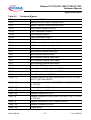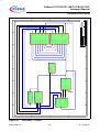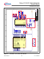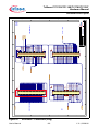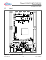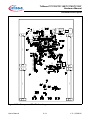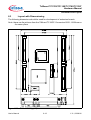
1
32-Bit
Microcontroller
TriBoard
TC176X/TC116X/TC1782/
TC1387
Hardware: TriBoard-LQFP176 V2.1
Hardware Manual
User’s Manual
V 2.1 2009-06
Microcontrollers
Edition 2009-06
Published by
Infineon Technologies AG
81726 Munich, Germany
© 2009 Infineon Technologies AG
All Rights Reserved.
Legal Disclaimer
The information given in this document shall in no event be regarded as a guarantee of conditions or
characteristics. With respect to any examples or hints given herein, any typical values stated herein and/or any
information regarding the application of the device, Infineon Technologies hereby disclaims any and all warranties
and liabilities of any kind, including without limitation, warranties of non-infringement of intellectual property rights
of any third party.
Information
For further information on technology, delivery terms and conditions and prices, please contact the nearest
Infineon Technologies Office (www.infineon.com).
Warnings
Due to technical requirements, components may contain dangerous substances. For information on the types in
question, please contact the nearest Infineon Technologies Office.
Infineon Technologies components may be used in life-support devices or systems only with the express written
approval of Infineon Technologies, if a failure of such components can reasonably be expected to cause the failure
of that life-support device or system or to affect the safety or effectiveness of that device or system. Life support
devices or systems are intended to be implanted in the human body or to support and/or maintain and sustain
and/or protect human life. If they fail, it is reasonable to assume that the health of the user or other persons may
be endangered.
32-Bit
Microcontroller
TriBoard
TC176X/TC116X/TC1782/
TC1387
User’s Manual
V 2.1 2009-06
Microcontrollers
TriBoard TC176X/TC116X/TC1782/TC1387
Hardware Manual
TriBoard TC176X/TC116X/TC1782/TC1387 User’s Manual
Revision History: V 2.1 2009-06
Previous Versions: TriBoardManual-TC176X-TC116X-TC1782-TC1387 V2.0
Page
Subjects (major changes since last revision)
–
change to actual manual template
–
add support for 1,3V VDD incl. updated schematic
Trademarks
TriCore® is a trademark of Infineon Technologies AG.
We Listen to Your Comments
Any information within this document that you feel is wrong, unclear or missing at all?
Your feedback will help us to continuously improve the quality of this document.
Please send your proposal (including a reference to this document) to:
[email protected]
User’s Manual
V 2.1, 2009-06
TriBoard TC176X/TC116X/TC1782/TC1387
Hardware Manual
Table of Contents
1
Introduction . . . . . . . . . . . . . . . . . . . . . . . . . . . . . . . . . . . . . . . . . . . . . . 1-1
2
2.1
2.2
2.3
TriBoard Features . . . . . . . . . . . . . . . . . . . . . . . . . . . . . . . . . . . . . . . . .
Summary of Features . . . . . . . . . . . . . . . . . . . . . . . . . . . . . . . . . . . . . . .
Block Diagram . . . . . . . . . . . . . . . . . . . . . . . . . . . . . . . . . . . . . . . . . . . . .
Placement . . . . . . . . . . . . . . . . . . . . . . . . . . . . . . . . . . . . . . . . . . . . . . . .
2-1
2-1
2-3
2-4
3
3.1
3.2
3.3
3.4
3.4.1
3.4.2
3.5
3.5.1
3.6
3.7
3.8
3.9
3.10
3.11
3.11.1
3.11.2
TriBoard Information . . . . . . . . . . . . . . . . . . . . . . . . . . . . . . . . . . . . . . .
Power Supply . . . . . . . . . . . . . . . . . . . . . . . . . . . . . . . . . . . . . . . . . . . . . .
LEDs . . . . . . . . . . . . . . . . . . . . . . . . . . . . . . . . . . . . . . . . . . . . . . . . . . . .
Clock . . . . . . . . . . . . . . . . . . . . . . . . . . . . . . . . . . . . . . . . . . . . . . . . . . . .
USB Connector . . . . . . . . . . . . . . . . . . . . . . . . . . . . . . . . . . . . . . . . . . . .
Serial Connection to PC . . . . . . . . . . . . . . . . . . . . . . . . . . . . . . . . . . .
MiniWiggler . . . . . . . . . . . . . . . . . . . . . . . . . . . . . . . . . . . . . . . . . . . . .
FlexRay / IFlex (optional if not with TC1767, TC1782 or TC1387) . . . . .
FlexRay as option . . . . . . . . . . . . . . . . . . . . . . . . . . . . . . . . . . . . . . . .
Serial Eeprom . . . . . . . . . . . . . . . . . . . . . . . . . . . . . . . . . . . . . . . . . . . . .
MultiCAN . . . . . . . . . . . . . . . . . . . . . . . . . . . . . . . . . . . . . . . . . . . . . . . . .
Safety option with SAK-CIC61508 (optional if not with TC1387) . . . . . . .
Other peripherals . . . . . . . . . . . . . . . . . . . . . . . . . . . . . . . . . . . . . . . . . . .
Toggle LED’s . . . . . . . . . . . . . . . . . . . . . . . . . . . . . . . . . . . . . . . . . . . . . .
Debug System . . . . . . . . . . . . . . . . . . . . . . . . . . . . . . . . . . . . . . . . . . . . .
OCDS1 . . . . . . . . . . . . . . . . . . . . . . . . . . . . . . . . . . . . . . . . . . . . . . . .
DAP . . . . . . . . . . . . . . . . . . . . . . . . . . . . . . . . . . . . . . . . . . . . . . . . . . .
3-1
3-1
3-1
3-1
3-2
3-2
3-2
3-3
3-3
3-3
3-3
3-4
3-4
3-4
3-4
3-4
3-5
4
4.1
4.2
4.3
TriBoard Configuration . . . . . . . . . . . . . . . . . . . . . . . . . . . . . . . . . . . . .
HW Boot Configuration TC1767, TC1782 and TC1387 . . . . . . . . . . . . . .
HW Boot Configuration all other TC176X / TC116X . . . . . . . . . . . . . . . .
Assembly Options . . . . . . . . . . . . . . . . . . . . . . . . . . . . . . . . . . . . . . . . . .
4-1
4-1
4-2
4-4
5
5.1
5.2
5.3
TriBoard Software . . . . . . . . . . . . . . . . . . . . . . . . . . . . . . . . . . . . . . . . .
Requirements . . . . . . . . . . . . . . . . . . . . . . . . . . . . . . . . . . . . . . . . . . . . .
Software Overview . . . . . . . . . . . . . . . . . . . . . . . . . . . . . . . . . . . . . . . . . .
Software Installation . . . . . . . . . . . . . . . . . . . . . . . . . . . . . . . . . . . . . . . .
5-1
5-1
5-1
5-1
6
Signal Description . . . . . . . . . . . . . . . . . . . . . . . . . . . . . . . . . . . . . . . . . 6-1
7
7.1
7.2
7.3
7.4
7.5
Connector Pin Assignment . . . . . . . . . . . . . . . . . . . . . . . . . . . . . . . . . .
TC176X/TC116X Connector / Top View . . . . . . . . . . . . . . . . . . . . . . . . .
Power connector pinout . . . . . . . . . . . . . . . . . . . . . . . . . . . . . . . . . . . . . .
USB connector pinout . . . . . . . . . . . . . . . . . . . . . . . . . . . . . . . . . . . . . . .
Flexray Pinout . . . . . . . . . . . . . . . . . . . . . . . . . . . . . . . . . . . . . . . . . . . . .
CAN connector pinout . . . . . . . . . . . . . . . . . . . . . . . . . . . . . . . . . . . . . . .
User’s Manual
L-1
7-1
7-2
7-4
7-4
7-4
7-5
V 2.1, 2009-06
TriBoard TC176X/TC116X/TC1782/TC1387
Hardware Manual
7.6
7.7
OCDS connector pinout . . . . . . . . . . . . . . . . . . . . . . . . . . . . . . . . . . . . . . 7-5
DAP connector pinout (only with TC1767, TC1782, TC1387) . . . . . . . . . 7-5
8
8.1
8.1.1
Schematic and Layout . . . . . . . . . . . . . . . . . . . . . . . . . . . . . . . . . . . . . . 8-1
Schematic . . . . . . . . . . . . . . . . . . . . . . . . . . . . . . . . . . . . . . . . . . . . . . . . 8-1
New and changes on schematic version V2.1 to TriBoard
TC176X/TC116X/TC1782/TC1387 V2.0 8-1
Layout . . . . . . . . . . . . . . . . . . . . . . . . . . . . . . . . . . . . . . . . . . . . . . . . . . 8-10
Layout with Dimensioning . . . . . . . . . . . . . . . . . . . . . . . . . . . . . . . . . . . 8-12
8.2
8.3
User’s Manual
L-2
V 2.1, 2009-06
TriBoard TC176X/TC116X/TC1782/TC1387
Hardware Manual
List of Figures
Figure 2-1
Figure 2-2
Figure 3-1
Figure 4-1
Figure 4-2
Figure 4-3
Figure 4-4
Figure 4-5
Figure 4-6
Figure 4-7
Figure 7-1
Figure 7-2
Figure 7-3
Figure 7-4
Figure 7-5
Figure 7-6
Figure 7-7
Figure 7-8
Figure 8-1
Figure 8-2
Figure 8-3
Figure 8-4
Figure 8-5
Figure 8-6
Figure 8-7
Figure 8-8
Figure 8-9
Figure 8-10
Figure 8-11
Figure 8-12
User’s Manual
TriBoard Block Schematic . . . . . . . . . . . . . . . . . . . . . . . . . . . . . . . . . 2-3
TriBoard LQFP176 V2.1 Placement . . . . . . . . . . . . . . . . . . . . . . . . . 2-4
Clock socket usage (XT301) . . . . . . . . . . . . . . . . . . . . . . . . . . . . . . . 3-2
HW Configuration TC1767, TC1782, TC1387 DIP-Switch. . . . . . . . . 4-1
HW Configuration for all other TC176X / TC116X DIP-Switch. . . . . . 4-2
Location of general optional resistors on Top Side . . . . . . . . . . . . . . 4-5
Location of general optional resistors on Bottom Side. . . . . . . . . . . . 4-5
Location of peripheral resistors on Top Side . . . . . . . . . . . . . . . . . . . 4-7
Location of peripheral resistors on Bottom Side . . . . . . . . . . . . . . . . 4-7
Location of resistors for safety device on Bottom Side . . . . . . . . . . . 4-8
Connector for TC176X/TC116X/TC1782/TC1387 - Pinout (Part I, Top
View) 7-2
Connector for TC176X/TC116X/TC1782/TC1387 - Pinout (Part II, Top
View) 7-3
Power connector pinout . . . . . . . . . . . . . . . . . . . . . . . . . . . . . . . . . . . 7-4
USB connector Pinout . . . . . . . . . . . . . . . . . . . . . . . . . . . . . . . . . . . . 7-4
Flexray Pinout (SUBD-9 Plug) . . . . . . . . . . . . . . . . . . . . . . . . . . . . . . 7-4
CAN connector pinout (IDC10) . . . . . . . . . . . . . . . . . . . . . . . . . . . . . 7-5
OCDS connector pinout (IDC16) . . . . . . . . . . . . . . . . . . . . . . . . . . . . 7-5
DAP connector pinout (FTSH10) - only with TC1767, TC1782, TC1387. .
7-5
Schematic - Project . . . . . . . . . . . . . . . . . . . . . . . . . . . . . . . . . . . . . . 8-2
Schematic - Config, Clock and CIC61508 . . . . . . . . . . . . . . . . . . . . . 8-3
Schematic - IFlex, CAN and Eeprom . . . . . . . . . . . . . . . . . . . . . . . . . 8-4
Schematic - MiniWiggler, DAP and ETK . . . . . . . . . . . . . . . . . . . . . . 8-5
Schematic - GPTA, MSC, MLI and ADC . . . . . . . . . . . . . . . . . . . . . . 8-6
Schematic - Power Supply . . . . . . . . . . . . . . . . . . . . . . . . . . . . . . . . . 8-7
Schematic - Connectors (Plug) . . . . . . . . . . . . . . . . . . . . . . . . . . . . . 8-8
Schematic - Connectors (Socket) . . . . . . . . . . . . . . . . . . . . . . . . . . . 8-9
Component Plot Top Layer . . . . . . . . . . . . . . . . . . . . . . . . . . . . . . . 8-10
Component Plot Bottom Layer . . . . . . . . . . . . . . . . . . . . . . . . . . . . . 8-11
Dimensioning (mil) . . . . . . . . . . . . . . . . . . . . . . . . . . . . . . . . . . . . . . 8-12
Dimensioning (mm) . . . . . . . . . . . . . . . . . . . . . . . . . . . . . . . . . . . . . 8-13
L-3
V 2.1, 2009-06
TriBoard TC176X/TC116X/TC1782/TC1387
Hardware Manual
User’s Manual
L-4
V 2.1, 2009-06
TriBoard TC176X/TC116X/TC1782/TC1387
Hardware Manual
List of Tables
Table 4-1
Table 4-2
Table 4-3
Table 4-4
Table 4-5
Table 6-1
Table 6-2
Table 6-3
Table 6-4
Table 6-5
Table 6-6
Table 6-7
User’s Manual
User Startup Modes for TC1767, TC1782 and TC1387 . . . . . . . . . .
HW Boot Configuration for all other TC176X / TC116X . . . . . . . . . . .
General optional resistors . . . . . . . . . . . . . . . . . . . . . . . . . . . . . . . . .
Resistors for peripherals . . . . . . . . . . . . . . . . . . . . . . . . . . . . . . . . . .
Resistors for safety device . . . . . . . . . . . . . . . . . . . . . . . . . . . . . . . . .
Power Signals . . . . . . . . . . . . . . . . . . . . . . . . . . . . . . . . . . . . . . . . . .
Reset Signals. . . . . . . . . . . . . . . . . . . . . . . . . . . . . . . . . . . . . . . . . . .
Interrupt Signals. . . . . . . . . . . . . . . . . . . . . . . . . . . . . . . . . . . . . . . . .
Clock Signals . . . . . . . . . . . . . . . . . . . . . . . . . . . . . . . . . . . . . . . . . . .
Debug Signals . . . . . . . . . . . . . . . . . . . . . . . . . . . . . . . . . . . . . . . . . .
Peripheral Signals . . . . . . . . . . . . . . . . . . . . . . . . . . . . . . . . . . . . . . .
Safety device Signals. . . . . . . . . . . . . . . . . . . . . . . . . . . . . . . . . . . . .
L-5
4-1
4-2
4-4
4-6
4-8
6-1
6-1
6-2
6-2
6-2
6-2
6-4
V 2.1, 2009-06
TriBoard TC176X/TC116X/TC1782/TC1387
Hardware Manual
User’s Manual
L-6
V 2.1, 2009-06
TriBoard TC176X/TC116X/TC1782/TC1387
Hardware Manual
User’s Manual
-7
V 2.1, 2009-06
TriBoard TC176X/TC116X/TC1782/TC1387
Hardware Manual
Introduction
1
Introduction
We congratulate you on your purchase of the TriCore Evaluation Board. This kit is a
versatile tool, providing quick access to the capabilities of TriCore's powerful
architecture.
Applications can be developed easily. The Evaluation Board is equipped with a variety
of memories and peripherals for connection to the environment. There is also an
interface for the On Chip Debugging Features (OCDS1 and DAP). The kit also includes
several sets of development tools, which are stored on the included Evaluation Board
CD-ROM.
The Evaluation Board allows easily the development of TriCore applications with the
corresponding tools.
Subsequently, the applications can be downloaded and can be tested with the powerful
debugger software.
This TriBoard Hardware Manual familiarizes you with the TriCore Evaluation Board and
guides you through the initial configuration of the TriBoard.
For detailed technical information about the TC176X / TC116X / TC1782 / TC1387
please refer to the User Manual of the corresponding device.
User’s Manual
1-1
V 2.1, 2009-06
TriBoard TC176X/TC116X/TC1782/TC1387
Hardware Manual
Introduction
User’s Manual
1-2
V 2.1, 2009-06
TriBoard TC176X/TC116X/TC1782/TC1387
Hardware Manual
TriBoard Features
2
TriBoard Features
The TriBoard TC176X/TC116X/TC1782/TC1387 is soldered with a device of the
TC176X or TC116X or TC1782 or TC1387. This devices fits into all members of this
product family so that there are no special TriBoards necessary.
2.1
–
–
–
–
–
–
–
–
–
–
–
Summary of Features
Infineon’s TC176X, TC116X, TC1782 or TC1387 Controller in LQFP176 Package
FlexRay Transceivers (optional if not with TC1767 or TC1782 or TC1387)
Safety device (optional if not with TC1387)
High Speed CAN Transceivers
USB to UART bridge
Crystal 20MHz (default), Oscillator or External Clock
USB miniWiggler for easy debugging
8 Low Power Status LEDs
8-DIP switches for configuration
access to all pins of controller
100mm x 160mm (EURO-Board)
Connectors
The TC176X / TC116X / TC1782 / TC1387 TriBoard offers a wide variety of connectors:
–
–
–
–
–
–
Standard power connector
USB connector for ASC Interface (ASC0) and miniWiggler
16-pin header for JTAG interface (OCDS)
10-pin header for DAP (only TC1767, TC1782, TC1387)
2 x 10pin (2x5) Header for CAN High Speed Transceiver (CAN0 and CAN1)
2 x SUB-D9 Plug connector for FlexRay (optional if not with TC1767, TC1782,
TC1387)
– four 80-pin connectors (male) + four 80-pin connectors (female) with all I/O signals
– optional ETK connector
Components
–
–
–
–
–
–
Infineon’s Next generation micro controller supply TLE 7368 G
Three LEDs to validate power supply (5Volt / 3,3 Volt / VCORE)
LED indicating /HDRST (ESR0) active state
LED indicating activ miniWiggler
LED switched via DAS software
Infineon’s FlexRay Communication Controller SAK-CIC310 (optional if not with
TC1767, TC1782, TC1387)
– 2x FlexRay Transceiver AS8221(AMS) or TJA1080 (NXP) (optional if not with
TC1767, TC1782, TC1387)
– 2 x Infineon’s High Speed CAN-Transceiver TLE 6250 GV33
– Infineon’s Safety Device SAK-CIC61508(optional if not with TC1387)
User’s Manual
2-1
V 2.1, 2009-06
TriBoard TC176X/TC116X/TC1782/TC1387
Hardware Manual
TriBoard Features
–
–
–
–
–
USB to UART bridge FT2232D (FTDI)
SPI eeprom (Atmel)
8 general purpose LEDs
Reset switch
8-pin Dip switch
Zero Ohm Bridges
Zero Ohm resistors give the flexibility to configure the systems functionality
User’s Manual
2-2
V 2.1, 2009-06
TriBoard TC176X/TC116X/TC1782/TC1387
Hardware Manual
TriBoard Features
2.2
Block Diagram
XTAL
CAN0
RxCAN0
CAN1
PLL
TxCAN0
Transceiver
TxCAN1
RxCAN1
TC176X /
TC116X /
TC1782 /
TC1387
OCDS1
miniWiggler
ERAY A
FlexRay only with TC1767,
TC1782 and TC1387
for other devices optional
ERAY B
FlexRay
Transceiver
Figure 2-1
User’s Manual
MLI0
RXD0
8 LED’s
(P5.0 up to P5.7)
SAKCIC310
SLSO00
TriCore
CPU
TXD0
SSC0
USB
SSC1
USB
B-TYPE
Serial EEPROM
Safety Device
SAK-CIC61508
optional if not with TC1387
POWER SUPPLY WITH
SUPERSONIC
TLE7368G / TLE7368-2G
TriBoard Block Schematic
2-3
V 2.1, 2009-06
TriBoard TC176X/TC116X/TC1782/TC1387
Hardware Manual
TriBoard Features
2.3
Placement
USB
P401
RUN
1
X202
1 2 3 4 5 6 7 8
XT201
S201
1
DAP
VDDP_CIC
1
OCDS1
R249
X402
SYSDISC
BOOTCONFIG
ACT
SYSDISB
X403 A1
1
X203
OCDS1_CIC
P5.0 P5.1 P5.2 P5.3 P5.4 P5.5 P5.6 P5.7
ETK
ERAY-A
X701
1
1
SYSDISA
X704
1
1
SEND
Figure 2-2
User’s Manual
R245
U601
JP201
R242
SENC
R237
1
SENB
RST_CIC
SENA
S202
RESET_CIC
X703
+5,5V...+50V(+40V)
X201
TC176X/TC116X/
TC1782/TC1387
+VDD
JP202
SAK-CIC61508
JP203
+3V3
1
+5V
U202
1
X302
RST
X601
SUPERSONIC
S601
CAN1
P302
U201
1
RESET
POWER
TriBoard-LQFP176 V2.1
ERAY-B
X301
X401
1
CAN0
L1
1
P301
CLOCK
X702
1
1
1
1
TriBoard LQFP176 V2.1 Placement
2-4
V 2.1, 2009-06
TriBoard TC176X/TC116X/TC1782/TC1387
Hardware Manual
TriBoard Information
3
TriBoard Information
3.1
Power Supply
The Board has to be connected to a +5,5V to +50V (+40V) DC power supply. The
TriBoard generates internally +3.3V, +VDD and +5V. The power consumption is not
specified yet but a supply with 6V and 500mA should be sufficient. The pinout for the
supply connector is shown in Figure 7-3. There can be used any standard power pack
with a connector where the positive line is surrounded by the ground line.
Maximum power supply is reduced to +40V if the SAK-CIC61508 option is assembled
(always with TC1387).
+VDD is +1,3V for TC1782, for all other devices +1,5V. NOTE: on first TC1782 device
+VDD is +1,2V.
Applying a stable supply voltage causes the power on reset after a short period. The four
LED's (+5V, +3.3V, +VDD) indicate the status of the on board generated voltage (if the
LEDs are assembled).
A manual reset is executed by pressing the reset button.
3.2
LEDs
There are 14 or 19 LEDs on board:
–
–
–
–
–
–
–
–
–
–
–
–
3.3
D501 up to D508 (blue)
D604 RST (red)
D505 +VDD (green)
D606 +3V3 (green)
D607 +5V (green)
D402 ACT (green)
D401 RUN (red)
D204 RST_CIC (red)
D205 +VDDP_CIC (green)
D201 SYSDISA (red)
D202 SYSDISB (red)
D203 SYSDISC (red)
-> toogle LEDs connected to P5.0 ... P5.7
-> RESET LED indicate the reset state of the board
-> +VDD power supply indication (+1.3V/+1.5V)
-> +3,3V power supply indication
-> +5V power supply indication
-> on board MiniWiggler is ACTIV
-> Debug RUN mode (switched by DAS Server)
-> RESET LED indicate that the CIC is in reset
-> +VDDP for CIC power supply indication (+3,3V)
-> System Disable A (switched by CIC)
-> System Disable B (switched by CIC)
-> System Disable C (switched by CIC)
Clock
There are three possibilities to apply the CPU clock.
•
•
•
•
Large oscillator circuit (DIP14)
Small oscillator circuit (DIP8)
Crystal oscillator (default with 20MHz)
External clock generator
User’s Manual
3-1
V 2.1, 2009-06
TriBoard TC176X/TC116X/TC1782/TC1387
Hardware Manual
TriBoard Information
The crystal oscillator and the oscillator circuit use the socket XT301. It's possible to apply
a 14pol DIP oscillator package or an 8pol DIP oscillator package.
OSCILLATOR
OSCILLATOR
XTAL
DIP14
DIP8
Figure 3-1
3.4
GND
External
Clock Input
Clock socket usage (XT301)
USB Connector
The USB connector is used for connection to a PC. Via the USB it is possible to power
the board, using the ASC0 as serial connection via USB and Debugging via DAS. For
the pinout of USB socket see Figure 7-4.
NOTE: Before connecting the board to the PC, make sure that the actual DAS software
is installed on the PC. For actual DAS software please contact your local FAE.
The software can also be found on the
DAS website
3.4.1
Serial Connection to PC
After the first connection of USB to a PC the needed driver will be installed automatically.
During this there will be created a new COM port on PC. This COM port can be used to
communicate with the board via ASC0 of the device (e.g. bootstrap loader).
3.4.2
MiniWiggler
MiniWiggler is a low cost debug tool which allows you access to the JTAG of the device.
Make sure that you have the latest DAS release. Debugging is possible via the DAS
Server JTAG over USB Chip. Please contact your prefered debug vendor for support of
DAS.
If you have connected the board to the PC and there runs the DAS server, then a working
connection is visible via the green ACTIV LED.
The status RUN LED is switched on/off through the DAS Server, depending on the used
debugger (client).
User’s Manual
3-2
V 2.1, 2009-06
TriBoard TC176X/TC116X/TC1782/TC1387
Hardware Manual
TriBoard Information
IMPORTANT: Make sure that there is no or a tristated connection on X401 (OCDS1) and
X402 (DAP) if the ACTIV LED is on.
3.5
FlexRay / IFlex (optional if not with TC1767, TC1782 or TC1387)
The FlexRay devices are only assembled if the board is with TC1767, TC1782, TC1387
or with the FlexRay option.
The board has 2 SUB-D connectors for FlexRay Communication with up to 10 Mbit/s.
For the pinout of the plugs see Figure 7-5.
The transceiver are connected to the FlexRay Communication Controller SAK-CIC310
(IFlex).
Normally the SAK-CIC310 is connected to MLI0 of the TriCore Controller but the IFlex
can also be connected to SSC1.For using the IFlex with SSC see Table 4-4. As
interrupts inputs of TC176X/TC116X are used P0.7, P0.11, P3.10 and P3.11 and in case
of SSC1 connection you can also use P0.6.
For more information look in the user manual for TC176X/TC116X or SAK-CIC310 and
the schematics Figure 8-4.
3.5.1
FlexRay as option
If the board comes without FlexRay (e.g. with TC1766) then you can add the FlexRay
option by assembling the following parts:
•
•
•
•
U301 with SAK-CIC310 (Infineon)
U302 and U303 with AS8221 (AMS) or TJA1080 (NXP) (if with TJA1080 then
resistors R366-R371 and capacitor CB312 and CB316 must be assembled with 0R
and 100n, package 0603)
Y301 with 20MHz crystal (5x3mm SMD, e.g. NDK NX5032GA)
T301 and T302 with B82790-S513-N (Epcos)
3.6
Serial Eeprom
The SSC0 of the TC176X / TC116X / TC1782 / TC1387 is connected to a serial
EEPROM with a size of 128K (16.384 x 8). As chip select for this EEPROM is used the
line SLSO00 (P3.5). To disconnect (disable) the EEPROM remove resistor R353.
3.7
MultiCAN
On the board are two CAN transceiver connected to the MultiCAN on TC176X / TC116X
/ TC1782 / TC1387 node 0 and 1. The transceivers are connected to two IDC10 plug.
For the pinout of IDC10 plug see Figure 7-6. You can use a IDC female connector with
crimpconnector, flat cable and SUB-D 9 plug with crimpconnector to have a 1:1 adapter
to SUB-D 9.
User’s Manual
3-3
V 2.1, 2009-06
TriBoard TC176X/TC116X/TC1782/TC1387
Hardware Manual
TriBoard Information
3.8
Safety option with SAK-CIC61508 (optional if not with TC1387)
The safety device is only assembled if the board is with TC1387 or with the safety option.
The SAK-CIC61508 is connected to the SSC0 of the microcontroller and use the line
SLSO01 (P3.6) as chip select.
There are 4 LED’s for indication the state of the safety device (SYSDISA, SYSDISB,
SYSDISC, VDDP_CIC).
On this board exists 4 potentiometer to stimulare the sense inputs of the safety device.
Sensor inputs A and B can be connect to a potentiometer (JP201, JP202 , pos. 2-3) or
to the core voltage of the microcontroller (JP201, pos. 1-2) for input A or to the port
voltage of the microcontroller (JP202, pos. 1-2) for input B.
With switch S202 it is possible to reset the safety device. If JP203 is set, then with S202
is also reset the microcontroller and the safety device is reset by a power on reset of the
microcontroller.
The safety device can be reprogrammed via JTAG and X203.
3.9
Other peripherals
For all other peripherals there are no special plugs on the board. The peripheral signals
are available on the different connectors. See “Connector Pin Assignment” on
Page 7-1.
Note: - SLSO00 is used as chip select for the serial eeprom on board.
3.10
Toggle LED’s
Port 5 pin 0 up to pin 7 are connected to single LED’s (D501... D508) and can be
controlled by Software. This status LED’s are low active.
3.11
Debug System
3.11.1
OCDS1
The OCDS1 signals are connected to the IDC16 plug (X401). They work with the port
supply of +3.3V. For pinout of the connector see Figure 7-7. You can connect any
debugger to this connector.
The signals /BRKIN and /BRKOUT are not connected per default. If you need this signals
in the connector then assemble R425 and R424 with a 0R resistor.
If you connect a debug hardware make sure that the MiniWiggler (see “MiniWiggler”
on Page 3-2) is not activ (ACTIV LED is off) and on the DAP connector (X402) is no
hardware connected or the hardware is tristated.
User’s Manual
3-4
V 2.1, 2009-06
TriBoard TC176X/TC116X/TC1782/TC1387
Hardware Manual
TriBoard Information
If the ACTIV LED is on, then stop the active DAS Server JTAG over USB Chip and/or
remove the USB connection to the PC.
3.11.2
DAP
If the board comes with a TC1767, TC1782 or TC1387 then the DAP connector (X402)
is available. For pinout of this connector see Figure 7-8. You can connect a DAP
hardware here. If you use this connector make sure that the MiniWiggler is not activ
(ACTIV LED is off) and a connected OCDS1 hardware is disconnected or tristated.
User’s Manual
3-5
V 2.1, 2009-06
TriBoard TC176X/TC116X/TC1782/TC1387
Hardware Manual
TriBoard Information
User’s Manual
3-6
V 2.1, 2009-06
TriBoard TC176X/TC116X/TC1782/TC1387
Hardware Manual
HW Boot Configuration TC1767, TC1782 and TC1387
Figure 4-1
P0
.
P0
.5
.4
P0
P0
.2
P0
.1
P0
0
HIGH 1
P0
.
LOW
P0
.
4.1
6
TriBoard Configuration
.3
4
7
TriBoard Configuration
on
2
3
4
5
6
7
8
HW Configuration TC1767, TC1782, TC1387 DIP-Switch
The picture above shows the definition of the boot HW configuration switch. The
meaning of the switches will be described in the following table (Table 4-1).
Note: The ON position of the switch is equal to a logical LOW at the dedicated pin.
Table 4-1
User Startup Modes for TC1767, TC1782 and TC1387
Note: The shadowed line indicates the default setting.
Note: ’x’ represents the don’t care state.
Note: 1 to 8 are the Dip Switch numbers
HWCFG[7...0] Type of Boot TC1767, TC1782 and TC1387
1 2 3 4 5 6 7 8
11XXXXXX
Internal Start from Flash
X X X X X X O O
F F
F F
010XXXX0
Bootstrap Loader Mode, Generic Bootloader at O X X X X O O O
CAN pins
N
N F N
F
10101XX0
Bootstrap Loader Mode, ASC Bootloader
O X X O O O O O
N
F N F N F
F
F
F
10100XX0
Alternate Boot Mode, ASC Bootloader on fail
O X X O O O O O
N
N N F N F
F
F
User’s Manual
4-1
V 2.1, 2009-06
TriBoard TC176X/TC116X/TC1782/TC1387
Hardware Manual
TriBoard Configuration
Table 4-1
User Startup Modes for TC1767, TC1782 and TC1387
Note: The shadowed line indicates the default setting.
Note: ’x’ represents the don’t care state.
Note: 1 to 8 are the Dip Switch numbers
HWCFG[7...0] Type of Boot TC1767, TC1782 and TC1387
1 2 3 4 5 6 7 8
1011XXXX
Alternate Boot Mode, Generic Bootloader at
CAN pins on fail
X X X X O O O O
F F N F
F
F F
all others
reserved; don’t use this combination
HIGH
7
P0
.
6
P0
.
P0
.5
P0
.4
P4
.3
P4
.2
LOW
P4
.1
HW Boot Configuration all other TC176X / TC116X
P4
.0
4.2
on
1
2
Figure 4-2
3
4
5
6
7
8
HW Configuration for all other TC176X / TC116X DIP-Switch
The picture above shows the definition of the boot HW configuration switch. The
meaning of the switches will be described in the following table (Table 4-2).
Note: The ON position of the switch is equal to a logical LOW at the dedicated pin.
Table 4-2
HW Boot Configuration for all other TC176X / TC116X
Note: The shadowed line indicates the default setting.
Note: ’x’ represents the don’t care state.
Note: 1 to 8 are the Dip Switch number
P4[3...0]
P0[7...4]
Type of Boot TC176X / TC116X
1 2 3 4 5 6 7 8
0000
XXXX
Serial boot from ASC to PMI
scratchpad via ASC pins, run loaded
program
O O O O X X X X
N N N N
0001
XXXX
Serial boot from CAN to PMI
scratchpad, run loaded program
O O O O X X X X
F N N N
F
User’s Manual
4-2
V 2.1, 2009-06
TriBoard TC176X/TC116X/TC1782/TC1387
Hardware Manual
TriBoard Configuration
Table 4-2
HW Boot Configuration for all other TC176X / TC116X
Note: The shadowed line indicates the default setting.
Note: ’x’ represents the don’t care state.
Note: 1 to 8 are the Dip Switch number
P4[3...0]
P0[7...4]
Type of Boot TC176X / TC116X
1 2 3 4 5 6 7 8
0010
XXXX
Start from internal flash
O O O O X X X X
N F N N
F
0011
XXXX
Alternate Boot Mode, Generic Boot
Loader on fail depends on P0[2...0]
O O O O X X X X
F F N N
F F
1000
XXXX
Boot from emulation memory (ED only)
O O O O X X X X
N N N F
F
1111
XXXX
Serial boot from ASC to PMI
scratchpad via CAN pins, run loaded
program
O O O O X X X X
F F F F
F F F F
all others all others reserved; don’t use this combination
User’s Manual
4-3
V 2.1, 2009-06
TriBoard TC176X/TC116X/TC1782/TC1387
Hardware Manual
TriBoard Configuration
4.3
Assembly Options
Table 4-3
General optional resistors
Component Description
R205
XTAL Rserial (default: assembled)
R206
XTAL Rparallel (default: not assembled)
R423
Connect /BRKOUT with MiniWiggler (default: not assembled)
R424
Connect /BRKOUT with OCDS1 connector (default: not assembled)
R427
Connect /BRKIN with USR1 of MiniWiggler (default: not assembled
R429
Connect /BRKIN with USR1 of DAP (default: not assembled
R425
Connect /BRKIN with OCDS1 connector(default: not assembled)
R428
Connect /TESTMODE with USR1 of MiniWiggler (default: not assembled
R430
Connect /TESTMODE with USR1 of DAP (default: not assembled
R426
Connect /TESTMODE with OCDS1 connector(default: not assembled)
R432
Connect debug reset with /PORST(default: assembled)
R431
Connect debug reset with /HDRST (default:not assembled)
R510
Connect +3,3V to all toggle LEDs (default: assembled)
R623
Connect reset switch with /PORST(default: assembled)
R624
Connect reset switch with /HDRST (default:not assembled)
R604
Connect P1.2 with MONSTBY of power device (default: not assembled)
R606
Connect P1.3 with WDO of power device (default: not assembled)
R609
Connect P1.15 with WDI of power device (default: not assembled)
User’s Manual
4-4
V 2.1, 2009-06
TriBoard TC176X/TC116X/TC1782/TC1387
Hardware Manual
TriBoard Configuration
Note: All resistors are red marked in the following figures
R407
X704
D205
R249
R245
R242
JP202
U203
X302
CB208
X201
R355
JP203
R228
C603
D606
D605
CB319
R601 R501
R237
R227
D607
R639
D204
U306
C610
C608
R603
D203
R235
D202
R234
R233
X202
S201
R510
R512
R322
R622
S601
L601
CB209
R353
R641
R607
R640
U202
R229
U601
R332
D201
X203
D508
D507
D506
D505
D504
D503
D501
D502
R308
U201
D604
CB601
R331
R330
P302
C304
C208
R431
CB314
R329
T302
R328
R371
CB204
CB207
JP201
R307
CB315
R325
R213
R231
R230
X301
R366
R432
R326
C607
1 2 3 4 5 6 7 8
XT201
R209
U204
R309
R312
CB309
U302
U303
CB316
R327
R515 R516 R517
R513 R514
R379
CB311
R311
R369
CB312
R323
R370
R321
R324
CB313
R511
CB404
CB402
C303
D401
T301
R367
R316
R317
R315
R314
P301
CB310
R518
R434
R433
R372
R310
R368
X403
X401
R439
R210
R313
R318
D403
D402
R408
X402
1
CB203
R405
C401
R401
X701
1
R406
L401
C207
U402
CB401
R621
R402
R403
R404
C602 C604
CB406
P401
S202
R356
R354
R608
R602
X601
C611
X703
1
Location of general optional resistors on Top Side
X801
X804
1
C618
U401
R412
U404
R423
R418
R609
CB301
CB307
Q602
R301
R623
R624
R606 R628
Q603 R627
D609
D602
C605
C609
R605
R616
D608
Q601
X803
1
User’s Manual
U301
CB305
R360
R620
X802
Figure 4-4
CB303
R346
CB304
R359
CB308
R303
R351 CB302
R348
CB306
R302
Q406 Q404 Q402
Q405 Q403 Q401
R338
R340
R344
U305
L301
L302
R349
C614
U603
R519
C301
R352
R350
R604
R617
R520
R429
C606
R619
R618
R507
R334
U304
R642
L602
CB629
R505
D603
R345
R411
R430
Y301
R638
R347
CB604
R613
R343
R319
C617
CB504
R342
R414
R424
C613
R644
R643
R438
Q604
R504
R437
CB318
R630
R502
R503
R509
CB503
CB506
CB508
R508
R529
R528
CB624 CB613
CB403
CB409
R416
R341
C615
R361
R320
Y401
CB408
R410
R335
R305
CB607
CB501
R440
R337
R333
R339
R523
R363
CB619
R527
R533 R534
CB502
R419
R365 R426
R626 R425
R336
R625
R306
CB317
R375
R634
R531
R530
CB608
C616
C204
C203
R205
R204
R358
CB605
CB614
CB620
R219
R216
R215
R221
CB610
CB602
CB626
CB202
CB612
R373
R378
R417
CB405
U403
C612
CB625
R254
R635
R532
R526
R629
R253
R236
R631
C201 CB621
R615
R636 CB606
CB617
R633
R611
R632
R610
R256
R255
R238
CB609
R202
R374
U602
R258
R376
R377
R612
CB507
R201
R362
R637
CB201
R257
R427 CB407
R415
R409
R420
R206
CB603
C202
Y201
R241
R208
R364
R436
R422
R428
R357
R211
C206
R243
CB615
CB206
C205
CB205
R252
Y202
R240
R239
R244
R207
R212
R247
CB622
C212
R246
R203
R304
R614
C209
R220
R521
C210
R217
C211
R248
R218
R224
R222
R251
R223
R250
R225
R522
R525
R226
R232
R435
R524
R421
1
C302
Figure 4-3
X702
1
C601
1
D601
Location of general optional resistors on Bottom Side
4-5
V 2.1, 2009-06
TriBoard TC176X/TC116X/TC1782/TC1387
Hardware Manual
TriBoard Configuration
Table 4-4
Resistors for peripherals
Component Description
R333
Connect P3.12 with RXD of CAN0 transceiver (default: assembled)
R339
Connect P3.14 with RXD of CAN1 transceiver (default: assembled)
R353
Connect P3.5 (SLSO00) with /CS of Eeprom (default: assembled)
R345
Connect P2.3 (MLI0) with IFlex (default: assembled)
R346
Connect P2.0 (MLI0) with IFlex (default: assembled)
R347
Connect P2.2 (MLI0) with IFlex (default: assembled)
R348
Connect P2.1 (MLI0) with IFlex (default: assembled)
R349
Connect P2.7 (MLI0) with IFlex (default: assembled)
R350
Connect P2.4 (MLI0) with IFlex (default: assembled)
R351
Connect P2.6 (MLI0) with IFlex (default: assembled)
R352
Connect P2.5 (MLI0) with IFlex (default: assembled)
R357
Connect P2.12 (SSC1) with IFlex (default: not assembled)
R358
Connect P2.10 (SSC1) with IFlex (default: not assembled)
R359
Connect P3.6 (SSC1) with IFlex (default: not assembled)
R361
Connect P2.11 (SSC1) with IFlex (default: not assembled)
R360
Connect P0.6 (REQ2) with IFlex (default: not assembled)
R440
Connect P3.0 with TXD of USB to UART (default: assembled)
R505
Connect VAREF0 with VDDM (default: assembled)
R507
Connect VAGND0 with VSSM (default: assembled)
R508
Connect VFAREF with VDDMF (default: assembled if not with TC1387)
R509
Connect VFAGND with VSSMF (default: assembled if not with TC1387)
R519
Connect +5V with VDDM (default: assembled on TC1767, TC1782 and
TC1387)
R520
Connect +3,3V with VDDM (default: assembled if not TC1767, TC1782
or TC1387)
User’s Manual
4-6
V 2.1, 2009-06
TriBoard TC176X/TC116X/TC1782/TC1387
Hardware Manual
TriBoard Configuration
Note: All resistors are red marked in the following figures
R407
X704
U601
D205
R249
R245
JP202
U203
R639
CB319
R237
R355
JP203
R601 R501
D204
U306
C610
C608
X201
D606
D605
R228
C603
R229
R603
D203
R235
D202
R234
R233
X202
S201
R510
R512
R227
D607
JP201
R622
S601
D201
X203
D508
D507
D506
D505
D504
D503
D501
X302
CB209
R353
R641
R607
R640
U202
CB208
D604
CB601
R331
R332
L601
R330
P302
D502
R308
U201
R322
R312
CB315
R325
C304
C208
R431
CB314
R329
T302
R328
R371
CB204
CB207
R242
R432
R213
R231
R230
X301
R307
R309
R326
C607
1 2 3 4 5 6 7 8
XT201
R209
U204
R366
T301
R367
CB309
U302
U303
CB316
R327
R515 R516 R517
R513 R514
R379
CB311
R311
R369
CB312
R323
R370
R321
R324
CB313
R511
CB404
CB402
C303
D401
R317
R316
R315
R314
P301
CB310
R518
R434
R433
R372
R310
R368
X403
X401
R439
R210
R313
R318
D403
D402
R408
X402
1
CB203
R405
C401
R401
X701
1
R406
L401
C207
U402
CB401
C602 C604
R402
R403
R404
R621
CB406
P401
S202
R356
R354
R608
R602
X601
C611
X703
1
Location of peripheral resistors on Top Side
X801
X804
1
U401
R412
U404
R423
R418
R609
CB301
CB307
U301
CB303
R346
CB305
R360
Q602
CB304
R359
CB308
R303
R351 CB302
R348
CB306
R301
R623
R624
R606 R628
Q603 R627
D609
D602
C605
C609
R605
R616
D608
R302
Q406 Q404 Q402
Q405 Q403 Q401
R338
R334
R340
R344
U305
L301
L302
R349
Q601
X802
X803
1
User’s Manual
C301
R352
R620
Figure 4-6
R429
Y301
C606
C618
R430
C614
R519
R411
R350
R604
R617
R520
R424
R638
U603
R507
L602
R505
CB629
D603
R619
R618
CB604
R613
U304
R642
C617
CB504
R345
R414
R341
C615
R347
R416
C613
R644
R643
R319
CB403
CB409
R410
R335
R440
R337
R504
R342
Q604
R509
CB503
R508
CB506
CB508
R438
R343
R502
R503
CB501
Y401
CB408
R437
CB318
R630
CB624 CB613
CB317
R361
R320
R339
R523
R634
R531
R305
CB607
R527
R533 R534
CB502
R333
CB619
R529
R528
R530
CB608
C616
C204
R205
R204
C203
R215
R358
CB605
CB620
R219
R216
R221
CB610
CB602
CB626
CB202
CB612
R363
CB405
U403
C612
CB625
R254
R635
R532
R526
R629
R253
R236
R631
C201 CB621
R615
R636 CB606
CB617
CB507
CB609
R633
R611
R632
R610
R256
R255
R238
R375
U602
R258
R378
R637
CB201
R257
R427 CB407
R201
R417
R362
R202
R419
R376
R365 R426
R374 R626 R425
R336
R373 R306
R625
R377
R612
CB603
C202
Y201
R241
R208
R428
R206
R211
C206
R243
CB615
CB206
C205
R252
Y202
CB205
R240
R239
R244
R207
R212
R247
CB622
C212
R246
R364
R436
R422
R415
R409
R420
R357
R304
R614
C209
R203
CB614
R521
C210
R220
R218
C211
R248
R217
R222
R223
R251
R224
R250
R225
R522
R525
R226
R232
R435
R524
R421
1
C302
Figure 4-5
X702
1
C601
1
D601
Location of peripheral resistors on Bottom Side
4-7
V 2.1, 2009-06
TriBoard TC176X/TC116X/TC1782/TC1387
Hardware Manual
TriBoard Configuration
Table 4-5
Resistors for safety device
Component Description
R247
Connect potentiometer to sensor input C (default: assembled)
R251
Connect potentiometer to sensor input D (default: assembled)
R239/R240
Voltage divider to adapt VDDP to VAREF of safety device (default:
assembled)
R252
Connect P3.6 (SLSO01) with /CS of safety device (default: assembled)
R253
Connect P3.2 (SSC0) to SCLK of safety device (default: assembled)
R254
Connect P2.11 (SSC1) to SCLK of safety device (default: not
assembled)
R255
Connect P3.4 (SSC0) to MTSR of safety device (default: assembled)
R256
Connect P2.12 (SSC1) to MTSR of safety device (default: not
assembled)
R257
Connect P3.3 (SSC0) to MRST of safety device (default: not assembled)
R258
Connect P2.10 (SSC1) to MRST of safety device (default: not
assembled)
Note: All resistors are red marked in the following figures
X801
X804
1
C618
U401
R412
R435
U404
Q602
R301
R623
R624
R606 R628
R604
Q603 R627
CB301
CB303
D609
D602
C605
C609
R605
D608
Q601
X802
X803
1
User’s Manual
CB307
CB305
R360
R302
R346
U301
R359
CB304
R340
R344
R609
R351 CB302
R348
CB306
CB308
R303
L302
R349
R620
Figure 4-7
C302
R418
Q406 Q404 Q402
Q405 Q403 Q401
R338
R334
L301
R350
R638
R519
C301
Y301
R352
R616
R617
R520
R429
C614
U603
R507
R411
R430
C606
R619
R618
L602
CB629
R505
D603
R337
R642
CB604
R613
R345
R424
C613
R347
C617
CB504
R343
R319
R414
C612
R644
R643
R438
R342
R339
R630
R504
R437
CB318
CB506
CB508
R509
CB503
R529
R528
R502
R503
R416
R335
R361
R320
CB403
CB409
R410
R341
C615
R305
CB607
CB501
R440
R333
R336
U304
R363
CB624 CB613
R419
R625
Q604
R523
R634
R425
CB619
R527
R533 R534
CB502
R426
CB317
R306
R417
Y401
CB408
U305
R365
R626
R373
R375
R508
R531
R530
CB608
C616
C204
C203
R205
R204
R219
R216
R215
R358
CB605
CB614
CB620
R221
CB610
CB602
CB626
CB202
CB612
R202
R374
U602
CB625
R254
R635
R631
R253
R236
R532
R526
R633
R611
R632
R610
R255
R238
C201 CB621
R615
R636 CB606
CB617
R378
R612
CB507
CB609
R629
R258
R256
R376
R377
R637
CB201
R257
R201
R362
CB405
U403
R427 CB407
R415
R409
R420
R206
CB603
C202
Y201
R241
R208
R364
R428
R357
R211
C206
R243
CB615
CB206
C205
CB205
R252
Y202
R240
R239
R244
R207
R212
R247
CB622
C212
R246
R203
R304
R614
C209
R220
R521
C210
R217
C211
R248
R218
R224
R222
R251
R223
R250
R225
R522
R525
R226
R232
R436
R422
R423
R524
R421
1
1
D601
Location of resistors for safety device on Bottom Side
4-8
V 2.1, 2009-06
TriBoard TC176X/TC116X/TC1782/TC1387
Hardware Manual
TriBoard Software
5
TriBoard Software
5.1
Requirements
To install the software from your TriBoard CD you need a PC with Windows95/98/ME,
Windows 2000, Windows XP or Windows Vista.
5.2
Software Overview
The CD does not contain any tool. For the availablity for Demo Versions of the different
Tools, please contact the toolvendor directly (e.g. Tasking, Hitex, Lauterbach,
GreenHills, HighTec...). To install tools for compiling and debugging use seperat CD’s
from Toolvendors. There are also some application notes and software examples. The
data sheets of all used parts can be found in the “TriBoard_Components” directory. The
manuals for the microcontrollers and the Easy Kit are located in the “Manual” folder.
Some useful tools like Acrobat Reader are stored in the “Utilities” directory.
The current Errata Sheet can be found in the directory “Errata Sheet”. To make sure you
have always the most recent one, please contact your local FAE.
Note: For more details see the file ReadMe.txt.
5.3
Software Installation
To install tools for the TriCore insert the CD from the Toolvendor and start the file
“setup.exe” if the CD is not automatically started. Follow the instructions of the
installationprogram.
User’s Manual
5-1
V 2.1, 2009-06
TriBoard TC176X/TC116X/TC1782/TC1387
Hardware Manual
TriBoard Software
User’s Manual
5-2
V 2.1, 2009-06
TriBoard TC176X/TC116X/TC1782/TC1387
Hardware Manual
Signal Description
6
Signal Description
For more information about the signals please see the user manuals from
TC176X/TC116X/TC1782/TC1387 and/or the schematics of the board.
Table 6-1
Power Signals
Short Name
Description
VCC_IN
Supply Input (5,5V...50V(40V))
VIN
Input voltage of power supply device
GND
Ground
VDD
Core Supply Voltage (1,3V or 1,5V)
VDDP
Port Supply Voltage (3,3V)
VDDFL3
Flash Supply Voltage (3,3V)
VDDESB
Emulation Stand-by SRAM Supply Voltage (1,3V or 1,5V)
VDDOSC
Main Oscillator Supply Voltage (1,3V or 1,5V)
VDDOSC3
Main Oscillator Supply Voltage (3,3V)
VSSOSC
Main Oscillator Ground
VSSM
ADC Analog Part Ground
VDDM
ADC Analog Part Supply Voltage (5V for TC1767, TC1782
and TC1387 other 3,3V)
VSSMF
FADC Analog Part Ground
VDDMF
FADC Analog Part Supply Voltage (3,3V)
VDDAF
FADC Analog Part Logic Supply Voltage (1,3V or 1,5V)
VAGND0
ADC0 Reference Ground
VAREF0
ADC0 Reference Voltage (VDDM)
VFAGND
FADC Reference Ground
VFAREF
FADC Reference Voltage (VDDMF)
VDDP_CIC
Port Supply Voltage safety device (3,3V)
VAGND_CIC
ADC Reference Ground safety device
VAREF_CIC
ADC Reference Voltage safety device (2,5V)
Table 6-2
Reset Signals
Short Name
Description
/PORST
Power On Reset
/HDRST (ESR0)
Hardware Reset
User’s Manual
6-1
V 2.1, 2009-06
TriBoard TC176X/TC116X/TC1782/TC1387
Hardware Manual
Signal Description
Table 6-3
Interrupt Signals
Short Name
Description
/NMI (ESR1)
Non Maskable Interrupt
/RESET_CIC
Reset safety device
Table 6-4
Clock Signals
Short Name
Description
XTAL1
Crystal Oscillator Input
XTAL2
Crystal Oscillator Output
XTAL1_CIC
Crystal Oscillator Input safety device
XTAL2_CIC
Crystal Oscillator Output safety device
Table 6-5
Debug Signals
Short Name
Description
/TRST
Test Reset
TCLK
Test Clock
TMS
Test Mode Select
TDI
Test Data Input
TDO
Test Data Output
/TESTMODE
Test Mode Select Input
/BRKIN
TriCore Breakpoint Input
/BRKOUT
TriCore Breakpoint Output
TCLK_CIC
Test Clock safety device
TMS_CIC
Test Mode Select safety device
TDI_CIC
Test Data Input safety device
TDO_CIC
Test Data Outpu safety device
MBC_CIC
Monitor & Bootstrap loader Control line safety device
Table 6-6
Peripheral Signals
Short Name
Description
P3.1
Transmit Data ASC0
P3.0
Receive Data ASC0
P3.8
Transmit Data ASC1
P3.9
Receive Data ASC1
User’s Manual
6-2
V 2.1, 2009-06
TriBoard TC176X/TC116X/TC1782/TC1387
Hardware Manual
Signal Description
Table 6-6
Peripheral Signals
P3.2
Clock Line SSC0
P3.3
Master Receive / Slave Transmit SSC0
P3.4
Master Transmit / Slave Receive SSC0
P3.5
Slave Select Output 0 (SSC0)
P3.13
CAN Transmitter Output 0
P3.12
CAN Receiver Input 0
P3.15
CAN Transmitter Output 1
P3.14
CAN Receiver Input 1
P2.4
MLI0 receive channel clock
P2.5
MLI0 receive channel ready output
P2.6
MLI0 receive channel valid input
P2.7
MLI0 receive channel data input
P2.0
MLI0 transmit channel clock
P2.1
MLI0 transmit channel ready input
P2.2
MLI0 transmit channel valid output
P2.3
MLI0 transmit channel data output
P2.11
Clock Line SSC0
P2.10
Master Receive / Slave Transmit SSC0
P2.12
Master Transmit / Slave Receive SSC0
P3.6
Slave Select Output 1 (SSC1)
P0 [0...7]
General Purpose I/O Port 0 (HWCFG on TC1767, TC1782
and TC1387 else SWOPT)
P0 [8...15]
General Purpose I/O Port 0 (SWOPT if not TC1767, TC1782
or TC1387)
P1[0...15]
General Purpose I/O Port 1
P2[0...13]
General Purpose I/O Port 2
P3[0...15]
General Purpose I/O Port 3
P4[0...3]
General Purpose I/O Port 4 (HWCFG if not TC1767, TC1782
or TC1387)
P5[0...7]
General Purpose I/O Port 5 (used for LEDs)
P5[8...15]
General Purpose I/O Port 5
AN[0...35]
Analog Inputs
User’s Manual
6-3
V 2.1, 2009-06
TriBoard TC176X/TC116X/TC1782/TC1387
Hardware Manual
Signal Description
Table 6-6
Peripheral Signals
P6.1 / FCLP0A
MSC0 differential driver clock output positive A
P6.0 / FCLN0
MSC0 differential driver clock output negative
P6.3 / SOP0A
MSC0 differential driver serial data output positive A
P6.2 / SON0
MSC0 differential driver serial data output negative
Table 6-7
Safety device Signals
Short Name
Description
SENA
Sensor Input A
SENB
Sensor Input B
SENC
Sensor Input C
SEND
Sensor Input D
SCLK_CIC
Clock Line SAK-CIC61508
MRST_CIC
Master Receive / Slave Transmit SAK-CIC61508
MTSR_CIC
Master Transmit / Slave Receive SAK-CIC61508
/CS_CIC
Slave Select Input SAK-CIC61508
SYSDISA
System Disable Output A
SYSDISB
System Disable Output B
SYSDISC
System Disable Output C
User’s Manual
6-4
V 2.1, 2009-06
TriBoard TC176X/TC116X/TC1782/TC1387
Hardware Manual
Connector Pin Assignment
7
Connector Pin Assignment
The TriBoard will be shipped with four male (plug) connectors on top layer and four
female (socket) connectors on bottom layer. The default connectors are 80-pol. Board to
Board connectors from Samtec:
http://www.samtec.com
Plug:
FTSH-140-02-L-DV-ES-A
Socket:
FLE-140-01-G-DV-A
Alternative there can be used the Board to Board System from Robinson Nugent:
http://www.robinsonnugent.com
Plug:
P50L-80P-AS-TGF
Socket:
P50L-80S-AS-TGF
Note: All connectors are pincompatible with the previous versions of TriBoard TC176X.
User’s Manual
7-1
V 2.1, 2009-06
TriBoard TC176X/TC116X/TC1782/TC1387
Hardware Manual
Connector Pin Assignment
7.1
TC176X/TC116X Connector / Top View
BUS EXPANSION (X801,X901)
GND
GND
Figure 7-1
User’s Manual
1
3
5
7
9
11
13
15
17
19
21
23
25
27
29
31
33
35
37
39
41
43
45
47
49
51
53
55
57
59
61
63
65
67
69
71
73
75
77
79
2
4
6
8
10
12
14
16
18
20
22
24
26
28
30
32
34
36
38
40
42
44
46
48
50
52
54
56
58
60
62
64
66
68
70
72
74
76
78
80
PERIPHERALS (X802,X902)
GND
GND
GND
GND
VCC_IN
VCC_IN
/ESR1
GND
EN00 / P2.8
SDI0 / P2.13
FCLP0A / P6.1
FCLN0 / P6.0
SOP0A / P6.3
SON0 / P6.2
SLSO00_10 / P3.5
SLSO02_12 / P3.7
SLSO04_14 / P2.8
SLSO06 / P3.8
GND
XTAL1
XTAL2
RXD0 / P3.0
TXD0 / P3.1
RXDCAN0 / P3.12
TXDCAN0 / P3.13
SCLK0 / P3.2
MTSR0 / P3.4
MRST0 / P3.3
REQ0 / P3.10
REQ2 / P0.6
VDDESB
3V3
3V3
1
3
5
7
9
11
13
15
17
19
21
23
25
27
29
31
33
35
37
39
41
43
45
47
49
51
53
55
57
59
61
63
65
67
69
71
73
75
77
79
2
4
6
8
10
12
14
16
18
20
22
24
26
28
30
32
34
36
38
40
42
44
46
48
50
52
54
56
58
60
62
64
66
68
70
72
74
76
78
80
GND
GND
VCC_IN
VCC_IN
/ESR0
GND
/PORST
EN01 / P2.9
SLSI1 / P2.13
SLSO01_11 / P3.6
SLSO03_13 / P2.1
SLSO05_15 / P2.9
SLSO17 / P1.10
GND
SYSCLK / P4.3
RXD1 / P3.9
TXD1 / P3.8
RXDCAN1 / P3.14
TXDCAN1 / P3.15
SCLK1 / P2.11
MTSR1 / P2.12
MRST1 / P2.10
REQ1 / P3.11
REQ3 / P0.7
GND
3V3
3V3
Connector for TC176X/TC116X/TC1782/TC1387 - Pinout (Part I, Top
View)
7-2
V 2.1, 2009-06
TriBoard TC176X/TC116X/TC1782/TC1387
Hardware Manual
Connector Pin Assignment
ADC (X803, X903)
VSSM
VSSM
AN0
AN1
AN2
AN3
AN4
AN5
AN6
AN7
AN8
AN9
AN10
AN11
AN12
AN13
AN14
AN15
VSSM
VDDM
VFAGND
VAGND0
VAREF0
VSSM
AN32
AN33
AN34
AN35
1
3
5
7
9
11
13
15
17
19
21
23
25
27
29
31
33
35
37
39
41
43
45
47
49
51
53
55
57
59
VSSM
61
63
65
67
3V3
69
AD0EMUX0 / P1.12 71
AD0EMUX1 / P1.13 73
AD0EMUX2 / P1.14 75
77
REQ5 / P0.15 79
Figure 7-2
User’s Manual
2
4
6
8
10
12
14
16
18
20
22
24
26
28
30
32
34
36
38
40
42
44
46
48
50
52
54
56
58
60
62
64
66
68
70
72
74
76
78
80
GPTA / MLI (X804,X904)
VSSM
VSSM
AN16
AN17
AN18
AN19
AN20
AN21
AN22
AN23
AN24
AN25
AN26
AN27
AN28
AN29
AN30
AN31
VSSMF
VDDMF
VFAREF
VAGND0
GND
GND
GPTA0 / P0.0
GPTA1 / P0.1
GPTA2 / P0.2
GPTA3 / P0.3
GPTA4 / P0.4
GPTA5 / P0.5
GPTA6 / P0.6
GPTA7 / P0.7
GPTA8 / P0.8
GPTA9 / P0.9
GPTA10 / P0.10
GPTA11 / P0.11
GPTA12 / P0.12
GPTA13 / P0.13
GPTA14 / P0.14
GPTA15 / P0.15
GPTA16 / P1.0
GPTA17 / P1.1
GPTA18 / P1.2
GPTA19 / P1.3
GPTA20 / P1.4
GPTA21 / P1.5
GPTA22 / P1.6
GPTA23 / P1.7
GPTA24 / P1.8
GPTA25 / P1.9
GPTA26 / P1.10
GPTA27 / P1.11
GPTA28 / P4.0
GPTA29 / P4.1
GPTA30 / P4.2
GPTA31 / P4.3
TCLK1 / P5.11
TREADY1 / P5.10
TVALID1 / P5.9
TDATA1 / P5.8
3V3
3V3
VSSM
VSSM
3V3
REQ4 / P0.14
1 2
3 4
5 6
7 8
9 10
11 12
13 14
15 16
17 18
19 20
21 22
23 24
25 26
27 28
29 30
31 32
33 34
35 36
37 38
39 40
41 42
43 44
45 46
47 48
49 50
51 52
53 54
55 56
57 58
59 60
61 62
63 64
65 66
67 68
69 70
71 72
73 74
75 76
77 78
79 80
GND
GND
GPTA32 / P2.0
GPTA33 / P2.1
GPTA34 / P2.2
GPTA35 / P2.3
GPTA36 / P2.4
GPTA37 / P2.5
GPTA38 / P2.6
GPTA39 / P2.7
GPTA40 / P5.0
GPTA41 / P5.1
GPTA42 / P5.2
GPTA43 / P5.3
GPTA44 / P5.4
GPTA45 / P5.5
GPTA46 / P5.6
GPTA47 / P5.7
EMGSTOP / P1.4
RDATA1 / P5.12
RVALID1 / P5.13
RREADY1/ P5.14
RCLK1 / P5.15
3V3
3V3
Connector for TC176X/TC116X/TC1782/TC1387 - Pinout (Part II, Top
View)
7-3
V 2.1, 2009-06
TriBoard TC176X/TC116X/TC1782/TC1387
Hardware Manual
Connector Pin Assignment
7.2
Power connector pinout
+5,5V...50V(40V)
GND
Figure 7-3
USB connector pinout
Figure 7-4
7.4
2 (D-)
1 (Vbus)
3 (D+)
4 (GND)
USB connector Pinout
Flexray Pinout
6
Figure 7-5
User’s Manual
BP
2
BM
1
7
8
3
9
4
5
GND
7.3
Power connector pinout
Flexray Pinout (SUBD-9 Plug)
7-4
V 2.1, 2009-06
TriBoard TC176X/TC116X/TC1782/TC1387
Hardware Manual
Connector Pin Assignment
CAN connector pinout
4
6
8
1
0
1
3
5
7
9
Figure 7-6
CAN connector pinout (IDC10)
GND
/PORST
GND
GND
8
10
12
14
16
1
3
5
7
9
11
13
15
TCK
TDI
/BRKIN
6
/TRST
4
OCDS connector pinout (IDC16)
User’s Manual
Key
GND
GND
8
10
1
3
5
7
9
/RESET
6
USR1_IN
4
USR0_IO
2
DAP0
DAP1
Figure 7-8
GND
DAP connector pinout (only with TC1767, TC1782, TC1387)
+3V3
7.7
2
TDO
TMS
Figure 7-7
/BRKOUT
OCDS connector pinout
+3V3
7.6
GND
CANH
CANL
2
GND
7.5
DAP connector pinout (FTSH10) - only with TC1767, TC1782, TC1387
7-5
V 2.1, 2009-06
TriBoard TC176X/TC116X/TC1782/TC1387
Hardware Manual
Connector Pin Assignment
User’s Manual
7-6
V 2.1, 2009-06
TriBoard TC176X/TC116X/TC1782/TC1387
Hardware Manual
Schematic and Layout
8
Schematic and Layout
8.1
Schematic
8.1.1
New and changes on schematic version V2.1 to TriBoard
TC176X/TC116X/TC1782/TC1387 V2.0
•
add other power regulator for +1,3V core voltage on TC1782 (other devices not
affected
User’s Manual
8-1
V 2.1, 2009-06
Figure 8-1
User’s Manual
8-2
A
B
C
D
1
1
/ESR0_/HDRST
PORT[0..9]
2
/TESTMODE
JTAG..
/ESR0_/HDRST
/PORST
MiniWiggler and DAP
OCDS.sch
Clk_Cfg_Jtag.sch
4
5
6
6
3
XTAL[1..2]
/TESTMODE
JTAG..
PORT[0..9]
Clock. Config and Jtag
PORT[0..9]
/ESR0_/HDRST
IFLEX, CAN and Eeprom
BUS..CTRL
NC1[0..80]
NC2[0..80]
NC3[0..80]
NC4[0..80]
8
of
8
8
A
B
C
D
7
8
AIM MC ACE PDA
Number:
Am Campeon 1-12
D-85579 Neubiberg
Revision: 2.1
Date:
26-Jun-2009
Tel.: +49-89-234-0
File: G:\Technical_Support\TriCore\TriBoard\EDA\TriBoard TC176X TC116X TC178X TC1387\TriBoard TC176X TC116X TC178X TC1387.ddb - TriBoard LQFP176 V2.1\TriBoard_LQFP176_V21.prj
Sheet:
Infineon Technologies AG
XTAL[1..2]
/ESR0_/HDRST
/PORST
/ESR1_/NMI
AN[0..35]
TriBoard LQFP176 Project
PORT[0..9]
BUS..CTRL
AD[0..15]
A[0..20]
XTAL[1..2]
/ESR0_/HDRST
/PORST
/ESR1_/NMI
AN[0..35]
Connector Socket
NC4[0..80]
NC3[0..80]
NC2[0..80]
NC1[0..80]
Connectf.sch
7
Connector Plug
PORT[0..9]
Connectm.sch
A[0..20]
IFlex_CAN_Eeprom.sch
5
/PORST
PORT[0..9]
4
AD[0..15]
POWER SUPPLY
PORT[0..9]
3
/ESR1_/NMI
Supply.sch
AN[0..35]
GPTA/MSC/MLI/ADC
GPTA_ADC.sch
2
TriBoard TC176X/TC116X/TC1782/TC1387
Hardware Manual
Schematic and Layout
Schematic - Project
V 2.1, 2009-06
A
B
C
D
1
TDO_CIC
SYSDISB
SYSDISA
VDDP_CIC
GND
VAGND_CIC
VAREF_CIC
SEND
P1_0_CIC
P1_1_CIC
P1_5_CIC
/CS_CIC
P3_7_CIC
SYSDISB
SYSDISA
P3_2_CIC
P3_3_CIC
P3_4_CIC
P3_5_CIC
/RESET_CIC
P2_3_CIC
P2_4_CIC
P2_5_CIC
P2_6_CIC
P1_6_CIC
P1_7_CIC
TMS_CIC
TCK_CIC
TDO_CIC
TDI_CIC
SENA
SENB
SENC
R227
10K MBC_CIC
SCLK_CIC
MTSR_CIC
MRST_CIC
XTAL2_CIC
XTAL1_CIC
GND
VDDC_CIC
CON1X19_opt
1
2
3
4
5
6
7
8
9
10
11
12
13
14
15
16
17
18
19
X202
620R
R235
620R
R234
620R
R233
GND
C212
10nF
SEND
GND
C211
10nF
SENC
VDDP_CIC
LS T67K
D203
LS T67K
D202
CON1X19_opt
1
2
3
4
5
6
7
8
9
10
11
12
13
14
15
16
17
18
19
X201
GND
0R
R251
0R
R247
LS T67K
D201
VAGND_CIC
R250
0R
10K
2
R249
R248
0R
VAREF_CIC
VAGND_CIC
R246
0R
10K
2
R245
R244
0R
VAREF_CIC
3
1
3
1
2
3
4
SCLK_CIC
MTSR_CIC
MRST_CIC
VAGND_CIC
2
CB206
100n 24
25
27
28
29
9
10
1
11
12
13
14
MBC_CIC
TMS_CIC
TCK_CIC
TDO_CIC
TDI_CIC
P1_0_CIC
P1_1_CIC
P1_5_CIC
P1_6_CIC
P1_7_CIC
VAREF_CIC
5
38
/RESET_CIC
S202
620R
VAGND_CIC
R243
0R
R242
10K
SAK-CIC61508
VAGND
VAREF
P1.0 / RXD_0
P1.1 / TXD_0
P1.5
P1.6
P1.7
P0.3 / SCLK_1
P0.4 / MTSR_1
P0.5 / MRST_1
MBC
TMS
P0.0 / TCK_0
P0.2 / TDO_0
P0.1 / TDI_0
RESET
XTAL2
XTAL1
U202
C206
CSTCR6M00G
VSSP
P2.7 / AN7
P2.6 / AN6
P2.5 / AN5
P2.4 / AN4
P2.3 / AN3
P2.2 / AN2
P2.1 / AN1
P2.0 / AN0
P3.7
P3.6
P3.5
P3.4
P3.3
P3.2
P3.1
P3.0
VSSC
VDDC
19
26
23
22
21
20
17
16
15
31
30
37
36
35
34
33
32
7
8
3
10
8
GND
C203
33pF
0R
0R
R205
GND
GND
/RESET_CIC
MRST_CIC
MTSR_CIC
OUT
GND SLEEP
V+
GND
OUT
0R
3
6
GND
4
1
3
5
7
9
11
13
15
0R
R258
1
RESET
JP203
R257
0R_opt
0R
R255
0R_opt
0R_opt
0R
R254
R256
R253
0R
R252
OCDS1_CIC
2
TMS
VCC
TDO
GND
CPUCLOCK
GND
TDI
PORST
TRST
BRKOUT
TCK
GND
BRKIN
OCDSE
N.C.
KEY
X203
R230 GND
opt
C207
1uF
VAREF_CIC
GND
C208
22µF/10V
VDDP_CIC
3
VAGND_CIC
R231
REF192GS
GND
SCLK_CIC
/CS_CIC
IN
U204
MBC_CIC R232
1K
TCK_CIC
TDI_CIC
TMS_CIC
TDO_CIC
CB205
220n
4
2
GND
CB207
100n
VDDP_CIC
1
CB209
100n
VIN
U203
TLE4274DV33
Y201
XTAL2
C201 opt
opt
1
R206
opt
VSSOSC
50R_opt
R204
R203
C204
33pF
GND
GND
4
XTAL1
ONLY WITH TC1387 OR ON REQUEST
P3_7_CIC GND
/CS_CIC
P3_5_CIC
P3_4_CIC
P3_3_CIC
P3_2_CIC
SYSDISA
SYSDISB
SEND
P2_6_CIC
P2_5_CIC
P2_4_CIC
P2_3_CIC
SENC
SENB
SENA
XTAL2
XTAL1
/TESTMODE
Crystal 20MHz
VCC
VCC
GND
OE
OE
XT201
CB204
100n
VDDC_CIC
GND
VDDP_CIC
11
14
7
1
4
XTAL[1..2]
CB203
100n
GND
18
3
/TESTMODE
+3V3
GND
VDDP
22pF_opt
22pF_opt
C205
GND
VDDP_CIC
2
R241
0R
VAREF_CIC
VAGND_CIC
R238
0R
R237
10K
R236
0R
Y202
2
GND
6
2
GND
R228
JP202
SENB
1K
R240
JP201
SENA
VAREF_CIC
RESET_CIC
CB208
100n
R229
10K
XTAL2_CIC
XTAL1_CIC
XTAL2_CIC
XTAL1_CIC
D204
LS T67K
VDDP_CIC
GND
/RESET_CIC
2
1K6
R239
2
C210
10nF
VDDP
GND
C209
10nF
/RESET_CIC
SENB
SENA
VDDCORE
1
3
1
3
2
1
8-3
3
3
1
3
1
User’s Manual
GND
Figure 8-2
2
1
C202
opt
/PORST
P2_10
P3_3
P2_12
P3_4
P2_11
P3_2
P3_6
5
VDDP_CIC
2
4
GND
6
/RESET_CIC
8
MBC_CIC
10
12
GND
14
16
GND
D205
LP T67K
R213
680R
VSSOSC
2
R207
opt
XTAL2
XTAL1
GND
R202
opt
R201
10K
+3V3
5
P3_10 137
P3_11 144
P2_10 161
130
P3_14 134
P3_12 143
138
P3_9
JTAG / DAP / OCDS1
VSSOSC
VDDOSC
VDDOSC3
CLOCK & TESTMODE
VDD
P0_7
P0_6
P0_5
P0_4
P0_3
P0_2
P0_1
P0_0
P4_3
P4_2
P4_1
P4_0
P2.10 / IN10 / OUT0 / MRST1A
P3.1 / OUT85 / TXD0A
P3.8 / SLSO06 / OUT90 / TXD1
P3.4 / OUT88 / MTSR0
P3.2 / OUT86 / SCLK0
P3.15 / OUT97 / TXDCAN1 / TXD1
P3.13 / OUT95 / TXDCAN0 / TXD0
P3.5 / SLSO00_10
P3.6 / SLSO01_11
P3.7 / SLSI01 / OUT89 / SLSO02_12
JTAG..
VSSOSC
1
of
8
GND
R210
10K
R209
10K
135
126
127
131
163
162
132
129
133
142
128
P3_5
P3_6
P3_7
P2_12
P2_11
P3_4
P3_2
P3_15
P3_13
P3_8
P3_1
CFG0
CFG1
CFG2
CFG3
CFG4
CFG5
CFG6
CFG7
1
2
3
4
5
6
7
8
Infineon Technologies AG
1
GND
16
15
14
13
12
11
10
9
PORT[0..9]
DIPSW-8
S201
Switch ON means the corresponding signal is low.
Switch OFF means the corresponding signal is high.
7
8
AIM MC ACE PDA
Number:
Am Campeon 1-12
D-85579 Neubiberg
Revision: 2.1
Date:
26-Jun-2009
Tel.: +49-89-234-0
File: G:\Technical_Support\TriCore\TriBoard\EDA\TriBoard TC176X TC116X TC178X TC1387\TriBoard TC176X TC116X TC178X TC1387.ddb - TriBoard LQFP176 V2.1\Clk_Cfg_Jtag.sch
Sheet:
0R
+3V3
GND
R210 NOT WITH TC1767, TC178X AND TC1387
/TRST
TriBoard LQFP176 Clock, Config, Jtag and CIC61508
TC176X/TC116X/TC178X/TC1387-LQFP176
P3.10 / OUT92 / REQ0
P3.11 / OUT93 / REQ1
680R
R226
680R
R224
680R
R222
680R
R220
P2.12 / IN12 / OUT2 / MTSR1A / SOP0B
P2.11 / IN11 / OUT1 / SCLK1A / FCLP0B
P3.14 / OUT96 / RXDCAN1 / RXD1B
P3.3 / OUT87 / MRST0
680R
R225
680R
R223
680R
R221
680R
R219
ASC / CAN / SSC / EXT. REQ
P3.12 / OUT94 / RXDCAN0 / RXD0B
P3.9 / OUT91 / RXD1A
6
680R
R218
680R
R216
ONLY WITH TC1767, TC178X AND TC1387
680R
R217
680R
R215
NOT WITH TC1767, TC178X AND TC1387
R211
CB201 0R
330n R208
VDDOSC3
8
R209 ONLY WITH TC1767, TC178X AND TC1387
+3V3
R212
CB202 0R
330n
VSSOSC
113 TDO
104
VDDOSC
105
106
7
NOTE: S201 is for boot configuration (about configuration see the manual of assembled device).
TC176X/TC116X/TC178X/TC1387-LQFP176
P1.15 / BRKIN / BRKOUT
TRST
TDO / DAP2 / BRKIN / BRKOUT
TCK / DAP0
TMS / DAP1
TDI / BRKIN / BRKOUT
XTAL2
XTAL1
TESTMODE
U201B
P3.0 / OUT84 / RXD0A
U201C
P1_15
136
P3_3
114
115
112
111
103
102
118
P1_15 117
P3_0
/TRST
TCK
TMS
TDI
XTAL2
XTAL1
/TESTMODE
6
A
B
C
D
TriBoard TC176X/TC116X/TC1782/TC1387
Hardware Manual
Schematic and Layout
Schematic - Config, Clock and CIC61508
V 2.1, 2009-06
A
B
C
D
1
/ESR0_/HDRST
0R
0R
R352
R363
+3V3
4K7
R302
/ESR0_/HDRST
P2_5
P0_7
0R
R301
GND
4K7
P0_11 R362
48
47
61
52
51
50
49
33
29
21
20
19
18
60
31
62
45
34
32
30
28
27
23
22
59
58
54
53
44
43
40
39
38
37
36
35
0R
0R
0R
0R
R351
0R
P2_6
P2_4
P2_7
P2_11
P2_1
P0_6
P2_2
P3_6
P2_0
P2_10
P2_3
P2_12
P2_10
P3_6
P0_6
P2_11
+3V3
10K
R356
10K
R355
GND
CB319
100n
+3V3
GND
Y301
12pF 20MHz
1
C301
2
GND
12pF
C302
R303
0R
2
NOT WITH TC178X AND TC1387
PORST
JTAGEN
3
VSSOSC / VSSPOSC
P1.0 / D0 / TVALIDB
P0.3 / TXDA / TCLK
P1.1 / D1 / TCLK
P0.1 / TXENA / RVALIDC / TCK
P1.2 / D2 / TDATA / SCLK
P0.5 / RXDA / RCLKC
P1.3 / D3 / RREADYB / RDY P0.7 / BGEA / SR13 / TREADYC / TMS
P1.4 / D4 / RVALIDB / SLS
P1.5 / D5 / RCLKB / MRST / DIR
P0.2 / TXDB / TDATA
P1.6 / D6 / RDATAB / MTSR
P0.0 / TXENB / TVALIDC / TDO
P1.7 / D7 / MODE1
P0.4 / RXDB / RDATAC
P0.6 / BGEB / SR14
P1.8 / D8 / SR0
P1.9 / D9 / SR1
P0.9 / ARM / SR12
P1.10 / D10 / SR2
P0.10 / MT / SR11
P1.11 / D11 / SR3
P0.11 / BGT / RREADYC / SR10 / TDI
P1.12 / D12 / SR7
P1.13 / D13 / SR6
P1.14 / D14 / SR5
VDDP
P1.15 / D15 / SR4
VDDP
VDDP
VDDP
P2.1 / A1
P2.2 / A2
VDD
P2.3 / A3
VDD
P2.4 / A4
P2.5 / A5
P2.6 / A6
VSSP / VSSB
P2.7 / A7
VSSP / VSSB / VSS
P2.8 / A8
VSSP / VSSB
P2.9 / A9
VSSP / VSSB / VSS
P2.10 / A10
P2.11 / A11
P0.8 / TRST / SR8 / A12
VDDAPLL / VDDOSC
P2.12 / BYPASS / CSFPI
P2.0 / BC0
P2.14 / BC1 / TREADYB
VSSAPLL
P2.15 / RD
P2.13 / WR
P0.13 / WAIT
VDDPOSC
U301
SAKCIC310
0R
0R
R350
0R_opt R349
R361
0R_opt R348
R360
0R_opt R347
R359
0R_opt R346
R358
0R_opt R345
R357
NOT WITH TC178X AND TC1387
3
TXDB
TXENB
RXDB
BGEB
ERRNA
ERRNB
5
1
3
15
17
16
64
11
14
9
GND
10
GND
R372
0R
0R
GND
R365
R373
0R
GND
CB308
100n
VDD
GND
+3V3
R304
4K7
+3V3
MMZ1608R300A
L302
MMZ1608R300A
L301
GND
CB307
100n
GND
GND
GND
VDD
24
57
CB301
8
25
42
56
1
6
5
2
4
0R
R354
100K
R353
+3V3
P3_5
P3_2
P3_4
P3_3
4
0R
R364
P3_10
R374
0R
P0_15
P3_11
R375
0R
P0_11
P0_13
ONLY WITH TC178X AND TC1387
P0_9
+3V3
TXDA
TXENA
RXDA
BGEA
7
26
41
55
CS
SCK
SI
SO
AT25128N-10SI2.7
HOLD
WP
VCC
GND
U306
6
2
4
63
7
3
8
4
100n
CB302
100n
CB303
100n
CB304
100n
CB305
100n
CB306
100n
PORT[0..10]
XTAL1
12
P1_7
P1_5
P1_6
P1_4
R307
4K7
+3V3
P0_10
P0_12
P0_8
P0_14
P3_15
P3_14
P3_13
P3_12
0R
R339
0R
R333
5
GND
4K7
R313
opt
INH1A
INH2A
WAKEA
4K7
9
3
5
6
7
8
2
1
15
GND
R327
opt
INH1B
INH2B
WAKEB
2
1
15
4K7
STBNB
13
ERRNB
RXENB
12
R323
TXDB
TXENB
RXDB
BGEB
ENB
+3V3
R322
R321
4K7
+3V3
R326
opt
9
3
5
6
7
8
4K7
STBNA
ERRNA
13
RXENA
12
R309
GND
R312
opt
GND
R325
opt
GND
R324
opt
0R_opt
0R_opt
R320
R319
GND
GND
TXDA
TXENA
RXDA
BGEA
ENA
+3V3
R308
R379
0R
GND
R311
opt
R378
0R
GND
R310
opt
0R_opt
0R_opt
R306
R305
R377
0R
GND
R376
0R
ONLY WITH TC178X AND TC1387
5
AS8221
6
INH1
INH2
WAKE
ERRN
RXEN
STBN
EN
TXD
TXDEN
RXD
BGE
U303
AS8221
INH1
INH2
WAKE
ERRN
RXEN
STBN
EN
1
2
3
4
GND
TXD
TXDEN
RXD
BGE
U302
100n
1
2
3
4
GND
CB318 +5V
100n
CB317 +5V
6
GND
VBAT
VDD
VIO
NU / VBUF
BM
BP
NU / TRXD1
NU / TRXD0
GND
VBAT
VDD
VIO
NU / VBUF
BM
BP
NU / TRXD1
NU / TRXD0
0R
R340
6
8
5
7
6
8
5
7
R341
0R
+3V3
R335
0R
R337
0R
R342 0R
120R R344
R343
0R
VIN
0R
GND
opt
T301
R314
3
2
+5V
GND
+3V3
GND
opt
0R
R368
B82790-C0513-N201
R315
4
1
GND
GND
+5V
VIN
0R
GND
+5V
GND
opt
T302
R328
3
2
+3V3
GND
+5V
C304
10nF
R332
0R
GND
R330
51R
ONLY WITH NXP TJA1080
GND
0R
R371
opt
B82790-C0513-N201
R329
4
1
GND
R331
51R
C303
10nF
R317
51R
2
of
8
7
Infineon Technologies AG
GND
GND
X2
5
9
4
8
3
7
2
6
1
X1
X2
5
9
4
8
3
7
2
6
1
X1
GND
GND
CHANNELB
P302
CHANNELA
P301
8
A
B
C
D
8
AIM MC ACE PDA
Number:
Am Campeon 1-12
D-85579 Neubiberg
Revision: 2.1
Date:
26-Jun-2009
Tel.: +49-89-234-0
File: G:\Technical_Support\TriCore\TriBoard\EDA\TriBoard TC176X TC116X TC178X TC1387\TriBoard TC176X TC116X TC178X TC1387.ddb - TriBoard LQFP176 V2.1\IFlex_CAN_Eeprom.sch
Sheet:
TriBoard LQFP176 IFlex, CAN and Eeprom
GND
16
14
19
4
20
17 BMB
18 BPB
10
11
0R
R370
R369
2
4
6
8
10
2
4
6
8
10
R318
0R
GND
R316
51R
CAN1
1
3
5
7
9
X302
CAN0
1
3
5
7
9
X301
ONLY WITH NXP TJA1080
ONLY WITH NXP TJA1080
GND
16
14
19
4
20
17 BMA
18 BPA
10
11
0R
R367
R366
7
R336 0R
120R R338
ONLY WITH NXP TJA1080
TLE6250GV33
TXD CANL
GND
INH
VCC
RM
RXD CANH
U305
0R
R334
TLE6250GV33
TXD CANL
GND
INH
VCC
RM
RXD CANH
U304
+3V3
CB309
100n
CB313
100n
P2_7
P2_1
P2_2
P2_0
P2_3
XTAL2
13
CB311
100n
2
P0.12 / MODE0 / SR9
46
CB310
100n
CB314
100n
8-4
CB312
100n
User’s Manual
CB315
100n
Figure 8-3
CB316
100n
1
TriBoard TC176X/TC116X/TC1782/TC1387
Hardware Manual
Schematic and Layout
Schematic - IFlex, CAN and Eeprom
V 2.1, 2009-06
8-5
A
B
C
D
1
PORT[0..10]
R405
10K
VDD_USB
GND
CB406
100n
VDD_USB
1
2
3
4
7
4
8
5
ORG
CS
CLK
D
GND
10n
CB401
93LC46B-I/SN
DNC
Q
VCC
GND
U402
USB Connector
P401
6
1
2
3
2
C401
10µ/6V
2K2
opt
R406
R407
33n
CB405
2
P1_15
P1_15
P1_15
P1_15
PIN116
PWREN
TEST
EECS
EESK
EEDATA
RESET
XTOUT
XTIN
RSTOUT
USBDP
USBDM
3V3OUT
100n
PIN116
41
47
48
1
2
4
44
43
5
7
8
6
GND
CB402
100n
0R_opt
R429
0R_opt
R427
0R_opt
R425
0R_opt
R424
0R_opt
R423
3
0R_opt
R430
USR1_DAP
0R_opt
R428
USR1
/TESTMODE
/TESTMODE
/TESTMODE
+3V3
2
4
6
/DBGRST 8
/BRKOUT 10
12
GND
14
16
GND
BDBUS0
BDBUS1
40
39
38
37
36
35
33
32
1K
R414
OCDS1
4
/TESTMODE
VCC
TMS
GND
TDO
GND
CPUCLOCK
PORST
TDI
BRKOUT
TRST
GND
TCK
OCDSE
BRKIN
KEY
N.C.
X401
VDD_USB
10K
D401
LS T67K
R411
1K5
VDD_USB
VDD_USB
R408
ACBUS0
ACBUS1
ACBUS2
ACBUS3
15
13
12
11
10
30
29
28
27
26
ADBUS0
ADBUS1
ADBUS2
ADBUS3
ADBUS4
ADBUS5
ADBUS6
ADBUS7
24
23
22
21
20
19
17
16
FT2232D
BCBUS0
BCBUS1
BCBUS2
BCBUS3
SI/WUB
BDBUS0
BDBUS1
BDBUS2
BDBUS3
BDBUS4
BDBUS5
BDBUS6
BDBUS7
ACBUS0
ACBUS1
ACBUS2
ACBUS3
SI/WUA
ADBUS0
ADBUS1
ADBUS2
ADBUS3
ADBUS4
ADBUS5
ADBUS6
ADBUS7
100n
GND
U401
GND
CB404
0R_opt
R426
/BRKIN
USR2
GND
470R
R401
100n
CB409
4
10K
R418
/BRKIN
/TESTMODE
1
3
5
7
9
11
13
15
BDBUS1 2
VDD_USB
BDBUS0 2
Q403
BSS138N
R416
10K
VDD_USB
33
2
Q406
BSS138N
5
2
10K
R419
Q404
BSS138N
USR1_DAP
USR1
TDI
/TRST
TCK
TMS
TDO
/DBGRST
USR2
Q405
BSS138N
33
Q402
BSS138N
P3_1
P1_3
P1_14
P1_2
/ESR0_/HDRST
/PORST
/PORST
1A1
1A2
1A3
1A4
2A1
2A2
2A3
2A4
G
G
6
GND
+3V3
22R_opt
22R_opt
R438
R437
22R_opt
22R_opt
R436
22R_opt
R435
0R_opt
R434
R433
CB407
100n
GND
/PORST
1
3
5
7
9
6
/DBGRST
/PORST
DAI2
DAI1
GND
DAI4
DAI3
/ESR0_/HDRST
A1
A2
A3
A4
A5
A6
A7
A8
A9
A10
A11
A12
A13
ETK_CON_opt
B1
B2
B3
B4
B5
B6
B7
B8
B9
B10
B11
B12
B13
X403
2
4
6
8
10
TDO
VDDESB
/DBGRST
VDDP
/TRST
TMS
TCK
TDI
22R_opt
R439
TMS
TCK
TDO
USR1_DAP
/DBGRST
3
of
8
Infineon Technologies AG
JTAG..
8
7
8
AIM MC ACE PDA
Number:
Am Campeon 1-12
D-85579 Neubiberg
Revision: 2.1
Date:
26-Jun-2009
Tel.: +49-89-234-0
File: G:\Technical_Support\TriCore\TriBoard\EDA\TriBoard TC176X TC116X TC178X TC1387\TriBoard TC176X TC116X TC178X TC1387.ddb - TriBoard LQFP176 V2.1\OCDS.sch
Sheet:
TriBoard LQFP176 miniWiggler, DAP and ETK
DAP2WIRE
VREF
DAP1
GND
DAP0
GND USER0_IO
KEY USER1_IN
GND
RESET
X402
/BRKOUT_ETK
VDDESB
USR1
/DBGRST
USR2
1
TDO
BAT54
D403
USR2
GND
R422
opt
3
TCK
TDI
TMS
/TRST
7
TDO
GND
R421
opt
GND
TCK
TDI
TMS
USR0
/TRST
/RESET
USR1
USR8
/BRKIN_ETK
/ESR0_/HDRST
0R
R432
0R_opt
R431
2
4
6
8
11
13
15
17
1
19
18
16
14
12
9
7
5
3
20
10
+3V3
ONLY WITH TC1767, TC178X AND TC1387
SN74AHCT244PW
1Y1
1Y2
1Y3
1Y4
2Y1
2Y2
2Y3
2Y4
VCC
GND
U404
PIN116
P1_1
1Y1
1Y2
1Y3
1Y4
2Y1
2Y2
2Y3
2Y4
VCC
GND
SN74AHC244PW
1A1
1A2
1A3
1A4
2A1
2A2
2A3
2A4
G
G
U403
R412
680R
D402
LP T67K
+3V3
P1_15
18
16
14
12
9
7
5
3
20
10
2
4
6
8
11
13
15
17
1
19
/ESR0_/HDRST
R440
0R
R420
1K
+3V3
GND
CB408
100n
2
R409
10K
+3V3
R415
10K
+3V3
VDD_USB
33
+3V3
Q401
BSS138N
R417
10K
+3V3
ACBUS3
ADBUS2
ADBUS0
ADBUS1
ADBUS3
ADBUS6
ACBUS0
ACBUS1
ACBUS2
ADBUS5
ADBUS4 2
R410
10K
VDD_USB
5
1
CB403
3
1
GND
PIN116
GND
VDD_USB
Y401
CSTCR6M00G
1K5
27R
R404
27R
R403
R402
GND
GND
VDD_USB
GND
GND
2
VDD_USB
MMZ1608R300A
L401
1
3
3
42
VCC
VCC
46
AVCC
14
31
VCCIOA
VCCIOB
GND
GND
GND
GND
9
18
25
34
AGND
45
1
1
1
1
User’s Manual
P3_1
Figure 8-4
P3_0
1
A
B
C
D
TriBoard TC176X/TC116X/TC1782/TC1387
Hardware Manual
Schematic and Layout
Schematic - MiniWiggler, DAP and ETK
V 2.1, 2009-06
A
B
1
P2_13
165
TC176X/TC116X/TC178X/TC1387-LQFP176
P2.13 / IN13 / OUT3 / SLSI11 / SDI0
P5_15
0R
0R
R525
2
3
P6.1 / IN15 / OUT5 / OUT81 / FCLP0A
P6.0 / IN14 / OUT4 / OUT80 / FCLN0
P6.3 / IN25 / OUT7 / OUT83 / SOP0A
P6.2 / IN24 / OUT6 / OUT82 / SON0
P2.8 / SLSO04 / SLSO14 / EN00
P2.9 / SLSO05 / SLSO15 / EN01
P5.8 / RDATA0B / OUT89
P5.9 / RVALID0B / OUT90
P5.10 / RREADY0B / OUT91
P5.11 / RCLK0B / OUT92
P5.12 / TDATA0 / SLSO07 / OUT93
P5.13 / TVALID0B / SLSO16
P5.14 / TREADY0B / OUT94
P5.15 / TCLK0 / OUT95
ONLY WITH TC1767, TC178X AND TC1387
R524
0R
PIN9
R523
P1_0
C
GPTA / LTCA / HWCFG / SSC / MLI / MSC
3
P0.0 / IN0 / HWCFG0 / OUT0 / OUT56
P1.8 / IN24 / IN48 / MTSR1B / OUT24 / OUT48
P0.1 / IN1 / HWCFG1 / OUT1 / OUT57
P1.9 / IN25 / IN49 / MRST1B / OUT25 / OUT49
P0.2 / IN2 / HWCFG2 / OUT2 / OUT58
P1.10 / IN26 / IN50 / OUT26 / OUT50 / SLSO17
P0.3 / IN3 / HWCFG3 / OUT3 / OUT59
P1.11 / IN27 / IN51 / SCLK1B / OUT27 / OUT51
P0.4 / IN4 / HWCFG4 / OUT4 / OUT60
P4.0 / IN28 / IN52 / OUT28 / OUT52
P0.5 / IN5 / HWCFG5 / OUT5 / OUT61
P4.1 / IN29 / IN53 / OUT29 / OUT53
P0.6 / IN6 / HWCFG6 / REQ2 / OUT6 / OUT62
P4.2 / IN30 / IN54 / OUT30 / OUT54 / EXTCLK1
P0.7 / IN7 / HWCFG7 / REQ3 / OUT7 / OUT63
P4.3 / IN31 / IN55 / OUT31 / OUT55 / EXTCLK0
P0.8 / IN8 / RXDA0 / OUT8 / OUT64
P2.0 / IN32 / OUT32 / OUT28 / TCLK0
P0.9 / IN9 / RXDB0 / OUT9 / OUT65P2.1 / IN33 / TREADY0A / OUT33 / SLSO03 / SLSO13
P0.10 / IN10 / OUT10 / TXDA0
P2.2 / IN34 / OUT34 / OUT29 / TVALID0A
P0.11 / IN11 / OUT11 / TXDB0
P2.3 / IN35 / OUT35 / OUT30 / TDATA0
P0.12 / IN12 / OUT12 / TXENA
P2.4 / IN36 / RCLK0A / OUT36 / OUT31
P0.13 / IN13 / OUT13 / TXENB
P2.5 / IN37 / OUT37 / OUT110 / RREADY0A
P0.14 / IN14 / REQ4 / OUT14 / OUT70
P2.6 / IN38 / RVALID0A / OUT38 / OUT111
P0.15 / IN15 / REQ5 / OUT15 / OUT71
P2.7 / IN39 / RDATA0A / OUT39
P1.0 / IN16 / OUT16 / OUT72 / BRKIN / BRKOUT
P5.0 / IN26 / IN40 / OUT8 / OUT40
P1.1 / IN17 / OUT17 / OUT73
P5.1 / IN27 / IN41 / OUT9 / OUT41
P1.2 / IN18 / OUT18 / OUT74
P5.2 / IN28 / IN42 / OUT10 / OUT42
P1.3 / IN19 / OUT19 / OUT75
P5.3 / IN43 / OUT11 / OUT43
P1.4 / IN20 / EMGSTOP / OUT20 / OUT76
P5.4 / IN30 / IN44 / OUT12 / OUT44
P1.5 / IN21 / OUT21 / OUT77
P5.5 / IN31 / IN45 / OUT13 / OUT45
P1.6 / IN22 / OUT22 / OUT78
P5.6 / IN32 / IN46 / OUT14 / OUT46
P1.7 / IN23 / OUT23 / OUT79
P5.7 / IN47 / OUT15 / OUT47
U201D
PIN116
145
146
147
148
166
167
173
174
149
150
151
152
168
169
175
176
116
119
93
98
107
108
109
110
P1_1
P0_0
P0_1
P0_2
P0_3
P0_4
P0_5
P0_6
P0_7
P0_8
P0_9
P0_10
P0_11
P0_12
P0_13
P0_14
P0_15
PIN116
PIN119
P1_2
P1_3
P1_4
P1_5
P1_6
P1_7
PIN119
D
2
P1_8
P1_9
P1_10
P1_11
P4_0
P4_1
P4_2
P4_3
P2_0
P2_1
P2_2
P2_3
P2_4
P2_5
P2_6
P2_7
P5_0
P5_1
P5_2
P5_3
P5_4
P5_5
P5_6
P5_7
P5_8
P5_9
P5_10
P5_11
P5_12
P5_13
P5_14
PIN9
P6_1
P6_0
P6_3
P6_2
P2_8
P2_9
94
95
96
97
86
87
88
90
74
75
76
77
78
79
80
81
1
2
3
4
5
6
7
8
13
14
15
16
17
18
19
9
157
156
159
158
164
160
4
PIN119
P5_7
P5_6
P5_5
P5_4
P5_3
P5_2
P5_1
P5_0
4
100R
+3V3
AN[0..35]
NOT WITH TC1767, TC178X AND TC1387
GND
R522
1K
R521
opt
+3V3
LB T673
100R
R518
D508LB T673
100R
R515
D505LB T673
100R
R517
100R
R514
D504LB T673
100R
R516
100R
R513
D503LB T673
D507LB T673
0R
100R
R512
D502LB T673
D506LB T673
R510
R511
D501
5
5
0R
R531
ADC / FADC
R533
0R
R532
P9_5
GND
+3V3
VDDP
6
27
26
51
52
25
24
23
53
54
73
72
71
R528
0R
R526
0R
R508
0R
R529
0R
NOT WITH TC1387
VFAGND
+3V3
+5V
VSSMF
VDDMF
+3V3
R505
0R
VAGND0
0R
0R
CB504
100n R507
VAREF0
VSSMF
0R
R503
4
of
8
Infineon Technologies AG
7
8
AIM MC ACE PDA
Number:
Am Campeon 1-12
D-85579 Neubiberg
Revision: 2.1
Date:
26-Jun-2009
Tel.: +49-89-234-0
File: G:\Technical_Support\TriCore\TriBoard\EDA\TriBoard TC176X TC116X TC178X TC1387\TriBoard TC176X TC116X TC178X TC1387.ddb - TriBoard LQFP176 V2.1\GPTA_ADC.sch
Sheet:
PORT[0..10]
VSSM
VDDM
GND
NOT WITH TC1387
VDD
R502
CB501
47n
VDDAF
NOT WITH TC1767, TC178X, TC1387 OR IF 3,3V ADC
0R
R520
0R
R519
GND
0R
CB506
100n R509
VFAREF
VSSMF
0R
8
ONLY WITH TC1767, TC178X, TC1387 OR IF 5V ADC
R504
0R
CB503
47n
VDDMF
VSSM
CB502
R501
47n
VDDM
P1_12
P1_13
P1_14
7
TriBoard LQFP176 GPTA, MSC, MLI and ADC
VSSMF VFAGND
R530
0R
R527
0R
VDDAF VDDMF VFAREF
TC176X/TC116X/TC178X/TC1387-LQFP176
AN0
P1.12 / IN16 / OUT16 / AD0EMUX0
AN1
P1.13 / IN17 / OUT17 / AD0EMUX1
AN2
P1.14 / IN18 / OUT18 / AD0EMUX2
AN3
AN4
AN5
AN6
VDDM
AN7
AN8
AN9
VSSM
AN10
AN11
AN12
AN13
VDDAF
AN14
AN15
AN16
VDDMF
AN17
AN18
AN19
VSSMF
AN20
AN21
AN22
AN23
VAREF0
AN24
AN25
AN26
VAGND0
AN27
AN28 / FAIN2P
AN29 / FAIN2N
AN30 / FAIN3P
VFAREF
AN31 / FAIN3N
AN32 / FAIN0P
AN33 / FAIN0N
VFAGND
AN34 / FAIN1P
AN35 / FAIN1N
U201E
0R
CB508
R534
47n
0R
ONLY WITH TC1387
AN35
AN32
AN33
67
66
65
64
63
62
61
36
60
59
58
57
56
55
50
49
48
47
46
45
44
43
42
41
40
39
38
37
35
34
33
32
31
30
29
28
CB507
100n
GND
AN34
AN0
AN1
AN2
AN3
AN4
AN5
AN6
AN7
AN8
AN9
AN10
AN11
AN12
AN13
AN14
AN15
AN16
AN17
AN18
AN19
AN20
AN21
AN22
AN23
AN24
AN25
AN26
AN27
AN28
AN29
AN30
AN31
AN32
AN33
AN34
AN35
6
P9_0
P9_2
8-6
P9_1
User’s Manual
P9_4
Figure 8-5
P9_3
1
A
B
C
D
TriBoard TC176X/TC116X/TC1782/TC1387
Hardware Manual
Schematic and Layout
Schematic - GPTA, MSC, MLI and ADC
V 2.1, 2009-06
A
B
C
D
BC848C
1
/ESR1_/NMI
SS12
C614
1µ/6V
GND
/ESR1_/NMI
RESET
R620
4K7
+3V3
R626
4K7
+3V3
GND
2
4K7
R621
D607
LP T67K
GND
R622
10K
GND_A
GND_P
WDI
EN_uC
EN_IGN
1
C615
4µ7/10V
GND
BST
SW
SW
0R_opt
R609
3
R623
0R
RT
RO_1
RO_2
WDO
Q_T1
Q_T2
FB_EXT
DRV_EXT
Q_LDO2
Q_LDO1
FB/L_IN
IN_LDO2
Q602
BC848C
SEL_LDO2
CCP
C2-
C2+
C1-
C1+
IN
IN
TLE7368G
GND
1
18
23
10
11
22
GND
GND_A
10K
10K
R602
VIN
220n
+3V3
R601
+3V3
R619
1K5
+5V
16
C602
100n 13
15
19
20
C603
100n 14
C604
17
CB601
100n
VIN
GND
C601
47µ/50V
S601
R625
1K
+3V3
+3V3
GND
D606
LP T67K
R618
680R
+3V3
/ESR0_/HDRST
/PORST
GND
D605
LP T67K
R617
620R
+3V3
Q604
1
/PORST
82K
R616
SS12
/ESR0_/HDRST
VDD
GND
VDD D608 +3V3 D609 +5V
GND
GND
C611
22µ/10V
Q_STBY
C613
4µ7/10V
Q_T2
Q_T1
C612
4µ7/10V
GND
GND
C610
22µ/10V
+3V3
GND
VDD
X601
POWER VCC_IN D601
1X1
1
MBRS360T3
C609
22µ/10V
+5V
5,5V..50V
2
2
3
2
WDI
IN_STBY
Q_STBY
SEL_STBY MON_STBY
/PORST
0R
1
GND
4K7_opt
R640
C606
47µ/10V
GND
/PORST
P1_15
P1_3
0R
C607
4µ7/10V
0R_opt
+3V3
R608
R606
Q601
BDP949
VSW
VSW
P1_2
4
VDD
/ESR0_/HDRST
R624
0R_opt
R627
10K 1
GND
D604
LS T67K
R628
120R
Q603
BC858C
+3V3
4
PORT[0..10]
5
BST
SHDN
IN
IN
7
8
9
10
GND
/PORST
LTC3026EM
PG
ADJ
OUT
OUT
U603
+3V3
0R
R610
GND
GND
VDDP
GND
GND
0R
R630
ONLY WITH TC1767, TC178X AND TC1387
0R
R634
GND
NOT WITH TC1767, TC178X AND TC1387
P5_15
GND
C618
4µ7/10V
5
6
1
2
10µH/150mA
L602
GND
GND
47n
GND
GND
0R
0R
GND
R632
R629
GND
VDDCORE
ONLY WITH TC1767
3
GND
CB625
100n_opt
VIN
5
IN
U602
TLE4284DV_opt
GND
OUT
2
0R
R637
GND
6
C616
10µ/10V_opt
VDDESB
1
VDDCORE
0R
100n
100n
100n
CB607
CB608
CB609
121
120
11
20
69
83
89
100
124
139
154
171
R612
0R
POWER
0R
R615
PIN92
122
141
GND
GND
/ESR0_/HDRST
of
8
0R
R614
Infineon Technologies AG
+3V3
8
NOT WITH TC1767, TC178X AND TC1387
P1_1
R636
0R
7
8
AIM MC ACE PDA
Number:
Am Campeon 1-12
D-85579 Neubiberg
Revision: 2.1
Date:
26-Jun-2009
Tel.: +49-89-234-0
File: G:\Technical_Support\TriCore\TriBoard\EDA\TriBoard TC176X TC116X TC178X TC1387\TriBoard TC176X TC116X TC178X TC1387.ddb - TriBoard LQFP176 V2.1\Supply.sch
5
TriBoard LQFP176 Power supply
Sheet:
CB626
47n
/ESR0_/HDRST
CB610
47n
VDDFL3
U201A
TC176X/TC116X/TC178X/TC1387-LQFP176
ESR0
VDDFL3
GND
NOTE:
VDDCORE is +1,2V for TC178X
VDDCORE is +1,5V for TC176X, TC116X and TC1387
CB604 100n
CB603 100n
ONLY WITH TC1767, TC178X AND TC1387
GND
PORST
ESR1
VDDP
VDDP
VDDP
VDDP
VDDP
VDDP
VDDP
VDDP
VDDP
VDDP
0R
GND
VDD
VDDCORE
R611
100n
CB605
100n
CB606
VDDP
CB602 100n
R633
0R
ONLY WITH TC1767
R635
0R
7
R631
ONLY WITH TC178X AND TC1387
BAT54_opt
VDD
NOT WITH TC1767, TC178X AND TC1387
CB606 ONLY WITH TC1767, TC178X AND TC1387
3
0R
D603
VDDESB
CB624
R613
R637 ONLY WITH TC178X AND TC1387
R612 NOT WITH TC178X AND TC1387
GND
6
ONLY WITH TC1X6XED, TC1767, TC178X AND TC1387
ONLY WITH TC1X6XED, TC1767, TC178X, TC1387 AND ON REQUEST
CB617 ONLY WITH TC1767, TC178X AND TC1387
/PORST
/ESR0_/HDRST
/ESR1_/NMI
GND
R644
4K02
C617
10µ/10V
VDD
R643
9K09
0R
R642
ONLY WITH TC178X (IN THIS CASE R640 not assembled)
P1_0
P1_1
CB613 ONLY WITH TC1767, TC178X AND TC1387
NOTE:
VDD is +1,5V for TC176X, TC116X and TC1387
VDD can be +1,2V for TC178X (R643 is 8K06) OR
VDD can be +1,3V for TC178X (R643 is 9K09)
R641
0R
0R
R607
R605
10K
+3V3
GND
/PORST
C608
1n2
24 WDO
RO_5V
3
4
2
GND
+5V
L601
47µ/3A
D602
MBRS340T3
0R
+3V3
R639
R638
C605
680n
0R_opt
R603
10K R604
+3V3
Q_T1
8
Q_T2
9
30
31
7
29
28
6
27
25
26
34
36
3
2
Q_STBY
/PORST
4
SW
GND
3
U601
3
/ESR1_/NMI
35
12
3
2
21
170
VDD / VDDSB
VDD / VDDSB
2
ADJ / GND
/ESR0_/HDRST
ONLY WITH TC178X AND TC1387
CB612
100n
CB613
100n
CB614
100n
CB615
100n
CB617
100n
CB619
100n
CB620
100n
CB621
100n
CB622
100n
CB629
100n
1
2
3
/PORST
P1_0
PIN91
10
68
84
91
99
123
153
VDD
VDD
VDD
VDD
VDD
VDD
VDD
VSS
VSS
VSS
VSS
VSS
VSS
VSS
VSS
VSS
VSS
VSS
8-7
12
22
70
82
85
92
101
125
140
155
172
User’s Manual
PIN92
Figure 8-6
PIN92
1
A
B
C
D
TriBoard TC176X/TC116X/TC1782/TC1387
Hardware Manual
Schematic and Layout
Schematic - Power Supply
V 2.1, 2009-06
Figure 8-7
User’s Manual
8-8
A
B
C
D
NC1[1..80]
1
PORT[0..9]
NC3[1..80]
ADC
BUS EXPANSION
1
2
P1_12
P1_13
P1_14
NC3_77
P0_15
+3V3
VSSM
NC3_63
NC3_65
NC3_67
+3V3
VSSM
VSSM
3
NC3_72
NC3_74
NC3_76
P0_14
NC3_80
NC3_64
NC3_66
NC3_68
3
NC3_46
NC3_50
NC3_52
NC3_54
NC3_56
NC3_58
NC3_60
VSSMF
VDDMF
VFAREF
VAGND0
AN16
AN17
AN18
AN19
AN20
AN21
AN22
AN23
AN24
AN25
AN26
AN27
AN28
AN29
AN30
AN31
VSSM
NC1_6
NC1_8
NC1_10
NC1_12
NC1_14
NC1_16
NC1_18
NC1_20
NC1_22
NC1_24
NC1_26
NC1_28
NC1_30
NC1_32
NC1_34
NC1_36
NC1_38
NC1_40
NC1_42
NC1_44
NC1_46
NC1_48
NC1_50
NC1_52
NC1_54
NC1_56
NC1_58
NC1_60
NC1_62
NC1_64
NC1_66
NC1_68
NC1_70
NC1_72
NC1_74
NC1_76
NC1_78
NC1_80
GND
FTSH-140-02-L-DV-ES-A
X703
PLUG
1
2
3
4
5
6
7
8
9
10
11
12
13
14
15
16
17
18
19
20
21
22
23
24
25
26
27
28
29
30
31
32
33
34
35
36
37
38
39
40
41
42
43
44
45
46
47
48
49
50
51
52
53
54
55
56
57
58
59
60
61
62
63
64
65
66
67
68
69
70
71
72
73
74
75
76
77
78
79
80
FTSH-140-02-L-DV-ES-A_opt
X701
PLUG
1
2
3
4
5
6
7
8
9
10
11
12
13
14
15
16
17
18
19
20
21
22
23
24
25
26
27
28
29
30
31
32
33
34
35
36
37
38
39
40
41
42
43
44
45
46
47
48
49
50
51
52
53
54
55
56
57
58
59
60
61
62
63
64
65
66
67
68
69
70
71
72
73
74
75
76
77
78
79
80
NOT ASSEMBLED
VSSM
VDDM
VFAGND
VAGND0
VAREF0
VSSM
AN32
AN33
AN34
AN35
NC3_57
NC3_59
AN0
AN1
AN2
AN3
AN4
AN5
AN6
AN7
AN8
AN9
AN10
AN11
AN12
AN13
AN14
AN15
NC1_5
NC1_7
NC1_9
NC1_11
NC1_13
NC1_15
NC1_17
NC1_19
NC1_21
NC1_23
NC1_25
NC1_27
NC1_29
NC1_31
NC1_33
NC1_35
NC1_37
NC1_39
NC1_41
NC1_43
NC1_45
NC1_47
NC1_49
NC1_51
NC1_53
NC1_55
NC1_57
NC1_59
NC1_61
NC1_63
NC1_65
NC1_67
NC1_69
NC1_71
NC1_73
NC1_75
NC1_77
NC1_79
2
AN[0..35]
4
4
XTAL[1..2]
/ESR1_/NMI
5
5
GND
+3V3
P0_0
P0_1
P0_2
P0_3
P0_4
P0_5
P0_6
P0_7
P0_8
P0_9
P0_10
P0_11
P0_12
P0_13
P0_14
P0_15
P1_0
P1_1
P1_2
P1_3
P1_4
P1_5
P1_6
P1_7
P1_8
P1_9
P1_10
P1_11
P4_0
P4_1
P4_2
P4_3
P5_11
P5_10
P5_9
P5_8
+3V3
VDDESB
XTAL1
XTAL2
P3_0
P3_1
P3_12
P3_13
P3_2
P3_4
P3_3
P9_0
P3_10
P0_6
GND
NC2_21
NC2_23
P2_8
P2_13
P6_1
P6_0
P6_3
P6_2
NC2_37
NC2_39
P3_5
P3_7
P2_8
P3_8
NC2_9
NC2_11
P0_5
/ESR1_/NMI
NC2_17
VCC_IN
6
+3V3
P2_0
P2_1
P2_2
P2_3
P2_4
P2_5
P2_6
P2_7
P5_0
P5_1
P5_2
P5_3
P5_4
P5_5
P5_6
P5_7
NC4_38
NC4_40
P9_2
P9_3
P9_4
P9_5
NC4_50
NC4_52
NC4_54
NC4_56
P1_4
NC4_60
NC4_62
NC4_64
NC4_66
NC4_68
P5_12
P5_13
P5_14
P5_15
GND
FTSH-140-02-L-DV-ES-A
X704
PLUG
1
2
3
4
5
6
7
8
9
10
11
12
13
14
15
16
17
18
19
20
21
22
23
24
25
26
27
28
29
30
31
32
33
34
35
36
37
38
39
40
41
42
43
44
45
46
47
48
49
50
51
52
53
54
55
56
57
58
59
60
61
62
63
64
65
66
67
68
69
70
71
72
73
74
75
76
77
78
79
80
P4_3
NC2_54
P3_9
P3_8
P3_14
P3_15
P2_11
P2_12
P2_10
P9_1
P3_11
P0_7
/PORST
NC2_24
P2_9
NC2_28
NC2_30
NC2_32
NC2_34
NC2_36
NC2_38
P2_13
P3_6
P2_1
P2_9
P1_10
+3V3
GND
GND
GND
NC2_10
NC2_12
NC2_14
/ESR0_/HDRST
NC2_18
VCC_IN
GND
FTSH-140-02-L-DV-ES-A
X702
PLUG
1
2
3
4
5
6
7
8
9
10
11
12
13
14
15
16
17
18
19
20
21
22
23
24
25
26
27
28
29
30
31
32
33
34
35
36
37
38
39
40
41
42
43
44
45
46
47
48
49
50
51
52
53
54
55
56
57
58
59
60
61
62
63
64
65
66
67
68
69
70
71
72
73
74
75
76
77
78
79
80
6
GPTA / MLI
6
of
8
Infineon Technologies AG
7
8
AIM MC ACE PDA
Number:
Am Campeon 1-12
D-85579 Neubiberg
Revision: 2.1
Date:
26-Jun-2009
Tel.: +49-89-234-0
File: G:\Technical_Support\TriCore\TriBoard\EDA\TriBoard TC176X TC116X TC178X TC1387\TriBoard TC176X TC116X TC178X TC1387.ddb - TriBoard LQFP176 V2.1\Connectm.sch
Sheet:
8
TOP
PERIPHERALS
TriBoard LQFP176 Connectors plug
NC4[1..80]
/PORST
/ESR0_/HDRST
NC2[1..80]
7
A
B
C
D
TriBoard TC176X/TC116X/TC1782/TC1387
Hardware Manual
Schematic and Layout
Schematic - Connectors (Plug)
V 2.1, 2009-06
Figure 8-8
User’s Manual
8-9
A
B
C
D
NC1[1..80]
1
PORT[0..9]
NC3[1..80]
ADC
BUS EXPANSION
1
2
P1_12
P1_13
P1_14
NC3_77
P0_15
+3V3
VSSM
NC3_63
NC3_65
NC3_67
FLE-140-01-G-DV-A
X803
SOCKET
1
2
3
4
5
6
7
8
9
10
11
12
13
14
15
16
17
18
19
20
21
22
23
24
25
26
27
28
29
30
31
32
33
34
35
36
37
38
39
40
41
42
43
44
45
46
47
48
49
50
51
52
53
54
55
56
57
58
59
60
61
62
63
64
65
66
67
68
69
70
71
72
73
74
75
76
77
78
79
80
FLE-140-01-G-DV-A_opt
X801
SOCKET
1
2
3
4
5
6
7
8
9
10
11
12
13
14
15
16
17
18
19
20
21
22
23
24
25
26
27
28
29
30
31
32
33
34
35
36
37
38
39
40
41
42
43
44
45
46
47
48
49
50
51
52
53
54
55
56
57
58
59
60
61
62
63
64
65
66
67
68
69
70
71
72
73
74
75
76
77
78
79
80
NOT ASSEMBLED
VSSM
VDDM
VFAGND
VAGND0
VAREF0
VSSM
AN32
AN33
AN34
AN35
NC3_57
NC3_59
AN0
AN1
AN2
AN3
AN4
AN5
AN6
AN7
AN8
AN9
AN10
AN11
AN12
AN13
AN14
AN15
NC1_5
NC1_7
NC1_9
NC1_11
NC1_13
NC1_15
NC1_17
NC1_19
NC1_21
NC1_23
NC1_25
NC1_27
NC1_29
NC1_31
NC1_33
NC1_35
NC1_37
NC1_39
NC1_41
NC1_43
NC1_45
NC1_47
NC1_49
NC1_51
NC1_53
NC1_55
NC1_57
NC1_59
NC1_61
NC1_63
NC1_65
NC1_67
NC1_69
NC1_71
NC1_73
NC1_75
NC1_77
NC1_79
2
+3V3
VSSM
VSSM
NC3_72
NC3_74
NC3_76
P0_14
NC3_80
NC3_64
NC3_66
NC3_68
3
NC3_46
NC3_50
NC3_52
NC3_54
NC3_56
NC3_58
NC3_60
VSSMF
VDDMF
VFAREF
VAGND0
AN16
AN17
AN18
AN19
AN20
AN21
AN22
AN23
AN24
AN25
AN26
AN27
AN28
AN29
AN30
AN31
VSSM
NC1_6
NC1_8
NC1_10
NC1_12
NC1_14
NC1_16
NC1_18
NC1_20
NC1_22
NC1_24
NC1_26
NC1_28
NC1_30
NC1_32
NC1_34
NC1_36
NC1_38
NC1_40
NC1_42
NC1_44
NC1_46
NC1_48
NC1_50
NC1_52
NC1_54
NC1_56
NC1_58
NC1_60
NC1_62
NC1_64
NC1_66
NC1_68
NC1_70
NC1_72
NC1_74
NC1_76
NC1_78
NC1_80
GND
3
AN[0..35]
4
4
XTAL[1..2]
/ESR1_/NMI
5
5
GND
+3V3
P0_0
P0_1
P0_2
P0_3
P0_4
P0_5
P0_6
P0_7
P0_8
P0_9
P0_10
P0_11
P0_12
P0_13
P0_14
P0_15
P1_0
P1_1
P1_2
P1_3
P1_4
P1_5
P1_6
P1_7
P1_8
P1_9
P1_10
P1_11
P4_0
P4_1
P4_2
P4_3
P5_11
P5_10
P5_9
P5_8
+3V3
VDDESB
XTAL1
XTAL2
P3_0
P3_1
P3_12
P3_13
P3_2
P3_4
P3_3
P9_0
P3_10
P0_6
GND
NC2_21
NC2_23
P2_8
P2_13
P6_1
P6_0
P6_3
P6_2
NC2_37
NC2_39
P3_5
P3_7
P2_8
P3_8
NC2_9
NC2_11
P0_5
/ESR1_/NMI
NC2_17
VCC_IN
FLE-140-01-G-DV-A
X804
SOCKET
1
2
3
4
5
6
7
8
9
10
11
12
13
14
15
16
17
18
19
20
21
22
23
24
25
26
27
28
29
30
31
32
33
34
35
36
37
38
39
40
41
42
43
44
45
46
47
48
49
50
51
52
53
54
55
56
57
58
59
60
61
62
63
64
65
66
67
68
69
70
71
72
73
74
75
76
77
78
79
80
FLE-140-01-G-DV-A
X802
SOCKET
1
2
3
4
5
6
7
8
9
10
11
12
13
14
15
16
17
18
19
20
21
22
23
24
25
26
27
28
29
30
31
32
33
34
35
36
37
38
39
40
41
42
43
44
45
46
47
48
49
50
51
52
53
54
55
56
57
58
59
60
61
62
63
64
65
66
67
68
69
70
71
72
73
74
75
76
77
78
79
80
P4_3
NC2_54
P3_9
P3_8
P3_14
P3_15
P2_11
P2_12
P2_10
P9_1
P3_11
P0_7
/PORST
NC2_24
P2_9
NC2_28
NC2_30
NC2_32
NC2_34
NC2_36
NC2_38
P2_13
P3_6
P2_1
P2_9
P1_10
6
+3V3
P2_0
P2_1
P2_2
P2_3
P2_4
P2_5
P2_6
P2_7
P5_0
P5_1
P5_2
P5_3
P5_4
P5_5
P5_6
P5_7
NC4_38
NC4_40
P9_2
P9_3
P9_4
P9_5
NC4_50
NC4_52
NC4_54
NC4_56
P1_4
NC4_60
NC4_62
NC4_64
NC4_66
NC4_68
P5_12
P5_13
P5_14
P5_15
GND
+3V3
GND
GND
GND
NC2_10
NC2_12
NC2_14
/ESR0_/HDRST
NC2_18
VCC_IN
GND
6
GPTA / MLI
PERIPHERALS
7
of
8
Infineon Technologies AG
7
8
AIM MC ACE PDA
Number:
Am Campeon 1-12
D-85579 Neubiberg
Revision: 2.1
Date:
26-Jun-2009
Tel.: +49-89-234-0
File: G:\Technical_Support\TriCore\TriBoard\EDA\TriBoard TC176X TC116X TC178X TC1387\TriBoard TC176X TC116X TC178X TC1387.ddb - TriBoard LQFP176 V2.1\Connectf.sch
Sheet:
8
BOTTOM
TriBoard LQFP176 Connectors socket
NC4[1..80]
/PORST
/ESR0_/HDRST
NC2[1..80]
7
A
B
C
D
TriBoard TC176X/TC116X/TC1782/TC1387
Hardware Manual
Schematic and Layout
Schematic - Connectors (Socket)
V 2.1, 2009-06
L401
X402
R318
R401
C401
R327
R324
CB313
R368
CB310
R310
C304
R371
C601
1
X401
D402
R326
CB315
R325
CB311
R311
R369
CB312
R323
R370
R321
R332
C611
C607
R405
R406
U402
R307
R404
1
R432
R309
D403
R431
D604
X403
R434
D501
R602
X704
D507
D506
D505
D504
X703
XT201
U201
R515 R516 R517
R513 R514
D503
R641
R608
C610
R601 R501
D605
R639
R607
R209
D606
D607
R379
R372
R439
R210
R433
D502
R511
CB401
R317
D508
R510
R407
R408
R366
R512
CB203
1 2 3 4 5 6 7 8
R518
1
1
CB207
R231
JP203
CB209
C208
U204
R230
X701
R227
R356
U306
R355
R229
X702
CB204
U202
CB208
R354
R353
CB319
X203
X202
D201
R233
CB406
C303
R316
CB404
CB402
D401
CB316
R314
R330
R308
R315
R329
T302
R328
R331
P301
P302
X601
X201
T301
R367
CB309
L601
D203
JP202
R402
R403
U203
R313
U302
U303
R640
CB314
CB601
R603
R312
S601
U601
R621
C602 C604
C608
R322
R622
X301
X302
C603
C207
D202
R234
R228
8-10
R235
D204
JP201
User’s Manual
S202
R213
R249
R245
Figure 8-9
R242
8.2
R237
P401
TriBoard TC176X/TC116X/TC1782/TC1387
Hardware Manual
Schematic and Layout
Layout
Component Plot Top Layer
V 2.1, 2009-06
D205
S201
R236
R238
R241
R243
R244
R246
R248
R247
R251
C211
R240
C209
C210
C205
R253
R256
R258
R257
Y202
R255
CB206
X802
R252
R521
R211
CB603
R225
1
R635
C201 CB621
R615
R636 CB606
CB617
C202
R208
R620
R232
R614
CB609
CB201
C616
CB612
R364
R304
R221
R218
R613
R612
R532
CB604
R637
CB508
R378
R377
R206
R357
R204
R373
CB607
R519
R520
R507
CB504
X803
C617
R643
R644
R504
R502
R503
CB624 CB613
CB501
R363
R306
R374
R375
R365
R626
R202
R362
R319
R320
R361
R305
R333
R425
R426
R201
R415
R409
R420
C618
R617
R619
R345
R618
R642
R347
R342
R438
R437
R625
R336
R419
R417
R427 CB407
R428
R421
U403
R436
R422
R604
R616
CB408
R435
R416
L302
R360
R346
R359
R348
1
Q603 R627
R624
R623
Q602
CB305
R351 CB302
R349
R350
R352
R424
R414
R410
R606 R628
R609
1
Y301
CB306
L301
C301
R411
R429
D609
D602
C605
D608
R301
CB403
Y401
CB409
R430
CB405
U401
X804
R524
R376
CB619
R527
R533 R534
CB507
CB502
R526
R203
R215
R250
CB205
R254
C212
C206
R522
R525
R226
CB615
Y201
R631
R224
R629
R207
R212
CB625
R223
CB622
CB202
U602
R633
R611
R632
R610
R222
CB626
R220
R217
CB602
CB610
D603
R219
R216
CB614
CB629
CB608
R531
R530
C203
CB620
R634
R205
R523
R508
R529
R528
CB506
R412
R423
1
L602
C204
R509
CB503
R630
R440
R337
CB317
R343
Q604
R358
CB605
R505
R339
U603
U304
U305
R334
R344
C613
CB318
Q406 Q404 Q402
Q405 Q403 Q401
R338
C612
CB307
R418
R341
C615
R335
R340
C302
R638
R302
U404
CB308
R303
R605
C614
U301
CB304
C609
8-11
D601
Q601
CB301
CB303
User’s Manual
C606
X801
TriBoard TC176X/TC116X/TC1782/TC1387
Hardware Manual
Schematic and Layout
Figure 8-10 Component Plot Bottom Layer
V 2.1, 2009-06
R239
TriBoard TC176X/TC116X/TC1782/TC1387
Hardware Manual
Schematic and Layout
8.3
Layout with Dimensioning
The following dimensions should be used for development of extension boards.
Note: these are the pictures from the TriBoard TC10GP. Connectors X801...X804 are on
the same place.
Figure 8-11 Dimensioning (mil)
User’s Manual
8-12
V 2.1, 2009-06
TriBoard TC176X/TC116X/TC1782/TC1387
Hardware Manual
Schematic and Layout
Figure 8-12 Dimensioning (mm)
User’s Manual
8-13
V 2.1, 2009-06
TriBoard TC176X/TC116X/TC1782/TC1387
Hardware Manual
Keyword Index
Numerics
I
P4 4-2
P0 4-2
Interrupt Signals 6-2
A
Layout 8-10
LEDs 3-1
Location of general optional resistors on
Bottom Side 4-5
Location of general optional resistors on
Top Side 4-5
Location of peripheral resistors on Bottom
Side 4-7
Location of peripheral resistors on Top
Side 4-7
Location of resistors for safety device on
Bottom Side 4-8
ACTIV LED 3-2
Assembly Options 4-4
C
CAN connector pinout 7-5
Clock 3-1
Clock Signals 6-2
Connector for
TC176X/TC116X/TC1782/TC13
87 7-2
Connector Pin Assignment 7-1
CPU clock 3-1
Crystal oscillator 3-1
D
DAP 3-5
DAP connector pinout 7-5
Debug Signals 6-2
Debug System 3-4
Dimensioning 8-12
E
External clock 3-1
F
Flexray Pinout 7-4
G
General optional resistors 4-4
H
HW Boot Configuration 4-1
HW Boot Configuration all other TC176X /
TC116X 4-2
HWCFG 4-1
User’s Manual
L
M
manual reset 3-1
MiniWiggler 3-2
MultiCAN 3-3
O
OCDS connector pinout 7-5
OCDS1 3-4
oscillator circuit 3-1
Other peripherals 3-4
P
Peripheral Signals 6-2
Power connector pinout 7-4
Power Signals 6-1
power supply 3-1
R
reset 3-1
Reset Signals 6-1
Resistors for peripherals 4-6
Resistors for safety device 4-8
Robinson Nugent 7-1
L-1
V 2.1, 2009-06
TriBoard TC176X/TC116X/TC1782/TC1387
Hardware Manual
RUN LED 3-2
S
Safety device Signals 6-4
Safety option 3-4
Samtec 7-1
Schematic 8-1
Schematic and Layout 8-1
Serial Connection to PC 3-2
Serial EEPROM 3-3
Serial Eeprom 3-3
Signal Description 6-1
Software 5-1
status LED 3-4
Supply 3-1
T
Toggle LED’s 3-4
TriBoard LQFP176 V2.1 Placement 2-4
TriBoard Software 5-1
Type of Boot TC1767, TC1782 and
TC1387 4-1
Type of Boot TC176X / TC116X 4-2
U
USB Connector 3-2
USB connector pinout 7-4
User’s Manual
L-2
V 2.1, 2009-06
w w w . i n f i n e o n . c o m
Published by Infineon Technologies AG