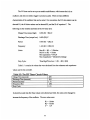
1
A CONTROL SYSTEM FOR A TESTHEAD MANIPULATOR
RollandL. Doubleday, Jr.
Bachelor of Engineering Science, Systems and Control
Montana College of Mineral Science and Technology, 1994
Submitted to the Department of Mechanical Engineering in Partial Fulfillment of the
Requirements for the Degree of
Master of Science in Mechanical Engineering
at the
Massachusetts Institute of Technology
May 1995
©Massachusetts Institute of Technology 1995
All Rights Reserved
Signature of Authc
'~ - ZIepartment of MechanicalEngineering
May 12, 1995
Certified
by
Alexander H. Slocum
Engineering
of
Mechanical
Associate Professor
Thesis Supervisor
Accepted by
..........
;:sAAC,-HUSETTS
lNosTrt-UTE Chairman, Department
OF TECHNOLOGY
AUG 31 1995
LIBRARIES
fark-- ,
Pi0ofesor Ain A. Sonin
Graduate Committee
A CONTROL SYSTEM FOR A TESTHEAD MANIPULATOR
by
Rolland L. Doubleday, Jr.
Submittedto the Department of Mechanical Engineering
on May 12, 1995 in partial filfillment of the
requirements for the Degree of Master of Science in
Mechanical Engineering
Abstract:
A mechanical manipulator was produced to position the many testheads used by
Teradyne. A control system was developed to meet specifications set by this group as well as
the specifications dictated by the mechanical design. This is a narration of the design process,
the roadblocks and retreats, as well as the occasional "no strings attached" success.
Three different levels of control were investigated to see if they satisfied the system
requirements. The first consisted of microprocessor circuitry that could be used with classical
control algorithms. The next level was a few steps down and used simple pushbutton logic
from a pendent to control the five motorized axes of the manipulator. The third was the use of
EPROMs as motor state selectors and simply worked as a lookup table to match combinations
of TTL inputs to desired TTL outputs that were signal conditioned to run the various relays
and brakes. All three levels of control were checked for performance, with documentation
presented of the reasoning behind each design.
Thesis Supervisor:
Title:
Dr. Alexander H. Slocum
Associate Professor of Mechanical Engineering
2
ACKNOWLEDGMENTS
This will not be the normal acknowledgments section [10] in which everybody will be
mentioned, including the family dog and pet goldfish. Somewhere along the line, I made the
mental decision to become an Engineer, and this decision came from somewhere. I have
always had a fascination for the finesse that can be found in the control of mechanical systems,
and bringing modem day control theory coupled with the appropriate voltage and current to
attack a problem. There are many people who have directed my flow in this field.
I would like to thank my Dad for always saying the right thing to keep me going and
showing me that hard work and self discipline should be the norm and not the exception.
Thank you for passing on to me the cowboy mentality, and making me realize from time to
time that I am still just a college boy. The genuine love for controls that you shared with me
cannot be forgotten.
I would like to thank Neil Wahl, my instructor and advisor back at Montana Tech. He
would work continually if his students would just keep up to his pace, and didn't mind patiently
answering endless control questions or diving into a troubleshooting nightmare for hours on
end.
Alex Slocum has always attacked problems with total energy, and inspires the people
around him to do the same. He definitely leads by example, and probably has not slept a whole
lot this year. Hopefully the reward of tenure will be his at the end of this project, and if not, he
can "sic" me on them. Thanks, also, for making MIT so affordable; it's really nice not to be in
debt at the end of this degree.
Joe Kujawa has been a friend that has provided support in the past as well as help with
this project. His troubleshooting skills are finer than mine, as have been proved and put to use
many times in the past.
Dirk Danninger has always made himself available in the past for controls questions,
and a lot of what I know about the 8052 microprocessor came directly from him.
I would like to thank Conrad Hilpert for instilling in me a little cynicism towards
academia. His worry that I would be attending a non-accredited university when leaving for
MIT was really touching, as well as the call he made to MIT admissions discussing his worries.
Dr. Hilpert can always see the humor in a situation, as well as reminding me that I am still a
college boy.
Baily Hinds has hired me several times to work in the Kuparuk Oil Field of Alaska.
This has given me a chance to work a set of tools, see the world from the eyes of a rigger and
technician.
3
Thanks also to R.P. and Frank, the heads of the Teradyne electrical section of this
project. They have been truly helpful on this project, no matter what I might say under my
breath from time to time, and have provided a very valuable consultation resource.
Thank God for providing 24 hours in a day.
4
Love to the woman who knows me as S.S.B.
5s
TABLE OF CONTENTS
Title Page .......................................................
Abstract...............................................................................................................................
A cknow ledgm ents ..............................................................................................................
Table of Contents ....................................................................................................
List of Figures ........................................................
1
2
3
6
8.....................................
List of Tables ........................................................
10
Chapter 1: Introduction........................................................
11
Chapter 2: The System Hardware .......................................................
16
2.1 The Joystick .......................
.................................
2.2 The Pendant .......................................................
2.3 Evolution of the Twist Axis ........................................................
2.4 Evolution of the Up/Down Axis.......................................................
2.5 Evolution of the In/Out and Theta Axes ........................................................
2.6 Evolution of the Side/Side Axis .......................................................
2.7 Cost Breakdown ........................................................
2.8 Some Early Design Switching Issues........................................................
2.9 Limit Switches ........................................................
2.10 Pressure Switch ......................
..................................
2.11 Swing Brake Solenoid ........................................................
Chapter 3: The Microprocessor Design ........................................................
3.1 Microprocessor and Microprocessor Support Chips.
..................................
16
18
22
30
32
36
38
39
41
41
42
43
46
3.2 Memory (RAM and ROM .......................................................
52
3.3 The Display and Display Support Chips.......................................................
3.4 The Signal Conditioning to the Counter Pins on the Microprocessor ......................
3.5 The A/D Converters Used To Bring the Joystick Signals Into the Program ............
3.6 The D/A Converters and the Output Signal Conditioning.
...........................
3.7 The 8255 PIAs Used For I/O to the D/A's and From the A/D's, Respectively .......
3.8 Design Considerations For Microprocessor Board Improvement ............................
3.9 Troubleshooting the PCB Board Design .......................................................
3.10 Quadrature Decoding ........................................................
57
63
64
67
70
72
78
85
Chapter 4: The Pushbutton Logic .......................................................
4.1
4.2
4.3
4.4
88
The High/Low Speed Circuitry .............................................................................
88
The Logic to Run the Up/Down and Twist Axes .
....................................................
90
The Logic to Run the In/Out, Theta, and Side to Side Axes .................................... 92
The Addition of Limit Switches .......................................................
94
6
Chapter 5: Control Through EPROMs .....................................................
99
5.1 Circuitry ...................................................................................................................
5.2 Memory Mapping .....................................................
5.3 Definition of EPROM Input and Output Variables ..................................................
5.4 The Boolean Expressions Relating Inputs to Outputs for the EPROMs ..................
Chapter 6: Improvements .....................................................
99
101
104
108
112
6.1 Replacement of the UDC-800 DC Motor Control Cards ......................................... 112
6.2 Stepper Motor Brakes to Electric Clutches................................... ........................... 115
6.3 Compliance Brake Logic ..............................................
....... ........................... 116
Chapter 7: Conclusions and Recommendations ........................................
References .......................................
..
............. 117
......................................................
...... ............ 119
Appendix A: The EPROM Truth Tables (In Binary) ....................................................122
Appendix B: The Truth Tables in Hexadecimal ........................................
............. 128
Appendix C: A Parts Listing for the Microprocessor Design ........................................135
7
LIST OF FIGURES
Figure 2.1 The Joystick Designed to Operate the Five Manipulator Axes ................... 16
Figure 2.2 An Early Pendant Design by Paul d'Entremont ........................................... 19
Figure 2.21 A Later Pendant Design by Frank Parrish ..................................................20
Figure 2.3 The Bodine UDC-800 DC Motor Control Card ....................................
24
Figure 2.31 The UDC-800 Speed Control Terminals......................................................25
Figure 2.32 The UDC-800 Card Disable Terminals........................................................26
Figure 2.5 An Early Block Diagram of the System Switching ....................................... 33
Figure 3.0 Schematic of the Controller for the Teradyne Magnum Manipulator ....... 45
Figure 3.1 The Reset Circuitry .........................................................
50
Figure 3.2 The Allocation of Memory in the p.PCircuit Design .................................... 54
Figure 3.21 The LS74138 Decoder .........................................................
54
Figure 3.22 More Efficient Use of the 74138 .........................................................
55
Figure 3.23 A Block Diagram of the PCB Board Designed.
56
...............................
Figure 3.3 The 4x20 LCD Display Address Map ......................................................... 58
Figure 3.4 A Block Diagram of the System with Hall Effect Sensors ............................ 63
Figure 3.5 The 555 Timer Used For a Clock Signal to the A/D's ................................... 64
Figure 3.51 The Wiring of the AD0804 Analog to Digital Converter ............................ 66
Figure 3.6 The DA0808 Digital to Analog Converter .....................................................68
Figure 3.61 The Output Signal Conditioning .........................................................
68
Figure 3.7 The 8255 Control Word ........................................
70
.................
Figure 3.8 The Resolution of the Theta Axis ........................................ ...................... 72
Figure 3.9 The Silk Screen Layer of the PCB Board Designed................................... 75
Figure 3.91 The Component Layer of the PCB Board Designed ..................................76
Figure 3.92 The Solder Layer of the PCB Board Designed............................................77
Figure 3.10 TTL Equivalent of the Quadrature Decoding Program ............................. 86
Figure 4.1 The Circuitry for the High/Low Speed ..........................................................88
Figure 4.2 The Ladder Logic for the Vertical and Twist Axes...................................
90
Figure 4.21 The On/Off and Directional Switching...................................................... 91
8
Figure 4.3 The Ladder Logic for the In/Out, Theta, and Side/Side Axes ..................... 92
Figure 4.4 Limit Switch Logic for the Up/Down and Twist Axes.................................. 94
Figure 4.41 Limit Switch Logic for the Side to Side Axis....................................
95
Figure 4.42 Expected Limit Switch Mounting on the In/Out and Theta Axes............. 96
Figure 4.43 The Limit Switch Logic for the In/Out and Theta Axes ............................ 97
Figure 5.4 The EPROM Circuitry and Supporting Chips...................................
100
Figure 5.41 The TTL Equivalent of EPROM 1......................................................
109
Figure 5.42 The TTL Equivalent of EPROM 2.....................................................
110
Figure 5.43 The TTL Equivalent of EPROM 3......................................................
111
Figure 6.1 Supplemental Wiring For the RG 300 UA Motor Control Card .............. 115
9
LIST OF TABLES
Table 2.3 Sense Resistor Values for Non-Bodine Motors ...............................................23
Table 2.7 A Breakdown of the Motor Costs for this System ..........................................38
Table 2.71 A Breakdown of the Motor Driver Costs for this System............................ 38
Table 3.2 The Controller Components and Their Place in Memory ............................. 53
Table 3.3 A Sample LCD Display Program ......................................................
59
Table 3.31 A Program to Use the Display and RAM Efficiently ................................... 61
Table 3.5 The 555 Timer Circuit Values ..........................................................................
65
Table 3.51 The New 555 Timer Circuit Values ......................................................
66
Table 3.9 Program to Check 8255's As Output Devices.................................................80
Table 3.91 Program to Check 8255's As Input Devices..................................................80
Table 3.92 Program to Check Optrex LCD Display ...................................................... 82
Table 3.93 Program to Automatically Range the Potentiometers ................................. 84
Table 3.10 Quadrature Decoding Program .....................................................................87
Table 5.2 A Listing of Inputs and Their Corresponding EPROM Addresses .............. 101
10
Chapter 1: Introduction
Teradyne is a billion dollar company that makes their money in the business of
electronics. Currently, they use a counterweighted mechanism to move their highly expensive
and heavy testheads to the docking area where wafers are tested. This docking area can be at
any variety of angles and orientations. This counterweighted version is/was old technology,
and Alex d'Arbeloff as the insightful engineer entrepreneur that he is, looked around for a
better solution. In the end, this problem was presented to the Precision Engineering Research
Group at MIT under Alex Slocum.
Alex was to recruit a team of graduate students that would come up with a design that
would match or beat the performance of the current manipulator design, while at the same time
matching or beating the price of the current system. Alex and these graduate students were
given roughly one year to come up with the design as well as two working prototypes. Since I
had a background in controls and electronics, the control system for this manipulator was to be
my responsibility.
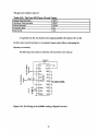
A mechanical manipulator with seven degree of freedom movement was developed
with two versions of control systems: the first and simpler version was to provide power to the
twist and up/down axis; the second would give a system with five motorized axis. The second
system would still have motors on the twist and up/down axis, but would add motorization to
the manipulator to give side/side movement, in/out movement, and theta movement. The theta
movement was provided for by synchronous and opposite rotation of two motors/actuators on
the cradle arms of the manipulator, and the linear, in/out movement was accomplished through
the synchronous operation and same direction rotation of the same two cradle actuators. The
11
side/side movement was provide for by an actuator/motor
located in the base of the
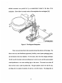
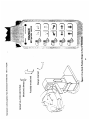
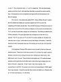
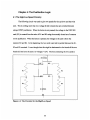
manipulator. Shown below is an early version of the manipulator that was designed [18].
Li
Figure 1.1 The Magnum Manipulator
There were some basic factors that constantly dictated the direction of this design. The
factors were cost, user friendliness (ergonomics), flexibility, control system packaging (space),
and development time (June deadline). For this reason, there were three designs developed.
The first was for the simple version providing power to only two axis, and this used a pendent
control/pushbuttons to run some switching logic to the motors. The second was a take off
from the first in that it used the pendent idea. This gave pendent control over the five axis,
providing only two speeds of operation, hi and low, to the five motors. This design did not
12
allow for the 55 degree coordinated movement. The attraction of this design was the short
development time and simplicity with regards to passing TUV inspection.
The third design was the most complex and flashy design (proposed by PERG student,
David Levy). This provided a joystick that resembled the actual testhead manipulator. The
joystick potentiometer signals would be taken to a microprocessor based controller that was
designed specifically for this control application. Being a potentiometer, it was possible to
provide variable motor speed. Coordinated motion could be provided for any angle of motion,
included the desired 55 degree specification. An LCD display would provide the user with
instructions and warnings about the use of the manipulator. Alarms would be sounded for
warnings to the user about misuse of the manipulator. In addition to these features, it would be
possible to program the EPROM through an RS 232 port, which would allow ease in updating
the control algorithm for the system. The drawbacks to this system was the development time
of the controller due to the bureaucracy present at Teradyne.
The evolution of this control system and the options considered is an interesting story
in that it shows that a cost driven design will not always have a lot of finesse. In the beginning,
there was talk of "automatic" docking, using proximity sensors and Delta Tau controllers to
accomplish the dock. This moved to open loop control to avoid having to play by the rules
that a fully robotic system would dictate, such as roping off the area and providing flashing
lights and bells to warn the workers of the docking process. A lot of thought was given to
produce a nice, ergonomic design for the above mentioned joystick that would "map" the
movement of the joystick to the actual movement of the testhead. Also, an effort was made to
13
anticipate all of the problems that might be encountered in this area by the user, and an attempt
to eliminate these problems was made through the ergonomics of the joystick.
Early on, without the controller specified, a microprocessor based controller was
designed and breadboarded. It seemed to have the capability of satisfying the design criteria
while maintaining a fairly reasonable manufacturing cost. This was then blocked since it looked
as though it would take too long for it to be certified for use in a clean room where people are
in close proximity to the robot, so an even simpler solution had to be found.
The next stage in the evolution of this system design was an extreme reaction to the
blockage of the microprocessor idea. It was an attitude of basic rejection to any electronics
solution that would require pcb boards, chips, etc., that might draw a large "time sink" in it's
commissioning. It was thought that if this problem could be solved through straight switching
and pushbutton logic, then this would be the solution that would most likely meet Teradyne's
approval.
This approach did not last a long time, though, when it was seen what would have to
be given up in terms of manipulator functionality to obtain this easy solution. In fact, the easy
solution was actually quite complex when researched, requiring sixteen, 4PDT pushbuttons.
Even with these special pushbuttons, functionality was sacrificed since there were not enough
poles in these pushbuttons to deal with new and improved logic requirements that had the
inclusion of limit switches.
The next stage was a "stepping back" from extreme design, and was the use of
EPROMs to be used as state selectors for the system. Truth tables were drawn up, some with
up to 12 columns and 100 rows, to give the desired motor response at any given combination
14
of pushbutton and limit switch state.
It required three EPROMs and various circuitry to
protect the EPROMs, as well as some relay drivers to accomplish the control goal.
*
Chapter 2 will introduce the hardware of the system, such as motors, amplifiers, relays,
limit switches, and basic motor controllers. The signal requirements of each will be
discussed, as well as the cost found for each in per unit and quantity measurements.
·
Chapter 3 will discuss the microprocessor circuitry that was designed specifically for
the manipulator control. The wiring of the circuit as well as the programming involved
in this type of control will be investigated. The focus will be on the capabilities of this
type of control.
*
Chapter 4 will layout the pendent pushbutton logic that was attempted for manipulator
control.
*
Chapter 5 will talk about the EPROM logic used for the manipulator control. The
basic wiring will be discussed, as well as the TTL equivalents of the information burned
into the EPROMs for comparison.
*
Chapter 6 will discuss the improvements that were made after the EPROM logic was
instilled.
*
Chapter 7 will examine the whole project and present conclusions and
recommendations for fiuturecontrol improvement.
15
Chapter 2: The System Hardware
2.1 The Joystick
The following is an illustration of the joystick that was developed to provide one
solution to the control of the manipulator system. The focus of the design was to provide a
"replication" of the actual testhead, which would make it easy to match joystick movement to
the movement of the testhead.
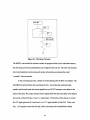
David Levy, a student in PERG, was the individual that
provided most of the ergonomic advice, and this design is a result of his ideas.
MSI Model510
SpringReturnPot
Affl-M-ft
Figure 2.1: The Joystick Designed to Operate the Five Manipulator Axes
The joystick was made to look like a testhead so that it would be possible to turn the
joystick in the orientation of the testhead to easily map the joystick movement to testhead
movement. The top of the joystick has an MSI model 510 spring return potentiometer. This
potentiometer is mounted with a 5/8-24 threaded bushing. This was used to give the theta
16
movement of the testhead. The potentiometer was 5 kf and gave 45 degrees of deflection,
and when +5V and ground were applied to this potentiometer, a voltage signal indicative of the
theta demand resulted. For zero theta actuation, a signal of roughly 2.5 V was produced. This
potentiometer was $83 for one unit, $44 in quantity.
To provide up/down, side to side, and twist motion, an MSI model 521Z three axis
joystick was utilized. It gave and x-motion that corresponded to the side to side motion, a y
direction motion corresponding to the up/down motion, and the end of the joystick had a
potentiometer that was a converted model 510 to give the twist motion signal. The 55 degree
docking requirement was taken care of in software by analyzing the up/down and side to side
voltages, and proportioning the motor speed with this information. Each was a potentiometer
that had +5 V and ground applied to it to produce a 0-5V voltage signal to represent each axis
motion demand. This potentiometer was $188 for one and $93 in quantity.
A three position slide switch was used to give the linear in and out motion of the
testhead.
In the prototype, an inexpensive, Radio Shack version was used, but it would be
desirable to replace this with a more robust, spring return potentiometer that could be used to
give variable speed as opposed to the on/off control provided by the slide switch.
The safety trigger is from Electric Switches Incorporated (cat. no. U2-016, military no.
M8805/111-001, otto P/N U2-016). It is .641" thick, 1.234" long, and .688" wide. The total
travel is .440". The safety trigger was included so that the motors would not actuate unless
this trigger was depressed. This safety trigger is the ergonomic equivalent of the pendant's
enable pushbutton.
17
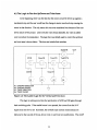
2.2 The Pendant
For some reason, there was a push for a pendent design to run the manipulator. On the
MIT side in the beginning, this idea was not taken too seriously in that it was a totally unergonomic approach to the problem. However, there was some pressure exerted from a few
different directions, and this idea was soon investigated. The first pendant proposal was made
by Paul d'Entremont [17]and can be found on the following page. It is the most simple of the
designs investigated, having two buttons to control each axis and then two enable buttons that
would require two handed control.
With new control requirements, buttons were added to give compliance to the in/out
and theta axis, the side to side axis, and the up/down axis. A pushbutton was include to release
the swing brake, and a high speed button was added to give two speeds for the up/down and
twist motors. This feature allowed high speed motor actuation when the testhead was a long
distance from the dock, and a "creep" speed for fine tuning the testhead position when
approaching the dock.
Also, a latch release button was added to block control from the
pendent and turn it over to Mike Chiu's linear planearization setup in a simple "hand shaking"
process. It should be noted that the ergonomics of this pendent design would require of the
user an Airline Transport pilot rating, a Commercial Driver's License, and have served as a
Navy fighter pilot to have the coordination to use it correctly. Being a private pilot myself, a
simple pilot's license does not seem to be enough training to run this pendent. On the page
following the first pendent design, a second design for the pendent can be seen. This was a
creation of Frank Parrish [8]. It should be noted that the pendant's used SPST momentary
pushbuttons for all of the inputs except for the high speed pushbutton and the toggle
18
C)*
0%4
-
~~~~~~~~~~~~
Lt)~~~~~~~~~~~~~~~~~~~~~~~~~~~~~~~~~~~~~~~~~~~~~~~~~~~~~~~~~~~~.
szC~~~~~~~~
C
10,
I.
e
Ln
Q~
9L.~~~~~~~~~~~~~~
IC
=.
,r
LU
>. '*
z
<A
LU
H-
a
C/)
N
0
_
E
E
3
E
:6n-
o
0
o
3
v1
CI
L-
z
CZ
E
i
,-
.0.
N
C4
vl
In
I.
co
PII
s.
em
;
PD
co
04
.u
vz
u
compliance switch. A DPDT pushbutton was used to switch between two combinations of
fixed resistors to produced a voltage divider signal to the input of the UDC 800 analog control
card. The toggle compliance input was in fact a toggle, on/off button.
Although not ergonomically optimal, the pendent could be inexpensive and produced
rapidly and reliably. This was the motivation to accept this solution for manipulator control.
21
2.3 Evolutionof the Twist Axis
Depending on whether the manipulator was to be used on the east coast or west coast,
there was to be 190 degrees of twist travel. It was desired to get this full rotational stroke
within 30 seconds, so a rotational speed of 1 rpm was chosen as something to shoot for.
Taking this back through some gearing (planet gear), this corresponded to a motor speed of
about 5 rpm. The maximum torque load was to be 3400 lb-in at the planet gear, which
corresponds to a motor torque of 340 lb-in. These torque values were found from cable force
measurements performed in October.
From the above criteria, a Bodine gear motor was chosen (by Ryan Vallance). This
motor delivers 300 lb-in and 13 rpm at this torque. At no load, it will rotate at about 17 rpm.
However, this rotational speed is reduced when taken through a gear having a 10:1 ratio.
Initially, the model 856 controller was purchased from Bodine to run this motor. It
took a plus or minus 10OVsignal as an input and gave a proportional output speed.
The
problem with this controller was that it did not provide reversing to the motor. A +10OVsignal
gave the same speed and rotation direction as a -10 V signal. Also, the motor was seen to drift
about one half a rotation after the control input was taken away. After consulting with Bodine
engineers, it was decided that an optional "forward-brake reverse (FBR)" kit would have to be
included. The price of the model 856 was $347 ($224 in quantity), and the FBR kit was to be
an additional $105 ($71 in quantity). In addition to these problems, the controller was quite
large (4.55"x7.27"x3.50").
A better solution to all of these problems was found in the form of an analog card and
some relay logic. The UDC-800 was chosen, which takes a voltage signal generated from a
potentiometer that comes with the package and gives a speed proportional to the pot voltage.
22
It runs off of 115 VAC, and produces an output voltage than ranges between 0 and 90 VDC,
with the output current limited by the value of resistance chosen for the "Sense Resistor." The
table shown below is a reproduction of the table found in the "Instructions for Installation and
Operation" produced by Bodine. They show the Sense Resistance values for non-Bodine
motors. It should be noted that for the 90V Bodine Motor that was used, a 0.1 ohm resistor
was used, as specified by a Bodine representative.
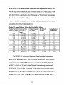
Table 2.3: Sense Resistor Values for Non-Bodine Motors
Typical Current
Input Current
Output Current
Dip Switch
Sense Resistor
Limit DC Amps
RMS (AC)
Amps
0.16-0.31
0.28-0.54
0.50-0.90
0.70-1.50
1.25-2.25
2.00-3.50
2.754.50
3.75-6.25
4.75-7.75
6.50-11.00
7.50-12.75
8.50-15.00
DC Amps
Settings
Value (ohms)
0.29
0.52
0.88
1.40
2.20
3.40
4.20
8.20
10.4
15.0
16.4
20.0
0.10-0.19
0.17-0.34
0.31-0.56
0.43-0.93
0.78-1.40
1.25-2.18
1.68-2.78
2.30-3.90
3.00-4.80
4.00-6.80
4.60-8.00
5.30-9.30
5
4
3,5
2,5
2,3,4,5
1,3
1,2,3,4,5
2,4,5
2,3,4,5
1
1,3,4
1,2,3,4,5
0.1
0.1
0.1
0.1
0.1
0.1
0.1
0.015
0.015
0.015
0.015
0.015
The UDC 800 DC motor control board was selected to run the Bison up/down
motor and the Bodine twist motor. This card converts a small current, analog voltage to
a high current, high voltage ranging from zero to 130 volts, but this output voltage can
actually be varied to suit the motor ratings. The speed is varied through three terminals:
S1, S2 and S3. S3 is +12 volts, S1 is ground, and the analog input is varied on terminal
S2. This variance at S2 can be accomplished through the use of a potentiometer used as a
voltage divider, or an isolated voltage signal, such as one from a D/A converter with op-
23
amp isolation. For the microprocessor board designed, this signal was generated through
an 8 bit D/A converter and the isolation was accomplished through an op-amp in the
differential configuration.
Lkw~~P
Pum
u's
mclm
~P
trpot
MAXdpe
*pmfe W
Pa e 1
-"WW ShA"_
1"
hnme_,
moor mlcrnemmd
nmmnm
pid
Page1_
Papr
CW
cw
RG
pomt
- m
b men
p 19
cw
MA
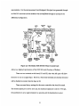
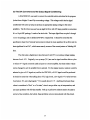
Figure 2.3: The Bodine UDC-800 DC Motor Control Card
Above is a digitized reproduction of the UDC 800 card (Courtesy of Bodine).
There are two terminals on this board, H1 and H2, that when left open will allow
the motor to run on a signal input. However, when these terminals are shorted, the motor
will be disabled no matter what the input at S2.
There are some factory settings for this motor controller that should be noted.
The minimal speed pot is set for zero rpm, the maximum speed pot is set for 1750 rpm,
the acceleration is set at approximately two seconds, and the deceleration is set at
24
approximately two seconds, also. The torque is set at 200% of rated load and is based on
the dipswitch settings. The settings are controlled through the minimum and maximum
speed potentiometers, the torque or current limiting potentiometer, the
deceleration/acceleration potentiometers and also the regulation potentiometer which all
can be found in Figure 2.3.
Modei 80a/803 Control Board
12V
10K
10K
MIN.SPEED
ADJUSTMENT
S2
FRONT VIEW
External Speed Potentiomete
10 K - CW rotation increases sp
Figure 2.31: The UDC-800 Speed Control Terminals
The analog input S2 and the ground on S1, as mentioned before, needs isolation.
The input should be conditioned to range between zero and ten volts DC. The motor
disable terminals, which are terminals H1 and H2, need to be optically isolated. If these
considerations are not taken, damage to the microprocessor board could occur.
25
Model 800/803 Control Board
I----------------------
.5 K
DISABLE
Close = Stop
Open - Run
Manual switch
or relay contacts
Figure 2.32: The UDC-800 Card Disable Terminals
To set the minimum speed , the minimumspeed potentiometer needs to be turned
fully counter clockwise, with this setting a starting point to adjust from. This minimum
speed adjustment will account for between 0-30% of rated speed, which means that fully
counter clockwise would correspond to 0 RPM, and fully clockwise would be 30% of the
rated speed. For the maximum speed adjustment, the maximum speed potentiometer,
when it is fully counter clockwise, will correspond to 60% of the rated speed, and will
correspond to 100% of rated speed when fully clockwise.
The torque adjustment can also be found on this card. Since torque is proportional
to current, this can also be seen as a current limiting adjustment. The torque trim
potentiometer has been set at the factory so that the motor will never see more than 200%
to 250% of its rated current input (according to Bodine). This adjustment should be set in
accordance with load requirements.
The acceleration adjustment can be made by turning the acceleration trim
potentiometer. Turning this counter clockwise will actually decrease the motor
26
acceleration time, with 0.2 seconds being the minimumtime to accelerate the motor to full
speed. The maximum acceleration time is 10 seconds, and can be achieved by turning this
pot clockwise. The deceleration adjustment is exactly the same as acceleration
adjustment, except that this is the time that it takes to go from full speed to 0 speed when
an input is taken away. These values also range between 0.2 seconds and 10 seconds,
respectively.
The most critical adjustment on this card is the regulation adjustment. This
regulation trim potentiometer is used to regulate speed under changing loads, and if you
have a constant load, it does not need to be changed. However, in our case, we are going
to have constantly changing loads and this has to be adjusted to account for it.
The steps for this adjustment are as follows:
(1) Determine the minimumand maximum positions of the trim potentiometer and
adjust them to 75% of the full clockwise rotation.
(2) Operate the motor at approximately 33% of the full speed and record the speed
at no load.
(3) Reconnect the load and operate the motor again, adjusting the pot until the
motor reaches the unloaded speed recorded in step 2.
(4) Disconnect the load and operate the motor without adjusting the speed control
and measure the unloaded speed. If it is the same as the value recorded in step
2, no further adjustments are required. The control is now calibrated
for minimum speed changes under varying load conditions.
(5) If, however, the unload speed has shifted, repeat the procedure until more
accurate regulation is achieved [2].
27
There were problems that were noticed with the alpha version of the manipulator
when it was powered the first time. The gears that connected the motor to the ball screw
were not meshing perfectly, which gave a changing load. This gave a varying voltage out
to the motor to try and compensate for the changing load (the torque changed, so the
voltage changed, also). After the regulation adjustment was made, these problems
disappeared, and the motor performed at a fairly constant speed through the full up/down
stroke of the Bison motor and the twist of the Bodine motor. These problems developed
on the day of the alpha electrical presentation to Teradyne representatives and was slightly
unsettling.
One troubling specification set by Bodine is the normal operating conditions,
which calls for a duty cycle of 8 hours per day, 5 days per week without frequent reversals
and starts or stops. This could prove to be a little inadequate, depending on how had the
manipulator shall be used.
The dimensions of the UDC 800 control board are 4.4 cm wide x 3.7 cm deep x
1.3 cm long and the net weight is one pound. The control speed range is up to 50/1 ratio
and this motor controller can handle up to a 3/4 horse motor. It requires 115 volts AC
and can run at 50 or 60 hertz, but if it is run at 50 hertz, the R41 resister needs to be cut.
There may be problems in the future confusing the board that will be used for twist motor
with the one used for the up down motion because the up/down motor (Bison) is limited
to 90 volts DC while the Bodine gear motor can be ran at 130 volts DC and actually needs
to be ran at this value to obtain the speed that we will require of it, which is 1 RPM of test
head twist. They both require different sense resistors. The Bodine requires a .01 ohm
sense resistor while the Bison requires a .015 ohm sense resistor.
28
In critiquing their
design, the logic that they use to disable the motor seems exactly backwards. They
actually short terminals Hi to H2 to disable it, which is not fail safe. If you remove the
wire from Hi to H2, the motor can run, and for this reason, we need to actually "hot
switch" the power from the UDC 800 with a relay. If this was not the way it was set up
and you had to short HI to H2 to run it, we could actually switch the AC power input to
it and go to a much smaller relay.
Limit switches were used to limit the motion of stroke to the 190 degrees of rotation
specified by Teradyne. Since this was a gearmotor and not back driveable, no brakes were
required to keep this motor from rotating during a loss of power.
29
2.4 Evolutionof the UP/Down Axis
There were many different ideas tried before the final selection was made for the
actuators, amplifiers, motors, and controller interfaces to be used in the final Teradyne
Magnum Manipulator. In the beginning, the up/down axis was to be run with a PMI motor.
Several of the motors from this distributor were checked for torque, speed range, packaging,
price, and other basic criteria, and were found to fall very short. The representative was also
fairly difficult to deal with, and was very reluctant to give pricing for two hundred fifty units a
year.
The next idea that was checked was using a Milwaukee drill motor to run the up/down
lead screw. The drill would have to be torn apart and some sort of mounting developed for it,
but the main drawback of this idea was the noise generated by the drill motor. It was rejected
for this very reason.
The last and final up/down axis driver tried was the Bison 300 VDC motor [12]. This
worked fairly well for the price, matched the torque and speed requirements of the system, so
this was chosen to run the up/down actuator.
The UDC-800 motor controller board was also used to run this motor. The only
difference between the two setups were the sense resistors used; the Bison called for a .01592
resistor. Also, the min and max speed would be varied by the manipulator assembler.
Two form CC relays [14] were used to switch the power from the UDC-800 card to
the motor, as well as reversing the polarity to give reverse motor direction. Dynamic braking
was accomplished by tying a 25
, 25 W resistor between the motor power lines when power
was removed from the motor.
30
An Inertial Dynamics brake was used on the Bison motor that would be engaged unless
24 VDC was applied to it. This was fail safe in that if there was a power failure, the up/down
axis would be locked. This brake required .369 A at 24 VDC. A mistake was made in the
beginning in that a 90 V brake was used, and the motor leads and brake leads were tied in
parallel. The problem with this setup was that the motor would only see 90V at the top speed
range, so the brake was always engaged unless operated at high speed. The "staying" voltage
required to keep the brake disengaged was much less than 90V, but this was irrelevant since it
was not desired to run the motor at full speed before running it at a lower speed.
Compliance in this axis was to be provided by a "cushion of air," first by an air piston
and finally by some Firestone Airstroke Cylinders. Compliance brakes were added to "lock
out" this compliance when not desired, such as when the manipulator was kinematically
coupled to the handler. Two, 24 VDC Warner brakes were used for this purpose, each
requiring .733 amps to disengage. As pointed out in a meeting, this compliance could be eaten
up by external influences, such as a cable bundle riding on the testhead, so limit switches were
added to alert the system of this occurrence. Limit switches were also used to limit the stroke
of the up/down motion so that the Bison motor would not be run after reaching a mechanical
stop.
Due to a load that would drive the motor, turning the motor into a generator, the
Bodine UDC 800 card was replaced with a Minarik RG 300 UA Regenerative Control card.
This card could provide a reverse bias to slow the load as the testhead was lowered. This
removed the Potter and Brumfield relays from the design, replacing them with small SPDT,
solid state pc relays. This will be discussed more in the "Improvements" chapter of this thesis.
31
2.5 Evolution of the In/Out and Theta Axis (s)
At first, drill motors were investigated as a possible driver of these two axis. However,
due to the noise produced by these motors, this idea was quickly rejected.
Thompson actuators were then selected to run these two axis. Western servo
amplifiers were used to take a plus or minus 10 VDC control signal and convert it to a higher
voltage/current signal to run the Thompson motor/actuator combination. The problem found
with this idea is the need for position feedback on the Thompson actuator in the form of Hall
Effect Sensors. These produced a current sinking pulse which could be signal conditioned to
produce a TTL logic high every .033 inches. Another problem found was that the shaft of the
Thompson actuator would start to rotate at the end of the stroke.
Western Servo had two types of amplifiers that could be used. A "linear" amplifier
could be used, but was more expensive than the "pulse width modulation" amplifier they
supplied. The problem with this type of amplifier was that it had problems with high frequency
noise, which was evident the first time the actuators were run. The actuators would actually
vibrate from the constantly changing amplifier signal to the motor due to this noise.
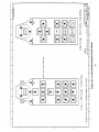
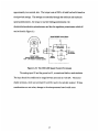
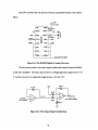
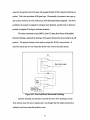
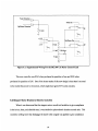
A simple diagram of this earlier system is shown below.
32
OF9off/
F.,-dl
OO11O
Fcn1
.80VDC
Fest
PMI
*32VDC
MOTOR
Fy~~~~~d1vn
.80VoC
*32VDC
WESTERN
DAC1O
af (*-IOV)
oES:ER
SERVO
AMP 1
RI
WESTERN7
'"l -gLEFT
---
CARRIAGE
MOTOR
RIGHT CARRIAGE
MOTOR
AMP2
Figure 2.5: An Early Block Diagram of the System Switching
To get more accurate theta movement, a stepper motor system was selected. A
stepper motor was to be placed in each carriage arm, and to get linear in/out movement, the
steppers would rotate in the same direction and speed. To get theta movement, they would be
run at the same speed but in opposite directions. This setup would give highly precise
movement that could keep the center of the testhead constant. The steppers at "half step"
settings would give .9 degrees of shaft rotation per stepper pulse.
The 23D204 stepper motor from Anaheim Automation was chosen for the carriage
motors. This is a four phase stepper, with options of full and half stepping. It boasts a "fast
damping" feature for better control, low noise, and high torque to package size ratio. The
specification sheet on this motor calls for 1.8 A/phase. The motor has a 1/4" shaft diameter,
33
and requires 100 oz-in. of holding torque. This is the torque that is required to make the motor
backdrive. Although backdriving in most motors can be seen as a form of compliance, in
stepper motors this is not true compliance, since there is no springiness to the motion, and once
the motor steps to a new rotation angle, it stays there.
The TM3000 trackmount driver [11] was selected as the amplifier to run this stepper
motor. This motor requires 12-28 VAC or 10-40 VDC for a power input. The inputs are
TTL and CMOS compatible. The excitation choices are dual phase, full step operation as well
as half step operation. The full step operation is brought on by energizing only two of the
phases at a time, while half step operation will be seen when all four phases are energized. The
half step mode seemed to provide better performance in that it was possible to run the motors
slower with less vibration.
Some of the most important inputs to this amplifier are the on/off, direction control,
clock, and mode select inputs. There is also a +5VDC output on the amplifier that could be
used to run some logic circuitry, but it is limited to 100 mA. For this amplifier, a logic "0" is
defined to be between 0 and .8V, and a logic "1" signal is defined as 3.5 V-5.0 VDC.
A logic 1 to the direction control bit (bit 3 of terminal block 2) makes the motor turn
clockwise, while a logic 0 makes the motor turn in a counter-clockwise direction. The motor is
on when a logic
is seen at bit 5 of terminal block 2. A logic 1 at bit 4 of TB2 gives half step
operation, while a logic 0 gives full step operation. The problem with this amplifier is that bit 5
of TB2, the on/off control bit, is pulled high with a 10 kQ resistor. This means that if the wire
running to this bit is severed, the motors run. This may cause problems with TUV inspections,
and Anaheim may be approached to place a pulldown resistor on this bit in their custom
engineered package for the later versions of the manipulator.
34
The speed of the motor was varied by changing the frequency of the oscillator signal
taken to the amplifier. The oscillator that was used was the AA2076 from Anaheim
Automation. This element was powered with 9-12 VAC. There were two speed ranges, low
and high, giving a square wave signal that varied 40 Hz-2kHz and 450 Hz-24 kHz,
respectively.
The run input on the oscillator was a logic "0", and the stop input was a logic "1."
Since this bit had a 4.7 kfl pullup resistor, this was a good setup; if the wire came loose, the bit
would be pulled high, turning the oscillator off.
The amplifier's 12-28VAC power supply requirement and the oscillator's 9-12 VAC
power requirement was taken care of with a 200W transformer with three taps on it; between
the middle tap and either of the other two taps was a voltage of 12.6 VAC, and between the
outer two taps, a voltage of 25.2 VAC was produced. This transformer was also purchased
from Anaheim Automation.
Compliance in this axis was to be given by disengaging the Lenze stepper brakes and
just "back driving" the stepper motors. However, when the alpha was up and running, it was
seen that no brakes were needed in that it was impossible to back drive the stepper motors.
This provided a control problem since it was impossible to provide compliance in this axis with
this setup. For this reason, the stepper brakes were discarded, a single ended stepper motor
instead of a double ended stepper motor was selected, and an electric clutch was used to
provide compliance. The clutch was to be engaged always unless a manual compliance button
on the pendent was pressed, in which the clutch would disengage and compliance in these axis
would be present.
35
2.6 Evolution of the Side/Side Axis
The same ideas tried on the In/Out and Theta axis were tried on this axis. Stepper
motors were also selected to drive this axis, and the compliance issue was treated in the same
manner.
A schematic of this total system can be seen on the following page.
This includes
information on the hookup of the Anaheim stepper motors and amplifiers and the UDC 800
Motor controller cards.
36
0u
r
C
(
c
a
c
,I I & -IU I ',
&.
1 , 1
6
.,V
*E
1
N-e
j
I
'.a
2
cm."
I
I
.
c" D
>
E
O
a
U
a
1 11I .
U< O
0I.
C
0
o
Q
C
4
ID
OO
nI
cc
_
__
I
4
a~a
W
_mt
zo -
maz
+-um
c ZE0J
IUzo
o
o
"I-
3
_h -h
P,
>a §m
Z
Jo
wurn
JH
noi
113
I
H
z i-0na
IF
I
Iz
ULLZH L
JCZIZJLU
i\I- z0wa
et
c
1
<CCCzf-i
vC
Jc
%P
D
oz
>-ZO
wum
Q.
OCI
-
J -
a,
2.7 Cost Breakdown
Table 2.7: A Breakdown of the Motor Costs for this System
Axis
Motor
Manu.
Twist
Bodine
Model # or
Descriptio
Voltage
(VDC)
Current
(A)
Cost per
one ($)
Cost per
250 ($)
90V
1.8 A
378.45
277.06
90V
2.76 A
250
10-40V
2A/phase
nominal
2A/phase
581/3
513/3
581/3
513/3
581/3
513/3
Misc.
Costs ($)
n
42A-GB
PM DC
Up/Down
Bison
Side/Side
Anaheim
Left
Anaheim
Carriage
Right
Gearmotor
(300 lb-in)
300 DC,
1/4 hp, 106
in-lb
TBD3XXX
X
TBD3XXX
10-40V
X
Anaheim
Carriage
nominal
TBD3XXX
10-40V
2A/phase
X
nominal
Table 2.71: A Breakdown of the Motor Driver Costs for this System
Axis
Model #
Cost per one ($)
Cost per 250 ($)
Twist
Driver
Manu.
Bodine
UDC-800
80
60
Up/Down
Bodine
UDC-800
80
60
Side/Side
Anaheim
Included above
Included above
Included above
Included above
Left Carriage
Right Carriage
Anaheim
Anaheim
Included above
Included above
Included above
Included above
Included above
Included above
Included above
Included above
Misc. Costs ($)
It should be noted that there is a one time engineering fee of $4500 for designing the
simpler system to run the stepper motors.
38
2.8 Some Early Design Switching Issues:
The following were the control options for the Teradyne Magnum Manipulator
when Western Servo amplifierswere to be used:
1.
Two Western Servo amplifiers with a 2 amp chassis/power supply.
2.
Two Western Servo amplifiers with a 2 amp chassis/power supply and a Bodine
amplifier/power supply/analog interface/forward brake reverse (FBR).
3.
Four Western Servo amplifiers with a 4 amp chassis and a Bodine amplifier/power
supply/analog interface/forward brake reverse (FBR).
4.
Five Western Servo amplifiers with a 6 amp chassis/power supply.
Choice 1:
If two Western Servo amplifierswere used to control the 5 motors, then there
would be a need to use relays to switch the amplifier's output to the motors, depending on
the joystick state. This would limit the movement of the manipulator to only 2 axis
movement at any given time. This would work, since only the linear in and out motors on
the carriage and the up/down and side/side motors (for the 55 degree dock) need to be run
at the same time. In software, the movements could be given a precedence by having
whichever joystick demand came in first to be the one that is acknowledged.
However,
this is only a possibility if we can replace the 90V Bodine motor used for the twist axis
with a 36 V equivalent. Position feedback could be obtained for all five axis's with only
the two internal 8052 counters.
39
Choice 2
This is the same option as choice one, except that the 90V Bodine motor is not
replaced with a 36 V motor.
Choice 3
This option has four amplifiers from Western Servo (and it's accompanying 4 axis
chassis/power supply) and the 90 V Bodine motor amplifier and power supply. This
option uses no relays to switch between the controlled axis, so it does not have the
limitation of only 2 or 3 axis control. Since no relays are used, no I/O lines are needed
from the controller. There is still only position feedback on two axis's, which will now be
dedicated to the in and out motors, since there could be the possibility of them binding up.
This eliminates the worry that the software will switch one relay closed before opening the
previous closed one, and having two different signals "fight each other."
Choice 4
This is the same as choice 3, except that the Bodine motor is eliminated for a 36
volt equivalent, and a 6 axis chassis power supply will now be used.
These were some of the factors in the decision making process. It was not
desirable to have any switching, but since the design was very cost driven, it was
necessary. In the end, it was decided to switch between two Western Servo amplifiers
running three Thompson actuators, and have separate cards to run the Bison and Bodine
motors. However, these complicated issues disappeared when the decision was made to
go to stepper motors for side/side movement and in/out and theta movement.
40
There was some talk of using one UDC 800 card, and switching the output to the
Bison and Bodine motors, but since the card was so inexpensive, it was decided to have
one for each motor.
The biggest consideration when deciding to use any relays for switching was the
presence of the TUV influence. Each additional element in the electrical design would be
one more element for TUV to molecularly disassemble. For this reason, the design that
produced the least amount of switching was the most desirable.
2.9 Limit Switches
Twelve limit switches were used in the system to give limitations to the stroke of
the up/down, twist, in/out, theta, and side/side motions as well as an up/down compliance.
The V3-101-D8 miniature limit switch from Micro Switch was selected to serve this
purpose. The normally closed contacts on these limit switches were used so if the lines to
the limit switch were broken, it would give an indication of a "made" switch. This made
them more fail safe for TUV.
2.10 Pressure Switch
The PSW-523 [13] pressure switch from Omega was selected to give an indication
of the pressure in the air cylinder. This pressure switch could be mounted in systems
seeing up to 100 psi, and the pressure at which this device switched could be varied
between 3.0 psi and 96.5 psi. The deadband for this unit is 1.5 psi to 3.5 psi, depending
on the switching pressure. The normally closed contacts off of this unit were also used for
the same reason mentioned in the limit switch section. Logic was provided to disallow
41
up/down movement and engage the up/down brake if the air cylinder pressure was not
present in the system, which was indicated by this pressure switch.
2.11 Swing Brake Solenoid
This solenoid had quite a history in the development. In the beginning, a solenoid
was selected that required upward of 80V for a few millisecondsto get the solenoid to
disengage the swing brake, and about 28V to maintain the disengagement. Some thought
was given to amplifier logic that could accomplish this, as well as switching power to it
with relays. One design was developed that would actually apply 90 V to the solenoid,
and when the rod of the solenoid was pulled back in the solenoid case, a lever would
actuate throwing a resistor in series with the solenoid. This gave a resistor/solenoid
combination that acted as a voltage divider, and the appropriate resistor size could be
selected to give a voltage drop of 28 V across the solenoid.
These considerations were made so that a smaller solenoid could be used and it
would be easier for the mechanical designers to package it. However, this design was
complicated and required a 9OVDC power supply to run it, and since it was an expensive
electrical solution to a mechanical packaging problem, was quickly discarded.
The Warner ERS 49 brake was selected for this axis. It is a failsafe brake that
requires voltage to disengage. It is rated at 24 VDC and 1.136 A.
42
Chapter 3: The Microprocessor Design
There are many components to the basic 8052 circuit [1,3] that was developed to
control the magnum manipulator for Teradyne. They can be broken into several categories,
such as:
I.
The Intel 8052AH Microprocessor (with onboard compiler) and microprocessor
support chips
a.
Port 1
b.
The Data lines, Address lines, and the 74573 Tri-State Octal D-type
Latch (Address Latch)
c.
The internal counters (TO and T 1)
d.
Reset
e.
Serial input and output and the Max 232 serial interface chip (Only
included in the prototype version)
II.
mI.
f.
Read and write
g.
XTAL1 and XTAL 2 and the 11.0592 Mhz clock
h.
The interrupt lines
i.
Pulse width modulation
Memory
a.
8Kx8K Static RAM
b.
74138 Decoder (one of eight) and memory mapping
c.
27128 EPROM
d.
EPROM programmer (only included in the prototype version)
The display and display support chips
a.
Optrex 4x20 LCD display
b.
7400 NAND Gate chip
43
IV.
The signal conditioning to the counter pins on the microprocessor
V.
The A/D converters used to bring the joystick signals into the Basic 52 program
VI.
a.
The reference voltage signal
b.
The clock signal (555 timer)
The D/A converters and the output signal conditioning used to take the controller
action to the motor amplifiers.
a.
VII.
The reference voltage signal
The 8255 PIA's that were used to send out and bring in the information to the D/A's
and from the A/D's, respectively.
All of the above information can be found in this chapter. Hopefully, by listing it in a
logical order, the understanding of the topics discussed will come easier.
44
CL
C
et
E
5=
'0
(-
6
to
._
o
.)
CO.-
-eEE
s~~~: ;Bes|E
I
i
err1
1
3.1 Microprocessorand MicroprocessorSupport Chips:
With the control of the manipulator still up in the air, microprocessor circuitry was
investigated that could accomplish this task. In particular, the Intel 8052 and supporting chips
was selected. This chip can be considered an "embedded controller" in that it acts as a mini
computer and can be reprogrammed to suit the control need. This option has several
advantages over using a pc or some commercially available controller to run the manipulator.
These include lower cost, smaller packaging, less power consumption and stand alone
capabilities. The main drawback to this option is that it intimidates the marketing personnel
trying to sell this to the public.
Embedded control [4] will usually fall into one of three categories: Sequential control,
closed loop control, and data control. Sequential control can be found in most machine tooling
processes. An example of this would be a high speed drilling operation in which parts on a
conveyor belt are brought to a drill until a limit is made that indicates proper positioning. The
conveyor is turned off and the drill is turned on. Next, the drill is lowered to a certain depth
over a given amount of time to drill the part. Finally, the drill is retracted, the limit is reset, and
the conveyor is restarted.
Data control would be for the application of state control in which a lot of I/O work is
needed. An example of this would be the monitoring of limit switches and pushbutton states,
and then making decisions on the desired output (sound familiar).
Closed loop control would involve classical control techniques such as P+I+D control.
A process variable would be monitored, and depending on the setpoint, a calculated corrective
action would be sent out to a final control element to change the process variable and bring the
46
error to zero. The control algorithm would be digital in nature with the resolution depending
on the number of bits that are used to bring in the information to the controller.
There are several microprocessors in the Intel family similar to the one that was used
for this design. The 8052AH with onboard Basic was used, but several could have taken it's
place. The 8051, for example, has:
*
*
*
*
*
*
*
*
*
*
*
8-bit CPU optimized for control applications
Extensive Boolean processing (single bit logic) capabilities
32 bi-directional and individually addressable I/O lines
128 bytes of on-chip Data RAM
Two 16 bit timers/counters
Full duplex UART
5 source interrupt structure with two priority levels
On chip clock oscillator
4K bytes of on-chip Program Memory
64 K Program memory address space
64 K Data memory address space
The 8052 AH Basic has the additional improvements over the 8051:
*
*
*
*
256 bytes of on-chip Data RAM
Three 16 bit timers/counters
6 source interrupt structure
8K bytes of on-chip Program Memory
Microprocessors have sometimes had a bad reputation follow them around, and this
could be due partly to a lack of understanding. The following sections will go through and try
to increase the readers understanding of the circuitry used to control the manipulator as well as
the programming capabilities. Hopefully, this may dispel some of the worries that marketing
had about the use of a microprocessor to control the manipulator.
Port 1 on the 8052 are the first eight pins on the 8052AH (P1.0-P1.7). Some of the
pins may be used as input/output bits, and were found through experimentation to be bits 0-2,
47
4, and 6-7. This corresponds to pins 1-3, 5, and 7-8, respectively. There are internal pullup
resistors on the bits of port which make them float high, so a ground true must be used for
input. Bit manipulation can be accomplished with logical AND and OR statements in the
Basic-52 language.
Pin 4 of port 1 is the address latch enable (NOT). This is ANDed with pin 30, which is
the ALE (address latch enable) pin, to produce a signal to the 74573 to control the
multiplexing of the address and data lines. Since the 8052 only has an 8 bit data bus, but has 16
address lines, the lower 8 bits of the address are shipped out on the data bus and latched by the
74573, and then the actual data is shipped out on the data lines. This latching is enabled by this
ANDed combination. The upper eight address bits are shipped out on lines A8-A15, as
expected. The 573 was used over 373, since the 573 provides a straight shot through to the
other side, input to output, which makes the circuit board design a little simpler. It should be
noted that the 8052 automatically takes care of this latching and was not part of the controller
program.
In the beginning, Thompson PPA actuators were to be used for the in/out, theta, and
side/side motions. These motors could vary as much as 15 %, so there was a need for position
feedback to keep the motors turning at the same rate to maintain pure, linear motion. Hall
effect sensors were to be used. These produced a pulse signal every 0.033 inches of actuator
extension, and this pulse from the hall effect sensor on the left and right carriage motors was
taken to TO and T1, respectively. TO and T1 (pins 14 and 15) are internal, 16 bit
counters/timers to the 8052. The counters were turned on by manipulating the TMOD register
with a logic statement. It should be noted that these counters can handle up to a frequency that
is 1/24 of the clock frequency (11.0592 MHz).
48
The terminals 12 and 13 are the interrupt bits of this microprocessor. These bits can be
connected to logic that will generate a low to interrupt the routine that is running in RAM.
The "ONEXO" and "ONEX 1" statements can be included at the beginning of each program to
give the microprocessor a set of instructions to follow upon an interrupt being sensed. Usually,
this statement can point to a subroutine that will only be encountered on the generation of an
interrupt.
These interrupts could be used to replace the pendant with a hex key pad. A hex key
pad is nothing more than what is found in most office telephones, and can be purchased
separately from a telephone. This pad has sixteen keys, and the 74922 chip can be used to
interface this module. Only four address lines and a chip select line are required. The interrupt
line senses when a key is pressed, and the external byte statement can be used to pull off the
lower four bits of the data which correspond to a specific key hit. Then, a specific subroutine
can be assigned to be run on a specific key hit.
A nice feature of using this over the pendant is that the hex key pad is extremely light
weight, not to mention that a template can be easily layed over the top of the keys if there is a
need to change the function of the keys or relative locations.
A momentary, normally open pushbutton was used, along with a 4.7 uF capacitor and
a 1 kfQ resistor, as a RESET to the 8052 (pin 9). When the button is pressed, the capacitor is
shorted and pin 9 sees a high. When it is not pressed, the capacitor charges, producing a low
to pin 9. This means that this is a RESET high situation.
49
3
Figure 3.1: The Reset Circuitry
The RESET was included for situations where the program locked up for unforeseen reasons;
the same thing could be accomplished by just turning the total unit off. This reset was included
only in the breadboard version since each jumper wire acted as an antenna that could
"crosstalk" with one another.
In the prototyping process, a means of communicating with the 8052 was needed. The
MAXIM 232 serial interface chip was chosen for this. It provides dual, serial port data
transfer, and the serial send and receive signals from an RS 232 connector were taken to the
inputs of this chip. The output send and receive signals from this chip were taken to the serial in
and out bits of the 8052 (pins 10 and 11, respectively). The function of this chip is to convert
the 12V signal generated by a serial port to a 0-5 V signal readable by the 8052. There were
four, .1 uF capacitors used with this chip, which went along with the specification sheets.
50
Other size capacitors were tried and worked, but a large deviation from this value caused
problems when downloading programs from the PC into RAM.
The clock that was used had a frequency of 11.0592 MHz. This signal was taken to
XTAL2 (pin 18) on the 8052, with XTAL1 (pin 19) taken to ground. This setup is not valid
for the "Micro-mint" version of the 8052.
A special bit that is contained within the port 1 bits is the PWM bit (P1.2, pin 3).
"Pulse Width Modulation" statements can be used to generate a square wave signal at a given
frequency and duty cycle. This can be used to drive a speaker that could sound an alarm or
produce a "beep" after each key stroke of a hex key pad (if used). It should be noted that the
frequency and duty cycle of these pulses can be varied very easily within a program to meet a
specific tone requirement. This bit can still be used for input and output applications.
The format for the pulse width modulation statement is:
PWM A,B,C
where A is the on time of the pulse in clock cycles, B is the off time of the pulse in clock cycles,
and C is the total length of the pulse.
51
3.2 Memory (RAM and ROM):
An 8Kx8 Static RAM was used, as well as a 27C64 Eprom. These are both 28 pin
dual inline packages, six tenths of an inch wide. An Intel 8031 microprocessor could have been
used to accomplish the same purpose, but Pin 31 (EA) of the microprocessor would then have
been tied low (instead of high as on the current circuit) so that the microprocessor would get
code from external program memory.
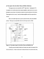
A 74138, which is a 3 to 8 decoder, was used to select the RAM, EPROM, the four
8255 I/O chips, and the 4 x 20 display. Using address lines A13-A15 from the 8052, it was
possible to take a 3 bit number (23=8) and make a unique, one of eight, output. The output
produced is low for the unique bit in question, with the other seven bits high. Since the chip
enables on the RAM and EPROM are ground true, this worked out well. For the display, this
'138 selective line had to be NOTed and then ANDed with a NOTed Write signal for a display
enable.
The 74138 is used very inefficiently in this design, but this is not a problem. Since it is
a 3-8 decoder, it can break RAM into eight different blocks. This gives 8 kbytes of memory
per block, but most of the components only use a few bytes to operate. The 8255 PIA uses 4
bytes, one byte for each port and the control word. The display uses only 2 bytes, the first for
the display instruction, the second, the display data. The display instruction sets up the format
of the display, while the display data actual pushes the character out to the LCD screen.
Excluding the RAM and EPROM, the whole board only requires 18 bytes of address
slots, and for this reason, flaws in the addressing scheme can be seen. However, for this
application, many separate address slots are not a requirement, and since there are only a few
external components used, this design does the job. If there was a need for more 8255's, A/D
52
converters, D/A converters, or displays, the addressing scheme could be optimized by
breaking down the RAM blocks even more by using another 74138. Table 3.2 gives the
component descriptions as well as their places in memory.
Table 3.2: The Controller Components and Their Place in Memor
Component Description
Breakdown
Address
Program Variable
8255 PIA (1)
Port A
02000H
BAI
Port B
02001H
BA1+1
Port C
02002H
BA1+2
Control Word
02003H
BA 1+3
Port A
04000H
BA2
Port B
04001H
BA2+1
Port C
04002H
BA2+2
Control Word
04003H
BA2+3
Port A
06000H
BA3
Port B
06001H
BA3+1
Port C
06002H
BA3+2
Control Word
06003H
BA3+3
Port A
OCOOOH
BA4
Port B
OCOOlH
BA4+1
Port C
OC002H
BA4+2
Control Word
OC003H
BA4+3
Display Instruction
OEOOOH
DI
Display Data
OEOOIH
DD
8255 PIA (2)
8255 PIA (3)
8255 PIA (4)
4x20 Optrex Display
53
8Kx8K
OOOOH
RAM
01FFFH
02000H
8255 PIA (1)03FFFH
255 PIA (3
04000H
05FFFH
06000H
07FFFH
EPROM
08000H
O9FFFH
255 PIA (2
NC
8255 PIA (4
OAOOOH
OBFFFH
OCOOOH
ODFFFH
4x20
OEOOOH
DISPLAY
OFFFFH
Figure 3.2: The Allocation of Memory in the pIPCircuit Design
Figure 3.2 shows the memory as it was allocated in this design. The address and data
lines to the RAM and EPROM were common, with a selection of each based on a chip enable
from the 138. Below is the wiring of the 74138 that allowed the memory mapping shown
above:
S A13 - AO
zA14 _ Al
A15-
A2
V+ -
1
V
O
E2
4x20 DISPLAY
8K RAM
---
8255PIA1
---8255PIA2
02
8255 PIA3
03 --- ·---- 8KROM
04
- NC
05
A
E1
+5V
+5V
-,,
E3
07
1I GND
06
--- 8255PIA4
Figure 3.21: The LS74138 Decoder
As mentioned before, there are more efficient breakdowns of RAM; one is shown below:
54
8K RAM
8K ROM
Figure 3.22: More Efficient Use of the 74138
the above design was developed by Joe Kujawa [6], and works in such a way as to dedicate
two, 8kbyte "chunks" to RAM and ROM (00 and 04 on the top 74138, respectively). The
first 74138 drives the second 74138 to dedicate memory from address locations 06000H to
06040H as memory that is broken into 8, 8byte increments. This design allows for 8 more
external devices, and the possibilities for even more breakdown of RAM can be seen.
In establishing terminology and for troubleshooting purposes, the following block
diagram was made of the pcb board design to give an idea were each block (as listed in the
memory mapping discussion) was located on the board:
55
DAC1
I I DAC
I
P-AMPS
OP-AMPS
I
DAC
I I DAC5
OP-AMPS I OP-AMPS I
Figure 3.23: A Block Diagram of the PCB Board Designed
The EPROM can be burned by creating a simple EPROM burning circuit using P1.4
and P1.5 from the 8052, and pin 27 (PGM) and pin I (Vpp) on the EPROM. This circuit will
be discussed later. The PROG 2 statement can be used when burning the EPROM, which sets
the baud rate automatically, and runs the first program encountered on the EPROM from initial
circuit power up.
56
3.3 The Display and Display Support Chips:
An LCD display (liquid crystal display), having four rows and 20 columns, was
included in the pcb design just in case initial instructions on power up of the unit needed to be
delivered. The LCD display was addressed at OEOOOH.
For the display, the data lines common to the RAM and EPROM were used to pass
information to the display. AO was taken to pin 4 of the display. A voltage divider was used to
vary the intensity of the LCD display.
7400 NAND gates were used to produce NOT gates and AND gates that were used in
transactions between the 8052 and the 573, RAM, EPROM, and display.
There are a few lines that need to be sent out as display instruction statements to
initialize the display. For this display, the following Basic 52 lines will do the trick:
DI=OEOOOH
hexadecimal.
The above sets the display instructionaddress as OEOOO,
DD--OEOO1H
hexadecimal
The above sets the display data address as OEOO1,
XBY(D)=OCH
The above turns the display on without a blinking cursor.
XBY(DI)=I
The above clears the display.
XBY(DI)--038H
The above is thefJ7ctions set. It callsfor 8 bit data length, 1/16 duty, aid a 5xlO dot
characterfont.
57
XBY(DI)=080H
The above sets the cursor at the homeposition.
Each particular LCD block has a different address assigned to it. For the 4x20 display,
the 4 lines of the display are addressed as follows (hexadecimal):
80: 81:82:
CO:
83 : 84:
85: 86: 87: 88: 89: 8A: 8B: 8C: 8D: 8E: 8F:90:91 :92:93
C1:C2: C3 :C4: C5 : C6: C7: C8 : C9: CA: CB: CC: CD: CE: CF: DO:D1 :D2 :D3
94: 95: 96: 97: 98: 99: 9A:9B:9C:9D:9E:
9F: AO: Al: A2 :A3 :A4:A5 :A6 :A7
D4: D5 : D6: D7 : D8: D9:DA:DB :DC :DD :DE:DF:EO:E1 : E2: E3: E4: E5: E6 :E7
.
.
Figure 3.3: The 4x20 LCD Display Address Map
To send a particular number or letter out to the display, the corresponding ascii number
needs to be written out to the display data address. For instance, if the number "8" needs to
placed at the fourth slot on the third line, the following lines would be written out:
XBY(DI)-097H
The above moves the cursor to the third line, fourth slot.
XBY(DD)=56
The above writes the ascii characterfor the number 8 out to the display data address.
Sometimes it is not desirable to be required to write out each individual character to the
display. If the initial instructions/statements to the manipulator users was to be:
You are using the TeradyreMagnum Manipulator.
then the following Basic 52 lines could be used to define the string, clear the display, set the
cursor at the home address (080H), and write the lines out to the display:
58
Table 3.3: A Sample LCD Display Program
STRING 2000, 21
$(0)-'You are using the"
(1)
(2)
$(1)="TeradyneMagnum"
(3)
$(2)="Manipulator"
XBY(DI)=1
(4)
(5)
XBY(DI)080H
(6)
FOR I=1 TO 17
(7)
XBY(DD)=ASC($(0),I)
NEXT I
(8)
(9)
XBY(DI)=OCOH
FOR I=1 TO 15
XBY(DD)=ASC($(1),I)
NEXT I
XBY(DI)=094H
FOR I=1 TO 11
XBY(DD)=ASC($(2),I)
NEXT I
(10)
(11)
(12)
(13)
(14)
(15)
(16)
(17)
The first line of the program sets up the memory allocation for strings. This gives 2000
bytes that will be dedicated for this purpose, with 21 bytes per string. Since there are only 20
slots on the display, this is more than enough. To calculate the maximum number of strings
that can be accommodated with this statement, the following formula can be used:
(#bytes/string +1)*number of strings +1 < # bytes allocated
From this statement, the maximum number of strings that can be defined is 90.
Lines 2-4 define the strings. The sentence was broken up so that each string would fit
on the 20 slot long display without a wrap around. It should be noted that if this "breaking up"
of the sentence was not done, line one would wrap to line three (on the display). Line two
would wrap to line four, and line four would then wrap to line one to overwrite the information
on this line.
Line 5 clears the display, and lines 6, 10, and 14 set the position of the cursor for
printing strings 0, 1, and 2, respectively. Three groups of statements found at lines 7-9, 11-13,
59
and 15-17 write out the ascii representation of strings 0, 1, and 2, respectively. The upper limit
of each "FOR" statement matches the length of each string.
"PUSH" and "ST@ (store at)" statements can be used to very quickly take information
in and then place it on the LCD display. Some sample code was written as an example of the
use of these statements. It should be noted that the following gives a display format for a
maximum form of "X.XXX" digits. This format can be changed to suit the resolution of the
transducer used for data acquisition.
60
-
Table 3.31: A Program to Use the Display and RAM Efficiently
__
-
10 NUM=temp
20 GOSUB 1000
1000 PUSH NUM
1010 ST@ 7300
1020 V=XBY(7300)
1030 V=V-126
1040 IF V<0 THEN LET V=0:XBY(7295)=0:XBY(7296)=0
1050 ON V GOSUB 1070,1085,1105,1125
1060 RETURN
1070 XBY(DISP)=48:XBY(DISP)=46:XBY(DISP)=48:XBY(DISP)=48:REMO.00X
1075 XBY(DISP)=INT(XBY(7295)/16)+48
1080 RETURN
1085 XBY(DISP)=48:XBY(DISP)=46:XBY(DISP)=48:
REM 0.OXX
1090 XBY(DISP)=INT(XBY(7295)/16)+48
1095 XBY(DISP)=(XBY(7295).AND.
15)+48
1100 RETURN
1105 XBY(DISP)=48:XBY(DISP)=46: REM 0.XXX
1110 XBY(DISP)=INT(XBY(7295)/16)+48:XBY(DISP)=(XBY(7295).AND.
1115 XBY(DISP)=INT(XBY(7296)/16)+48
1120 RETURN
15)+48
1125 XBY(DISP)=INT(XBY(7295)/16)+48:XBY(DISP)=46: REM X.XXX
1130 XBY(DISP)=(XBY(7295).AND. 15)+48:XBY(DISP)=INT(XBY(7296)/16)+48
1135 XBY(DISP)=(XBY(7296).AND.
1140 RETURN
15)+48
It should be noted that the PUSH and ST@ [5] statements need to be used
together. After specifyingthe number to be stored, an address destination must be given
with the ST@ statement. In the above sample program, an address location of 7300
decimal was chosen. This was completely arbitrary, but the address had to be high enough
that it did not interfere with the regular program storage in RAM. The number placed in
memory will be stored in "normalized packed BCD format" and will be stored in reverse
order from the starting address location.
61
The information stored at 7300 will be the number's exponent. The 8052 centers
this number exponentially about the hexadecimalnumber 080H, which corresponds to
1A0O. The number 081H corresponds to 10^1, 07FH to 10" -1, and so on. The
information stored at 7299 (the next bit in reverse order) will be the sign bit, with a 0
denoting a positive number, and a 1 denoting a negative number. The next four address
locations, 7298, 7297, 7296, and 7295 each contain two digits of the number, with 7298
corresponding to the lowest significantdigits.
The benefit of using this format of storing process data is that it is very efficient,
requiring fewer clock cycles than if each number was manipulated by stripping off each
individual digit. If the final algorithm that Teradyne comes up with starts bogging down in
calculations and the control loop time becomes too large, this can be used to make it more
efficient. If good programming is desirable, then this algorithm should be used, either
way.
62
3.4 The Signal Conditioning to the Counter Pins On the Microprocessor:
Originally, hall effect sensors were to be used for position feedback of some Thompson
actuators. This changed to stepper motors that were to be driven with the same oscillator,
which would provide synchronous, open loop movement for theta and in/out. When the hall
effect sensors were used, the signal was conditioned by amplifying it with an inverting op-amp
circuit and taking it to a schmidt trigger (inverting) which would clip it and make it a nice, clean
square wave signal.
Below is a block diagram illustrating how the hall effect sensors and various other
circuitry was to be used.
Figure 3.4: A Block Diagram of the System with Hall Effect Sensors
63
3.5 The AID Converters Used to Bring the Joystick Signals Into the Program:
The ADC804, an 8 bit analog to digital converter (255 steps), was used to convert the
0-5V voltage signal representing individual motor speed (desired) to a digital value to be taken
into the program running in the microprocessor. This package is a 20 pin DIP, 3 tenths of an
inch wide. The input voltage signal from the MSI potentiometers was taken to pin 6 of the
ADC0804. The output digital lines are labeled DB0-DB7 and are found from pins 18 to 11,
respectively. A 50 k.Q trim pot used as a voltage divider was used to feed a reference voltage
of 2.5 V into pin 9 of the ADC804. The "Read" and "Chip Select" pins of the A/D were tied
low (since they were ground true) so that the chip was always fUnctioning to make the
conversions. The "Write" pin was taken to an external clock (made from a 555 timer). It
should be noted that the Vref signals and the clock input signals on the five A/D's were tied
together. The 555 timer was wired up as shown below to provide the clocking signal to the
A/D converter:
4-
Figure 3.5: The 555 Timer Used For a Clock Signal to the A/D's
64
The 555 timer can be set up as an astable multivibrator, which means that it is an
oscillator, and does not need a trigger to produce a pulse. There are many different
characteristics of the oscillator that can be varied. For convention, the 330 ohm resistor can be
denoted R1, the 56 kohm resistor can be denoted R2, and the 22 uF capacitor C. The
following are the variables and limits of the 555 timer [15]:
Charge Time (output high):
0.693 (R1 + R2) C
Discharge Time (output low): 0.693 (R2) C
Period:
0.693 (R1 + 2R2) C
Frequency:
1.44/ ((R1 + 2R2) C)
Limits:
MaxR1 + R2 = 3.3Mohm
Min R1 or R2 = lkohm
Min capacitance = 500 pF
Max Capacitance = Dictated by leakage
Duty Cycle:
Time High/Time Low = (R1 + R2) / (R2)
Table 3.5 contains the values that were calculated from the resistance and capacitance
values used in this controller.
Table 3.5: The 555 Timer Circuit Values
Charge Time (seconds)
Discharge Time (seconds)
Period (seconds)
Frequency (Hz)
Duty Cycle
.859
.854
1.71
.693
1.01
It should be noted that after these values were selected and tried, the values were changed to
increase the frequency of the oscillator. The new values were:
R1 = 1 kohm
R2 = 5 kohm
C = 1uF
65
This gave new oscillator values of:
Table 3.51: The New 555 Timer Circuit Values
Charge Time (seconds)
Discharge Time (seconds)
Period (seconds)
Frequency (Hz)
Duty Cycle
.00417
.00347
.00764
130
1.20
,
As a general rule, R2 was chosen to be as large as possible with respect to R1 so that
the duty cycle would be as close to 1 (a symmetric square wave) while not decreasing the
frequency too severely.
The following is the manner in which the A/D converters were wired up:
10 kohm
AAA
VV
_
,
t
LO
Lo
I--
O
VCC
RD
CLKR
WR
DB0
CLK
V
0
CO l
00-
f~~~~I\
CS
1 OOpF
A_
jCL
>
DB1
INTR
DB2
WVIN A
DB3
-VIN
DB4
AGND
DB5
VREF
DB6
DGND
DB7
me
0
+15V
-+5v
8 LINE'
' TO 8255
I
Figure 3.51: The Wiring of the AD0804 Analog to Digital Converter
66
3.6 The DIA Converters and the Output Signal Conditioning:
A DAC0808 D/A was used to convert the controller action calculated in the program
(in the form of digital l's and O's)to an analog voltage. This voltage could then be signal
conditioned with some op-amps to produce an appropriate analog voltage to the motor
amplifiers. The D/A that was used was an eight bit D/A, with 255 steps possible in conversion.
It is a 16 pin DIP package, 3 tenths of an inch wide. The input digital lines are pins 5 through
12 on the package, and are labeled DAO-DA7, respectively. It should be noted that the
specification sheet from National Semiconductor labels the most significant bit as DAO and the
least significant bit as DA7, which seems exactly reverse of the normal pattern of labeling I/O
lines.
The chip takes a digital input value between 0 and 255 to an analog voltage ranging
between 0 and -10OV.Originally, two op-amps (741) are used to signal condition this to a plus
or minus 10 V signal commonly used as inputs to a motor amplifier, but these resistor values
can be changed to suit the amplifier that is selected. For the stepper system, resistors would be
selected to give a 0-5V signal out, and for the UDC-800, a 0-1OV signal would be produced.
It should be noted that when talking about TTL logic levels, a low signal ("0") varies between
0 and about .8V, and a high signal ("1") is usually above 2.0 V. Anything in between these
values is considered a "float" or a "tri-state," since it can go either way in interpretation, and
can cause problems with I/O data transfer. Pull up or pull down resistors need to be used to
correct a float condition, but luckily, these problems were not encountered with this circuit.
67
Each D/A converter that was used was wired up in a particular manner; this is shown
below:
I -15v
/3 " 0.1uF
-15V
NC
CMP
GND
VREF-
VEE
iACID
I
+15V
VREF+
O
TO SIGNAL
CONDITIONING
5.1 kohm
5.1kohm
VOUT 0
VCC
-+5V
DAO I=
DA7
I en
DA1
DA6
DA2
DA5
DA3
DA4
uF
I
--(
8 LINES TO 8255
Figure 3.6: The DA0808 Digital to Analog Converter
The circuit shown below was used to signal condition the output from the DAC0808
to the motor amplifiers. The output from the D/A is a voltage signal that ranges from 0 to -10
V, and this converts it to a signal that ranges between -10OVand +10OV.
·,..* 5v
qJ .
rv
20 K
0 to +10V
0 to -10V
ifiers
10 K
K
Figure 3.61: The Output Signal Conditioning
68
The first op-amp circuit just inverts the 0 to -10 V signal to produce a 0 to +10V
signal. The second op-amp is set up in the differential configuration, and the output can be
related to the difference between the input voltages multiplied by the gain:
Vout= (RfRi)*(Vb-Va)
For this setup, the ratio of the feedback resistor to the input resistor is 2 (20k/10k), and the
voltage Va is always +5V. Vb is the voltage that ranges between 0 and +10OV.For Vb=OV:
Vout-(20k/10k)*(0-SV)
Vout= -10V
For Vb= +10V:
Vout=(20k/10k)*(1 0V-5V)
Vout= +10V
One problem that was encountered when writing the software to control the motors of
the system was the fact that the D/A converters only recognize a number between 0 and 255,
not one that varies between plus or minus 128. When negative digital values were sent out, the
program crashed and gave an error statement that did not directly indicate what had happened.
This is mentioned in case someone tries to write programs for this controller down the road.
Signal conditioning of the actual digital control signal had to be performed to give 0-255
representing -1OV to +10OV,respectively.
69
3.7 The 8255 PIAs Used For I/O to the DlA's and From the A/D's,
Respectively:
The A/D and D/A data transfer, as well as some switching to some motor relays, was
accomplished through the use of an 8255 PIA. The 8255 is a 40 pin DIP, 6 tenths of an inch
wide. This is a device that inputs and outputs digital values and can be addressed by the
microprocessor in a controller program. The 8255 has 3 ports (A, B, and C) that can input or
output 8 bits of data. In the circuit built, the four 8255's were addressed at 02000-02003H,
04000-04003H, 06000-06003H, and OC000-OC003H, respectively. Port A had the first slot
in each address group, with ports B and C occupying the second and third slots, respectively .
The fourth slot was reserved for the control word. The control word had to be sent out in the
Basic-52 program to initially setup which ports would be used for inputs and which ones would
be used as outputs.
It should be noted that the read, write, Al, AO, and D0-D7 lines to all of the 8255's
were wired in parallel, while the chip enable bits of each 8255 had a unique chip select line
from the 74138.
The control word for the 8255 sets up the ports as either input or output.
It can break up port C into two, 4 bit ports, or keep it as one, eight bit port for input and
output. The control word is defined as follows:
1
0
0
128
64
32
PAO- PC4PA7 PC7
16
8
0
4
PBO- PCOPB7 PC3
2
1
For the 4 port setup bits, a "1" is used for input, and a "0"
sets up the 8255 port as output.
70
It should be noted that the bits that have numbers in them should remain at these set
values; only bits 0, 1, 3, and 4 should be manipulated. The control word only needs to be
written out to the 8255 once after power up. An example of the Basic 52 statement that would
do this for the first 8255 (see memory mapping explanation) and set it up as input for ports A
and B and output for port C would be:
XBY(02003H)=146
The above expression has a hexadecimal address and a binary number written to the address.
To simplifythe programming, the base address for the first 8255 is defined as:
BA1-=02000H
This simplifies the program statement, which can be written as:
XBY(BA1+3)=146
71
3.8 Design Considerations For Microprocessor Board Improvement:
There were many things that were seen that could be added or removed to improve the
functionality of the microprocessor circuitry. One idea that came to mind was using a bit off of
an 8255 PIA to switch between +5V and ground to be used as the oscillator signal to the
stepper motors. This would have three extremely kick ass results: Two oscillators would be
removed, saving money and space; there would be no need for feedback of the oscillator signal
to give an idea of position; and the microprocessor could vary the signal in as small of an
increment as desired. The steppers require 200 pulses from an oscillator for one rotation of the
shaft, which gives 1.8 degrees per pulse. Since the lead of the screw on the carriage is about 8
turns per inch, the stepper shaft must turn 8 times to get one inch of linear travel. The radius of
the manipulator head is 15 inches, and from this information, an angle can be calculated for the
theta motion per pulse of the oscillator.
...-.15"
.
A
-o0: . .............
I
A
i
I
I
'Y""""'
I
I
i I
LI
Figure 3.8: The Resolution of the Theta Axis
The above picture is drawn with exaggeration to illustrate a point. The delta indicates
the linear travel of the carriage assembly per oscillator pulse. This is calculated as follows:
72
A=
(shaft rotation/pulse)(linear travel/shaft rotation)
A=
(1.8 degrees of rotation/pulse)(1/8 "/rotation)(1 rotation/360 degrees)= .000625"/pulse
This number is then multiplied by two since each carriage actuator produces this travel:
A' =
.00125"/pulse
The angle that the manipulator actually turns in theta motion for each oscillator pulse will then
be:
0=
arctan(.00125/15)=
.004775 degrees/pulse
The above angle is actually the worst case angle in that as the theta angle approaches the 2
degree limit set by Teradyne, this angle/pulse measurement will go down. This large angle
increment is only seen when the theta angle is near zero, or, in other words, the testhead is
centered in travel in the carriage roller bearings.
The purpose of this calculation is to show the degree of control that could be
implemented if the microprocessor was used. The microprocessor can produce a pulse signal
that varies between 0 Hz up to the inverse of the program loop time (some fraction of 1 Mhz).
This means that a "resolution" knob could be added to the joystick that would act as a
multiplier of the joystick action. It would actually vary the sensitivity of the action, giving a
very precise response by outputting a small frequency range of oscillator signal at low
multipliers, and large frequency ranges at high multipliers. This could be set at a very high
range for quick responses when the testhead is initially orientated to the docking area, and set
to low ranges when the final docking corrections were being made to get a "nuts on" dock. In
fact, this range could be varied automatically through the use of a proximity sensor so that as
the testhead approached a dock, the sensitivity ofjoystick action would be reduced.
73
This change would only remove a small fraction of the total cost of the manipulator
overall, but it would greatly reduce the packaging of the electronics cabinet. The two 12 gauge
wires carrying the 13 VAC to each oscillator would be eliminated, as well as the two oscillators
themselves. This would also get rid of 16 I/O lines used to run two, 8 bit D/A converters used
to vary the oscillator output. In addition, the need for feedback of the oscillator signal would
be eliminated since the microprocessor would definitely know what was sent out.
The microprocessor could be programmed to know the number of pulses
corresponding to full stroke on the carriages, so exact positioning could be given on the LCD
display. This would likely be nothing more than a novelty, but customers usually appreciate
novelties that save them money.
74
CL~
DIACS
0- \ \ \ \=LLL
\
001U4*-O\:2,nojq::~oN
(¢C, =blcaRQS3<C<
QQR0+F<aaacafiLL
8k
10k
:
S
7Y
nn'
J cl-1
5sk
A:
r
_CDsn
n = E
-1
___
___I
_I
-I-4
2550k
1
EOk
..
j'0k
5
554
<
Q~"~"
0
I-
l sp] ay
I
2Ok
10k
nk
=
0
-.
Ac
3k
1Ok
=k
0
u
aKXBK
Icli
jOt
0
EOD
!0k
iOk
Yin
I" ;
oJ
10k
O
I-
u
nk
OW
I
5
C::
EOk
_
t.
O
0
Qp
U
_
rr
p0
0Q
(2
X
M
'4
O
n
N
-V
ihi
cc
Cr
i
)
Ji
?is
74573
rn
'U)'
i
0
Ir
0
tJ
U)
ti
-
--
-
-'
--
n
5
I.)
n
r
Nc
n
-
C
oJ
co
<Z
La
D
=
LN
1L
I.q,
o
ei
-
7
L
n
.4
tu
0
Jo
PORTI
lu
1U
Sk
5R
mj
Ra
L nd
L
Doub eda j Jr
10
Q
*0
4
Lu
02
0
ao
Q)
L.
-
cc
04
QS
00.
E
04
.
.C
cr,
izu
II
lea
la
C
rN-
I..
to
C
as
3.9 Troubleshooting
the PCB Board Design:
There were several considerations taken when troubleshooting each block of the
pcb board. Two prototypes were made by AP Circuits Limited in Canada. These were
made from gerberized files produced from the Wintek designs I made of the controller
board. The prototypes came back with some traces that were offset, and the angle of
offset pointed to a manufacturing error. To correct these errors, traces were physically
cut, and very small gauge wire was used to create jumpers for the cut traces that happened
to touch.
The first board was populated very quickly with parts, due to an overzealous
designer, and a mistake in soldering must have occurred. The result was a board with
roughly nine hundred connections running at 11.0592 Mhz (in other words, a bear of a
troubleshooting job). After spending about 60-70 hours of troubleshooting and making
very little forward progress, a different approach was taken. The second board was
populated with only the basic microprocessor circuitry (8052, RAM, 74573, 74138,
clock), and it's functionality checked. The problem with this trial was that the wrong
value of resistor was used for the reset circuit. A 4.7 uF capacitor was originally used in
series with a 100 kf to provide reset. This circuit could also be called a "Reboot" circuit
in that it is required for the system to work at all. A friend in Montana was consulted, the
board shipped to him for inspection, and after replacing the 100 kf resistor with a 1 kf,
the basic microprocessor circuit worked without problems.
The next step in the development of this second prototype board was to populate
all of the parts that operated with +5V. This approach seemed reasonable in that a lantern
battery could be used to power the circuit, as opposed to the 70A supply normally used
78
that provided plus or minus 5V and plus or minus 12V. This power supply was
partitioned, but still provided several amps per partition, and had a tendency to catch
components and boards on fire if miswiring occurred.
In keeping with this strategy, the sockets for the 8255 PIA's were soldered in, the
8255's placed in the sockets, and a simple program written to check each of these I/O
chips. Since the chips can be used as either input devices or output devices, or a
combination of both, two programs were written; one to test the use as an input device
and the other as an output device. For the output device program, the user could enter a
number between 0 and 255, and the equivalent binary representation would appear at each
of the three ports of each of the four 8255s. A logic probe was used to quickly check
each port to make sure that the number was actually making it that far.
For the input program, +5V or ground could be taken to the eight bits of each
port and checked on the computer display. The computer displayed the decimal
equivalent of the binary number, and for this reason, it was easiest to just take one bit
high at a time (ie, 1,2,4,8,16,32,64,128
would be seen). These two programs can be
found on the following two pages.
79
3.9: PROGRAM TO CHECK 8255'S AS OUTPUT DEVICES:
Table
-----10 REM THE FOLLOWING IS THE 8255 INITIALIZ TION
15 REM BAI DENOTES THE BASEADDRESS OF THE FIRST 8255, AND SO ON
20 BA 1=02000H
30 BA2=04000H
40 BA3=06000H
50 BA4=OCOOOH
55 REM THE FOLLOWING SETS UP THE 8255 'S PORTSAS OUTPUT PORTS
60XBY(BA 1+3)=128
70XBY(BA2+3) =128
80XBY(BA3+3) =128
90XBY(BA4+3)=128
120 REAMBA +3 IS THE CONTROL WORD
130 REM BA +2IS PORT C (HEREOUTPUT)
140 REM BA +1 IS PORT B (HERE OUTPUT)
150 REI BA +0 IS PORTA (HERE OUTPUT)
155 REM 155 ALL INPUT 128 ALL OUTPUT 144 MIX
157 REM ENTER THE DECIMAL EQUIVALENT OF THE NUMBER (0-255) THAT YOU
158 REMf IVANTAS OUTPUTA T THE PORTS OF THE 8255
160 INPUTA
165 REMA [WILLNOW BE WRITEN OUT TO ALL THREE PORTS OFALL FOUR 8255S
170 XBY(BA 1) =A .B Y(BA I + 1) =A :XBYB4 1 +2)=A
180 XB Y(BA 2) =A :XB Y(BA 2 + 1) =A :XB Y(BA 2 +2) =A
190 XB Y(BA3) =A :XBY(BA 3 +1) =A .XB Y(B3 +2) =A
XBY(BA 42)=A
4+2)=A:XBY(BA
200 XBY(BA 4) =A:XBY(BA 4+
400 GOTO 160
Table 3.91: PROGRAM TO CHECK 8255'S AS INPUT DEVICES:
10 REM THE FOLLO IiNG IS THE 8255 LVITIALIZATION
15 REM BA I DENOTES THE BASEADDRESS OF THE FIRST 8255, AND SO ON
20 BA I =02000H
30 BA2=04000H
40 BA3= 06000H
50 BA4=OCOOOH
55 REA THE FOLLOIING SETS UP THE 8255 'S PORTS AS INPUT PORTS
60 XB (BA 1+3)=155
70XBY(BA2+3)=155
80XBY(BA3+3)=155
90XBY(BA4+3)=155
120 REAl BA +3 IS THE CONTROL WORD
130REMABA +2IS PORT C (HEREINPUT)
140 REA BA +1 IS PORT B (HERE INPUT)
150 REM BA +0 IS PORTA (HERE INPUT)
152 REM USING +YV TO INDICA TEA "1 "AND GROUND (OJ0ASA "0", HARDWIRE THE
154 REM APPROPRIA TE BINARY NUMBER TO THE PORTS OF THE 8255S
165 REA THE BINARY NUMBERS TAKEN TO THE PORTS (A,B,Cj WILL NOW BE READ INTO THE
167 REM VARIABLESA-L
1 70A =XBY(BA1):B=XBY(BAI +1):C=XBY(BA1+2):D=XBY(BA2):E=XBY(BA2+1):F=XBY(BA2+2)
190 G=XB Y(BA3):H=XB Y(BA3 +1):I=XB Y(BA3+2)
200 J=XBY(BA4):K=XBY(BA4+ I):L=XBY(BA4+2): PRINTA,B, C,D,E,F,G,H,I,J,K,L
220 GOTO 170
80
After the 8255's were up and running correctly, the next logical step was to install
the Optrex LCD display. This display is powered with +5V and ground, so it could also
operate off of a lantern battery. This move had the added advantage in that it gave
feedback on the condition of the rest of the circuit. If the LCD blocks were not lit, it was
an indication that something within the circuit was going sour between +5V and ground.
For timing purposes, a 7400 Quad Input Nand Gate chip was used to create an
AND gate with two NOTed inputs. The chip select from the 74138 and the write line was
taken to each of these NOTed inputs, and the output was taken to pin 6 of the Optrex
display. These signals are mentioned in that these have the most probability in causing
problems for the display. Pins 7-14 on the display are the data line inputs (D0-D7). Pin 4
of the display is the A0 input line. When this line is low, the display is receiving a display
instruction (DI), and when it is high, it is receiving display data (DD). In troubleshooting,
these pins (7-14 and 4) should be seen strobing at a very high frequency. This can be
checked with a logic probe that has the pulse feature.
Pins 1 and five should see ground, and pin 2 should be at +SV. The voltage at pin 3 can
be varied to change the intensity of the screen, or it can be shorted to pin 1 to give the
darkest screen possible.
A mistake was made on the pcb design in that pin 3 was left to float, but was easily
corrected by taking a jumper wire from pin 1 to pin 3.
It should be noted that each size display that is sold by Optrex will vary in the
address locations assigned to each LCD block. Also, the function set for each as well as
the other initialization instructions will vary. The code written is an example of a 4x20
81
display and cannot be used on another display, such as a x16. Optrex can be consulted
for a specification sheet that will "memory map" each display.
The following can be used as a diagnostic test of the functionality of the Optrex
4x20 LCD display:
Table 3.92: PROGRAM TO CHECK OPTREX LCD DISPLAY:
S REM 10 - 60 ARE DISPLAY INITIA4LIZATIONCOMMANDS
7 string 400,20
8 $(0)= " WEL COME TO THE' :$(1)="TERADYNE MAGNUM"
9 $(2)="MANIPULATOR"
10 DI=OEOOOH
20 DD=OEOOIH
30XBY(DI)=038H
40XBY(DI)=OCH
50XBY(DI)=083H
60XBY(DI)=I
1
65 XBY(DI)=080H
70 FOR I=1 TO 14:XBY(DD)=ASC($(O),I):NEXTI
75 XBY(DI)=OCOH
80 FOR I=1 TO 15:XBY(DD)=ASC($(1),1):NEXT I
85 XBY(DI)=094H
90 FOR 1=1 TO II:XBY(DD)=ASC($(2),I):NEXT I
100 FOR J=l TO 500:BY(DI)=8:NEXTJ
120 FOR J=1 TO 500:XBY(DI)=12:NEAT J
130 GOTO 100
On the following page can be found a routine that was written to automatically
calibrate the input signal conditioning. It finds the range of the voltage signal generated by
the MSI potentiometer, and "zero and spans" this signal in software.
This routine reduces the pcb design by three op-amps and two trim pots per input
voltage. Since there are five input voltages brought in through A/D converters, this gets
rid of 15 op-amps and 10 trim pots. This is a significant reduction in the size of the pcb
board.
The limitation of this approach is that is requires the user to "stroke" each
potentiometer on the joystick through a full range of motion. However, this stroking
82
could be done when the manipulator was assembled, and these stroke values could be
permanently burnt into the EPROM. The program has some deadband included so that
slop in calibration will not give a turning motor with no joystick command.
83
Table 3.93: Program to Automatically Range the Potentiometers
5 REM 10 - 60 ARE DISPLAY INITIALIZATION COMMANDS; REM INPUT S
10 DI=0E038H:DD=OE039H:XBY(DI)=038H:XBY(DI)=OCH:XBY(DI)=083H:XBY(DI)=1
70 REM THE FOLLOWING IS THE 8255 INITIALIZATION
80 BAl=OE028H:BA2=0E030H
100 XBY(BA1+3)=144:XBY(BA2+3)=155
120 REM BA+3 IS THE CONTROL WORD
130 REM BA+2 IS PORT C (HERE INPUT)
140 REM BA+I IS PORT B (HERE INPUT)
150 REM BA+O IS PORT A (HERE INPUT)
155 REM 155 ALL INPUT 128 ALL OUTPUT 144 MIX
160 REM BA1 DENOTES THE BASE ADDRESS OF THE FIRST 8255
170 REM BA2 DENOTES THE BASE ADDRESS OF THE SECOND 8255
175 q=l:TA=255:TB=255:TC=255:TD=255
177 BA=O:BB=O:BC=O:BD=O
180 a=xby(bal):b=xby(ba2):c=xby(ba2+1):d=xby(ba2+2)
183 xby(bal+l)=e:xby(bal+2)=e:rem output to DAC
185 f=portl .and. 1:g=portl .and.2
186 if f<>l then fr=l1
187 if g<>2 then fr-O
188 if f+g=3 then fr=10
189 REM SAVES THE MINIMUM VALUE OF THE INPUT
190 IF A<TA THEN TA=A
191 IF B<TB THEN TB=B
192 IF C<TC THEN TC=C
193 IF D<TD THEN TD=D
200 REM SAVES THE MAXIMUM VALUE OF THE INPUT
201 IF A>BA THEN BA=A
202 IF B>BB THEN BB=B
203 IF C>BC THEN BC=C
204 IF D>BD THEN BD=D
210 REM CALCULATES THE RANGE OF THE INPUT
211 RA=BA-TA:RB=BB-TB:RC=BC-TC:RD=BD-TD
220 IF RA=OTHEN RA=1
221 IF RB=O THEN RB=1
222 IF RC=OTHEN RC=1
223 IF RD=OTHEN RD=1
250 IF RA>3 THEN A=(A-TA)-(RA/2) ELSE A=O
255 IF RB>3 THEN B=(B-TB)-(RB/2) ELSE B=O
260 IF RC>3 THEN C=(C-TC)-(RC/2) ELSE C=O
265 IF RD>3 THEN D=(D-TD)-(RD/2) ELSE D=O
270 A=(2*A/RA)* 10:B=(2*B/RB)*10
280 C=(2*C/RC)* 10:D=(2*D/RD)* 10:e=-((((10-d)/20)*255))+255
283 REM CALCULATE THE INCREMENT
285 IA=RA/255:IB=RB/255:IC=RC/255:ID=RD/255
290 A=(INT(A* 10))/10:B=(INT(B* 10))/10:C=(INT(C* 10))/10:D=(INT(D* 10))/10
300 IF ABS(A)<(5*IA) THEN A=O
302 IF ABS(B)<(5*IB) THEN B=O
304 IF ABS(C)<(5*IC) THEN C=O
306 IF ABS(D)<(5*ID) THEN D=O
307 IF ABS(A)>I.AND.ABS(C)>1 THEN ANGLE=1 ELSE ANGLE=O
395 print "
400 goto 180
",a,"
",b,"
",c,"
",d,"
",fr,"
",ANGLE
84
3.10 Quadrature Decoding:
An encoder, which is a requirement of coordinated movement of the side/side axis
with the up/down axis, generates two square waves that are out of synchronization. The
frequency of the signal is proportional to the speed of the motor, and the phase gives
directional information. A counter can be used to accumulate the pulses of this square
wave generator to give an idea of position, but this information is meaningless if the motor
changes direction, since it will accumulate forward and reverse pulses without
discrimination. To avoid this, the following digital circuit was designed to decoder these
signals and produce a TTL signal that indicates the direction of rotation. This logic
involved the use of four AND gates, two NOT gates, and three RS reset precedent
latches.
The extremely cool reality here is that this logic can be totally implemented with
Basic 52 statements, and the 8052 has two, sixteen bit counters to accumulate this
function. This gives two channels of quadrature decoding for each 8052 microprocessor.
The limitation of this logic is that the counters can only accurately monitor a signal less
than 1/24 of the clock frequency, or about 500 Hz. The following is the code that can be
used for quadrature decoding. It should be noted that the signals A and B need to be
brought in through an I/O port, such as port l.
85
REVERSE
FORWARD
A
A
B
B
L FL
K
L
V
I
B
Figure 3.10: TTL Equivalent of the Quadrature Decoding Program
86
Table 3.10: Quadrature Decoding Program
10 REM BEGINNING OF LOOP
20 A=PORT1.AND. 1:B=PORT1.AND.2
30 S 1=A.AND.NOT(B):S2=NOT(A).AND.B:R1=S2:R2=S
1
50 IF Sl=l THEN Q=l
55 IF S1-0 THEN QI=Tl: REM MEMORY
60 IF Rl=l THEN QI=0
65 TI=Ql
70 IF S2=1 THEN Q2=1
75 IF S2=0 THEN Q2=T2: REM MEMORY
80 IF R2=1 THEN Q2=0
85 T2=Q2
90 S3=A.AND.Q1 :R3=B.AND.Q2
100 IF S3=1 THEN Q3=1
105 IF S3=0 THEN Q3=T3: REM MEMORY
110 IF R3=1 THEN Q3=0
115 T3=Q3
120 FORWARD=Q3
125 REM PLACE COUNTER ROUTINE HERE; BASED ON FORWARD SIGNAL, ADD OR SUB.
126 REM THE COUNT SIGNAL TO THE ACCUMULATED VALUE, THEN RESET THE COUNTER
127 REM TO ZERO
130 GOTO 10
87
Chapter 4: The Pushbutton Logic
4.1 The High/Low Speed Circuitry
The following circuit was used to give two speeds for the up/down and the twist
axes. This is nothing more than two voltage divider circuits that are switched between
using a DPDT pushbutton. When the button is not pressed, the voltage to the UDC 800
card (S2) is created from the ratio of RI and R2 using the normally closed set of contacts
on the pushbutton. When the button is pressed, the voltage to the card is from the
resistors R3 and R4. In the beginning, the two cards were tied in parallel between the S 1,
S2 and S3 terminals. It was thought that this might be detrimental to the boards if the two
boards did not have the same S3 voltage (+12V). The line connecting the two cards at
q II
.... S3(GND)
NC
NO
R1
R3
NCC
NO
1t2
R4
Si (ND)
S2
7
Figure 4.1: The Circuitry for the High/Low Speed
88
their S3 terminals was removed for this reason. The circuit shown below was also used
with the EPROM circuitry to control the speed of the Bodine and Bison motors.
89
4.2 The Logic to Run the Up/Down and Twist Axes
In the beginning, there was the idea that the motors would be driven up against a
mechanical stop and the user would hear the change in motor sound and stop running the
motor in that direction. The only reason this was even considered was because of the cost
driven nature of this project. Limit switches were always desirable, but were an added
cost to produce the manipulator. The logic that was initiallyused to control the up/down
and twist axes is shown below. This does not include limit switches.
RI: UP/DOWN I
R2: UP/DOWN (
R3: TWIST DIRt
R4: TWIST ON/OFF
Figure 4.2: The Ladder Logic for the Vertical and Twist Axes
This logic is nothing more than the reproduction of AND and OR gates through
basic switching paths. If the enable button is not pressed, the current from the 24 V
supply does not flow at all. If pressed, the normally open contact closes and juice is
delivered to the top side of the up, down, twist cw and twist ccw pushbuttons. The on/off
90
relays for the up/down and twist axes will energize if either of their respective buttons are
pushed. This is the equivalent of OR gate logic. Directionally, the system is set to go up
and counter clockwise in twist without any of the directional relays energized. The down
pushbutton is pressed to energize R1 and give down direction, and the twist cw button is
pressed to energize R3 and give clockwise direction.
The relays mentioned are just DPDT, form CC relays from Potter & Brumfield.
Dynamic Braking is achieved by placing a 25f resistor between the motor leads in the off
position. The physical hookup of the up/down relays (R1 & R2) is shown below. It
should be noted that the twist relays (R3 & R4) were wired in the same manner:
Ri
i
Leads
I
Figure 4.21: The On/Off and Directional Switching
Dynamic breaking was included to prevent the motor from coasting to a stop.
Even without load, the motor coasted, and it was thought that the added inertia from a
testhead would even make this problem worse.
91
4.3 The Logic to Run the In/Out, Theta, and Side to Side Axes
The stepper motors were controlled with TTL logic levels. A high signal (+5V)
was applied to the on/off terminal of the Anaheim amplifierto make the motor turn, and a
high signal was also taken to the direction terminal to reverse the direction of the rotation.
These signals were low current, since the Anaheim amplifier would only output about a
100 mA.
Below is the ladder logic that was used to control the in/out, theta, and side/side
motions. This logic was created before the limit switch logic came into effect:
Man. Side/Side
Clockl
&
Man. Theta
m3
Pulse
r/"-,~,~ ~t^,,lt}
I
;ai
C
i1UVl
I
.I[L
Manual Side
(".1
'n1;I.
J1U; .ill.
r
-
ull.UUlI
-,bI-~, _ OnI
11
_.._.
Enable
I
U.---1
A
~~-Tft~-rI
In
I
Out
Man. Theta
Enable
I
Out
I
TR
11
Out
I
On2/3
4Direction 2
I
Direction 3
II1
V
Figure 4.3: The Ladder Logic for the In/Out, Theta, and Side/Side Axes
Normally open and normally closed sets of contacts were used in the control of the
in/out and theta axes. There are some sets of contacts that had to be used more than once,
92
sometimes many more times than once, and for this reason, 4PDT pushbuttons were
selected.
Looking at the signal "ONI," it can be seen that by pressing either the side left or
side right pushbuttons will make this high, turning the side stepper on. Of course, the
enable has to be pushed, or this line will always be connected to a low. The low signal
was referenced from the low side of the external pulse generator, which was connected to
the common ground of the system. Also, the "Manual Side" pushbutton must not be
pressed to get the side stepper running.
The manual side pushbutton was used to get compliance for the stepper motor.
Contacts are used off of this pushbutton to break the oscillator signal to the clock input on
the stepper amplifier as well as keeping the stepper motor de-energized. However, it was
later realized that it is possible to turn the shaft of the stepper motor in this state, but when
the lead screw is added to the system, the torque required to "break the step" is so high
that the system is essentially not back driveable. This sled to the decision to add electric
clutches to the stepper drives that would be engaged when the motors were driven, and
disengaged to get compliance.
The problem with this logic used to control the stepper motors came when more
than one pushbutton was pressed. If both the theta left and theta right pushbuttons were
pressed together, then it would give the equivalent of out motion. Problems also came in
with the addition of limit switches when a certain combination of pushbutton presses
would actually bypass a "made" limit switch.
93
4.4 The Addition of Limit Switches
When it was decided to add limit switches to the system, some logic was decided
upon to accomplish it. For the up/down, twist, and side/side axes, it was fairly simple.
The logic was set up to allow motor operation until a limit was hit, and then only allow
operation of the motor in the reverse direction. This logic was designed before the
compliance limit switches were added to the control of the up/down axis.
Below is the logic designed to implement limit switches on the up/down axis. This
logic is identical to the logic used for the twist axis, except that it uses a different set of
limit switches. This logic was added in series to the on/off relays controlling the up/down
and twist axes and would act to break the line energizing these relays if conditions were
not met.
It should be noted that series connections can be seen as AND gates, and
parallel combinations can be seen as OR gates.
PB Up
PB DowNn
PB Donm
PB Up
On
LS Up
LS Down
Figure 4.4: Limit Switch Logic For the Up/Down and Twist Axes
If the up limit switch is made (LS Up), then the only way the on relay will energize
is if the down pushbutton is pressed and the up pushbutton is not pressed. If the down
limit is reached (LS Down), then the only way the motor will run is if the up pushbutton is
94
pressed and the down pushbutton is not pressed. If these words are analyzed, it can be
seen that normally closed contacts can be seen as NOT gates.
The side to side logic, although exactly the same reasoning, is wired up differently.
This is due to a motor that runs if the signal is taken away. A ground or a "0" must me
applied to the on terminal of the stepper amplifier to turn the motor off. The following is
the logic that was used to run the side to side stepper. Since this case is different in the
way the motor is turned off, this logic was placed in parallel with the "on" signal shown
earlier for the side to side stepper.
LS Right
PB Left
Figure 4.41: Limit Switch Logic For the Side to Side Axis
If either of the limit switches in the above circuit are made, a "0" is pushed through
to the on terminal turning the motor off. If the right limit switch is made, then the motor
will only run if the left pushbutton is pressed and the right pushbutton is not pressed. In
this case, due to the backwards logic to run the stepper, and AND gate is produced from a
parallel combination. The left limit switch works in a similar fashion.
95
The limit switch logic for the in/out and theta axes was the most complicated to
produce. In preparing the logic and without having any idea as to how the limit switches
would be mounted, limit switches were picked to be mounted at the extreme end of each
carriage motor rail. Looking at the testhead from the top, the following is how the limit
switches were to be positioned in the beginning.
I
In
I
I
I
Theta Left:
Theta Right: Clockwise Rotation
Figure 4.42: Expected Limit Switch Mounting on the In/Out and Theta Axes
It was thought that if limit switch M was "made," only "in" motion or theta left
motion would be allowed to correct the situation. If 2M was made, only in motion and
theta right motion would be allowed. If 3M was made, only out motion and theta right
motion would be allowed, and in the same manner, if 4M was made, only out and theta
left motion would be allowed. Although this is very tedious to explain in words, it is even
more tedious to reproduce it electrically.
This logic can be reproduced using 4PDT pushbutton contacts, but since the
pushbuttons have a common point between the normally open and normally closed
contacts, some real organizational problems exist. The limit switch logic shown can be
placed in parallel with the ON2/3 signal to the in/out and theta stepper amplifiers.
Without words, this figure best illustrates the reason we switched from pushbutton logic
to EPROMs for motor state control.
1M
IN PB
TL PB
ON2/3
Figure 4.43: The Limit Switch Logic For the In/Out and Theta Axes
97
As can be seen from this chapter, pushbutton logic is a possibility for the
manipulator control, but was an extreme reaction to the revulsion to any complexity in
circuitry. The irony in this is that to avoid complexity, we developed a situation where
seven or eight contacts from each pushbutton were to be wired in a complicated scheme of
series and parallel combinations. The futility of this design was seen after troubleshooting
for about 24 hours straight. The system would work for a while, and then one of the
many wires of contact interconnection would touch, and one piece of the logic would stop
working. Then, when troubleshooting to get this part working, another would fail.
Although it goes against the grain to give up when troubleshooting, this was almost a
ridiculous solution when one actually thought about it. This led to the EPROM idea, and
it has proved to be a fairly large improvement over using pushbutton logic to control the
axes of the manipulator.
98
Chapter 5: Control Through EPROMs
5.1 Circuitry
The idea to use EPROMs to monitor the pendent and limit switches came as a direct
result of pushbutton switching logic that was too complex. In a meeting with R.P. St. Clair
and Frank Parrish in which the pushbutton logic was checked, it was noticed that although the
logic worked well if only one pushbutton was pressed, there were some problems with
direction of the stepper motors if more than one pushbutton was pressed.
This led to the suggestion to use the EPROMs, and so far, it has seemed a fairly good
suggestion. When the logic changed, and it changed almost every day, a new set of EPROMs
could be programmed instead of having to rewire the controller. Three EPROMs were used,
with one controlling the in/out and theta axis, another controlling the up/down and twist, and
the third controlling the side/side motion.
A fourth EPROM will be employed in a later design to prevent the system from
recognizing more than one pushbutton press. As it sits, the up/down and twist axis cannot be
operated together, but this not prevent the side/side, in/out, or theta motions being actuated at
the same time. This fourth EPROM will work in such a way that if one pushbutton is pressed
that is an input to a particular EPROM, the other EPROM's chip select lines will be taken high
deactivating them.
The Am27C128, 8x16k EPROM was selected for this circuitry [7]. This EPROM is a
CMOS chip that can be erased with ultraviolet light in a matter of minutes, and can be
programmed in even less time. The access time for each word that is stored in memory is less
than 55 nanoseconds, which is probably a lot quicker than a solid state relay can change state.
99
I
-
a
I
-
_
-
-
I
--
·
!
U
-
-
.
-
-·-L
-- --
.
I
_
o
i
I
4
14
I .- -1
I--T 1
I I
I
I I
-
9
f,-TLI
I
I
4
I
11 1.
II -- i-oo-4 9
I
'.
I 2
I
I I
I I
.- 4
I
I
1
11
I
1
0
0.
10
C
L.
0
z
:9
9Q
0
96
0
0
w
3
Q
"i
W)
z
Li
a
.1,
n
.
nr-Li4
E
n
nL
.J
_1
nr
(3
'I
Li
3-
a:
LP
_
--
-
I
L
I
Q
I
-
----
---
L
-
I
- I----.
I
-- ·
_
I
5.2 Memory Mapping
This EPROM has thirteen address lines and eight data lines, with the address lines used
to bring in the inputs and the data lines used to run the outputs. A number between 0 and OFF
hexadecimal (255 decimal) can be stored at any of the 16k of address locations, and when the
correct inputs come in from the pendent, the data corresponding to this address is written out
on the data lines. This acts as a very large lookup table.
When the inputs do not combine to produce a specific address programmed, each data
line is low. This type of setup sometimes got in the way, like when a clutch was going to be
used for compliance on the stepper motors. This clutch required voltage to keep it engaged,
and if there were no buttons pressed, compliance would be present. If there was a power
failure, this setup would give compliance. To engage the clutch, buttons would have to be
pressed to run the stepper motor in question.
The following table gives a "memory map" matching the pendent and limit switch input
to a particular address line and EPROM:
Table 5.2:A Listing of Inputs and Their Corresponding EPROM Addresses
Address Line
EPROM 1
EPROM 2
EPROM 3
AO
Al
A2
PB In/Out Compliance
PB Theta CW
PB Theta CCW
PB Twist CCW
PB Twist CW
PB Down
PB Swing Brake
PB Side/Side Comp.
PB Right
A3
PB Out
PB Up
PB Left
A4
A5
A6
A7
A8
A9
A10
PB In
LS 14 (Theta-)
LS 13 (Theta +)
LS 12 (Out)
LS 11 (In)
PB Enable
NC
LS 6 (Twist CCW)
LS 5 (Twist CW)
LS 4 (Down Comp.)
LS 3 (Down)
LS 2 (Up Comp.)
LS 1 (Up)
PB Enable
LS 8 (Side Right)
LS 7 (Side Left)
PB Enable
NC
NC
NC
NC
Al
NC
Pressure Switch
NC
A12
NC
Toggle Compliance
NC
101
The limit switches and pendent inputs were taken to the address lines of the EPROMs..
Normally closed contacts were used on the pushbuttons, with one side tied to ground and the
other side taken to the address input. Pullup resistors were also placed on these address lines,
and this worked in such a way as to pull the address line high when a pushbutton was pressed,
breaking the ground reference taken to the pin.
Normally closed contacts were also used on
the limit switches to work in a similar manner. The added benefit of this was that if a limit
switch line became severed, the pullup resistor would make it seem as if a limit had been made,
shutting the motors off. This will make TUV a little happier.
Some circuitry to protect the EPROMS was also included. 74LS244 buffer chips were
used to act as protection between the pendent input lines and the EPROMs, as well as between
the EPROMs and the output relay drivers. This was justified by the thought that the buffer
chips would act as fuses and bum out before there was any damage to the EPROMs. These
chips did nothing more than take the signal on the input line and place this signal on the output
line. Buffers are some times used to take low current signals and pass them through at a higher
current, but this was not the way they were used in this case.
The Teradyne ULN2003 relay driver was used at first to convert a TTL level signal to
a voltage and current level that could be used to energize the relays used. Although this chip
can take up to 50 VDC, the current output was found to be insufficient to run the brakes on
the stepper motors and Bison motor, and the compliance and swing brakes. For this reason,
the Texas Instruments TPIC5421 was selected to accomplish this. This chip comes with gate,
source, and drain inputs. The outputs are taken from the drains, and will normally be at +24 V.
When the gate input is a TTL logic high, the drain will be pulled to a low. This condition
102
requires that your brake or solenoid is connected on one side to +24 V always, and the other
side to the drain output. Normally, both sides of the brake in question will be at 24V, so
nothing will happen. The source inputs are all taken to ground, and give a reference as to the
state of the drain when it is switched.
On some of the beefier mechanical devices, such as the swing brake which requires
1.136 A, the TTL signal controlling this device was taken to several gates. The corresponding
drains were tied together to produce this large current. This approach was also used for the
compliance brakes for the same reason.
The main drawback of using EPROMs for control is that they provide only on/off
control and do not have the sophistication required for closed loop control. When problems
were encountered with the load free falling on the down motion, this controller fell short in
control. To control this load, there would be a need to place a tachometer on the Bison motor
for velocity feedback, and actually "pulse" the motor in the opposite direction that the load was
pulling the motor. When the motor was given a command to turn in the direction that the load
was trying to pull it already, the system simply accelerated. This is equivalent to giving a
person at the top of a very steep hill a push. It should be noted that the free falling load was
actually turning the motor into a generator, and the 90V Bison motor was creating a back emf
that could be seen as high as 130 V. Although EPROMs are great for determining the state of
a motor, they are not suitable for this type of control application.
103
5.3 Definition of EPROM Input and Output Variables:
EPROM
1
INPUTS:
EN:
LS 1:
Short for "enable," this must be a "1" (button depressed) to allow any response in
the system.
This limit switch limits the out motion of the testhead. They have no effect on the
theta movement of the testhead.
LS2:
This limit switch limits the in motion of the testhead. They have no effect on the
theta movement of the testhead.
LS3:
This limit switch limits the "theta left" motion of the testhead.
LS4:
This limit switch limits the "theta right" motion of the testhead.
IN:
This gives linear "in" motion by running the left and right stepper motors at the
same speed in the same direction (DIR2=1 and DIR3=1).
OUT: This gives linear "out" motion by running the left and right stepper motors at the
same speed in the same direction (DIR2=0 and DIR3=0).
TL:
This gives "theta left" motion (counterclockwise) by running the stepper motors at
the same speed but in opposite directions (DIR2=1 and DIR3=0).
TR:
This gives "theta right" motion (clockwise) by running the stepper motors at
the same speed but in opposite directions (DIR2=0 and DIR3=1).
MAN: This is pressed when compliance is required in the two carriage motors.
OUTPUTS:
ON2/3:The signal that energizes the two carriage stepper motors. On a high signal ("1"),
the motors will energize. The "2/3" indicate that both stepper motors will be
energized or disenergized at the same time.
DIR2: The signalthat determines the direction of rotation of the left carriage stepper
motor. A "0" gives counterclockwise rotation, a "1" gives clockwise rotation.
DIR3: The signal that determines the direction of rotation of the right carriage stepper
motor. A "0" gives counterclockwise rotation, a "1" gives clockwise rotation.
104
BRI:
The left carriage stepper motor brake. A "1" disengages the brake (fail safe).
BR2:
The right carriage stepper motor brake. A "1" disengages the brake (fail safe).
EPROM 2
INPUTS:
TOGGLEC:
This toggle switch is used to "lock-down" compliance in the testhead. A
"1" disengages the compliance brakes (failsafe).
PRESSURE: This is the signal from a pressure switch. It produces a "1" if the air
pressure in the cylinder is appropriate.
EN:
Short for "enable," this must be a "1" (button depressed) to allow any response in
the system.
LSUP: This limit switch limits the up motion of the testhead (Bison).
LSUPCP: This limit switch limits the down motion of the testhead if compliance in the
down direction is taken up (seems counterintuitive, but denotes the side of the
testhead that the switch will be mounted).
LSDOWN: This limit switch limits the down motion of the testhead (Bison).
LSDOWNCP: This limit switch limits the up motion of the testhead if compliance in the
up direction is taken up.
LSTWCW: This limit switch limits the clockwise twist motion of the testhead.
LSTWCCW: This limit switch limits the counterclockwise twist motion of the testhead.
UP:
This gives "up" motion of the testhead from the Bison motor (if limit switch
conditions are good).
DOWN: This gives "down" motion of the testhead from the Bison motor (if limit switch
conditions are good).
TWISTCW: This gives clockwise twist motion of the testhead from the Bodine gearmotor
(if limit switch conditions are good).
105
TWISTCCW: This gives counterclockwise twist motion of the testhead from the Bodine
gearmotor (if limit switch conditions are good).
OUTPUTS:
COMPBR: This signal releases the compliance brakes. A "1" disengages the brake (fail
safe) and allows compliance. This is controlled through a toggle switch that can
be on or off, as well as a pressure switch used to ensure pressure in the cylinder.
ON1:
The signal that energizes the relay that switches power from the first UDC-800
card to the Bison motor. When not energized ("0"), there is dynamic braking from
a 25 Q, 25 watt resistor that is shorted between the motor power leads.
DIRI: The signal that determines the direction of rotation of the Bison motor. A "0"
gives clockwise rotation (up), a "1" gives counterclockwise rotation (down).
UPBR: This signal releases the up/down brake. A "1" disengages the brake (fail safe).
ON2:
The signal that energizes the relay that switches power from the second UDC-800
card to the Bodine motor. When not energized ("0"), there is dynamic braking
from a 25 Q, 25 watt resistor that is shorted between the motor power leads.
DIR2: The signal that determines the direction of rotation of the Bodine motor. A "0"
gives clockwise rotation (up), a "1" gives counterclockwise rotation (down).
EPROM 3
INPUTS:
EN:
Short for "enable," this must be a "1" (button depressed) to allow any response in
the system.
LSSIDELF: This limit switch limits the left sideways motion of the testhead.
LSSIDERT:
This limit switch limits the right sideways motion of the testhead.
LEFT: This gives "left" sideways motion of the testhead from the stepper motor (if limit
switch conditions are good).
RIGHT: This gives "right" sideways motion of the testhead from the stepper motor (if
limit switch conditions are good).
MANUAL: This is pressed when compliance is required in the side stepper motor.
106
SWBRAKE: This is pressed to disengage the swing brake. A "1" denotes a disengaged
brake (failsafe).
OUTPUTS:
ONI: The signal that energizes the side stepper motor. On a high signal ("1"),
the motor will be energized.
DIRI: The signal that determines the direction of rotation of the side stepper
motor. A "0" gives counterclockwise rotation (right), and a "1" gives clockwise
rotation (left).
SDBRAKE: This is the signal taken to a relay driver to disengage the side stepper motor
brake.
SWBRAKE: This is the signal taken to a relay driver to disengage the swing brake.
107
5.4 The Boolean Expressions Relating Inputs to Outputs for the Eproms:
The following are the Boolean realizations of the control burned into the
EPROMs. If a PLC were used, this would be the word equivalent of the ladder logic
employed.
Epront 1:
ON2/3=EN.MANUAL [(OUTIN.TL.TR.LS
i
1)+(IN*OUT.TL*TR*LS2)+(TLeOUT*IN*TR*LS3)+(TR.OUTINoTL.LS4)
DIR2=IN+TL
DIR3=IN+TR
BR1=ON2/3+MANUAL
BR2=ON2/3+MANUAL
Epront 2:
ON1=EN.PRESSURE*[(UP*DOWNoLSUP.LSDOWNCP)+(DOWN.UP*LSDOWN.LSUPCOMP)
DIR1=DOWN*EN*PRESSURE
UPBR=ON1
ON2=EN.PRESSURE [(TWCW'TWCCW'LSTWCW)+(TWCCW.TWCW.LSTWCCW)]
DIR2=TWCCW*EN*PRESSURE
COMPBR=TOGGLEC.EN*PRESSURE
Epront3:
ON1=EN.MANUAL.SWINGBR.[(LEFT.RIGHT*LSSIDELF)+(RIGHT*LEFT*LSSIDERT)]
SDBRAKE=ON1+MANUAL
SWBRAKE=SWBRAKE,.TET.T4MA1UAL
DIRI=LEFT
108
Figure 5.41: The TTL Equivalent of EPROM 1
The above circuit is the realization of the logic burnt into the first EPROM. As can be
seen, this would be fairly tedious to produce with TTL logic. The 7404 hex inverter ship could be
used to supply the NOT gates. Two of these chip would be needed for the nine NOT gates used.
The 7432 two input OR gate chip could be used for three of the OR gates, but another separate
OR gate chip would have to be dedicated to the 4 input logical OR. Six of the 7410, Triple Input
NAND gate chip could be used to produce the four, five input AND gates and the one, three
input AND gate. This gives a total of ten, fourteen pin chips to replace one, twenty-eight pin
EPROM. Shown below and on the following page can be found the TTL equivalents of the
109
second and third EPROMs, respectively. The second EPROM would require nine, fourteen pin
chips to replace it, while the third EPROM would require six, fourteen pin chips for replacement.
_
I
I
I
____
_
I
COMPBR
ONI
LSP.
LS P
+
+CP
ON2
Figure 5.42: The TTL Equivalent of EPROM 2
110
_ __
_
__
___
__
___
Figure 5.43: The TTL Equivalent of EPROM 3
111
__
_I
Chapter 6 Improvements
6.1 Replacement of the UDC-800 DC Motor Control Cards
When the UDC-800 cards were hooked and the manipulator was run at no load, there
were no problems noticed except a little fluctuation that was taken up with the regulation
adjustment. However, when the cable bundle was added, the system would act normal when
going up, but would actually free fall going down. This turned the motor into a generator in that
the load was driving the motor. The way the old system was set up, the motor leads were
reversed to get the two different voltage polarities. To go down, the motor could see a voltage
varying between 0 and 90 V (negative), but this caused the motor to turn in the same direction as
the load was driving it.
There were several "fix it" measures that were tried to remedy this problem. The first idea
tried was to reduce the signal to the UDC-800 that governed the desired speed of the motor. This
was done by simply varying a potentiometer setting to this terminal. As was seen, there was no
voltage setting that could give slow enough travel going down.
The next idea was to set up a bias voltage in the other direction. This came from the
concept of balancing torques. The load imposed a certain torque, and if this torque could almost
be matched through the UDC-800 setting, it would be possible to slow the motor down. The
problem with this idea was that there were no guarantees as to the load on the manipulator at a
given time, and it was not desirable to require this voltage to be adjusted depending on the load.
If more money had been invested in a more sophisticated controller, this would not have been a
problem. Also, there was great fluctuation in speed as the load changed going down.
Another idea tried was the use of dynamic braking resistors to slow the load down. The
relay switching logic was modified to remove power to the motor on the downswing and place a
112
series of resistors across the motor leads. Many combinations of resistors were tried. Since an
open circuit provides infinite resistance and a short gives 0 resistance, and since dynamic braking
is a short between the motor leads, low values of resistance chains were attempted at first. This
were gradually increased to get faster downward movement of the manipulator. The problem
found with this idea was the fact that the speed fluctuated due to a changing load, and it always
came to a halt when the stages stacked up and the load dropped off. This was definitely not a
desirable characteristic of manipulator performance.
If more money had been invested in the controller or if the microprocessor had been used
for the control, a tachometer could have been placed on the Bison motor, and the motor could
have been stepped several hundred times a second in the reverse direction, giving the appearance
of smooth downward motion. However, this was not the case for the control type selected. Also,
with the relay switching setup, there was no way to reverse the polarity of signal to the motors
when operated in one direction.
In the end, the RG 300 UA controller was selected from Minarik [9], which was a
regenerative type of controller. This controller would take a plus or minus 10 VDC signal that
represented the desired speed (forward or reverse), and sent the appropriate voltage to the motor.
This controller was bi-polar in that it could send out plus or minus voltage to the motor and did
not rely on motor lead switching.
This controller took a reference voltage used for a speed setpoint, and made a comparison
to the voltage at the armature. If the voltage at the armature was higher than what it should be,
as would be the case when the load would drive the motor creating a generator, the voltage to the
armature would be reduced. It could actually reverse polarity if the load was high enough.
113
The really nice feature of this controller was that it was bi-polar and did not require "hot
switching" power to the motors. This replaced the four huge, Potter & Brumfield relays with
three tiny relays that could switch up to 28 VDC (small current) with a TTL input to the coil.
This removed the "clacking" noise from switching heard when running the manipulator.
It should
be noted that these controllers worked so well that they were used on both the up/down and twist
axes.
Another nice feature of this control was that it was fairly easy to transfer control from the
UDC-800 cards. The EPROMs already had the on/off and directional signals needed to run the
new relays. The directional signals were ORed together with some switching diodes, and the
on/off signals were taken directly to the coils of the relays switching the signal to RG 300 UA
cards. Some resistors were placed in series that would provide a ratio of 4 to 1 for the high to
low speed settings. The low speed was accomplished by just shorting across a resistor in this
chain of resistors, reducing the overall series resistance. This was done by using a normally
closed (N.C.) set of contacts off the high pushbutton.
The direction of rotation was changed by switching plus or minus 15 V from the bus of
the RG 300 UA card to the top of the resistance chain. A voltage divided signal from a point in
this chain was taken to the terminal S2 on the new card. This signal was referenced to ground,
which was terminal RB 1.
The following shows how the new card was wired, signalitically:
114
Twict Mrr ti n
Ur U/DoN
2
2
*
C.
..................
.5.1kK
70
Figure 6.1: Supplemental Wiring For the RG 300 UA Motor Control Card
This new controller was $265 when purchased in quantities of one and $190 when
purchased in quantities of 250. One of the nicest results of this new design is that there is no need
to hot switch the power to the motors, which might have given TUV some concerns.
6.2 Stepper Motor Brakes to Electric Clutches
When it was discovered that the stepper motors would not backdrive to give compliance
in the in/out, theta, and side/side axes, it was decided to place electric clutches on each axis. This
would do nothing more than disengage the clutch when a signal was applied to give compliance.
115
At any other time, such as power failure, no buttons pressed, or motors being driven, the clutch
would be engaged.
Control wise, the lines from the Texas Instruments relay driver, that are now being used to
run the stepper brakes, would be used to run the clutches. Since the system is no longer back
drivable, there is no need for stepper brakes or a double ended stepper motor. This greatly
reduces the cost of the system. The EPROM logic will just be altered slightly to give the desired
signals to the clutches.
At this point, it is difficult to find a fail safe clutch that will give a clutch engagement when
there is a power loss. There is a continuing search for this device.
6.3 Compliance Brake Logic
At first, when up/down compliance was first discussed in a meeting with Teradyne, it was
set to have a toggle compliance button that would only give compliance in this axis if this toggle
button was in the "on" position. Later, it was decided that this was not enough, and that it was
desirable to have compliance, always, unless the motors were not being driven and this button was
in the "on" position. This would correspond to the case where the manipulator was set for
position in the dock, and it was desirable to "lock down" the testhead to disallow up/down
movement. This logic will be changed for the Beta manipulators which are due in June.
116
Chapter 7 Conclusions and Recommendations
In the future, the 24 V system could be changed to a 12 V system. All of the brakes could be
switched to 12 V equivalents. This change is possible now that the 24 V relays are out of the system.
Since most power supplies come in the range that provides plus or minus 12V and +SV and ground,
this would be a fairly good move in that it would probably reduce the size and complexity of the
electronics packaging.
Another option that would make the transition from EPROM control to microprocessor
control a little easier would be the addition of an encoder to the Bison motor on the up/down axis.
Some sort of encoder or tachometer would need to be added to the side to side axis so that the correct
ratio of side/side and up/down motion could be maintained.
Potentiometers should be added to the twist and swing axes so that the angle of each could be
sensed and used in the controller algorithm. For the twist, this would be used to set up coordinated
motion at any angle of twist. For the swing, this would be used to change the coordinate frame so that
relative motion could be maintained, and there would be less that relied on the positioning of the swing
axis.
Another EPROM should be added to the pcb design so that a backup program could be
maintained for the case when there was a power loss when docking. This would have some
instructions that would definitely not allow testhead movement upon power up until a certain set of
conditions were met. The instructions might give compliance in all of the axes so that the testhead
would not be damaged if the motors turn slightly on power up.
117
A user friendly interface program should be written that would be used to download new
controller programs and bum them on the EPROM on board the pcb. This program would have to
attach a date code label to the program so that only the newest versions of code would be downloaded.
If fairly good position or velocity feedback could be provided on each axis, the controller that I
designed could be used to automatically position itself for a dock. The motor travel history could be
saved in an array and reproduced on command. The information could be analyzed so that useless
movement could be eliminated, such as overshoot by the operator when getting in a hurry. With this
information, the manipulator could be run at full speed so that time would not be wasted in the
preparatory positioning movement. Also, the acceleration of the system could be limited with this
automatic positioning routine so that the motors might have an even longer useful life.
Overall, the project was definitely enlightening in the engineering design process. It was nice to
work with the highly motivated group of people that can be found at PERG. On the mechanical side,
Carsten Hochmuth, Sep Kiani, David Levy, and Ryan Vallance have all helped to move this project
along efficiently. Alex Slocum definitely does a good job of driving people to produce their best work,
as can be seen by the quality and amount of work that came from PERG this year.
Some people have questioned why I would ever be interested in electrical design when it
was possible to be a designer of mechanical systems. A person even said that they were in
mechanical design, as opposed to electrical design, because large chunks of metal are "manly" and
that AND gates and programming are wimpy. To this person I ask the question: If you can kill
with just your thumb, what is the motivation to use your whole hand?
118
REFERENCES
[1]
Wahl, Neil K., "ES 503 - Embedded Controllers Lecture Notes, Spring 1993,"
Montana College of Mineral Science and Technology, 1993.
[2]
Bodine Electric Company, "Instructions for Installation and Operation of DC
Motor Controls - UDC 800, 115 VAC Control," Bodine Electric Company, 1993,
pp. 2-23.
[3]
Intel, "MCS Basic-52 User's Manual," Intel Corporation, 1989, pp. 1 3 8 - 1 8 3 .
[4]
Intel, "8-Bit Control-Orientated Microcomputers," Order number 270048-003, Intel
Corporation, 1987, pp. 10-1 to 10-37.
[5]
Danninger, Dirk S., "Design of a Sucker Rod Pumping Unit Simulator," MS Thesis,
Montana College of Mineral Science, December 1993.
[6]
Kujawa, Joe, Conversations between January 1995 and May 1995.
[7]
Parrish, Frank, "The EPROM Circuitry and Supporting Chips," 1995.
[8]
Parrish, Frank, "A Later Pendant Design," 1995.
[9]
Minarik, "Users Manual for the RG 300 UA," Minarik, Inc., 1995.
[10]
Slocum, Alexander, "Precision Machine Design," Prentice-Hall, Inc., 1992,
pg. xiii.
[11]
Anaheim Automation, "TM3000 Trackmount Driver," Anaheim Automation, 1995,
pgs 1-4.
[12]
Bison Gear and Engineering Corporation, "Specification Sheet of the 300 DC
Gearmotor, 1995.
[13]
Omega Engineering, "Pressure and Strain," Volume 27, Omega, 1993, pgs H7-H12.
[14]
Potter & Brumfield, "Technical Databook," Potter and Brumfield, 1993, pg. 109.
[15]
Lancaster, Don, "TTL Cookbook," SAMS, 1974, pg. 47.
[16]
Teradyne, "PCB MANUFACTURABILITY/TESTABILITY GUIDLINES FOR
DESIGN ENGINEERS,"
[17]
Teradyne, 1994, chaps. 1-13.
d'Entremont, Paul, "An Early Pendant Design," Teradyne, 1995.
[18]
Slocum, Alexander, et all, "Teradyne Magnum Prototype Version II'", Aesop, Inc., 1994.
120
APPENDIX A
THE EPROM TRUTH TABLES (IN BINARY)
122
EPROMI: Truth Table for the Eprom To Be Burned (LS SAFE:In/Out and Theta):
Outputs:
Inputs (*):
E
L
L
N
S
1
S
2
1
1
0
0
0
0
*
*
*
L
S
L
S
I
N
3
4
0
0
1
0
0o
0
1
0
0
1
1
1
0
1
1
1
0
0
1
0
0
0
1
0:0
1
0
1
I
0
0
1
1
1
1
0
1
0o0
1
1
0
0
0
0
1
0
1 0
O
U
*
T
L
*
T
R
T
0
1
*
*
M
A
N
O
D
D
N
2
I
I
B
R
B
R
R
R
1
2
/3
2
3
0
1
1
1
1
1
1
0
1
1
1
1
0
0
1
1
1
1
1
1
1
1
1
1
1
1
0
0
1
1
1
1
0
0
1
1
1
1
0
0
0
1
1
1
1
1
1
0
0
1
0
1
1
1
1
1
.0
0
0
0
1
1
1
1
1
1
0
0
0o
0
0
1
.
i 1
0
0
0
0
0
0
1
1
0
1
0
0
0
0
0
0
o
0
0
0
1
0
0
0
o
00
0
1
0
0o
1
1
1
0
0
0
0o
1
0
0
1
1
0
0
0
0
0o
1
1
0
0
0
0
0
0
1
o
1
1
0
0
0
1
1
0
0
0
0
0
0
1
1
1
1
1
0o
0
0
0o
0o
0o
122
0
0
0
0
0
1
1
,0
'0
1
1
, 1
t
!
l
0
0
0
1
1
1
0
0
1
0
1
0
0
0
0
1
1
1
0
0
0
0
0
0
0
0
0
1
1
1
0
0
0
0
0
0
1
1
1
1
1
1
t
[
L
O
O
0
0
O0
0
0
0
1
0
1
0
1
1
1
0
0
0
0
0
0
0
0
0
0
0
0
1
1
1
1
1
1
1
1
1
1
1
1
1
1
1
L
1
1
1
0
0
0
0
0
1
0
1
0
1
1
1
0
0
0
0
0
0
0
0
0
0
0
0
1
1
1
1
1
1
1
1
1
1
1
1
1
1
1
D
B
B
I
R
R
R
1
2
L
'n addition, the following are for manual compliance (LS SAFE: In/Out and Theta):
Outputs:
inputs (*):
I
1q
L .L
S
'
S
L
S
L
S
1
2
3
4
0
0
:
:
0
1
0
I
I I
I
1
I1
I
0
0
1
0
:
O 0
I
N
O
U
T
M
O
.D
L
R
A
N
I
N
2
.T
O0
0
0
0
1
0
0
1
O
0
0
O
1
0
0
0
0
0
0
1
T
0
0
0
O0
0
0
0
1
0
0
1
0
0
0
0
0
0
1
1
1
1
1
1
0
0
0
1
1
1
1
1
1
0
0
0
1
1
1
1
1
1
123
.R
/3
2
3
O
O
O
O
0
1
1
0
O
O
0
0
0
1
1
1
1
O
0
1
1
1
1
1
1
1
1
1
1
1
1
O
O
.O
.O
O
0O
O
O
O
. O
0
0
0
0
EPROM2: Truth Table for the Eprom To Be Burned (Up/Down and Twist):
Inputs (*):
r:*
*
D P E
3 R N
*
r
T
1
A
L S B
E S L
U E
I
!L
0
:,
u
I 0
1 0
I 0
I 0
l
l
I
l
I
O
0
O
0
0
I10
0
I 0
I O
I 0
l 0
I 0
I 0
I
L
I
I
0
0
0
0
10
I 0
i 0
10
I 0
1I 00
. O
I 0
I 0
1 0
1
1
I
1
I
1
I
1
S
U
P
0
0
0
0
0
0
0
0
10
1 0
11
1
11
1 1
I 0
1 0
1 0
1 0
1 0
1 0
1 0
1 0
I 0
1 0
1 1
1
1
1
1
1
1
0
0
I
1
1
1
1
0
0
0
0
1
i 0
0
11
t1 0
I 0
I 0
O0
1i 0O
l 0
i 0
1 1
1 0
1 0
Ii 0O
1
I
1
1
I
10
10
I 00
I 0
10
I 0
1 0
1 0
10
0
0
0
0
O
10
10
O
)1 0
1 0
10
Outouts:
-*
L
S
D
O
W
N
0
0
0
0
1
1
0
0
1
1
0
O
0
0
0
0
0
0
1
1
0
0
1
1
0
0
0
0
0
0
0
0
0
0
0
0
0
0
0
0
0
O
1
1
1
0
0
O
1
1
1
0
0
0
0
L
S
D
O
W
N
C
P
0
0
1
1
0
0
0
0
0
0
0
0
1
1
0
0
1
1
0
0
0
0
0
0
0
1
1
0
0
0
1
1
1
0
0
1
1
1
0
0
0
0
0
0
0
0
0
0
0
0
0
0
1
1
C
W
L
S
T
W
C
C
W
0
1
0
1
0
1
0
1
0
1
0
1
0
1
0
0
0
0
0
0
O
0
0
0
0
0
0
0
0
0
1
0
0
1
0
1
0
0
1
0
0
1
0
0
1
0
0
1
0
0
1
0
1
0
1
0
0
0
0
0
0
0
0
O
0
O
0
0
0
0
1
0
1
0
1
0
1
0
1
0
1
0
1
0
1
0
0
1
0
1
0
0
1
0
0
1
0
0
1
0
0
1
0
0
1
0
0
0
0
0
L
S
T
U
P
W
N
C
W
T
W
C
C
W
0
0
0
0
0
0
0
0
0
0
0
0
0
0
0
0
0
0
0
O
0
0
0
0
O
0
0
O
0
0
0
0
0
0
0
0
0
0
0
1
1
1
1
0
0
0
0
0
0
0
0
0
0
0
0
0
0
0
0
0
0
0
0
0
0
0
0
0
0
0
0
1
1
1
1
1
1
1
1
1
1
1
0
0
0
0
0
0
0
0
0
0
0
0
0
0
0
0
0
0
1
1
1
1
1
1
1
1
I
1
1
1
1
1
O
0
0
0
0
0
0
0
0
0
0
0
0
0
0
1
1
1
1
1
1
1
1
1
1
1
1
1
1
0
0
0
0
0
0
O
0
0
0
0
0
0
0
0
0
0
0
0
0
0
0
0
0
0
0
0
0
0
1
1
1
1
1
1
1
0
0
0
0
0
0
0
0
0
0
0
0
0
0
0
0
0
O
0
0
0
0
0
0
0
0
0
0
0
0
0
0
0
1
1
1
1
*
D
0
124
T
W
C
O
M
P
B
R
I1
1
1
1
11
1
1
1
1
1
1
1
1
1
1
1
1
1
1
1
1
1
1
1
1
1
1
1
1
1
1
1
1
1
1
1
1
1
1
1
1
1
1
1
1
1
01
1
0
1
0
11
1
1
1
1
1
1
1
1
0
0
0
0
0
N
1
0
0
0
0
0
0
0
0
O
0
0
0
0
O
0
0
O
0
O
0
O
0
0
0
O
00O
O
0
11
11
1
1
0o1
1
0O
11
0I
11
11
11
11
O
1
O
1
1
1
0o
o0
0o
0
1
D
I
R
1
U
P
B
R
O
N
2
D
I
R
2
0
0
0
0
0
0
0
0
0
0
0
0
0
0
0
0
0
0
0
0
0
0
0
0
0
0
0
0
1
1
1
1
1
1
1
1
1
1
1
1
1
1
1
1
1
1
1
1
1
1
1
1
1
1
1
1
0
0
0
0
0
0
0
0
0
0
0
0
0
0
1
1
1
1
1
1
1
0
0
0
0
0
0
0
O
0
1
0
0
O
0
O
0
0
0
0
0
0
0
0
1
1
1
1
1
1
0
0
0
0
0
0
1
1
1
1
1
1
1
1
1
1
1
1
1
1
1
1
1
1
1
1
1
1
0
0
0
0
0
0
0
0
0
0
0
0
0
0
0
0
0
0
0
0
0
0
0
0
0
0
0
0
0
0
0
0
0
0
1
1
1
1
1
1
1
1
1
1
1
1
0
0
0
0
0
0
0
0
0
0
0
0
0
0
0
0
0
0
0
0
0
0
0
0
0
0
0
0
0
0
0
0
1
1
1
1
1
1
1
1
30 10
30 1 0
D 0
30
30
30
) 0
) 0O
0
0
) 0
0
0
3
)0
o
00
0
10
1
1
1
1
1
1
1
0
0
0
1
1
1
1
1
1
1
1
1
1
0
0
0
0
0
0
10
10
10
1
1
1
1
0
1
1
1
30
o
30 11
30
30
30
30
3 0
00
) 0
))* 00
o
)0
) o
0
):0
30
)0
}iO
1
1
1
1
1
1
1
1
1
0
0
0
0
0
0
1
1
1
1
1 1
1 0
1 0
1 0
1 0
1 0
1 0
1 0
1 0
1 0
1 0
1 0
1 0
O.
O
1 .
1
1
1
o0
O
oi
O '
O
O
O
O
O0
O0
1 .
1 .
1 1
1,
O0
0
O'0
0
O .0
0
O '
O.
O0
O0
O:
O
O0
O0
O0
0
0
O '0
O0
O
O
1
1 .
1
1i
1:
1
1
0
O0
1
1
0
0
o0
0
0
O
0
0
0
1
1
0
0
1
1
O
0
O
0
0
0
0
0
0
0
0
1
1
0
0
1
1
0
0
0
0
0
O
0
1
01
0
O
0
1
1
1
0
0
1
11
11
o
0
0
0
0
0
0
0
0
0
0
0
o
0
0
1
1
1
0
0
O
0
1
1
1
0
10
0
1
0
0
0
0
0
0
0
0
0
0
0
0
0
10
0
1
0
1
0
0
0
0
0
0
0
0
0
0
O
0
0
1
o
O
1
0
0
1
0
0
1
0
0
01
0
0
0
0
0
0
O
0
1
0
1
0
0
00
1
0
1
0
1
O
1
0
0
0
0
0
0
1
0
o0
1
0:
0
1
0o
0O
1
0:
0
1
0
0
0
0
0
0
0
0
0
0
0
O
0
0
0
0
0
0
0
1
1
1
1
1
1
1
I
I
01
1
1
0
0
0
0
0
0
0
0
0
0
0
0
0
0
0
0
1
1
1
1
1
1
1
1
1
1
1
0o
0
0
0
0
0
0
0
0
O
0
0
0
0
0
o
O
0
0
1
11
1
1
1
1
1
1
1
1
1
1
1
1
0
0
0
0
0
O
0
0
0
0
0
0
o
0
0
0
0
0
0
0
0
0
0
0
0
0
0
0
0
0o
0
0
0
0
0
0
0
0
1
0
0
1
0
1
0
0
0
0
0
0
125
I
1
1
1
1
01I
I
1I
I
0
0
0
0
0
0
0
00
00
00
0
0
0
0
0
0
0
0
0
0
0
0
0
0
0
0
0
0
0
00
00
0
0
0O
0
O
0
0
00
O
0
0
O
o
0
0
0
O
0
0
00
0
0
0
0
O
O
0O
0
0
O
O
o
O
O
o
0
0
0
0
0
0
0
0
0
1
1
1
1
1
1
1
1
1
0
0
0
o
1
1
1
0
0
0
O
o
O
0
o
0
0
0
0
0
0
0
O
01
01
0
0
0
0 01
0
0
0O
0
0
01
0
0
0
0
0
0
0
0
0
0
0
0
01
O
1
1
1
1
1
1
1
1
1
1
1
1
1
0I
0
O
0
01
0
0
1
1
1
1
1
1
1
1
1
1
1
1
1
1
1
1
0
O
0
O
0
O
O
0
0
0
0
O
1
1
0
0
1
1
110
1
1
1
1
1
1
1
1
1
1
1
1
1O
1
1
1
1
1
1
1
1
1
1
1
1
1
1
1
1
1
1
0
0
0
0
0
0
0
1
0
0
1
0
0
0
0
0
0
0
0
0
0
0
0
0
0
0
0
0
0
0
0
0
0
0
0
0
0
0
0
0
0
0
0
O
0
0
0
0
0
0
0
O
0
0
EPROM3: Truth Table for the Eprom To Be Burned (LS SAFE:Side/Side and Swing Brake):
Outputs:
Inputs (*):
L
L
*
S
S
S
M
A
N
U
A
L
W
B
R
A
K
E
D
W
*
L
E
F
T
*
R
I
G
H
T
B
B
D
R
R
O
I
A
A
N
R
1
K
E
K
E
0
0
0
0
0
0
1
1
1
0
1
0O
O
0O
O
O
0
1
0
0
0
0
O
0
0
1
1
0
0
O
0
1
0
0
1
1
0
O
O
0
0
1
1
0
0
0
0
1
1
0
0
0
1
0
0
0
1
0
0
0
1
1
1
1
0
0
0
0
0
0
0
0
0
0
0O
0O
0
O
1
1
1
0
0
1
1
0
0
1
1
1
1
1
0
0
*
S
S
E
S
S
N
I
I
A
B
L
E
D
E
L
F
D
E
R
T
1
I
0
0
0
1
1
1
L
1
1
I
1
1
0
0
1
0
1
1
126
APPENDIX B
THE TRUTH TABLES IN HEXIDECIMAL
128-
SUMMARY OF THE EPROM 1 TRUTH TABLE (IN
HEXIDECIMAL):
The
Address:
The
Data:
0202
0242
0282
02C2
17
17
17
17
0302
0342
17
17
0204
1B
0224
lB
0284
lB
02A4
0304
0324
1B
1B
1B
0208
0228
0248
0288
13
13
13
13
02A8
02C8
0210
0230
13
13
1F
1F
0250
1F
0310
1F
0330
0350
1F
1F
0203
0223
0243
0283
03
03
03
03
02A3
02C3
0303
0323
03
03
03
03
128
0343
03
129
SUMMARY OF THE EPROM 2 TRUTH TABLE (IN
HEXIDECIMAL):
THIS LOGIC INCLUDES THE UP/DOWN COMPLIANCE BRAKES.
THE
ADDRESS
THE
DATA
1401
1421
1441
23
23
23
1461
23
1481
14A1
1501
1521
23
23
23
23
1581
23
15A1
23
1601
1621
23
23
1641
1661
23
23
1402
1412
22
22
1442
1452
1482
1492
22
22
22
22
1502
1512
1582
1592
22
22
22
22
1602
1612
1642
1652
22
22
22
22
1404
1414
1424
3C
3C
3C
130
1444
3C
1454
1464
1614
1624
3C
3C
3C
3C
1644
1654
1664
1408
3C
3C
3C
34
1418
1428
1488
1498
34
34
34
34
14A8
1508
1518
1528
34
34
34
34
1588
1598
15A8
0401
34
34
34
03
0421
0441
0461
0481
03
03
03
03
04A1
0501
0521
0581
03
03
03
03
05A1
0601
0621
0641
03
03
03
03
0661
03
0402
02
02
0412
131
0442
02
0452
0482
0492
0502
02
0512
0582
0592
0602
02
02
0612
0642
0652
0404
02
0414
0424
0444
0454
1C
0464
0614
0624
0644
1C
0654
0664
0408
0418
1C
0428
0488
0498
14
14
14
04A8
14
0508
0518
0528
0588
14
14
14
14
0598
05A8
14
14
02
02
02
02
02
02
02
1C
1C
1C
1C
1C
1C
1C
1C
14
14
132
SUMMARY OF THE EPROM 3 TRUTH TABLE (IN
HEXIDECIMAL):
THE
ADDRESS:
THE
DATA:
041
051
061
01
01
01
042
052
062
02
02
02
044
064
048
OA
OA
OE
058
OE
133
APPENDIX C
A PARTS LISTING FOR THE MICROPROCESSOR
DESIGN
-
135
PARTS LIST:
* Intel 8052AH (1)
* 27C64 EPROM (1)
* 7400 Quad Two Input NAND Gates (3)
*·74138 3 to 8 decoder(1)
* 74573 D-Type Latch (1)
*·8Kx8 Static RAM (1)
* 11.0592 MHz Clock (1)
* 4x20 LCD Display (1)
* 7408 Quad Two Input AND Gates (1)
* 10 KQ Resistance Bank of 10 (1)
* 50 K2 resistive trim (1)
* ADC804 A/D converter (5)
* DAC0808 D/A converter (5)
* LM741 Op-amp (?)
* N.O. Momentary push button (1)
* Various Resistors: 100 kQ (1), 1 K.Q (1), 47 K.Q (1)
* Various Capacitors: .luF (4), 4.7 uF (1)
135