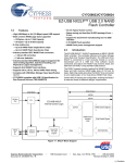
1
3.125 Gbps 4x4 LVDS Crosspoint Switch
with Transmit Pre-emphasis
and Receive Equalization
DS25CP104 Evaluation Kit
USER MANUAL
Part Number: DS25CP104EVK
For the latest documents concerning these products and evaluation kit, visit lvds.national.com.
Schematics and gerber files are also available at lvds.national.com.
February 2008
Rev. 0.2
DS25CP104EVK User Manual
Table of Contents
Table of Contents…..........................................................................................................2
Overview………………………………………………………………………………...3
DS25CP104 EVK Description …………………………………………………………4
CP104 Evaluation ………………………………………………………………………6
SMBus Evaluation ……………………………………………………………………..12
Typical Performance …………………………………………………………………...16
Page 2 of 17
DS25CP104EVK User Manual
Overview
The DS25CP104EVK is an evaluation kit designed for demonstrating performance of
DS25CP104, a 3.125 Gbps 4x4 LVDS Crosspoint Switch with Transmit Pre-emphasis
and Receive Equalization. The evaluation kit is comprised of the DS25CP104 with its
associated input and output SMA connectors and jumpers to manually select the desired
pre-emphasis or equalization, a USB to SMBus conversion circuit to control the SMBus
with a PC, and three FR4 striplines (15” (38.1cm), 30” (76.2cm), and 60” (152.4cm) ) to
exercise the devices’ signal conditioning features (pre-emphasis and equalization).
The purpose of this document is to familiarize the user with the DS25CP104EVK, to
suggest test setup procedures and instrumentation to test the device optimally, and to
guide the user through some typical measurements that demonstrate the performance of
the DS25CP104 in typical applications.
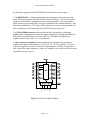
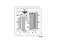
Figure 1. Photo of the DS25CP104EVK
Page 3 of 17
DS25CP104EVK User Manual
DS25CP104EVK Description
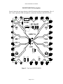
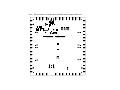
Figure 2 shows the top layer drawing of the PCB with the silkscreen annotations. The 4.5
by 4.5 inch, eight-layer PCB is designed to evaluate the functions of the DS25CP104.
Figure 2. Top Layer DS25CP104EVK
Page 4 of 17
DS25CP104EVK User Manual
For descriptive purposes the DS25CP104EVK can be broken into three parts:
1. The DS25CP104 IC with associated connectors and jumpers is the main part of the
board. The block diagram of the DS25CP104 is shown in Figure 3. The receive buffers
can be set to Off and Low equalization by the external pins EQ0 – EQ3; the transmit
buffers can be set to Off and Med. levels of pre-emphasis by the external pins PE0 – PE3.
Since data capabilities are 3.125 Gbps, SMA connectors are used to ensure minimal loss.
More information can be found about the DS25CP104 on the data sheets.
2. A USB to SMBus converter has been added to the evaluation kit to implement
SMBus switch configuration to control the signal conditioning. Through the SMBus the
DS25CP104 currently features four levels (Off, Low, Medium, and High) of preemphasis and two levels (Off, Low) of equalization.
ADDRn
SCL
SDA
EN_smb
3. Three channels of stripline have been added to the evaluation kit to test the preemphasis and equalization functions (15” (38.1cm), 30” (76.2cm), and 60” (152.4cm) ).
In practical applications, devices often drive long backplanes or cables. To help reduce
jitter caused from long backplanes or cables, pre-emphasis can be used for the drivers and
equalization for the receivers.
Figure 3. DS25CP104 Block Diagram
Page 5 of 17
DS25CP104EVK User Manual
DS25CP104 Evaluation
The DS25CP104 is a 3.125 Gbps LVDS Crosspoint Switch with four levels of transmit
pre-emphasis and two levels of receive equalization configured in the SMBus Mode and
two levels of transmit pre-emphasis and two levels of receive equalization configured via
external jumpers on the evaluation board in the Pin Mode.
Initial Pin Settings for Pin Mode Testing
Pin
SMBus Enable
EQ0 – EQ 3
Setting
L
L
PE0 – PE3
L
PWDN
H
Note
Disable SMbus
Equalization off,
See table
Pre-Emphasis off,
See table
Power Down off
S00
0
1
0
1
Input Selected
IN0
IN1
IN2
IN3
Switch Configuration Truth Tables
S01
0
0
1
1
Table 1. Input Select Pins Configuration for the Output OUT0
S11
0
0
1
1
S10
0
1
0
1
Input Selected
IN0
IN1
IN2
IN3
Table 2. Input Select Pins Configuration for the Output OUT1
Page 6 of 17
DS25CP104EVK User Manual
S21
0
0
1
1
S20
0
1
0
1
Input Selected
IN0
IN1
IN2
IN3
Table 3. Input Select Pins Configuration for the Output OUT2
S31
0
0
1
1
S30
0
1
0
1
Input Selected
IN0
IN1
IN2
IN3
Table 4. Input Select Pins Configuration for the Output OUT3
Signal Conditioning Tables
Output OUTn, n={0,1,2,3}
Pre-Emphasis Control Pin (PEn) State
Pre-Emphasis Level
0
Off
1
Medium
Table 5. Transmit Pre-emphasis Truth Table
Input INn, n={0,1,2,3}
Equalization Control Pin (EQn) State
Equalization Level
0
Off
1
Low
Table 6. Receive Equalization Truth Table
Stripline Length Table (also known as Test Channels)
Stripline
L1
L2
L3
Length
15” (38.1cm)
30” (76.2cm)
60” (152.4cm)
Table 7. Stripline length table
Page 7 of 17
Loss (dB) @ 1250 MHz
-3.6
-8.2
-14.5
DS25CP104EVK User Manual
Jitter Performance Testing with No Signal Conditioning
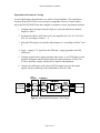
1. Configure the test setup as shown in Figure 4.
2. Set the desired INn to OUTn drivers by selecting S00, S01, S10, S11, S20, S21,
S30, S31 according to Tables 1 – 4.
3. Select the PEn and EQn jumpers to 0, according to tables 5 and 6.
4. Apply + supply (3.3V typical) to the VDD and – supply (ground) to the VSS
connectors.
5. Connect a signal source (signal generator, data source, or an LVDS driver) to the
desired INn inputs on the board and adjust the signal parameters (VOH, VOL,
VCM) so that they comply with the device input recommendations.
6. Connect an oscilloscope to the selected OUTn outputs and view the output signals
with an oscilloscope with the bandwidth of at least 5 GHz.
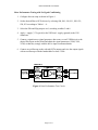
Figure 4. Jitter Performance Test Circuit
Page 8 of 17
DS25CP104EVK User Manual
Pre-Emphasis Performance Testing
In applications where data transmits over cables or long backplanes, the pre-emphasis
feature on the DS25CP104 transmitter helps to overcome media loss and reduce bit
errors; hence the DS25CP104EVK has three lengths of stripline to test the pre-emphasis
function.
1. Configure the test setup as shown in figure 5; select the desired test channel
lengths in Table 7.
2. Set the desired INn to OUTn drivers by selecting S00, S01, S10, S11, S20, S21
according to Tables 1 – 4.
3. Select the PEn jumpers to 1 and the EQn jumpers to 0, according to Tables 5 and
6.
4. Apply + supply (3.3V typical) to the VDD and – supply (ground) to the VSS
connectors.
5. Connect a signal source (signal generator, data source, or an LVDS driver) to the
desired INn inputs on the board and adjust the signal parameters (VOH, VOL,
VCM) so that they comply with the device input recommendations.
6. Connect an oscilloscope to the selected OUTn outputs and view the output signals
with an oscilloscope with a bandwidth of at least 5 GHz.
Figure 5. Pre-Emphasis Performance Test Circuit
Page 9 of 17
DS25CP104EVK User Manual
Equalization Performance Testing
In some applications, data transmits over cables or long backplanes. The equalization
function on the DS25CP104 receivers helps to compensate for loss of certain media;
hence the DS25CP104EVK has three lengths of stripline to test the equalization function.
1. Configure the test setup as shown in Figure 6; select the desired test channel,
lengths in Table 7.
2. Set the desired INn to OUTn drivers by selecting S00, S01, S10, S11, S20, S21,
S30, S31 according to Tables 1 – 4.
3. Select the PEn jumpers to 0 and the EQn jumpers to 1, according to Tables 5 and
6.
4. Apply + supply (3.3V typical) to the VDD and – supply (ground) to the VSS
connectors.
5. Connect a signal source (signal generator, data source, or an LVDS driver) to the
desired INn inputs on the board and adjust the signal parameters (VOH, VOL,
VCM) so that they comply with the device input recommendations.
6. Connect an oscilloscope to the selected OUTn outputs and view the output
signals with an oscilloscope with a bandwidth of at least 5 GHz.
Figure 6. Equalization Performance Test Circuit
Page 10 of 17
DS25CP104EVK User Manual
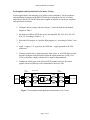
Pre-Emphasis and Equalization Performance Testing
In some applications, data transmits over cables or long backplanes. The pre-emphasis
and equalization functions on the DS25CP104 help to compensate for loss of certain
media; hence the DS25CP104EVK has three lengths of stripline to test the pre-emphasis
and equalization functions.
1. Configure the test setup as shown in Figure 7; select the desired test channel,
lengths in Table 7.
2. Set the desired INn to OUTn drivers by selecting S00, S01, S10, S11, S20, S21,
S30, S31 according to Tables 1 – 4.
3. Select the PEn jumpers to 1 and the EQn jumpers to 1, according to Tables 5 and
6.
4. Apply + supply (3.3V typical) to the VDD and – supply (ground) to the VSS
connectors.
5. Connect a signal source (signal generator, data source, or an LVDS driver) to the
desired INn inputs on the board and adjust the signal parameters (VOH, VOL,
VCM) so that they comply with the device input recommendations.
6. Connect an oscilloscope to the selected OUTn outputs and view the output
signals with an oscilloscope with a bandwidth of at least 5 GHz.
TEST
CHANNEL
TEST
CHANNEL
DS25CP104EVK
50
Microstrip
¼ DS25CP104
50
Microstrip
L=4"
L=4"
L=4"
L=4"
50
Microstrip
50
Microstrip
PATTERN
GENERATOR
OSCILLOSCOPE
Figure 7. Pre-emphasis and Equalization Performance Test Circuit
Page 11 of 17
DS25CP104EVK User Manual
SMBus Evaluation
Introduction:
The CP104 can be evaluated in the Pin Mode using the external pins, or in the SMBus
mode. The following section describes how to load and run the Analog Launch Pad from
National Semiconductor, a proprietary interface, used to access the SMBus registers of
the CP104. The 1st time the application is run on a PC, and only the 1st time, the
application file needs to be downloaded, extracted, and then the appropriate driver needs
to be enabled. Any time after that, on the same PC, you need only to setup the
CP104EVK and then proceed to using the Analog Launch Pad.
Loading and running the application file
•
•
•
•
Download the application file from
http://www.national.com/appinfo/lvds/ds25cp104evk.html
Place in any folder on your PC, and run the file by double clicking on the file
from Windows Explorer (or My Computer); this will extract the file and place it
in C:\Program Files\National Semiconductor Corp folder.
The Analog Launch Pad will now function only in the Demo mode.
The Analog Launch Pad is designed to function on Windows 98/2000/xp
Setup the CP104EVK
(When using the USB, power should be off to the CP104 and USB unplugged when
changing cables or changing the jumper pins.)
1. Install jumper pins as follows:
J21, SMBus Enable
J4
J3
J15, J16
J18, J19
J24, J22
J20, J23
H
inserted
removed
removed
L
H
L
Enables the SMBus
USB Controller Reset
EEPROM write protect
S00 (SCL), S01 (SDA)
Address
Address
Table 8. Jumpers on the CP104EVK for SMBus use
2. Configure the test setup as desired, examples are fig. 4 – fig. 7.
3. Supply 3.3 V Power to board.
Page 12 of 17
DS25CP104EVK User Manual
Load the driver
This needs to be done only once for a particular PC.
•
•
Plug in the USB cable from the PC to the CP104 EVK; a small window should
appear in the lower right corner of the PC recognizing new hardware. If the
bubble says “USB device not recognized”, or nothing happens, check the
jumper configuration, if still does not work remove jumper on J4 for 5 sec,
and then replace. The USB controller is now reset and should be in
communication with the PC; this can be known by “Hi speed USB device plugged
into non Hi Speed USB hub” appearing in the window.
Follow the instructions for New Hardware Wizard, which may take up to one
minute to run.
a. select “Install from a list or specific location”
b. select “Don’t search I will choose the driver to install”
c. select “Have disk”
d. Browse to “C:\Program Files\National Semiconductor Corp\Analog
LaunchPAD v1.07\Drivers”
e. select “NSC ALP Nano” from the list
f. install the driver
g. hit “Continue Anyway” if windows compatibility window is displayed
h. finish, you are now ready to run the Analog Launch Pad
Page 13 of 17
DS25CP104EVK User Manual
Page 14 of 17
DS25CP104EVK User Manual
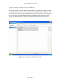
Using the Analog Launch Pad for the CP104EVK
The Analog Launch Pad from National Semiconductor is a proprietary interface created
to assist developers to test their designs and systems using National’s evaluation boards;
the CP104EVK interface has been designed into the Analog Launch Pad. The registers of
the CP104 can be accessed through this interface enabling all the functions accessed
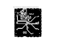
through the SMBus. Below is a picture of the Analog Launch Pad, CP104 interface:
Figure 8. Analog Launch Pad, CP104 interface
Page 15 of 17
DS25CP104EVK User Manual
To use the interface:
•
Run the application Analog Launch Pad and select CP104 Nano. For the Analog
Launch Pad to connect, the board must be powered with the appropriate jumper
selections and the USB driver must be functioning. Otherwise it will open into the
Demo mode.
•
Select the “Register” folder and enter the register that you want to change, make
the appropriate changes, and then hit Apply. Register descriptions can be found in
the DS25CP104 datasheets.
Use only Apply to make changes; Refresh, Refresh All, Display, Load, and
Save bubbles should not be used.
•
•
A selected square corresponds to a ‘1’ while a blank square corresponds to a ‘0’.
•
To change the levels of Pre Emphasis or Equalization, you must first go to
“Control” register and enable “Ignore External PE” and “Ignore External EQ”
before adjusting the signal conditioning through the SMBus.
•
To use the “Loss of Signal”, you must first go to “Control” register and enable
“LOS”.
• The Verbose Description square switches to a more descriptive text.
Page 16 of 17
DS25CP104EVK User Manual
• Typical Performance
When evaluating the CP104 EVK, the eye diagram response should be similar to those
below (measured on the Tektronix CSA 8000)
The DS25CP104 3.125 Gbps PRBS-7 output eye
diagram with no STRIPLINE connected and with
PE/EQ = Off
The DS25CP104 3.125 Gbps PRBS-7 output eye
diagram after the STRIPLINE 1 (15” FR4) and with
EQ = Low. See Figure 6 for the Setup used.
The DS25CP104 3.125 Gbps PRBS-7 output eye
diagram before the STRIPLINE2 (30” FR4) and
with PE/EQ = Off
The DS25CP104 3.125 Gbps PRBS-7 output eye
diagram before the STRIPLINE 2 (30” FR4) and
with PE = Med. See Figure 5 for the Setup used.
Page 17 of 17
Note: This document is considered uncontrolled unless stamped otherwise.
Note: This document is considered uncontrolled unless stamped otherwise.
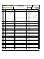
ENERCON -
BILL OF MATERIALS
TITLE:
Main Product:
NATIONAL SEMICONDUCTOR
PCBA, DS25CP104EVK, ROHS
Rev: Rev By: Rev Date:
PL Number:
Z3071-01 0
Responsible Eng/Mgr:
PCBA, DS25CP104 EVK
Item Part Type
1 PCB
Part Number/Value
Mfg
P-05885R0
NoSub
Description
Qty
DS25CP104EVK: 5.25x5.25x.060in, 8 layer
1
Released
Creator:
Creation Date:
Arlene Fox
3/28/2007
Ref Des
SMT
PL Status:
3/28/2007
Notes
Bd: (133.35x
133.35mm)
Panel: (
10.60x5.25in)
(269.24x
133.35mm) 2
bds/panel
Rev
0
2
3 IC
24LC128-I/SN
MICROCHIP
128K bit Serial EEPROM 2.5V, SOIC8, PbFree
1
X
U3
0
4 IC
CY7C68013A-56LFXC
CYPRESS
EZ-USB FX2 USB Microcontroller, QFN56,
Pb-Free
1
X
U1
0
5 IC
DS25CP104
NAT
6 IC
LP38691SD-3.3/NOPB
NAT
Linear Regulator, 3.3V, LLP6, Pb-Free
1
X
U2
0
7 IC
PGB1040805
LF
ESD Suppressor, 0805, Pb-Free
1
X
U4
0
ERJ-3GEY0R00
PANA
0 Ohm 1/10W ±5% 0603, Pb-Free
3
X
R4,5,14
0
<ALT>
CRCW06030000Z0EA
VISHAY
0 Ohm 1/10W ±5% 0603, Pb-Free
<ALT>
MCR03EZPJ000
ROHM
0 Ohm 1/10W ±5% 0603, Pb-Free
<ALT>
RC0603JR-070RL
YAGEO
0 Ohm 1/10W ±5% 0603, Pb-Free
5
X
R3,8-9,12,13
0
2
X
R1-2
0
2
X
R6,7
0
2
X
R10-11
0
1
U5
Customer
Supplied
0
8
9 RES
10 RES
ERJ-3GEYJ103
PANA
10K 1/10W ±5% 0603 200ppm, Pb-Free
<ALT>
CRCW060310K0JNEA
VISHAY
10K 1/10W ±5% 0603 200ppm, Pb-Free
<ALT>
RK73B1JTTD103J
KOA
10K 1/10W ±5% 0603 200ppm, Pb-Free
ERJ-3GEYJ220
PANA
22 Ohm 1/10W ±5% 0603 200ppm, Pb-Free
CRCW060322R0JNEA
VISHAY
22 Ohm 1/10W ±5% 0603 200ppm, Pb-Free
11 RES
<ALT>
<ALT>
12 RES
<ALT>
<ALT>
13 RES
RK73B1JTTD220J
KOA
22 Ohm 1/10W ±5% 0603 200ppm, Pb-Free
ERJ-3GEYJ222
PANA
2.2K 1/10W ±5% 0603 200ppm, Pb-Free
CRCW06032K20JNEA
VISHAY
2.2K 1/10W ±5% 0603 200ppm, Pb-Free
RK73B1JTTD222J
KOA
2.2K 1/10W ±5% 0603 200ppm, Pb-Free
ERJ-8GEY0R00
PANA
0 Ohm 1/4W ±5% 1206, Pb-Free
1:12:35 PM, 4/20/2007
Confidential and Proprietary. This document is considered uncontrolled unless stamped otherwise.
Page
1 of 3
ENERCON -
BILL OF MATERIALS
TITLE:
Main Product:
NATIONAL SEMICONDUCTOR
PCBA, DS25CP104EVK, ROHS
Rev: Rev By: Rev Date:
PL Number:
Z3071-01 0
Responsible Eng/Mgr:
PCBA, DS25CP104 EVK
Item Part Type
<ALT>
Part Number/Value
Mfg
NoSub
Description
CRCW12060000Z0EA
VISHAY
0 Ohm 1/4W ±5% 1206, Pb-Free
0402YC103KAT
AVX
.01µF, 16V, ±10%, 0402, Ceramic, X7R,
Pb-Free
<ALT>
C0402C103K4RAC
KEMET
.01µF, 16V, ±10%, 0402, Ceramic, X7R,
Pb-Free
<ALT>
ECJ-0EB1C103K
PANA
.01µF, 16V, ±10%, 0402, Ceramic, X7R,
Pb-Free
08055A180JAT
AVX
18pF, 50V, ±5%, 0805, Ceramic, NP0, PbFree
<ALT>
C0805C180J5GAC
KEMET
18pF, 50V, ±5%, 0805, Ceramic, NP0, PbFree
<ALT>
ECJ-2VC1H180J
PANA
18pF, 50V, ±5%, 0805, Ceramic, NP0, PbFree
17 CAP
C0402C104K8RAC
KEMET
.1µF, 10V, ±10%, 0402, Ceramic, X7R, PbFree
18 CAP
C1206C225K4RAC
KEMET
2.2µF, 16V, ±10%, 1206, Ceramic, X7R,
Pb-Free
ECJ-3YB1C225K
PANA
2.2µF, 16V, ±10%, 1206, Ceramic, X7R,
Pb-Free
MMZ1608R301A
TDK
HCM49-24.000MABJ
Qty
Released
Creator:
Creation Date:
Arlene Fox
3/28/2007
Ref Des
SMT
PL Status:
3/28/2007
Notes
Rev
14
15 CAP
2
X
C15,17
0
2
X
C11-12
0
10
X
C1,4-8,10,1314,16
0
4
X
C2,3,9,18
0
Ferrite, 300 Ohm, .5A, 0603, Pb Free
2
X
FB1-2
0
CITIZEN
Crystal, 24.0000MHz, SMD, 18pF, Pb-Free
1
X
Y1
0
1206L050
LF
.5A, Resettable, SMT, .09 Ohms, Pb Free
1
X
F1
0
26 CONN
1287-ST
KEYSTONE
Faston, Male, .250x.032, Pb-Free
2
J25-26
0
27 CONN
142-0701-851
EMERSON
SMA, Jack Receptacle, 50 OHM, Pb-Free
SMA1-28
0
28 CONN
61729-0010
FCI
USB-B, 4p, R/A, Pb-Free
1
J1
0
29 CONN
TSW-102-07-G-S
SAMTEC
Header, 2p, Male, .100"sp, Gold, Pb-Free
2
J3-4
0
30 CONN
TSW-103-07-G-S
SAMTEC
Header, 3p, Male, .100"sp, Gold, Pb-Free
18
J7-24
0
16 CAP
<ALT>
19
20 FILTER
21
22 XTAL
23
24 FUSE
25
1:12:35 PM, 4/20/2007
28
Confidential and Proprietary. This document is considered uncontrolled unless stamped otherwise.
Page
2 of 3
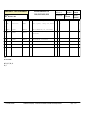
ENERCON -
BILL OF MATERIALS
TITLE:
Main Product:
NATIONAL SEMICONDUCTOR
PCBA, DS25CP104EVK, ROHS
Rev: Rev By: Rev Date:
PL Number:
Z3071-01 0
Responsible Eng/Mgr:
PCBA, DS25CP104 EVK
Item Part Type
31 CONN
Part Number/Value
Mfg
NoSub
Description
Qty
Released
Creator:
Creation Date:
Arlene Fox
3/28/2007
Ref Des
SMT
PL Status:
3/28/2007
Notes
J2
Rev
TSW-105-07-G-S
SAMTEC
Header, 5p, Male, .100"sp, Gold, Pb-Free
1
0
T-05889R0
ENERCON
STENCIL FABRICATION, TOP, DS25CP104EVK
1
0
T-05890R0
ENERCON
STENCIL FABRICATION, BOTTOM,
DS25CP104EVK
1
0
36 REF
C-05886R0
ENERCON
FABRICATION DWG, DS25CP104EVK
0
37 REF
C-05888R0
ENERCON
PALLET DWG, DS25CP104EVK
0
38 REF
S-05887R0
ENERCON
SCHEMATIC, DS25CP104EVK
0
32
33 STENCL
34 STENCL
35
39
40
41
Notes:
DO NOT STUFF:
R15,16,17,18,19
J5,6
1:12:35 PM, 4/20/2007
Confidential and Proprietary. This document is considered uncontrolled unless stamped otherwise.
Page
3 of 3
Note: This document is considered uncontrolled unless stamped otherwise.
Note: This document is considered uncontrolled unless stamped otherwise.
Note: This document is considered uncontrolled unless stamped otherwise.
Note: This document is considered uncontrolled unless stamped otherwise.
Note: This document is considered uncontrolled unless stamped otherwise.
Note: This document is considered uncontrolled unless stamped otherwise.
Note: This document is considered uncontrolled unless stamped otherwise.
Note: This document is considered uncontrolled unless stamped otherwise.
Note: This document is considered uncontrolled unless stamped otherwise.
Note: This document is considered uncontrolled unless stamped otherwise.
Note: This document is considered uncontrolled unless stamped otherwise.
Note: This document is considered uncontrolled unless stamped otherwise.
Note: This document is considered uncontrolled unless stamped otherwise.
Note: This document is considered uncontrolled unless stamped otherwise.
IMPORTANT NOTICE
Texas Instruments Incorporated and its subsidiaries (TI) reserve the right to make corrections, modifications, enhancements, improvements,
and other changes to its products and services at any time and to discontinue any product or service without notice. Customers should
obtain the latest relevant information before placing orders and should verify that such information is current and complete. All products are
sold subject to TI’s terms and conditions of sale supplied at the time of order acknowledgment.
TI warrants performance of its hardware products to the specifications applicable at the time of sale in accordance with TI’s standard
warranty. Testing and other quality control techniques are used to the extent TI deems necessary to support this warranty. Except where
mandated by government requirements, testing of all parameters of each product is not necessarily performed.
TI assumes no liability for applications assistance or customer product design. Customers are responsible for their products and
applications using TI components. To minimize the risks associated with customer products and applications, customers should provide
adequate design and operating safeguards.
TI does not warrant or represent that any license, either express or implied, is granted under any TI patent right, copyright, mask work right,
or other TI intellectual property right relating to any combination, machine, or process in which TI products or services are used. Information
published by TI regarding third-party products or services does not constitute a license from TI to use such products or services or a
warranty or endorsement thereof. Use of such information may require a license from a third party under the patents or other intellectual
property of the third party, or a license from TI under the patents or other intellectual property of TI.
Reproduction of TI information in TI data books or data sheets is permissible only if reproduction is without alteration and is accompanied
by all associated warranties, conditions, limitations, and notices. Reproduction of this information with alteration is an unfair and deceptive
business practice. TI is not responsible or liable for such altered documentation. Information of third parties may be subject to additional
restrictions.
Resale of TI products or services with statements different from or beyond the parameters stated by TI for that product or service voids all
express and any implied warranties for the associated TI product or service and is an unfair and deceptive business practice. TI is not
responsible or liable for any such statements.
TI products are not authorized for use in safety-critical applications (such as life support) where a failure of the TI product would reasonably
be expected to cause severe personal injury or death, unless officers of the parties have executed an agreement specifically governing
such use. Buyers represent that they have all necessary expertise in the safety and regulatory ramifications of their applications, and
acknowledge and agree that they are solely responsible for all legal, regulatory and safety-related requirements concerning their products
and any use of TI products in such safety-critical applications, notwithstanding any applications-related information or support that may be
provided by TI. Further, Buyers must fully indemnify TI and its representatives against any damages arising out of the use of TI products in
such safety-critical applications.
TI products are neither designed nor intended for use in military/aerospace applications or environments unless the TI products are
specifically designated by TI as military-grade or "enhanced plastic." Only products designated by TI as military-grade meet military
specifications. Buyers acknowledge and agree that any such use of TI products which TI has not designated as military-grade is solely at
the Buyer's risk, and that they are solely responsible for compliance with all legal and regulatory requirements in connection with such use.
TI products are neither designed nor intended for use in automotive applications or environments unless the specific TI products are
designated by TI as compliant with ISO/TS 16949 requirements. Buyers acknowledge and agree that, if they use any non-designated
products in automotive applications, TI will not be responsible for any failure to meet such requirements.
Following are URLs where you can obtain information on other Texas Instruments products and application solutions:
Products
Applications
Audio
www.ti.com/audio
Automotive and Transportation www.ti.com/automotive
Amplifiers
amplifier.ti.com
Communications and Telecom www.ti.com/communications
Data Converters
dataconverter.ti.com
Computers and Peripherals
www.ti.com/computers
DLP® Products
www.dlp.com
Consumer Electronics
www.ti.com/consumer-apps
DSP
dsp.ti.com
Energy and Lighting
www.ti.com/energy
Clocks and Timers
www.ti.com/clocks
Industrial
www.ti.com/industrial
Interface
interface.ti.com
Medical
www.ti.com/medical
Logic
logic.ti.com
Security
www.ti.com/security
Power Mgmt
power.ti.com
Space, Avionics and Defense
www.ti.com/space-avionics-defense
Microcontrollers
microcontroller.ti.com
Video and Imaging
www.ti.com/video
RFID
www.ti-rfid.com
OMAP Mobile Processors
www.ti.com/omap
Wireless Connectivity
www.ti.com/wirelessconnectivity
TI E2E Community Home Page
e2e.ti.com
Mailing Address: Texas Instruments, Post Office Box 655303, Dallas, Texas 75265
Copyright © 2012, Texas Instruments Incorporated